Amimon AMN12310 AMN12310 Receiver – WHDI Wireless Modules User Manual Copy of AMN12310 Data sheet 02 09 08
Amimon Ltd. AMN12310 Receiver – WHDI Wireless Modules Copy of AMN12310 Data sheet 02 09 08
UserManual.wiki
>
Amimon
>
AMN12310 User Manual
Users Manual
Navigation menu
Upload a User Manual
Namespaces
Wiki Guide
HTML
PDF
Info
Views
User Manual
Discussion / Help
Navigation
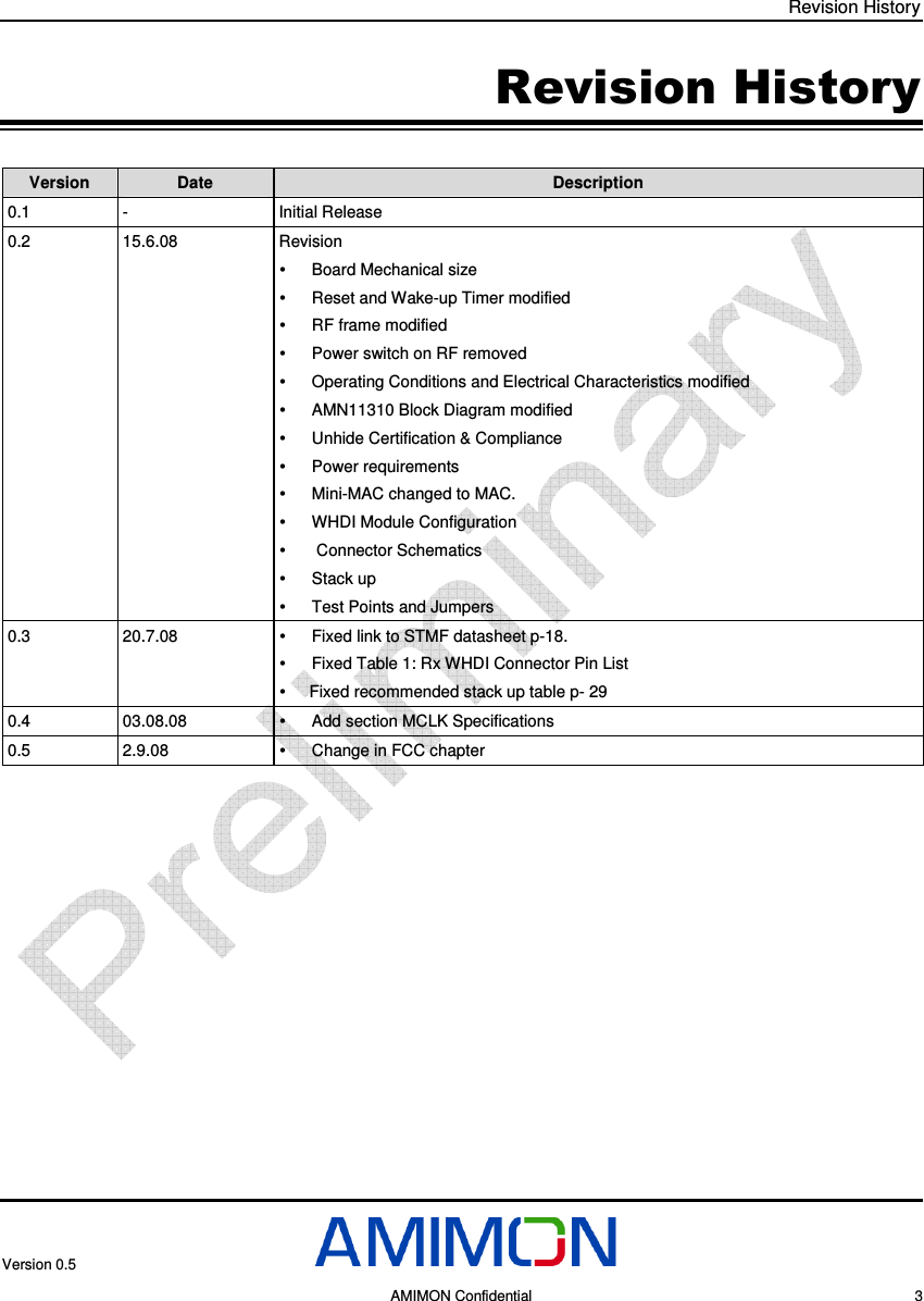

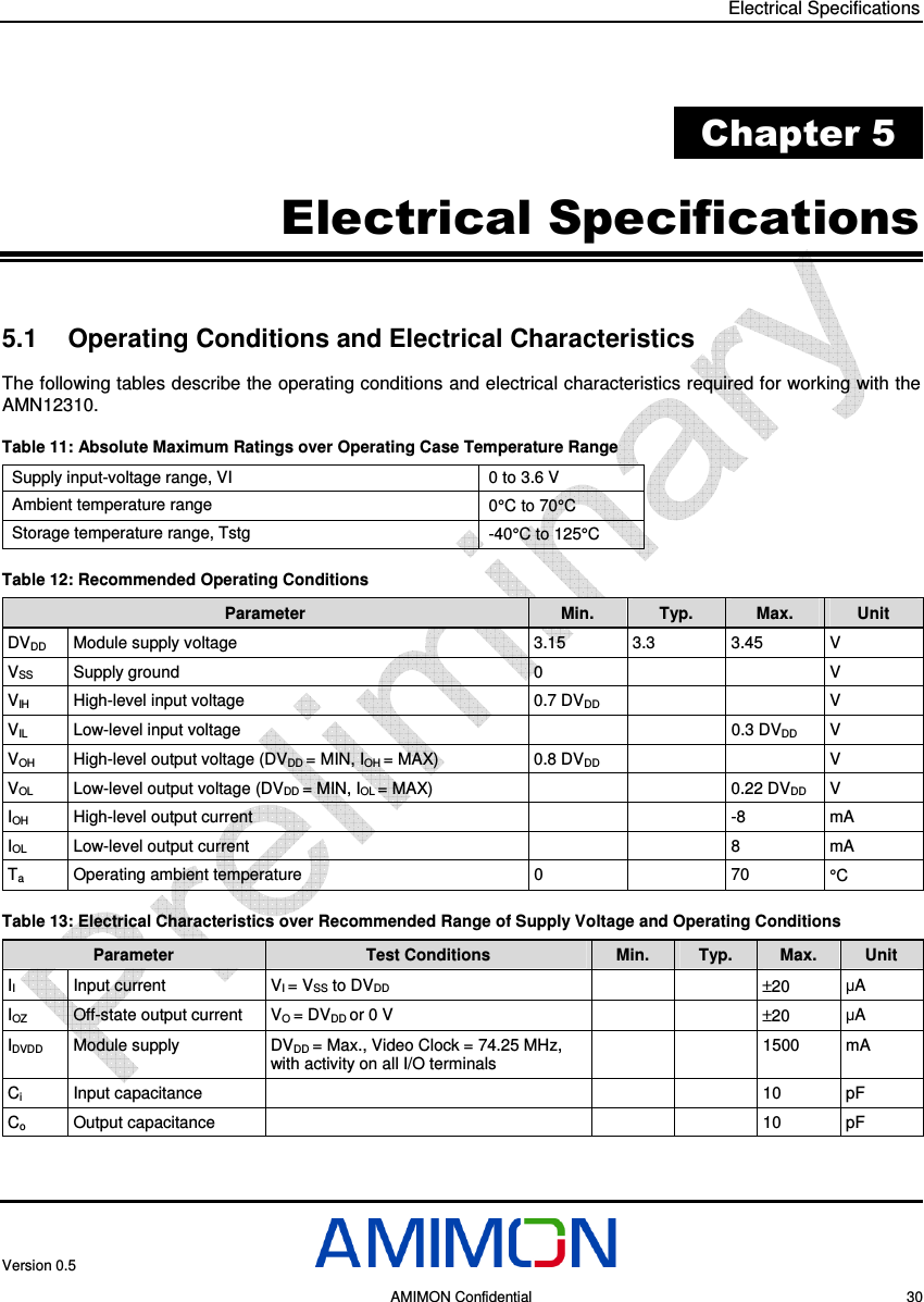
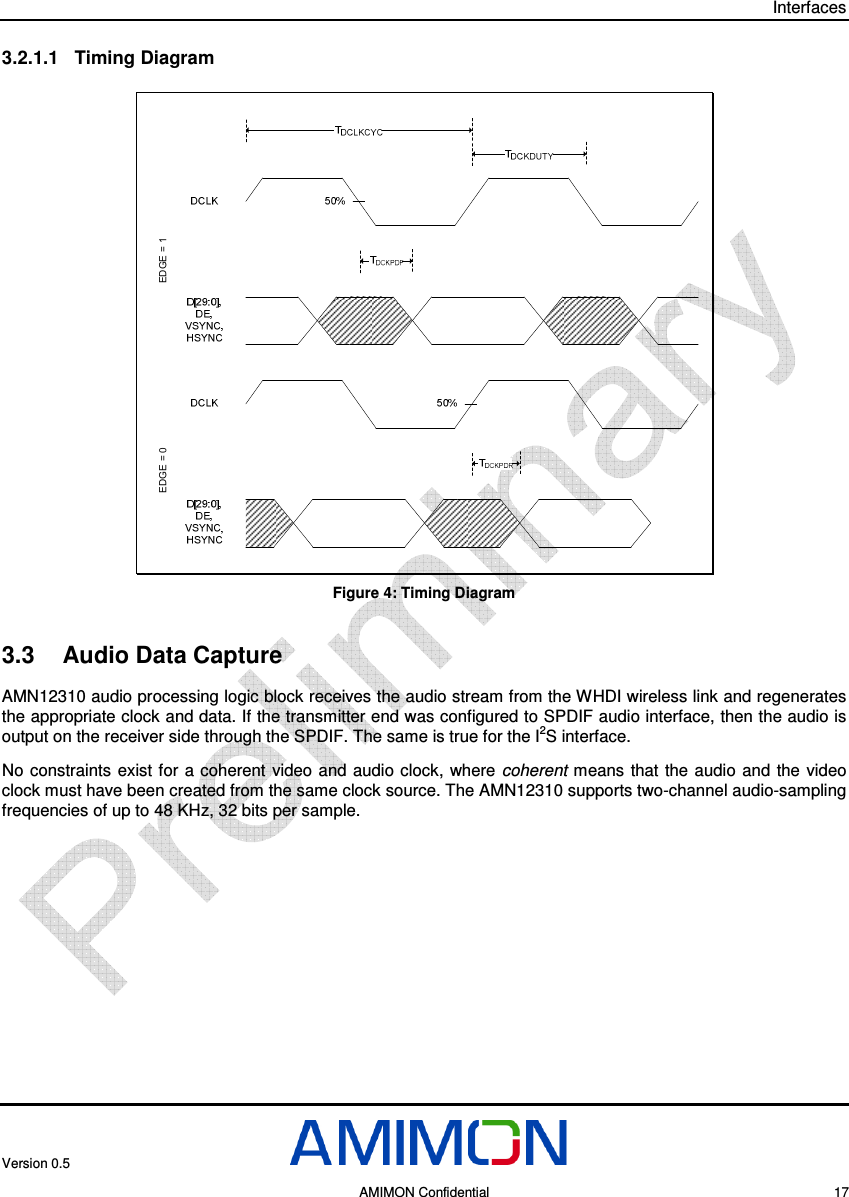
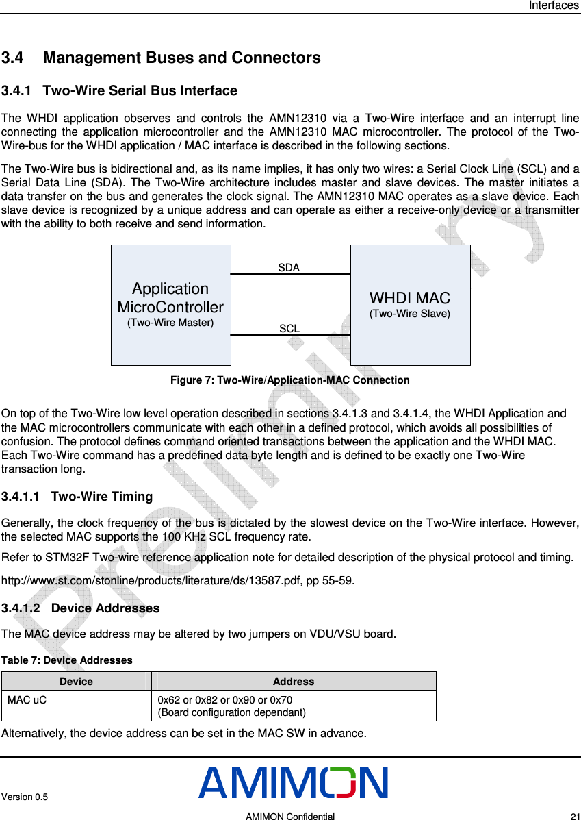
![Interfaces Version 0.5 AMIMON Confidential 16 Common Video Output Format Table 2 lists the common supported video output resolutions. Table 2: Common Supported Video Input Resolutions Input Pixel Clock (MHz) Color Space Video Format Bus Width 480i 480p XGA 720p 1080i RGB/YCbCr 4:4:4 24 27 27 65 74.25 74.25 Video Channel Mapping The 30 bit video output signals are mapped to the RGB and YCbCr color space according to the options described in the following table: Table 3: Video Channel Mapping Option D[29:20] D[19:10] D[9:0] #1 RED (Cr) GREEN (Y) BLUE (Cb) #2 RED (Cr) BLUE (Cb) GREEN (Y) #3 GREEN (Y) RED (Cr) BLUE (Cb) #4 GREEN (Y) BLUE (Cb) RED (Cr) #5 BLUE (Cb) RED (Cr) GREEN (Y) #6 BLUE (Cb) GREEN (Y) RED (Cr) The AMN123100 allows any of the output video channels options. The first option is the default from power-up. In order to change the video channel mapping, refer to the appropriate programmer's reference guide. 3.2 Video Interface Output Timing Diagram 3.2.1 Timing Requirements Important: The following parameters relate to the AMN2210 baseband chipset and not to the entire AMN12310 board. Table 4: Video Interface Symbol Parameter MIN TYP MAX Units TDCKCYC DCLK period 12.5 40 Ns TDCKFREQ DCLK frequency 25* 80 MHz TDCKDUTY DCLK duty cycle 40% 60% Ns TDCKPDR Propagation delay after DCLK rising edge 1.0 4.0 Ns TDCKPDF Propagation delay after DCLK falling edge 1.0 4.0 Ns * It is possible to support lower clock frequency using an external PLL for video clock generation.](https://usermanual.wiki/Amimon/AMN12310/User-Guide-997437-Page-16.png)
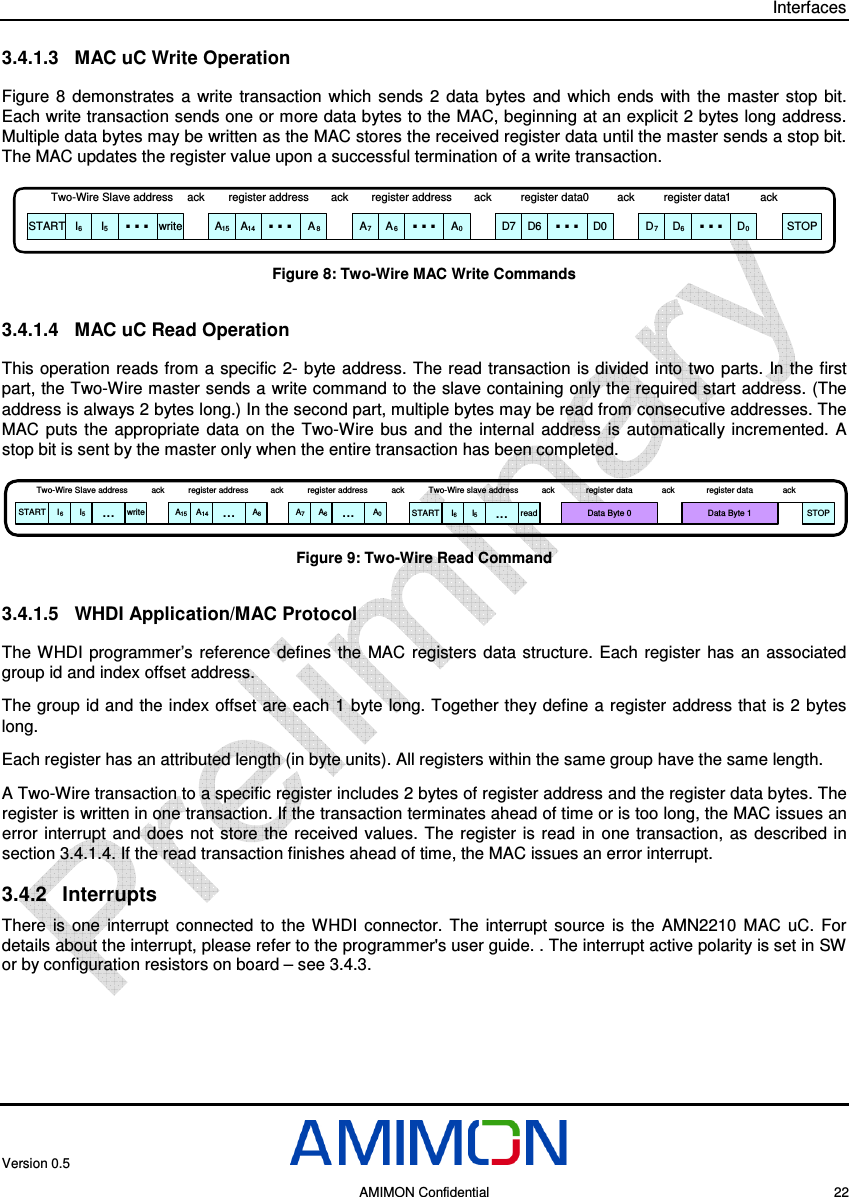
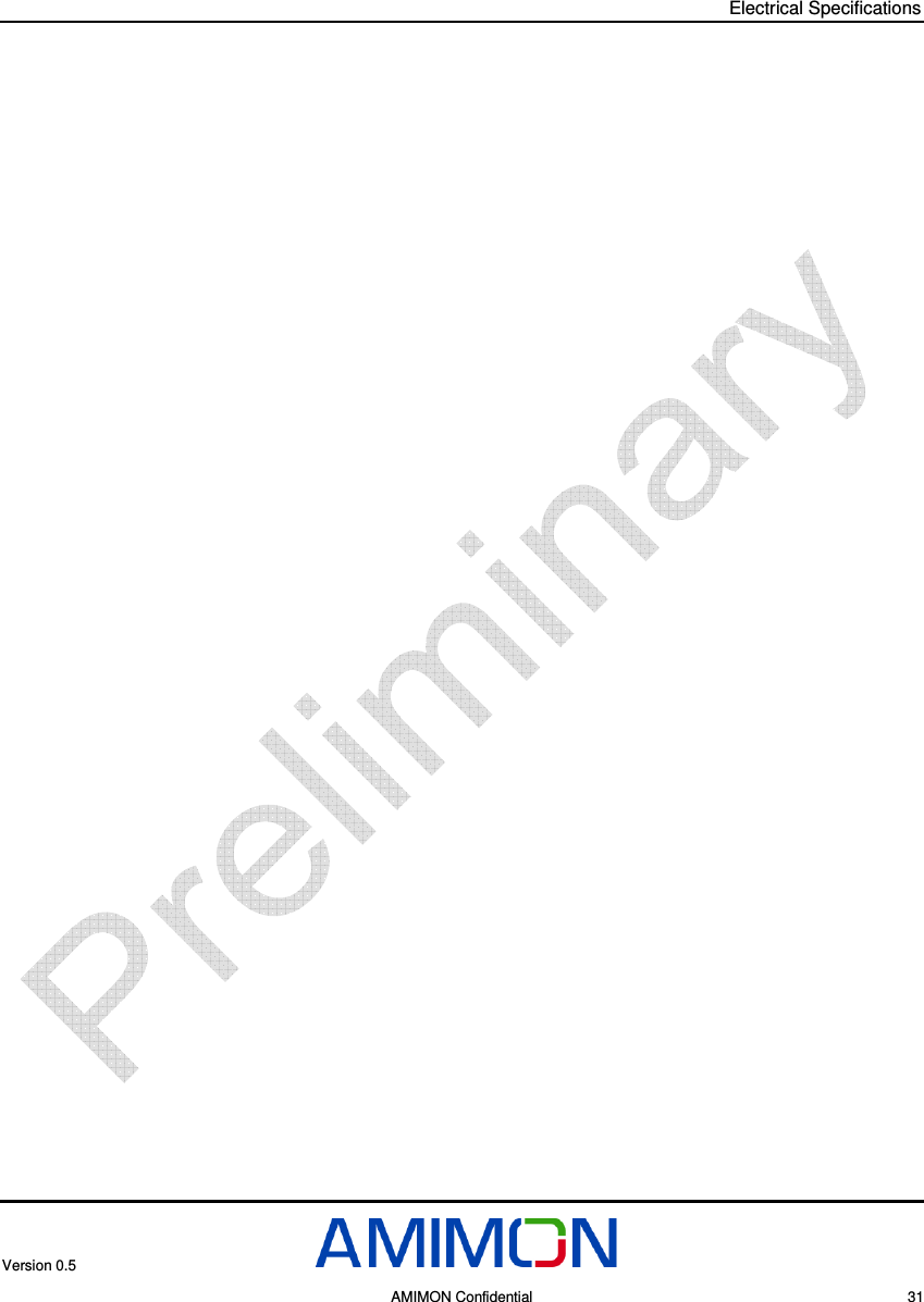
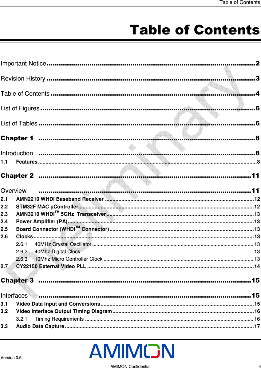
![Interfaces Version 0.5 AMIMON Confidential 23 3.4.3 WHDI Module Configuration In order to distinguish between boards and by the SW, there is an on board ID that can be read by the STM32F. WHDI_MODULE_ID (Details) Tx="0", Rx="1" Interrupt Polarity: "0"=falling, "1"=rising I2C Address: "00"=0x62, "01"=0x72, 10"=0x60, 11"=0x70 MODULE_ID Comments Amimon Project Part Number [7] [6] [5] [4] [3] [2] [1] [0] AMN11310 Rev. 2.0 1 0 0 0 0 0 0 0 AMN12310 Rev. 2.0 1 0 1 0 0 0 1 0 3.5 Reset and Wake-up Timer The AMN11100 has one hard RESET input pin connected directly to the AMN2110 and to the STM32F uC, as described in Figure 11. Assertion of the STM32F reset switches the clock of uC to the internal oscillator until the Albatross does not assert an INIT_DONE interrupt. Assertion of the Albatross reset enables the generation of the 10 MHz clock. After a hard reset, the MAC asserts the SW reset signal which just clears the registers without resetting the clock generation scheme. When the INIT_DONE is asserted, it indicates the completion of the Albatross initialization and that the 10 MHz clock is stable. At that point, the uC switches to the external clock source from the Albatross and enable communication with the application microcontroller. clkrstT−STrstTinitT Figure 10: Reset Time Diagram](https://usermanual.wiki/Amimon/AMN12310/User-Guide-997437-Page-23.png)
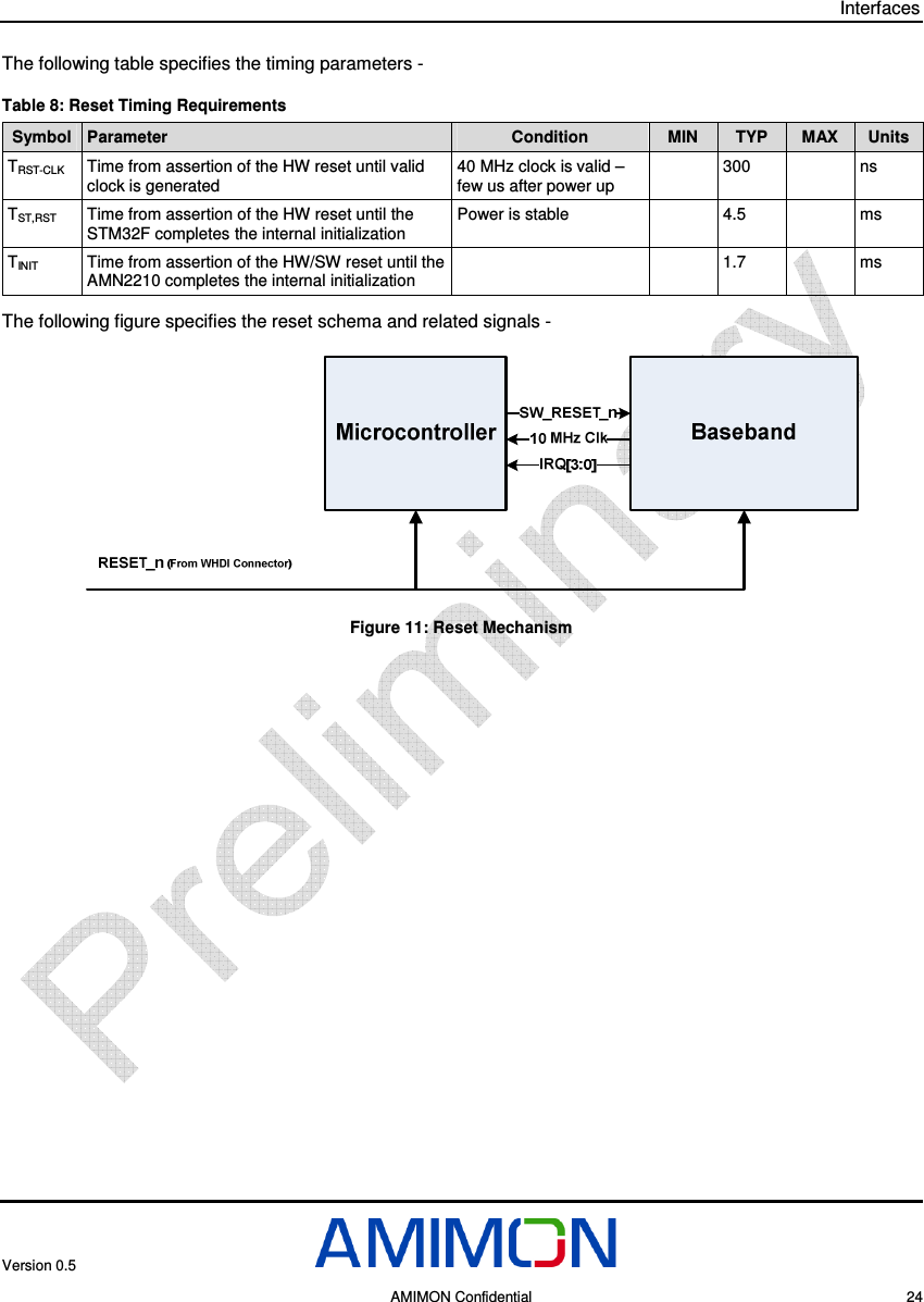

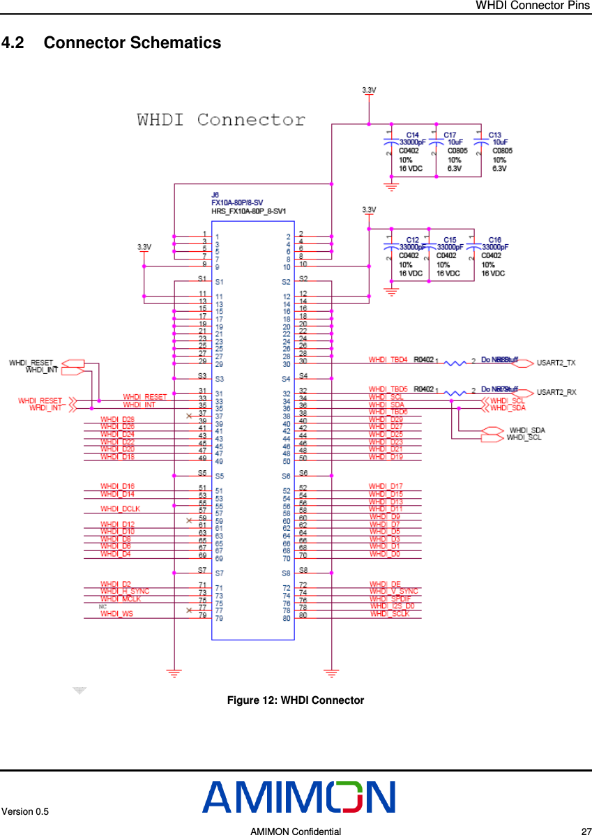
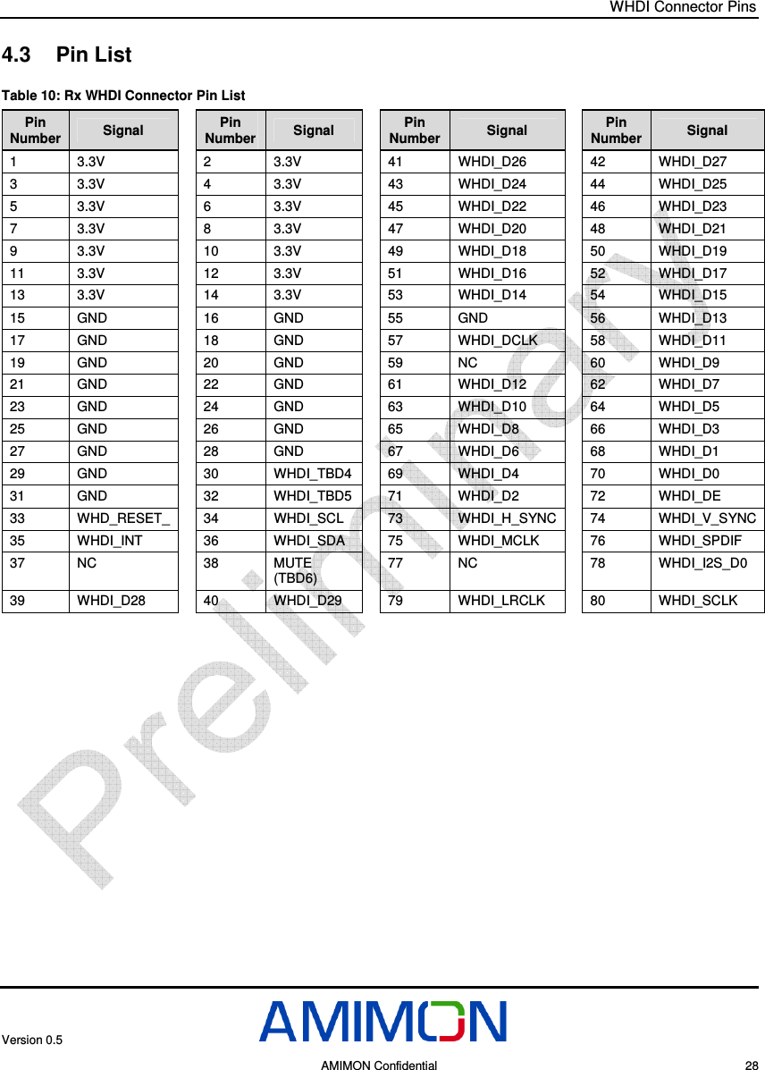
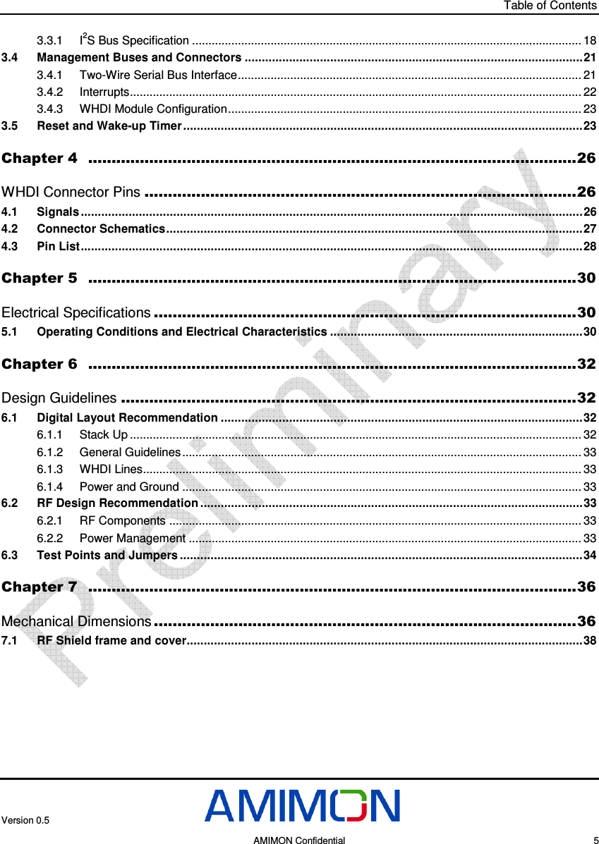
![WHDI Connector Pins Version 0.5 AMIMON Confidential 26 Chapter 4 WHDI Connector Pins 4.1 Signals Table 9: WHDI Connector Signals # of Pins Pin Name Description/Functionality Group Direction Remarks 30 D[29:0] 30-bit RGB (10:10:10) or YCrCb (10:10:10) Video Out 1 DCLK Video data clock Video Out Up to 78.125 MHz 1 DE Data enable Video Out 1 H_SYNC Horizontal sync Video Out 1 V_SYNC Vertical sync Video Out 1 SPDIF SPDIF audio interface Audio Out 1 SD I2S audio interface Serial Data signals Audio Out 1 SCLK I2S continuous serial clock Audio Out Up to 3.072Mbps 1 WS(LRCLK) I2S Word Select (Left/right clock) which defines also the sampling rate Audio Out 1 MCLK I2S master clock coherent to WS according to specified ratio Audio Out Rate is adjustable on RX side 1 SDA Two-wire Serial Bus Data (Slave Mode) Control I/O Control I/F for WHDI 1 SCL Two-wire Serial Bus Clock (Slave Mode) Control In Control I/F for WHDI 1 INT Interrupt from WHDI module Control Out 1 RESET Reset / Power-down line Control In 1 MUTE (TBD6) MUTE signal Audio Out Signals audio error and can be used by the next audio device down the line to mute the audio when errors occur 2 TBD[5:4] TBD4, TBD5, are reserved in, AMN12310 as an option for RS232 connection to STM32F UART2. TBD TBD 8 3.3V VCC Power Power 300 mA maximum rating per pin 17 GND Ground Power Power](https://usermanual.wiki/Amimon/AMN12310/User-Guide-997437-Page-26.png)