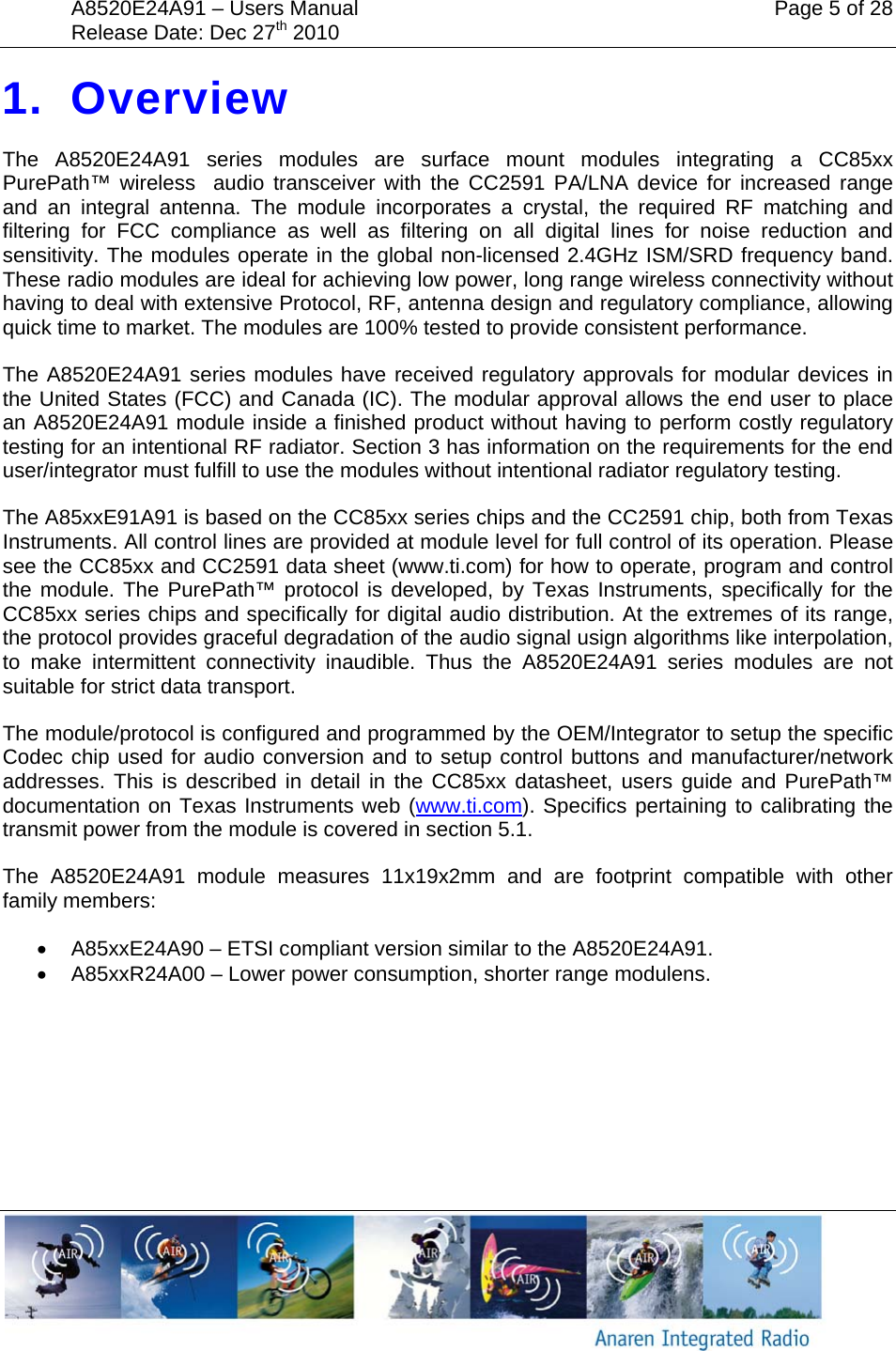
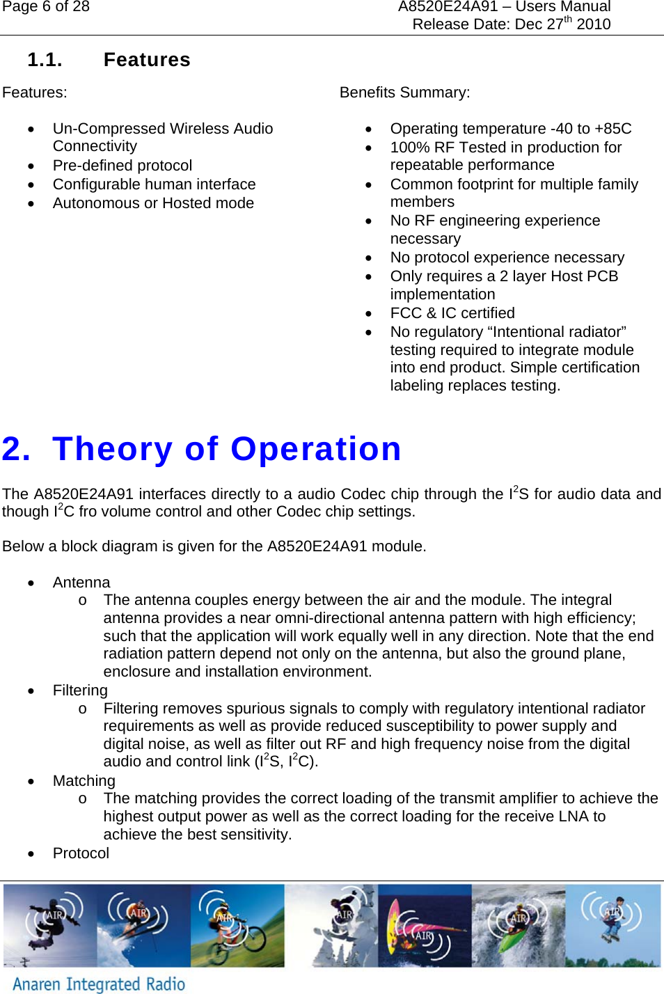
Anaren A10051701 2.4GHz Transceiver User Manual
Anaren, Inc. 2.4GHz Transceiver Users Manual
UserManual.wiki
>
Anaren
>
A10051701 User Manual
Users Manual
Navigation menu
Upload a User Manual
Namespaces
Wiki Guide
HTML
PDF
Info
Views
User Manual
Discussion / Help
Navigation


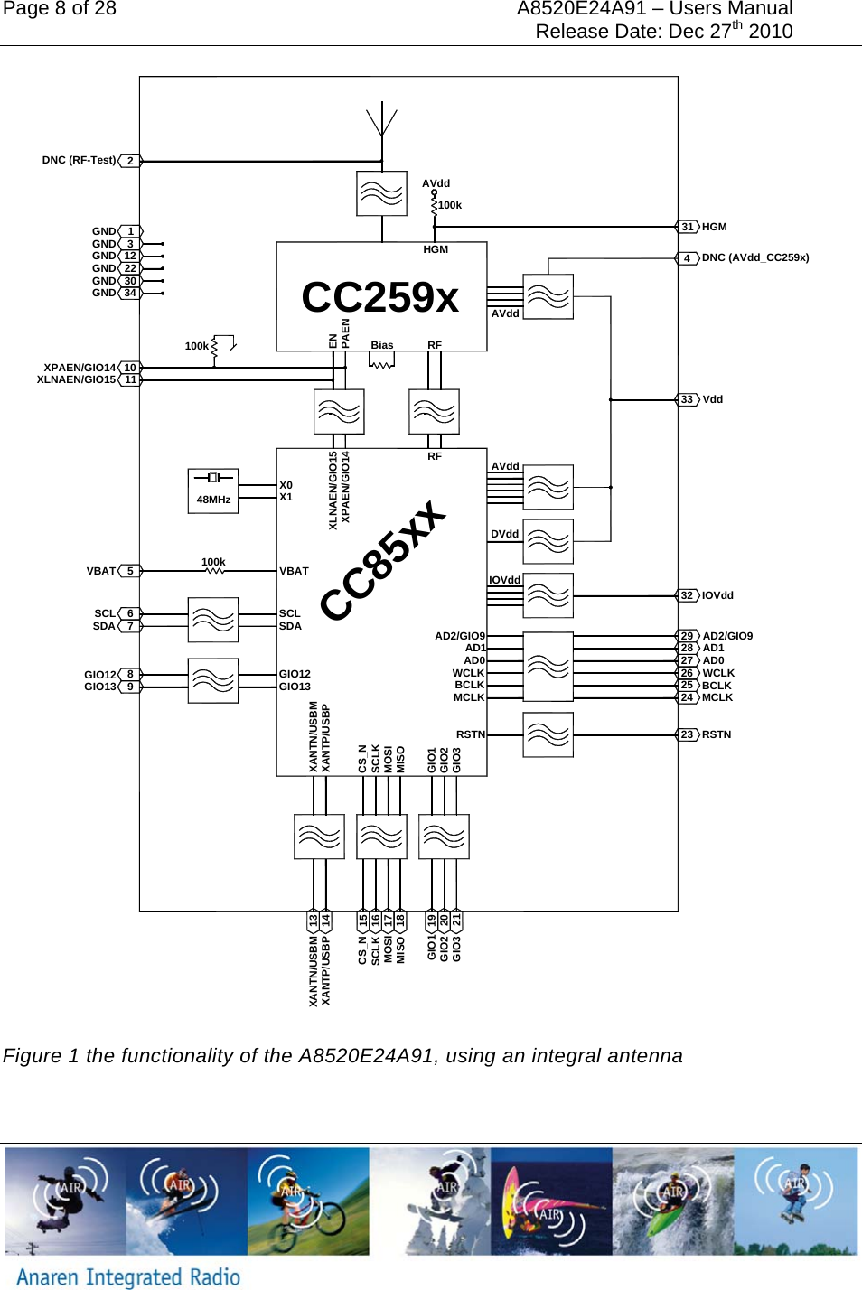

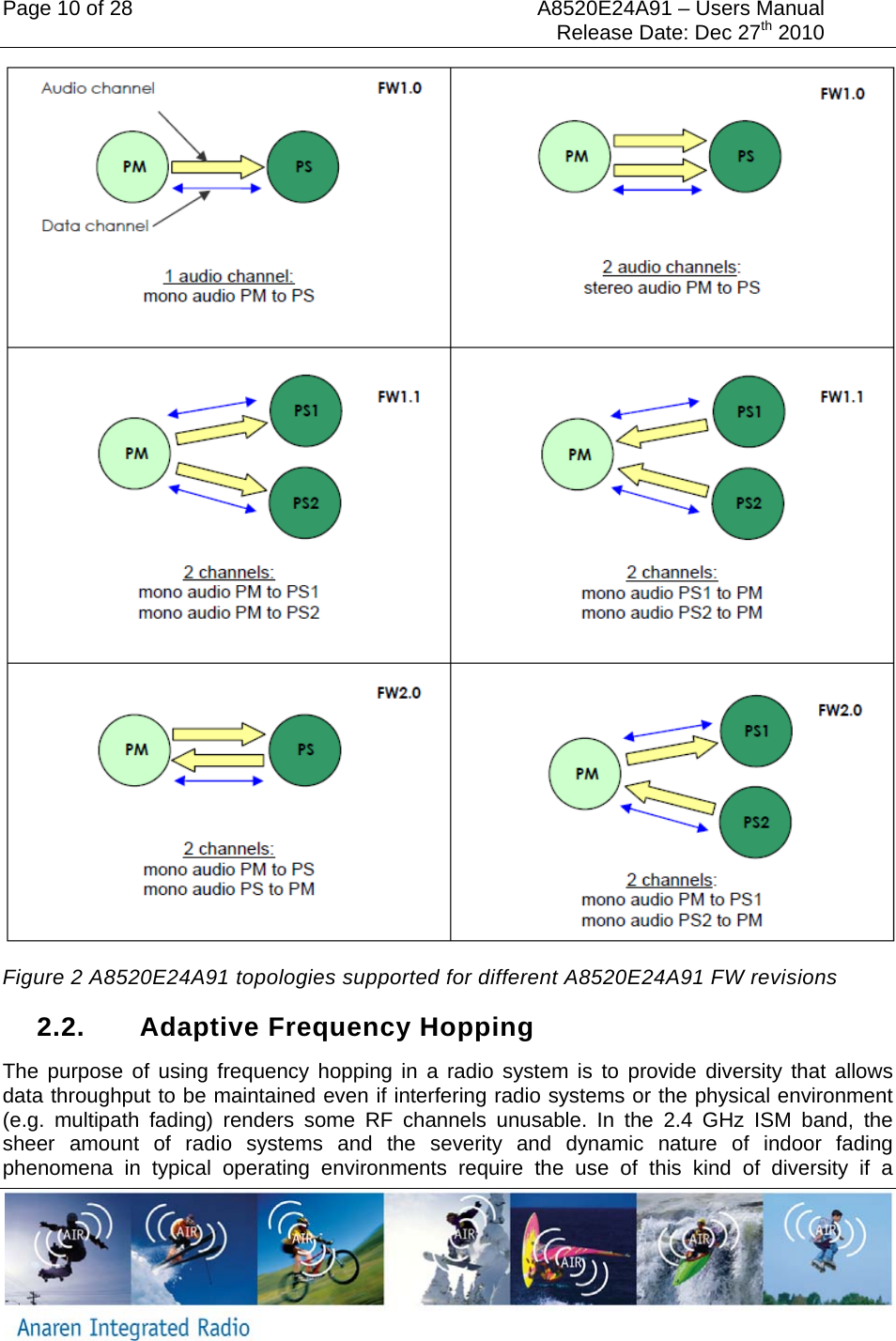
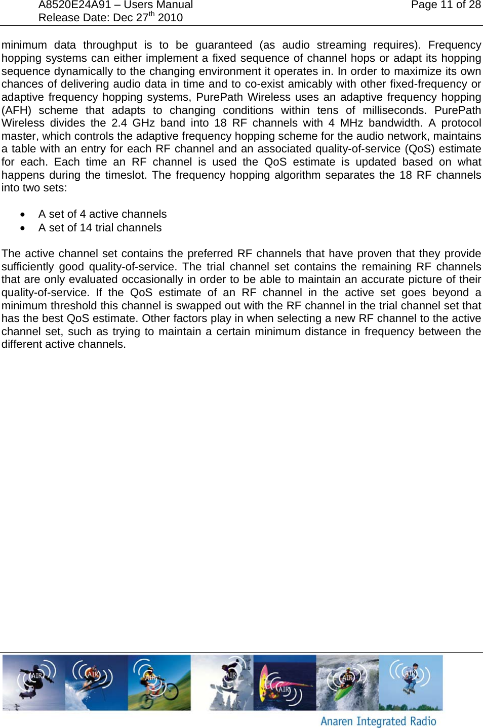
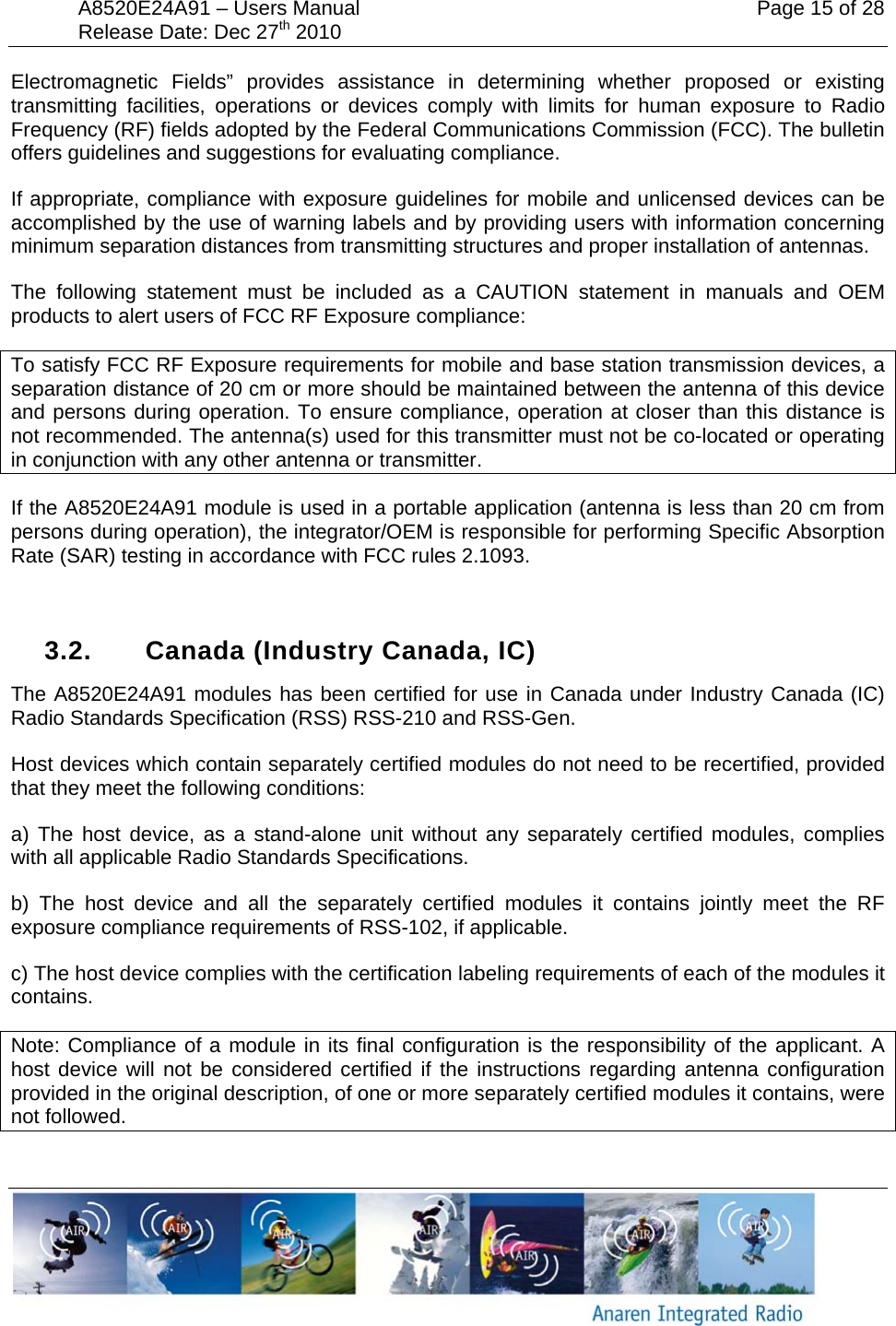
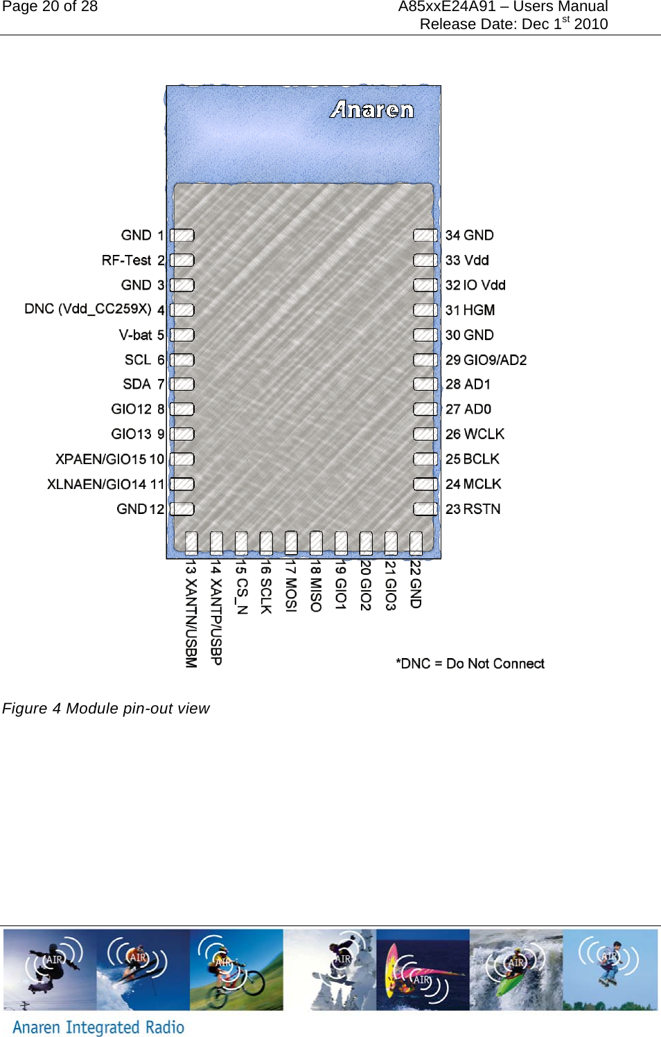
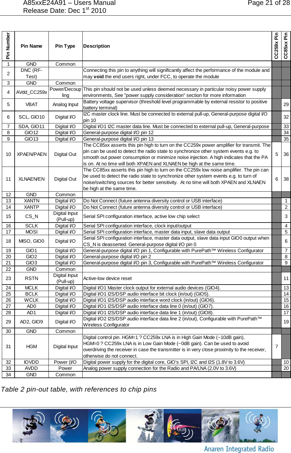
![Page 12 of 28 A8520E24A91 – Users Manual Release Date: Dec 27th 2010 Figure 3 Example of AFH hop sequence (active set in color, trial set in black/gray) The frequency hopping algorithm, when no swaps between the active and trial channel sets occur, goes through a sequence of 70 hops over the course of which every RF channel has been used. • This 70-hop macrosequence consists of 14 repetitions of a o 5-hop microsequence during which Each of the four active RF channels are used once One of the trial RF channels is used once (cycling through all trial channels over the course of a macrosequence) Figure 3 illustrates this concept. This gives an average steady-state RF channel usage in an audio network of: • Each of the four active channels are used 20% of the time • Each trial channel is used 1.43% of the time The channels correspond to center frequencies as follows: Channel Center Frequency [MHz] Channel Center Frequency [MHz] 1 2406 10 2442 2 2410 11 2446 3 2414 12 2450 4 2418 13 2454 5 2422 14 2458](https://usermanual.wiki/Anaren/A10051701/User-Guide-1397280-Page-12.png)
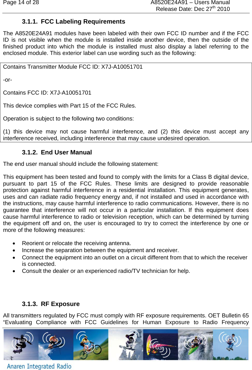
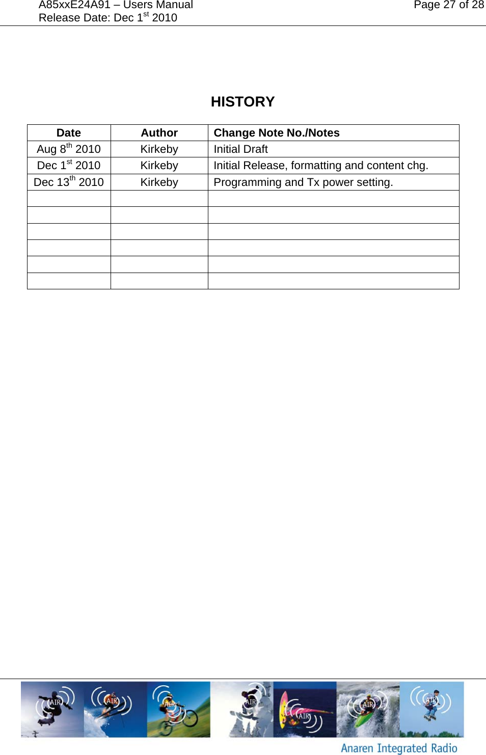
![Page 24 of 28 A85xxE24A91 – Users Manual Release Date: Dec 1st 2010 • Add decoupling capacitance to pin 33 (AVdd), 1uF to 2.2uF ceramic capacitor is suggested (do not use Tantalum). • Add a low noise LDO in the supply line to pin 33 (AVdd) (the TPS731xx low Dropout Regulator from TI is recommended). Note that if operated from a battery source there is no need for additional noise reduction. Also note that if the noise source can be synchronized to be off whenever the module is transmitting or receiving (using XPAEN and XLNAEN) then that will also suffice. 5. Configuration and Programming The integrator of this module into an application must program the module to match both the Codec chip used and the human interface methods employed. To do this the integrator must use the PurePath™ software from Texas Instruments to configure the module 5.1. Calibrating Transmit Power This power calibration number is an approximate power output value in dBm for the CC85xx chip – however the modules CC2591 adds an additional 16dB amplification. The maximum allowed setting to comply with FCC/IC is “0” (which produces 16dBm output power). Any setting above this voids the end users right to use the equipment. It can be useful to set a lower power for systems that do not require the full range and thus save on power consumption. The typical power consumption at 3.3v supply for a A8520E24A91 module is shown below depending on the output power setting. Output Power Setting Actual Output Power (Approximate) Current Consumption [mA] @ 3.3V AVdd,IOVdd, Ambient # [dBm] Master Slave 0 16 48 18 -1 15 43 18 -2 14 39 17 -3 13 38 17 -4 12 34 16 -5 11 33 16 -6 10 32 15 -7 9 32 15 -8 8 30 15 -9 7 28 15 -10 6 27 15 In the PurePathTM configurator when creating the application image, in the “Radio” page for both master and slave the target Tx power must be set to 0 dBm, or lower, (note that this produces 16dBm peak from the module due to CC2591 PA/LNA):](https://usermanual.wiki/Anaren/A10051701/User-Guide-1397280-Page-24.png)