AnyDATA DTEVDUAL cdma EVDO/1x Module User Manual CDMA DATA TERMINAL
AnyDATA Corporation cdma EVDO/1x Module CDMA DATA TERMINAL
UserManual.wiki
>
AnyDATA
>
DTEVDUAL User Manual
users manual
Navigation menu
Upload a User Manual
Namespaces
Wiki Guide
HTML
PDF
Info
Views
User Manual
Discussion / Help
Navigation
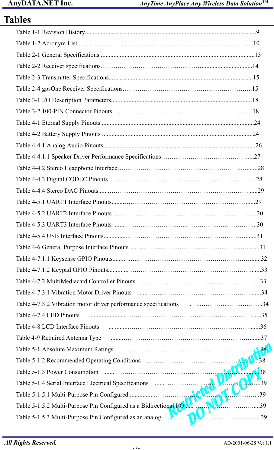
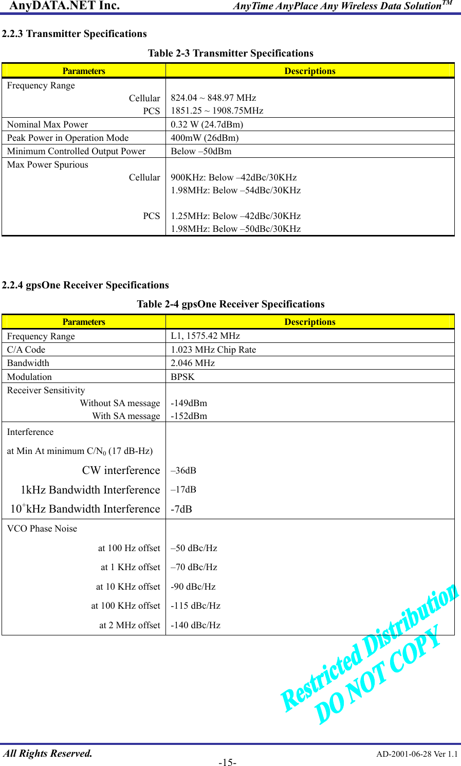
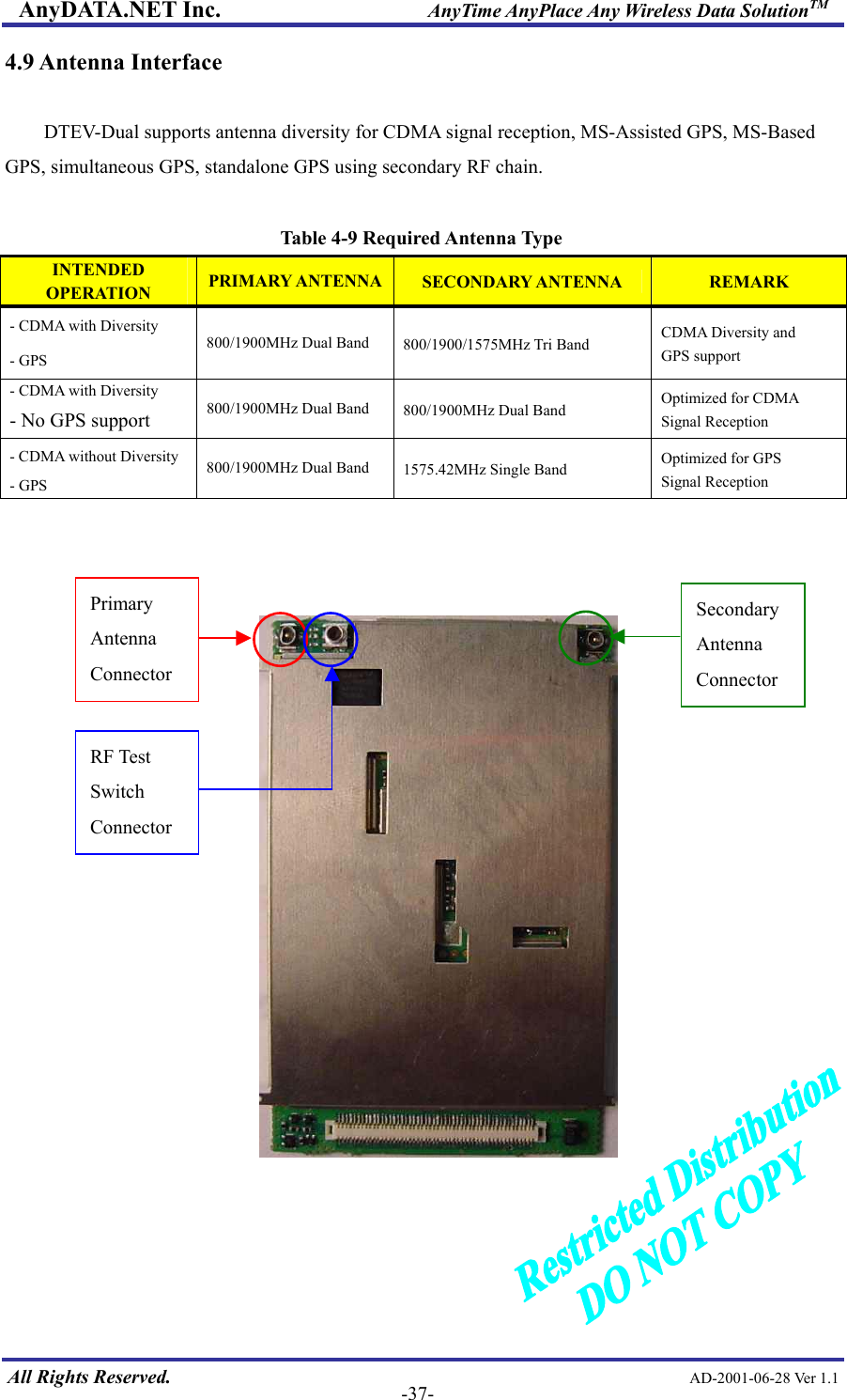
![AnyDATA.NET Inc. AnyTime AnyPlace Any Wireless Data SolutionTM 3. PIN Description 3.1 I/O Description Parameters Table 3-1 I/O Description Parameters Symbol Description I CMOS Input O Output B Bi-directional V Power/Ground IS Input with Schmitt Trigger BS Bi-directional Schmitt Trigger PU Internal Pull-Up PD Internal Pull-Down 3.2 PIN Names and Pinouts 3.2.1 100-Pin Connector Table 3-2 100-PIN Connector Pinouts All Rights Reserved. AD-2001-06-28 Ver 1.1 -18-Pin # Name Main Function Dir-Pol Description 1 D2[15] EBI2_DATA15 B peripheral data bus 2 GND GROUND V Signal Ground 3 D2[14] EBI2_DATA14 B peripheral data bus 4 GND GROUND V Analog Ground 5 D2[12] EBI2_DATA12 B peripheral data bus 6 D2[13] EBI2_DATA13 B peripheral data bus 7 D2[10] EBI2_DATA10 B peripheral data bus 8 D2[11] EBI2_DATA11 B peripheral data bus 9 D2[08] EBI2_DATA08 B peripheral data bus 10 D2[09] EBI2_DATA09 B peripheral data bus 11 GND GROUND V Signal ground 12 GND GROUND V Signal ground 13 GPIO_39 UART1_DCD_N O Data carrier detect ( UART1 ) 14 GPIO_64 UART1_RI_N O Ring indicator ( UART1 ) 15 GPIO_98 UART1_RFR_N O Ready for Receive ( UART1 ) same as RTS 16 GPIO_95 UART1_TXD O Transmit data ( UART1 ) 17 GPIO_44 UART1_DTR I Data terminal ready ( UART1 ) 18 GPIO_96 UART1_RXD I Receive data ( UART1 )](https://usermanual.wiki/AnyDATA/DTEVDUAL/User-Guide-624254-Page-18.png)
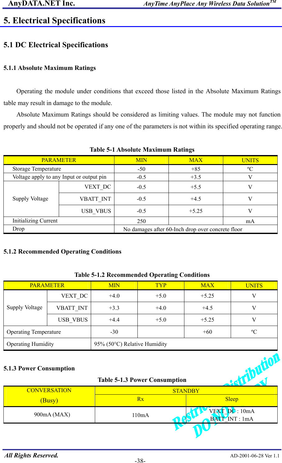
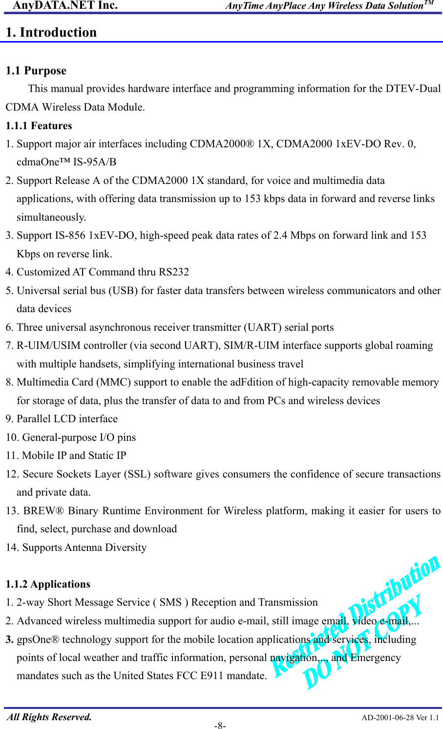
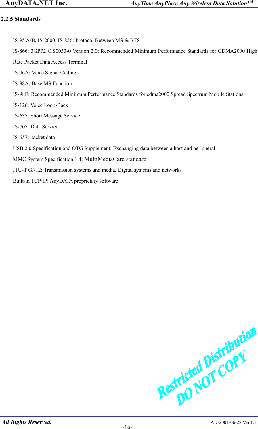
![AnyDATA.NET Inc. AnyTime AnyPlace Any Wireless Data SolutionTM All Rights Reserved. AD-2001-06-28 Ver 1.1 -19-19 GPIO_97 UART1_CTS_N I Clear to send ( UART1 ) 20 VREG_UIM VREG_RUIM O +3V power supply to RUIM caed 21 UIM_P_DATA UIM_P_DATA I Data from RUIM card 22 UIM_P_RESET UIM_P_RESET O RUIM card reset 23 UIM_P_CLK UIM_P_CLK O RUIM clock 24 MMC_DATA MMC_DATA B GPIO_32, MultiMediaCard data 25 MMC_CLK MMC_CLK B GPIO_31, MMC clock 26 GPIO_84 UART3_TXD O transmit data, (UART3) DEBUG PORT 27 MMC_CMD MMC_CMD B GPIO_30, MMC command 28 GPIO_85 UART3_RXD I receive data, (UART3) DEBUG PORT 29 VREG_MMC VREG_AUX1 O Linear regulator output intended to power MMC circuits 30 POWER_ON POWER_ON I POWER ON used only when to use 3.6V 1cell battery. External pull-up required 31 GPIO_24 LCD_LED_CONT O General purpose input output, LCD LED 32 GPIO_13 FLASH_LED_CONT O General purpose input output, FLASH LED 33 GPIO_17 GPIO_17 B General purpose input output 34 VREG_MSME VREG_MSME O Regulated output of the MSME buck (step-down) SMPS 35 VREG_AUX2 VREG_AUX2 O Low dropout linear regulator output intended to power WLAN 36 GND GROUND V Signal ground 37 GND GROUND V Signal ground 38 D2[00] EBI2_DATA00 B Data line 39 D2[01] EBI2_DATA01 B Data line 40 D2[02] EBI2_DATA02 B Data line 41 D2[03] EBI2_DATA03 B Data line 42 D2[04] EBI2_DATA04 B Data line 43 D2[05] EBI2_DATA05 B Data line 44 D2[06] EBI2_DATA06 B Data line 45 D2[07] EBI2_DATA07 B Data line 46 A2[20] A2[20] O Address line 47 A2[01] A2[01] O Address line 48 RESOUT1 RESOUT1_N O Reset Out 49 LCD2_CS LCD2_CS_N O Peripheral LCD chip select 50 GPIO23 LED_FULL_CURRENT O GPIO, Full Current LED](https://usermanual.wiki/AnyDATA/DTEVDUAL/User-Guide-624254-Page-19.png)

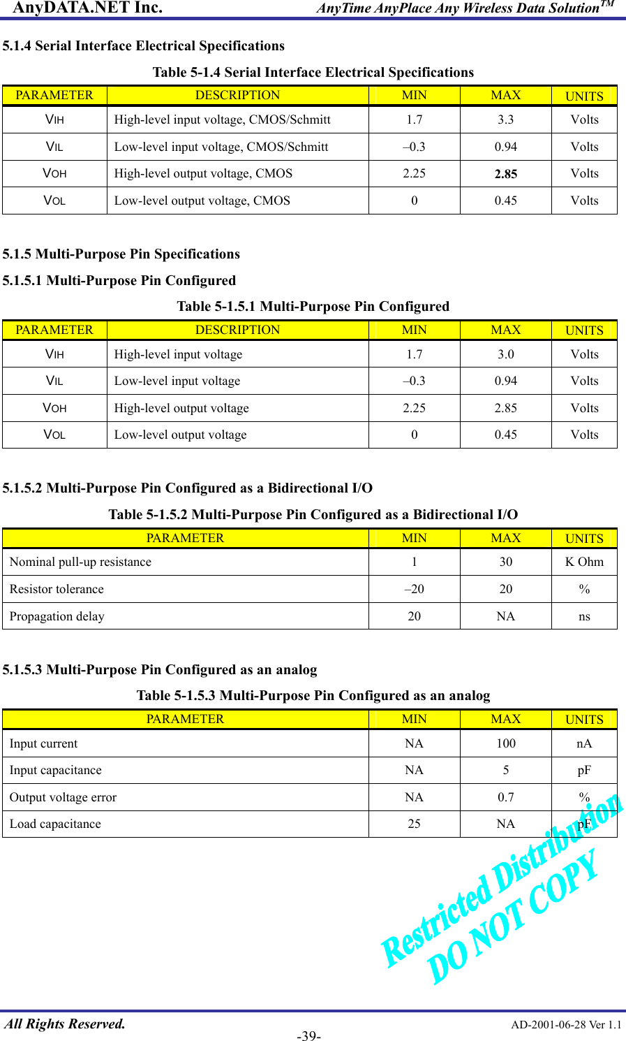
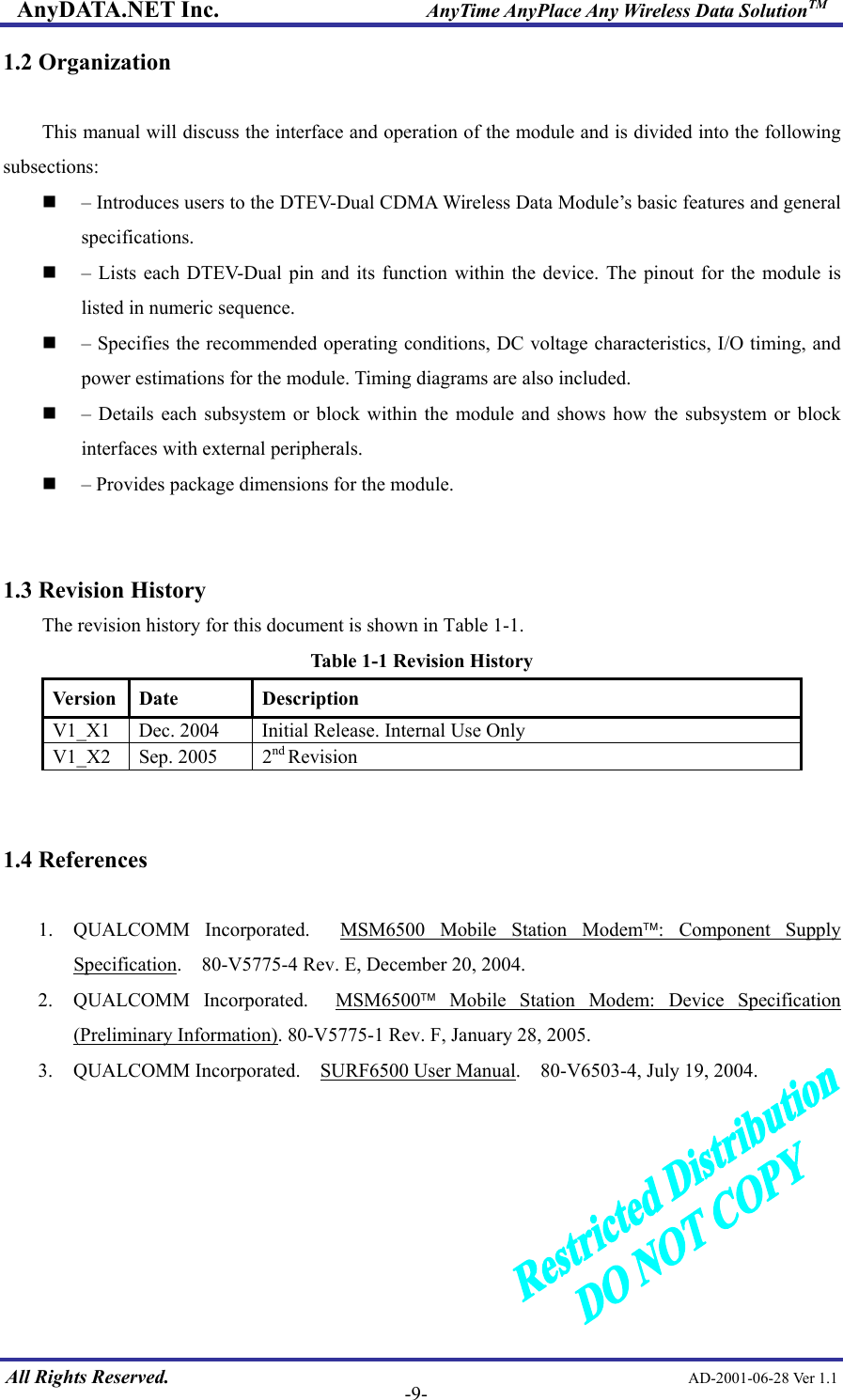
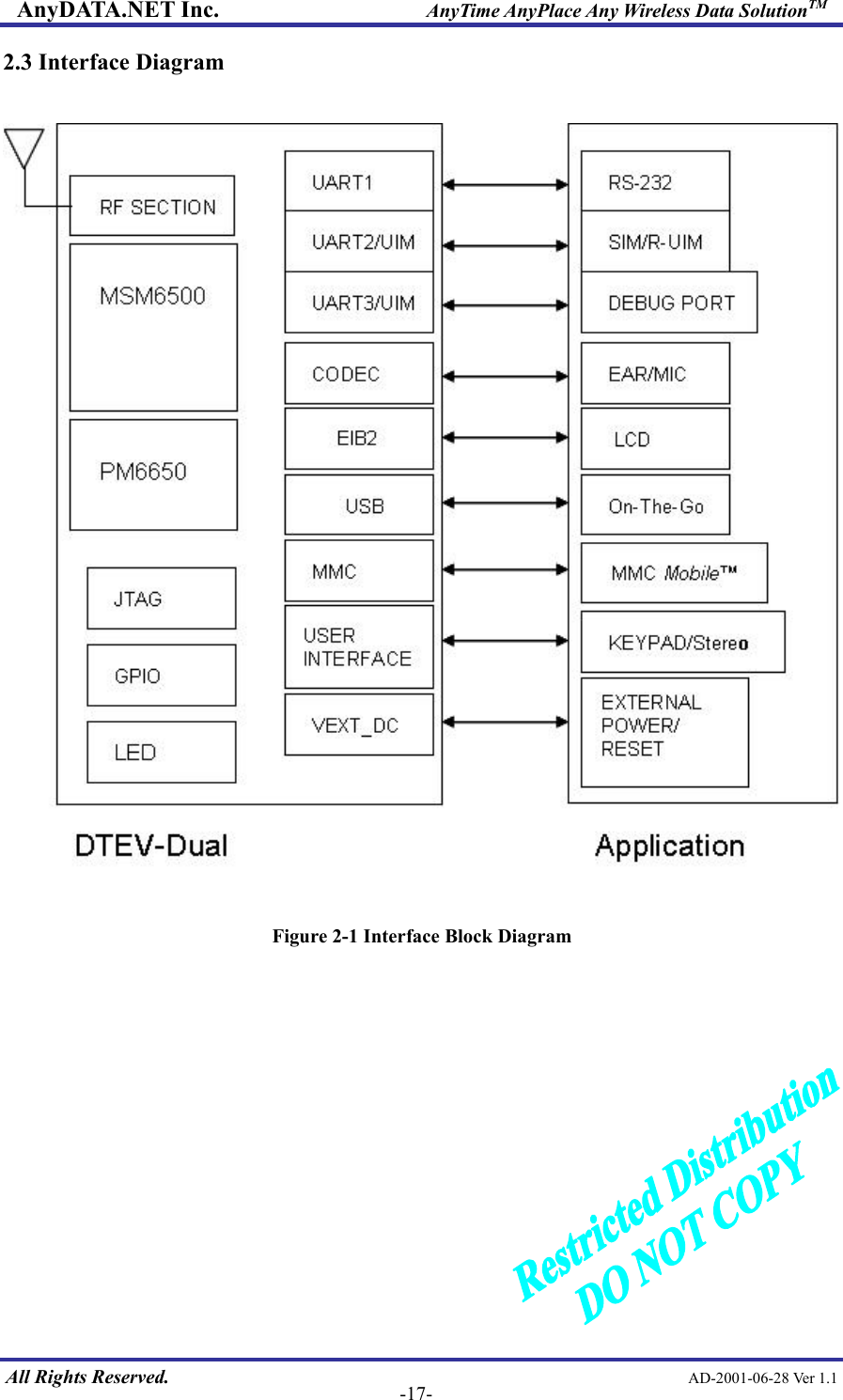
![AnyDATA.NET Inc. AnyTime AnyPlace Any Wireless Data SolutionTM 4.7 User Interface 4.7.1 Keypad The keypad interface consists of a 5 X 6 matrix pattern. The 5-KEYSENSE/[4:0] pins are used to connect a matrix keypad to the module. The KEYSENSE/ pins are active low. The 6-KEYPAD pins are necessary to construct the other side of the matrix. These KEYPAD pins must be active high in order for the keypad matrix to work properly. The general keypad matrix is shown below: 3 2 1 6 5 4 9 8 7 END # 0 * SEND KEYSENSE0 KEYSENSE1 KEYSENSE2 KEYSENSE3 KEYPAD00 KEYPAD01 KEYPAD02 KEYPAD03 KEYPAD04 KEYPAD05 Figure 4-7.1 Keypad Matrix Reserved Table 4-7.1.1 Keysense GPIO Pinouts Pin # Pin Name Main Function Type Description 53 GPIO_62 KEYSENSE0_N I Key sense input 54 GPIO_63 KEYSENSE1_N I Key sense input 55 GPIO_46 KEYSENSE2_N I Key sense input 56 GPIO_47 KEYSENSE3_N I Key sense input 57 GPIO_48 KEYSENSE4_N I Key sense input All Rights Reserved. AD-2001-06-28 Ver 1.1 -32-](https://usermanual.wiki/AnyDATA/DTEVDUAL/User-Guide-624254-Page-32.png)
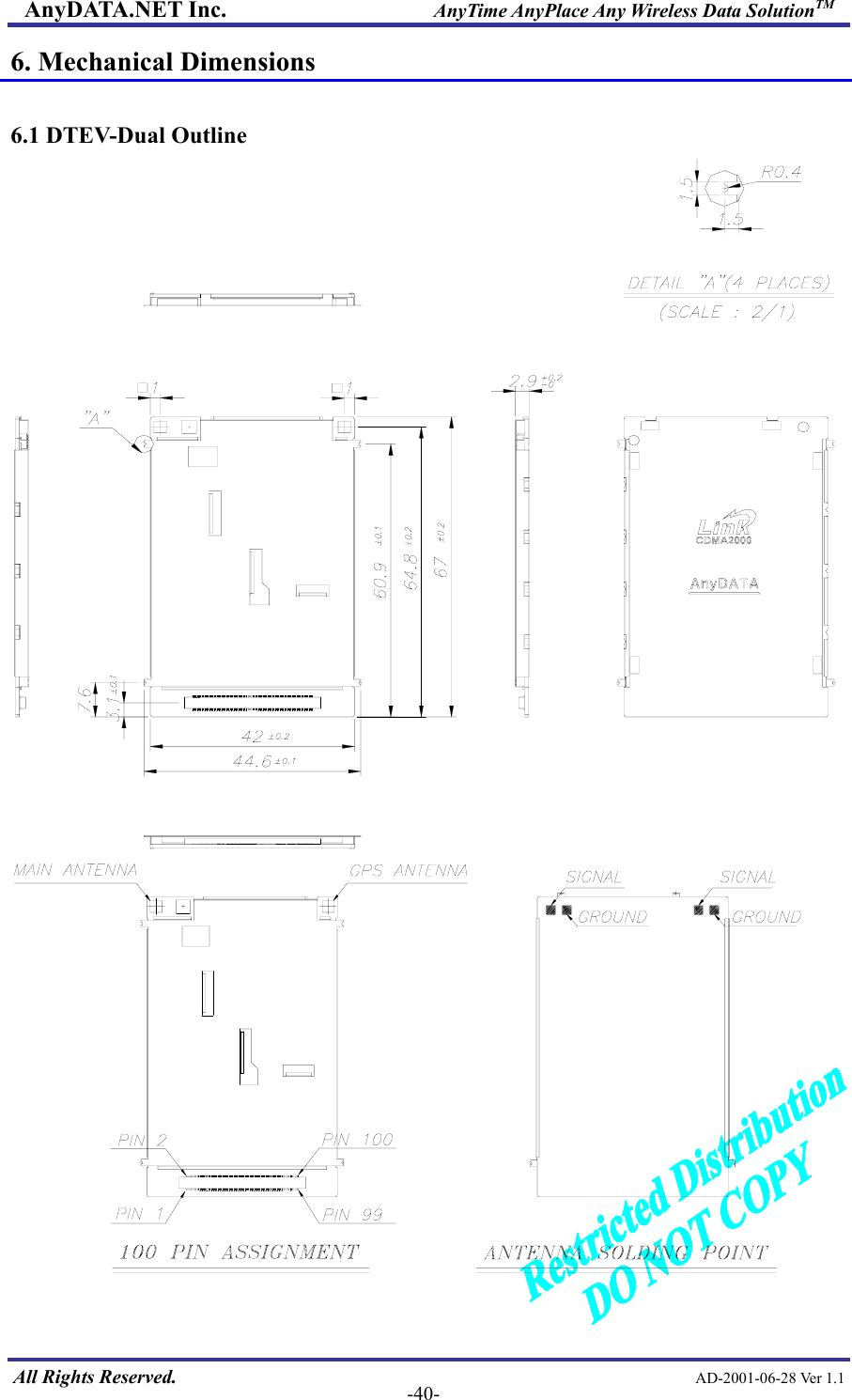
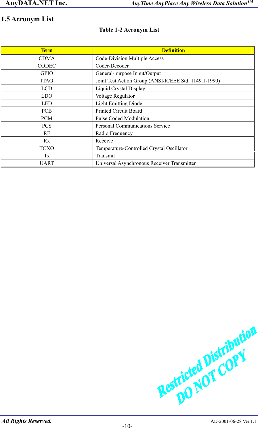
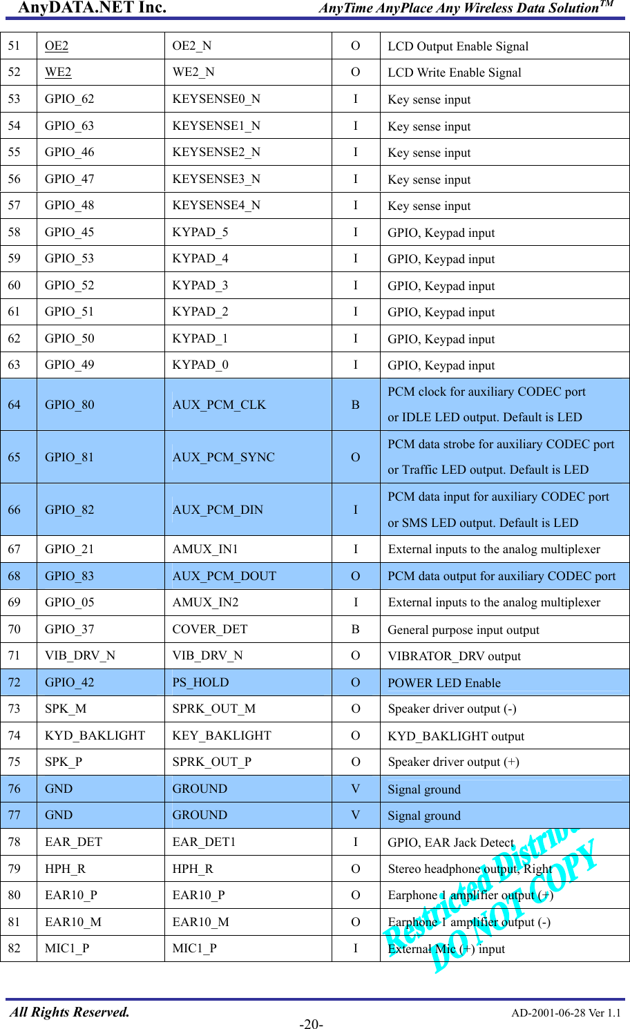
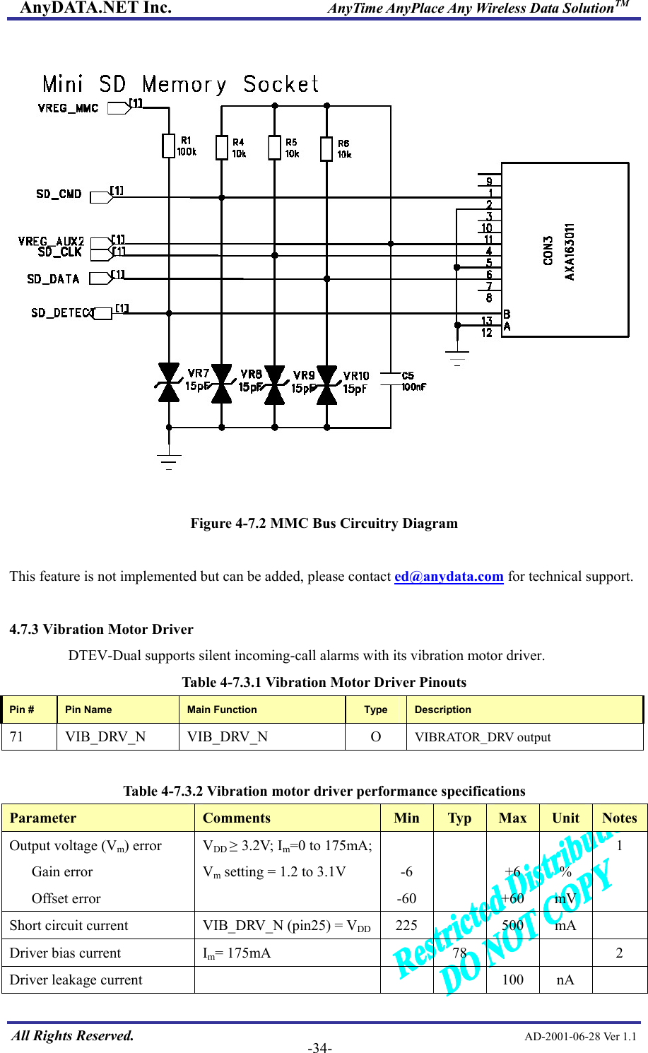
![AnyDATA.NET Inc. AnyTime AnyPlace Any Wireless Data SolutionTM Table 4-7.1.2 Keypad GPIO Pinouts Pin # Pin Name Main Function Type Description 58 GPIO_45 KYPAD_5 I GPIO, Keypad input 59 GPIO_53 KYPAD_4 I GPIO, Keypad input 60 GPIO_52 KYPAD_3 I GPIO, Keypad input 61 GPIO_51 KYPAD_2 I GPIO, Keypad input 62 GPIO_50 KYPAD_1 I GPIO, Keypad input 63 GPIO_49 KYPAD_0 I GPIO, Keypad input DTMF When key is pressed, CDMA Module generates standard DTMF tone and sends it to the local audio path (speaker). If the Mobile station is in traffic state, the CDMA Module sends DTMF Message to the Base Station and to the local audio path (speaker) at the same time. The network will deliver the analog DTMF tone or DTMF Message to its final destination. This feature is not implemented but can be added, please contact ed@anydata.com for technical support. . 4.7.2 MultiMediaCard controller DTEV-Dual contains a MultiMediaCard (MMC) controller that provides a link between the ARM bus master and the MultiMediaCard bus for storing digital music, games, address books and photos. The SD card supports a 1-bit SD bi-directional bus mode. SD bus pins are CLK, CMD and DAT in 1-bit mode and CLK, CMD, and DAT[0:3] in 4-bit mode. The MultiMediaCard also supports the 1-bit bi-directional MMC bus mode that has CLK, CMD, and DAT bus pins. The CMD and DAT pins are bi-directional on the SD 1-bit, SD 4-bit, and MMC 1-bit. DTEV-Dual can’t support SD 4-bit mode. MMC version 3.31 is supported for the ROM class and R/W MMCs. SD Memory Card Physical Layer Specification Version 1.01 is supported in SD bus mode. Table 4-7.2 MultiMediacatd Controller Pinouts All Rights Reserved. AD-2001-06-28 Ver 1.1 -33-Pin # Pin Name Main Function Type Description 24 MMC_DATA MMC_DATA B GPIO_32, MultiMediaCard data 25 MMC_CLK MMC_CLK O GPIO_31, MMC clock 27 MMC_CMD MMC_CMD B GPIO_30, MMC command 29 VREG_MMC VREG_MMC O +2.85V 35 VREG_AUX2 VREG_AUX2 O +2.85V 68 GPIO_INT22 SD_DETECT I SD/MMC detect. Low detection](https://usermanual.wiki/AnyDATA/DTEVDUAL/User-Guide-624254-Page-33.png)
![AnyDATA.NET Inc. AnyTime AnyPlace Any Wireless Data SolutionTM 4.8 External Bus Interface II ( or LCD Interface ) The External bus interface II supports the parallel LCD interfaces. The port mapped or memory mapped (16-bit interface and 8-bit devices) parallel LCD device could be connected to chip select LCD2_CS_N in EBI2. The maximum address space per chip select is 2 Megabyte. Direct access to the LCD driver is not applicable. Table 4-8 LCD Interface Pinouts Pin # Pin Name Main Function Type Description 1 D2[15] EBI2_DATA15 B Data line 3 D2[14] EBI2_DATA14 B Data line 5 D2[12] EBI2_DATA12 B Data line 6 D2[13] EBI2_DATA13 B Data line 7 D2[10] EBI2_DATA10 B Data line 8 D2[11] EBI2_DATA11 B Data line 9 D2[08] EBI2_DATA08 B Data line 10 D2[09] EBI2_DATA09 B Data line 38 D2[00] EBI2_DATA00 B Data line 39 D2[01] EBI2_DATA01 B Data line 40 D2[02] EBI2_DATA02 B Data line 41 D2[03] EBI2_DATA03 B Data line 42 D2[04] EBI2_DATA04 B Data line 43 D2[05] EBI2_DATA05 B Data line 44 D2[06] EBI2_DATA06 B Data line 45 D2[07] EBI2_DATA07 B Data line 46 A2[20] A2[20] O Address line 47 A2[01] A2[01] O Address line 49 LCD2_CS LCD2_CS_N O 48 RESOUT1 RESOUT1_N O Reset Out 51 OE2 OE2_N O Output Enable Signal 52 WE2 WE2_N O Write Enable Signal Peripheral LCD Chip Select This feature is not implemented but can be added, please contact ed@anydata.com for technical support. All Rights Reserved. AD-2001-06-28 Ver 1.1 -36-](https://usermanual.wiki/AnyDATA/DTEVDUAL/User-Guide-624254-Page-36.png)