AnyDATA DTG2000 CDMA Data Module User Manual 01 DTG2000 Dual 1 X5
AnyDATA Corporation CDMA Data Module 01 DTG2000 Dual 1 X5
UserManual.wiki
>
AnyDATA
>
DTG2000 User Manual
Users Manual
Navigation menu
Upload a User Manual
Namespaces
Wiki Guide
HTML
PDF
Info
Views
User Manual
Discussion / Help
Navigation
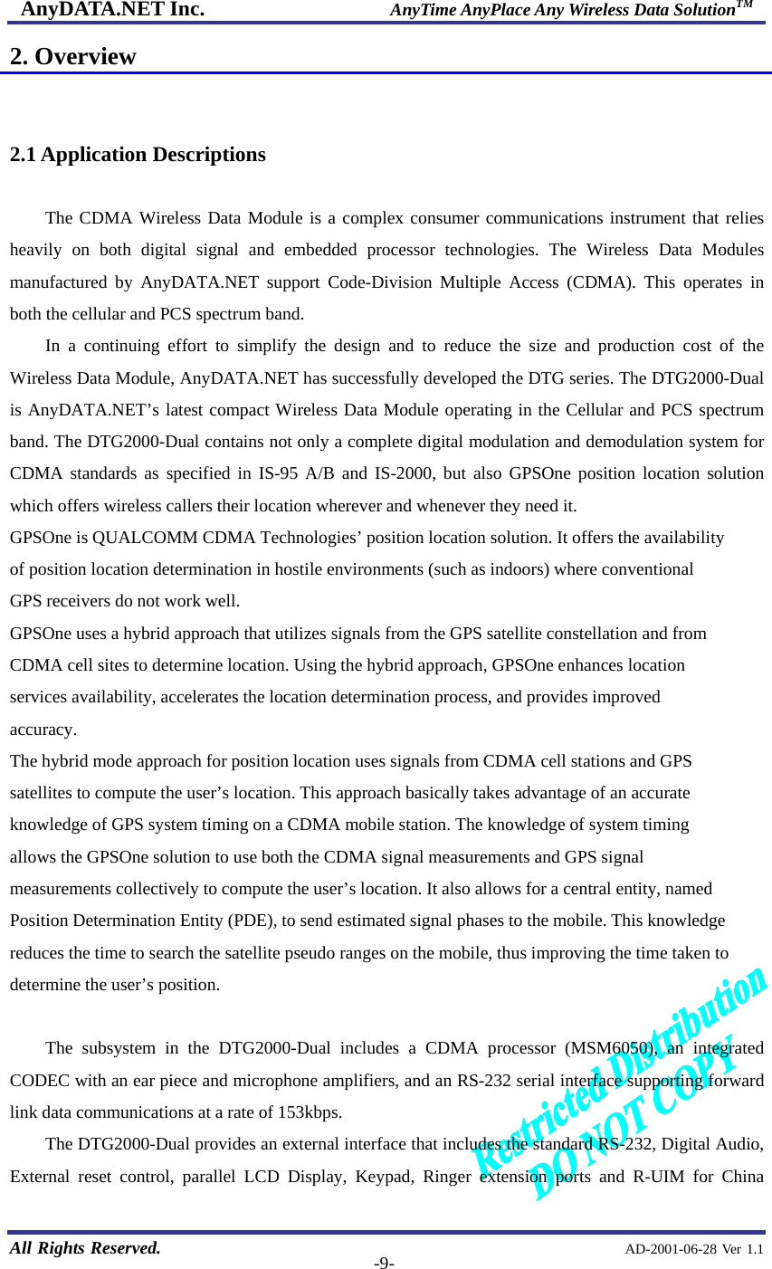
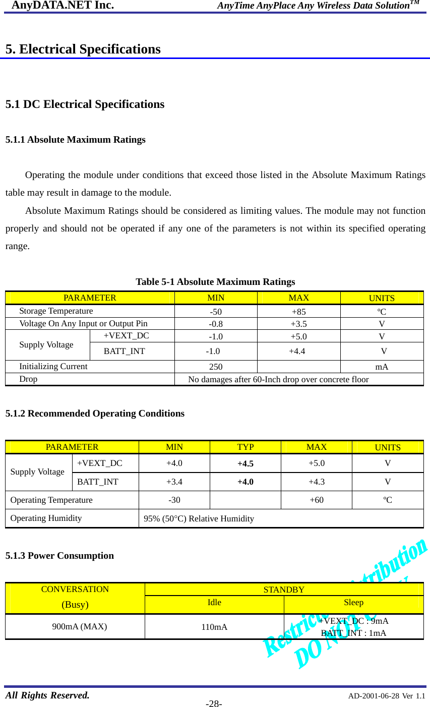
![AnyDATA.NET Inc. AnyTime AnyPlace Any Wireless Data SolutionTM All Rights Reserved. AD-2001-06-28 Ver 1.1 -25-4.7 User Interface 4.7.1 Keypad The keypad interface consists of a 5 X 6 matrix pattern. The 5-KEYSENSE/[4:0] pins are used to connect a matrix keypad to the module. The KEYSENSE/ pins are active low. The 6-KEYPAD pins are necessary to construct the other side of the matrix. These KEYPAD pins must be active high in order for the keypad matrix to work properly. The general keypad matrix is shown below: Figure 4-1 Keypad Matrix DTMF When key is pressed, CDMA Module generates standard DTMF tone and sends it to the local audio path (speaker). If the Mobile station is in traffic state, the CDMA Module sends DTMF Message to the Base Station and to the local audio path (speaker) at the same time. The network will deliver the analog DTMF tone or DTMF Message to its final destination. KEYSENSE0KEYSENSE1KEYSENSE2KEYSENSE3KEYPAD00KEYPAD01KEYPAD02KEYPAD03KEYPAD04#0*SEND98 7END65 432 1ReservedKEYPAD05KEYSENSE4](https://usermanual.wiki/AnyDATA/DTG2000/User-Guide-449729-Page-25.png)
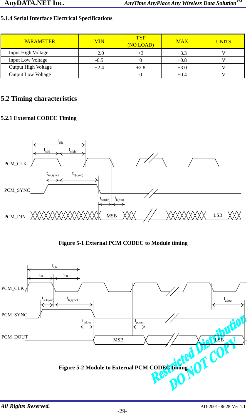
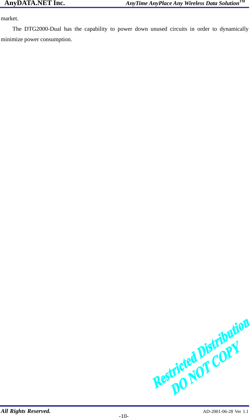
![AnyDATA.NET Inc. AnyTime AnyPlace Any Wireless Data SolutionTM All Rights Reserved. AD-2001-06-28 Ver 1.1 -30-Table 5-2 External PCM CODEC Parameters PARAMETER DESCRIPTION MIN TYP. MAX UNIT tclk PCM-CLK cycle time 400 500 ns tclkl PCM-CLK low time 200 250 ns tclkh PCM-CLK high time 200 250 ns tsu(sync) PCM_SYNC setup time to PCM_CLK falling 150 ns th(sync) PCM_SYNC hold time after PCM_CLK falling 350 ns tsu(din) PCM_DIN setup time to PCM_CLK falling 50 ns th(din) PCM_DIN hold time after PCM_CLK falling 10 ns tpdout Delay from PCM_CLK falling to PCM_DOUT 50 ns 5.2.2 LCD Timing tWRSMCLK(modem)A[21:0]LWR/WriteData[7:0]LCD_CS/RD/LCD_EReadData[7:0]TtWRHtLCDEStLCDEHItLCDEHtRDStRDHLCD Data WriteLCD Data Read Figure 5-3 LCD Timing](https://usermanual.wiki/AnyDATA/DTG2000/User-Guide-449729-Page-30.png)