AnyDATA DTS-800CDK CDMA Development kit DTS-800 User Manual Service manual
AnyDATA Corporation CDMA Development kit DTS-800 Service manual
UserManual.wiki
>
AnyDATA
>
DTS-800CDK User Manual
>
Service manual
Contents
1.
Service manual
2.
User Manual
Service manual
Navigation menu
Upload a User Manual
Namespaces
Wiki Guide
HTML
PDF
Info
Views
User Manual
Discussion / Help
Navigation
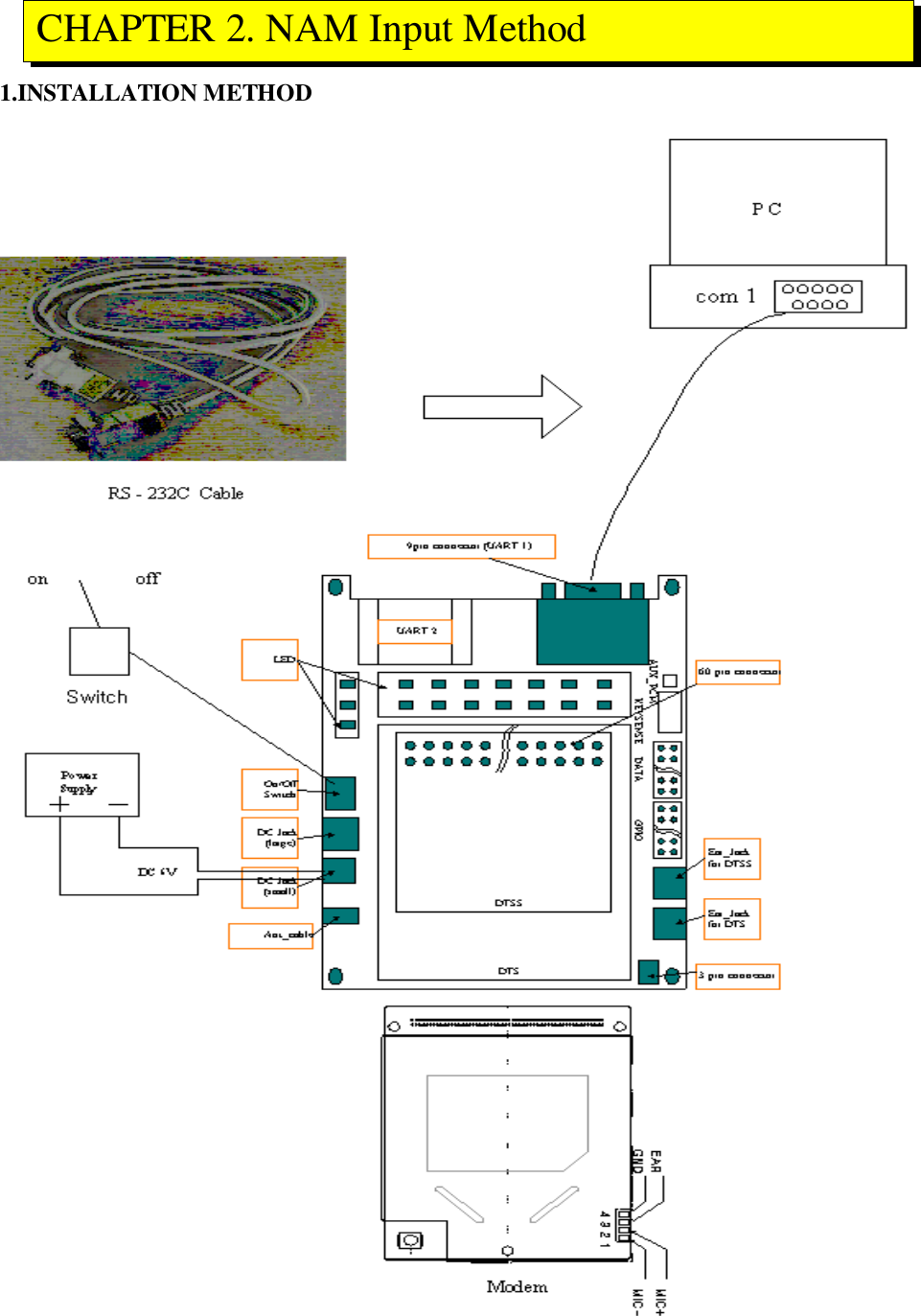
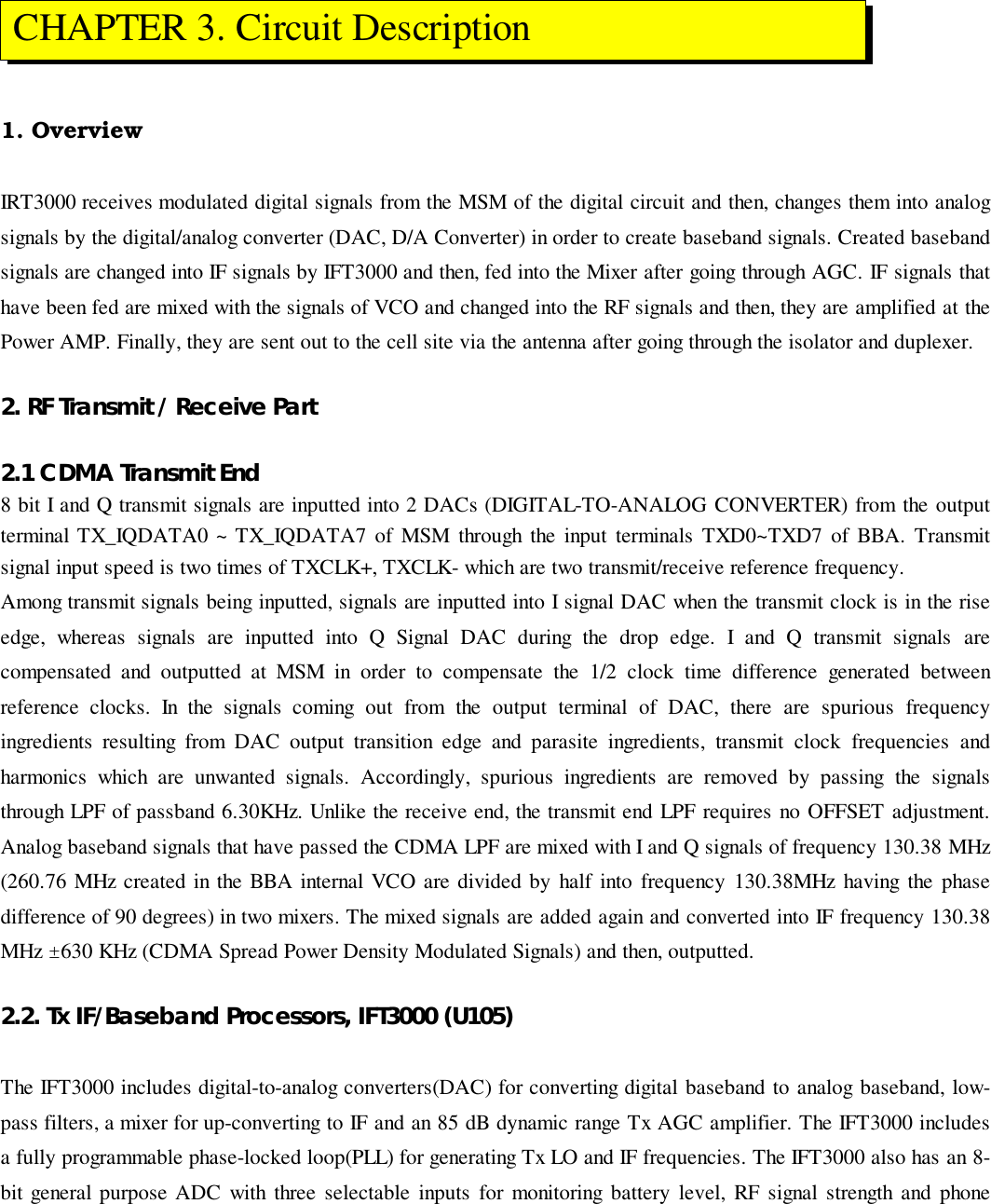
![1) Connect the MODEM to 60pin connector of Level Translator.2) Supply the voltage of 5~7V to small or large jack of Level Translator.3) Switch the power on.4) Connect the UART1 to PC COM1 port with the RS-232C cable.5) Install the operating program.2. OPERATION METHOD2) Set Buad rate to the modem’s.3) Click [DM mode]1) Run PSTDM program at Windows95 or Windows98](https://usermanual.wiki/AnyDATA/DTS-800CDK.Service-manual/User-Guide-221761-Page-15.png)
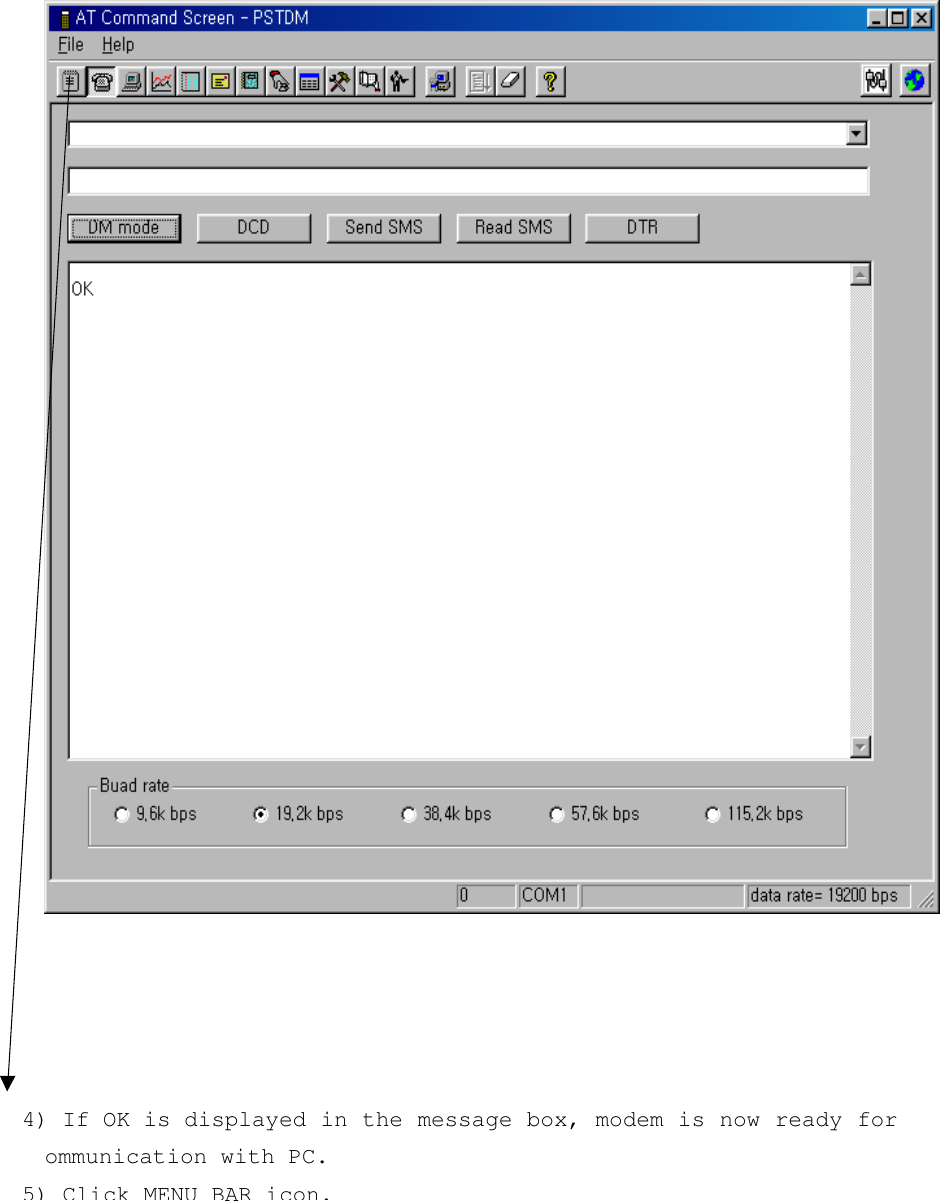
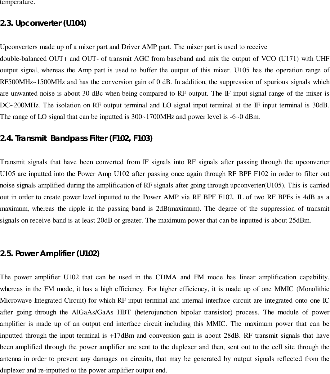
![6) As shown in the picture above, service file input plane will be displayed(See if clock is running. If it isn’t, communication with PC is notactivated. Repeat step 1 through 5, or reset the power of modem and repeat step 1through 5)7) Type NAM Programming script like the example shown below, <NAM Programming script example>Mode offline-d [ENTER]nv_write name_nam {0," AnyDATA telecom "} [ENTER]nv_write name_nam {1," AnyDATA telecom "} [ENTER]Mode reset [ENTER]SCRIPTINPUT WINDOW](https://usermanual.wiki/AnyDATA/DTS-800CDK.Service-manual/User-Guide-221761-Page-17.png)
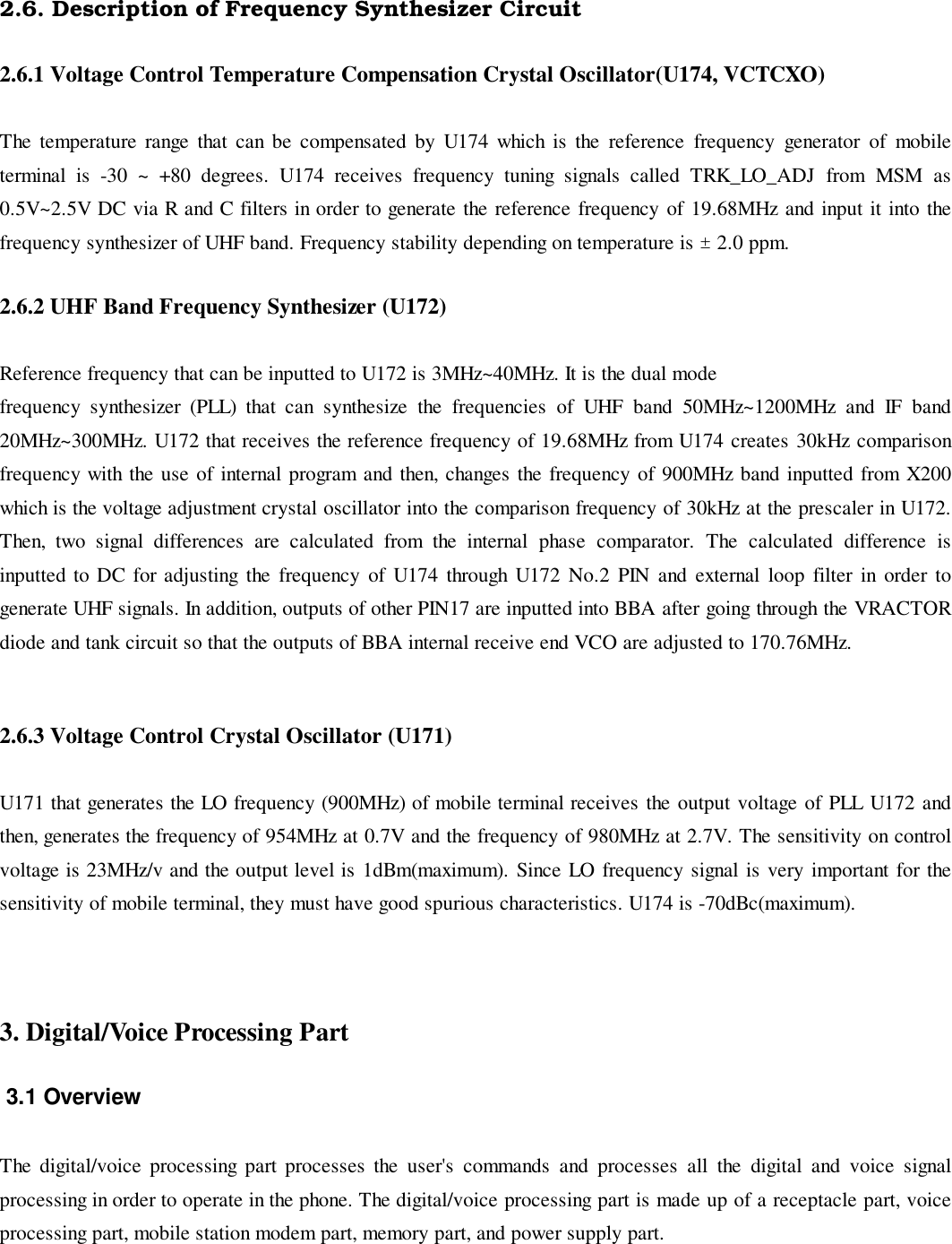
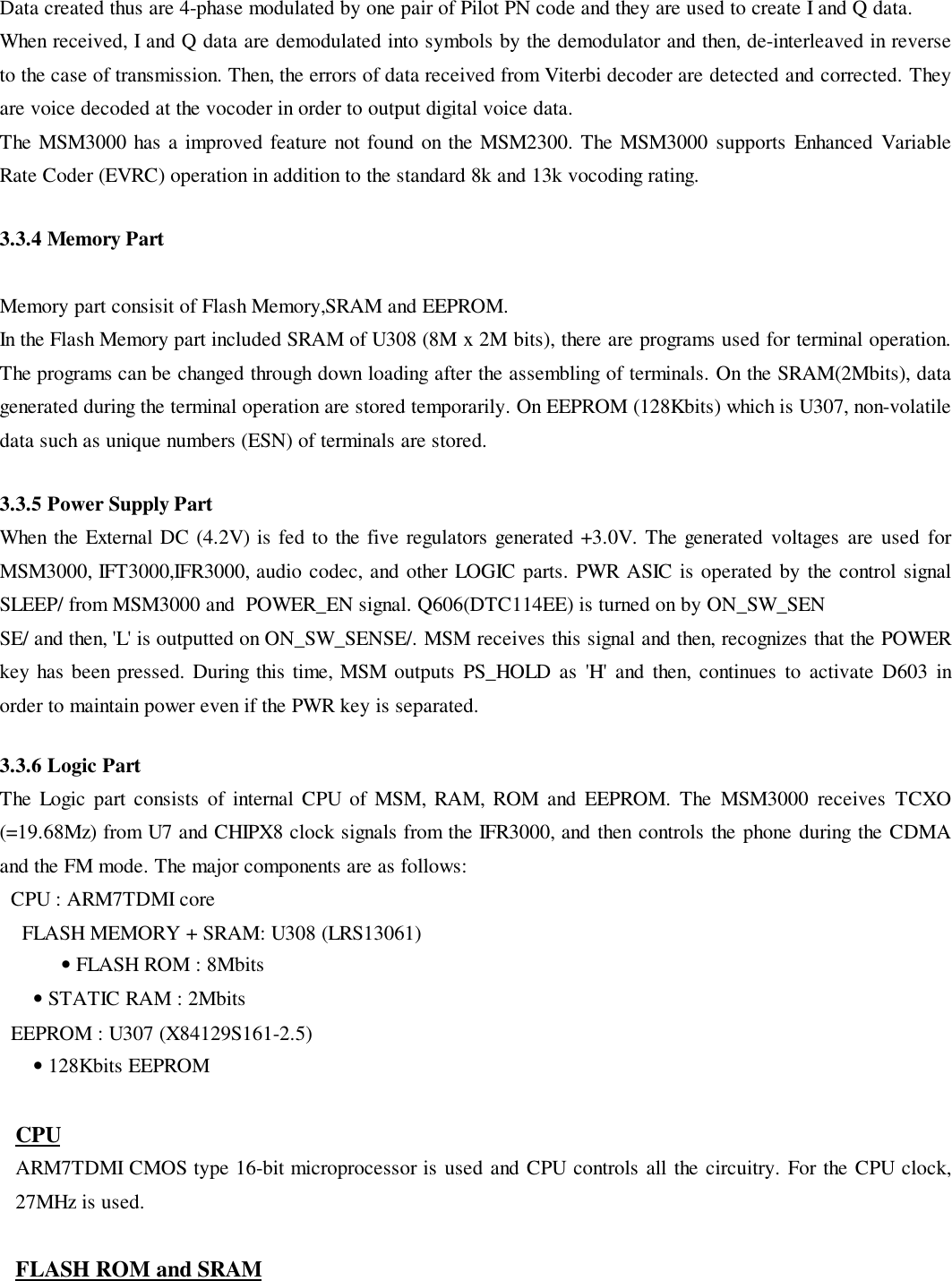
![Ringer FLASH Memory & SRAM EEPROM Receptacle Power Supply AUDIO Processor M SM300 0Earpiece Mic [Figure 3-1] Block Diagram of Digital/Voice Processing Part3.3.2 Audio Processing PartMIC signals are amplified through the audio codec which is U401 (TWL1103), and converted into digital signals.Then, they are inputted into MSM3000. In addition, digital audio signals outputted from MSM3000 are convertedinto analog signals after going through the audio codec to be amplified. and then transferred to the ear piece.3.3.3 MSM PartMSM3000, which is U301, is the core element of CDMA system terminal that includes ARM7TDMImicroprocessor core. It is made up of a CPU, encoder, interleaver, deinterleaver, Viterbi decoder, MOD/DEM, andvocoder. MSM3000, when operated in the CDMA mode, utilizes CHIPX8 (9.8304MHz) as the reference clock thatis received from IFR3000, and uses TCXO (19.68MHz) that is received from U174. CPU controls the terminaloperation. Digital voice data that have been inputted are voice-encoded and variable-rated. Then, they areconvolutionally encoded so that error detection and correction are possible. Coded symbols are interleaved in orderto cope with multi-path fading. Each data channel is scrambled by the long code PN sequence of the user in order toensure the confidentiality of calls.Moreover, binary quadrature codes are used based on Walsh functions in order to discern each channel.](https://usermanual.wiki/AnyDATA/DTS-800CDK.Service-manual/User-Guide-221761-Page-22.png)
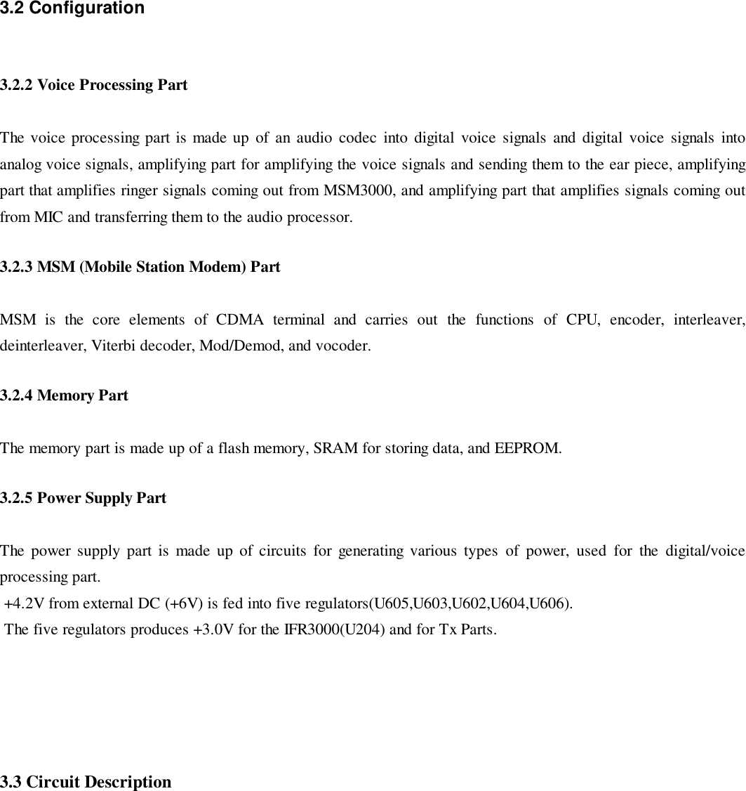
![Flash ROM is used to store the terminal’s program. Using the down-loading program, the program can be changedeven after the terminal is fully assembled.SRAM is used to store the internal flag information, call processing data, and timer data.4. Level Translator Part4.1 L/T supply power to Modem(4.2V).DC/Jack(small)DC/Jack(large)Adjustable LDOVEXT_DC+4.2VFixedLDO+5Vmax(207) [Fig 4-1] The Block Diagram of Source (in brief)4.2 UART InterfaceThe Universal Asynchronous Receiver Transmitter (UART) communicates with serial data thatconforms the RS-232 Interface protocol. The modem provides 3.0V CMOS level outputs and3.0V CMOS switching input level. And all inputs have 5.0V tolerance but 3.0V or 3.3V CMOSlogic compatible signals are highly recommended.All the control signals of the RS-232 signals are active low, but data signals of RXD, and TXDare active high.The UART has a 64byte transmit (TX) FIFO and a 64byte receive (RX) FIFO. The UARTFeatures hardware handshaking, programmable data sizes, programmable stop bits, and odd,even, no parity. The UART operates at a 115.2kbps maximum bit rate.4.2.1 UART Inter PinoutsNAME DESCRIPTION CHARACTERISTICDP_DCD/ Data Carrier Detect Network connected from the modemDP_RI/ Ring Indicator Output to host indicating coming callDP_RTS/ Request to Send Ready for receive from hostDP_TXD Transmit Data Output data from the modem](https://usermanual.wiki/AnyDATA/DTS-800CDK.Service-manual/User-Guide-221761-Page-24.png)
![NAME DESCRIPTION CHARACTERISTICDP_DTR/ Data Terminal Ready Host ready signalDP_RXD Receive Data Input data to the modemDP_CTS/ Clear to Send Modem output signalGND Signal Ground Signal ground4.2.2 Signal level of RXD/TXDRS232 PHONETX•1RX•2TX•4RX•3VMAX = 7.68VVMIN = -7.68VVMAX = 6.00VVMIN = -5.84VVMAX = 3.00VVMIN = 0VVMAX = 4.88VVMIN = 0V [Figure 4-2] Signal Level of RXD, TXD4.3 LED State IndicationName Enable Description1 D17(SMS) Low Shot Message Service2 D1(BUSY) Low State that Data transmit and receive between DTE andDCE3 D2(IDLE) Low Stable StatePCRS232TXRX•1 •3•2 •4Phone +3V +3V Vout = 2.8VMSM_input MSM_outputLTMAXIM207+5V](https://usermanual.wiki/AnyDATA/DTS-800CDK.Service-manual/User-Guide-221761-Page-25.png)