Aoc Lcd Color Monitor E2251Swdn Users Manual E2251SWDN_E01
LCD Color Monitor E2251SWDN 13031621541305
E2251SWDN to the manual 05674113-9450-4ae6-a77b-2eaf6c15eff9
2015-02-02
: Aoc Aoc-Lcd-Color-Monitor-E2251Swdn-Users-Manual-393027 aoc-lcd-color-monitor-e2251swdn-users-manual-393027 aoc pdf
Open the PDF directly: View PDF ![]() .
.
Page Count: 58

21.5" LCD Color Monitor AOC E2251SWDN
Service
Service
Service
Horizontal Frequency
30-83KHz
Table of Contents
Description Page Description Page
SAFETY NOTICE
ANY PERSON ATTEMPTING TO SERVICE THIS CHASSIS MUST FAMILIARIZE HIMSELF WITH THE CHASSIS
AND BE AWARE OF THE NECESSARY SAFETY PRECAUTIONS TO BE USED WHEN SERVICING
ELECTRONIC EQUIPMENT CONTAINING HIGH VOLTAGES.
Table of Contents.......……..............................……........1
Revision List.…........................................…………........2
Important Safety Notice.……............................……......3
1.Monitor Specification..............................………..........4
2.LCD Monitor Description……………………………......5
3.Operation Instruction…………...............……..............6
3.1.General Instructions...........................…...................6
3.2.Hot Keys…………….…..............……...............6
3.3.OSD Setting…………….…...........................…......7
4.Input/Output Specification............……………............20
4.1.Input Signal Connector............………….................20
4.2.Factory Preset Display Modes…….........................21
4.3.Panel Specification.....………...…………................22
CAUTION: USE A SEPARATE ISOLATION TRANSFOMER FOR THIS UNIT WHEN SERVICING
5.Block Diagram…….........………….................25
6.Schematic……………........................................26
6.1.Main Board………...........................................25
6.2.Key Board...…….............................................31
7.PCB Layout..………….......................................32
7.1.Main Board………...........................................32
7.2.Key Board…………….....................................34
8.Maintainability……….........................................35
8.1.Equipments and Tools Requirement...............35
8.2.Trouble Shooting………….............................36
9.White-Balance, Luminance Adjustment.............40
10.Monitor Exploded View………..…….…............42
11.BOM List…………………………………...........44

2
Revision List
Version Release Date Revision History L&T Model Name
A00 Jun-5-2012 Initial Release
TIBJT32CB7SUHNF.LF
TIBJT32KB7A1HNF.LF
TIBJT32CB7JBHNF.LF
A01 AUG-20-2012 Add new models TIBJT32EB7RMHNF.LF
TIBJT32EB7SPHNF.LF
3
Important Safety Notice
Proper service and repair is important to the safe, reliable operation of all AOC Company Equipment. The service
procedures recommended by AOC and described in this service manual are effective methods of performing service
operations. Some of these service operations require the use of tools specially designed for the purpose. The
special tools should be used when and as recommended.
It is important to note that this manual contains various CAUTIONS and NOTICES which should be carefully read in
order to minimize the risk of personal injury to service personnel. The possibility exists that improper service
methods may damage the equipment. It is also important to understand that these CAUTIONS and NOTICES ARE
NOT EXHAUSTIVE. AOC could not possibly know, evaluate and advise the service trade of all conceivable ways in
which service might be done or of the possible hazardous consequences of each way. Consequently, AOC has not
undertaken any such broad evaluation. Accordingly, a servicer who uses a service procedure or tool which is not
recommended by AOC must first satisfy himself thoroughly that neither his safety nor the safe operation of the
equipment will be jeopardized by the service method selected.
Hereafter throughout this manual, AOC Company will be referred to as AOC.
WARNING
Use of substitute replacement parts, which do not have the same, specified safety characteristics may create shock,
fire, or other hazards.
Under no circumstances should the original design be modified or altered without written permission from AOC.
AOC assumes no liability, express or implied, arising out of any unauthorized modification of design.
Servicer assumes all liability.
FOR PRODUCTS CONTAINING LASER:
DANGER-Invisible laser radiation when open AVOID DIRECT EXPOSURE TO BEAM.
CAUTION-Use of controls or adjustments or performance of procedures other than those specified herein may
result in hazardous radiation exposure.
CAUTION -The use of optical instruments with this product will increase eye hazard.
TO ENSURE THE CONTINUED RELIABILITY OF THIS PRODUCT, USE ONLY ORIGINAL MANUFACTURER'S
REPLACEMENT PARTS, WHICH ARE LISTED WITH THEIR PART NUMBERS IN THE PARTS LIST SECTION OF
THIS SERVICE MANUAL.
Take care during handling the LCD module with backlight unit
-Must mount the module using mounting holes arranged in four corners.
-Do not press on the panel, edge of the frame strongly or electric shock as this will result in damage to the screen.
-Do not scratch or press on the panel with any sharp objects, such as pencil or pen as this may result in damage to
the panel.
-Protect the module from the ESD as it may damage the electronic circuit (C-MOS).
-Make certain that treatment person’s body is grounded through wristband.
-Do not leave the module in high temperature and in areas of high humidity for a long time.
-Avoid contact with water as it may a short circuit within the module.
-If the surface of panel becomes dirty, please wipe it off with a soft material. (Cleaning with a dirty or rough cloth may
damage the panel.)

4
1. Monitor Specifications
5
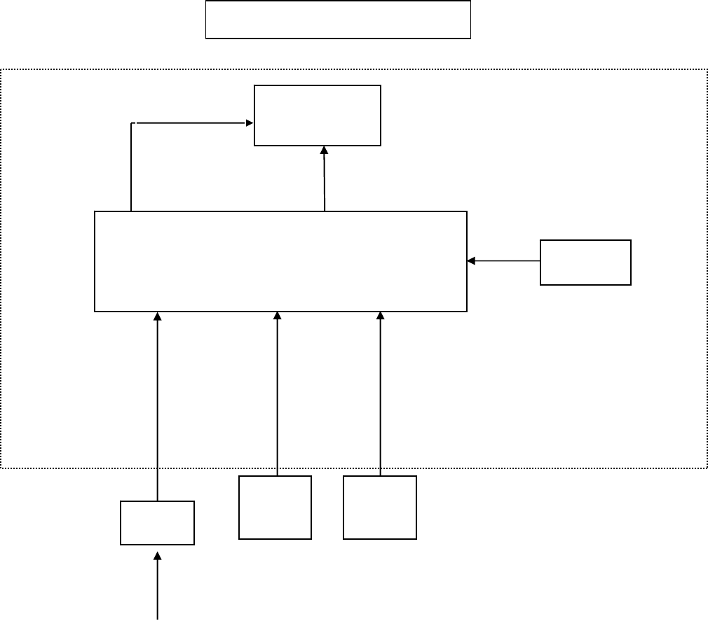
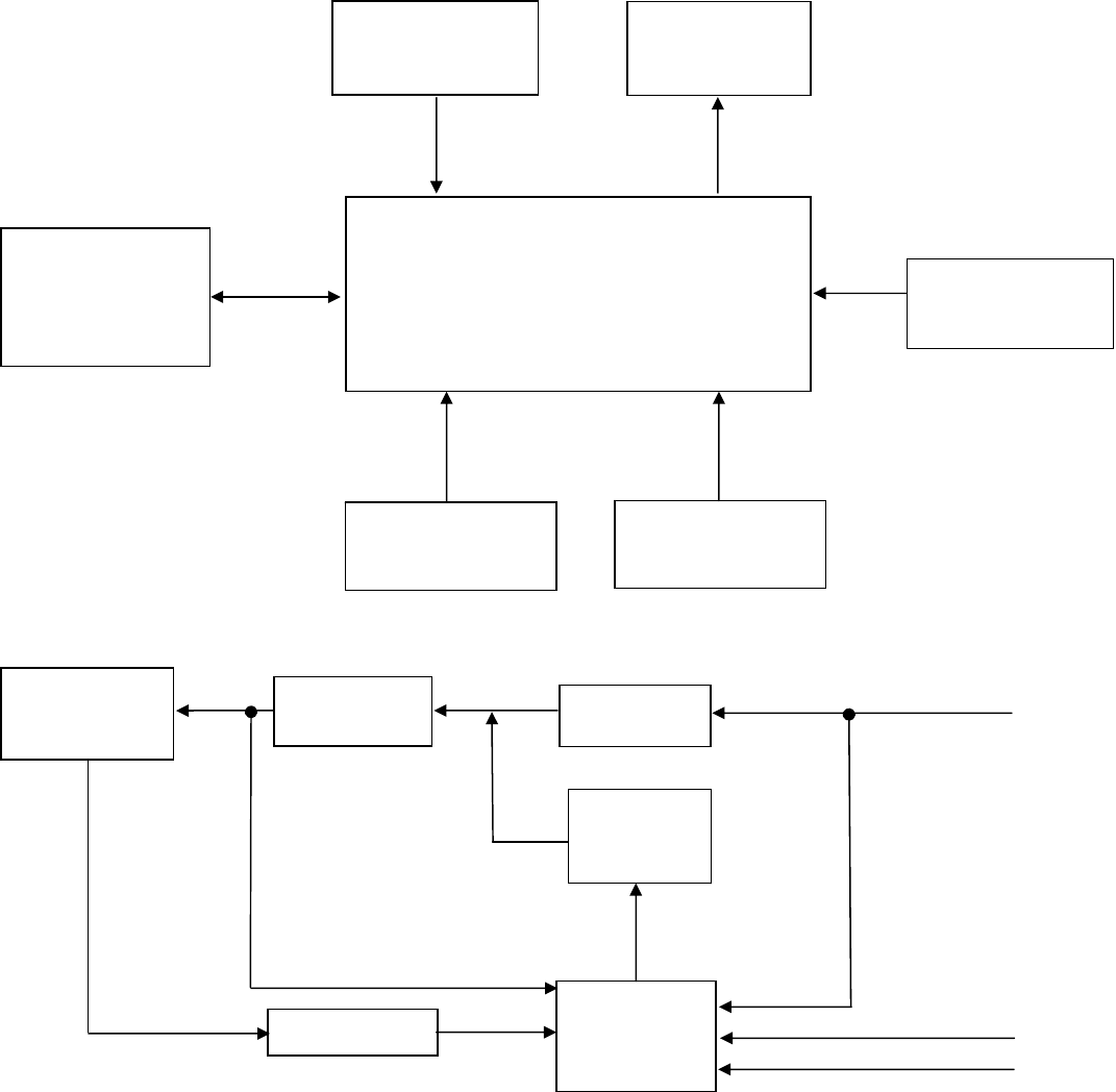
2. LCD Monitor Description
The LCD MONITOR will contain a main board and a key board which house the flat panel control logic, brightness
control logic and DDC.
Monitor Block Diagram
Flat Panel and
LED backlight
Main Board
Key Board
Adapter
D-SUB
Signal
AC-IN
100V~240V
LED Drive.
DVI
Signal

6
3. Operating Instructions
3.1 General Instructions
Press the power button to turn the monitor on or off. The other control knobs are located at front panel of the monitor.
By changing these settings, the picture can be adjusted to your personal preferences.
3.2 Hotkeys
Power
Press the Power button to turn on/off the monitor.
Menu/Enter
Press to display the OSD or confirm the selection
Eco (DCR)/-
Press the Eco key continuously to select the Eco mode of brightness and DCR on when there is no OSD. (Eco mode hot key may
not be available in all models).
4:3 or Wide/+
When there is no OSD, press > continuously to change 4:3 or wide image ratio. (If the product screen size is 4:3 or input signal
resolution is wide format, the hot key is disabled to adjust.)
Source/Auto / Exit
Auto / Exit
When the OSD is closed, press Auto/Source/Exit button continuously about 2 second to do auto configure (only for the models
with dual or more inputs).
When the OSD is closed, press Auto/Source/Exit button will be Source hot key function (Only for the models with dual or more
inputs).
7
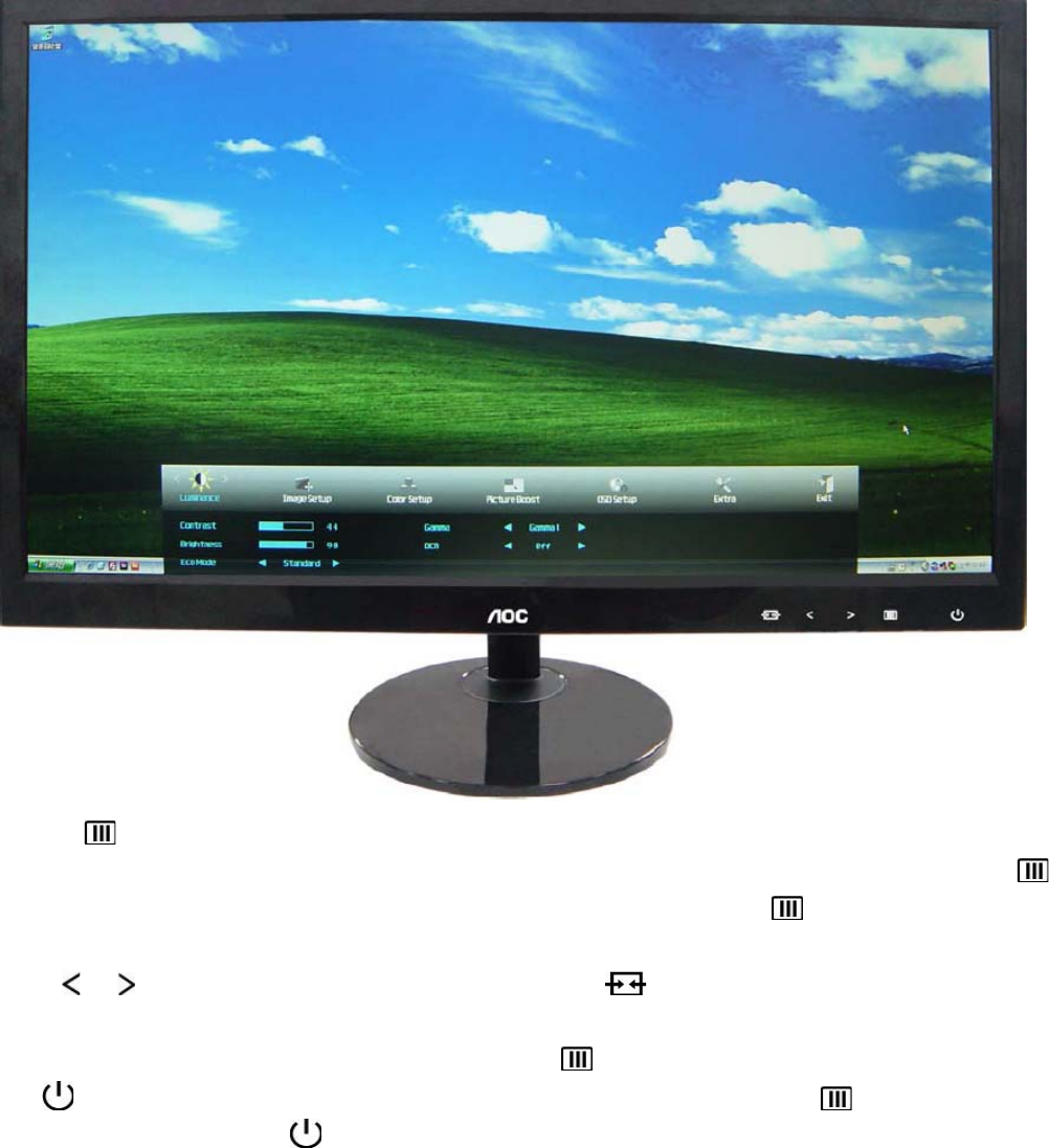
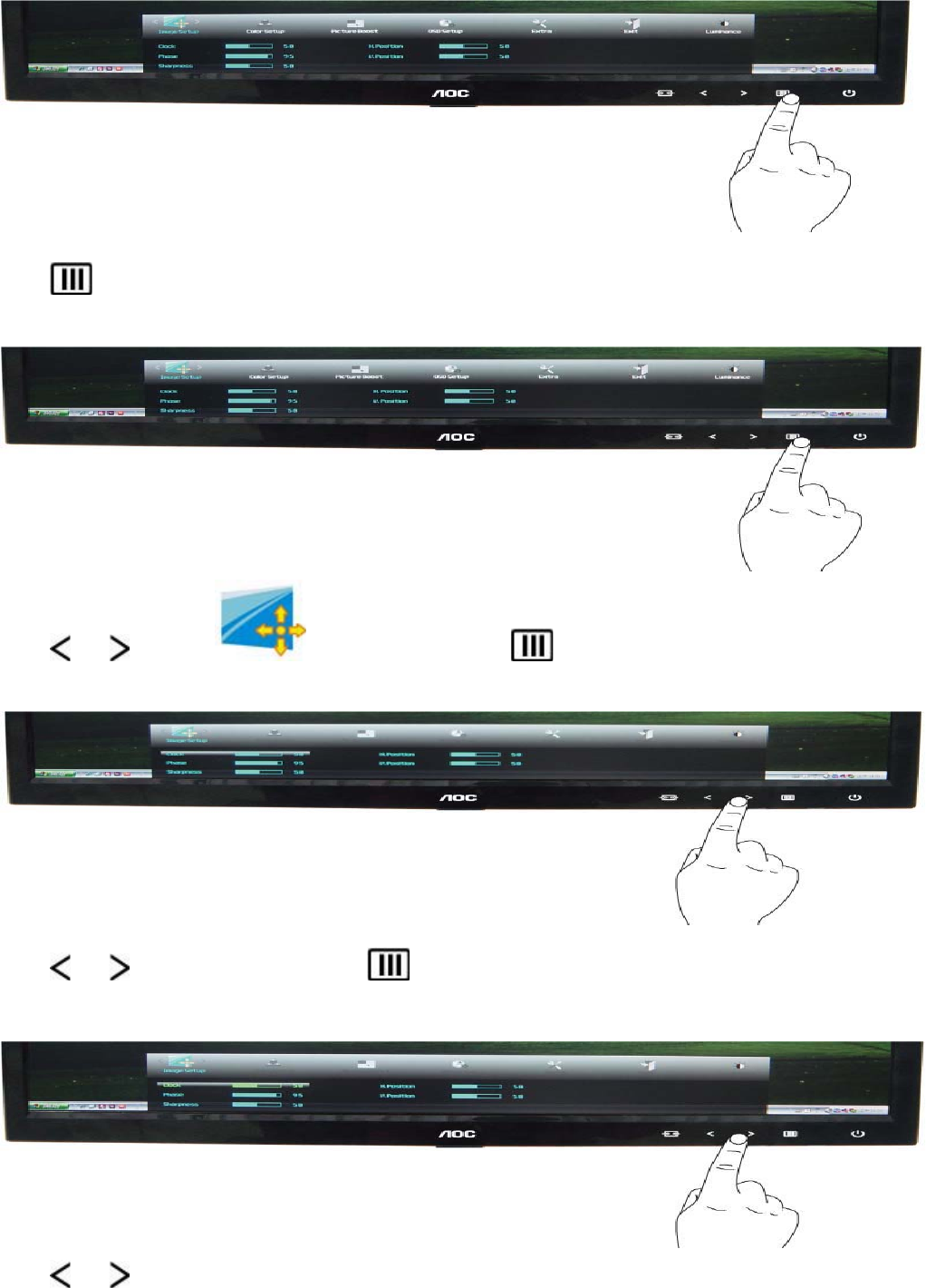
3.3 OSD Setting
Basic and simple instruction on the control keys.
1) Press the MENU-button to activate the OSD window.
2) Press < or > to navigate through the functions. Once the desired function is highlighted, press the
MENU-button to activate sub-menu . Once the desired function is highlighted, press MENU-button to activate
it.
3) Press or to change the settings of the selected function. Press AUTO to exit. If you want to
adjust any other function, repeat steps 2-3.
4) OSD Lock Function: To lock the OSD, press and hold the MENU button while the monitor is off and then
press power button to turn the monitor on. To un-lock the OSD - press and hold the MENU button while
the monitor is off and then press power button to turn the monitor on.
Notes:
1) If the product has only one signal input, the item of "Input Select" is disable to adjust.
2) If the product screen size is 4:3 or input signal resolution is wide format, the item of "Image Ratio" is disable to
adjust.
3) One of DCR, Color Boost, and Picture Boost functions is active, the other two function is turned off accordingly.
8
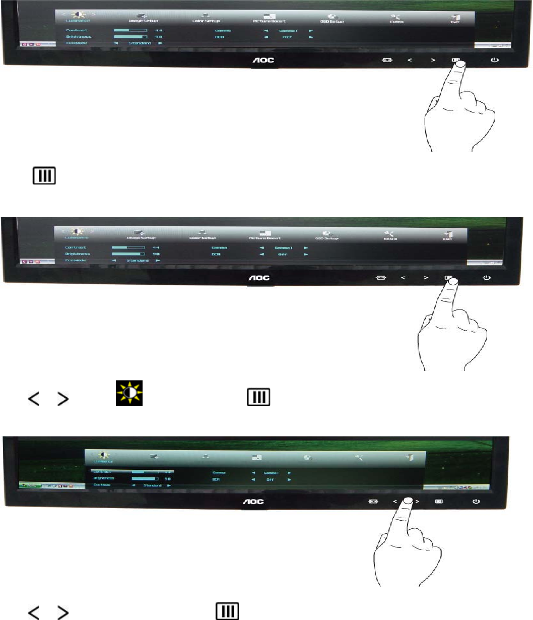
Luminance
1
Press (Menu) to display menu
2
Press or to select (Luminance), and press to enter
3
Press or to select submenu, and press to enter.
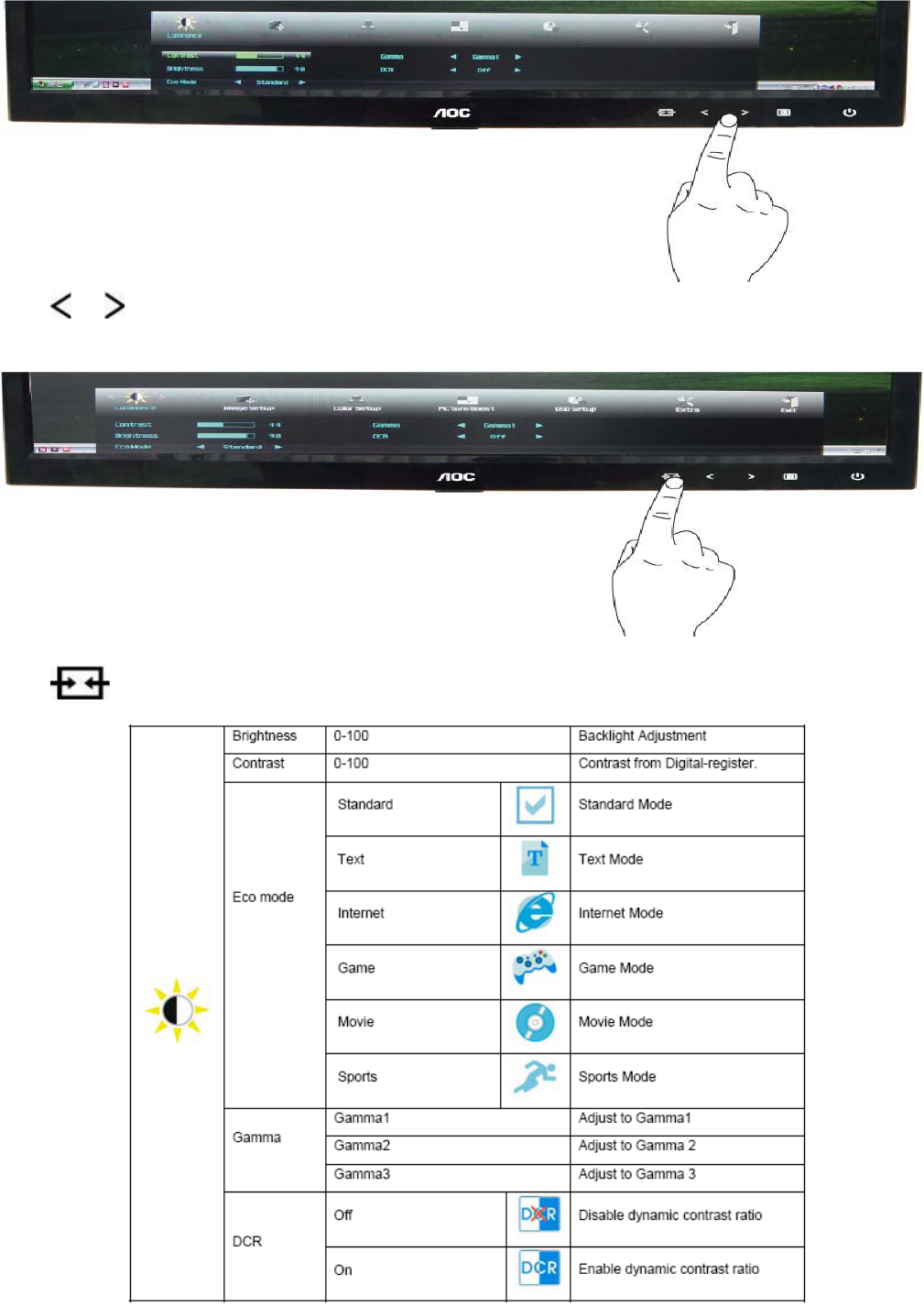
9
4
Press or to adjust
5
Press to exit.
10
Image Setup
1
Press (Menu) to display menu
2
Press or to select (Image Setup) , and press to enter.
3
Press or to select submenu, and press to enter.
4
Press or to adjust.
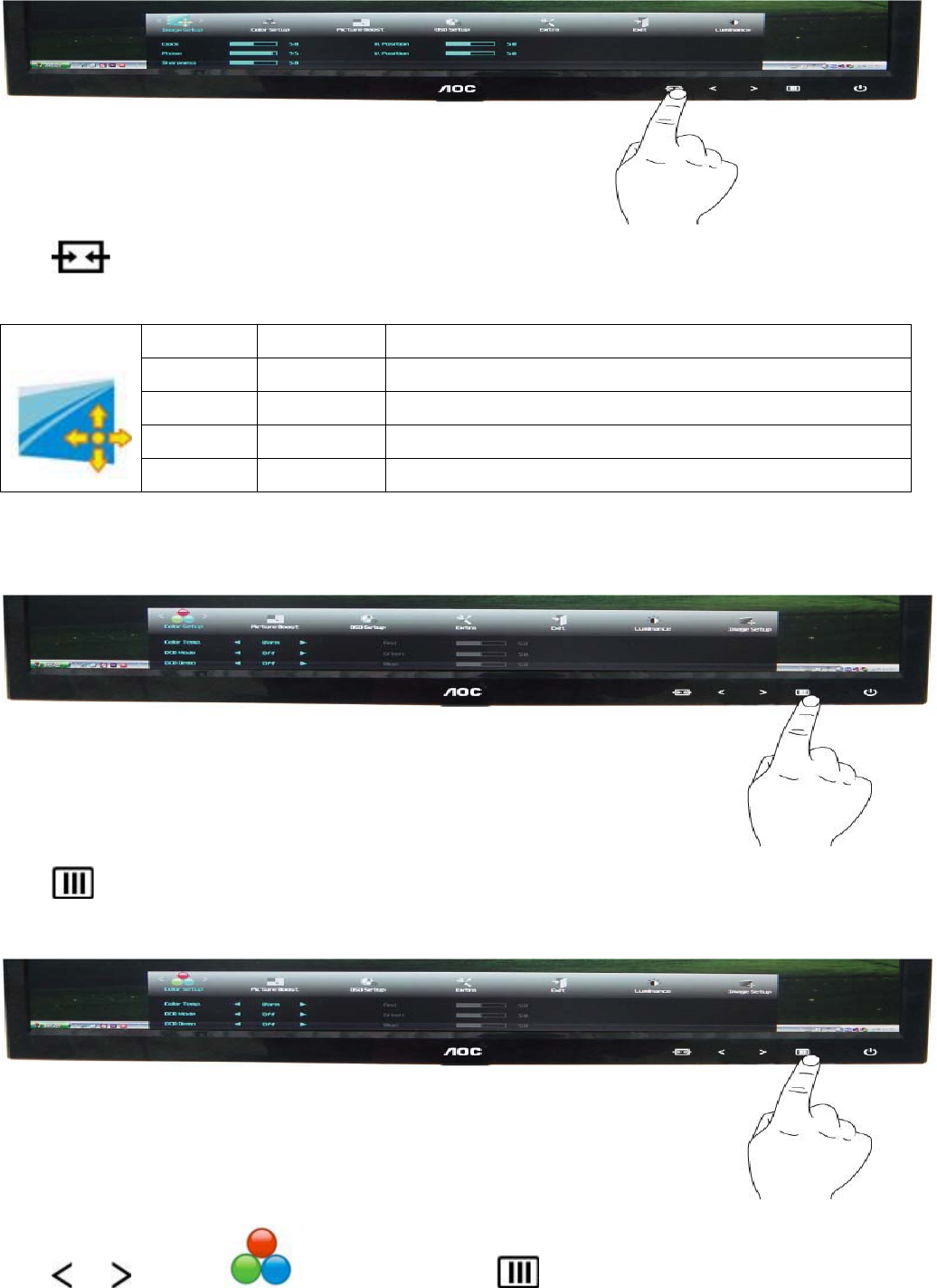
11
5
Press to exit.
Clock 0-100 Adjust picture Clock to reduce Vertical-Line noise.
Phase 0-100 Adjust Picture Phase to reduce Horizontal-Line noise
Sharpness 0-100 Adjust picture sharpness
H.Position 0-100 Adjust the horizontal position of the picture.
V.Position 0-100 Adjust the vertical position of the picture.
Color Setup
1
Press (Menu) to display menu.
2
Press or to select (Color Setup), and press to enter.
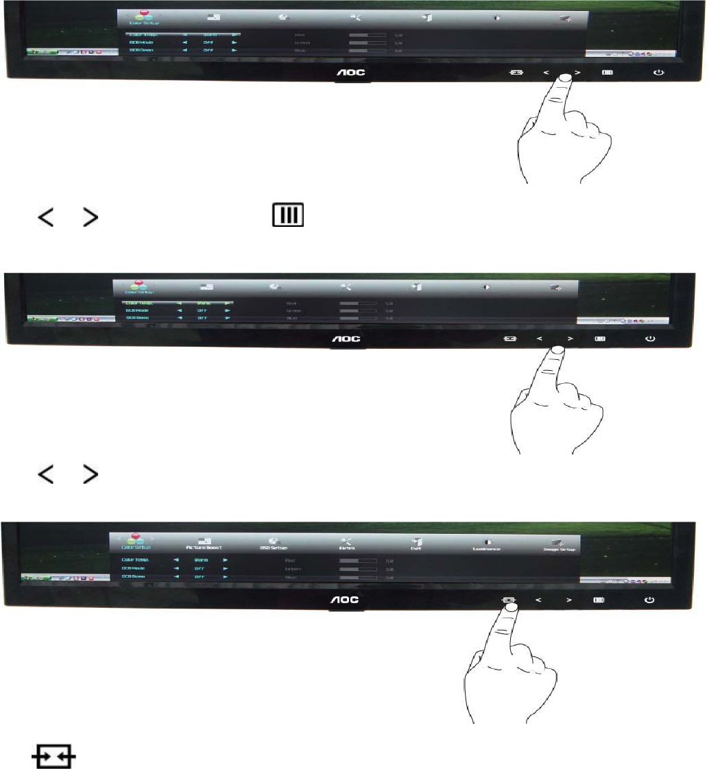
12
3
Press or to select submenu, and press to enter.
4
Press or to adjust.
5
Press to exit.
13
Color setup.
Warm Recall Warm Color Temperature from EEPROM.
Normal Recall Normal Color Temperature from EEPROM.
Cool Recall Cool Color Temperature from EEPROM.
sRGB Recall SRGB Color Temperature from EEPROM.
User
Red Red Gain from Digital-register
Green Green Gain Digital-register.
Blue Blue Gain from Digital-register
DCB Mode
Full
Enhance on or off Disable or Enable Full Enhance Mode
Nature Skin on or off Disable or Enable Nature Skin Mode
Green Field on or off Disable or Enable Green Field Mode
Sky-blue on or off Disable or Enable Sky-blue Mode
AutoDetect on or off Disable or Enable AutoDetect Mode
DCB Demo on or off Disable or Enable Demo
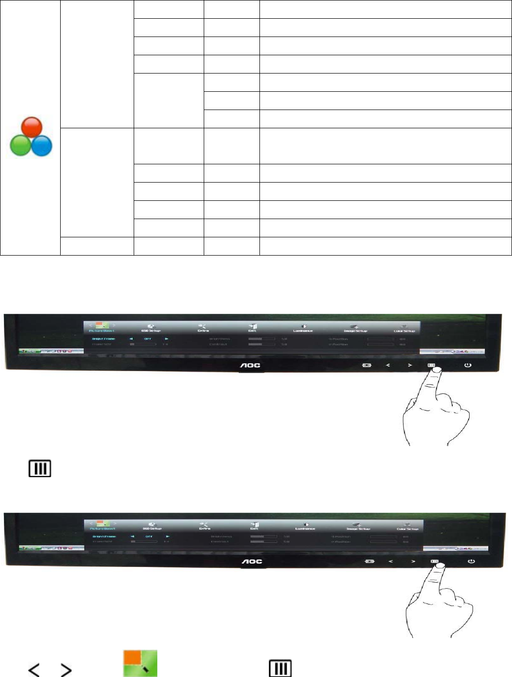
Picture Boost
1
Press (Menu) to display menu.
2
Press or to select (Picture Boost), and press to enter.
3
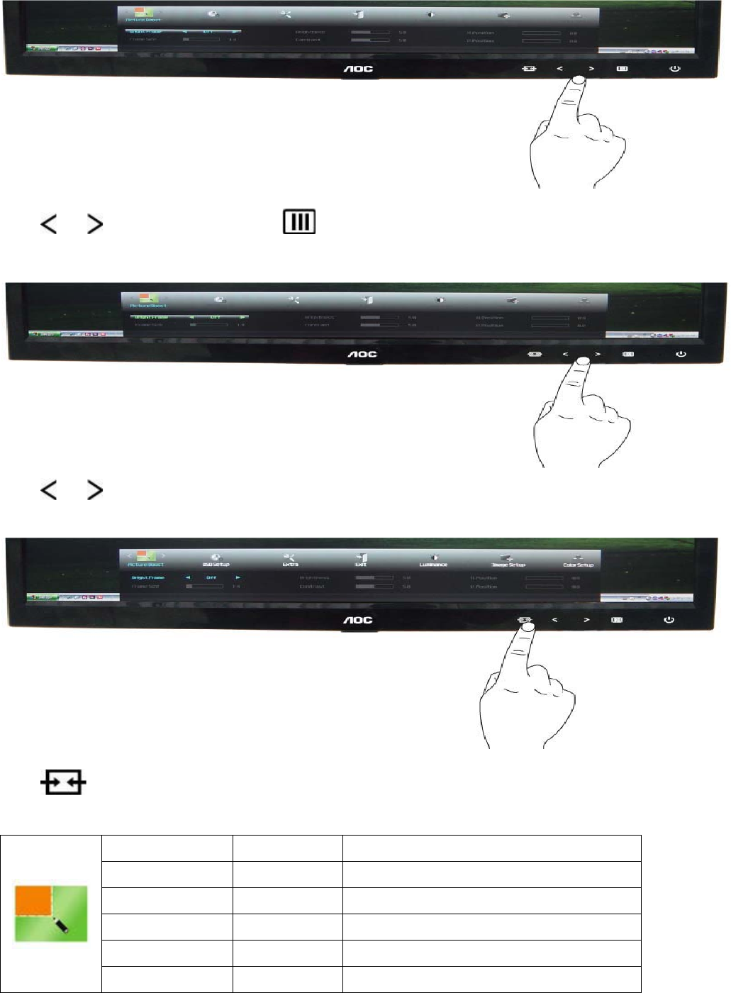
14
Press or to select submenu, and press to enter.
4
Press or to adjust.
5
Press to exit.
Frame Size 14-100 Adjust Frame Size
Brightness 0-100 Adjust Frame Brightness
Contras 0-100 Adjust Frame Contrast
H. position 0-100 Adjust Frame horizontal Position
V.position 0-100 Adjust Frame vertical Position
Bright Frame on or off Disable or Enable Bright Frame
15
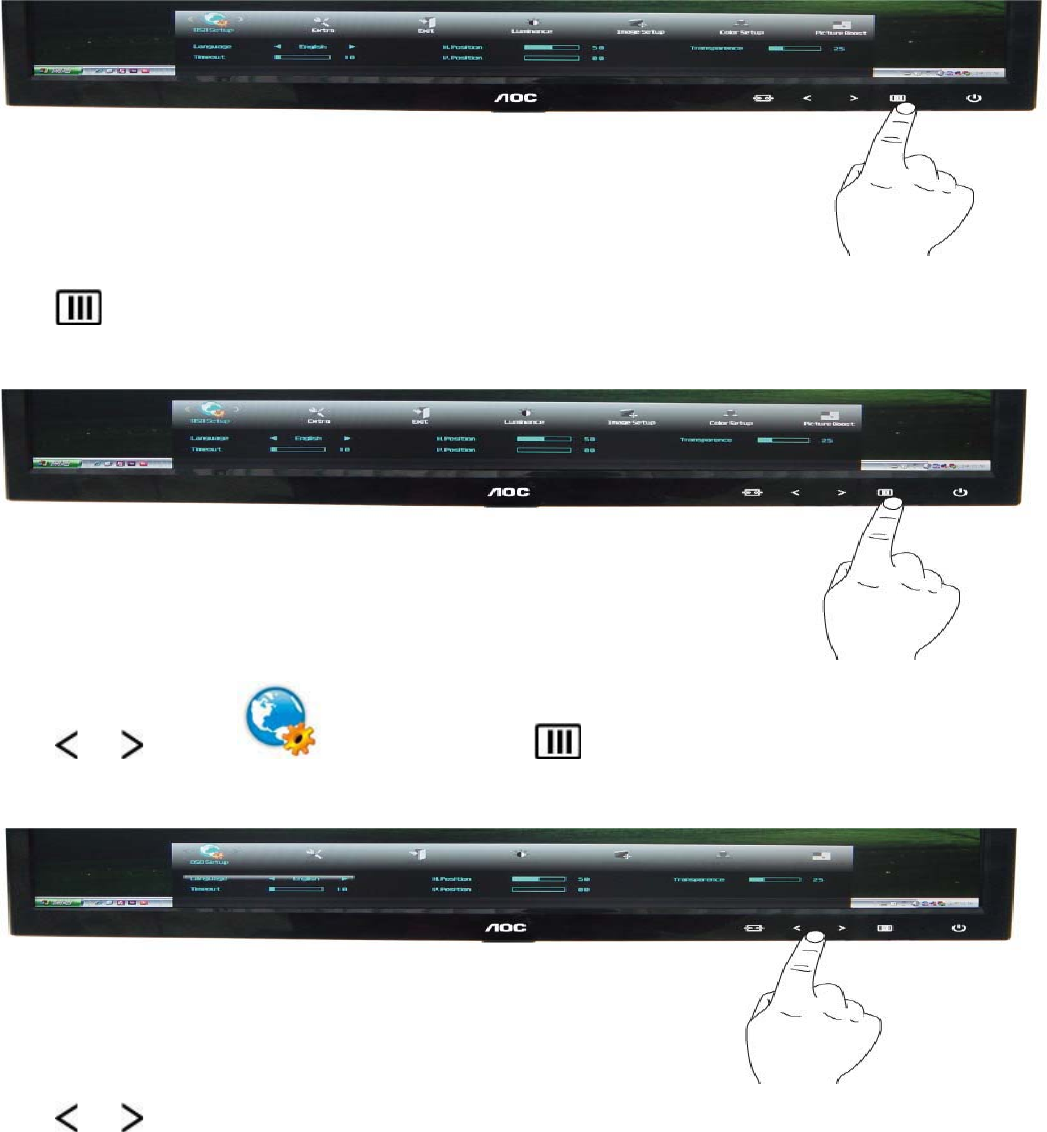
OSD Setup
1
Press (Menu) to display menu.
2
Press or to select (OSD Setup), and press to enter.
3
Press or to select submenu, and press to enter.
16
4
Press or to adjust.
5
Press to exit.
H.Position 0-100 Adjust the horizontal position of OSD
V.Position 0-100 Adjust the vertical position of OSD
Timeout 5-120 Adjust the OSD Timeout
Transparence 0-100 Adjust the transparence of OSD
Language Select the OSD language
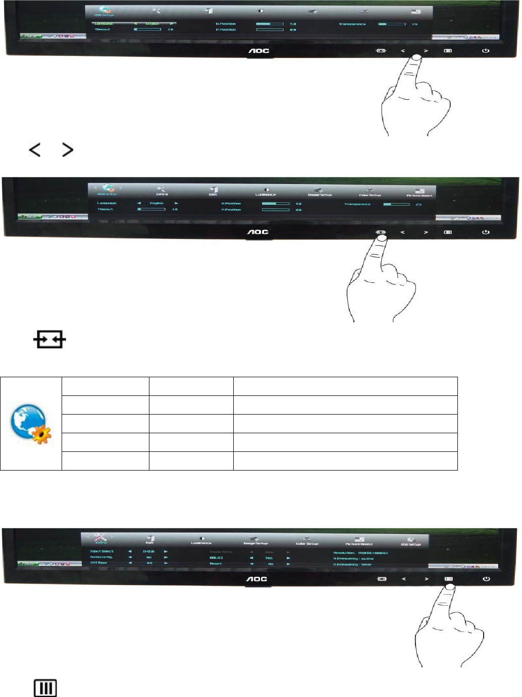
Extra
1
Press (Menu) to display menu.
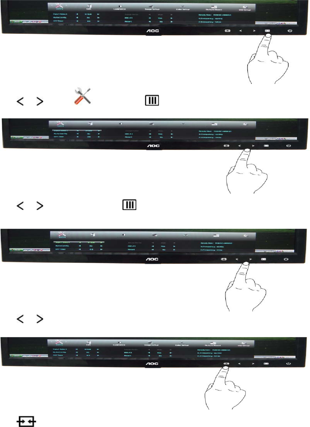
17
2
Press or to select (Extra), and press to enter.
3
Press or to select submenu, and press to enter.
4
Press or to adjust.
5
Press to exit.

18
Exit
1
Press (Menu) to display menu.
2
Press or to select (Exit), and press to exit.
Exit Exit the main OSD
19
20
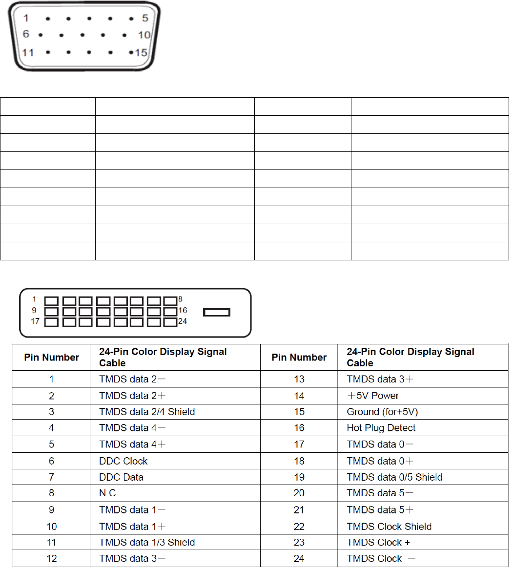
4. Input/Output Specification
4.1 D-SUB CONNECTORS
Pin Assignments
Pin Number 15-Pin Side of the Signal Cable Pin Number 15-Pin Side of the Signal Cable
1 Video-Red 9 +5V
2 Video-Green 10 Ground
3 Video-Blue 11 N.C.
4 N.C. 12 DDC- Serial data
5 Detect Cable 13 H-
sync
6 GND-R 14 V- sync
7 GND-G 15 DDC- Serial clock
8 GND-B

21
4.2 Factory Preset Display Modes

22
4.3 Panel Specification
4.3.1 General Features
BM215WF4-T2BB is a Color Active Matrix Liquid Crystal Display with an integral Light Emitting Diode (LED)
backlight system. The matrix employs a-Si Thin Film Transistor as the active element. It is a transmissive type
display operating in the normally white mode. It has a 21.5 inch diagonally measured active display area with Full
HD resolution (1080 vertical by 1920 horizontal pixel array) Each pixel is divided into Red, Green and Blue
sub-pixels or dots which are arranged in vertical stripes. Gray scale or the brightness of the sub-pixel color is
determined with a 8-bit gray scale signal for each dot, thus, presenting a palette of more than 16,7M colors with
Advanced-FRC(Frame Rate Control). It has been designed to apply the interface method that enables low power,
high speed, low EMI. FPD Link or compatible must be used as a LVDS(Low Voltage Differential Signaling) chip. It is
intended to support applications where thin thickness, wide viewing angle, low power are critical factors and graphic
displays are important. In combination with the vertical arrangement of the sub-pixels, the BM215WF4-T2BB
characteristics provide an excellent flat panel display for office automation products such as monitors.
4.3.2 Display Characteristics
23
4.3.3 Electrical Characteristics
Ta = 25°C
Parameter Symbol Values Unit Notes
Min Typ Max
MODULE :
Power Supply Input Voltage VLCD 4.5 5.0 5.5 Vdc
Permissive Power Input Ripple VLCD - - 0.3 V 3
Power Supply Input Current
ILCD-MOSAIC(60Hz) - 1000 1300 mA 1,5
ILCD-BLACK(60Hz) - 1300 1690 mA 2,5
ILCD-BLACK(75Hz) - 2000 mA 5
Power Consumption PLCD - 5.00 6.5 Watt 1
Inrush current IRUSH - - 3.0 A 1, 4
LED bar Electrical characteristics
Parameter Symbol Condition Values Unit Notes
Min. Typ. Max.
LED : 1,7
LED String Current Is - 110 120 mA 2,7
LED String Voltage Vs 48.0 51.2 54.4 V 3,7
Power Consumption PBar - 11.3 12.0 Watt 4,6,7
LED Life Time LED_LT 30,000 - - Hrs 5,7

24
4.3.4 Optical Characteristics
(Ta=25 °C, VLCD=5.0V, fV=60Hz, DCLK=72MHz, Is=110mA)
Parameter Symbol Values Units Notes
Min Typ Max
Contrast Ratio CR 400 600 -
1
(PR-880)
Surface Luminance, white LWH 160 200 - cd/m2 2
(PR-880)
Luminance Variation WHITE 9P 75 - - %
3
(PR-880)
Response Time Rise Time TrR - 1.3 2.6 ms
4
(RD80S)
Decay Time TrD - 3.7 7.4 ms
Color Coordinates
[CIE1931]
RED Rx
Typ
-0.03
0.642
Typ
+0.03 (PR-650)
Ry 0.332
GREEN Gx 0.305
Gy 0.625
BLUE Bx 0.150
By 0.068
WHITE Wx 0.313
Wy 0.329
Viewing Angle (CR>5)
5
(PR-880)
x axis, right(=0°) r 45 50
Degree
x axis, left (=180°) l 45 50
y axis, up (=90°) u 20 25
y axis, down (=270°) d 40 45
Viewing Angle (CR>10)
x axis, right(=0°) r 40 45
Degree
x axis, left (=180°) l 40 45
y axis, up (=90°) u 10 15
y axis, down (=270°) d 30 35
Crosstalk
1.5 % 6
(PR880)
25
5. Block Diagram
5.1 Main Board
DIM
ON/OFF
Feedback Circuit
D801 L801
PWM Control
MP3389EF
(U801)
12V
LED
(CN803)
MOSFET
(Q806)
H sync
V sync
RGB
CRYSTAL
14.318MHZ (X401)
Flash Memory
Pm25LD020C
(U403)
Scalar IC RTD2281W-CG
(Include ADC, OSD, MCU)
(U401)
Panel Interface
(CN406)
Key Control Interface
(CN405)
DVI Connector
(CN102)
H sync
V sync
RGB
D-Sub Connector
(CN101)
26
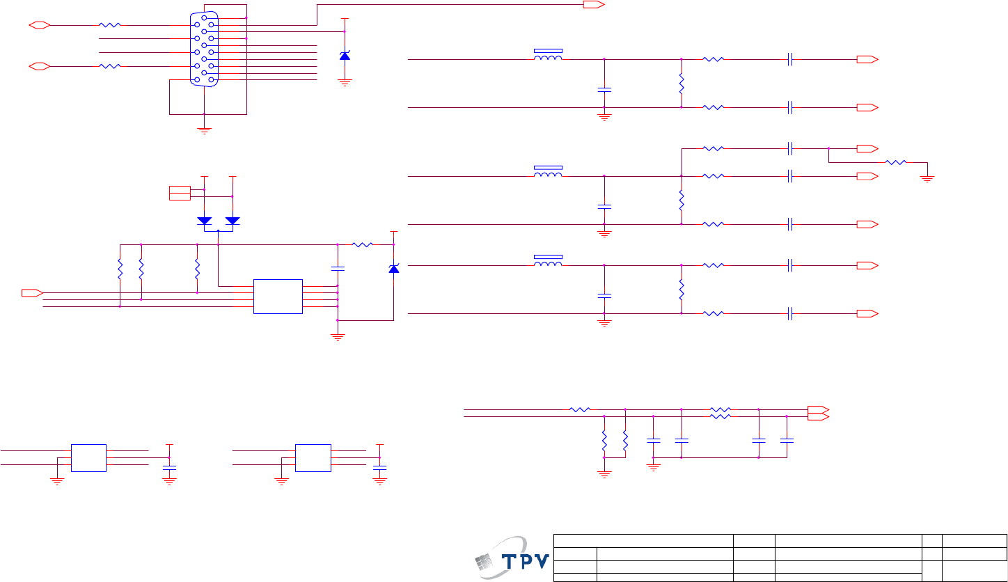
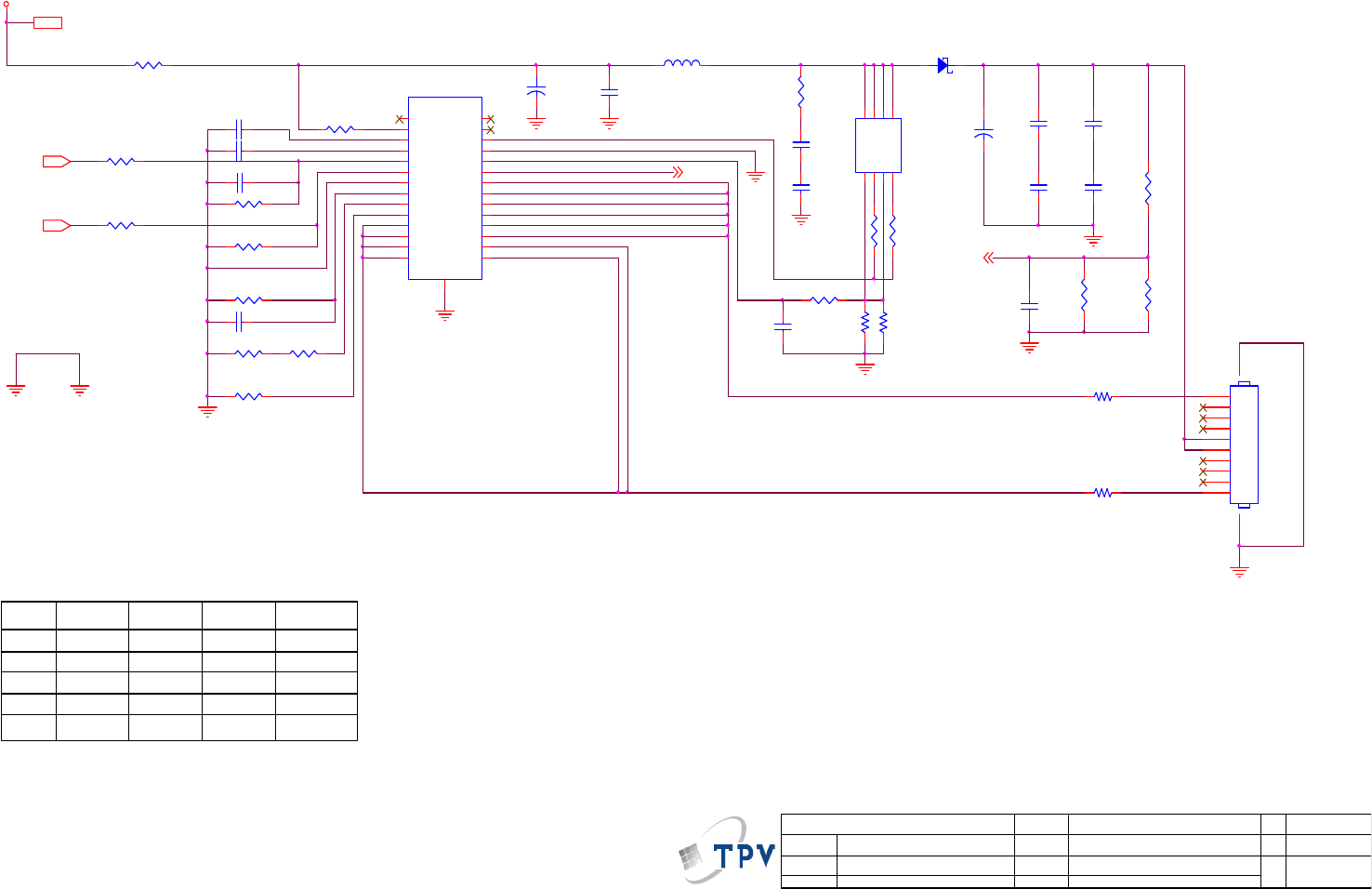
6. Schematic
6.1 Main Board
715G4798M0E000004L
C104
47nF 16V
C105
47nF 16V
BIN0-
RIN0
BIN0
C107
47nF 16V
BIN0
GIN0
RIN0DDCSCL_A
DDCSDA_A
C108
47nF 16V
ESD_VGA
U102
AZC399-04S
I/O1
1
GND
2
I/O2
3I/O3 4
VDD 5
I/O4 6
U101
FM24C02A
A0 1
A1 2
A2 3
GND 4
SDA
5SCL
6WP
7VCC
8
HSIN0
VSIN0
C110
47nF 16V
VGA_5V
+5V
D101
BAV70
3
1
2
C147
22N 25V
R114 22K 1/16W 5%
R113 4K7 1/16W 5%
R112 4K7 1/16W 5%
R101
47R 1/16W 5%
R105
47R 1/16W 5%
U103
AZC399-04S
I/O1
1
GND
2
I/O2
3I/O3 4
VDD 5
I/O4 6
R123
2K2 1/16W 5%
R120 100R 1/16W 5%
EDID_WP4,5
VGA_5V
VGA_5V
AHS0 5
AVS0 5
DET_VGA
B0+ 5
B0- 5
R0- 5
G0+ 5
G0- 5
R0+ 5
GIN0
C112
NC/22pF 50V
ESD_VGA
R121 100R 1/16W 5%
R122
2K2 1/16W 5%
ZD101
RLZ5.6B
1 2
C111
NC/22pF 50V
DDCSDA15RIN0-
GIN0-
BIN0-
SOG 5
R111
47R 1/16W 5%
R109
10R 1/16W 5%
R118
47R 1/16W 5%
R116
10R 1/16W 5%
C145
22pF 50V
C146
22pF 50V
DDCSCL15
ESD_VGA
+5V4,5,7
R150
1K 1/16W 5%
ZD106
RLZ5.6B
1 2
CN101 D-SUB 15P
1
6
2
7
3
8
4
9
5
11
12
13
14
15 10
17 16
BIN0
C113
100N16V
GIN0-
GIN0
RIN0
RIN0-
C114
100N16V
FB105
BEAD
1 2
FB106
BEAD
1 2
R106
75 OHM +-5% 1/16W
R142
1K 1/16W 5%
C103
5PF 50V
R110
75 OHM +-5% 1/16W
DDCSDA_A
C106
5PF 50V
DDCSCL_A
R107
47R 1/16W 5%
R104
10R 1/16W 5%
R119 0R05 1/10W
VSIN0
DET_VGA
DDCSDA1
HSIN0
R117
75 OHM +-5% 1/16W
VGA_5V
DDCSCL1
VSIN0
HSIN0
FB104
BEAD
1 2
C109
5PF 50V
C101
220N16V
R0-
G0+
R0+
B0+
G0-
B0-
DDCSCL1
DDCSDA1
VGA_CABLE_DET 5
VGA_CABLE_DET
R143 NC/1M 1/16W 5%
OEM MODEL
Size
Rev
Date
Sheet
of
TPV MODEL
PCB NAME
称爹
T P V ( Top Victory Electronics Co . , Ltd. )
Key Component
絬
隔
瓜
絪
腹
AOC 50ID A
AOC 50ID B
38Thursday , May 12, 2011
715G4798-M0A <
称爹
>
D-SUB I/O
715G4798-M0A-000-0040_101101
C102
47nF 16V
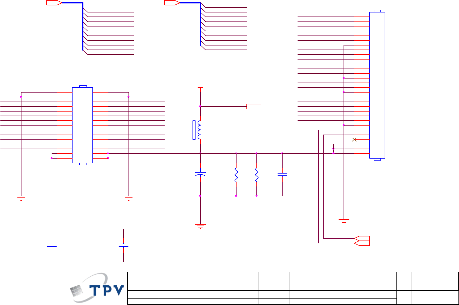
27
RXEC-
RXOC+
RXOC-
C142
100N16V
LVB1PPB6 LVB2MPB5
LVB1MPB7
LVB3PPB0 LVB3MPB1 LVBCKPPB2
FB102
120 OHM
1 2
LVBCKMPB3 LVB2PPB4
PB[0..9]
R147300 OHM 1/4W
LVB0PPB8 LVB0MPB9
RXO0- RXO0+
RXO1- RXO1+
R146300 OHM 1/4W
RXO2-
PA6 LVA1P
RXO2+
PA5 LVA2M
PA0 LVA3P
PA4 LVA2P
PA3 LVACKM
PA1 LVA3M
PA7 LVA1M
PA[0..9]
RXOC-
PA8 LVA0P
RXOC+
RXO3- RXO3+
RXE0-
PB[0..9]5PA[0..9]5
RXE0+
VLCD 7
VLCD
RXE1- RXE1+
RXE2- RXE2+
RXEC- RXEC+
RXE3- RXE3+
+
C141
100UF 16V
RXEC+
L/T_SDA 5
CN407
NC/CONN
2
4
6
8
10
12
14
16
18
20
22
24
26
28
30
1
3
5
7
9
11
13
15
17
19
21
23
25
27
29
PA9 LVA0M
LVA0P RXE0+
PA2 LVACKP
L/T_SCL 5
L/T_SCL
L/T_SDA
LVB2M RXO2-
LVACKM RXEC-
RXE1-LVA1M
RXE2-LVA2M
RXO1-LVB1M
RXO3-LVB3M
RXE3-LVA3M
RXO0-LVB0M
RXE0-LVA0M
RXOC+LVBCKP
LVBCKM RXOC-
RXE2+LVA2P
RXO0+LVB0P
RXO1+LVB1P
RXO3+LVB3P
RXO2+LVB2P
RXEC+LVACKP
RXE1+LVA1P
RXE3+LVA3P
L/T_SCLL/T_SDA
OEM MODEL
Size
Rev
Date
Sheet
of
TPV MODEL
PCB NAME
称爹
T P V ( Top Victory Electronics Co . , Ltd. )
Key Component
絬
隔
瓜
絪
腹
AOC 50ID A
AOC 50ID A
68Thursday , May 12, 2011
715G4798-M0A <
称爹
>
LVDS PANEL I/O
715G4798-M0A-000-0040_101101
C143
NC
CN406
CONN
1
2
3
4
5
6
7
8
9
10
11
12
13
14
15
16
17
18
19
20
21
22
23
24
25
26
27
28
29
30
C144
NC
28
R714
10K +-1% 1/10W
R715
53.6KOHM +-1% 1/10W
C714
100pF 50V
R713
10R 1/10W 5%
C731
22pF 50V
R726
30Kohm 1/16W +/-5%
C722
2N2 50V
R705
4K7 1/16W 5%
C728
1uF 25V
R712
100K 1/16W 5%
+5V 3,4,5
BKLT_EN8
FB702
120 OHM
1 2
BKLT_VBR18
+12V 8
C713
1uF 25V
Q701
LMBT3904LT1G
+
C718
180uF 16V
L701 22UH
C721
100N16V
Adj_BACKLIGHT 5
on_BACKLIGHT 5
D701
SR34
1 2
R711
33K 1/16W 5%
+
C716
470uF 10V
C720
10uF 25V
VCC3.3
C710
100PF
C725
100N16V
+
C707
100UF 16V
U701
VI
3VO 2
GND
1
ZD703 PTZ9.1B
12
Dropout voltage must
< 0.8V @ 600mA
Q706
LMBT3904LT1G
2010/1/25
Q705
AO3401A
2010/2/25
C712
100N 50V
R721
100K 1/16W 5%
C719
100N 50V
R722
NC
Q704
NC/AO4449 -7A/-30V
S
1S
2S
3G
4
D8
D7
D6
D5
R718
4K7 1/16W 5%
R719
10K 1/16W 5%
R720 22K
VLCD 6
Panel_ON5
VLCD
+5V
+5V
+5V
SOT 223
C717
100N16V
+5V
+5V
+5V
+5V
+12V
BKLT_EN
BKLT_VBR1
FB701
BEAD
1 2
C723
10uF 25V
R702
10K 1/16W 5% R703
10K 1/16W 5%
C708
100N16V
C702
NC/100N16V
R704 22K 1/16W 5%
C709
100N16V
R706
100R 1/16W 5%
CN701
JACK
3
2
1
U703
VIN
3VOUT 2
GND
1
U702
G1117-33T43UF
ADJ(GND)
1VOUT(TAB)
2VIN
3
ZD702
NC/RLZ6.2B
1 2
OEM MOD EL
Size
Rev
Date
Sheet
of
TPV MODEL
PCB NAME
称爹
T P V ( Top Victory Electronics Co . , Ltd. )
Key Component
絬
隔
瓜
絪
腹
AOC 50ID D
AOC 50ID C
78Friday , May 13, 2011 <
称爹
>
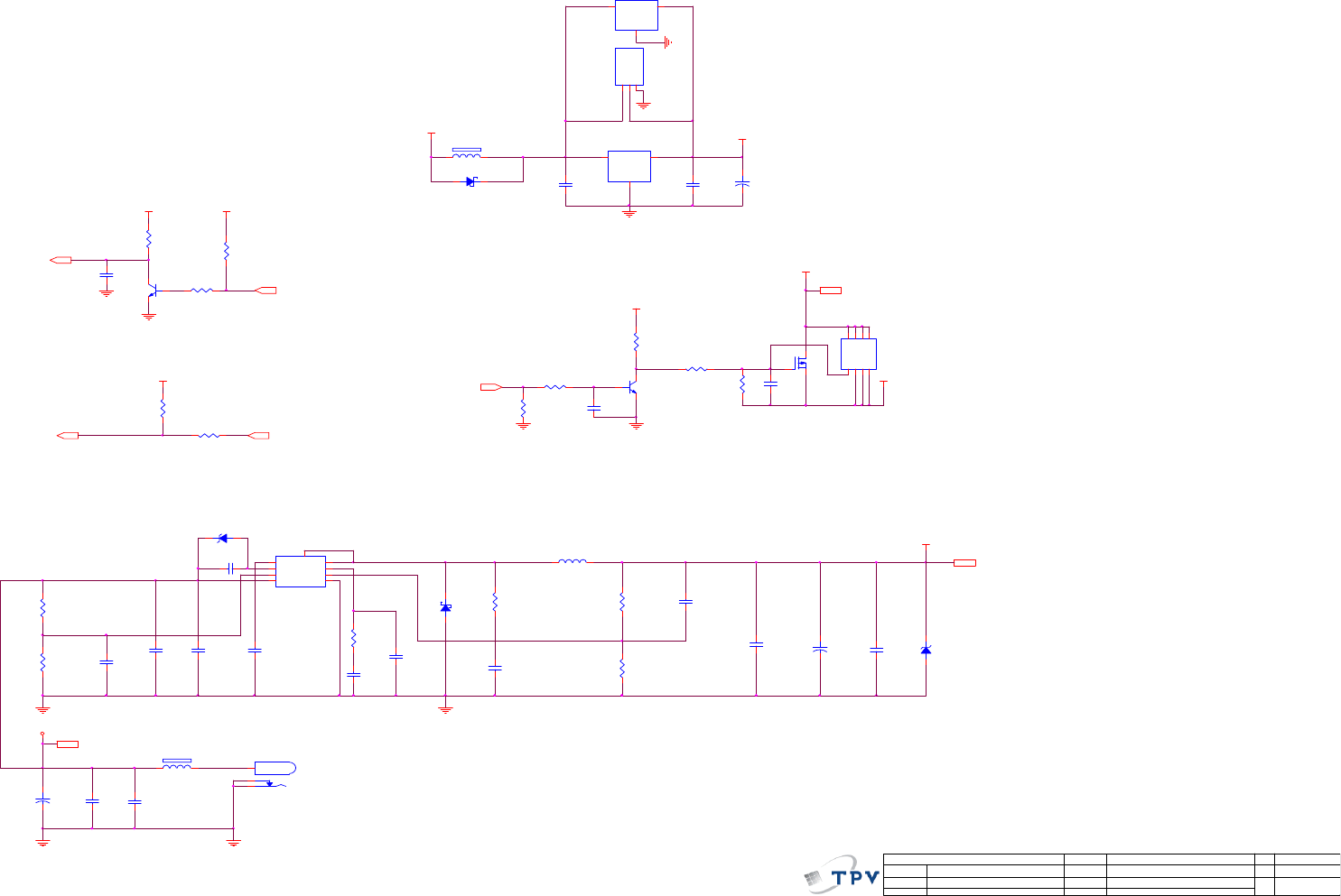
POWER
715G4798-M0A-000-0040_101101
D702
NC/SR34
1 2
U705
APW7080KAITRL
VIN
1EN
2UGND
3VCC
4LX 5
COMP 6
FB 7
GND 8
LX 9
C724
220N16V
C715
1N 50V
29
on_BACKLIGHT7
C401
NC/0.22UF 16V
CN405
CONN
1
2
3
4
5
6
CN403
NC/CONN
1
2
3
4
5
6
7
CN401
NC/CONN
1
2
3
4
5
6
7
8
R440 NC
R441 NC
KEY2
KEY1
EESDA
EESCL
SYSTEM_EEPROM_WP
R404 NC/22K 1/16W 5%
R402 NC/4K7 1/16W 5%
C405 100P 50V
R403 NC/4K7 1/16W 5%
R406
NC/100R 1/16W 5%
R407
NC/100R 1/16W 5%
U402
NC/M24C16
A0 1
A1 2
A2 3
GND 4
SDA
5SCL
6WP
7VCC
8
VCC3.3
POWER
LED_G
LED_A
C406 100P 50V
C413
10uF 10V
C415
22pF 50V
U403
Pm25LD020C-SCE
CE# 1
SO 2
WP# 3
GND 4
VDD
8
HOLD#
7
SCK
6
SI
5
FB407
NC/120 OHM
1 2
C411 100N16V
PA[0..9]6
PA6 LVA1P
PA4 LVA2P
PA0 LVA3P
PA5 LVA2M
C408 100N16V
PA8 LVA0P
PA[0..9]
PA1 LVA3M
PA7 LVA1M
LVACKMPA3
PA9 LVA0M
LVACKPPA2
R482 100R 1/16W 5%
C424
10uF 10V
C409
100N16V
Panel_ON 7
C412
220N16V
D404
NC/RLZ5.6B
R467
4K7 1/16W 5%
C414
100N16V
PB[0..9]6
LVB2MPB5 LVB1PPB6
LEDA
LVBCKPPB2
LVB3PPB0 LVB3MPB1
LVB1MPB7
R415 4K7 1/16W 5%
LVB0MPB9 LVB0PPB8
PB[0..9]
LVB2PPB4 LVBCKMPB3
FB401
NC/120 OHM
1 2
C410 100N16V
HPD_CTRL4
RX2-4RX2+4
M24C16 circuit
RX0-4RX0+4RX1-4RX1+4
C418
22pF 50V
RXC-4RXC+4
R483
0R05 1/16W
FB403
120 OHM
1 2
R479 100R 1/16W 5%
POWER
R480 100R 1/16W 5%
R481 100R 1/16W 5% KEY2
KEY1
R436
390K
R437 100K 1/16W 5%
CABLE_DET DVI_CABLE_DET
R438 220K 1/16W 5%
V33P
DVI_CABLE_DET 4
VGA_CABLE_DET 3
VGA_CABLE_DET
C422 100N16V
LEDG R416 10K 1/16W 5%
V33PVCC3.3
V33TMDS
VCC3.37
D403
RLZ5.6B
1 2
R422 100R 1/16W 5%
R0- 3
R0+ 3
B0+ 3
G0- 3
G0+ 3
SOG 3
AVS0 3
AHS0 3
B0- 3
CN402
NC/CONN
1
2
3
4
5
6
LEDG
VCC3.3
LED_G
R445
2K2 1/16W 5%
Q402
LMBT3906LT1G
+5V 3,4,7
R446
200R 1/10W 5%
+5V
R444 0R05 1/16W
R443 NC
R429 22R 1/16W 5%
R433 22R 1/16W 5% SDIN
SDOUT
CE
CLK
R428 10K 1/16W 5%
FLASH_WP
R435
10K 1/16W 5%
R426
NC
VCC3.3
R427 22R 1/16W 5%
R459
4K7 1/16W 5%
C420
1UF 10V
Adj_BACKLIGHT7
R424 0R05 1/16W
FB404
120 OHM
1 2
LEDA
R451
4K7 1/16W 5%
VCC3.3
LED_A
R455
0R05 1/10W
+5V
R450 NC/0R05 1/16W
R448 0R05 1/16W
Q404
LMBT3906LT1G
X401
14.31818MHZ/32PF
12
R439
0R05 1/16W
R442
NC
XO
XI
R452 0R05 1/16W
R453 0R05 1/16W
C419 100N16V
+5V
D402 NC/RLZ5. 6B
VCC3.3
C402 100N16V
R410
NC/3K9 +/-5% 1/16W
R409
NC/3K9 +/-5% 1/16W
TOUCH_POWER
C425
10uF 10V
R408
NC/3K9 +/-5% 1/16W
VCC3.3
C407
NC/100N 16V
LED_A
D401
RLZ5.6B
1 2
FB408120 OHM
L/T_SDA 6
L/T_SCL 6
R484
NC/100K 1/16W 5%
R431 22R 1/16W 5%
R485
NC/200K 1/16W 5%
DET_+5V
R476
4K7 1/16W 5%
DET_+5V
R475
4K7 1/16W 5%
VCC3.3
R460
NC/100R 1/10W 5% R461
NC/100R 1/10W 5%
R478 47R 1/16W 5%
R477 47R 1/16W 5%
SYSTEM_EEPROM_WP
CN404
NC/CONN
1
2
3
4
5
6
7
C421 NC
V12C
SDOUT
CE
CLK
SDIN
XI
XO
RESETB
V33P
FLASH_WP
R420
4K7 1/16W 5%
C417
100N16V
V12ADC
PA0 LVA3P
PA6 LVA1P
PA4 LVA2P
PA5 LVA2M
PA1 LVA3M
LVB0MPB9
PA9 LVA0M
PA8 LVA0P
PA7 LVA1M
LVB2MPB5 LVB1PPB6 LVB1MPB7 LVB0PPB8
LVBCKPPB2 LVBCKMPB3 LVB2PPB4
LVB3PPB0 LVB3MPB1
DDCSCL24
V33P
DDCSDA24R425 0R05 1/16W
LVACKMPA3 LVACKPPA2
CABLE_DET
EESCL
EDID_W P EDID_WP 3,4
EESDA
V33TMDS
R430 6.2KOHM +-1% 1/10W
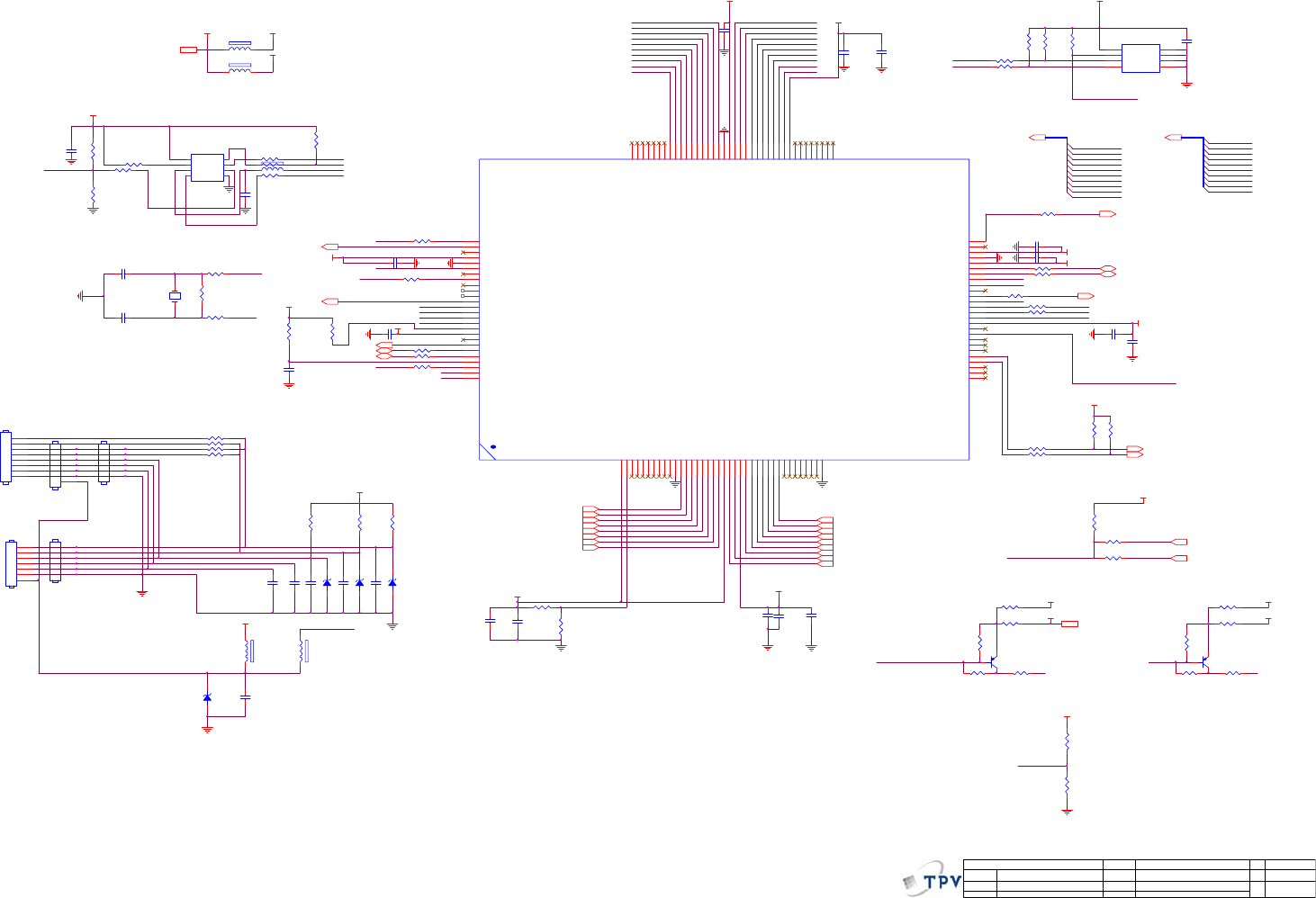
U401
RTD2281W-CG
TMDS_VDD
1
TMDS_REXT
2
NC
3
NC
4
NC
5
NC
6
NC
7
NC
8
NC
9
NC
10
TMDS_GND
11
RX2P_1
12
RX2N_1
13
RX1P_1
14
RX1N_1
15
RX0P_1
16
RX0N_1
17
RXCP_1
18
RXCN_1
19
TMDS_VDD2
20
AVS0
21
AHS0
22
ADC_VDD
23
B0-
24
B0+
25
G0-
26
G0+
27
SOG0
28
R0-
29
R0+
30
GPI
31
GPI
32
ADC_GND
38 GPI
37 GPI
36 GPI
35 GPI
34 GPI
33
GPIO 45
GPIO 44
A-ADC0 / GPIO 50
A-ADC1 / GPIO 51
A-ADC2 / GPIO 52
A-ADC3 / GPIO 53
GPIO 54
TCON[0][5] / PWM1 / PWM5 / GPIO 55
TCON[1][4] / IICSCL / GPIO 56
GPIO/TCON[5] 41
TCON[9][11] / IICSDA / GPIO 57
TCON[7][10] / DDCSCL1 / GPIO 58
TCON[3][5] / DDCSDA1 / GPIO 59
VCCK 60
PGND 61
PVCC 62
TCON[1][8] / PWM2 / GPIO 63
SD0 / SPDIF0 / TCON[0][7] / GPIO / PWM0 64
GPIO 47
PWM0 / GPIO 48
BB3N / SCK / TCON[4][2] / GPI / GPO / BLU7 66
BB2P / MCK / TCON[5][9] / GPI / GPO / BLU6 67
BB2N / SD0 / SPDIF 0 / TCON[13][3] / GPI / GPO / BLU5 68
IICSCL / GPIO 42
BB1P / SPDIF1 / SD1 / TCON[7][3] / GPI / GPO / IICSCL / BLU4 69
BB1N / SPDIF2 / SD2 / TCON[9][11] / GPI / GPO / IICSDA / BLU3 70
BCLKP / SPDIF3 / SD3 / TCON[10][8] / GPI / GPO / PWM1 / PWM5 / BLU2 71
BCLKN / TCON[6][12] / GPI / GPO / PWM3 72
NC 73
BG3P / BLU7 / BLU 1 / GPI / GPO / TXO3+_8b / IIS_SD0 (SPDIF0) 74
BG3N / BLU0 / BLU6 / GPI / GPO / TXO3-_8b / IIS_MCK (SPDIF1) 75
BG2P / GRN7 / GPI / GPO / BLU5 / TXOC+_8b 76
BG2N / GRN6 / GPI / GPO / BLU4 / TXOC-_8b 77
GPIO 46
PVCC 84
PGND 85
BR1P / RED7 / GRN3 / TXE3+_8b 86
IICSDA / GPIO 43
AG2N / GPI / GPO / PWM3 / TCON[11][6] 99
GPI 40
NC 49
AR1P / MCK / TCON[7] / GPI / GPO
108
GPI 39
XO
127
XI
128
BB3P / WS / TCON[7][1] / GPI / GPO / PWM1 65
BG1P / GRN5 / GPI / GPO / BLU3 / TXO2+_8b / IIS_SCK (SPDIF2) 78
BG1N / GRN4 / GPI / GPO / BLU2 / TXO2-_8b / IIS_WS (SPDIF3) 79
BR3P / GRN3 / GPI / GPO / GRN7 / TXO1+_8b 80
BR3N / GRN2 / GPI / GPO / GRN6 / TXO1-_8b 81
BR2P / GRN1 / GPI / GPO / GRN5 / TXO0+_8b 82
BR2N / GRN0 / GPI / GPO / GRN4 / TXO0-_8b 83
BR1N / RED6 / GRN2 / TXE3-_8b 87
AB3P / RED5 / RED7 / TXEC+_8b 88
AB3N / RED4 / RED6 / TXEC-_8b 89
AB2P / RED3 / RED5 / TXE2+_8b 90
AB2N / RED2 / RED4 / TXE2-_8b 91
AB1P / RED1 / RED3 / TXE1+_8b 92
AB1N / RED0 / RED2 / TXE1-_8b 93
ACLKP / DENA / TXE0+_8b 94
ACLKN / DHS / TXE0-_8b 95
AG3P / DCLK / GPI / GPO / PWM0 96
AG3N / DVS / GPI / GPO / PWM1 97
AG2P / GPI / GPO/ PWM2 98
AG1P / GPI / GPO / PWM4 / TCON[12][3] 100
AG1N / GPI / GPO / PWM5 / TCON[0] 101
AR3P / SD3 / SPDIF3 / TCON[10] / GPI / GPO / PWM0 102
AR3N / SD2 / SPDIF2 / TCON[8] / GPI / GPO / IICSCL / PWM1
103
AR2P / SD1 / SPDIF1 / TCON[5] / GPI / GPO / IRQB / IICSDA
104
AR2N / SD0 / SPDIF0 / TCON[9] / GPI / GPO
105
PVCC
106
PGND
107
AR1N / SCK / TCON[3] / GPI / GPO
109
WS(SD1) / TCON[2][6][7] / GPIO
110
SD0 / SPDIF0 / TCON[4][7] / GPIO
111
SD1(WS) / SPDIF1 / TCON[5][9] / GPIO
112
SD2(SCK) / SPDIF2 / TCON[1][11] / GPIO
113
SD3(MCK) / SPDIF3 / TCON[0][13] / PWM4 / GPIO
114
SPI_SCLK / SDIO
115
SI / MCU_SCLK
116
SO / SCSB
117
CEB / IRQB
118
GPO / PWM5
119
VCCK
120
DDCSCL3 / GPIO
121
DDCSDA3 / GPIO
122
DDCSCL2 / GPIO
124 DDCSDA2 / GPIO
123
RESETB
125
GPIO / PWM1
126
R434
NC
OEM MODEL
Size
Rev
Date Sheet of
TPV MOD EL
PCB NAME 称爹
T P V ( Top Victory Electronics Co . , Ltd. )
Key Component
絬
隔
瓜
絪
腹
AOC 50ID A
AOC 50ID Custom
58Thursday , May 12, 2011
715G4798-M0A <
称爹
>
SCALER
715G4798-M0A-000-0040_101101
DDCSCL1 3
DDCSDA1 3
R421 0R05 1/16W
R419 0R05 1/16W
C423
NC/10uF 10V
V12C
V33P
C403 100N16V
V12C
V33P
V33P
C416
1UF 10V
C404 100P 50V
C15122pF 50V
30
R841
2.2OHM 1/10W
R842
2.2OHM 1/10W
R819
33K 1/16W 5%
+
C811
NC/470uF 16V
R809
6.2KOHM +-1% 1/10W
Q806
P8008HV
S1
1
G1
2
S2
3
G2
4
D1 8
D1 7
D2 6
D2 5
R803
33K 1/16W 5%
C801 0.47uF 16V
+12V
2010/6/2
2010/2/9
R816
6.8K
0.15 ohm
BKLT_EN7
0.2 ohm
BKLT_VBR17
NC
+12V 7
190W
R809
0.2 ohm
6.2K
NC
230W
R834
200W
NC
0.12 ohm
215W
6.2K
R812
R805
300K 1/8W 5%
39K
6.2K
NC
C802 68NF 50V
+
C807
4.7UF 100V
R807 20K 1/10W 5%
L801
47UH
R810 20K 1/10W 5%
D801
BR310
1 2
C808 NC
R801
10R 1/8W 5%
R812
0.12R 1%
270K
0.15 ohm
It is suitable for 18.5", 20",21.5'' & 23" LED panel
270K
R806 1K 1/10W 5%
C809
1000pF 50V
R827 1R 1/10W 5%
C805
1000pF 50V
C813
2N2 50V
R804 100K 1/16W 5%
C814
2N2 50V
U801
MP3389EF
NC
1
VIN
2
VCC
3
COMP
4
EN
5
DBRT
6
GND
7
OSC
8
ISET
9
BOSC
10
LED12
11
LED11
12
LED10
13
LED9
14 LED8 15
LED7 16
LED6 17
LED5 18
LED4 19
LED3 20
LED2 21
LED1 22
OVP 23
ISENSE 24
PGND 25
GATE 26
VFAULT 27
NC 28
E-Pad
29
R808 1K 1/10W 5%
R811
150R 1/10W 5%
OEM MODEL
Size
Rev
Date
Sheet
of
TPV MODEL
PCB NAME
称爹
T P V ( Top Victory Electronics Co . , Ltd. )
Key Component
絬
隔
瓜
絪
腹
AOC 50ID C
AOC 50ID Custom
88Thursday , May 12, 2011 <
称爹
>
CONVERT
715G4798-M0A-000-0040_101101
R843
680 OHM 1/4W
CN803
CONN
1
2
3
4
5
6
7
8
9
10
1112
R834
270K +-1% 1/10W
C803
0.47UF 50V
C804
0.47UF 50V
R816
NC
R813
0R05
R830 1R 1/10W 5%
OVP
C806
100pF 50V
C815
100pF 50V
OVP
C812 100N 50V
R802 270K +-1% 1/10W
C810
100N 50V
31
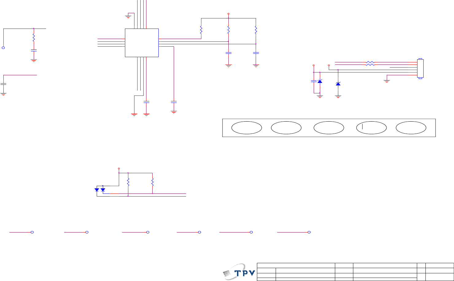
6.2 Key Board
715G4842K0E000004F
5V_LED DATA
SM_CLK
SM_INT#
R006 0R05 1/16W
ZD001
UDZSNP5.6B
1 2
ZD002
UDZSNP5.6B
1 2
CN001
CABLE
1
2
3
4
5
6
R005 0R05 1/16W
CIN_03
CIN_07
CIN_11
5V_LED
CIN_01
+
-
R007
4K7 1/16W 5%
V3.3
R008
4K7 1/16W 5%
OEM MODEL
Size
Rev
Date Sheet of
TPV MODEL
PCB NAME 称爹
T P V ( Top Victory Electronics Co . , Ltd. )
Key Component
絬
隔
瓜
絪
腹
e943Fw C
AOC e943Fw A3
22Tuesday , April 19, 2011
715G4164-K0C <
称爹
>
2.0 Touch key
715G4164-K0C-000-0040_20100420.DSN
R003
4K7 1/16W 5%
R004
100R 1/16W 5%
C004
12P 50V
C008
100P 50V
C007
100nF 25V
CIN_01
Dif f erential KEY0.1524
CIN_05
C005
100nF 25V
Differential
C006
100nF 25V
GPIO_00
SM_CLK
U001
IT7230EFN/BX
CIN03
1
CIN07
2
CIN09
3
CIN11
4
VSHILD
5
VBIAS
6
AVSS
7
AVCC
8
DVCC 9
SCLK 10
SDA 11
INT# 12
GPIO0 13
GPIO1 14
CIN00 15
CIN01 16
E-PAD 17
CIN_09
Auto
CIN_03
-
SM_INT#
SM_DATA
CIN_05
GPIO_01
Power
V3.3
V3.3
Menu+
AC_SHIELD
VBIAS
Auto
Power
R001
10K 1/16W 5%
C003
12P 50V
CIN_11
AC_SHIELD
CIN_07CIN_09
AUTO_4 KEY0.1524 -_2 KEY0.1524
Orange
Blue
D001
2
3
1
MENU_5 KEY0.1524
+_3 KEY0.1524
R002
4K7 1/16W 5%
PWR_1 KEY0.1524
GPIO_01
GPIO_00
TP2
KEY0.1524
VBIAS
MENU
CLK
C011
1UF 10V
V3.3 SM_DATA
32
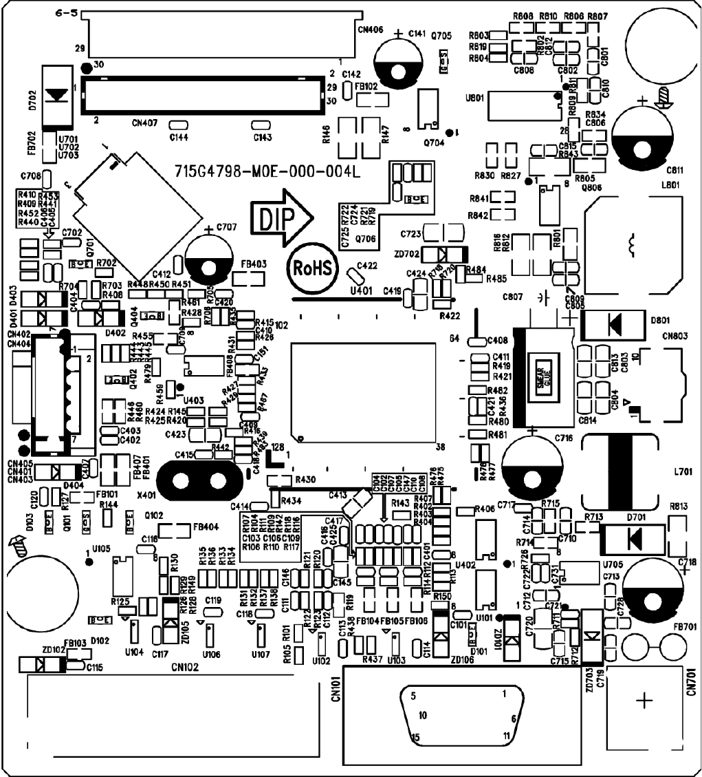
7. PCB Layout
7.1 Main Board
33
34
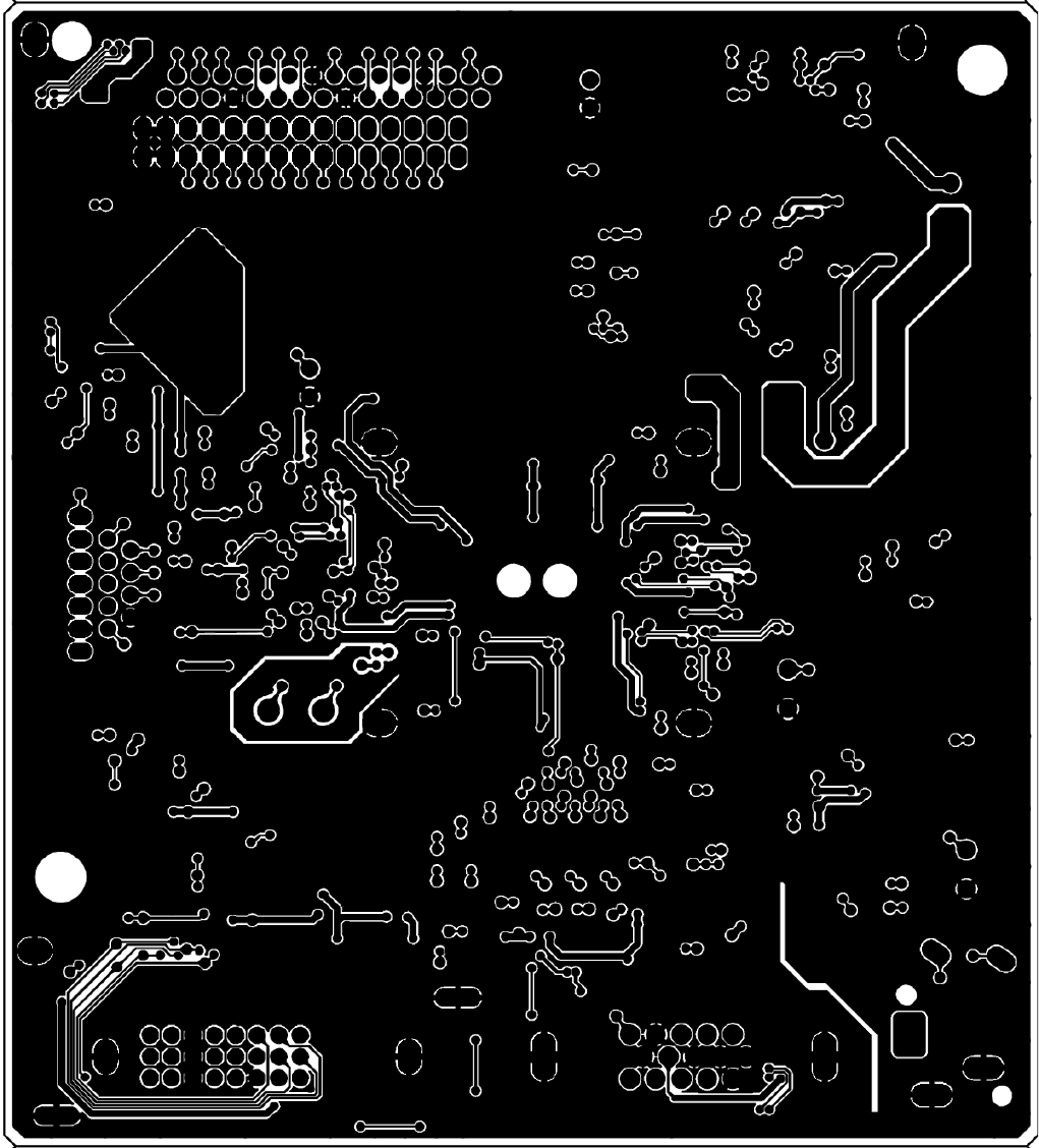
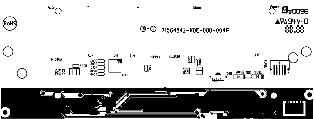
7.2 Key Board
715G4842K0E000004F
35
8. Maintainability
8.1 Equipments and Tools Requirement
1. Voltmeter.
2. Oscilloscope.
3. Pattern Generator.
4. DDC Tool with an IBM Compatible Computer.
5. Alignment Tool.
6. LCD Color Analyzer.
7. Service Manual.
8. User Manual.
36
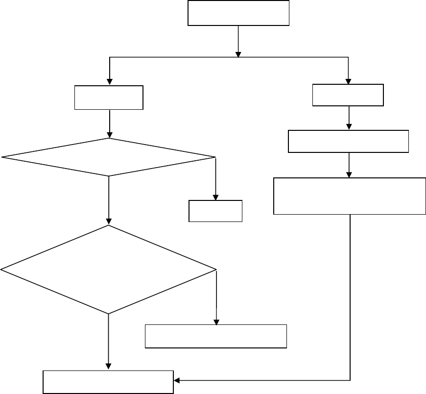
8.2 Trouble Shooting
1. No Power
OK
No power
Check power cable is
tightened?
Check Power “On/Off”
is “On”?
Re-plug the power cable
Replace key board and check connections
Check the LED
indicate is OK? Check the AC power
Replace main board and check connections
OK
NG
OK
NG
Turn on the Power “On/Off” switch
37
2. No Video (Power LED White)
No Video (Power LED White)
Press the power
button is OK?
Check the LVDS/FFC
cable or panel
The end
NG
OK
Replace the main board
Replace the LVDS/FFC
cable or panel
Replace the key board
NG
Replace the main
board and connection
OK
OK
38
3. DIM
OK
The end
OK
The end
OK
The end
DIM (image overlap, focus or flicker)
Reset in factory mode
Set to the optimal
frequency, select the
recommended fre
q
uenc
y
Pull out signal cable and
check “Self Test Feature
Check” is ok?
Check the signal cable
and the PC
Readjust the phase and pixel
clock in the user mode
Replace the main board
Replace the panel
NG
NG
NG
OK
NG
NG
OK The end
OK
NG
39
4. Color is not optimal
NG
Color is not optimal
Miss color Color shift
Replace the signal cable
Pull out the signal cable
and check the screen
color display is normal?
The end
Replace the signal cable or PC
Reset the factory mode
In the user mode, set the” color
settin
g
s” until customer satisf
y
Replace the main board
NG
OK
NG
OK
NG
40
9. White- Balance, Luminance Adjustment
Approximately 30 minutes should be allowed for warm up before proceeding white balance adjustment.
How to setting MEM channel you can reference to chroma 7120 user guide or simpl use “SC” key and “NEXT” Key
to modify xyY value and use “ID” key to modify the TEXT description Following is the procedure to do white-balance
adjust .
2. Setting the color temp. you want
A. MEM.CHANNEL 3 Warm (6500K):
Warm color temp. parameter is x = 313 ±30, y = 329 ±30
B. MEM.CHANNEL 4 Normal (7300K):
Normal color temp. parameter is x = 301 ±30, y = 317 ±30
C. MEM.CHANNEL 9 Cool (9300K):
Cool color temp. parameter is x = 283 ±30, y = 297 ±30
D. MEM.CHANNEL 10 (sRGB color):
sRGB color temp. parameter is x = 313 ±30, y = 329 ±30
3. Enter into the factory mode
Turn off the power, press two direction keys and turn the power on. Then press the “MENU” button. The factory OSD
will appear.
4. Gain adjustment:
Move cursor to “-F-” and press MENU key
A. Adjust Warm (6500K) color-temperature
1. Switch the chroma-7120 to RGB-Mode (with press “MODE” button)
2. Switch the MEM.channel to Channel 3 (with up or down arrow on chroma 7120)
3. The LCD-indicator on chroma 7120 will show x = 313 ±30, y = 329 ±30
4. Adjust the RED on factory window until chroma 7120 indicator reached the value R=100
5. Adjust the GREEN on factory window until chroma 7120 indicator reachedthe value G=100
6. Adjust the BLUE on factory window until chroma 7120 indicator reached the value B=100
7. Repeat above procedure (item 4, 5, 6) until chroma 7120 RGB value meet the tolerance =100±2
B. Adjust Normal (7300K) color-temperature
1. Switch the chroma-7120 to RGB-Mode (with press “MODE” button)
2. Switch the MEM.channel to Channel 4 (with up or down arrow on chroma 7120)
3. The LCD-indicator on chroma 7120 will show x = 301 ±30, y = 317 ±30
4. Adjust the RED on factory window until chroma 7120 indicator reached the value R=100
5. Adjust the GREEN on factory window until chroma 7120 indicator reachedthe value G=100
6. Adjust the BLUE on factory window until chroma 7120 indicator reached the value B=100
7. Repeat above procedure (item 4, 5, 6) until chroma 7120 RGB value meet the tolerance =100±2
41
C. Adjust Cool (9300K) color-temperature
1. Switch the Chroma-7120 to RGB-Mode (with press “MODE” button)
2. Switch the MEM. Channel to Channel 9 (with up or down arrow on chroma 7120)
3. The LCD-indicator on chroma 7120 will show x = 283 ±30, y = 297 ±30
4. Adjust the RED on factory window until chroma 7120 indicator reached the value R=100
5. Adjust the GREEN on factory window until chroma 7120 indicator reached the value G=100
6. Adjust the BLUE on factory window until chroma 7120 indicator reached the value B=100
7. Repeat above procedure (item 4, 5, 6) until chroma 7120 RGB value meet the tolerance =100±2
D. Adjust sRGB color-temperature
1. Switch the chroma-7120 to RGB-Mode (with press “MODE” button)
2. Switch the MEM.channel to Channel 10 (with up or down arrow on chroma 7120)
3. The LCD-indicator on chroma 7120 will show x = 313 ±30, y = 329 ±30
4. Adjust the RED on factory window until chroma 7120 indicator reached the value R=100
5. Adjust the GREEN on factory window until chroma 7120 indicator reachedthe value G=100
6. Adjust the BLUE on factory window until chroma 7120 indicator reached the value B=100
7. Repeat above procedure (item 4, 5, 6) until chroma 7120 RGB value meet the tolerance =100±2
E. Turn the Power-button off to quit from factory mode.
42
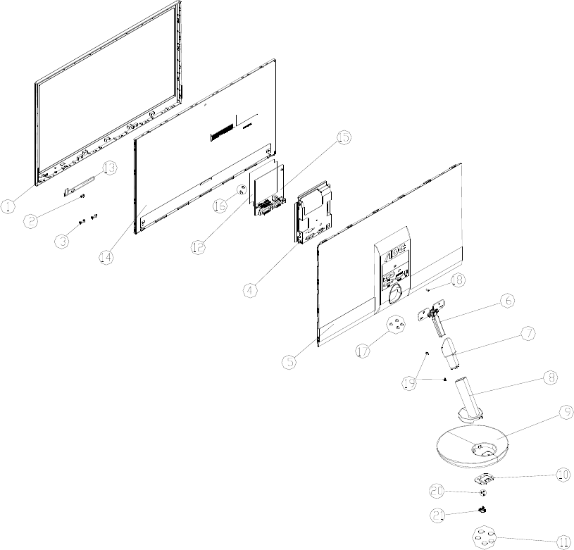
10. Monitor Exploded View

43
No. Description
1 BEZEL
2 Power lens
3 RUBBER FEET
4 Main frame
5 Rear cover
6 Hinge
7 Stand
8 Stand cover
9 Base No. Part No. Description
10 Stand plate 16 0D1G1030--8120 SCREW(MAIN BOARD/MAIN FRAME)
11 RUBBER FOOT 17 0Q1G-140-10120 SCREW(REAR COVER/HINGE)
12 MYLAR 18 0M1G3130--5-47-CR3 SCREW(REAR COVER/MAIN FRAME)
13 KEY BOARD 19 0M1G1730--8225-CR3 SCREW(STAND/HINGE)
14 PANEL 20 0Q1G1030--6120 SCREW(STAND PLATE/BASE)
15 MAIN BOARD 21 F01G6064--4 SCREW(STAND PLATE/HINGE)

44
11. BOM List
Note: The parts information listed below are for reference only, and are subject to change without notice. Please go
to http://cs.tpv.com.cn/hello1.asp for the latest information.
TIBJT32CB7SUHNF.LF
点位 组件 对象描述 备注
040G-58162435A P/N LABEL FOR MANUAL PE BAG
040G-58162461A Energy star label
040G-581689-4A BARCODE LABEL FOR 1 (58x35mm)
052G---1210--A 80MM * 25MM
052G---2191--A PAPER TAPE
052G6019--1 INSULATING TAPE
E08902 089G-725CAA-DB SINGAL CABLE 1500MM COMLINK
089G-725HAA-DB SINGAL CABLE 1500MM HONGLIN 2nd SOURCE
089G-725GAA-DB SINGAL CABLE 1500MM GREATLAND 2nd SOURCE
E08903 089G1745CAA-AC DVI CABLE 1500MM COMLINK
089G1745HAA-AC DVI CABLE 1500MM HONGLIN 2nd SOURCE
089G1745GAA-AC DVI CABLE 1500MM GREATLAND 2nd SOURCE
0D1G1030--8120 screw
0M1G1730--8225-CR3 screw(Hinge)
0M1G3130--5-47-CR3 SCREW M3 x5
0Q1G-140-10120 SCREW
0Q1G1030--6120 SCREW
708GBG01-CP-3A AOC 40(2200)
Q45G--77--4 PE FILM
Q50G---4-10 TIE (Y1900221)
Q52G---1185-98 3M TAPE
E750 750GBT215W4BB1N20
0 PANEL BM215WF4-T2BB
750GBT215W4BB1N10
0 PANEL BM215WF4-T2BB 2nd SOURCE
2436L-2518B BM215WF4-T2BB-632

45
3110T-0856A GALVALUME, T=0.3,BM215WF4-TJA1-6F1-A0,
Up
3110T-0856B GALVALUME, T=0.3,BM215WF4-TJA1-6F1-A0,
Down
3850L-0088A ID, YUPO, 78X37
4296L-0284B PMP-P2 100-520U-13, 5U-C60 black A600,
170x7x0.45
6060L-2569A LM215WF4(TJBA,T2BB)
6061L-2064A LM215WF4-TJAA
0ILUL-0185A LS0609D3-C6LS, LUSEM, 960, 6BIT, MINI, C_B,
R/TP, 48MM, 4PF, UPILEX, T9
6308L-4013A LTBXNSSNXX1-02150T01, 487.1*277.5,
LGC,T,B,X,N,S, S,N,X,X,1,02150,Top,01
6308L-4014A LTXXNSSNXX1-02150B01, 487.10*277.5, LGC,
T, X, X, N, S, S, N, X, X, 1, 02150, Bottom, 01
6871L-2552B Source, Single, None-C/SKD, LM215WF4-TJC1,
Single Side
C115 0CH2103K562 10NF, K, 50V, X7R, 0.9mm, 1608, R/TP
C915,C916 0CH2104H942 0.1uF, Z, 25V, Y5V, 0.9mm, 1608, R/TP
C1,C2,C302,C
5,C51,C6,C7,C
8,C924
0CH2104K562 0.1UF 50V K X7R 1608 R/TP
C79,C911 0CH2473H562 47nF, K, 25V, X7R, 0.9mm, 1608, R/TP
C56,C57,C74 0CH2473K562 47NF 50V K X7R 1608 R/TP
C3,C36,C4,C9
08 0CH2A-0007A 1U F, 10 Volt, K PER, X5R(JB), 1608 R/TP,
T=0.9(MAX)
C50,C55,C58,
C59 0CH2A-0010A 33nF, M, 25V, X7R, 0.9mm, 1608, R/TP
C22,C23,C32,
C33,C34 0CH2A-0011A 10U F, 16 Volt, K PER, X5R(JB), 3216 R/TP,
T=0.95(MAX)
C101,C102,C1
03,C104,C105,
C106,C107,C1
08,C109,C110,
C111,C112,C1
13,C114,C301,
C303,C305,C3
07,C309,C311,
0CH2A-0015A 1uF, K, 25V, X5R, 0.9mm, 1608, R/TP

46
C77,C907
C73 0CH2A-0017A 2.2U F, 10 Volt, K PER, X5R(JB), 1608 R/TP,
T=0.9(MAX)
C313,C314,C3
15,C318,C52,
C61,C62,C63,
C64,C71,C72,
C913,C914,C9
20,C921
0CH2A-0026A 10U F, 25 Volt, K PER, X5R(JB), 3225 R/TP,
T=1.0(MAX)
C312 0CH2A-0038A 0.1U F, 25 Volt, Z PER, Y5V(JF), 1005 R/TP,
T0.55(MAX)
C701 0CH2A-0049A 1.5nF, 50, -10~+10(K), 1608, X7R(JB)
C75 0CH2A-0088A 3.3nF, K, 50V, X7R, 0.9mm, 1608, R/TP
C912 0CH2A-0091A 1uF, K, 25V, X5R, 0.6mm, 1005, R/TP
D3,D4,D5 0DHZL-0008B BAV99-7-05-F, DIODES, SOT-23, R/TP
ZD1 0DHZL-0061A SDZ6V2D, AUK, SOD-323, R/TP
D6 0DHZL-0095A RB050M-30, ROHM, PMDU, R/TP
F1 0FFST-0002A F0603FA2500V032T, AEM, 2.5, 32 Volt,
1.6X0.8X0.8, SMT, Ceramic, UL/CSA
U3 0IDIL-0002A AP7167-FNG-7, DIODES, ADJUST_3.3V, 1.2A,
DFN3030-10, R/TP, 10
UC2 0IIML-0004A iML7821BE, IML, 5V~20V, 320mA, 20V/us,
40MHz, 1Ch, TSOT, R/TP, 5Pin
U4 0ISGL-0008C M24C04-RDW, STmicroeletronics, 4K, 5ms,
TSSOP, R/TP, 8
US2 0ISML-0007A
SM4025, SILICON MITUS, MONITOR,
BOOST+L/S(GPM)+OP-AMP+PVCOM+DISCHA
RGING,
UC1 0ISWL-0078A SW0640, SIW, LVDS, 6/8, 2, MINI-LVDS, 6, 1,
DRD, GIP, AFRC, DGA, MUTE, MLF, TR, 68
L1 0LCAA-0069B
TNI8016-100M, DACOWELL, 10UH, M=20%,
2.1A, 0.093, 8.0X11.0X1.8 (1.2MM, IN-BOARD),
R/TP
FL4,FL5,R103,
R109,R118,R1
19,R121,R125,
R126,R127,R1
29,R138,R139,
0RH0000C622 0 OHM 1/16W 1608 5% D R/TP

47
R140,R142,R1
79,R180,R20,
R302,R54,R60
1,R602,R801,
R802,R901,R9
02,R903,R906,
R908
R131 0RH0102C422 10 OHM 1/16W 1608 1% D R/TP
R701 0RH0221C622 2.2 OHM 1/16W 1608 5% D R/TP
R10,R11,R12,
R13,R14,R15,
R16,R17,R18,
R19,R22,R23,
R25,R26
0RH0302C422 30 OHM 1/16W 1608 1% D R/TP
R322 0RH0472C422 47 OHM 1/16W 1608 1% D R/TP
R2,R3 0RH1000C422 100 OHM 1/16W 1608 1% D R/TP
R1 0RH1001C422 1K OHM 1/16W 1608 1% D R/TP
R24,R55 0RH1002C422 10K OHM 1/16W 1608 1% D R/TP
R123,R225,R2
35,R244,R255 0RH1102C422 11K OHM 1/16W 1608 1% D R/TP
R214 0RH1201C422 1.2K OHM 1/16W 1608 1% D R/TP
R212 0RH1202C422 12K OHM 1/16W 1608 1% D R/TP
R211 0RH1301C422 1.3K OHM 1/16W 1608 1% D R/TP
R150 0RH1500C422 150 OHM 1/16W 1608 1% D R/TP
R151,R242,R2
7 0RH1502C422 15K OHM 1/16W 1608 1% D R/TP
R114,R136 0RH1601C422 1.6K OHM 1/16W 1608 1% D R/TP
R130,R233,R7
77 0RH1602C422 16K OHM 1/16W 1608 1% D R/TP
R141 0RH1800C422 180 ohm, 1/16W, 1608, 1%, R/TP
R115 0RH2201C422 2.2K OHM 1/16W 1608 1% D R/TP
R50,R51 0RH2401C422 2.4K OHM 1/16W 1608 1% D R/TP
R904 0RH2402C422 24K OHM 1/16W 1608 1% D R/TP
R101,R104,R1
06,R261 0RH2700C422 270 OHM 1/16W 1608 1% D R/TP

48
R243,R253 0RH2702C422 27K OHM 1/16W 1608 1% D R/TP
R148,R223,R2
34,R245 0RH3302C422 33K OHM 1/16W 1608 1% D R/TP
R135 0RH3602C422 36K 1/16W 1% 1608
R201 0RH3900C422 390 OHM 1/16W 1608 1% D R/TP
R146 0RH3902C422 39K OHM 1/16W 1608 1% D R/TP
R324,R326,R6
7 0RH4700C422 470 OHM 1/16W 1608 1% D R/TP
R202 0RH4702C422 47K OHM 1/16W 1608 1% D R/TP
R110,R132,R7
78,R905 0RH5101C422 5.1K OHM 1/16W 1608 1% D R/TP
R117 0RH5102C422 51K OHM 1/16W 1608 1% D R/TP
R203 0RH5600C422 560 ohm, 1/16W, 1608, 1%, R/TP
R122,R124,R4
,R5,R909 0RH5601C422 5.6K OHM 1/16W 1608 1% D R/TP
R222 0RH5602C422 56K OHM 1/16W 1608 1% D R/TP
R252 0RH6201C422 6.2K OHM 1/16W 1608 1% D R/TP
R254 0RH6202C422 62K OHM 1/16W 1608 1% D R/TP
R232 0RH7502C422 75K ohm, 1/16W, 1608, 1%, R/TP
R21,R231,R24
1,R251 0RH8201C422 8.2K OHM 1/16W 1608 1% D R/TP
R221 0RH9101C422 9.1K OHM 1/16W 1608 1% D R/TP
R910 0RH9102C422 91K OHM 1/16W 1608 1% D R/TP
R224 0RHAA-0015A 43K ohm, 1/16W, 1608, 1%, R/TP
AR5,AR6 0RHZL10005A 100OHM 5 1/16W 3216 R/TP
Q2 0TRRL-0010A KTA1505S-Y-RTK/H, KEC, PNP, R/TP, SOT-23, .
0TRRL-0019A MMBT4403, Diodes, PNP, R/TP, SOT-23, H/F, 3 2nd SOURCE
Q1 0TRRL-0011A KTC3876S-Y-RTK/H, KEC, NPN, R/TP, SOT-23, .
0TRRL-0020A MMBT4401, Diodes, NPN, R/TP, SOT-23, H/F, 3 2nd SOURCE
FL6,FL7,FL8,F
L9 6200L-J015A BLM18PG300SN1D
RT1 6322L-0004A 22K ohm, +-3%, 125, 0.21, 3950, 1608, R/TP

49
CN1 6630L-0157B FI-XB30SL-HF10, JAE, 30 Pin, 1 mm, Angle, Sn,
USER LOCK
6630L-0410A IS100-L30F-C15, UJU, 30 Pin, 1 mm, Angle, Sn,
USER LOCK 2nd SOURCE
6870S-1235A LM215WF4-TJC1-611, 2L, 0.6, 479.15*122.15, 3,
N, Source, NO, Single Side
E2436L 6091L-1904D BM215WF4-T2AA
6091L-1904B BM215WF4-T2AA 2nd SOURCE
3022L-1413A KOLON, XC210, T=0.123,
BM215WF4-TJA1-6F1-A0
3022L-1413B LUCKY, CDX131, T=0.21, BM215WF4-TJA1
3550B-0918A AL, T=0.5, BM215WF4-TJA1-6F1-A0
3850L-0151A BL, YUPO, 77X21
4975L-0464A BM215WF4-TJA1-6F1-A0
4974L-0864A PC,ENTIRE,ETR-1010,V0,
BM215WF4-TJA1-6F1-A0
5022L-0302A SH140U+5256M, SILICON, Gray, 274.7*2.0*0.4
5022L-0303A SH140U+5256M, SILICON, Gray, 485*2.0*0.4
5151L-0218A BM215WF4-TJA1-6F1-A0
3034L-0937A TORAY, TZC25S, T=0.25, 3M, 1363-60,
BM215WF4-TJA1-6F1-A0
3953L-0217A TORAY, 188E60L, T=0.188, 3M, 1363-60,
441.7*1.8*0.2, BM215WF4-TJA1-6F1-A0
3953L-0218A TORAY, 188E60L, T=0.188, 3M, 1363-60,
286*1.8*0.2, BM215WF4-TJA1-6F1-A0
5150L-0595A PMMA, Flat, 2.0, Printing,
BM215WF4-TJA1-6F1-A0
6916L-0539C EverTop, LED, 32(Number Of LED), White LED,
BM215WF4-TJA1
5153L-0068A 10FH-SM1-GAN-TB(LF)(SN) , JST
6915L-0284C Ever Top LED,WM32NW1F,Top View,2ea(LED
Chip Q'TY per PKG), 7020PKG
6920L-0064A 283.4*4.2*1.2, 2ea(Number Of Chain), 1L(Number
Of Layer), 32ea(Number Of LED), AL
7250L-1401B TP-15;282.6*3.6*0.25T
7250L-0864A NITTO, NITTO 5000NS, Clear, 30*3*0.16

50
7250L-1408A ZH350 25x16x0.1
7250L-1488B Conductive Tape,STN1026WR(P), T=0.11,
15*25*0.11
756GFBCB-AA016--00 MAINBOARD-CBPCAT3A1AX
SMTCA-U403 100GARJI004FT1 MCU ASS’Y-056G2233-11
A15G1636101 MAIN_FRAME
A15G1648101 PlATE
A33G1203AED-1B0100 stand-top
A33G1204--1-1C0100 Power lens
A34G2579AEDD1B013
0 BEZEL
A34G2580AED-1B0100 rear cover
A34G2581AED-1B0100 Stand-cover
A34G2618AED-1B0130 BASE
A37G0252011 HINGE
CN406 033G801930F-CH---L WAFER 30P 1.0MM XIANGLONG
033G801930F-CH--JS WAFER 30P 1.0MM JINGSHI 2nd SOURCE
C716 067G204V471-2L CS CAP 470uF +-20% 10V 8*8 LELON
067G204V471-2K CS CAP 470uF 10V 8*8 mm 2nd SOURCE
C718,C811 067G215C151-4H EC 150uF +-20% 25V 8*7mm 700mA 2000Hr
HER MEI
C807 067G415R479-9L EC 4.7UF 20% 100V RZW 8*12
067G415R479-9K EC 4.7UF 20% 100V ED 8*12 2nd SOURCE
FB701 071G--5526A--H CORE 6.0X3.5X3.5 127 25% 3.5X6.0
071G--5526A--S CORE 6.0X3.5X3.5 127 25% 2nd SOURCE
CN101 088G-35315FVXH D-SUB CONN WITH SCREW 15P BLUE
XIANHE
088G-35315FVCL D-SUB CONN WITH SCREW 15P BLUE CL 2nd SOURCE
CN102 088G354GOF1VXH DVI CONN WITH SCREW 24P WHITE XIANHE
X401 093G--22-53--J Diode CRY 14.31818MHZ/32PF/49US NSK
709G4798-QM001 COMSUPTIVE ASS""Y

51
055G--23524--A WELDING FULX WITHOUT Pb
Q49G--51100 GW2066 Cleaner
Q55G-100625 TIN STICK_LOW ARGENTUM
C141,C707 F67G305M1013GV 100uF +-20% 16V 105 ℃ 2000H 6.3*7
067G305S1013HV EC 100UF 20% 16V 6.3*7 2nd SOURCE
CN701 F88G-304-11-YG DC JACK 3P BLACK YCG
088G-304-11--C DC JACK 3P BLACK CL 2nd SOURCE
CN803 033G801910Y--H NO-SUGGEST WAFER 10P 0.5MM GAOLIN
311GF050B10ADH FFC CONN 10P 0.5MM HR 2nd SOURCE
U401 056G-562434 IC SCALER RTD2281W-CG QFP-128 Realtek
U702 056G-563512--C IC LDO G1117-33PT43U 1A 3.3V TO-252 GMT
056G-563512 NO-SUGGEST IC LDO G1117-33T43UF 1A/3.3V
TO-252 GMT 2nd SOURCE
056G-563520 NO-SUGGEST IC LDO LSP1117D33AG 1A 3.3V
TO-252 LITEON 2nd SOURCE
U102,U103,U1
04,U106,U107 056G-662-48 IC ESD PROTECT AZC399-04S SOT23-6L
AMAZING
056G-662-49 NO-SUGGEST IC ESD PROTECT
L30ESDL5V0C6-4 SOT23-6L LITEON 2nd SOURCE
U801 056G-700--5 IC LED DRIVER MP3389EF TSSOP28 MPS
U101,U105 056G1133158 IC EEPROM CAT24C02WI-GT3A 2Kb SOIC-8
ON
056G1133531 NO-SUGGEST IC EEPROM FM24C02A-SO-T-G
2K SOP-8 FUDAN 2nd SOURCE
056G1133-34--1 IC EEPROM M24C02-RMN6TP 2Kb SO-8 ST 2nd SOURCE
U403 056G2233-11 IC FLASH Pm25LD020C-SCE SIOC-8 2M PMC
Q402,Q404 057G-417517 TRA LMBT3906LT1G -0.2A/-40V SOT-23 LRC
057G-417512 TRA MMBT3906 0.2A/40V SOT-23 BLUE
ROCKET 2nd SOURCE
Q701,Q706 057G-417518 TRA LMBT3904LT1G 0.2A/40V SOT-23 LRC
057G-417511 TRA MMBT3904 0.2A/40V SOT-23 BLUE
ROCKET 2nd SOURCE
Q806 057G-763-92 MOSFET P8008HV 4A/80V SOP-8 NIKO-SEM

52
Q705 057G-763535 MOSFET LP3401LT1G -4.2A/-30V SOT-23 LRC
057G-763940 MOSFET AO3401A 4.2A/30V SOT-23 AOS 2nd SOURCE
R419,R421,R4
24,R425,R439,
R444,R448,R4
52,R453,R483
061G0402000-JT RST CHIPR MAX0R05 1/16W TZAI YUAN
R104,R109,R1
16,R131,R132,
R133,R134,R1
35,R136,R137,
R138
061G0402100-JT RST CHIPR 10 OHM +-5% 1/16W 0402 TZAI
YUAN
R120,R121,R4
22,R479,R480,
R481,R482,R7
06
061G0402101-JT RST CHIPR 100 OHM +-5% 1/16W 0402 TZAI
YUAN
R127,R142,R1
49,R150 061G0402102-JT RST CHIPR 1 KOHM +-5% 1/16W 0402 TZAI
YUAN
R416,R428,R4
35,R702,R703,
R719
061G0402103-JT RST CHIPR 10 KOHM +-5% 1/16W 0402 TZAI
YUAN
R437,R712,R7
21,R804 061G0402104-JT RST CHIPR 100 KOHM +-5% 1/16W 0402 TZAI
YUAN
R427,R429,R4
31,R433 061G0402220-JT RST CHIPR 22 OHM +-5% 1/16W 0402 TZAI
YUAN
R122,R123,R4
45 061G0402222-JT RST CHIPR 2.2 KOHM +-5% 1/16W 0402 TZAI
YUAN
R720 061G0402223-JI RST CHIPR 22 KOHM +-5% 1/16W 0402 TA-I
R114,R130,R7
04 061G0402223-JT RST CHIPR 22 KOHM +-5% 1/16W 0402 TZAI
YUAN
R438 061G0402224-JT RST CHIPR 220 KOHM +-5% 1/16W 0402 TZAI
YUAN
R726 061G0402303-JT RST CHIPR 30 KOHM +-5% 1/16W 0402 TZAI
YUAN
R711,R803,R8
19 061G0402333-JT RST CHIPR 33 KOHM +-5% 1/16W 0402 TZAI
YUAN
R436 061G0402394-JF RST CHIPR 390 KOHM +-5% 1/16W 0402
FENGHUA
R101,R105,R1
07,R111,R118,
R125,R126,R4
061G0402470-JT RST CHIPR 47 OHM +-5% 1/16W 0402 TZAI
YUAN

53
77,R478
R112,R113,R1
28,R129,R415,
R420,R451,R4
59,R467,R475,
R476,R705,R7
18
061G0402472-JT RST CHIPR 4.7 KOHM +-5% 1/16W 0402 TZAI
YUAN
R106,R110,R1
17 061G0402750-JT RST CHIPR 75 OHM +-5% 1/16W 0402 TZAI
YUAN
FB101,R119,R
455 061G0603000-JT RST CHIP MAX 0R05 1/10W TZAI YUAN
R713 061G0603100-JT RST CHIPR 10 OHM +-5% 1/10W 0603 TZAI
YUAN
R714 061G06031002FF RST CHIPR 10 KOHM +-1% 1/10W 0603
FENGHUA
R806,R808 061G0603102-JT RST CHIPR 1 KOHM +-5% 1/10W 0603 TZAI
YUAN
R827,R830 061G0603109-JT RST CHIPR 1 OHM +-5% 1/10W 0603 TZAI
YUAN
R811 061G0603151-JT RST CHIPR 150 OHM +-5% 1/10W 0603 TZAI
YUAN
R446 061G0603201-JT RST CHIPR 200 OHM +-5% 1/10W 0603 TZAI
YUAN
R807,R810 061G0603203-JT RST CHIPR 20 KOHM +-5% 1/10W 0603 TZAI
YUAN
R841,R842 061G0603229-JT RST CHIPR 2.2 OHM +-5% 1/10W 0603 TZAI
YUAN
R802,R834 061G06032703FF RST CHIPR 270 KOHM +-1% 1/10W 0603
FENGHUA
R715 061G06035362FF RST CHIPR 53.6KOHM +-1% 1/10W 0603
FENGHUA
R430,R809 061G06036201FF RST CHIPR 6.2 KOHM +-1% 1/10W 0603
FENGHUA
R801 061G0805100-JT RST CHIP 10R 1/8W 5% TZAI YUAN
R805 061G0805304-JT RST CHIP 300K 1/8W 5% TZAI YUAN
R813 061G12060004JT RST CHIP MAX 0R05 1/4W TZAI YUAN
R812 061G12061207FF RST 1206 0.12R 1% 1/4W FENGHUA
R146,R147 061G1206301-JT RST CHIPR 300 OHM 1/4W TZAI YUAN

54
R843 061G1206681-JT RST CHIPR 680 OHM +-5% 1/4W
C404,C405,C4
06 065G040210131J---Y MLCC 0402 100pF +-5% 50V NPO YAGEO
C113,C114,C1
15,C117,C118,
C119,C142,C4
02,C403,C408,
C409,C410,C4
11,C414,C417,
C419,C422,C7
08,C709,C717,
C721,C725
065G040210412K---A MLCC 0402 0.1uF +-10% 16V X7R SAMSUNG
C416,C420 065G0402105A5K---A MLCC 0402 1uF +-10% 10V X5R SAMSUNG
065G0402105A5K---T MLCC 0402 1uF -10% 10V X5R TAIYO YUDEN 2nd SOURCE
C145,C146,C1
51,C415,C418,
C731
065G040222031J---T MLCC 0402 22pF +-5% 50V NPO TAIYO YUDEN
C722 065G040222232K---Y MLCC 0402 2.2nF +-10% 50V X7R YAGEO
C147 065G040222322K---Y MLCC 0402 22nF +-10% 25V X7R YAGEO
C101,C116,C4
12,C724 065G040222415K---T MLCC 0402 0.22uF +-10% 16V X5R TAIYO
YUDEN
C102,C104,C1
05,C107,C108,
C110
065G040247312K---A MLCC 0402 47nF +-10% 16V X7R SAMSUNG
C103,C106,C1
09 065G040250931C---Y MLCC 0402 5pF +-0.25pF 50V NPO YAGEO
C710,C714,C8
05,C806,C809,
C815
065G060310131J---A MLCC 0603 100pF +-5% 50V NPO SAMSUNG
065G060310131J---M MLCC 0603 100pF -5% 50V NPO MURATA 2nd SOURCE
C715 065G060310232K---Y MLCC 0603 1000pF +-10% 50V X7R YAGEO
C712,C719,C8
10,C812 065G060310432K---Y MLCC 0603 0.1uF +-10% 50V X7R YAGEO
C713,C728 065G060310525K---T MLCC 0603 1uF +-10% 25V X5R TAIYO YUDEN
065G060310525K---3
NO-SUGGEST MLCC 0603 1uF -10% 25V X5R
TDK 2nd SOURCE
C801 065G060347412K---A MLCC 0603 0.47uF +-10% 16V X7R SAMSUNG

55
065G060347412K---T
MLCC 0603 0.47uF -10% 16V X7R TAIYO
YUDEN 2nd SOURCE
C802 065G060368332K---Y MLCC 0603 68nF +-10% 50V X7R YAGEO
C413,C424,C4
25 065G0805106A5K---A MLCC 0805 10uF +-10% 10V X5R SAMSUNG
065G0805106A5K---T
MLCC 0805 10uF -10% 10V X5R TAIYO
YUDEN 2nd SOURCE
C813,C814 065G080522232K---Y MLCC 0805 2200pF +-10% 50V X7R YAGEO
C803,C804 065G080547432K---T MLCC 0805 0.47uF +-10% 50V X7R TAIYO
YUDEN
065G080547432K---M MLCC 0805 0.47uF -10% 50V X7R MURATA 2nd SOURCE
C720,C723 065G120610625K---A MLCC 1206 10uF +-10% 25V X5R SAMSUNG
065G120610625K---T
MLCC 1206 10uF -10% 25V X5R TAIYO
YUDEN 2nd SOURCE
U403 070GHDCP500HDC HDCP CODE
FB102,FB403,
FB404,FB702 071G-56K121--M CHIP BEAD
FB408 071G-59C121-TA CHIP BEAD 0603 120R 25% 300mA
FCM1608CF-121T03 TAI-TECH
071G-59C121--B FCM1608C-121T03 SMD 2nd SOURCE
FB103 071G-59G301-TA CHIP BEAD 300OHM 200mA
FCM1608KF-301T02
FB104,FB105,
FB106 071G-59K190-TA CHIP BEAD 0603 19R 25% 500mA
FCB1608KF-190T05 TAI-TECH
071G-59K190--B 19 OHM BEAD 2nd SOURCE
L801 073G253S-98-DN SMD CHOKE 47uH 20% 3A 64R
073G253S-98--X SMD CHOKE 47UH 20% 0.064R
3SMSL12575-470 2nd SOURCE
L701 073G253S521--H SMD CHOKE 22UH 20% 3.3A HF
073G253S521--M SMD CHOKE 2nd SOURCE
D101,D102 093G--64-42--L DIODE LBAV70LT1G 0.15A/75V SOT-23 LRC
093G--64-42--P DIODE BAV70 0.5A/100V SOT23 PANJIT 2nd SOURCE
D401,D403,ZD
101,ZD102,ZD
105,ZD106
093G-39GA01--T DIODE ZD RLZ5.6B 5.6V/0.5W SEMTECH

56
ZD703 093G-39GA52--T DIDOE ZD ZM-PTZ9.1BST 9.1V/1W LL-41
SEMTECH
D801 093G-60S907--T Diode SCHOTTKY B3100B 3A 100V SMB
LITEON
D701 093G3004--2 DIODE SCHOTTKY SR34 3A/40V SMB PANJIT
CN405 311GF100C06ADH FFC CONN 6P 1.0mm HR
U705 356G0563419 IC LDO DC/DC APW7089KAI-TRG 4A 26V
SOP-8P ANPEC
056G-563513 NO-SUGGEST IC LDO APW7080KAITRG 4A/26V
SOP-8P ANPEC 2nd SOURCE
709G4798-QS001 COMSUPTIVE ASS""Y
052G---2191--A PAPER TAPE
E715 715G4798M01000004L MAIN PCB FR-4 92*102mm*1.6mm 6
715G4798M01000004S MAIN PCB FR-4 92*102mm*1.6mm 6 2nd SOURCE
715G4798M01000004I MAIN PCB FR-4 92*102mm*1.6mm 6 2nd SOURCE
715G4798M01000004F MAIN PCB FR-4 92*102mm*1.6mm 6 2nd SOURCE
F12G6300001 RUBBER
F12G6600001 RUBBER FEET
F40G-22E61518A Rating Label for E2251SWDN-e2251Swn 迪拜
Fire bird
F40G000361511C Warning Label for e51 WW WH
F44GBF01101 EPS for e2151vw
F44GBF01201 EPS for e2151vw
F44GBG01615-3A Carton for E2251SWDN
F52G1201163001 double sides adhesive tape
F52G1801499001 Mylar
F70G22C1615-4A E2251SWDN CD MANUAL
F80G-L19A10-HR Adapter 19V 1.7A 32W AOC HONOR
E08901 F89G604A15N-HL POWER CORD 1500MM Europe HONGLIN
089G604A15N-IS POWER CORD 1500MM Europe I-SHENG 2nd SOURCE
F89G604A15N-JR POWER CORD 1500MM EUROPE JIANRUN 2nd SOURCE
F95G176J-10103 FFC CABLE 10P 326MM P0.5MM KOTL

57
F95G176X-10103 FFC CABLE 10P 326MM P0.5MM WENXIN 2nd SOURCE
F09503 F95G179X30N102 FFC CABLE 30P 241MM P1.0MM WENXIN
F95G179J30N102 FFC CABLE 30P 241MM P1.0MM KOTL 2nd SOURCE
KEPCAAB5 KEY BOARD
F09501 F95G-76T--6603 FFC CABLE 6PIN 344MM 1.0MM DIY
F95G-76X--6603 FFC CABLE 6PIN 344MM 1.0MM WENXIN 2nd SOURCE
F95G-76J--6603 FFC CABLE 6PIN 344MM 1.0MM KOTL 2nd SOURCE
U001 056G-669-45 IC TOUCH KEY IT7230EFN/BX QFN16 ITE
R005,R006 061G0402000-JT RST CHIPR MAX0R05 1/16W TZAI YUAN
R004 061G0402101-JT RST CHIPR 100 OHM +-5% 1/16W 0402 TZAI
YUAN
R001 061G0402103-JT RST CHIPR 10 KOHM +-5% 1/16W 0402 TZAI
YUAN
R002,R003,R0
07,R008 061G0402472-JT RST CHIPR 4.7 KOHM +-5% 1/16W 0402 TZAI
YUAN
C008 065G040210131J---Y MLCC 0402 100pF +-5% 50V NPO YAGEO
065G040210131J---A MLCC 0402 100pF -5% 50V NPO SAMSUNG 2nd SOURCE
C005,C006,C0
07 065G040210427Z---Y MLCC 0402 0.1uF -20%+80% 25V Y5V YAGEO
065G040210427Z---T
MLCC 0402 0.1uF -20% 80% 25V Y5V TAIYO
YUDEN 2nd SOURCE
C011 065G0402105A5K---A MLCC 0402 1uF +-10% 10V X5R SAMSUNG
065G0402105A5K---T MLCC 0402 1uF -10% 10V X5R TAIYO YUDEN 2nd SOURCE
C003,C004 065G040212031J---Y MLCC 0402 12pF +-5% 50V NPO YAGEO
065G040212031J---A MLCC 0402 12pF -5% 50V NPO SAMSUNG 2nd SOURCE
D001 081G15BY--2-GP CHIP LED blue/Orange GPTD12048BOC1-A
GUANGPU
081G15BY--2-EL LED Blue/Orange 12-22/BHS2C-C30/2C
EVERHIGHT 2nd SOURCE
ZD001,ZD002 093G-39S501--T DIODE ZD LUDZS5.6BT1G 5.6V/0.5W SOD-323
LRC
093G-39S-34--T NO-SUGGEST Diode ZD UDZSNP5.6B ROHM 2nd SOURCE
709G4842-QS001 COMSUPTIVE ASS""Y

58
E715 715G4842K01000004S Key Board FR-4 105*11*1.2mm 16
715G4842K01000004F Key Board FR-4 105*11*1.2mm 16 2nd SOURCE
715G4842K01000004L Key PCB FR-4 105*11*1.2mm 16 2nd SOURCE
Q12G6600--6 FOOT
Q40G000161514A CARTON LABEL(70*80)
Q40G0001624-4A PALLET LABEL
Q41G78D1615-9A WARRANTY CARD
Q45G2010M0201A pe bag for manual
Q45G8801607--7 pe bag
