Applied Micro Design 1473PA-HE-400 Model 1473 Head End Power Amplifier User Manual
Applied Micro Design, Inc Model 1473 Head End Power Amplifier
User Manual
Montclair State University
MSU Head End System
Channelized Bi-Directional Amplifer
User’s Manual
rev 2
ETHERNET
TEMP FLT
STATUS
PA CUR
LNA CUR
FWD PWR
FAN FLT
KEY
REFL PWR
PA CUR FLT
LNA CUR FLT POWER
IN/OUT
RF OUT
400 MHz AMPLIFIER/LNA
MODEL 1473PA
RF IN
AMPLIFIER
DUPLEXER
LNA
SAMPLE
PORT
ETHERNET
FLT
FLT
PWR
FLT
FLT
RF OUT
RF IN
TX
STATUS
RX
1
1
1
2
2
2
RF OUT
RF IN
TX
STATUS
RX
1
1
1
2
2
2
SUPPLY
POWER
POWER
CC1
CC2
CC3
CC4
Table of Contents
Notes, Cautions, and Warnings
Description
Block Diagram
Specifications
Features
Uplink
Downlink
2

Notes, Cautions, and Warnings
3
This is a Class B Booster.
!Invisible laser light is used on these equipment.
DO NOT look directly into the fiber optic connectors when unit is in operation.
Connect RF Output to existing Distributed Antenna System (DAS) cable only.
DO NOT operate equipment with unauthorized antennas, cables, and/or coupling
devices.
DO NOT operate equipment unless all RF connectors are secure.
DO NOT operate equipment unless it has been installed and inspected by a qualified
radio technician.
Contact Information
For more information contact the FCC at:
https://signalboosters.fcc.gov/signal-boosters/
F.2 PART 90 CLASS B SIGNAL BOOSTERS Licensees and signal booster operators are
required to register existing Class B signal booster installations with the FCC by November
1, 2014. After November 1, 2014, operation of an existing, unregistered Class B signal
booster will be unauthorized and subject to enforcement action. Any new Class B signal
booster installed after November 1, 2014 must be registered prior to operation. To
encourage compliance with this new requirement, registration will be free of cost to the
operator and/or licensee.[R11], [R9]
FCC Part 90 Class B Signal Booster Registration & Discovery website:
https://signalboosters.fcc.gov/signal-boosters/
Part 90 (Class B) Signal Boosters
WARNING. This is NOT a CONSUMER device. It is designed for installation by FCC
LICENSEES and QUALIFIED INSTALLERS. You MUST have an FCC LICENSE or express
consent of an FCC Licensee to operate this device. You MUST register Class B signal
boosters (as defined in 47 CFR 90.219) online at www.fcc.gov/signal-booster/registration.
Unauthorized use may result in significant forfeiture penalties, including penalties in excess of
$100,000 for each continuing violation.
Description
4
There are two major elements to the MSU system; the Head End (HE) hardware and the Remote
Hardware. There is one HE and multiple remotes.
Each Remote consists of a single Fiber-Fed Power Amplifier chassis. The Remote chassis
contains a Down Link Power Amplifier, and Up Link LNA, and a Fiber Optic Transmitter and
Receiver.
The Head End consists of a Fiber-Fed Power Amplifier (FFPA) chassis, a DSP Chassis, and Fiber
Optic Chassis. The FFPA chassis contains an Up Link Power Amplifier, a Down Link LNA, and a
Duplexer. The DSP Chassis contains one each Uplink and Down Link DSP filter cards. The Fiber
Optic Chassis contains a FO Transmitter and FO Receiver for each Remote
In the Uplink (UL) path, signals from portable radios are input to the Remote DAS. These signals
are amplified in a Low Noise Amplifier (LNA) and converted to light by a Fiber Optic Transmitter in
the Remote chassis, and transmitted to the Head End via fiber optic cable. In the Head End rack,
the light from the fiber optic cable is converted back to RF by a Fiber Optic Receiver; the RF is
filtered in the UL DSP Card and the filtered signal is input to the power amplifier module. The
amplified RF is fed to the outside antenna via a duplexer.
In the Downlink (DL) path, signals from user radios (Motorola radios that are FCC certified) are
input to the Head End LNA. These signals are filtered in the DL DSP Card, combined with signals
from a Motorobo repeater, converted to light by a HE Fiber Optic Transmitter, and transmitted to
the FFPA via fiber optic cable. In the Remote chassis, the light from the fiber optic cable is
converted back to RF by a Fiber Optic Receiver, and the RF is input to a power amplifier module.
The amplified RF is input to a bandpass filter; the filtered RF feeds the Distributed Antenna
System (DAS) in the building where the remote hardware is located.
A Sample Port on the front panel of the FFPA allows the user to sample the signal without
interrupting main line communications. The Sample Port is 40 dB below the main RF output port.
The FFPA has a processor board that monitors overall chassis operation. The processor board
controls the enable signal to the amplifier and monitors forward power, reverse power, current, fan
status and heat sink temperature. Forward and reverse power are derived from directional
couplers built into the amplifier modules.
Heat sink temperature is derived from a thermistor mounted onto the heat sink and amplifier
current from a sense resistor in series with the +28-volt power input. The fan has a built-in
stopped rotor line which is input to the processor board.
The processor board features optional remote monitoring capability via Ethernet. The Graphical
User Interface (GUI) of the Network Management System (NMS) computer can display the status
of the amplifier and provide control.
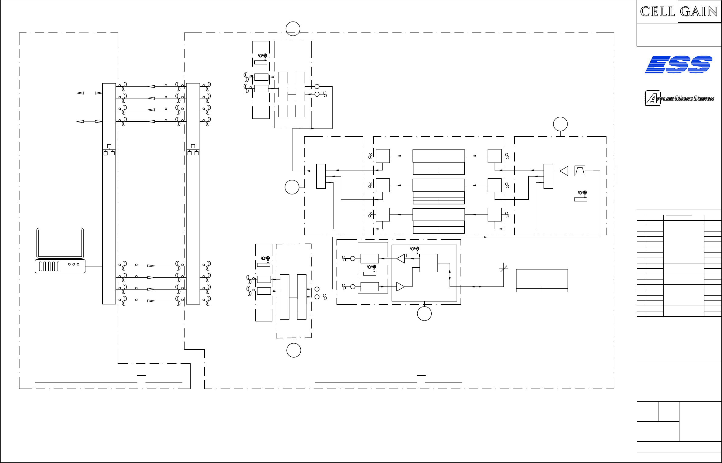
B
C
DSP-U
DSP-D
H
C
4
x
1
1
x
4
FOT
University Hall 8th
Floor
A2
C1
PA-2
HD 30676
S2
Tap
10dB
Property of MSU
(Repeater Rack)
Rx
Tx
RxTx
RxTx Mototrbo
Mdl.# XPR8400 Band1
Mototrbo
Mdl.# XPR8400 Band1
Mototrbo
Mdl.# XPR8400 Band1
1
x
3
D2
Antenna: A2
Telewave #ANT490Y10-WR or =
Little Falls Fire Dept.
Base Tx MHz (DL) Base Rx MHz (UL)
478.2500 481.2500
Fiber Optic Punch Panel
Fiber Optic Punch Panel
University Hall 6th
Floor
From Sixth Floor
From Sixth Floor
From Sixth Floor
To Sixth Floor
To Sixth Floor
To Sixth Floor
1
x
3Mini-Ckts.
LNA
ZFL-500HLN+
Model # 1473PA-X-X
µP
µP
Model #
1473SC-X-X
Model #
1473FOT
Model #
1456DSP
µP
G
H
1
x
4
1
x
4
FOR
FOR
C2 S1
Model #
1473SC-X-X
Model #
1473FOR
µP
Model # 1473LNA-X-XModel # 1473LNA-X-X
FOT
MSU Police
Base Tx MHz (DL) Base Rx MHz (UL)
461.9525 465.9625
MSU EMS
Base Tx MHz (DL) Base Rx MHz (UL)
460.3625 465.3625
MSU OEM
Base Tx MHz (DL) Base Rx MHz (UL)
461.5875 466.5875
From Sixth Floor
To Sixth Floor
to/from SBUS
to/from CELS
G-Way Microwave
CB466.3/3SK-E2N
G-Way Microwave
CD479.8/2SK-F3
LNA
Mini-Ckts.
ZFL-500HLN+
Combiner
Mini-Ckts.
ZBSC-413
Splitter
Mini-Ckts.
ZBSC-413
Combiner
Mini-Ckts.
ZBSC-413
Splitter
Mini-Ckts.
ZBSC-413
Power
Divider/Combiner
MECA
803-2-0.252
Power
Divider/Combiner
MECA
803-2-0.252
Tap
10dB
Tap
10dB
Tap
30dB
Tap
30dB
Tap
30dB
A
B
B
C
D
µP
68 WHITE
STREET #265
RED BANK,
NJ
732-889-4671
MSU
University Hall
Block Diagram
N/A
02/15/2016 1 of 1
Matt Jacobs
Site Name/Address:
Project:
Scale: Sheet #:
Date:
Drawn By:
Drawing #:
2/19 MTJ Removed FOT/R from
MSU line.
Added rack
demarcations.
Added freq. tables at
antennas.
Notated MSU ownership
of repeaters.
3/2 MTJ Added 8th to 6th
connection diagram
Revisions
Date Drawn By Aprvd. By
Revision Notes
3/5 MTJ Integrated AMDi Design
Changes
MSUHEBD001 rev.4
Sheet Size:
D
3/15 MTJ Removed EMR unit and
CD 481 unit. Added
CD479.8/2SK-F3
LNA&PA unit
5/03 MTJ Added Tap data to MSU
Radio
6
1473PA-HE and 1456DSP Block Diagram
DOWNLINK
478.2500 MHz
UPLINK
481.2500 MHz
LNA
PA
Model No.
1473PA-HE
µP
HD30676
Duplexer
G-Way Microwave
CD479.8/2SK-F3
ZFL-500HLN
DSP-U
DSP-D
Model No.
1456DSP
µP
System Specification
7
Specifications - PA/LNA
Uplink
Frequency: 481.2500 MHz
Type: Class AB
Bandwidth: 18 MHz
Gain: 40 dB
N.F.: 7 dB
Max. Power Output: 20 dBm
ALC: 30 dBm
Harmonics: > 60 dBc, 2nd and 3rd
OIP3: +55 dBm
Impedance: 50 Ohms
Load VSWR: Infinite, no damage
Downlink:
Frequency: 478.2500 MHz
Type: Linear
Bandwidth: 16 MHz
Gain: 19 dB
NF: 4 dB
Impedance: 50 Ohms
Input Level: -90 dBm to -10 dBm
Power Supply: 115 V AC
Current: < 2A
Operating Temp: -30° to +60° C
Size: 19” x 5.22” x 16”
* With fiber link gain of zero
Features
•power amplifier automatic level control (ALC)
•high power amplifier gain
•high power amplifier Third-Order Intercept Point (OIP3)
•sample port at 40 dBc
•channelized DSP filtering
•signal automatic gain control (AGC) via DSP
8
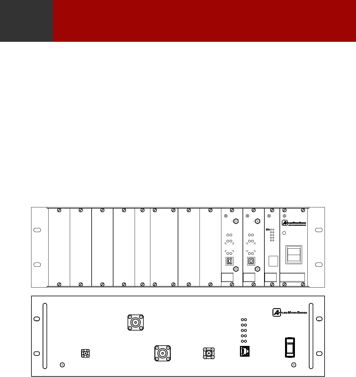
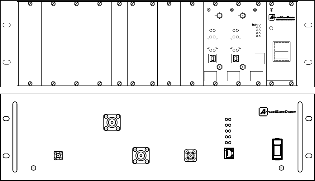
ETHERNET
TEMP FLT
STATUS
PA CUR
LNA CUR
FWD PWR
FAN FLT
KEY
REFL PWR
PA CUR FLT
LNA CUR FLT POWER
IN/OUT
RF OUT
400 MHz AMPLIFIER/LNA
MODEL 1473PA
RF IN
AMPLIFIER
DUPLEXER
LNA
SAMPLE
PORT
ETHERNET
FLT
FLT
PWR
FLT
FLT
RF OUT
RF IN
TX
STATUS
RX
1
1
1
2
2
2
RF OUT
RF IN
TX
STATUS
RX
1
1
1
2
2
2
SUPPLY
POWER
POWER
CC1
CC2
CC3
CC4
Power
Switch
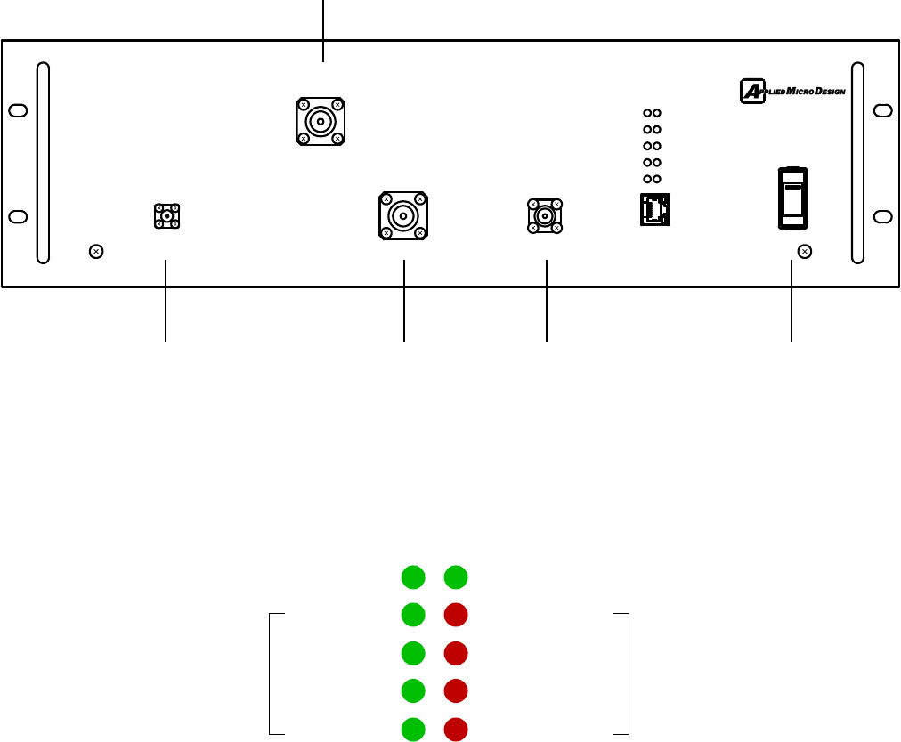
Duplexer Input/Output
Connector
LNA Output
Connector -40 dB
Sample Port 2
Connector
STATUS KEY
REFL PWR
LNA CUR FLT
FOR FLT
FAN FLT
FWD PWR
PA CUR FLT
FOT FLT
TEMP FLT
Head End PA/LNA - Front Panel and Indicators
Model No. 1473PA-HE
steady: amplifer/LNA is operating steady: amplifier is enabled
steady: amplifier or LNA is
operating normally steady: amplifier or LNA has
either current, reverse power or
temperature fault
Power Amplifier
Input Connector
9
ETHERNET
TEMP FLT
STATUS
PA CUR
LNA CUR
FWD PWR
FAN FLT
KEY
REFL PWR
PA CUR FLT
LNA CUR FLT POWER
IN/OUT
RF OUT
400 MHz AMPLIFIER/LNA
MODEL 1473PA
RF IN
AMPLIFIER
DUPLEXER
LNA
SAMPLE
PORT
10
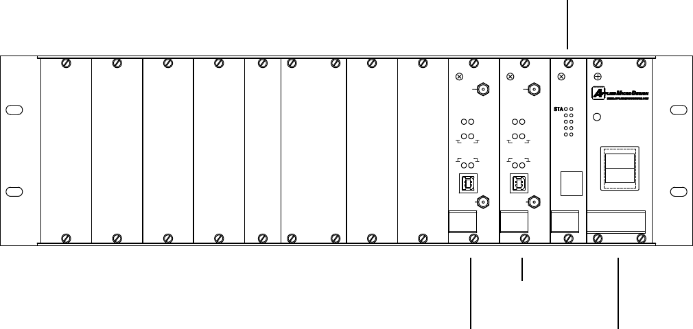
Card No.
2
Card No.
1
Processor
Card
Power
Supply
DSP - Front Panel
Model No. 1456DSP
ETHERNET
FLT
FLT
PWR
FLT
FLT
RF OUT
RF IN
TX
STATUS
RX
1
1
1
2
2
2
RF OUT
RF IN
TX
STATUS
RX
1
1
1
2
2
2
SUPPLY
POWER
POWER
CC1
CC2
CC3
CC4
11
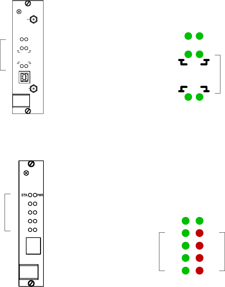
DSP Card
Processor Card
Status
Indicator
RF Output
Connector
USB
Connector
RF Input
Connector
Status
Indicators
STATUS
1 2
1 2
1 2
RX
TX
STA
CC1
PWR
FLT
FLT
FLT
FLT
blinking: unit is operating steady: unit is powered
steady: either current,
reverse power or
temperature fault
blinking: card is disabled
steady: card is enabled
L.E.D. columns blink alternately until processor card
establishes communication with DSP cards.
steady: board is initialized
steady: board is keyed
blinking: board is communicating
with processor card
RF OUT
RF IN
TX
STATUS
RX
1
1
1
2
2
2
DSP - Indicators
Model No. 1456DSP
ETHERNET
CC1
FLT
FLT
FLT
FLT
CC2
CC3
CC4
CC2
CC3
CC4
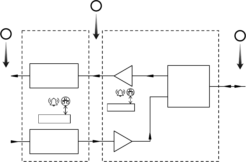
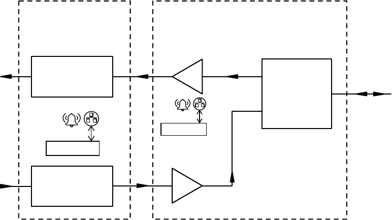
Downlink
The Downlink chain of the Head End consists of a Duplexer, a Low-Noise Amplifier (LNA) and
a digital signal processor (DSP) card. The RF signal is applied to “ A “ shown below at the
Duplexer Input/Output port.
The Duplexer separates the Downlink signals from the Uplink signals. The Downlink port of
the Duplexer is connected to the input of the LNA. The RF signal is amplified by the LNA and
comes out at a higher level at “ B. “ The RF signal from the LNA is fed into the DSP card for
filtering and level adjustment to ensure the signal level is always constant at “ C. “
A
B
C
12
LNA
PA
Model No.
1473PA-HE
µP
HD30676
Duplexer
G-Way Microwave
CD479.8/2SK-F3
ZFL-500HLN
DSP-U
DSP-D
Model No.
1456DSP
µP
13
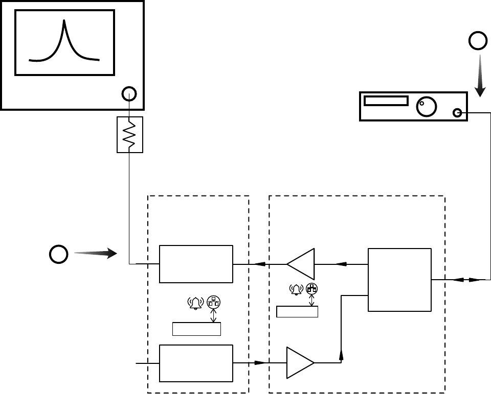
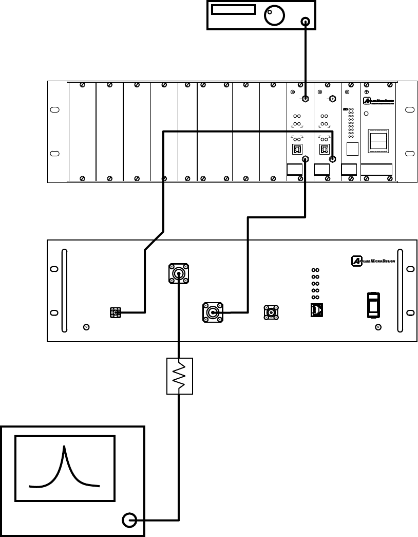
Downlink Test
Shown below is a test set-up of the Downlink chain of the Head End. The signal generator is
set for 478.2500 MHz with a level of -90 dBm. The signal generator output is applied to the
Duplexer Input/Output port of the 1473PA-HE at “ A. “
The RF Output of the DSP is connected to a spectrum analyzer. The expected signal level at
“ B “ is around -30 dBm.
Signal Generator
RF In
Spectrum Analyzer
RF In 478.2500 MHz at -90 dBm
DOWNLINK 478.2500 MHz
Attenuator
LNA
PA
Model No.
1473PA-HE
µP
HD30676
Duplexer
G-Way Microwave
CD479.8/2SK-F3
ZFL-500HLN
DSP-U
DSP-D
Model No.
1456DSP
µP
A
B
RF Output 478.2500 MHz at -30 dBm
14
Power Amplifer/LNA
Model No. 1473PA-HE
Signal Generator
RF In
Spectrum Analyzer
DOWNLINK 478.2500 MHz
ETHERNET
TEMP FLT
STATUS
PA CUR
LNA CUR
FWD PWR
FAN FLT
KEY
REFL PWR
PA CUR FLT
LNA CUR FLT POWER
IN/OUT
RF OUT
400 MHz AMPLIFIER/LNA
MODEL 1473PA
RF IN
AMPLIFIER
DUPLEXER
LNA
SAMPLE
PORT
ETHERNET
W3
W8
W5
W6
W7
W4
W1
W2
FLT
FLT
FLT
FLT
FLT
FLT
PWR
FLT
FLT
RF OUT
RF IN
TX
STATUS
RX
1
1
1
2
2
2
RF OUT
RF IN
TX
STATUS
RX
1
1
1
2
2
2
SUPPLY
POWER
POWER
DSP
Model No. 1456DSP
Downlink Test Set-Up
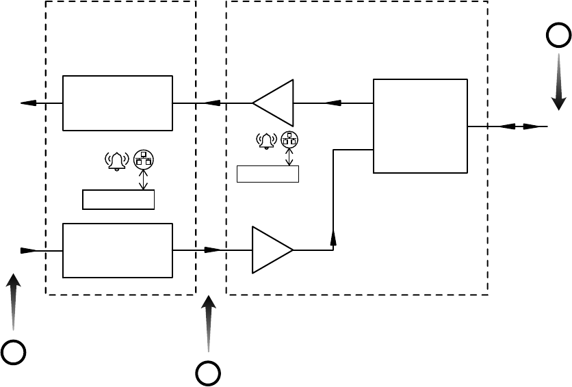
Uplink
15
AB
C
LNA
PA
Model No.
1473PA-HE
µP
HD30676
Duplexer
G-Way Microwave
CD479.8/2SK-F3
ZFL-500HLN
DSP-U
DSP-D
Model No.
1456DSP
µP
The Uplink chain of the Head End consists of a digital signal processor (DSP) card, a Low-
Noise Amplifier (LNA) and a Duplexer. The RF signal is applied to “ A “ shown below at the
DSP RF In port.
The RF signal is fed into the DSP card for filtering and level adjustment to ensure the signal
level is always constant at “ B. “ The signal goes into the power amplifier and is fed into the
Uplink port of the Duplexer. The Duplexer separates the Downlink signals from the Uplink
signals. The signal comes out at “ C. “
The amplifier has an Automatic Level Control (ALC) feature. This feature limits the power
amplifier output in case the input to the amplifier exceeds the required level.
The power amplifier ALC level is set to +30 dBm.
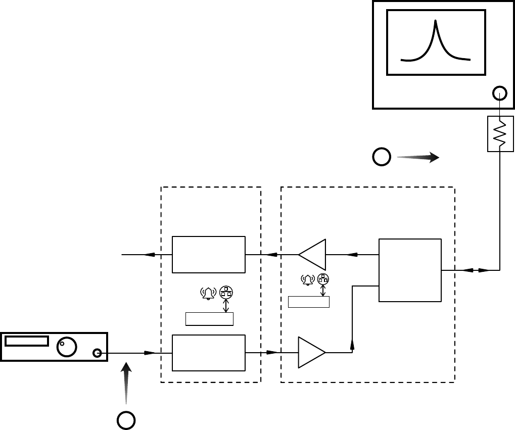
Uplink Test
16
Signal Generator
RF In
Spectrum Analyzer
RF In 481.2500 MHz at -90 dBm
Attenuator
UPLINK 481.2500 MHz
LNA
PA
Model No.
1473PA-HE
µP
HD30676
Duplexer
G-Way Microwave
CD479.8/2SK-F3
ZFL-500HLN
DSP-U
DSP-D
Model No.
1456DSP
µP
A
B
RF Out 481.2500 MHz at +20 dBm
Shown below is a test set-up of the Uplink chain of the Head End. The signal generator is set
for 481.2500 MHz with a level of -90 dBm. The signal generator output is applied to the DSP
Input port at “ A. “
The Duplexer Input/Output port is connected to a spectrum analyzer. The expected signal
level at “ B “ is around +20 dBm.
17
Power Amplifer/LNA
Model No. 1473PA-HE
Signal Generator
RF In
Spectrum Analyzer
UPLINK 481.2500 MHz
ETHERNET
TEMP FLT
STATUS
PA CUR
LNA CUR
FWD PWR
FAN FLT
KEY
REFL PWR
PA CUR FLT
LNA CUR FLT POWER
IN/OUT
RF OUT
400 MHz AMPLIFIER/LNA
MODEL 1473PA
RF IN
AMPLIFIER
DUPLEXER
LNA
SAMPLE
PORT
ETHERNET
W3
W8
W5
W6
W7
W4
W1
W2
FLT
FLT
FLT
FLT
FLT
FLT
PWR
FLT
FLT
RF OUT
RF IN
TX
STATUS
RX
1
1
1
2
2
2
RF OUT
RF IN
TX
STATUS
RX
1
1
1
2
2
2
SUPPLY
POWER
POWER
DSP
Model No. 1456DSP
Uplink Test Set-Up

18
Applied Micro Design Inc.