Arcadyan Technology HT2000W HT2000W wifi module User Manual Front End Module
Arcadyan Technology Corporation HT2000W wifi module Front End Module
Contents
Front-End Module User Manual
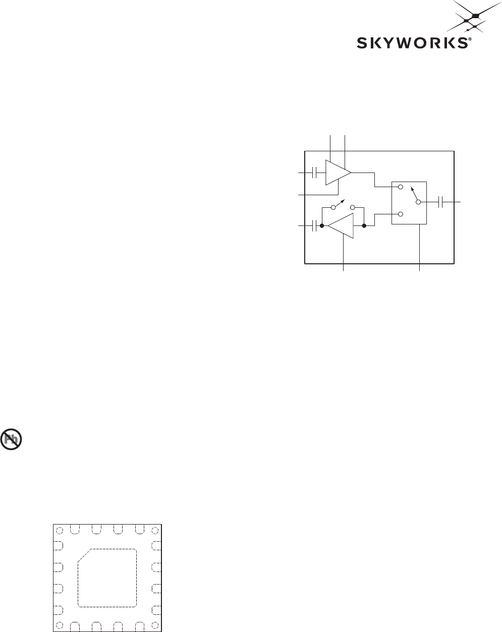
Skyworks Solutions, Inc. • Phone [781] 376-3000 • Fax [781] 376-3100 • sales@skyworksinc.com • www.skyworksinc.com
203068E • Skyworks Proprietary Information • Products and Product Information are Subject to Change Without Notice • August 18, 2014 1
PRELIMINARY DATA SHEET
SKY85717-21: 5 GHz, 802.11ac Front-End Module
4BApplications
802.11ac set-top boxes, networking, and personal computer
systems
PC cards, PCMCIA cards, mini-cards, and half mini-cards
WLAN enabled wireless video systems
0BFeatures
Integrated high performance 5 GHz PA, LNA with bypass, and
SPDT
Fully-matched input and output
Integrated, positive slope power detector
Transmit loopback mode
Transmit gain: 28 dB
Receive gain: 12 dB
Output power: +19.5 dBm, MCS7, HT40
Output power: +18.5 dBm @ 1.8% EVM, MCS9, HT80
High linearity and high efficiency modes
Direct connection to battery with 5 V nominal supply voltage
Small, QFN (16-pin, 2.5 x 2.5 x 0.4 mm) package
(MSL1, 260 C per JEDEC J-STD-020)
Skyworks Pb-free products are compliant with
all applicable legislation. For additional
information, refer to Skyworks Definition of
Lead (Pb)-Free, document number SQ04-0073.
S3513
VDET
PA_EN
GND
TX
LNA_EN
CRX
GND
ANT
GND
RX
GND
VDD
GND
VCC2
VCC1
VLIN
1
2
3
4
12
11
10
9
5678
1615 14 13
Figure 2. SKY85717-21 Pinout – 16-Pin QFN
(Top View)
PA
LNA
S3512
TX
VC1
V
DET ANT
RX
PA_EN
LNA_EN
VLIN
Figure 1. SKY85717-21 Block Diagram
1BDescription
The SKY85717-21 is a highly-integrated, 5 GHz front-end module
(FEM) incorporating a 5 GHz single-pole, double-throw (SPDT)
transmit/receive (T/R) switch, a 5 GHz low-noise amplifier (LNA)
with bypass, and a 5 GHz power amplifier (PA) intended for
mobile/portable 802.11ac applications and systems.
An enable/disable function is included that allows power savings
during off mode. An integrated power detector with 20 dB of
dynamic range is included to provide closed-loop power control
within the system.
The device is provided in a compact, 16-pin 2.5 x 2.5 x 0.4 mm
Quad Flat No-Lead (QFN) package. A functional block diagram is
shown in Figure 1. The pin configuration and package are shown
in Figure 2. Signal pin assignments and functional pin
descriptions are provided in Table 1.

PRELIMINARY DATA SHEET • SKY85717-21: FRONT-END MODULE
Skyworks Solutions, Inc. • Phone [781] 376-3000 • Fax [781] 376-3100 • sales@skyworksinc.com • www.skyworksinc.com
2 August 18, 2014 • Skyworks Proprietary Information • Products and Product Information are Subject to Change Without Notice • 203068E
5BTechnical Description
The SKY85717-21 is comprised of a high performance 5 GHz PA,
5 GHz LNA, and broadband SPDT switch. The device is fully-
matched, and requires few external components for optimal
performance, which makes it ideal for small portable/mobile
applications. The FEM provides up to +28 dB of gain over the
frequency band. The LNA supports an enable/disable mode for
power savings when not in receive mode and a bypass function
for increased receive dynamic range. The PA can be shut off
using the PA_EN signal (pin 6).
2BElectrical and Mechanical Specifications
Signal pin assignments and functional pin descriptions are
described in Table 1. The absolute maximum ratings of the
SKY85717-21 are provided in Table 2. The recommended
operating conditions are specified in Table 3 and electrical
specifications are provided in Tables 4, 5, and 6.
The state of the SKY85717-21 is determined by the logic provided
in Table 7.
6BPackage and Handling Information
Instructions on the shipping container label regarding exposure to
moisture after the container seal is broken must be followed.
Otherwise, problems related to moisture absorption may occur
when the part is subjected to high temperature during solder
assembly.
The SKY85717-21 is rated to Moisture Sensitivity Level 1 (MSL1)
at 260 C. It can be used for lead or lead-free soldering. For
additional information, refer to the Skyworks Application Note,
Solder Reflow Information, document number 200164.
Care must be taken when attaching this product, whether it is
done manually or in a production solder reflow environment.
Production quantities of this product are shipped in a standard
tape and reel format.
Table 1. SKY85717-21 Signal Descriptions
Pin Name Description Pin Name Description
1 GND Ground 9 VLIN Transmit linearity mode control
2 RX RF receive output 10 VCC1 Supply voltage
3 GND Ground 11 VCC2 Supply voltage
4 VDD LNA supply voltage and transmit bias 12 GND Ground
5 VDET Detector output voltage 13 ANT Antenna
6 PA_EN PA enable 14 GND Ground
7 GND Ground 15 CRX Switch control voltage
8 TX RF transmit input 16 LNA_EN LNA enable
Note: N/C = No connect. Keep pin floating.

PRELIMINARY DATA SHEET • SKY85717-21: FRONT-END MODULE
Skyworks Solutions, Inc. • Phone [781] 376-3000 • Fax [781] 376-3100 • sales@skyworksinc.com • www.skyworksinc.com
203068E • Skyworks Proprietary Information • Products and Product Information are Subject to Change Without Notice • August 18, 2014 3
Table 2. SKY85717-21 Absolute Maximum Ratings (Note 1)
Parameter Symbol Minimum Maximum Units
Supply voltage (non-operating, no RF) VCC
VDD
–1
–1
+6
+6
V
V
DC input on control pin (PA_EN, LNA_EN,
CRX, VLIN)
VIN –0.3
+6.0
V
Input power (ANT terminated in 50 Ω match) PIN
+5
dBm
Case operating temperature TA –40 +85 C
Storage temperature TST –40 +140 C
Electrostatic discharge:
Human Body Model (HBM), Class 1C
ESD
1000
V
Note 1: Exposure to maximum rating conditions for extended periods may reduce device reliability. There is no damage to device with only one parameter set at the limit and all other
parameters set at or below their nominal value. Exceeding any of the limits listed here may result in permanent damage to the device.
CAUTION: Although this device is designed to be as robust as possible, electrostatic discharge (ESD) can damage this device. This device
must be protected at all times from ESD. Static charges may easily produce potentials of several kilovolts on the human body
or equipment, which can discharge without detection. Industry-standard ESD precautions should be used at all times.
Table 3. SKY85717-21 Recommended Operating Conditions
Parameter Symbol Minimum Typical Maximum Units
Supply voltage relative to GND = 0 V VCC, VDD 3.9 5.0 5.5 V
Operating temperature TA –40 +25 +85 C
Table 4. SKY85717-21 Electrical Specifications: DC Characteristics (Note 1)
(VCC = 5.0 V, PA_EN = 3.3 V, TA = 25 °C, All Unused Ports Terminated with 50 Ω, Unless Otherwise Noted)
Parameter Symbol Test Condition Min Typical Max Units
Supply current, high linearity mode ICC-A POUT = +20.5 dBm, VLIN = 3.3 V 230 260 mA
Supply current, high efficiency mode ICC-A POUT = +20.5 dBm, VLIN = 0 V 220 240 mA
Supply current ICC-OFF No RF applied, PA_EN = CRX =
LNA_EN = 0 V
20
μA
Quiescent current, high efficiency mode ICQ No RF 170 mA
LNA supply current ICC_LNA LNA_EN = 3.3 V, CRX = 3.3 V 11 mA
LNA bypass supply current ICC_LNA_BYP LNA_EN = 0 V, CRX = 3.3 V 200 μA
TNote 1: Performance is guaranteed only under the conditions listed in this table.

PRELIMINARY DATA SHEET • SKY85717-21: FRONT-END MODULE
Skyworks Solutions, Inc. • Phone [781] 376-3000 • Fax [781] 376-3100 • sales@skyworksinc.com • www.skyworksinc.com
4 August 18, 2014 • Skyworks Proprietary Information • Products and Product Information are Subject to Change Without Notice • 203068E
Table 5. SKY85717-21 Electrical Specifications: General (Note 1)
(VCC = 5.0 V, PA_EN = 3.3 V, LNA_EN = CRX = 0 V, TA = 25 °C, All Unused Ports Terminated with 50 Ω, Unless Otherwise Noted)
Parameter Symbol Test Condition Min Typical Max Units
Transmit Characteristics
Frequency range f 4900 5850 MHz
Error Vector Magnitude, high linearity
mode
EVM 5150 to 5850 MHz, VLIN = 3.3 V:
POUT = +19.5 dBm, MCS7, HT40
POUT = +18.5 dBm, MCS9, HT80
1.8
3.0
2.0
%
%
Error Vector Magnitude, high efficiency
mode
EVM 5150 to 5850 MHz, VLIN = 0 V:
POUT = +19.5 dBm, MCS7, HT40
POUT = +18.5 dBm, MCS9, HT80
1.8
3.0
2.0
%
%
Output power POUT MCS0, mask compliance +22 +24 dBm
Small signal gain S21 5150 to 5850 MHz 28 dB
Harmonics (2nd and 3rd) 2fo, 3fo POUT = +20 dBm, 6 Mbps, 802.11a –45 dBm/MHz
Delay and rise/fall time tDR, tDF 50% of VPA_EN edge and 90/10% of
final output power level
400
ns
Input return loss S11 @ TX port –12 dB
Stability Stab 802.11n, MCS0, HT40, POUT =
+20 dBm, 0.1 GHz to 20 GHz, load
VSWR = 6:1
All non-harmonically related outputs < –43 dBm/MHz
Ruggedness CW, PIN = 0 dBm, 0.1 GHz to
20 GHz, load VSWR = 10:1 No permanent damage or performance degradation
Receive Characteristics
Frequency range f 4900 5850 MHz
Small signal gain S21 LNA enabled
Bypass mode
+12
–8
dB
dB
Noise figure NF 2.5 dB
3P
rd
P Order Input Intercept Point IIP3 LNA enabled
Bypass mode
+5
+20
dBm
dBm
Input return loss S11 LNA enabled
Bypass mode
–8
–8
dB
dB
Output return loss S22 –8 dB
Enable time tEN 10% to 90% of receive RF power,
from time that LNA_EN is at 50%
400
ns
Power Detector Characteristics
Frequency range f 4900 5850 MHz
Power detector range, CW PDR Measured @ ANT pin 0 +23 dBm
Output impedance PDZLOAD 2.2 kΩ
Output voltage PDVNO_RF
PDVP21
POUT = no RF, measured into 1
MΩ
POUT = +21 dBm, CW, measured
into 1 MΩ
0.2
0.9
V
V
Detector bandwidth PDBW 3.6 MHz
TNote 1: Performance is guaranteed only under the conditions listed in this table.

PRELIMINARY DATA SHEET • SKY85717-21: FRONT-END MODULE
Skyworks Solutions, Inc. • Phone [781] 376-3000 • Fax [781] 376-3100 • sales@skyworksinc.com • www.skyworksinc.com
203068E • Skyworks Proprietary Information • Products and Product Information are Subject to Change Without Notice • August 18, 2014 5
Table 6. SKY85717-21 Electrical Specifications: Control Logic Characteristics (Note 1)
(VCC = 5.0 V, PA_EN = 3.3 V, LNA_EN = CRX = 0 V, TA = 25 °C, All Unused Ports Terminated with 50 Ω, Unless Otherwise Noted)
Parameter Symbol Test Condition Min Typical Max Units
Control voltage:
High
Low
VIH
VIL
1.6
0
3.6
0.4
V
V
Input current, high IIH 120 μA
Input current, low IIL 1 μA
TNote 1: Performance is guaranteed only under the conditions listed in this table.
Table 7. SKY85717-21 Control Logic
Mode CRX (Pin 15) LNA_EN (Pin 16)
(Note 1)
PA_EN (Pin 6)
(Note 2)
VLIN (Pin 9)
WLAN receive 1 1 0 0
WLAN receive bypass mode 1 0 0 0
WLAN transmit, high linearity mode 0 0 1 1
WLAN transmit, high efficiency mode 0 0 1 0
WLAN off 0 0 0 0
N
ote 1: LNA is on while LNA_EN is high. LNA is off and in bypass mode when LNA_EN is low.
N
ote 2: PA_EN controls PA enable and transmit/receive switch logic.
PRELIMINARY DATA SHEET • SKY85717-21: FRONT-END MODULE
Skyworks Solutions, Inc. • Phone [781] 376-3000 • Fax [781] 376-3100 • sales@skyworksinc.com • www.skyworksinc.com
6 August 18, 2014 • Skyworks Proprietary Information • Products and Product Information are Subject to Change Without Notice • 203068E
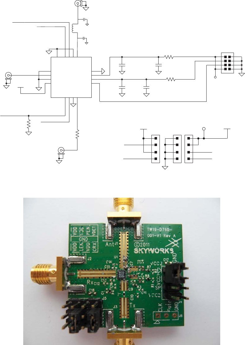
Evaluation Board Description
The SKY85717-21 Evaluation Board is used to test the
performance of the SKY85717-21 FEM. A suggested application
schematic diagram is shown in Figure 3. A photograph of the
Evaluation Board is shown in Figure 4. A Bill of Materials (BOM)
for the Evaluation Board is provided in Table 8.
Evaluation Board Test Procedures
1. Connect the system ground to connector J4, pin 2, of the
Evaluation Board.
2. Apply 5 V to connector J4, pins 1 and 3.
3. Select a path to test according to the modes shown in
Table 7.
4. Connect a multimeter or oscilloscope to connector J5, pin 12,
to monitor the power detector voltage.
5. Apply an RF signal to connector J1 (ANT) to monitor the RX to
ANT performance. Measure the response from the output of
connector J2 (RX).
6. Apply an RF signal to connector J3 (TX) to monitor the ANT to
TX performance. Monitor the output power on connector J1
(ANT). Care should be taken not to overdrive the amplifier by
applying too much RF on the input to the device (–20 dBm
provides a suitable starting input power for the device).
9BCircuit Design Considerations
The following design considerations are general in nature and
must be followed regardless of final use or configuration:
Paths to ground should be made as short as possible.
The RX and ANT ports are AC-coupled and do not require DC
blocking capacitors. There are ESD diodes to ground and a DC
blocking capacitor between the TX port (pin 8) and the die.
Therefore, there is no DC present on this port.
If the TX port is connected to an external component with
>3 VDC present on it, a 10 pF (component C8) general
purpose blocking capacitor is recommended.
Capacitors C6 (1 μF) and C7 (100 pF) should be on the
primary side of the Evaluation Board at a minimum
manufacturable distance from the FEM.
Capacitor C20 (0.3 pF) needs to be as close as possible at
manufacturable distance from the ANT pin of the IC, followed
by L1 (1.0 nH) and C19 (0.3 pF), also at manufacturable
distance from C20 and L1, respectively.
The ground pad of the SKY85717-21 has special electrical
and thermal grounding requirements. This pad is the main
thermal conduit for heat dissipation. Because the circuit board
acts as the heat sink, it must shunt as much heat as possible
from the device. Therefore, design the connection to the
ground pad to dissipate the maximum wattage produced by
the circuit board. Multiple vias to the grounding layer are
required.
Evaluation Board trace losses are:
RX = TX = 0.32 dB and ANT = 0.35 dB.
NOTE: A poor connection between the ground pad and the
ground increases the junction temperature (TJ), which
reduces the life of the device.
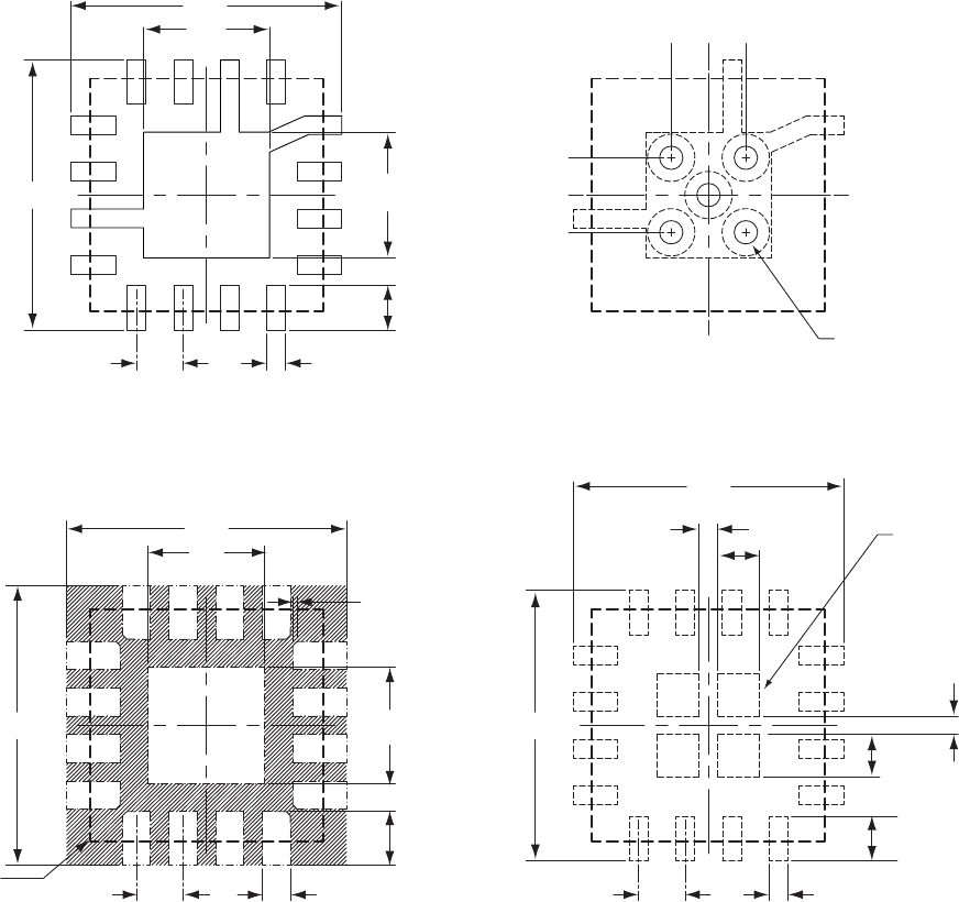
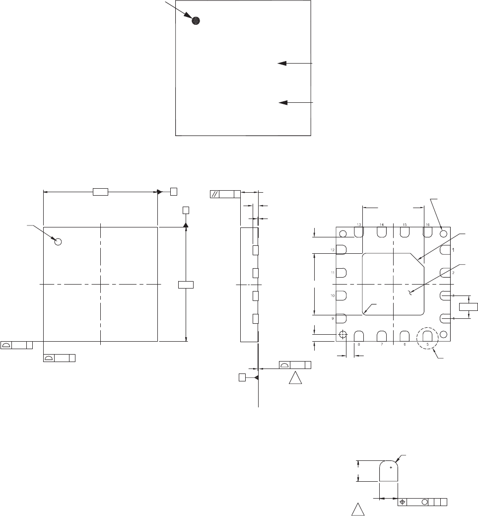
Package Dimensions
The PCB layout footprint for the SKY85717-21 is shown in
Figure 5. Typical part markings are shown in Figure 6. Package
dimensions for the 16-pin QFN are shown in Figure 7, and tape
and reel dimensions are provided in Figure 8.
PRELIMINARY DATA SHEET • SKY85717-21: FRONT-END MODULE
Skyworks Solutions, Inc. • Phone [781] 376-3000 • Fax [781] 376-3100 • sales@skyworksinc.com • www.skyworksinc.com
203068E • Skyworks Proprietary Information • Products and Product Information are Subject to Change Without Notice • August 18, 2014 7
VDD
LEN
CRX
TP2
J5
4
1
J5 J5
7
10
5
2
8
11
6
3
9
12
VDD
PEN
VDET
1GND
RX
GND
VDD
VDET
PA_EN
GND
TX
LNA_EN
CRX
GND
ANT
GND
VCC2
VCC1
VLIN
2
3
4
12
11
10
9
5678
1615 14 13
C8
0 Ω
C7
100 pF
C6
1 μF
C3
1 μF
25 Ω
R8
0 Ω
R7 VCC2
VCC1
TP1
C4
1 μF
5
2
8
1
6
3
7
4
1
J4
PAD
17
LEN
CRX
VDD
PEN
R4
26.1 K
VDET
SMA
J1
SMA
J2
SMA
J3
Y0585
L1
1.0 nH C20
0.3 pF
C19
0.3 pF
Figure 3. SKY85717-21 Application Schematic
Y0461
Figure 4. SKY85717-21 Evaluation Board Assembly

PRELIMINARY DATA SHEET • SKY85717-21: FRONT-END MODULE
Skyworks Solutions, Inc. • Phone [781] 376-3000 • Fax [781] 376-3100 • sales@skyworksinc.com • www.skyworksinc.com
8 August 18, 2014 • Skyworks Proprietary Information • Products and Product Information are Subject to Change Without Notice • 203068E
Table 8. SKY85717-21 Evaluation Board Bill of Materials (BOM)
Reference Value Manufacturer Mfr Part Number Package Description
R7 0 Ω Panasonic ERJ2GEJ0R0 0402 Thick film chip resistor
L1 1.0 nH Murata LQG15HN1N0S02D 0402 High frequency multilayer
R8 24.9 Ω Panasonic ERJ2RKF24R9 0402 Thick film chip resistor
R4 26.1K Panasonic ERJ2RKF2612 0402 Thick film chip resistor
C7 100 pF Murata GRM1555C1H101JZ01 0402 Multilayer ceramic
C19, C20 0.3 pF Murata GJM1555C1HR30WB01 0402 RF, High Q, low loss
C8, R3 0 Ω Panasonic ERJ2GE0R00 0402 Thick film chip resistor
C3, C4, C6 1 uF TDK Corporation C1005X5R1A105K 0402 Multilayer ceramic
PRELIMINARY DATA SHEET • SKY85717-21: FRONT-END MODULE
Skyworks Solutions, Inc. • Phone [781] 376-3000 • Fax [781] 376-3100 • sales@skyworksinc.com • www.skyworksinc.com
203068E • Skyworks Proprietary Information • Products and Product Information are Subject to Change Without Notice • August 18, 2014 9
2.90
2X 0.40
5X ø0.250
2X 0.40
2X 0.40
00
2X 0.40
00
2.90
0.20 Typ.
0.20 Typ.
0.45 Typ.
0.45 Typ.
Via Pattern
(Note 4)
Board Metal
Solder Mask Pattern
(Note 6)
Stencil Pattern
(Note 5)
S2655
Notes:
1. All dimensions are in millimeters
2. Dimensioning and tolerancing according to ASME Y14.5M-1994
3. Unless specified, dimensions are symmetrical about center lines.
4. Via hole recommendations: 0.025 mm Cu via wall plating (minimum),
soldermask on the far side should tent or plug via holes.
5. Stencil recommendations: 0.10 mm stencil thickness, laser cut
apertures, trapezoidal walls and rounded corners offer better paste release.
6. Solder mask recommendations: contact board fabricator for recommended
solder mask offset and tolerance.
3.00
3.00 2.90
1.25
2.90
1.35
1.25
1.35
0.475 Typ.
0.20 Typ.0.500 Typ.
0.475 Typ.
0.575 Typ.
0.30 Typ.
8X
C0.050 X 45°
0.20 Typ.0.500 Typ.
0.500 Typ.
13141516
1
2
3
4
12
14
12
11
10
9
567
3
8
13141516
1
2
3
4
12
11
10
9
5678
13141516
1
2
3
4
12
11
10
9
5678
52% solder coverage
on center pad
Package
Outline
Figure 5. SKY85717-21 PCB Layout Footprint
PRELIMINARY DATA SHEET • SKY85717-21: FRONT-END MODULE
Skyworks Solutions, Inc. • Phone [781] 376-3000 • Fax [781] 376-3100 • sales@skyworksinc.com • www.skyworksinc.com
10 August 18, 2014 • Skyworks Proprietary Information • Products and Product Information are Subject to Change Without Notice • 203068E
SKY21
85717
XXXXX
Pin1
Indicator
Skyworks
Part Number
Lot Number
Y0460
Figure 6. Typical Part Markings
(Top View)
Top View Side View Bottom View
See Detail A
2.50 0.40 Max
Exposed Pad
1.35 ± 0.05
0.225 ± 0.05
16X 0.30 Min
8X 0.12 Min
4X ø0.15, Internal
Support Only. Do Not
Solder or Route Under
Notes:
1. All measurements are in millimeters.
2. Dimensions and tolerances according to ASME Y14.5M-1994.
3. Unless otherwise specified the following values apply:
Decimal Tolerance: Angular Tolerance:
X.X (1 place)
± 0.1 mm ± 0.5°
X.XX (2 places) ± 0.05 mm
X.XXX (3 places) ± 0.025 mm
4. Coplanarity applies to the terminals as well as all other bottom
surface metallization.
5. Dimension applies to metallized terminal. If terminal tip has a
radius, dimension should not be measured in that radius area.
6. Unless specified, dimensions are symmetrical about center lines.
2.50
Pin 1
Indicator
0.05 C
0.05 C
2X
2X
2X 0.075
0.10 M C A B
A
B
0.20 ± 0.05
5
4
0.500
0.05 C
Pin 1
Indicator
O.30 x 45°
8X 0.15
C
Seating
Plane
1.35 ± 0.05
0.127 Ref
0.02 + 0.03
–0.02
0.05 C21X
R0.075, Typ
Detail A
Scale 2X
16 Places
Y1253
Figure 7. SKY85717-21 16-Pin QFN Package Dimensions

PRELIMINARY DATA SHEET • SKY85717-21: FRONT-END MODULE
Skyworks Solutions, Inc. • Phone [781] 376-3000 • Fax [781] 376-3100 • sales@skyworksinc.com • www.skyworksinc.com
203068E • Skyworks Proprietary Information • Products and Product Information are Subject to Change Without Notice • August 18, 2014 11
S2678a
2.00 ± 0.05)
(See Note 1)
4.00 ± 0.1
(See Note 2)
2.75 ± 0.05
4.00 ± 0.10
∅1.55 ± 0.05
∅1.00 Min.
8.00 + 0.30/– 0.10
3.50 ± 0.10
(See Note 1)
2.75 ± 0.05
1.75 ± 0.1
Pin 1
Indicator
0.25 ± 0.05
0.70 ± 0.10
A
A
A
R0.1 Typ.
Notes:
1. Measured from centerline of sprocket hole to centerline of pocket.
2. Cumulative tolerance of 10 sprocket holes: ±0.02 mm.
3. All measurements are in millimeters.
C
L
Figure 8. SKY85717-21 Tape and Reel Dimensions

PRELIMINARY DATA SHEET • SKY85717-21: FRONT-END MODULE
Skyworks Solutions, Inc. • Phone [781] 376-3000 • Fax [781] 376-3100 • sales@skyworksinc.com • www.skyworksinc.com
12 August 18, 2014 • Skyworks Proprietary Information • Products and Product Information are Subject to Change Without Notice • 203068E
8BOrdering Information
Model Name Manufacturing Part Number Evaluation Board Part Number
SKY85717-21: 5 GHz, 802.11ac Front-End Module SKY85717-21 SKY85717-21-EVB
Copyright © 2014 Skyworks Solutions, Inc. All Rights Reserved.
Information in this document is provided in connection with Skyworks Solutions, Inc. (“Skyworks”) products or services. These materials, including the information contained herein, are provided by
Skyworks as a service to its customers and may be used for informational purposes only by the customer. Skyworks assumes no responsibility for errors or omissions in these materials or the
information contained herein. Skyworks may change its documentation, products, services, specifications or product descriptions at any time, without notice. Skyworks makes no commitment to
update the materials or information and shall have no responsibility whatsoever for conflicts, incompatibilities, or other difficulties arising from any future changes.
No license, whether express, implied, by estoppel or otherwise, is granted to any intellectual property rights by this document. Skyworks assumes no liability for any materials, products or
information provided hereunder, including the sale, distribution, reproduction or use of Skyworks products, information or materials, except as may be provided in Skyworks Terms and Conditions
of Sale.
THE MATERIALS, PRODUCTS AND INFORMATION ARE PROVIDED “AS IS” WITHOUT WARRANTY OF ANY KIND, WHETHER EXPRESS, IMPLIED, STATUTORY, OR OTHERWISE, INCLUDING FITNESS FOR A
PARTICULAR PURPOSE OR USE, MERCHANTABILITY, PERFORMANCE, QUALITY OR NON-INFRINGEMENT OF ANY INTELLECTUAL PROPERTY RIGHT; ALL SUCH WARRANTIES ARE HEREBY EXPRESSLY
DISCLAIMED. SKYWORKS DOES NOT WARRANT THE ACCURACY OR COMPLETENESS OF THE INFORMATION, TEXT, GRAPHICS OR OTHER ITEMS CONTAINED WITHIN THESE MATERIALS. SKYWORKS
SHALL NOT BE LIABLE FOR ANY DAMAGES, INCLUDING BUT NOT LIMITED TO ANY SPECIAL, INDIRECT, INCIDENTAL, STATUTORY, OR CONSEQUENTIAL DAMAGES, INCLUDING WITHOUT LIMITATION,
LOST REVENUES OR LOST PROFITS THAT MAY RESULT FROM THE USE OF THE MATERIALS OR INFORMATION, WHETHER OR NOT THE RECIPIENT OF MATERIALS HAS BEEN ADVISED OF THE
POSSIBILITY OF SUCH DAMAGE.
Skyworks products are not intended for use in medical, lifesaving or life-sustaining applications, or other equipment in which the failure of the Skyworks products could lead to personal injury,
death, physical or environmental damage. Skyworks customers using or selling Skyworks products for use in such applications do so at their own risk and agree to fully indemnify Skyworks for any
damages resulting from such improper use or sale.
Customers are responsible for their products and applications using Skyworks products, which may deviate from published specifications as a result of design defects, errors, or operation of
products outside of published parameters or design specifications. Customers should include design and operating safeguards to minimize these and other risks. Skyworks assumes no liability for
applications assistance, customer product design, or damage to any equipment resulting from the use of Skyworks products outside of stated published specifications or parameters.
Skyworks and the Skyworks symbol are trademarks or registered trademarks of Skyworks Solutions, Inc., in the United States and other countries. Third-party brands and names are for
identification purposes only, and are the property of their respective owners. Additional information, including relevant terms and conditions, posted at www.skyworksinc.com, are incorporated by
reference.