Asia Pacific Satellite communications SM-2500 Thuraya Satellite Module User Manual
Asia Pacific Satellite communications Inc. Thuraya Satellite Module
User Manuel

THURAYA Second-Generation User Terminal
SM-2500 Technical Information Manual
Document No.: AP01-601-08
Asia Pacific Satellite Industries Co., Ltd
9FL, IT Castle 2-Dong, #550-1, Gasan-Dong, GeumCheon-Gu,
Seoul, Korea
Copyright © 2006 Asia Pacific Satellite Industries Co., Ltd
All Rights Reserved
APSI Proprietary
All information contained in or disclosed by this document is confidential and proprietary to APSI.
By accepting this material the recipient agrees that this material and the information contained
therein will be held in confidence and will not be reproduced in whole or in part without express
written permission from APSI.

THURAYA Second-Generation User Terminal
SM-2500 Technical Information Manual
Document No.: AP01-601-08
+Update: 02/11/06 Ver: 0.8 Page 2 of 21
This page contains confidential information, which is protected by copyright and is proprietary to APSI.
No part of this document may be used, copied, disclosed or conveyed to another party without prior written consent of APSI
CONTENTS
1 INTRODUCTION ...................................................................................................... 3
2 PIN DESCRIPTION .................................................................................................. 5
3 POWER SUPPLY..................................................................................................... 8
4 CONTROL SIGNALS............................................................................................. 12
5 RTC BACKUP BATTERY INTERFACE................................................................. 13
6 UART INTERFACE ................................................................................................ 13
7 USB INTERFACE................................................................................................... 14
8 AUDIO INTERFACE............................................................................................... 14
9 SIM CARD INTERFACE ........................................................................................ 14
10 LCD INTERFACE................................................................................................... 15
11 BACKLIGHT INTERFACE..................................................................................... 15
12 KEYPAD INTERFACE ........................................................................................... 15
17 MECHANICAL INTERFACE.................................................................................. 16
18 HEAT DISSIPATION.............................................................................................. 18
THURAYA Second-Generation User Terminal
SM-2500 Technical Information Manual
Document No.: AP01-601-08
+Update: 02/11/06 Ver: 0.8 Page 3 of 21
This page contains confidential information, which is protected by copyright and is proprietary to APSI.
No part of this document may be used, copied, disclosed or conveyed to another party without prior written consent of APSI
1 Introduction
1.1 Scope
The purpose of this document is to explain the hardware technical information and
specifications of SM-2500, Thuraya satellite module. This document will be helpful to
third party designers and manufactuers.
For the AT command set of SM-2500, It will be dealt with another document. Please refere to
the document number AP01-344-49,Thuraya Second Generation User Terminal AT Command
Set.
1.2 Related documents
Table 1 Related documents
Document Number Remark
AP01-344-49 Thuraya Second Generation User Terminal AT Command Set
ETSI TS 101 376-5-5 GMR-1 05.05, and GMPRS-1 05.05
Radio Transmission and Reception.
1.3 Terms and abbreviations
Table 2 Terms and abbreviatioins
Abbreviation Description
SAT Satellite.
GPS Global Positioning System
PA Power Amplifier
GMR GEO Mobile Radio
RF Radio Frequency
UART Universal Asynchronous Receive and Transmitt
RTC Real Time Clock
THURAYA Second-Generation User Terminal
SM-2500 Technical Information Manual
Document No.: AP01-601-08
+Update: 02/11/06 Ver: 0.8 Page 4 of 21
This page contains confidential information, which is protected by copyright and is proprietary to APSI.
No part of this document may be used, copied, disclosed or conveyed to another party without prior written consent of APSI
1.4 Overview
The Thuraya SM-2500 is a stand alone device which is able to access satellite mobile
services via the GMR-1 and GMPRS-1 air interface, without additional components
apart from the following: SAT antenna, GPS antenna, keypad, LCD, GSM Module,
Bluetooth Module and battery / power supply.
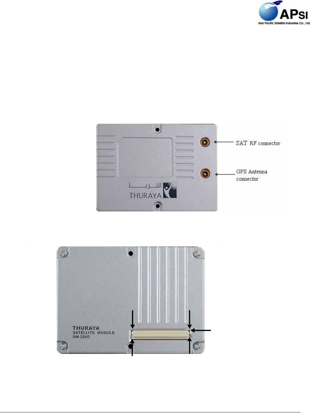
The following Figure1 and Figure 2 shows the outline of SM-2500 and external
interfaces that sat antenna RF connector, GPS antenna connector and 100 pins of
board to board connector.
Figure 1 Top side
Figure 2 Bottom side
Pin 2 Pin 100
B to B
connector
Pin 1 …Pin 99

THURAYA Second-Generation User Terminal
SM-2500 Technical Information Manual
Document No.: AP01-601-08
+Update: 02/11/06 Ver: 0.8 Page 5 of 21
This page contains confidential information, which is protected by copyright and is proprietary to APSI.
No part of this document may be used, copied, disclosed or conveyed to another party without prior written consent of APSI
2 Pin description
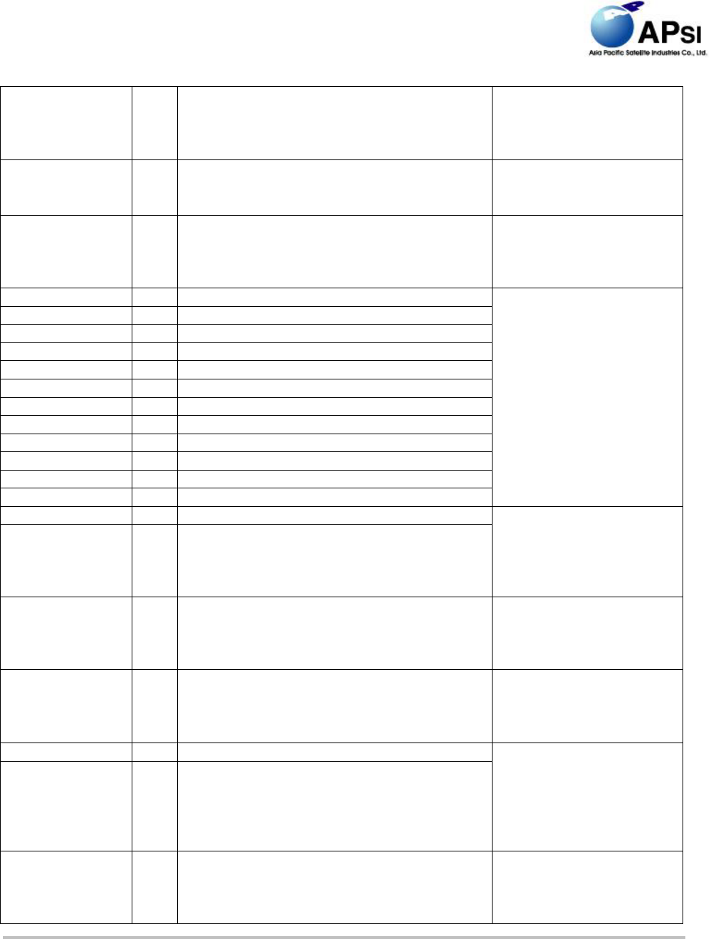
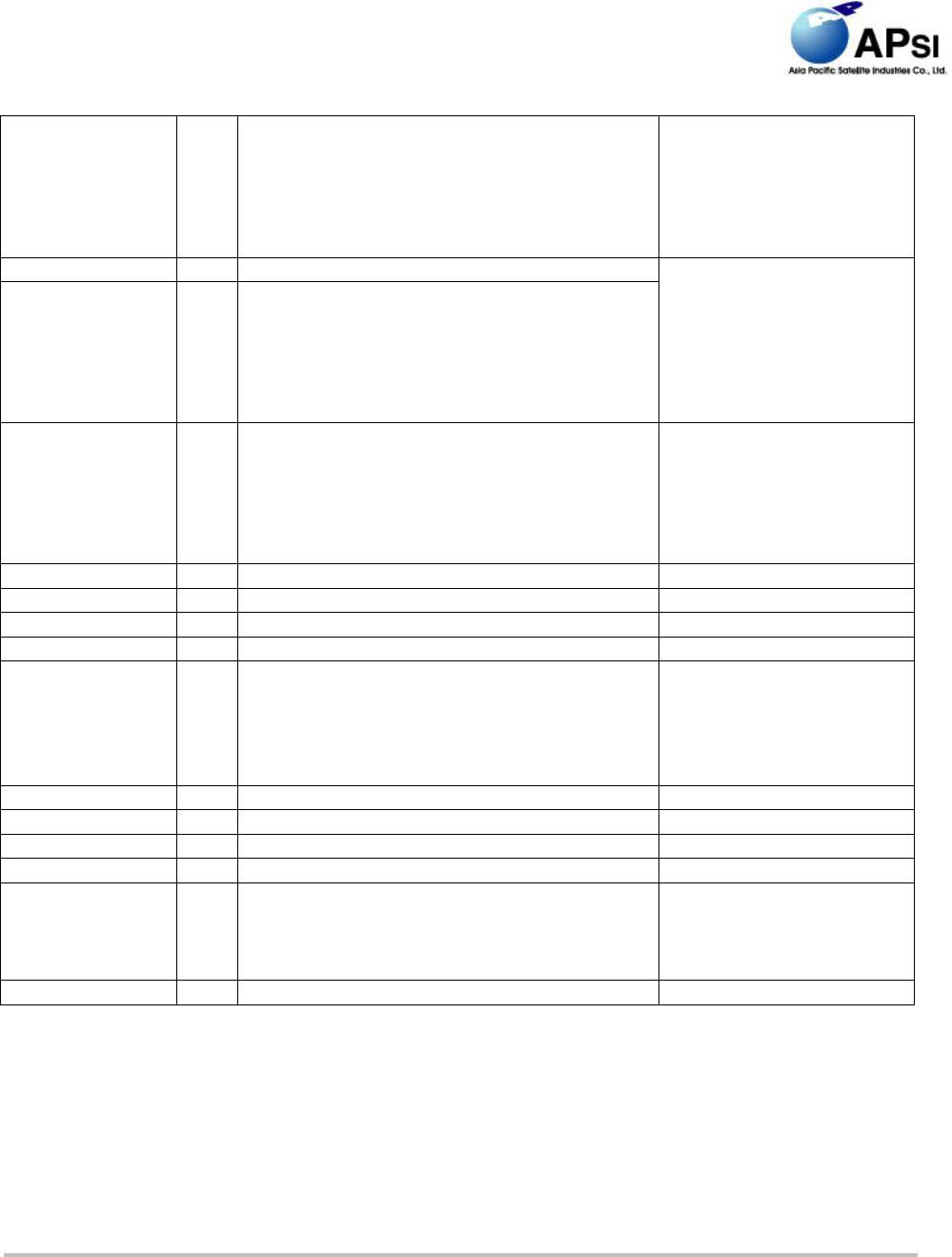
SAT module has 100-pins B-to-B connector for interface with external device. Each pin, its designated
function and interface is shown in Table 3 below.
Table 3 Pin functional and electrical description
PIN NAME I/O DESCRIPTION ELECTRICAL SPEC.
VPWR I 6 pin-allotted VPWR at board-to-board of SAT
Module use as power and allowed input power is
+3.2~4.5V.
Supply max current: 300 ㎃ (at 3.7, VEXT not
used)
VImax = +4.5V
VImin = +3.2V
VItyp = +3.7V
5V_TX I Pin-allotted 5V_TX at board-to-board of SAT
Module use as input power of RF power
amplifier and allowed input power is
+4.8V~5.3V.
This power has to be low ripple noise and enable
to supply 1.5A (at 5V) of peak voltage well
when TX transmit burst.
VImax = +5.3 V
VImin = +4.8V
VItyp = +5.0V
VEXT O Power to supply external 3V. User can power off
the module to prevent malfunction of module
when this power exceed of allowed range.
Prohibit approving external load of above
200 ㎃.
VOmax = +3.1V
VOmin = +2.9V
VOtyp = +3.0V
IOLmax = 200 ㎃
LCD_D[0:7] I/O 8bit bi-directional data bus for LCD data
/LCD_CS O LCD chip select output pin. Data/Iinstruction is
enabled only when LCD_CS is low level.
/LCD_RD O Servers as a read strobe signal and read data at
the low level.
/LCD_WR O Servers as a write strobe signal and write data at
the low level.
LCD_RS O Data/Instruction select output pin
H:LCD_D[0:7] are display data
L: LCD_D[0:7] are instruction data
VOHmin = 2.4V
VOLmax = 0.6V
IOL = 4 ㎃
VIHmin = 2.1V
VILmax = 0.9V
IIL = 1 ㎂
LCD_EN O External LCD part power enable output pin.
Active high
/LCD_RESET O LCD reset output pin.
When /LCD_RESET is low level, initialization
is executed.
LCD_BL_EN O White LED to backlight of LCD module enable
pin. Active high
VOHmin = 2.5V
VOLmax = 0.8V
IOL = 8 ㎃
LCD_DIM O White LCD to backlight of LCD module
dimming control pin.
VOHmin = 2.4V
VOLmax = 0.6V
IOL = 4 ㎃
THURAYA Second-Generation User Terminal
SM-2500 Technical Information Manual
Document No.: AP01-601-08
+Update: 02/11/06 Ver: 0.8 Page 6 of 21
This page contains confidential information, which is protected by copyright and is proprietary to APSI.
No part of this document may be used, copied, disclosed or conveyed to another party without prior written consent of APSI
KBR[00:04] I Row line input pin of keypad matrix. VIHmin = 2.1V
VILmax = 0.9V
IIL = 1 ㎂
KBC[00:04] O Column line input pin of keypad matrix. VOHmin = 2.4V
VOLmax = 0.6V
IOL = 4 ㎃
KEYPAD_BL_EN O Keypad backlight enable output pin. Active high VOHmin = 2.5V
VOLmax = 0.8V
IOL = 8 ㎃
UART1_TXD O UART1 serial data output
UART1_RXD I UART1 serial data input.
UART1_CTS I UART1 clear to send input.
UART1_RTS O UART1 request to send output.
UART1_DTR O UART1 data transmit ready output.
UART1_DSR I UART1 data set ready input.
UART1_DCD O UART1 data carrier detect output
UART1_RI O UART1 ring indicator output.
UART2_TXD O UART2 serial data output.
UART2_RXD I UART2 serial data input.
UART2_RTS O UART2 request to send output.
UART2_CTS I UART2 clear to send input.
See table 5 and table 6
I2C_SCL O I2C serial clock output.
I2C_SDA I/O I2C serial bi-directional data.
VIHmin = 2.1V
VILmax = 0.9V
VOLmax = 0.4V
IOL = 3 ㎃
/I2C_INT I External I2C device detect and interrupt input. VIHmin = 2.1V
VILmax = 0.9V
IIL = 20 ㎂
USB_VBUS I USB device detection input. VIHmin = 3.0V
VILmax = 0.5V
IIL = 10 ㎂
USB_DP I/O USB data plus
USB_DM I/O USB data minus
VIHmin = 2.1V
VILmax = 0.75V
VOHmin = 2.0V
VOLmax = 0.8V
IOL = 18.3 ㎃
GM_ON I Input pin to power SAT module on VIHmin = 2.5V
VILmax = 0.5V
IIL = 10 ㎂

THURAYA Second-Generation User Terminal
SM-2500 Technical Information Manual
Document No.: AP01-601-08
+Update: 02/11/06 Ver: 0.8 Page 7 of 21
This page contains confidential information, which is protected by copyright and is proprietary to APSI.
No part of this document may be used, copied, disclosed or conveyed to another party without prior written consent of APSI
GM_OFF I Input pin that to power off the SAT module. VIHmin = 2.1V
VILmax = 0.75V
IIL = 2 ㎃
/GM_RESET I Input pin to initialize SAT module.
When boot up of SAT module, reset signal is
generated by internal circuit to fit the processor
reset timing, so it doesn’t need to generate at
external circuit.
This pin has been pull-up 20 ㏀ resistor.
Thus, float if unused.
VIHmin = 2.1V
VILmax = 0.75V
Id = 20 ㎃
GM_STATUS O Output pin to inform a condition of SAT module
to HOST.
VOHmin = 2.5V
VOLmax = 0.8V
IOL = 8 ㎃
GM_WAKEUP I Input pin to wake SAT module up of sleep
condition.
VIHmin = 2.1V
VILmax = 0.9V
IIL = 20 ㎂
HOST_WAKEUP O Output pin to wake SAT module up before
sending data to HOST when HOST device is in
sleep condition.
VOHmin = 2.4V
VOLmax = 0.6V
IOL = 4 ㎃
GPIO1 I/O General purpose I/O 1.
User can control at command of user’s own
accord.
GPIO2 I/O General purpose I/O 2.
User can control at command of user’s own
accord.
VIHmin = 2.0V
VILmax = 0.8V
IIL = - 1 ㎂
IIH = 1 ㎂
VOHmin = 2.5V
VOLmax = 0.8V
IOL = 8 ㎃
SIM_VDD O Supply voltage for SIM card. 1.8V SIM:
Vmin = +1.71V
Vmax = +1.89V
Vtyp = +1.8V
3.0V SIM:
Vmin = +2.8V
Vmax = +3.2V
Vtyp = +3.0V
Idtyp = 50 ㎃(max:150 ㎃)
SIM_DATA I/O SIM card serial data. 1.8V SIM:
VIHmin = 0.7*SIM_VDD
VILmax = 0.4V
VOHmin = 0.8*SIM_VDD
VOLmin = 0.4V
THURAYA Second-Generation User Terminal
SM-2500 Technical Information Manual
Document No.: AP01-601-08
+Update: 02/11/06 Ver: 0.8 Page 8 of 21
This page contains confidential information, which is protected by copyright and is proprietary to APSI.
No part of this document may be used, copied, disclosed or conveyed to another party without prior written consent of APSI
3.0V SIM:
VIHmin = 0.7*SIM_VDD
VILmax = 0.2*SIM_VDD
VOHmin = 0.8*SIM_VDD
VOLmin = 0.4V
SIM_RST O SIM card reset.
SIM_CLK O SIM card serial clock.
1.8V SIM:
VOHmin = 0.9*SIM_VDD
VOLmax = 0.2*SIM_VDD
3.0V SIM:
VOHmin = 0.9*SIM_VDD
VOLmax = 0.4V
VRTC I Backup power pin to supply power to interior
RTC block when power is not supplied to
module.
This pin is used as voltage supply to fill up
exterior battery when power is supplied to
module.
VINmax = +5.5V
VINmin = +2.0V
VINtyp = +3V
Idd = 15 ㎂ (max)
DAI_DIN I Input data for digital audio interface.
DAI_DOUT O Output data for digital audio interface.
DAI_CLK O Clock for digital audio interface.
DAI_SYNC O Frame sync for digital audio interface.
CODEC_SEL I Selects the internal or external PCM CODEC.
H: external, L: internal
VIHmin = 2.0V
VILmax = 0.8V
IIL = - 1 ㎂
IIH = 1 ㎂
SPK+ O Positive speaker output.
SPK- O Negative speaker output.
MIC+ I Positive mic input.
MIC- I Negative mic input.
BUZZER O External buzzer control output. VOHmin = 2.4V
VOLmax = 0.6V
IOL = 4 ㎃
GND Gound
3 Power supply
The power supply of SAT module is composed as dual voltage source of VPWR (3.2V~4.5V) and

THURAYA Second-Generation User Terminal
SM-2500 Technical Information Manual
Document No.: AP01-601-08
+Update: 02/11/06 Ver: 0.8 Page 9 of 21
This page contains confidential information, which is protected by copyright and is proprietary to APSI.
No part of this document may be used, copied, disclosed or conveyed to another party without prior written consent of APSI
5V_TX (4.8V~5.3V). 5V_TX means providing power of internal power amplifier. And it is divided
because it can be affect to the other circuit such as audio by outbreak of TDMA ripple noise, which is
caused by peak current during TX burst.
5V_TX is supply power used at the intenal PA in the module, it is separated from VPWR, because the
ripple in a transmit burst is
The ripple noise level of the power supply has to be limited to 50mV RMS in the 1㎒ ~ 100㎒ frequency
range.
Required each of two power supplys specifications are described in follow.
3.1 VPWR
VPWR is main power source supplied at entire circuit except PA power in SAT module.
The suppled voltage range at VPWR is from 3.2V to 4.5V.
The internal ASIC in SAT module is detect voltage level of these pins.
If these pins are below 3.2V, module is power off, so when you design the power supply applications, it
must be connted with the power source be able to provide sufficient current to rated 350㎃
User can read to the voltage level of these pins as using AT command.
Power supply lines must be formatted to carry the rated 350㎃(3.7V) current and kept short as possible to
reduce lines impedance.
Bypass capacitors must be added to the power supply lines over 33㎌ MLCC (Multi-layer ceramic chip)
or tantalum capacitor of low ESR for best input voltage filtering and minimizing the interference with
other circuits caused by high input voltage spikes and small value ceramic capacitor in parallel beside of
B-to-B connector as possible.
The value of the bypass capacitors can be increased without any limit for better input voltage filtering.
3.2 5V_TX
5V_TX is main power source for internal PA (power amplifier) in SAT module.
In some case, the ripple in a transmit burst may cause voltage drops when current consumption rises to
typical peaks of 1.5A (5V), so the power supply must be able to provide sufficient current up to 1.5A.
These pins shouldn’t be drops below 4.8V. If voltage of these pins is below 4.8V, module will not
processing the call.
The best way to reducing voltage drops is using the low impedance power source including power supply
lines and ESR value of the bypass capacitors.
We recommend that you use linear regulators what has low ripple noise and good transient response as
source power.
.
5V_TX input capacitor depends on the impedance of the source supply and input power ripple.
To satisfy this high RMS current demand, two 150 ㎌ (10V) are required.
In parallel with these bulk capacitors, two 47 ㎌ (10V), low ESR (X5R) ceramic capacitors are added for
HF noise reduction.
THURAYA Second-Generation User Terminal
SM-2500 Technical Information Manual
Document No.: AP01-601-08
+Update: 02/11/06 Ver: 0.8 Page 10 of 21
This page contains confidential information, which is protected by copyright and is proprietary to APSI.
No part of this document may be used, copied, disclosed or conveyed to another party without prior written consent of APSI
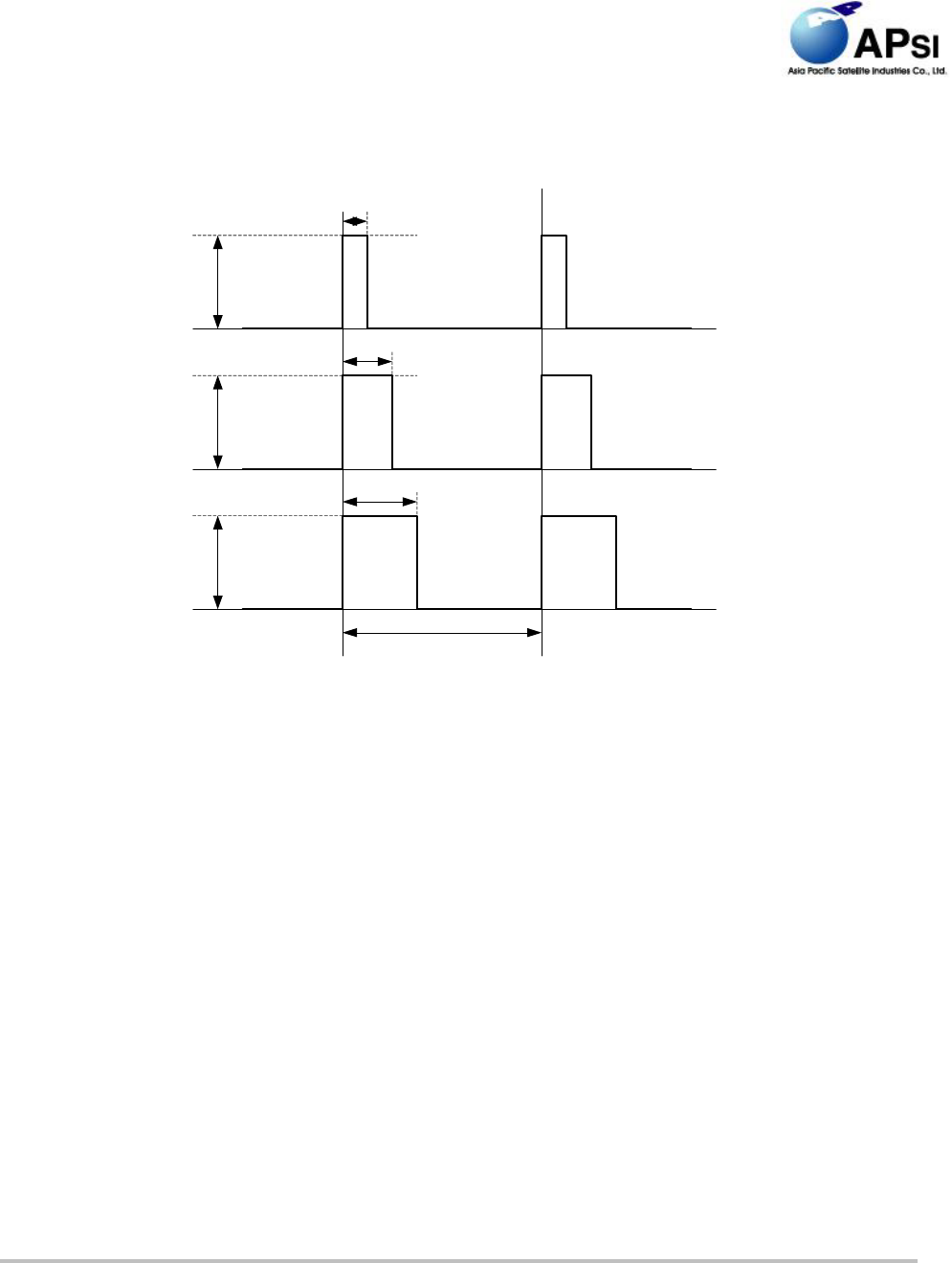
Power consumption timing diagrams is in figure 3 at talk time.
5 ms
10 ms
15 ms
40 ms
MAX 1.5A (5V)
MAX 1.5A (5V)
MAX 1.5A (5V)
Voice Call(TCH3)
Data/FAX(TCH6)
Data/FAX(TCH9)
Figure 3 5V_TX timing diagrams on each talk mode
3.3 Power supply solutions of various application
User should select power device by regarding the following items as suitting to the character of each
power when designs power supply.
1. Ripple noise should be ignorable
2. Transient response should be good quality
3. Whether output current enable to support enough current to each PIN
4. Whether accuracy is guaranteed
5. Whether PCB space suit to the condition required
6. Whether proper cost is required
There are some alternative devices for SAT module power supply solutions. The most common are
described in below.
1. Linear voltage regulators (Section 5.3.1)
2. Switched DC/DC converter (Section 5.3.2)
3. 1-cell Li-Ion battery (Section 5.3.3)
3.3.1 Linear voltage regulators
Linear regulators has good quality of ripple noise and output accuracy, so power supply with linear
regulators is easy to design, and the total cost for the components can be low, but efficiency is so bad
THURAYA Second-Generation User Terminal
SM-2500 Technical Information Manual
Document No.: AP01-601-08
+Update: 02/11/06 Ver: 0.8 Page 11 of 21
This page contains confidential information, which is protected by copyright and is proprietary to APSI.
No part of this document may be used, copied, disclosed or conveyed to another party without prior written consent of APSI
when the difference input voltage and output voltage is big.
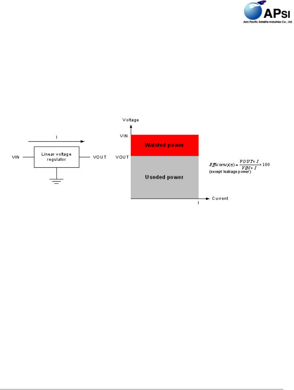
Ideally if the desired output voltage is 5V and the input voltage is 15V, ideal 10V goes away as heat, so
efficiency is only 30%. Therefore linear voltage regulator is necessary to effective cooling element in case
of big power dissipations.
We recomed linear voltage regulators only use when the difference input voltage and output
voltage is below 1V
Figure 4 Ideally efficiency of linear voltage regurator
3.3.2 Switched DC/DC converter
A switched DC/DC converter is very often used when there are requirements for high efficiency.
If you design the power supply what input voltage is above 15V and output voltage only is 5V, you need
to the many cooling equipments because of a lot of heat. This problem can be resolved by using a
switched DC/DC converter of high effiency.
There are instead a lot of other things to consider when design with switched DC/DC converter.
1. Need to many parts of inductor, diode, big size capacitor etcs.
2. PCB artwork must be very well because around a switched DC/DC converter there are magnetic fields,
which can create disturbances to other electronic circuits.
3. Circuit is designed that it is suppressed the ripple noise created by switching of MOSFET.
3.3.3 Battery
1-cell Li-Ion battery is general power equipment which is mostly used at the handheld goods.
THURAYA Second-Generation User Terminal
SM-2500 Technical Information Manual
Document No.: AP01-601-08
+Update: 02/11/06 Ver: 0.8 Page 12 of 21
This page contains confidential information, which is protected by copyright and is proprietary to APSI.
No part of this document may be used, copied, disclosed or conveyed to another party without prior written consent of APSI
When using a Li-Ion battery the battery must be able to deliver all necessary power peaks to the SAT
module.
The pack incorporates a protection circuit capable of detecting overvoltage (protection against
overcharging), undervoltage (protection against deep discharging) and overcurrent. Overcurrent detecting
range should be setted as supply sufficient current
The internal resistance of the battery and the protection circuits should be as low as possible because
internal resistance is very proportioned the voltage drop. It is recommended not to exceed 100mΩ, even
under extreme conditions at low temperature.
The battery pack must be approved to satisfy the requirements of CE.
4 Control signals
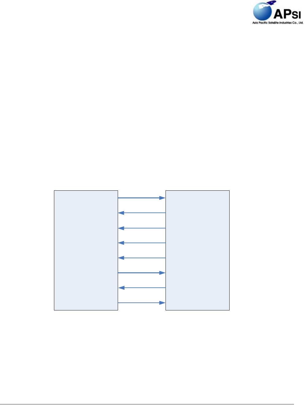
There are 6-pins for control SAT module. It is pins for GM_ON, GM_OFF, /GM_RESET,
GM_WAKEUP, HOST_WAKEUP, GM_STATUS, and HOST_STATUS.
The status of SAT mudule and HOST is shown in Figure 7 according to each of the control signals timing.
SAT
module HOST
UART_TXD
GM_ON
UART_RXD
GM_OFF
/GM_RESET
GM_STATUS
GM_WAKEUP
HOST_WAKEUP
Figure .Connection diagram of control signals
THURAYA Second-Generation User Terminal
SM-2500 Technical Information Manual
Document No.: AP01-601-08
+Update: 02/11/06 Ver: 0.8 Page 13 of 21
This page contains confidential information, which is protected by copyright and is proprietary to APSI.
No part of this document may be used, copied, disclosed or conveyed to another party without prior written consent of APSI
5 RTC backup battery interface
RTC (Real Time Clock) power of SAT module is supplied by VRTC pin of board-to-board connector.
VRTC is used power souce of internal RTC block and GPS chipset.
External backup battery should be connected at VRTC pin because there’s no supply of internal power in
VRTC pin. When RTC backup battery is not used, it should be connected with VPWR or VEXT. Because,
if this pin isn’t connected with any power source, SAT module doesn’t operate.
Electrical character of VRTC pin is as below.
Vmax = +5.5V
Vmin = +2.0V
Vnorm = +3V
Idd = 15 ㎂ (max)
6 UART interface
SAT module offers two UART ports. One provides 8-full-pins communications and the other one
provides only 4 pins.
Driving current of each pin and voltage level of UART port are as follows.
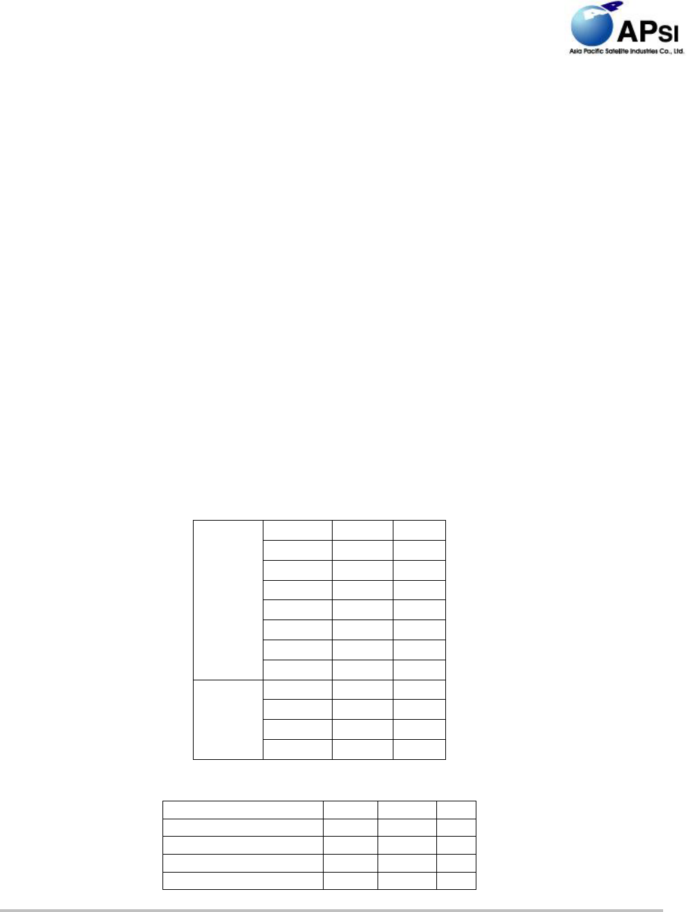
Table 4 Max driving current of each UART pins
TXD 2 ㎃
RXD 20 ㎂
CTS 20 ㎂
RTS 2 ㎃
DSR 20 ㎂
DTR 4 ㎃
DCD 8 ㎃
UART1
RI 8 ㎃
TXD 8 ㎃
RXD 20 ㎂
CTS 20 ㎂
UART2
RTS 8 ㎃
Table 5 Logic level of UART port
min max
Logic high input 2.1 3.3 V
Logic low input 0 0.9 V
Logic high output 2.4 3 V
Logic low output 0 0.6 V

THURAYA Second-Generation User Terminal
SM-2500 Technical Information Manual
Document No.: AP01-601-08
+Update: 02/11/06 Ver: 0.8 Page 14 of 21
This page contains confidential information, which is protected by copyright and is proprietary to APSI.
No part of this document may be used, copied, disclosed or conveyed to another party without prior written consent of APSI
7 USB interface
SAT module supports Revision 1.1 of Universal Serial Bus Specification.
8 AUDIO interface
8.1 CODEC selection
SAT module offers analog audio interface and digital audio interface.
Using or not of digital audio interface is decided by voltage level of CODEC_SEL pin.
If CODEC_SEL pin is ‘high’ level, then internal PCM CODEC is disabled and you can use external
PCM CODEC. If CODEC_SEL pin is ‘low’ level, then internal PCM CODEC is used. If you make
float CODEC_SEL pin, GEM module is using internal PCM CODEC.
When SAT module use internal PCM CODEC, you must make float DAI_DIN, DAI_DOUT, DAI_CLK,
and DAI_SYNC pins.
The spec for a pin being ‘High’ must be stated – the voltage rise time etc.
8.2 Digital Audio Interface
SAT module supply DAI for various audio applications.
The digital audio interface consist of data input (DAI_DIN), data output (DAI_DOUT), clock output
(DAI_CLK), and frame sync. (DAI_SYNC).
DAI_CLK : generated as 2.048MHz clock from SAT module.
DAI_SYNC : generated as 8kHz clock from SAT module.
DAI_DIN : received to 16-bits data from MSB bit to LSB bit at rising edge of clock.
DAI_DOUT: transmitted 16-bits data from MSB bit to LSB bit at rising edge of clock.
9 SIM card interface
SAT module requires a SIM card to operate in SAT mode (except for emergency call).
Support to the standard plug-in SIM card as defined in ETSI standard GSM 11.11, as modified by GSM 11.12.
Both 1.8V/3.0V and 3.0V only SIM cards are supported.
Table .SIM card interface pins function description

THURAYA Second-Generation User Terminal
SM-2500 Technical Information Manual
Document No.: AP01-601-08
+Update: 02/11/06 Ver: 0.8 Page 15 of 21
This page contains confidential information, which is protected by copyright and is proprietary to APSI.
No part of this document may be used, copied, disclosed or conveyed to another party without prior written consent of APSI
10 LCD interface
SAT module provides 14-pins interface with a LCD.
Specific characteristics are as below.
1. Supports 128*128 dot, 65k color LCD.
2. Using 8080-series 8bits parallel bus interface.
2. Supply LCD_ EN for control main power of LCD.
4. Support LCD driver IC: S6B33B6
11 Backlight interface
3-pins are used to control backlight of keypad and LCD in SAT module.
Table .Backlight interface pins function description
12 Keypad interface
SAT module provides keypad interface of 5*5 matrix scan method.
All of functions of module can be controlled by keypad.
SIM_VDD SIM card power supply.
1.8V(MAX:±10%)/3V(MAX:±10%) SIM card auto detect, provided by SAT module.
SIM_CLK SIM card clock, provided by SAT module.
SIM_RST SIM card reset, provided by SAT module.
SIM_DATA SIM card data line, input and output.
LCD_BL_EN LCD backlight enable (Active HIGH)
LCD_BL_DIM LCD backlight dimming control (PWL signal output)
KEYPAD_BL_EN KEYPAD backlight enable (Active HIGH)
THURAYA Second-Generation User Terminal
SM-2500 Technical Information Manual
Document No.: AP01-601-08
+Update: 02/11/06 Ver: 0.8 Page 16 of 21
This page contains confidential information, which is protected by copyright and is proprietary to APSI.
No part of this document may be used, copied, disclosed or conveyed to another party without prior written consent of APSI
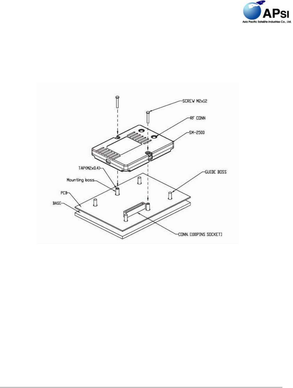
13Mechanical interface
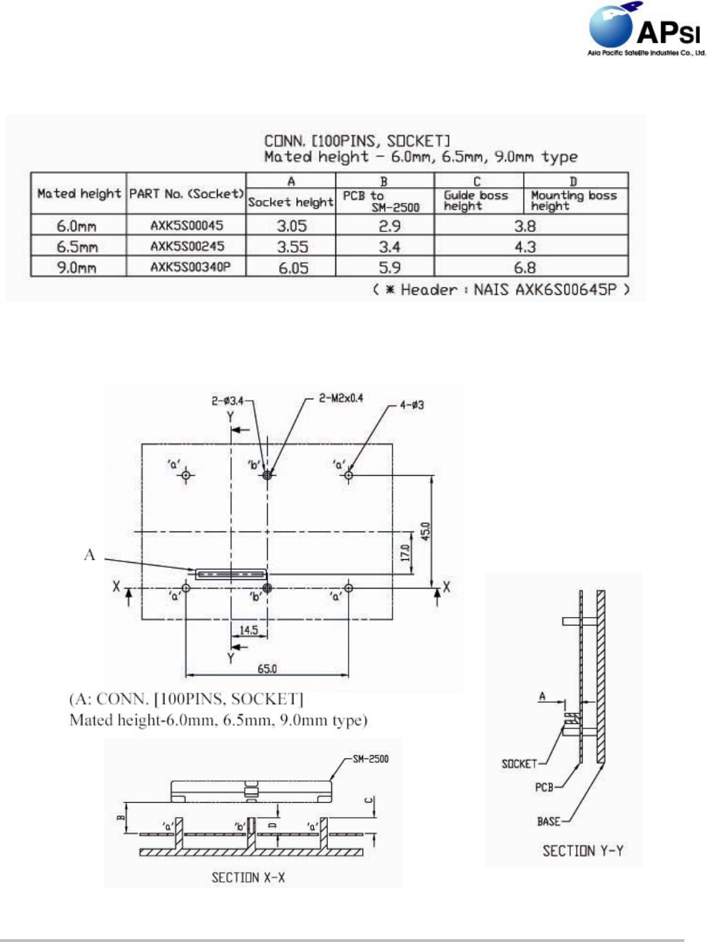
The Figure 37 shows the mechanical interfaces of SM-2500 Recommended board to board
female connector are also shown in Table 15. It’s the recommended base in Figure 38.
Mechanical interface
THURAYA Second-Generation User Terminal
SM-2500 Technical Information Manual
Document No.: AP01-601-08
+Update: 02/11/06 Ver: 0.8 Page 17 of 21
This page contains confidential information, which is protected by copyright and is proprietary to APSI.
No part of this document may be used, copied, disclosed or conveyed to another party without prior written consent of APSI
Recommended Board to Board Female connector
Figure .Recommended Base
THURAYA Second-Generation User Terminal
SM-2500 Technical Information Manual
Document No.: AP01-601-08
+Update: 02/11/06 Ver: 0.8 Page 18 of 21
This page contains confidential information, which is protected by copyright and is proprietary to APSI.
No part of this document may be used, copied, disclosed or conveyed to another party without prior written consent of APSI
14HEAT DISSIPATION
14.1 Installation method of Heat Sink
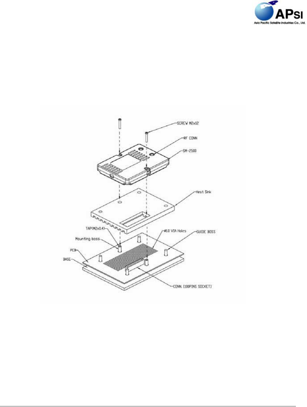
The proper method of heat dissipation to avoid overheating is necessary when SM-2500 is used
in the closed space. Installation of HEAT SINK is recommended between PCB and SM-2500 as
shown in the following figure.
Figure 5 Installation method of Heat Sink
14.2 Guide of HEAT SINK and PCB design
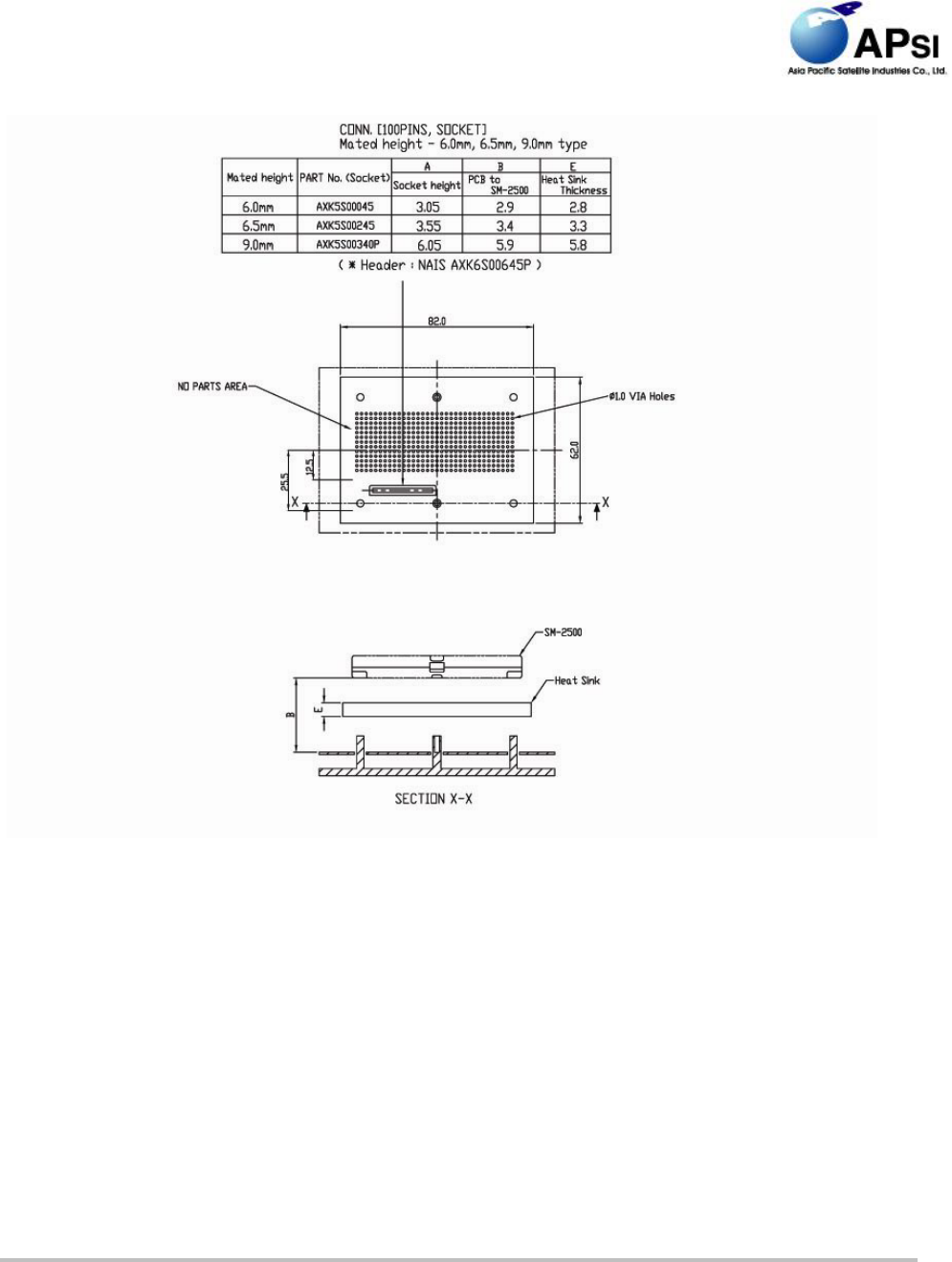
The thickness of HEAT SINK should be changed depending on MATED HEIGHT as shown in
the following figure.
The parts should not be located on the PCB surface including B2B connector contacting with
Heat sink for SM-2500 and VIA hole during PCB design should be created on PCB as many as
possible for good heat dissipation regarding the PCB area shown in the following figure.
THURAYA Second-Generation User Terminal
SM-2500 Technical Information Manual
Document No.: AP01-601-08
+Update: 02/11/06 Ver: 0.8 Page 19 of 21
This page contains confidential information, which is protected by copyright and is proprietary to APSI.
No part of this document may be used, copied, disclosed or conveyed to another party without prior written consent of APSI
Figure .Guide of HEAT SINK and PCB design
The housing or case including SM-2500 and Heat Sink should be the material having good
thermal conductivity such as Aluminum and keep a good thermal contact between SM-2500 and
Heat Sink, and between the Heat Sink and outside housing.
14.3
THURAYA Second-Generation User Terminal
SM-2500 Technical Information Manual
Document No.: AP01-601-08
+Update: 02/11/06 Ver: 0.8 Page 20 of 21
This page contains confidential information, which is protected by copyright and is proprietary to APSI.
No part of this document may be used, copied, disclosed or conveyed to another party without prior written consent of APSI
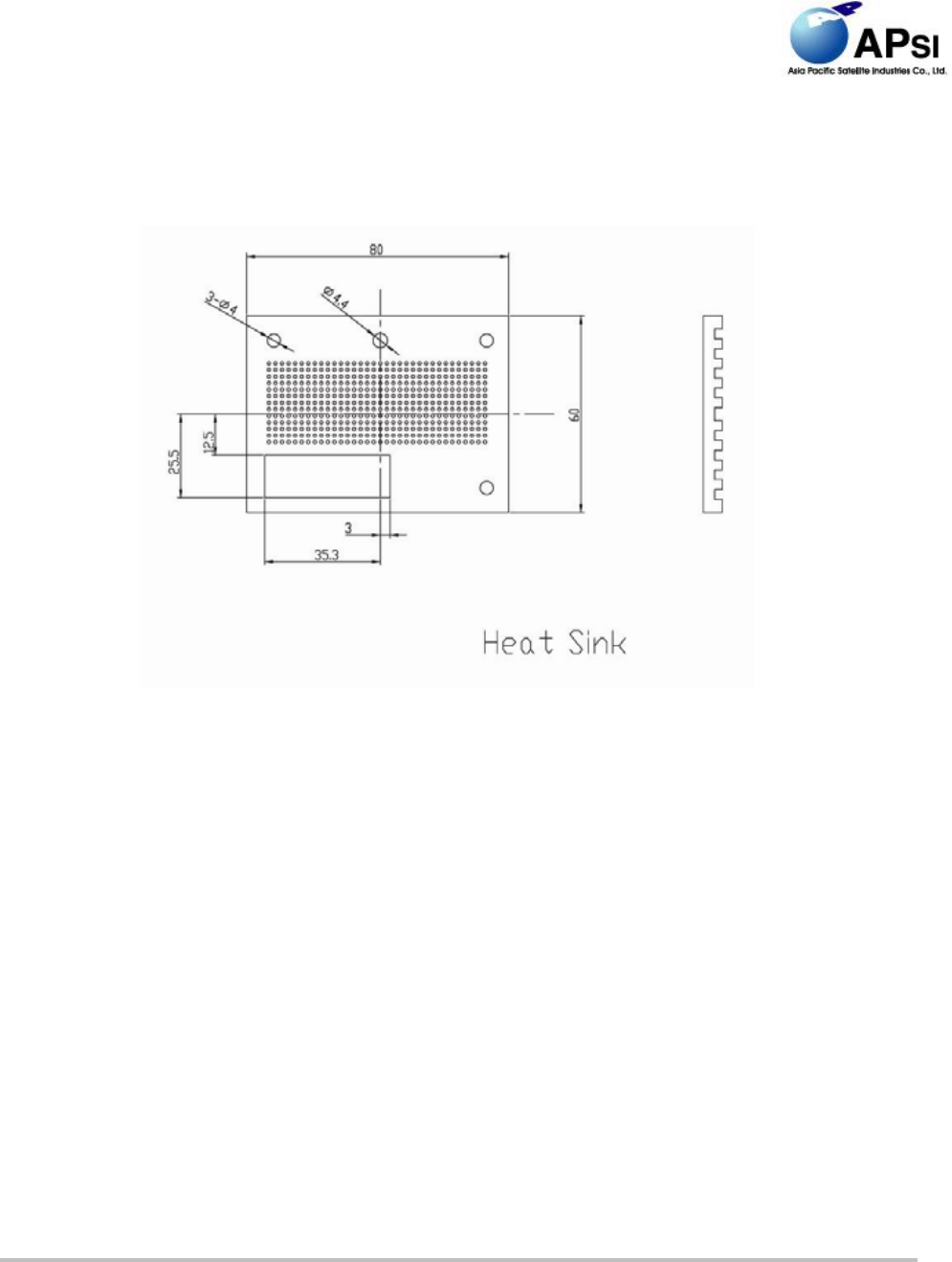
The material like Aluminum which has good thermal conductivity should be used. The following
figure is the example and size of heat sink for SM-2500.
Figure .Example of HEAT SINK Design

THURAYA Second-Generation User Terminal
SM-2500 Technical Information Manual
Document No.: AP01-601-08
+Update: 02/11/06 Ver: 0.8 Page 21 of 21
This page contains confidential information, which is protected by copyright and is proprietary to APSI.
No part of this document may be used, copied, disclosed or conveyed to another party without prior written consent of APSI
15Regulatory Information
15.1 NOTICES TO USER
This device complies with Part 15 of the FCC Rules. Operation is subject to the following two
conditions:
(1) this device may not cause harmful interference, and (2) this device must accept any
interference received, including interference that may cause undesired operation.
15.2 FCC WARNING
This equipment generates or uses radio frequency energy. Changes or modifications to this
equipment may cause harmful interference unless the modifications are expressly approved by
Asia Pacific Satellite Industries Co., Ltd. The user could lose the authority to operate this
equipment if an unauthorized change or modification is made.
15.3 INFORMATION TO THE USER
This equipment has been tested and found to comply with the limits for a Class B digital device,
pursuant to Part 15 of the FCC Rules.
These limits are designed to provide reasonable protection against harmful interference in a
residential installation.
This equipment generates, uses and can generate radio frequency energy and, if not installed
and
used in accordance with the instructions, may cause harmful interference to radio
communications. However, there is no guarantee that the interference will not occur in a
particular
installation. If this equipment does cause harmful interference to radio or television reception,
which can be determined by turning the equipment off and on, the user is encouraged to try to
correct the interference by one or more of the following measures:
· Reorient or relocate the receiving antenna.
· Increase the separation between the equipment and receiver.
· Connect the equipment to an outlet on a circuit different from that to which the receiver is
connected.
· Consult the dealer for technical assistance.
IMPORTANT NOTE:
FCC Radiation Exposure Statement:
This equipment complies with FCC radiation exposure limits set forth for an uncontrolled
environment. This equipment should be installed and operated with minimum distance of 20cm
between the radiator and your body.
This transmitter must not be co-located or operating in conjunction with any other antenna or
transmitter.