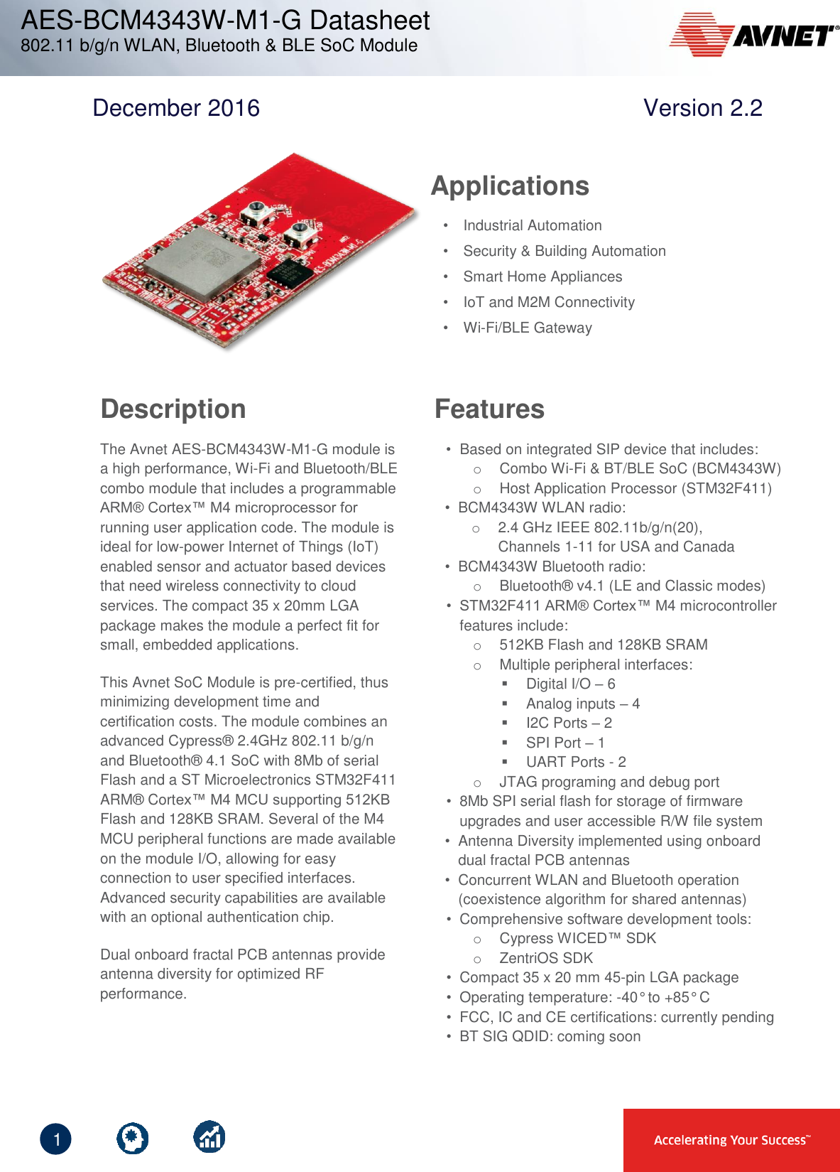
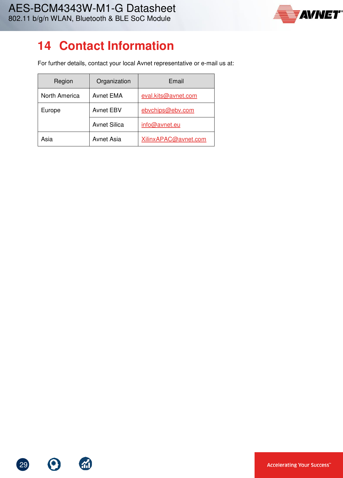
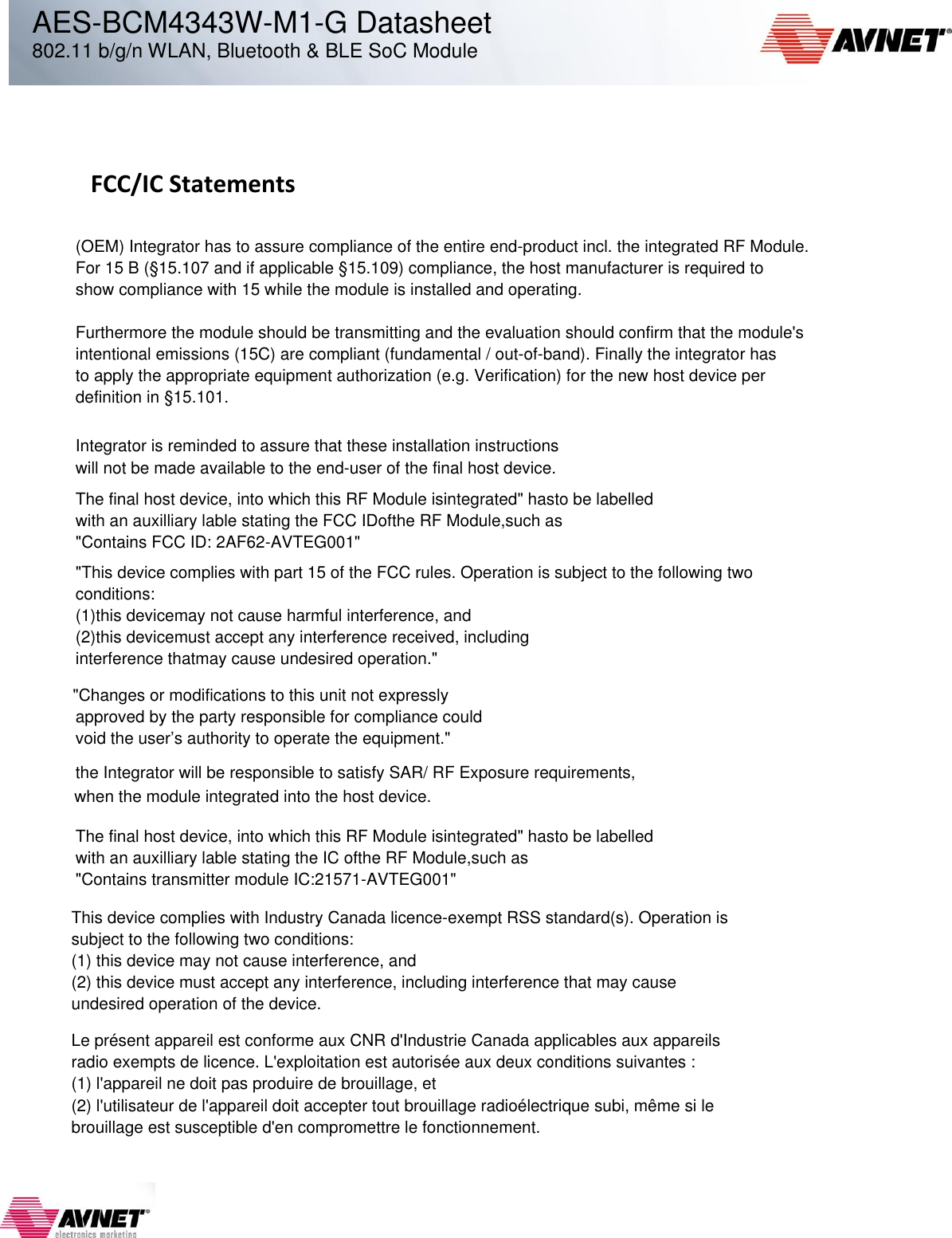
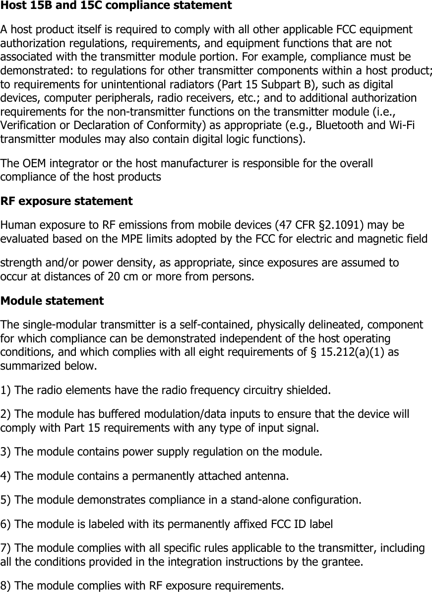
Avnet AVTEG001 WLAN and BT LE Module User Manual Data sheet

Avnet Inc WLAN and BT LE Module Data sheet

Data sheet

   1    1 AES-BCM4343W-M1-G Datasheet 802.11 b/g/n WLAN, Bluetooth & BLE SoC Module December 2016                         Version 2.2  Description  Features The Avnet AES-BCM4343W-M1-G module is a high performance, Wi-Fi and Bluetooth/BLE combo module that includes a programmable ARM® Cortex™ M4 microprocessor for running user application code. The module is ideal for low-power Internet of Things (IoT) enabled sensor and actuator based devices that need wireless connectivity to cloud services. The compact 35 x 20mm LGA package makes the module a perfect fit for small, embedded applications.  This Avnet SoC Module is pre-certified, thus minimizing development time and certification costs. The module combines an advanced Cypress® 2.4GHz 802.11 b/g/n and Bluetooth® 4.1 SoC with 8Mb of serial Flash and a ST Microelectronics STM32F411 ARM® Cortex™ M4 MCU supporting 512KB Flash and 128KB SRAM. Several of the M4 MCU peripheral functions are made available on the module I/O, allowing for easy connection to user specified interfaces. Advanced security capabilities are available with an optional authentication chip.  Dual onboard fractal PCB antennas provide antenna diversity for optimized RF performance.   •  Based on integrated SIP device that includes: o  Combo Wi-Fi & BT/BLE SoC (BCM4343W) o  Host Application Processor (STM32F411) •  BCM4343W WLAN radio: o 2.4 GHz IEEE 802.11b/g/n(20),  Channels 1-11 for USA and Canada •  BCM4343W Bluetooth radio: o  Bluetooth® v4.1 (LE and Classic modes) • STM32F411 ARM® Cortex™ M4 microcontroller features include: o  512KB Flash and 128KB SRAM  o  Multiple peripheral interfaces:    Digital I/O – 6    Analog inputs – 4    I2C Ports – 2    SPI Port – 1    UART Ports - 2  o  JTAG programing and debug port  •  8Mb SPI serial flash for storage of firmware upgrades and user accessible R/W file system  •  Antenna Diversity implemented using onboard dual fractal PCB antennas •  Concurrent WLAN and Bluetooth operation (coexistence algorithm for shared antennas) •  Comprehensive software development tools:  o  Cypress WICED™ SDK  o  ZentriOS SDK •  Compact 35 x 20 mm 45-pin LGA package •  Operating temperature: -40° to +85° C •  FCC, IC and CE certifications: currently pending •  BT SIG QDID: coming soon    Applications •  Industrial Automation  •  Security & Building Automation  •  Smart Home Appliances  •  IoT and M2M Connectivity • Wi-Fi/BLE Gateway
   2    2 AES-BCM4343W-M1-G Datasheet 802.11 b/g/n WLAN, Bluetooth & BLE SoC Module Document Control  Document Version: Version 2.2 Document Date: 23 December 2016 Document Author(s): JB, PF Document Classification: Released Document Distribution: Public Prior Version History: Version: Date: Comment: 0.1 5/2/16 Initial release 0.2 5/2/16 Updated Module Features 0.3 5/2/16 Added SPI flash and Antenna details 1.0 6/27/16 Tape & Reel Packaging and Antenna Options sections updated 2.0 11/16/16 Specs for low-power modes added References to Broadcom removed Reference to BT/BLE 4.2 removed Option of using external antennas removed  2.1 12/19/16 Miscellaneous updates. Wi-Fi and BT versions and channel detail noted  2.2 12/23/16 256-QAM (TurboQAM) mode removed Data rate max reduced to 65 Mbps  Regional contact info updated Comments:
   3    3 AES-BCM4343W-M1-G Datasheet 802.11 b/g/n WLAN, Bluetooth & BLE SoC Module 1  Table of Contents 2 Table of Figures .................................................................................................... 5 3 Functional Overview.............................................................................................. 6 3.1 Microcontroller .......................................................................................................... 6 3.2 SPI Flash Memory .................................................................................................... 6 3.3 WLAN ...................................................................................................................... 7 3.4 Bluetooth .................................................................................................................. 7 3.5 Antennas .................................................................................................................. 7 4 Block Diagram ....................................................................................................... 8 5 Module Pin Descriptions ....................................................................................... 9 5.1 Pin Descriptions ....................................................................................................... 9 5.2 Pin Definitions ........................................................................................................ 10 6 Electrical Specifications ...................................................................................... 11 6.1 Absolute Maximum Ratings .................................................................................... 11 6.2 Recommended Operating Conditions ..................................................................... 11 6.3 Power Supply Requirements .................................................................................. 11 6.4 WLAN Power Consumption .................................................................................... 12 6.5 Bluetooth Power Consumption ............................................................................... 12 6.6 Bluetooth Low Energy Power Consumption ........................................................... 12 6.7 Low Power Modes Power Consumption ................................................................. 12 7 RF Specifications ................................................................................................ 13 7.1 WLAN RF Characteristics....................................................................................... 13 7.1.1 Transmitter Specification ....................................................................................................14 7.1.2 Receiver Specification ........................................................................................................15 7.2 Bluetooth RF Characteristics .................................................................................. 17 7.2.1 Transmitter Specification ....................................................................................................17 7.2.2 Receiver Specification ........................................................................................................17 7.3 BLE RF Characteristics .......................................................................................... 18 8 Mechanical Specifications ................................................................................... 19 8.1 Mechanical Size ..................................................................................................... 19 8.2 Module PCB Footprint ............................................................................................ 20 8.3 Module Pad Size .................................................................................................... 20 8.4 Recommended Solder Paste Mask ........................................................................ 21 8.5 Recommended Solder Mask .................................................................................. 21 8.6 Tape and Reel Packaging ...................................................................................... 22 9 Soldering and Cleaning Recommendations ........................................................ 23 9.1 Optimum Soldering Reflow Profile .......................................................................... 23
   4    4 AES-BCM4343W-M1-G Datasheet 802.11 b/g/n WLAN, Bluetooth & BLE SoC Module 9.2 Cleaning ................................................................................................................. 23 10 Antennas ............................................................................................................. 24 11 Certifications ....................................................................................................... 25 11.1 RoHS ..................................................................................................................... 25 11.2 Regulatory Compliance .......................................................................................... 25 11.3 Bluetooth Interoperability Compliance .................................................................... 25 11.4 Regulatory Agency Statements .............................................................................. 25 11.5 OEM Instructions .................................................................................................... 26 11.6 OEM Labeling Requirements ................................................................................. 26 11.7 Limitations .............................................................................................................. 26 12 Shipping, Handling and Storage ......................................................................... 27 12.1 Shipping ................................................................................................................. 27 12.2 Handling ................................................................................................................. 27 12.3 Moisture Sensitivity (MSL) ...................................................................................... 27 12.4 Storage .................................................................................................................. 27 13 Ordering Information ........................................................................................... 28 13.1 Module Accessories ............................................................................................... 28 14 Contact Information ............................................................................................. 29
   5    5 AES-BCM4343W-M1-G Datasheet 802.11 b/g/n WLAN, Bluetooth & BLE SoC Module 2  Table of Figures Figure 1 – AES-BCM4343W-M1-G Module Block Diagram .................................................................... 8 Figure 2 – AES-BCM4343W-M1-G Module Top View .......................................................................... 19 Figure 3 – AES-BCM4343W-M1-G Module Side View ......................................................................... 19 Figure 4 – AES-BCM4343W-M1-G Module PCB Footprint ................................................................... 20 Figure 5 – AES-BCM4343W-M1-G Module Pad Size ........................................................................... 20 Figure 6 – Recommended Solder Paste Mask Size ............................................................................. 21 Figure 7 – Recommended Solder Mask Size ........................................................................................ 21 Figure 8 – Tape Dimensions ................................................................................................................. 22 Figure 9 – Recommended Soldering Profile for Lead-Free Solder ....................................................... 23 Figure 10 – Dual Fractal PCB Antennas ............................................................................................... 24 Figure 11 – Test Probe Connectors (Murata SWD series) ................................................................... 24
   6    6 AES-BCM4343W-M1-G Datasheet 802.11 b/g/n WLAN, Bluetooth & BLE SoC Module 3  Functional Overview This 2.4GHz wireless module provides a complete combo Wi-Fi/BT/BLE and MCU solution for cost-effective embedded-wireless IoT applications. Based on latest-generation Cypress BCM4343W Wireless SoC silicon, this high performance combo module provides a unique solution with Wi-Fi and Bluetooth radios, ARM Cortex-M4 host processor and expansion SPI Flash memory, plus versatile dual onboard and dual external antenna capabilities, all in a compact 35 mm x 20 mm, easy to mount (0.1” pitch LGA) form-factor module, qualified for operation across the full industrial temperature range      3.1  Microcontroller The AES-BCM4343W-M1-G module includes an on-board microcontroller (MCU) that interfaces with the Cypress BCM4343W radio for communication and acts as the system controller for user applications. Based on the ST Microelectronics STM32F411, the MCU supports the following features:   STM32F411 ARM 32-bit Cortex™-M4 (with FPU), @ 100 MHz  On-chip memory: 512 kbytes Flash, 128 Kbytes SRAM   Multiple serial communication interfaces: SPI, USART, PCM   Sensor applications support: ADC, I2C, I2S, GPIO, Timers   Cypress WICED SDK and ZentriOS SDK based cloud connected application examples are provided (AWS IoT, IBM Bluemix, ThingSpeak and others…)   Debug support: JTAG interface Application code for the module can be developed using Cypress’s WICED Software Development Kit (SDK) or Zentri’s ZentriOS SDK.  Additional details on the STM32F411 MCU features, specifications, and programming modes can be obtained from the STM32F411 datasheet.  3.2  SPI Flash Memory An 8 Mbit SPI Flash memory (Macronix MX25L800EZUI12G) is included on the module for the storage of BCM4343W firmware, static webpages, built-in documentation, images, etc. The STM32F411 MCU’s SPI1 peripheral interface, clocked at 50MHz, is used to communicate with this memory.   The SPI1 interface parameters are defined in the BCM94343W_AVN platform files of the Cypress WICED SDK development environment. When building an application in WICED SDK, adding the download_apps parameter to the make target command string, ensures that the BCM4343W firmware is written to- and loaded from this SPI flash     MCU WICED SDK SPI1 Signal Name Pin Name Pin Name SPI_FLASH_CS PA4 WICED_GPIO_5 SPI_FLASH_CLK PA5 WICED_GPIO_6 SPI_FLASH_MISO PA6 WICED_GPIO_7 SPI_FLASH_MOSI PA7 WICED_GPIO_8
   7    7 AES-BCM4343W-M1-G Datasheet 802.11 b/g/n WLAN, Bluetooth & BLE SoC Module 3.3  WLAN   Cypress BCM4343W combo single-chip MAC, Baseband and RF device  (includes ARM Cortex-M3 processor)    Frequency Band: Single-band, 2.4 GHz only    WLAN Network Standards supported: 802.11b, 802.11g, 802.11n (single stream)    Modulation Modes: CCK and OFDM with BPSK, QPSK, 16QAM, 64QAM    Supported Data Rates:  - IEEE 802.11b  1 – 11 Mbps - IEEE 802.11g  6 – 54 Mbps - IEEE 802.11n  7.2 – 65 Mbps (2.4 GHz only)    Hardware Encryption  - WEP, WPA / WPA2 Personal    Advanced 1x1 802.11n Features:  - Full/Half Guard Interval - Frame Aggregation - Space Time Block Coding (STBC) - Low Density Parity Check (LDPC) Encoding    SDIO host interface for WLAN subsystem (between BCM4343W and STM32F411 MCU)    Optional WLAN Debug Interfaces:  - WLAN JTAG and WLAN Debug UART interfaces are pinned-out to support special cases   (most application development will not require this)  3.4 Bluetooth   Bluetooth 4.1 (supporting Bluetooth Low Energy) with backward compatibility   Bluetooth Smart Ready (support for Dual-mode Bluetooth Classic and BLE operation)   Advanced Algorithm for support of Bluetooth/BLE and Wi-Fi coexistence  (for concurrent WLAN and Bluetooth operation)   Dedicated high-speed UART for Bluetooth host interface  3.5  Antennas   Onboard dual fractal PCB antennas (Cypress patented PCB trace antennas)   Miniature switched RF connectors. These are for test purposes only!     Transmit and Receive antenna diversity
   8    8 AES-BCM4343W-M1-G Datasheet 802.11 b/g/n WLAN, Bluetooth & BLE SoC Module 4  Block Diagram Figure 1 shows a functional block diagram of the AES-BCM4343W-M1-G module.   Figure 1 – AES-BCM4343W-M1-G Module Block Diagram
   9    9 AES-BCM4343W-M1-G Datasheet 802.11 b/g/n WLAN, Bluetooth & BLE SoC Module 5  Module Pin Descriptions 5.1  Pin Descriptions  MCU WICED SDKPinNo.Signal Name TypePinNamePinName Description*1 GND SIG - - Ground2 MICRO_I2C2_SCL I/O PB10 WICED_GPIO_20 I2C #2 SCL3 MICRO_I2C2_SDA I/O PB11 WICED_GPIO_21 I2C #2 SDA4 MICRO_SPI2_SCK I/O PB13 WICED_GPIO_23 SPI #2 SCK5 MICRO_SPI2_SSN I/O PB12 WICED_GPIO_22 SPI #2 SSN6 MICRO_SPI2_MISO I/O PB14 WICED_GPIO_24 SPI #2 MISO7 MICRO_SPI2_MOSI I/O PB15 WICED_GPIO_25 SPI #2 MOSI8 USART6_TX_I2S2_MCK I/O PC6 WICED_GPIO_13 USART #6 TX9 USART6_RX_I2S2_CK I/O PC7 WICED_GPIO_14 USART #6 RX10 MICRO_UART_TX I/O PA9 WICED_GPIO_9 USART #1 TX11 MICRO_UART_RX I/O PA10 WICED_GPIO_10 USART #1 RX12 MICRO_UART_CTS I/O PA11 WICED_GPIO_15 USART #1 CTS13 MICRO_UART_RTS I/O PA12 WICED_GPIO_16 USART #1 RTS14 WIFI_GPIO_1 I/O PD13 -WLAN Tx/Rx Activty (Driven by GPIO_1 of BCM4343W device)15 GND SIG - - Ground16 VDD_3V3_SIP SIG - - 3.3V17 GND SIG - - Ground18 WL_JTAG_TDI N/C - - No Connect (requires hardware modification for connection)19 WL_JTAG_TDO N/C - - No Connect (requires hardware modification for connection)20 MICRO_JTAG_TMS I/O PA13 - JTAG TMS21 MICRO_JTAG_TCK I/O PA14 - JTAG TCK22 MICRO_JTAG_TDI I/O PA15 - JTAG TDI23 MICRO_JTAG_TDO I/O PB3 - JTAG TDO24 MICRO_JTAG_TRSTN I/O PB4 - JTAG RESETN25 GND SIG - - Ground26 VBAT_SIP SIG - - Power supply for backup when VDD_3V3_SIP is not present27 GND SIG - - Ground28 MICRO_I2C1_SCL I/O PB6 WICED_GPIO_11 I2C #1 SCL29 MICRO_I2C1_SDA I/O PB7 WICED_GPIO_12 I2C #1 SDA30 MICRO_GPIO_3 I/O PC1 WICED_GPIO_27 GPIO 331 MICRO_GPIO_2 I/O PC0 WICED_GPIO_26 GPIO 232 MICRO_GPIO_4 I/O PC2 WICED_GPIO_28 GPIO 433 MICRO_GPIO_5 I/O PC3 WICED_GPIO_17 GPIO 534 MICRO_GPIO_6 I/O PB9 WICED_GPIO_19 GPIO 635 MICRO_GPIO_1 I/O PB8 WICED_GPIO_18 GPIO 136 MICRO_RST_N I/O NRST RESET_N37 MICRO_ADC_IN1 I/O PA1 WICED_GPIO_2 ADC INPUT #138 MICRO_WKUP I/O PA0 WICED_GPIO_1 MCU WAKEUP39 GND SIG - - Ground40 MICRO_ADC_IN2 I/O PA2 WICED_GPIO_3 ADC INPUT #241 MICRO_ADC_IN3 I/O PA3 WICED_GPIO_4 ADC INPUT #342 MICRO_GPIO_0 I/O PB0 WICED_GPIO_29 GPIO 043 MICRO_ADC_IN15 I/O PC5 WICED_GPIO_30 ADC INPUT #1544 GND SIG - - Ground45 GND SIG - - GroundModule - Denotes 5V tolerant I/O - Standard 3.3V I/O - Bidirection reset pin with embedded weak pullup* Note the pin descriptions shown are arbitrary for most MCU connected signals
   10    10 AES-BCM4343W-M1-G Datasheet 802.11 b/g/n WLAN, Bluetooth & BLE SoC Module 5.2 Pin Definitions Of the 44 pads located along 3 edges of the module, 8 connect to GND and 2 are power connections Most of the remaining module pads are internally connected to the STM32F411 MCU. For this reason, the signal definition of these pins is somewhat arbitrary given that the pin modes can be configured via software.   The signal names provided in the Pin Description table shown in section 4.1 align with the names provided in the Cypress WICED SDK platform.h file. Users have the ability to modify these configurations and definitions as explained in the STM32F411 datasheet.
   11    11 AES-BCM4343W-M1-G Datasheet 802.11 b/g/n WLAN, Bluetooth & BLE SoC Module 6  Electrical Specifications For electrical characteristics of the module digital I/O’s connected to the internal STM32F411 MCU, refer to the STM32F411 datasheet (Document ID 026289 Rev 4 or later). 6.1  Absolute Maximum Ratings  Parameter Min Max Unit VDD_3V3_SIP 0 4 Volts VBAT_SIP 0 4 Volts Voltage on Digital I/Os -0.3 4 Volts Voltage on Analog Inputs -0.3 4 Volts Supply Ripple -2 2 % Storage Temperature -40 +85 ºC Operating Temperature -40 +85 ºC  6.2  Recommended Operating Conditions  Parameter Min Typ Max Unit VDD_3V3_SIP 3.0 3.3 3.6 Volts VBAT_SIP 2.0 3.3 3.6 Volts Voltage on Digital I/Os 0 3.3 VDD_3V3_SIP Volts Voltage on Analog Inputs 0 3.3 VDD_3V3_SIP Volts Humidity Range* 0   95 % Operating Temperature -40 25 +85 ºC * Non-condensing, relative humidity  6.3  Power Supply Requirements  Parameter Min Typ Max Unit VDD_3V3_SIP 3.0 3.3 3.6 Volts VDD_3V3_SIP* - - - mA VBAT_SIP 2.0 3.3 3.6 Volts VBAT_SIP* - - - mA * See Power Consumption figures on next page
   12    12 AES-BCM4343W-M1-G Datasheet 802.11 b/g/n WLAN, Bluetooth & BLE SoC Module 6.4  WLAN Power Consumption Condition: 25deg.C, includes both Wi-Fi and Microcontroller Parameter Test Condition (+25 ºC, 3.3V) Min Typ Max Unit 11b Tx Mode 11 Mbps - 400  mA 11g Tx Mode 54 Mbps - 260  mA 11n Tx Mode MCS7 - 200  mA 11b Rx Mode 11 Mbps - 46  mA 11g Rx Mode 54 Mbps - 46  mA 11n Rx Mode MCS7 - 46  mA  6.5 Bluetooth Power Consumption Condition: 25deg.C, includes Both Wi-Fi/BT and Microcontroller Parameter Test Condition (+25 ºC, 3.3V) Min Typ Max Unit Tx Mode 3DH5 - 35  mA Rx Mode 3DH5 - 16  mA  6.6 Bluetooth Low Energy Power Consumption Condition: 25deg.C, includes Both Wi-Fi/BT and Microcontroller Parameter Test Condition (+25 ºC, 3.3V) Min Typ Max Unit Tx Mode Transmitter and baseband @ 100% - 35  mA Rx Mode Receiver and baseband @ 100% - 16  mA  6.7  Low Power Modes Power Consumption  Parameter  Device Test Condition  (+25 ºC, 3.3V) Min Typ Max Unit Sleep Mode STM32F411 BCM4343W - - -  122    1.48  uA mA  Power Down Mode STM32F411 BCM4343W - - - 6.6 6.0  mA uA  Idle, Unassociated STM32F411 BCM4343W - - - 8.6 366  mA uA
   13    13 AES-BCM4343W-M1-G Datasheet 802.11 b/g/n WLAN, Bluetooth & BLE SoC Module 7  RF Specifications 7.1  WLAN RF Characteristics  The AES-BCM4343W-M1-G module complies with the following WLAN features and standards. Features Description WLAN Standards IEEE 802 Part 11b/g/n (802.11b/g/n single stream n) Antenna Port Supports single antenna for Wi-Fi Frequency Band 2.400 - 2.484 GHz  The RF performance of the AES-BCM4343W-M1-G module is given as follows (@ 3.3V):  Features Description Frequency band 2.4000 - 2.497 GHz (2.4 GHz ISM Band) Number of selectable sub-channels 14 Channels Modulation OFDM, DSSS (Direct Sequence Spread Spectrum), DBPSK, DQPSK, CCK, 16QAM, 64QAM Supported rates 1, 2, 5.5, 11, 6, 9, 12, 24, 36, 48, 54 Mbps  & HT20 MCS 0~7 Maximum receive input level -10dBm (with PER < 8% @ 11 Mbps) -20dBm (with PER < 10% @ 54 Mbps) -20dBm (with PER < 10% @ MCS7) Output power 17dBm @ 802.11b 13dBM @ 802.11g 12dBM @ 802.11n Carrier frequency accuracy +/- 20 ppm (crystal: 26 MHz +/- 10 ppm @ 25 ºC)
   14    14 AES-BCM4343W-M1-G Datasheet 802.11 b/g/n WLAN, Bluetooth & BLE SoC Module 7.1.1  Transmitter Specification 7.1.1.1  802.11b Transmitter Specification Parameter Test Condition Min Typ Max Unit Transmit Output Power Level 1/2/5.5/11 Mbps - 17 - dBm Transmit Center Freq. Tolerance - -20 0 20 ppm Transmit Spectrum Mask Fc-22MHz<F<FC-11MHz & Fc+11MHz<F<Fc+22MHz (1/2/5.5/11 Mbps;  Channel 1~13) - - -30* dBr F<FC-22MHz & F>Fc+22MHz (1/2/5.5/11 Mbps;  Channel 1~13) - - -50* dBr Transmit Power-On 10% ~ 90% - 0.3 2* us Transmit Power-Down 90% ~ 10% - 1.5 2* us Transmit Modulation Accuracy 1/2/5.5/11 Mbps - -17 -10 dB             Note 1 - "*" Indicates IEEE802.11 specification          7.1.1.2  802.11g Transmitter Specification Parameter Test Condition Min Typ Max Unit Transmit Output Power Level 6/9/12/18/24/36/48/54 Mbps - 13 - dBm Transmit Center Freq. Tolerance - -20 0 20 ppm Transmit Modulation Accuracy 6 Mbps - - -5* dB 9 Mbps - - -8* dB 12 Mbps - - -10* dB 18 Mbps - - -13* dB 24 Mbps - - -16* dB 36 Mbps - - -19* dB 48 Mbps - - -22* dB 54 Mbps - - -25* dB Transmit Spectrum Mask @ 11 MHz - - -20* dBr @ 20 MHz - - -28* dBr @ 30 MHz - - -40* dBr             Note 1 - "*" Indicates IEEE802.11 specification
   15    15 AES-BCM4343W-M1-G Datasheet 802.11 b/g/n WLAN, Bluetooth & BLE SoC Module 7.1.1.3  802.11n Transmitter Specification Parameter Test Condition Min Typ Max Unit Transmit Output Power Level HT20 MCS 0~7 - 12 - dBm Transmit Center Freq. Tolerance - -20 0 20 ppm Transmit Modulation Accuracy HT20, MCS0~7 - - -27* dB Transmit Spectrum Mask @ 11 MHz - - -20* dBr @ 20 MHz - - -28* dBr @ 30 MHz - - -40* dBr             Note 1 - "*" Indicates IEEE802.11 specification          7.1.2  Receiver Specification 7.1.2.1  802.11b Receiver Specification Parameter Test Condition Min Typ Max Unit Receiver Minimum Input Level Sensitivity  (PER < 8%) 1 Mbps -80* -93 - dBm 2 Mbps -80* -91 - dBm 5.5 Mbps -76* -89 - dBm 11 Mbps -76* -86 - dBm Receiver Maximum Input Level Sensitivity  (PER < 8%) 1/2/5.5/11 Mbps -10* - - dBm             Note 1 - "*" Indicates IEEE802.11 specification
   16    16 AES-BCM4343W-M1-G Datasheet 802.11 b/g/n WLAN, Bluetooth & BLE SoC Module  7.1.2.2  802.11g Receiver Specification Parameter Test Condition Min Typ Max Unit Receiver Min. Input Level Sensitivity  (PER < 10%) 6 Mbps -82* -88 - dBm 9 Mbps -81* -87 - dBm 12 Mbps -79* -85 - dBm 18 Mbps -77* -83 - dBm 24 Mbps -74* -80.5 - dBm 36 Mbps -70* -78.5 - dBm 48 Mbps -66* -74 - dBm 54 Mbps -65* -72 - dBm Receiver Max. Input Level Sensitivity  (PER < 10%) 6/9/12/18/24/36/48/54 Mbps -20* - - dBm             Note 1 - "*" Indicates IEEE802.11 specification  7.1.2.3  802.11n Receiver Specification Parameter Test Condition Min Typ Max Unit Receiver Min. Input Level Sensitivity (PER < 10%) HT20, MSC0 -82* -87.5 - dBm HT20, MSC1 -79* -84 - dBm HT20, MSC2 -77* -82 - dBm HT20, MSC3 -74* -80.5 - dBm HT20, MSC4 -70* -77 - dBm HT20, MSC5 -66* -72 - dBm HT20, MSC6 -65* -71 - dBm HT20, MSC7 -64* -70 - dBm MSC0 ~ MSC7 -20* - - dBm Receiver Max. Input Level Sensitivity (PER < 10%) MSC0 ~ MSC7 -20* - - dBm
   17    17 AES-BCM4343W-M1-G Datasheet 802.11 b/g/n WLAN, Bluetooth & BLE SoC Module  7.2 Bluetooth RF Characteristics 7.2.1  Transmitter Specification Parameter Mode and Condition Min Typ Max Unit Transmitter Section Frequency Range - 2402.0 - 2480 MHz Output Power GFSK - 10 - dBm QPSK - 6 - dBm BPSK - 6 - dBm Power Control Step   2 4 8 dB Lo Performance Initial Carrier Freq. Tolerance - - +/-25 +/-75 KHz Lock Time - - 72 - uS Frequency Drift DH1 Packet - - +/-8 +/-25 KHz DH3 Packet - - +/-8 +/-40 KHz DH5 Packet - - +/-8 +/-40 KHz Drift Rate - - 5 20 KHz/50 us Frequency Deviation 00001111 Sequence in Payload (a) - 140 155 175 KHz 10101010 Sequence in Payload (b) - 115 140 - KHz Channel Spacing - - 1 - MHz             (a) This pattern represents an average deviation in payload       (b) Pattern represents the maximum deviation in payload for 99.9% of all frequency deviations  7.2.2  Receiver Specification Parameter Mode and Condition Min Typ Max Unit Receiver Section Frequency Range - 2402 - 2480 MHz Output Power GFSK, 0.1% BER, 1 Mbps - -91 - dBm /4-DQPSK, 0.01% BER, 2 Mbps - -93 - dBm 8-DPSK, 0.01% BER, 3 Mbps - -87 - dBm Input IP3   -16 - - dBm Maximum Input - - - -20 dBm
   18    18 AES-BCM4343W-M1-G Datasheet 802.11 b/g/n WLAN, Bluetooth & BLE SoC Module 7.3  BLE RF Characteristics Parameter Mode and Condition Min Typ Max Unit Frequency Range - 2402 - 2480 MHz Rx Sense (a) GFSK, 0.1% BER, 1 Mbps - -94 - dBm TX Power - - 8 - dBm Mod Char: Delta f1 Average - 225 225 275 KHz Mod Char: Delta f2 max (b) - 99.9 - - % Mod Char: Ratio - 0.8 0.95 - %             Note (a) - The Bluetooth tester is set so that Dirty TX is on Note (b) - At least 99.9% of all delta F2 max. frequency values recorded over 10 packets  must be greater than 185 KHz
   19    19 AES-BCM4343W-M1-G Datasheet 802.11 b/g/n WLAN, Bluetooth & BLE SoC Module 8  Mechanical Specifications 8.1  Mechanical Size Module dimensions are 35 mm x 20 mm x 2.59 mm (max) as shown in the figures below.    Figure 2 – AES-BCM4343W-M1-G Module Top View               Figure 3 – AES-BCM4343W-M1-G Module Side View
   20    20 AES-BCM4343W-M1-G Datasheet 802.11 b/g/n WLAN, Bluetooth & BLE SoC Module 8.2  Module PCB Footprint    Figure 4 – AES-BCM4343W-M1-G Module PCB Footprint  8.3  Module Pad Size     Figure 5 – AES-BCM4343W-M1-G Module Pad Size
   21    21 AES-BCM4343W-M1-G Datasheet 802.11 b/g/n WLAN, Bluetooth & BLE SoC Module  8.4  Recommended Solder Paste Mask    Figure 6 – Recommended Solder Paste Mask Size  8.5  Recommended Solder Mask    Figure 7 – Recommended Solder Mask Size
   22    22 AES-BCM4343W-M1-G Datasheet 802.11 b/g/n WLAN, Bluetooth & BLE SoC Module 8.6 Tape and Reel Packaging The AES-BCM4343W-M1-G module is available in tape and reel packaging at quantities of 600 units.   The reel dimensions are 13 inches x 56 mm.   The 56 mm tape conforms to the Electronic Components Association Standard EIA-481-D.    Figure 8 – Tape Dimensions
   23    23 AES-BCM4343W-M1-G Datasheet 802.11 b/g/n WLAN, Bluetooth & BLE SoC Module 9  Soldering and Cleaning Recommendations 9.1  Optimum Soldering Reflow Profile  Figure 9 – Recommended Soldering Profile for Lead-Free Solder    Solder joint quality between the module’s LGA surface mount pads and their bonding with the host board should meet the appropriate IPC Specification.  (See IPC-A-610-D Acceptability of Electronic Assemblies, section 8.2.1 “Bottom Only Terminations”)  It is recommended that only a single reflow soldering process be permitted for the host board   Any attempts at reworking the module will invalidate warrantee coverage and regulatory certifications   9.2 Cleaning Cleaning of the populated module is not recommended! Residuals under the module cannot be easily removed by any cleaning process (Water / Solvents / Ultrasonic)
   24    24 AES-BCM4343W-M1-G Datasheet 802.11 b/g/n WLAN, Bluetooth & BLE SoC Module 10  Antennas Two onboard Fractal PCB antennas provide antenna diversity and good RF performance.  (The Cypress patented PCB antenna trace pattern achieves a gain of 3dBi)    Figure 10 – Dual Fractal PCB Antennas  Two surface mount miniature RF (3mm x 3mm) switched coax connectors are included onboard. These connectors are for TEST PURPOSES ONLY and shall not be used for external antennas!    Figure 11 – Test Probe Connectors (Murata SWD series)   Note! Use of external antennas is not approved in the regulatory certifications for this module!
   25    25 AES-BCM4343W-M1-G Datasheet 802.11 b/g/n WLAN, Bluetooth & BLE SoC Module 11  Certifications 11.1 RoHS The AES-BCM4343W-M1-G module is lead-free and RoHS compliant. 11.2 Regulatory Compliance Note: FCC, IC and CE certifications are currently pending (Once the certification process has been concluded, this datasheet will be updated to remove this note) Regulatory Body Status FCC 2AF62-AVTEG001 (Pending) IC 21571-AVTEG001 (Pending) RoHS Compliant CE EN 60950-1, EN 300 328, EN 301 489 (Pending)  Should regulatory certification be required in a specific country or region not already covered, please contact your local Avnet sales office or create a support request at http://cloudconnectkits.org/forum  11.3 Bluetooth Interoperability Compliance BQB application in progress   11.4 Regulatory Agency Statements  The User Manual for the End Product should include the following statements:   FCC Interference Statement  This equipment has been tested and found to comply with the limits for a Class B digital device, pursuant to Part 15 of the FCC Rules. These limits are designed to provide reasonable protection against  harmful interference  in a  residential  installation. This equipment generates uses  and  can radiate radio frequency energy and, if not installed and used in accordance with the instructions, may cause harmful interference to radio communications. However, there is no guarantee that interference will not occur in a particular installation. If this equipment does cause harmful interference to radio or television  reception,  which  can  be  determined  by  turning  the  equipment  off  and  on,  the  user  is encouraged to try to correct the interference by one of the following measures:  ▪  Reorient or relocate the receiving antenna. ▪  Increase the separation between the equipment and receiver. ▪  Connect the equipment into an outlet on a circuit different from that to which the receiver is connected. ▪  Consult the dealer or an experienced radio/TV technician for help.  FCC Caution: Any changes or modifications not expressly approved by the party responsible for compliance could void the user's authority to operate this equipment.
   26    26 AES-BCM4343W-M1-G Datasheet 802.11 b/g/n WLAN, Bluetooth & BLE SoC Module User manuals shall display the following Industry Canada notices in a conspicuous location:  11.5 OEM Instructions This module has been certified for installation into products only by OEM integrators under the following conditions: The antennas used with this module must be installed to provide a separation distance of at least 20cm from  all persons, and must not be  co-located or transmit simultaneously with  any other  antenna or transmitter, except in accordance with FCC multi transmitter product procedures.  11.6 OEM Labeling Requirements A clearly visible label is required, affixed to the outside of the user’s (OEM) enclosure. This label should display the following:            11.7 Limitations This product is not intended for use in safety-critical applications (such as life support) where a failure of the Avnet product could be expected to cause severe personal injury or death. Contains FCC ID: 2AF62-AVTEG001  Contains IC: 21571-AVTEG001  This device complies with Part 15 of the FCC Rules.  Operation is subject to the following two conditions:  (1) This device may not cause harmful interference, and  (2) This device must accept any interference received,  including interference that may cause undesired operation.  Industry Canada Statements This Device complies with Industry Canada License-exempt RSS standard(s). Operation is subject to the following two conditions: (1) this device may not cause interference, and (2) this device must accept any interference, including interference that may cause undesired operation of the device. Le présent appareil est conforme aux CNR d'Industrie Canada applicables aux appareils radio exempts de licence. L'exploitation est autorisée aux deux onditions suivantes: (1) l'appareil ne doit pas produire de brouillage, et (2) l'utilisateur de l'appa-reil doit accepter tout brouillage radioélectrique subi, meme si le brouillage est susceptible d'en com-promettre le fonctionnement. Under Industry Canada regulations, this radio transmitter may only operate using an antenna of a type and maximum (or lesser) gain approved for the transmitter by Industry Canada. To reduce potential radio interference to other users, the antenna type and its gain should be so chosen that the equivalent isotropically radiated power (EIRP) is not more than that necessary for successful communication.   Conformément à la réglementation d'Industrie Can-ada, le présent émetteur radio peut fonctionner avec une antenne d'un type et d'un gain maximal (ou infé-rieur) approuvé pour l'émetteur par Industrie Can-ada. Dans le but de réduire les risques de brouil-lage radioélectrique à l'intention des autres utilisa-teurs,  il  faut  choisir  le  type  d'antenne  et  son  gain  de  sorte  que  la  puissance  isotrope  rayonnée équivalente  (p.i.r.e.)  ne  dépasse  pas  l'intensité  nécessaire  à  l'établissement  d'une  communication satisfaisante.
   27    27 AES-BCM4343W-M1-G Datasheet 802.11 b/g/n WLAN, Bluetooth & BLE SoC Module 12  Shipping, Handling and Storage 12.1 Shipping Bulk orders of the Avnet BCM4343W SoC module are delivered in reels of 600. (See Section 7.6 for detail)  12.2 Handling The AES-BCM4343W-M1-G module contains sensitive electronic circuitry that require proper ESD protection when handling. Failure to follow these ESD procedures may result in permanent damage to the module.  The module should not be subjected to excessive mechanical shock.  12.3 Moisture Sensitivity (MSL) Modules that have been exposed to moisture and environmental conditions exceeding the prescribed packaging and storage conditions detailed in J-STD-020 (eg. not continuously in a sealed bag with a desiccant pack) MUST be baked before mounting! (Failure to meet the packaging and storage conditions described, will result in irreparable damage to modules during solder reflow soldering).  For devices that are packaged in a Moisture Barrier Bag with a desiccant pack and HIC (Humidity Indicator Card), the HIC card should be referenced and J-STD-033 consulted to determine if baking is required prior to reflow soldering.   In cases where baking is required, refer to J-STD-033 for details of the bake procedure.  “Broken reel” module quantities (under 600 units) typically require baking before reflow soldering     12.4 Storage Per J-STD-033, the shelf life of devices in a Moisture Barrier Bag is 12 months at <40ºC and <90% room humidity (RH).   Do not store in salty air or an environment where there is a high concentration of corrosive gas, such as Cl2, H2S, NH3, SO2, or NOX.  Do not store in direct sunlight.
   28    28 AES-BCM4343W-M1-G Datasheet 802.11 b/g/n WLAN, Bluetooth & BLE SoC Module 13  Ordering Information Part Number Description AES-BCM4343W-M1-G 802.11 b/g/n WLAN, Bluetooth & BLE SoC Module  13.1 Module Accessories  Manuf. Part Number Description Avnet AES-EVB-BCM4343W-G BCM4343W IoT Starter Kit
   29    29 AES-BCM4343W-M1-G Datasheet 802.11 b/g/n WLAN, Bluetooth & BLE SoC Module 14  Contact Information For further details, contact your local Avnet representative or e-mail us at:  Region Organization Email North America Avnet EMA eval.kits@avnet.com Europe Avnet EBV ebvchips@ebv.com Avnet Silica info@avnet.eu  Asia Avnet Asia XilinxAPAC@avnet.com
   FCC/IC Statements        Integrator is reminded to assure that these installation instructionswill not be made available to the end-user of the final host device.The final host device, into which this RF Module isintegrated" hasto be labelledwith an auxilliary lable stating the FCC IDofthe RF Module,such as"This device complies with part 15 of the FCC rules. Operation is subject to the following twoconditions:(1)this devicemay not cause harmful interference, and(2)this devicemust accept any interference received, includinginterference thatmay cause undesired operation."approved by the party responsible for compliance could2AF62-AVTEG001"Contains FCC ID: "the Integrator will be responsible to satisfy SAR/ RF Exposure requirements,when the module integrated into the host device.The final host device, into which this RF Module isintegrated" hasto be labelledwith an auxilliary lable stating the IC ofthe RF Module,such as"Contains transmitter module IC:21571-AVTEG001"void the user’s authority to operate the equipment." "Changes or modifications to this unit not expresslyThis device complies with Industry Canada licence-exempt RSS standard(s). Operation issubject to the following two conditions:(1) this device may not cause interference, and(2) this device must accept any interference, including interference that may causeundesired operation of the device.Le présent appareil est conforme aux CNR d'Industrie Canada applicables aux appareilsradio exempts de licence. L'exploitation est autorisée aux deux conditions suivantes :(1) l'appareil ne doit pas produire de brouillage, et(2) l'utilisateur de l'appareil doit accepter tout brouillage radioélectrique subi, même si lebrouillage est susceptible d'en compromettre le fonctionnement.(OEM) Integrator has to assure compliance of the entire end-product incl. the integrated RF Module. For 15 B (§15.107 and if applicable §15.109) compliance, the host manufacturer is required to show compliance with 15 while the module is installed and operating. Furthermore the module should be transmitting and the evaluation should confirm that the module'sintentional emissions (15C) are compliant (fundamental / out-of-band). Finally the integrator has to apply the appropriate equipment authorization (e.g. Verification) for the new host device per definition in §15.101.    AES-BCM4343W-M1-G Datasheet 802.11 b/g/n WLAN, Bluetooth & BLE SoC Module
Host 15B and 15C compliance statement A host product itself is required to comply with all other applicable FCC equipment authorization regulations, requirements, and equipment functions that are not  associated with the transmitter module portion. For example, compliance must be demonstrated: to regulations for other transmitter components within a host product; to requirements for unintentional radiators (Part 15 Subpart B), such as digital devices, computer peripherals, radio receivers, etc.; and to additional authorization  requirements for the non-transmitter functions on the transmitter module (i.e., Verification or Declaration of Conformity) as appropriate (e.g., Bluetooth and Wi-Fi  transmitter modules may also contain digital logic functions).  The OEM integrator or the host manufacturer is responsible for the overall compliance of the host products  RF exposure statement Human exposure to RF emissions from mobile devices (47 CFR §2.1091) may be evaluated based on the MPE limits adopted by the FCC for electric and magnetic field  strength and/or power density, as appropriate, since exposures are assumed to occur at distances of 20 cm or more from persons. Module statement The single-modular transmitter is a self-contained, physically delineated, component for which compliance can be demonstrated independent of the host operating  conditions, and which complies with all eight requirements of § 15.212(a)(1) as summarized below.  1) The radio elements have the radio frequency circuitry shielded.  2) The module has buffered modulation/data inputs to ensure that the device will comply with Part 15 requirements with any type of input signal. 3) The module contains power supply regulation on the module. 4) The module contains a permanently attached antenna. 5) The module demonstrates compliance in a stand-alone configuration. 6) The module is labeled with its permanently affixed FCC ID label 7) The module complies with all specific rules applicable to the transmitter, including all the conditions provided in the integration instructions by the grantee. 8) The module complies with RF exposure requirements.

Navigation menu