AzureWave Technologies CM308NF IEEE 802.11a/b/g/n/ac Wireless LAN 2T2R and Bluetooth 4.2 Combo Module (M.21216) User Manual R AW CM308NF Rev0 8 170713x
AzureWave Technologies, Inc. IEEE 802.11a/b/g/n/ac Wireless LAN 2T2R and Bluetooth 4.2 Combo Module (M.21216) R AW CM308NF Rev0 8 170713x
Users Manual
1
AW-CM308NF
IEEE 802.11a/b/g/n/ac Wireless LAN 2T2R
and Bluetooth 4.2 Combo Module (M.2 1216)
Datasheet
Version 0.8
2
Revision History
Document
release Date Modification Initials Approved
Version 0.1 2017/1/5 Initial Version Shihhua
Huang Daniel Lee
Version0.2 2017/2/13 Modify Pin Definition, Schematics and
Mechanical information
Shihhua
Huang Daniel Lee
Version0.3 2017/2/14 Modify Specifications Table Shihhua
Huang Daniel Lee
Version0.4 2017/3/13 Modify Specifications Table Shihhua
Huang Daniel Lee
Version0.5 2017/4/5
Modify Block Diagram
Modify Specifications Table
Modify Electrical Characteristics
-Add 1.8V IO Table
Modify Pin Definition
Shihhua
Huang Daniel Lee
Version0.6 2017/4/11 Modify Specifications Table Shihhua
Huang Daniel Lee
Version0.7 2017/04/18 Modify Specifications Table Shihhua
Huang Daniel Lee
Version0.8 2017/06/30 Modify Specifications Table Shihhua
Huang Daniel Lee

3
Table of Contents
1.GENERAL DESCRIPTION .............................................................................................................................................. 4
2.KEY FEATURES ............................................................................................................................................................... 5
2-1. WLAN .................................................................................................................................................................................... 5
2-2. BLUETOOTH ....................................................................................................................................................................... 6
3.BLOCK DIAGRAM ............................................................................................................................................................ 7
4.SPECIFICATIONS TABLE .............................................................................................................................................. 8
5.ELECTRICAL CHARACTERISTICS ............................................................................................................................ 10
5.1RECOMMENDED DC OPERATING CONDITIONS ............................................................... 10
5.2DIGITAL IO PIN DC CHARACTERISTICS ............................................................................ 10
5.3LED MODE BEHAVIOR ......................................................................................................... 10
5.4PCIE BUS DURING POWER ON SEQUENCE ...................................................................... 11
6.PIN DEFINITION .............................................................................................................................................................. 12
7SCHEMATICS .................................................................................................................................................................. 16
8MECHANICAL INFORMATION .................................................................................................................................... 17

4
1. General Description
AzureWave Technologies, Inc. introduces the pioneer of the IEEE 802.11 a/b/g/n/ac WIFI with
Bluetooth 4.2 combo M.2 module --- AW-CM308NF. The AW-CM308NF IEEE 802.11 a/b/g/n/ac PCIE
WIFI with Bluetooth 4.2 combo M.2 module is a highly integrated single-chip MIMO (Multiple In, Multiple
Out) wireless local area network (WLAN) solution to let users enjoy the digital content through the latest
wireless technology without using the extra cables and cords. It combines a WLAN MAC, a 2T2R
capable WLAN baseband, and RF in s single chip. It enables a high performance, cost effective, low
power, compact solution that easily fits onto the PCI Express and USB M.2 module.
The AW-CM308NF baseband implements Multi-user Multiple Input, Multiple Output (MU-MIMO)
Orthogonal Frequency Division Multiplexing (OFDM) with two transmit and two receive paths (2T2R).
Features include two spatial stream transmissions, short Guard Interval (GI) of 400ns, spatial spreading,
and support for variant channel bandwidth. Moreover, AW-CM308NF provides one spatial stream space-
time block code (STBC), Transmit Beamforming (TxBF) and Low Density Parity Check (LDPC) to extend
the range of transmission. At the receiver, extended range and good minimum sensitivity is achieved by
having receiver diversity up to 2 antennas. As the recipient, the AW-CM308NF also supports explicit
sounding packet feedback that helps senders with beamforming capability.
For legacy compatibility, Direct Sequence Spread Spectrum (DSSS), Complementary Code Keying
(CCK) and OFDM baseband processing are included to support all IEEE 802.11b, 802.11g and 802.11a
data rates. Differential phase shift keying modulation schemes, DBPSK and DQPSK with data
scrambling capability are available, and CCK provides support for legacy data rates, with long or short
preamble. The high speed FFT/IFFT paths, combined with BPSK, QPSK, 16QAM, 64QAM and 256QAM
modulation of the individual subcarriers, and rate compatible coding rate of 1/2, 2/3, 3/4, and 5/6, provide
up to 866.7Mbps for IEEE 802.11ac MIMO OFDM.
The RTL8822BE-CG builds in an enhanced signal detector, an adaptive frequency domain equalizer,
and a soft-decision Viterbi decoder to alleviate severe multi-path effects and mutual interference in the
reception of multiple streams. For better detection quality, receive diversity with Maximal-Ratio-Combine
(MRC) applying up to two receive paths is implemented. Robust interference detection and suppression
are provided to protect against Bluetooth, cordless phone, and microwave oven interference.
Receive vector diversity for multi-stream application is implemented for efficient utilization of the MIMO
channel. Efficient IQ-imbalance, DC offset, phase noise, frequency offset, and timing offset
compensations are provided for the radio frequency front-end.

5
2. Key Features
2-1. WLAN
Support 802.11ac 2x2,Wave-2 compliant with MU-MIMO
Complete 802.11n MIMO solution for 2.4GHz and 5Ghz band
Maximum PHY data rate up to 173.3 Mbps using 20MHz bandwidth, 400Mbps using 40MHz
bandwidth, and 866.7Mbps using 80MHz bandwidth.
Backward compatible with 802.11a/b/g devices while operating at 802.11n data rates
Backward compatible with 802.11a/n devices while operating at 802.11ac data rates.
Complies with PCI Express Base Specification Revision 1.1
PCIe LTR/L1.Off state supported
IEEE 802.11a/b/g/n/ac compatible WLAN
IEEE 802.11e QoS Enhancement (WMM)
IEEE 802.11i (WPA, WPA2). Open, shared key, and pair-wise key authentication services
IEEE 802.11h DFS, TPC, Spectrum Measurement
WAPI (Wireless Authentication Privacy Infrastructure) certified.
Cisco Compatible Extensions (CCX) for WLAN devices
Frame aggregation for increased MAC efficiency (A-MSDU, A-MPDU)
Low latency immediate Block Acknowledgement (BA)
Multiple BSSID feature allows the RTL8822BE-CG to assume multiple MAC identities when used as
a wireless bridge
WiFi Direct supports wireless peer to peer applications.
Supports Wake-On-WLAN via Magic Packet and Wake-up frame
Transmit Beamforming
Support S3/S4 AES/TKIP group key update
Support Network List Offload
CCA on secondary through RTS/CTS handshake.
Support TCP/UDP/IP checksum offload
Support LDPC
Support STBC
OFDM receive diversity with MRC using up to 2 receive paths. Switch diversity used for DSSS/CCK
Fast receiver Automatic Gain Control (AGC)
Maximum data rate 54Mbps in 802.11g, 300Mbps in 802.11n and 866.7bps in 802.11ac.

6
2-2. Bluetooth
Compatible with Bluetooth v2.1 and v3.0+EDR
Support Bluetooth 4.1 system
Support Bluetooth 4.2 LE Secure Connection by upper layer software upgrade
Integrated MCU to execute Bluetooth protocol stack
Supports all packet types in basic rate and enhanced data rate
Supports piconets in a scatterrnet
Supports Secure Simple Pairing
Supports Low Power Mode (Sniff/Sniff Sub-rating)
Enhanced BT/WIFI Coexistence Control to improve transmission quality in different profiles
Dual Mode support: Simultaneous LE and BR/EDR
Supports multiple Low Energy states
Fast AGC control to improve receiving dynamic range
Supports AFH to dynamically detect channel quality to improve transmission quality
ntegrated internal Class 1, Class 2, and Class 3 PA
Supports Bluetooth Low Energy
Integrated 32K oscillator for power management
7
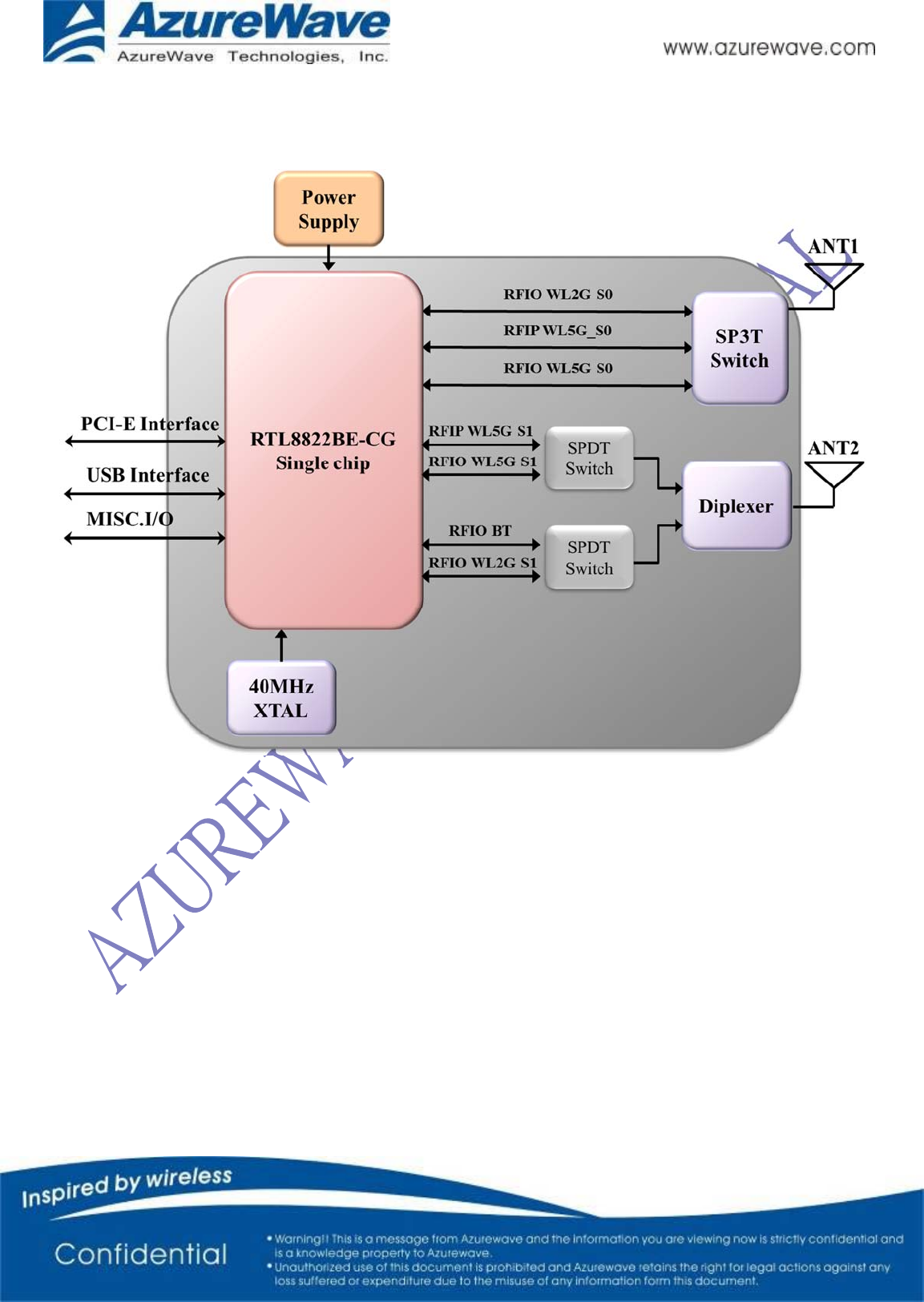
3. Block Diagram
A simplified block diagram of the AW-CM308NF module is depicted in the figure below.
8
4. Specifications Table
Model Name AW-CM308NF
Product Description Wireless LAN & Bluetooth Combo M.2 Module
WLAN Standard IEEE 802.11 a/b/g/n/ac
Bluetooth Standard Bluetooth 2.1+Enhanced Data Rate (EDR) + BT4.2
Major Chipset RTL8822BE-CG
Host Interface Wi-Fi : PCI-E , Bluetooth : USB
Antenna
I-PEX MHF4 Connector Receptacle (20449)
ANT1 : WiFi TX/RX
ANT2 : WiFi/Bluetooth Tx/Rx
Dimension 12mm x16mm x 1.7mm
(Tolerance remarked in mechanical drawing)
Wi-Fi SVID/SSID 1A3B / 3081
BT VID/PID 13D3 / 3536
Weight 0.0006 kg
Operating Conditions
Voltage power supply for host:3.3V
Operating temperature 0~70 ℃
Storage temperature -30~85 ℃
Electrical Specifications
Frequency Range
WLAN:
2.4 GHz : 2.412 ~ 2.484 GHz
5 GHz: 4.915 ~5.925Ghz
Bluetooth:
2402~2480MHz
Modulation
DSSS, OFDM, DBPSK, DQPSK, CCK, 16-QAM, 64-QAM, 256-
QAM for WLAN
GFSK (1Mbps), Π/4 DQPSK (2Mbps) and 8DPSK (3Mbps) for
Bluetooth
9
Output Power
WLAN:
802.11b : 16 +/-2dBm (11Mbps)
802.11g : 14 +/-2dBm (54Mbps)
802.11n @2.4GHz : 13 +/-2dBm (HT20 MCS7)
802.11n @2.4GHz : 13 +/-2dBm (HT40 MCS7)
802.11a @5GHz : 13 +/-2dBm (54Mbps)
802.11n @5GHz : 12 +/-2dBm (HT20 MCS7)
802.11n @5GHz : 12 +/-2dBm (HT40 MCS7)
802.11ac @5GHz : 10 +/-2dBm (HT80 MCS9)
BT: 0 ~ 6 dBm
Receive Sensitivity
WLAN :
802.11b : -82dBm (11Mbps)
802.11g : -71dBm (54Mbps)
802.11n @2.4GHz : -68dBm (HT20 MCS7)
802.11n @2.4GHz : -66dBm (HT40 MCS7)
802.11a @5GHz : -69dBm (54Mbps)
802.11n @5GHz : -67dBm (HT20 MCS7)
802.11n @5GHz : -64dBm (HT40 MCS7)
802.11ac @5GHz : -54dBm (HT80 MCS9)
BT : BER < 0.1%
(
Anritsu 8852B Tx -70 Bm
)
Data Rates
WLAN
802.11b: 1, 2, 5.5, 11Mbps
802.11a/g: 6, 9, 12, 18, 24, 36, 48, 54Mbps
802.11n: up to 150Mbps-single
802.11n: up to 300Mbps-2x2 MIMO
802.11ac:up to 192.6Mbps (20MHz channel)
802.11ac:up to 400Mbps (40MHz channel)
802.11ac:up to 866.7Mbps (80MHz channel)
Bluetooth
Bluetooth 2.1+EDR data rates of 1,2, and 3Mbps
Security
WAPI
WEP 64-bit and 128-bit encryption with H/W TKIP
processing
WPA/WPA2 (Wi-Fi Protected Access)
AES-CCMP hardware implementation as part of 802.11i
security standard
Operating System
Compatibility Refer to Realtek/ RTL8822BE-CG regulatory list
ESDSpecifications
ESD rating HBM >1.5KV
CDM > 400V
10
5. Electrical Characteristics
5.1 Recommended DC Operating Conditions
Symbol Parameter Minimum Typical Maximum Unit
Vdd33 I/O voltage 3.0 3.3 3.6 V
5.2 Digital IO Pin DC Characteristics
Table 1. 3.3V IO DC Characteristics
Symbol Parameter Minimum Typical Maximum Unit
VIH Input high voltage 2.0 3.3 3.6 V
VIL Input low voltage -- 0 0.9 V
VOH Output high voltage 2.97 -- 3.3 V
VOL Output low voltage 0 -- 0.33 V
Table 2. 1.8V IO DC Characteristics
Symbol Parameter Minimum Typical Maximum Unit
VIH Input high voltage 1.7 1.8 2.0 V
VIL Input low voltage - 0 0.8 V
VOH Output high voltage 1.62 - 1.8 V
VOL Output low voltage 0 - 0.18 V
5.3 LED mode behavior
State Definition Interpretation
OFF The LED is emitting no
light.
Radio is incapable of transmitting.
This state is indicated when the card is not powered, the
W_Disable# signal is asserted to disable the radio, or when the
radio is disabled by software.
ON The LED is emitting
light.
Radio is capable of transmitting.
The LED should remain ON even if the radio is bit actually
transmitting. For example, the LED remains ON during
temporary radio disablements performed by the Mini Card of its
own volition to do scanning, switching radios/bands, power-
management, etc.
If the card is in a state wherein it is possible that radio can begin
transmitting without the system user performing any action, this
LED should remain ON.
11
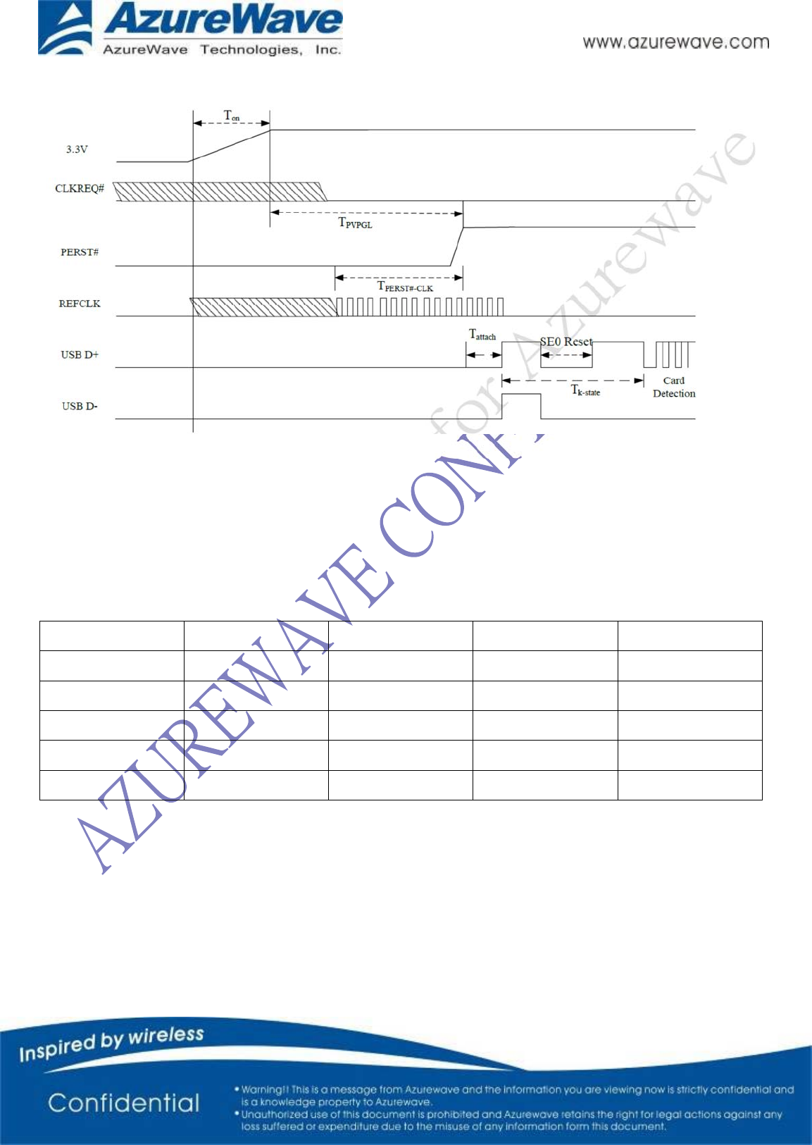
5.4 PCIe Bus during power on sequence
T
on
: The main power ramp up duration
T
PVPGL
: Power valid PERST# input inactive
T
PERST#-CLK
: Reference clock stable before PERST# inactive
T
attach
: USB attach state
T
k-state
: the duration from resister attached to USB host starting card detection procedure.
If use the 1.8V VIO, we suggest timing range 100us ~ 3ms after 3.3V power supply.
The typical timing range
Symbol Unit Min Typical Max
T
on
ms 1 1.5 5
T
PVPGL
ms --
T
PERST#-CLK
us 100 --
T
attach
ms 2 7 15
T
k-state
ms 50 250 --
12
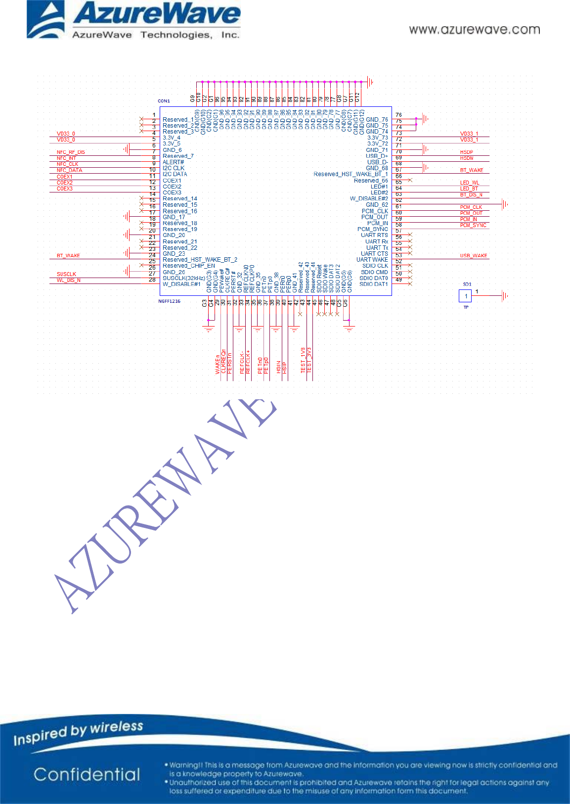
6. Pin Definition
Pin Description (1216 NGFF)
Pin No. Definition Basic Description Type Voltage
1 NC Floating Pin, No connect to anything. Floating
2 NC Floating Pin, No connect to anything. Floating
3 NC Floating Pin, No connect to anything. Floating
4 3.3V 3.3V power supply VCC 3.3V
5 3.3V 3.3V power supply VCC 3.3V
6 GND Ground. GND
7 RESERVED Floating Pin, No connect to anything. Floating
8 RESERVED Floating Pin, No connect to anything. Floating
9 RESERVED Floating Pin, No connect to anything. Floating
10 RESERVED Floating Pin, No connect to anything. Floating
11 RESERVED Please don't connect to this pin. N/A
12 RESERVED Please don't connect to this pin. N/A
13 RESERVED Please don't connect to this pin. N/A
14 RESERVED Floating Pin, No connect to anything. Floating
15 RESERVED Floating Pin, No connect to anything. Floating
16 RESERVED Floating Pin, No connect to anything. Floating
17 GND Ground. GND
18 RESERVED Floating Pin, No connect to anything. Floating
19 RESERVED Floating Pin, No connect to anything. Floating
20 GND Ground. GND
21 RESERVED Floating Pin, No connect to anything. Floating
22 RESERVED Floating Pin, No connect to anything. Floating
23 GND Ground. GND
24 BT_WAKE Host wake BT. No function, please don't connect to
this pin. N/A
25 RESERVED Floating Pin, No connect to anything. Floating
26 GND Ground. GND
27 SUSCLK Please don't connect to this pin. Floating
28 W_DISABLE1# Turn off WLAN RF analog and front–end. Active low.
This pin is controlled by system. (IC internal pull up) IN VIO
29 PEWAKE#
Open Drain active Low signal. This signal is used to
request that the system return from a
sleep/suspended state to service a function initiated
wake event.
OUT 3.3V
30 CLKREQ# Reference clock request. I/O 3.3V
13
31 PERST# PCI Express reset with weak pull–down. IN 3.3V
32 GND Ground. GND
33 REFCLKn0 Differential reference clock. IN
34 REFCLKp0 Differential reference clock. IN
35 GND Ground. GND
36 PETn0 Differential transmit. OUT
37 PETp0 Differential transmit. OUT
38 GND Ground. GND
39 PERn0 Differential receive. IN
40 PERp0 Differential receive. IN
41 GND Ground. GND
42 RESERVED Floating Pin, No connect to anything. Floating
43 VIO (TEST_1V8) VDDIO 1.8V/ 3.3V VCC VIO
44 TEST_3V3 For test pin. N/A
45 NC Floating Pin, No connect to anything. Floating
46 NC Floating Pin, No connect to anything. Floating
47 NC Floating Pin, No connect to anything. Floating
48 NC Floating Pin, No connect to anything. Floating
49 NC Floating Pin, No connect to anything. Floating
50 NC Floating Pin, No connect to anything. Floating
51 NC Floating Pin, No connect to anything. Floating
52 NC Floating Pin, No connect to anything. Floating
53 USB_WAKE BT wake host. No function, please don't connect to
this pin. N/A
54 NC Floating Pin, No connect to anything. Floating
55 NC Floating Pin, No connect to anything. Floating
56 NC Floating Pin, No connect to anything. Floating
57 NC Floating Pin, No connect to anything. Floating
58 PCM_SYNC PCM synchronous data output, connected to PCM_IN
on the host. Out
59 PCM_IN PCM Clock I/O
60 PCM_OUT PCM synchronous data input, connected to
PCM_OUT on the host. IN
61 PCM_CLK PCM synchronous data SYNC I/O
62 GND Ground. GND
63 BT_DISABLE BT disable control. This pin is controlled by system.
(IC internal pull up) IN VIO
64 LED2# BT led function OUT
65 LED1# WL led function OUT

14
66 RESERVED Floating Pin, No connect to anything. Floating
67 BT_WAKE Host wake BT. No function, please don't connect to
this pin. N/A
68 GND Ground. GND
69 USB_D- DM_USB_BT I/O
70 USB_D+ DP_USB_BT I/O
71 GND Ground. GND
72 3.3V 3.3V power supply VCC 3.3V
73 3.3V 3.3V power supply VCC 3.3V
74 GND Ground. GND
75 GND Ground. GND
76 GND Ground. GND
77 GND Ground. GND
78 GND Ground. GND
79 GND Ground. GND
80 GND Ground. GND
81 GND Ground. GND
82 GND Ground. GND
83 GND Ground. GND
84 GND Ground. GND
85 GND Ground. GND
86 GND Ground. GND
87 GND Ground. GND
88 GND Ground. GND
89 GND Ground. GND
90 GND Ground. GND
91 GND Ground. GND
92 GND Ground. GND
93 GND Ground. GND
94 GND Ground. GND
95 GND Ground. GND
96 GND Ground. GND
G1 G1 Ground. GND
G2 G2 Ground. GND
G3 G3 Ground. GND
G4 G4 Ground. GND
G5 G5 Ground. GND
G6 G6 Ground. GND
15
G7 G7 Ground. GND
G8 G8 Ground. GND
G9 G9 Ground. GND
G10 G10 Ground. GND
G11 G11 Ground. GND
G12 G12 Ground. GND
16
7 Schematics
17
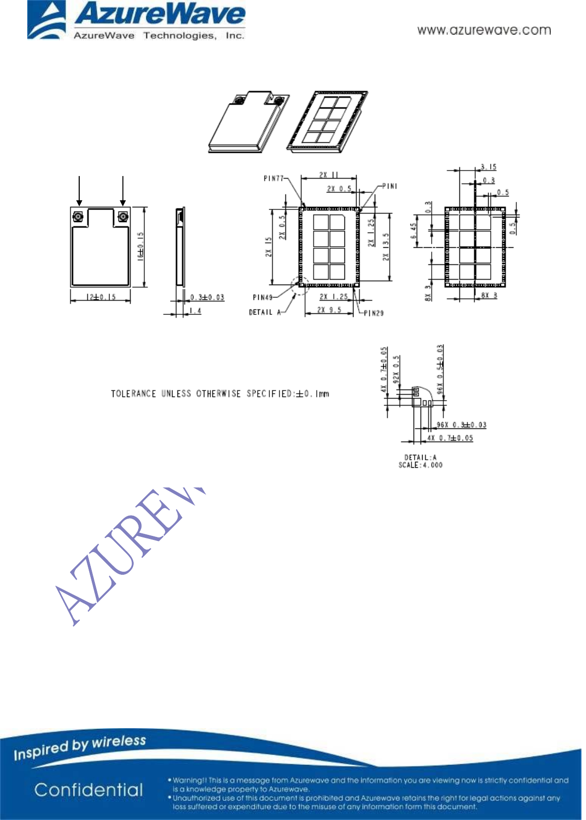
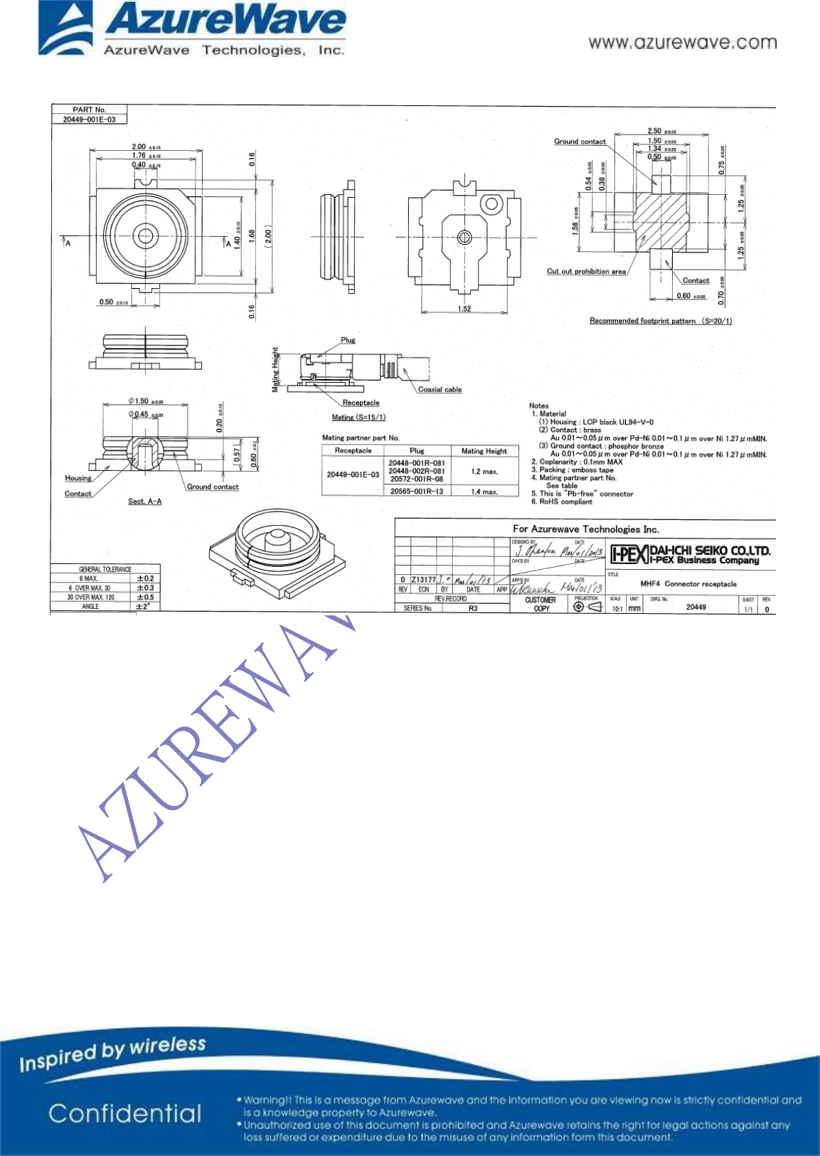
8 Mechanical Information
Main (ANT1) Aux (ANT2)
18
Antenna Connector Drawing

19
FEDERAL COMMUNICATION COMMISSION INTERFERENCE STATEMENT
This equipment has been tested and found to comply with the limits for a Class B digital device, pursuant to Part 15
of the FCC Rules. These limits are designed to provide reasonable protection against harmful interference in a
residential installation.
This equipment generates, uses and can radiate radio frequency energy and, if not installed and used in
accordance with the instructions, may cause harmful interference to radio communications. However, there is no
guarantee that interference will not occur in a particular installation. If this equipment does cause harmful
interference to radio or television reception, which can be determined by turning the equipment off and on, the user
is encouraged to try to correct the interference by one of the following measures:
. Reorient or relocate the receiving antenna.
. Increase the separation between the equipment and receiver.
. Connect the equipment into an outlet on a circuit different from that to which the receiver is connected.
. Consult the dealer or an experienced radio/TV technician for help.
FCC Caution: To assure continued compliance, any changes or modifications not expressly approved by the party
responsible for compliance could void the user's authority to operate this equipment. (Example - use only shielded
interface cables when connecting to computer or peripheral devices).
End Product Labeling
This transmitter module is authorized only for use in devices where the antenna may be installed such that 20 cm
may be maintained between the antenna and users. The final end product must be labeled in visible area with the
following: “Contains FCC ID: TLZ-CM308NF”
”
End Product Manual Information
The user manual for end users must include the following information in a prominent location “IMPORTANT NOTE:
To comply with FCC RF exposure compliance requirements, the antenna used for this transmitter must be installed
to provide a separation distance of at least 20cm from all persons and must not be colocated or operating in
conjunction with any other antenna or transmitter.” This device complies with part 15 of the FCC rules. Operation
is subject to the following two conditions (1) This device may not cause harmful interference and (2) This device
must accept any interference received, including interference that may cause undesired operation.
IMPORTANT NOTE: In the event that these conditions can not be met (for example certain laptop configurations
or colocation with another transmitter), then the FCC authorization is no longer considered valid and the FCC ID
can not be used on the final product. In these circumstances, the OEM integrator will be responsible for
reevaluating the end product (including the transmitter) and obtaining a separate FCC authorization. This device
is intended only for OEM integrators under the following conditions: The antenna must be installed such that 20 cm
is maintained between the antenna and users. As long as a condition above is met, further transmitter test will not
be required. However, the OEM integrator is still responsible for testing their end product for any additional
compliance requirements required with this module installed (for example, digital device emissions, PC peripheral
requirements, etc.).

20
NCC警語
「依據低功率電波輻射性電機管理辦法」
第十二條經型式認證合格之低功率射頻電機,非經許可,公司、商號或使用者
均不得擅自變更頻率、加大功率或變更原設計之特性及功能。
第十四條 低功率射頻電機之使用不得影響飛航安全及干擾合法通信;經發現有
干擾現象時,應立即停用,並改善至無干擾時方得繼續使用。
前項合法通信,指依電信法規定作業之無線電通信。低功率射頻電機須忍受合
法通信或工業、科學及醫療用電波輻射性電機設備之干擾。」
*應避免影響附近雷達系統之操作。
*高增益指向性天線只得應用於固定式點對點系統。
本模組於取得認證後,將依規定於模組本體標示審驗合格標籤,並要求平台廠
商於平台上標示「本產品內含射頻模組 XXXyyyLPDzzzz-x」
電磁波曝MPE標準值1mW/cm2,送測產品實________mW/cm2。