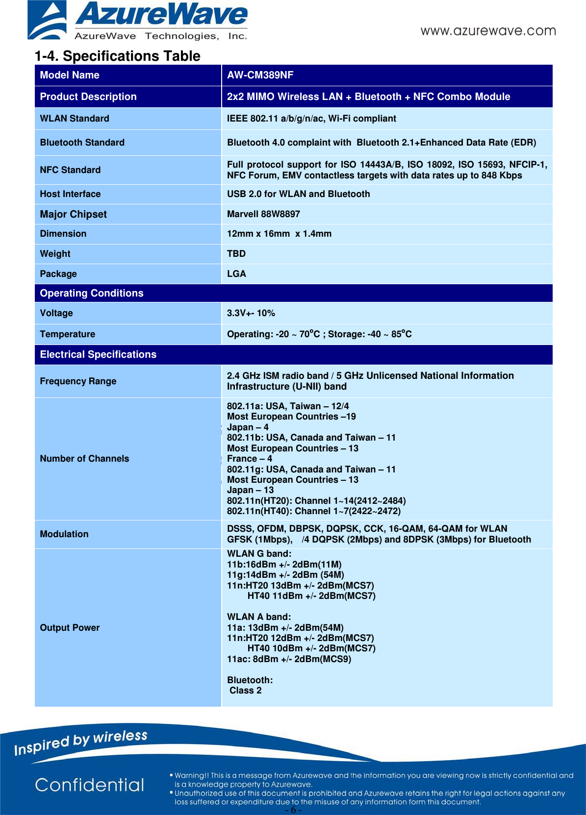
AzureWave Technologies CM389NF IEEE 802.11 2X2 MIMO a/b/g/n/ac Wireless LAN + Bluetooth + NFC NGFF Module User Manual AW AH691A
AzureWave Technologies, Inc. IEEE 802.11 2X2 MIMO a/b/g/n/ac Wireless LAN + Bluetooth + NFC NGFF Module AW AH691A
Contents
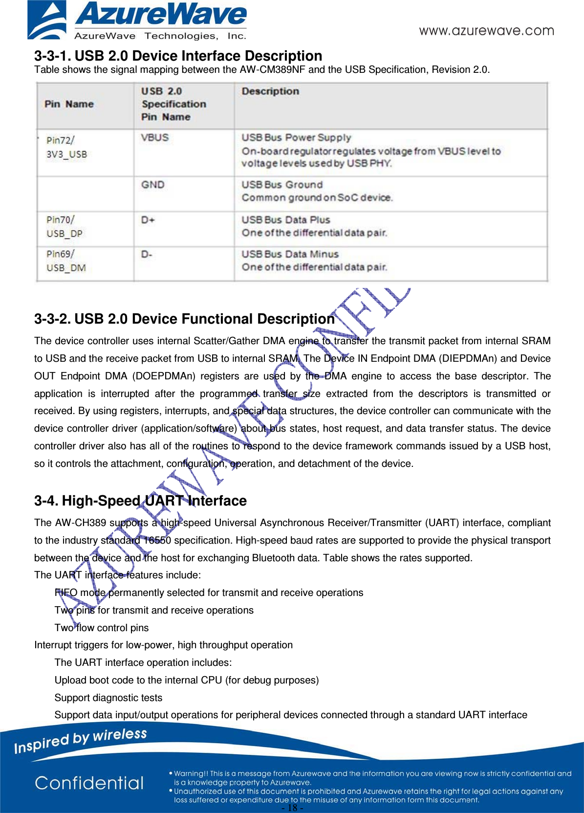
User Manual.pdf
![- 4 - 1-2. Block Diagram Note: Interface supports and combinations as shown below: Scenario WLAN BT/NFC BT_AMPS Firmware Download I/F Firmware Download Mode Configuration* 1 SDIO SDIO SDIO SDIO Serial CON[3:0]=b'0111 2 SDIO SDIO -- SDIO Serial CON[3:0]=b'0001 3 SDIO UART SDIO SDIO or UART Serial CON[3:0]=b'1101 4 SDIO UART SDIO SDIO + UART Parallel CON[3:0]=b'0010 5 SDIO UART -- SDIO or UART Serial CON[3:0]=b'0100 6 USB USB USB USB Serial CON[3:0]=b'0110 7 USB UART USB USB or UART Serial CON[3:0]=b'1010 8 USB UART -- USB + UART Parallel CON[3:0]=b'1000 9 PCIe UART -- PCIe + UART Parallel CON[3:0]=b'1111 10 PCIe UART -- PCIe or UART Serial CON[3:0]=b'1100 11 PCIe USB USB PCIe Serial CON[3:0]=b'1110](https://usermanual.wiki/AzureWave-Technologies/CM389NF.User-Manual-pdf/User-Guide-2320262-Page-4.png)
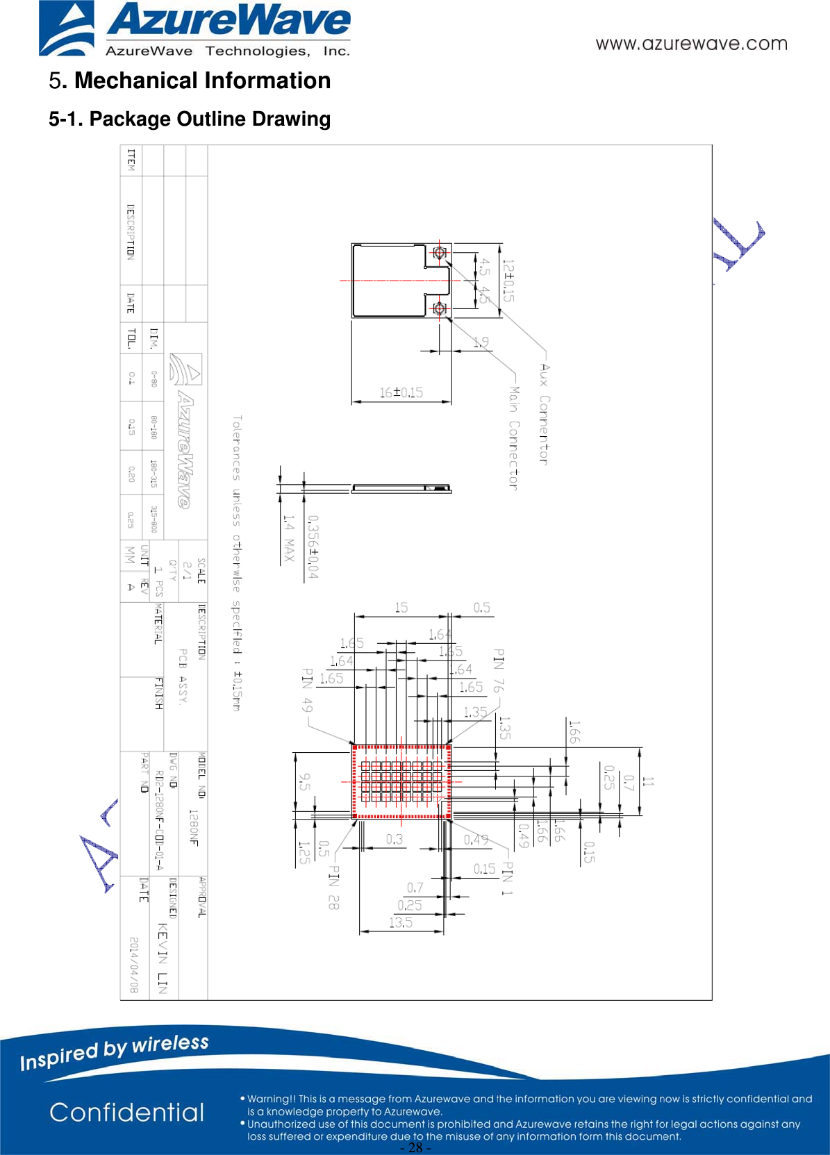
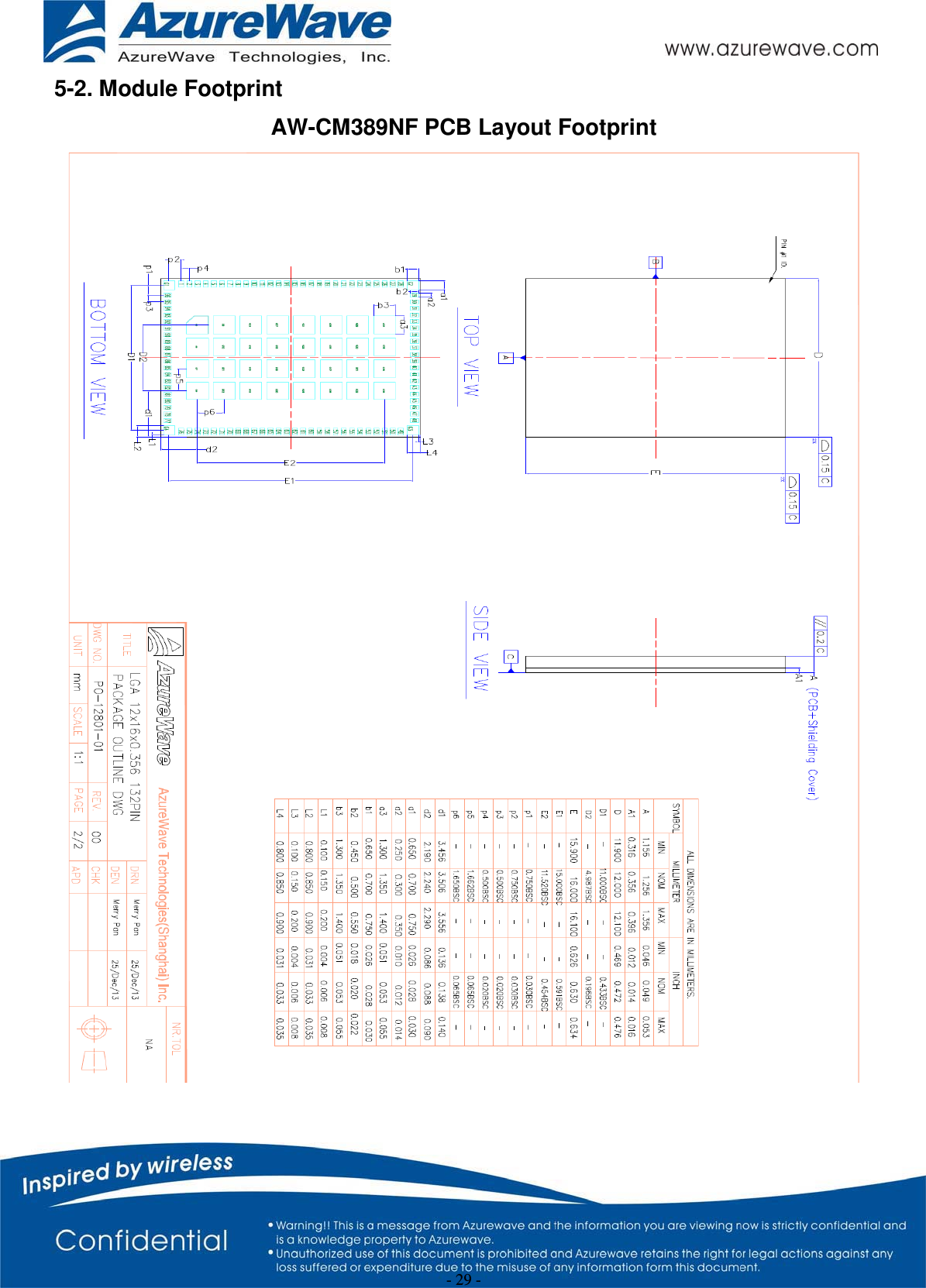
![- 5 - *Configuration pins: Configuration Pin No Pin Name CON[3] 13 CONFIG_HOST[3] CON[2] 10 CONFIG_HOST[2] CON[1] 9 CONFIG_HOST[1] CON[0] 8 CONFIG_HOST[0] 1-3. Key feature: Small footprint: 12mm(L) x 16mm(W) x 1.4 mm(H) SDIO3.0, G-SPI, USB interfaces support for WLAN High speed UART,PCM/Inter-IC Sound(I2S) and SDIO3.0, USB for Bluetooth Bluetooth 4.0 complaint with Bluetooth 2.1 + Enhanced Data Rate (EDR) Audio Codec interface support Cellular phone co-existence support Multiple power saving modes for low power consumption IEEE 802.11i for advanced security Quality of Service (QoS) support for multimedia applications Drip-in WLAN Linux drivers are Android ready and validated on Android based systems. Support for Linux kernel versions up to 2.6.32. Support for BlueZ v4.47 Bluetooth profiles stack used in Android Éclair Simultaneous AP-STA Support China WAPI Lead-free design](https://usermanual.wiki/AzureWave-Technologies/CM389NF.User-Manual-pdf/User-Guide-2320262-Page-5.png)
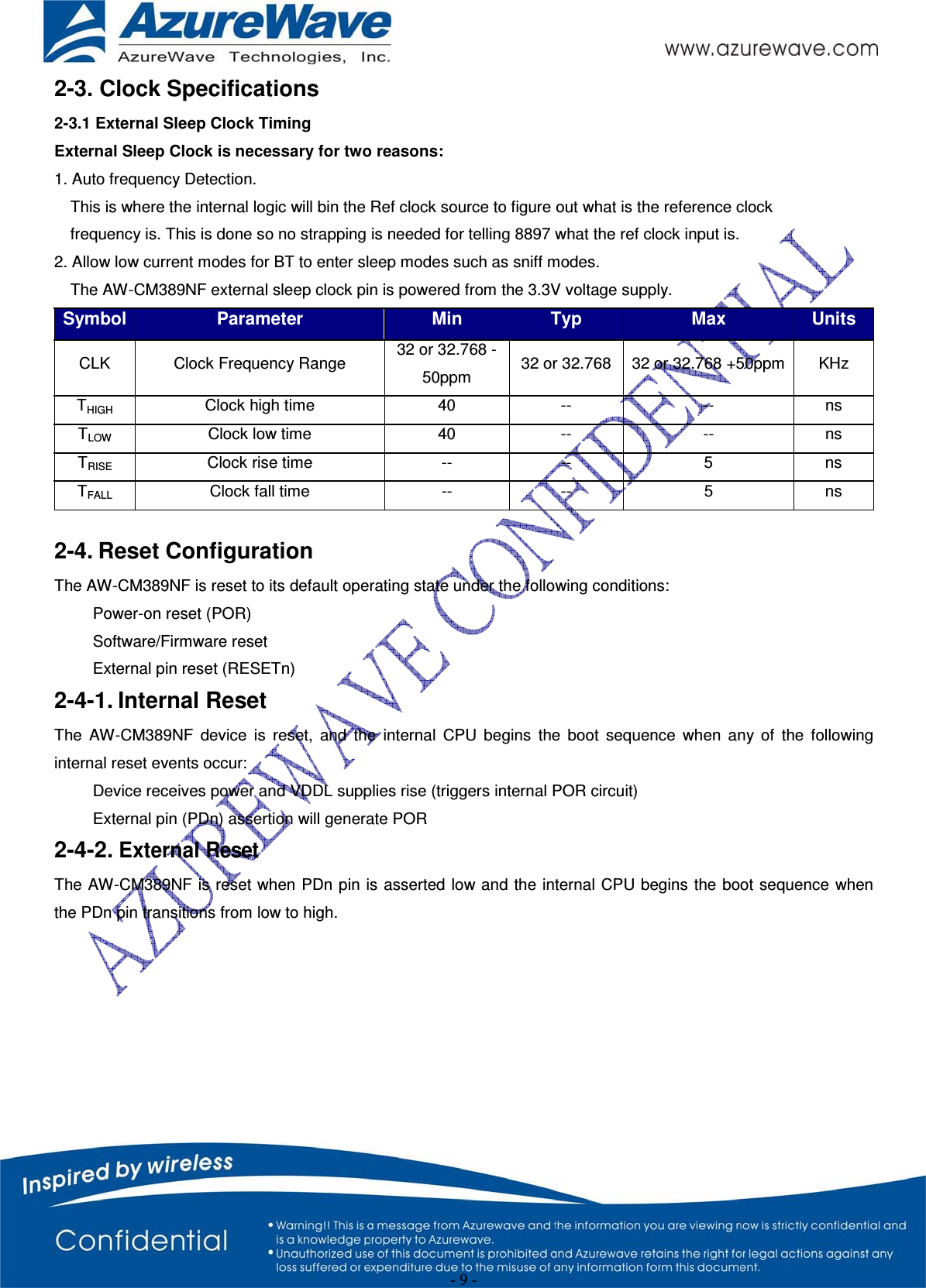
![- 8 - 2. Electrical Characteristic 2-1. Absolute Maximum Ratings Symbol Parameter Condition Min Typ Max UnitsPin73/ VIO Host I/O power supply -- -- -- -- -- -- 1.8 2.5 3.3 2.2 3.0 4.0 V Pin44/ VIO_SD SDIO power supply -- -- -- -- 1.8 3.3 2.2 4.0 V Pin5/ 3V3_VBAT LDO VBAT input -- -- 3.3 5.0 V Pin72/ 3V3_USB LDO USB VBAT input -- -- 3.3 4.0 V Pin4/ 3V3_RF LDO RF VBAT input -- -- 3.3 4.0 V 2-2. Recommended Operating Conditions Symbol Parameter Condition Min Typ Max UnitsPin73/ VIO 1.8V/2.5V/3.3V digital I/O power supply -- -- -- 1.62 2.25 2.97 1.8 2.5 3.3 1.98 2.75 3.63 V Pin44/ VIO_SD 1.8V/3.3V digital I/O SDIO power supply -- -- 1.62 2.97 1.8 3.3 1.98 3.63 V Pin5/ 3V3_VBAT LDO VBAT input -- 2.7 3.3 5.0 V Pin72/ 3V3_USB LDO USB VBAT input -- 2.97 3.3 3.63 V Pin4/ 3V3_RF LDO RF VBAT input -- 2.97 3.3 3.63 V 2-2.1 The interface pins power supply The NFC interface pins are powered from the module’s chip LDO 1.8V voltage supply internal. The SDIO host interface pins are powered from the chip VIO_SD (pin 44) 1.8V/3.3V voltage supply. - SDIO Defauld Speed, High Speed Modes (3.3V) - SDR12, SDR25, SDR50 Modes (up to 100MHz) (1.8V) - SDR104 Mode (208MHz) (1.8V) The PCI Express host interface pins are powered from the module’s chip LDO 1.8V voltage supply internal. The USB2.0 host interface pins are powered from the 3V3_USB (pin 72) 3.3V voltage supply. The UART Tx and Rx pins are powered from the VIO (pin 73) voltage supply. The GPIO pins are powered from the VIO (pin 73) voltage supply (GPIO [9:8] from 3.3V voltage internal). The clocked serial pins are powered from the module’s chip LDO 1.8V voltage supply internal. The audio pins are powered from the chip VIO (pin 73) voltage supply.](https://usermanual.wiki/AzureWave-Technologies/CM389NF.User-Manual-pdf/User-Guide-2320262-Page-8.png)
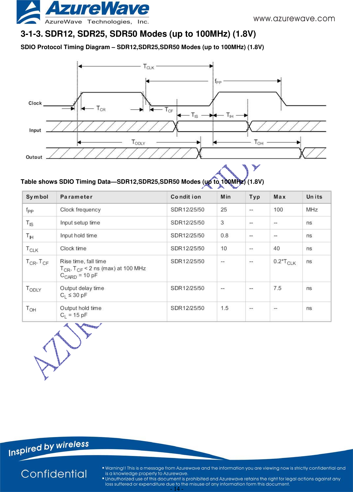
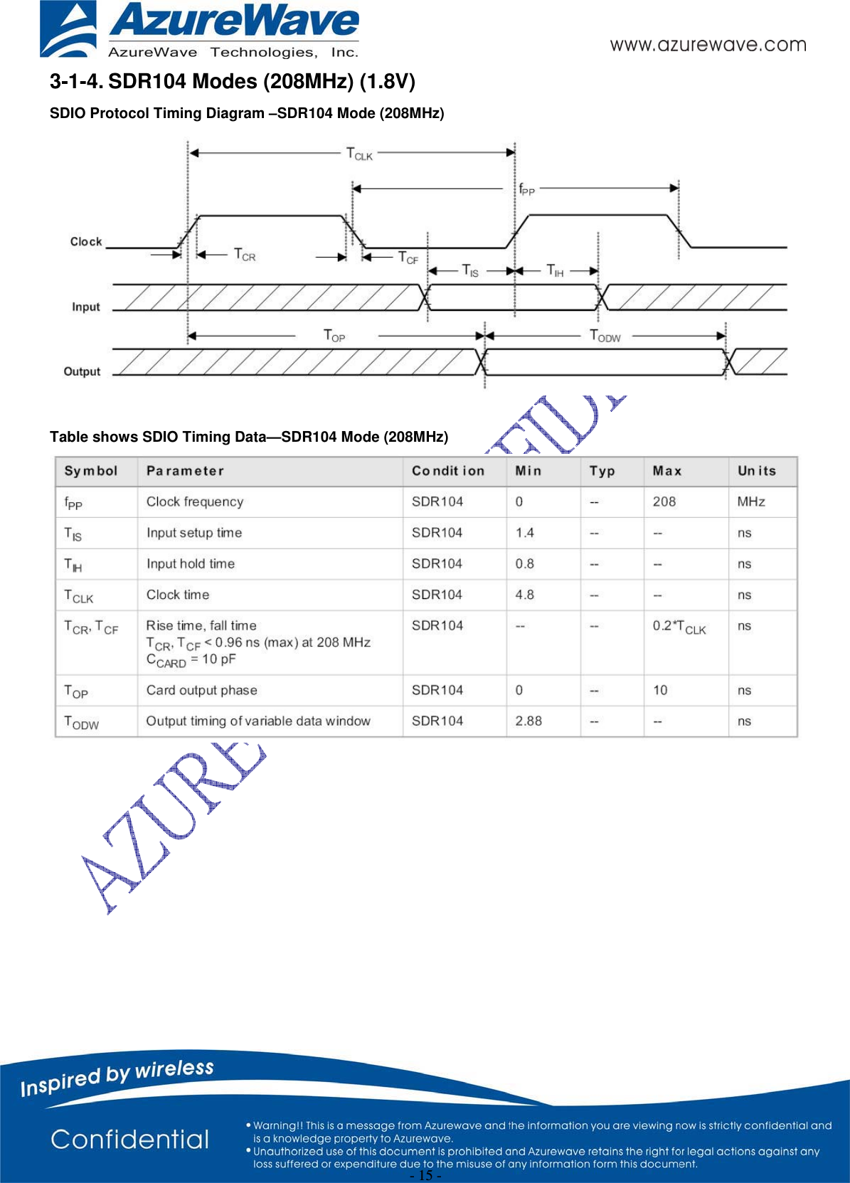
![- 11 - 3. Host Interfaces 3-1. SDIO Interface The AW-CM389NF supports a SDIO device interface that conforms to the industry standard SDIO Full-Speed card specification and allows a host controller using the SDIO bus protocol to access the Wireless module device. The AW-CM389NF acts as the device on the SDIO bus. The host unit can access registers of the SDIO interface directly and can access shared memory in the device through the use of BARs and a DMA engine. The SDIO device interface main features include: Supports SDIO 3.0 Standard On-chip memory used for CIS Supports SPI, 1-bit SDIO, and 4-bit SDIO transfer modes Special interrupt register for information exchangeAllows card to interrupt host 3-1-1. SDIO Interface Signal Description Pin NameSignalNameTypeDescriptionSD_CLK CLK I/O SDIO 1-bit mode: Clock SDIO SPI mode: Clock SD_CMD CMD I/O SDIO 1-bit mode: Command line SDIO SPI mode: Data input SD_DAT[3] DAT3 I/O SDIO 4-bit mode: Data line bit [3] SDIO 1-bit mode: Not used SDIO SPI mode: Chip select (active low) SD_DAT[2] DAT2 I/O SDIO 4-bit mode: Data line bit [2] or Read Wait (optional) SDIO 1-bit mode: Read Wait (optional) SDIO SPII mode: Reserved SD_DAT[1] DAT1 I/O SDIO 4-bit mode: Data line bit [1] SDIO 1-bit mode: Interrupt SDIO SPI mode: Interrupt SD_DAT[0] DAT0 I/O SDIO 4-bit mode: Data line bit [0] SDIO 1-bit mode: Data line SDIO SPI mode: Data output](https://usermanual.wiki/AzureWave-Technologies/CM389NF.User-Manual-pdf/User-Guide-2320262-Page-11.png)
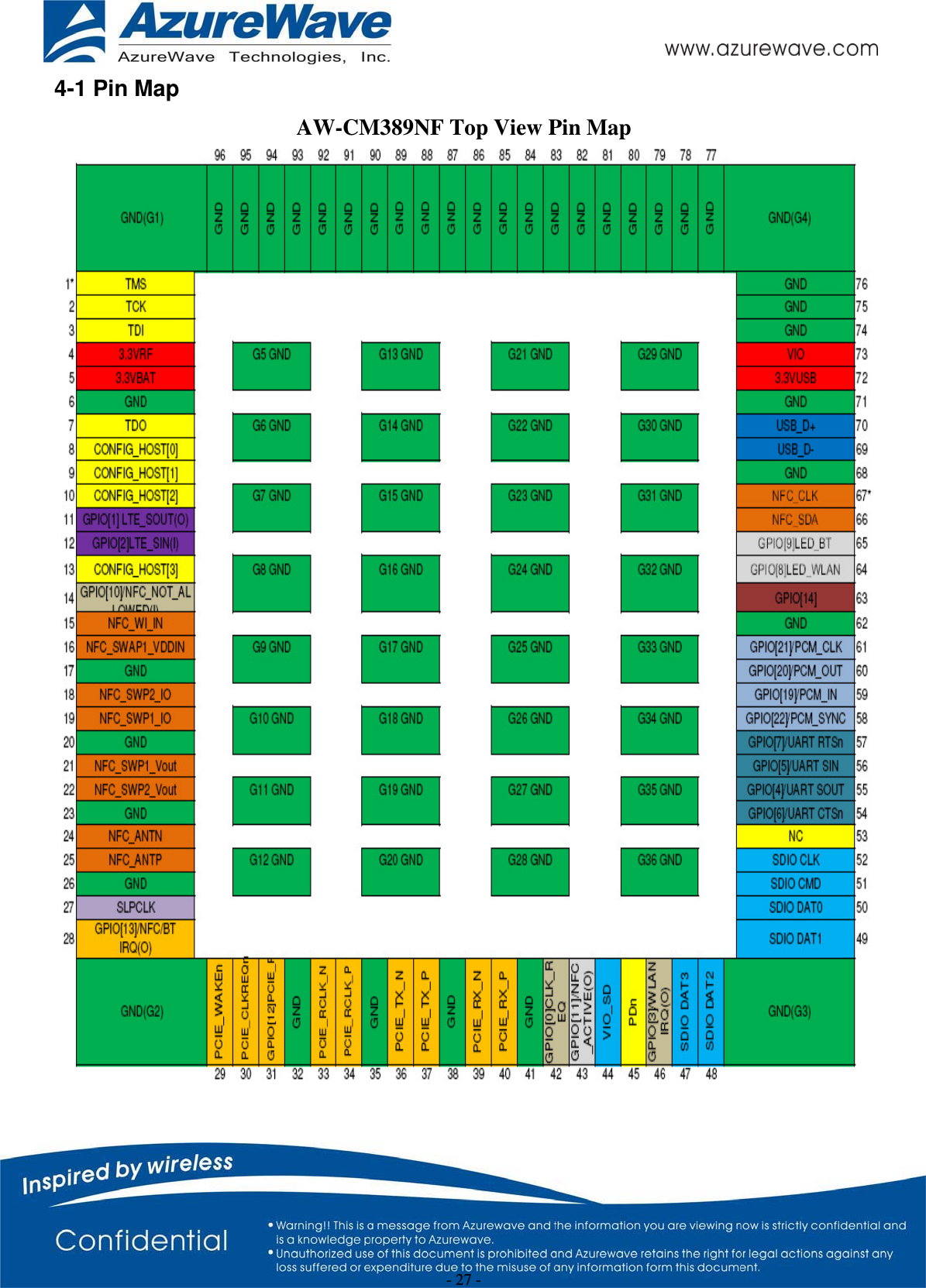
![- 22 - 4. Pin Definition Pin No Definition Basic Description Type 1 TMS JTAG controller select 2 TCK JTAG test clock 3 TDI JTAG test data(input) I 4 3V3_RF 3.3V Analog RF Power Supply I 5 3V3_VBAT 3.3V VBAT system power supply input I 6 GND System Ground Pin 7 TDO JTAG test data(output) O 8 CONFIG_HOST[0] Configuration: CONFIG_HOST[0] 9 CONFIG_HOST[1] Configuration: CONFIG_HOST[1] 10 CONFIG_HOST[2] Configuration: CONFIG_HOST[2]11 GPIO[1]/LTE_SOUT UART_LTE_SOUT (output) I 12 GPIO[2]/LTE_SIN UART_LTE_SIN (input) I 13 CONFIG_HOST[3] Configuration: CONFIG_HOST[3]14 GPIO[10]/NFC_NOT_ALLOWED(I) GPIO[10] (input/output) 15 NFC_WI_IN SE I/O for NFC-WI or DCLB, depending on the configuration I/O 16 NFC_SW1_VDDIN Supply from device to UICC thru integrated power switch CSP only I/O 17 GND System Ground Pin 18 NFC_SWP2_IO SE I/O for SWP, NFC-WI, or DCLB, depending on the configuration I/O 19 NFC_SWP1_IO UICC Single Wire Protocol I/O CSP only I/O 20 GND System Ground Pin 21 NFC_SWP1_Vout Supply to UICC from device thru integrated power switch CSP only. I/O 22 NFC_SWP2_Vout Supply from NFC to embedded SE CSP only. I/O 23 GND System Ground Pin 24 NFC_ANTN Antenna Interface, negative input/output I/O 25 NFC_ANTP Antenna Interface, positive input/output I/O 26 GND System Ground Pin 27 SLP_CLK Sleep Clock Input Used for WLAN and Bluetooth low-power modes. External sleep clock of 32.768 KHz must be used for auto reference clock calibration and for WLAN/Bluetooth low power operation. I](https://usermanual.wiki/AzureWave-Technologies/CM389NF.User-Manual-pdf/User-Guide-2320262-Page-22.png)
![- 23 - Pin No Definition Basic Description Type 28 GPIO[13]/NFC/BT IRQ(O) GPIO[13] (input/output) 29 PCIE_WAKEn PCIe wake signal (output) (active low) O 30 PCIE_CLKREQn PCIe clock request (input/output) (active low) I/O 31 GPIO[12]/PCIE_PERSTn PCIe host indication to reset the device (input) (active low) I 32 GND System Ground Pin 33 PCIE_RCLK_N PCI Express Differential Clock Input—Negative I 34 PCIE_RCLK_P PCI Express Differential Clock Input—Positive I 35 GND System Ground Pin 36 PCIE_TX_N PCI Express Transmit Data—Negative O 37 PCIE_TX_P PCI Express Transmit Data—Positive O 38 GND System Ground Pin 39 PCIE_RX_N PCI Express Receive Data—Negative I 40 PCIE_RX_P PCI Express Receive Data—Positive I 41 GND System Ground Pin 42 GPIO[0]/CLK_REQ GPIO[0] (input/output) O 43 GPIO[11]/NFC_ACTIVE(O) GPIO[11] (input/output) 44 VIO_SD 1.8V/3.3V Digital I/O SDIO Power Supply I 45 PDn Full Power Down (input) (active low) I 46 GPIO[3]/WLAN IRQ(O) GPIO[3] (input/output) I 47 SD_DAT[3] SDIO Data line Bit[3] I/O 48 SD_DAT[2] SDIO Data line Bit[2] I/O 49 SD_DAT[1] SDIO Data line Bit[1] I/O 50 SD_DAT[0] SDIO Data line Bit[0] I/O 51 SD_CMD SDIO Command/response (input/output) I/O 52 SD_CLK SDIO Clock input I 53 NC No Connect54 GPIO[6] UART_CTSn (input) I 55 GPIO[4] UART_SOUT (output) O 56 GPIO[5] UART_SIN (input) I 57 GPIO[7] UART_RTSn (output) O 58 GPIO[22]/PCM_SYNC GPIO[22] (input/output) I/O](https://usermanual.wiki/AzureWave-Technologies/CM389NF.User-Manual-pdf/User-Guide-2320262-Page-23.png)
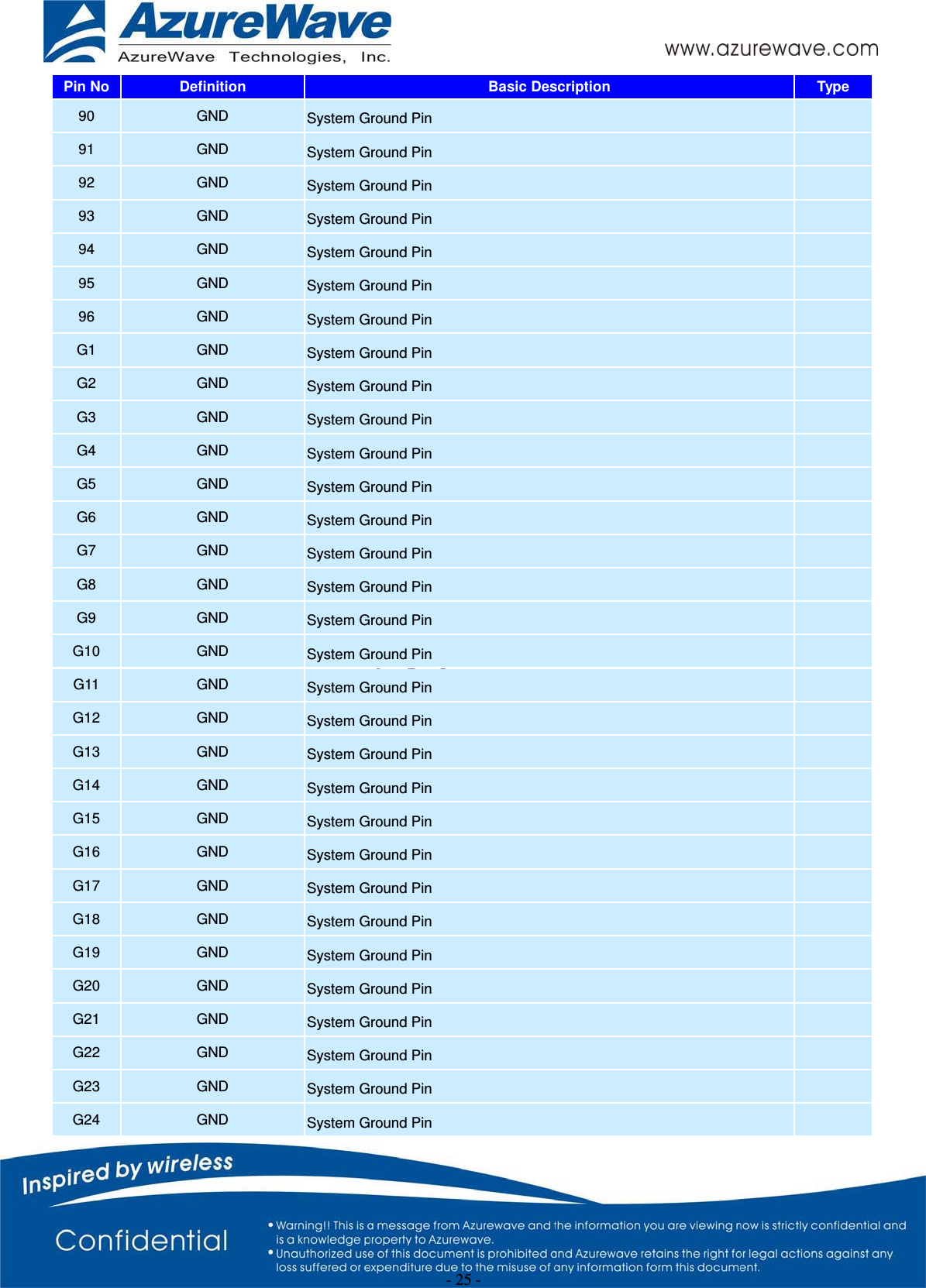
![- 24 - Pin No Definition Basic Description Type 59 GPIO[19]/PCM_IN GPIO[19] (input/output) I 60 GPIO[20]/PCM_OUT GPIO[20] (input/output) O 61 GPIO[21]/PCM_CLK GPIO[21] (input/output) I/O 62 GND System Ground Pin 63 GPIO[14] GPIO[14] (input/output) 64 GPIO[8]/WLAN_LED LED_OUT_WLAN (output) O 65 GPIO[9]/BT_LED LED_OUT_BT (output) O 66 NFC_SDA I/O for external EEPROM using 2-wire protocol CSP only. I/O 67 NFC_CLK Serial clock for external EEPROM using 2-wire protocol CSP only. I/O 68 GND System Ground Pin 69 USB_DM USB Serial Differential Data Negative I/O 70 USB_DP USB Serial Differential Data Positive I/O 71 GND System Ground Pin 72 3V3_USB 3.3V Power Supply I 73 VIO Digital I/O Power Supply I 74 GND System Ground Pin 75 GND System Ground Pin 76 GND System Ground Pin 77 GND System Ground Pin 78 GND System Ground Pin 79 GND System Ground Pin 80 GND System Ground Pin 81 GND System Ground Pin 82 GND System Ground Pin 83 GND System Ground Pin 84 GND System Ground Pin 85 GND System Ground Pin 86 GND System Ground Pin 87 GND System Ground Pin 88 GND System Ground Pin 89 GND System Ground Pin](https://usermanual.wiki/AzureWave-Technologies/CM389NF.User-Manual-pdf/User-Guide-2320262-Page-24.png)
![- 26 - Pin No Definition Basic Description Type G25 GND System Ground Pin G26 GND System Ground Pin G27 GND System Ground Pin G28 GND System Ground Pin G29 GND System Ground Pin G30 GND System Ground Pin G31 GND System Ground Pin G32 GND System Ground Pin G33 GND System Ground Pin G34 GND System Ground Pin G35 GND System Ground Pin G36 GND System Ground Pin Notes: 1. SDIO signals should have 50 ohm impedances. 2. For SDIO interface, 33ohm inline resistor may be needed to help with signal integrity. 3. For GPIO[8] ,it's internal pull up to VIO-RF(3.3V). 4. For GPIO[9] ,it's internal pull up to VIO-RF(3.3V). 5. For PDn pin ,please pull up resistor(51k ohm) to hots or VBAT(3V3). 6. For SDIO interface, the pull up value is between 10K to 100K ohm according to the SDIO v3.0 SPEC.7. PCIE Impedance targets: Single-ended Z of 60 ohms +- 15% . Differential Impedance of ~100 ohm +- 20%. 8. USB Impedance targets: D+/D- are differential and should have 90ohms impedance. 9. For NFC _SWP1_VDDIN ,please reserve a bypass capacitor(0.1 uF 0402) on the main board. 10. For GPIO[3] pin ,please pull up resistor(10k ohm) to VIO.](https://usermanual.wiki/AzureWave-Technologies/CM389NF.User-Manual-pdf/User-Guide-2320262-Page-26.png)