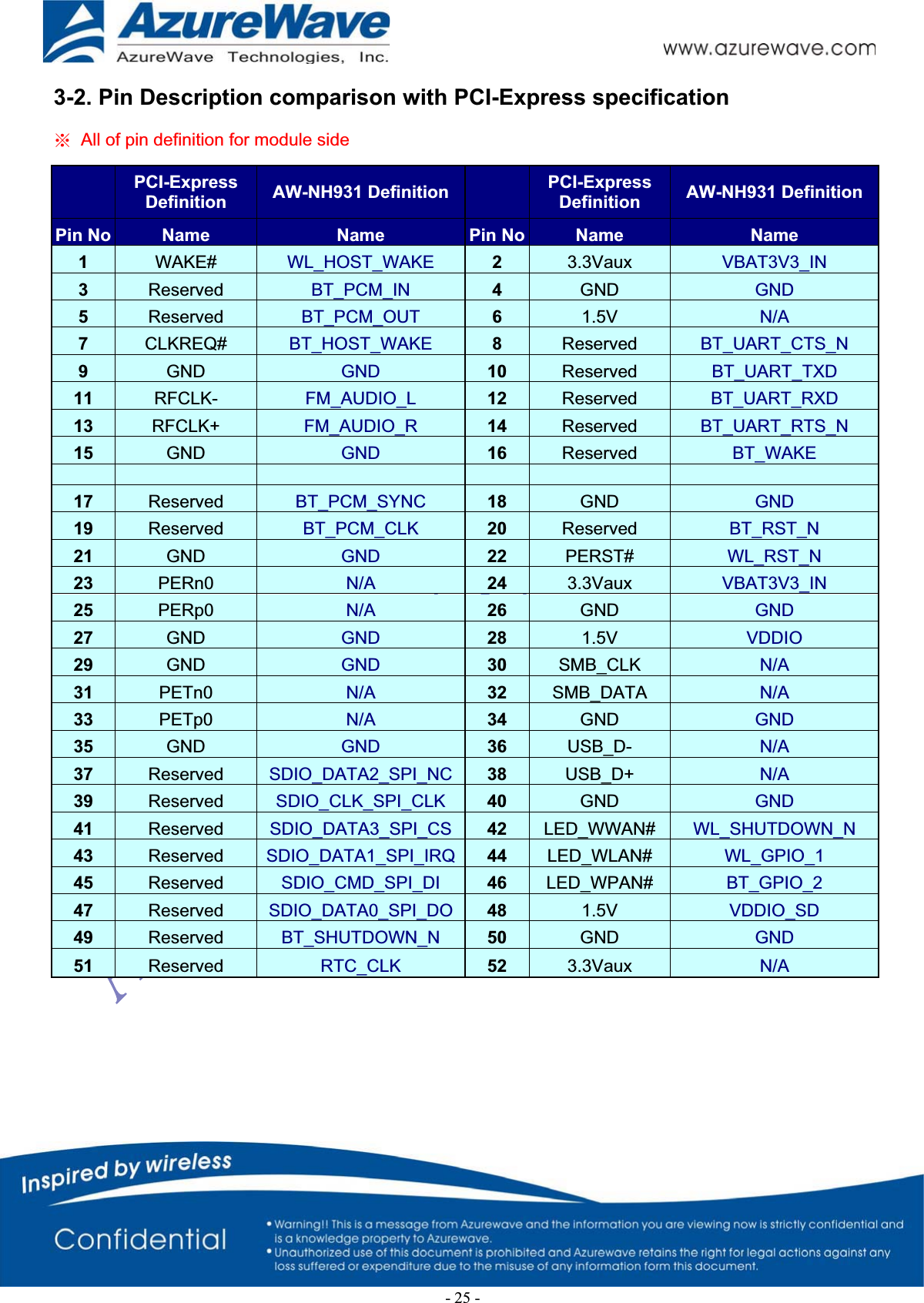
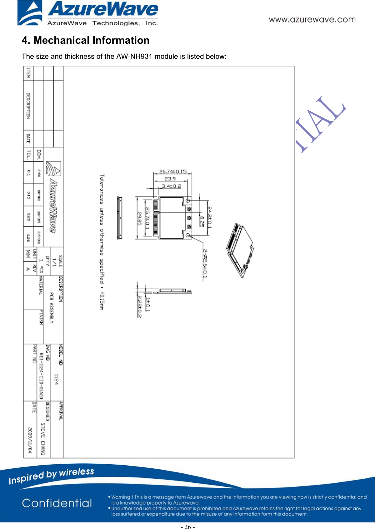
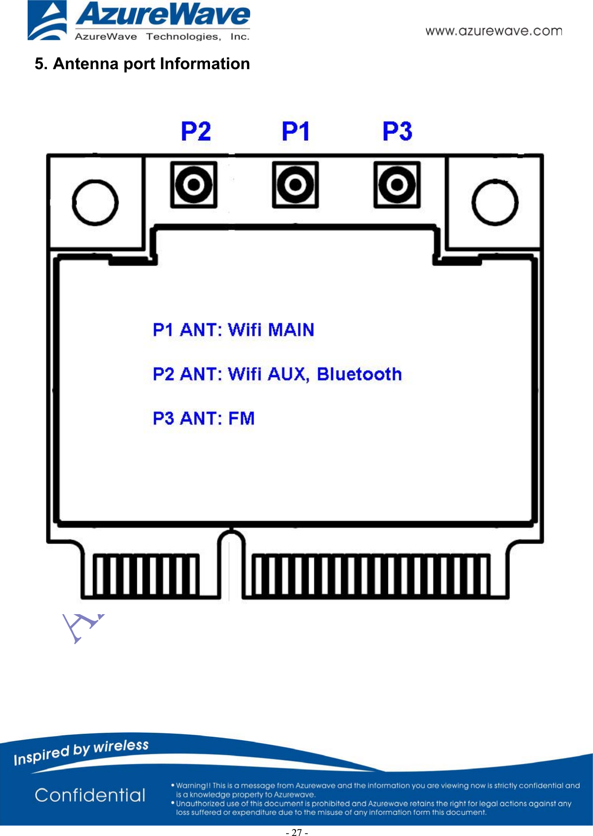
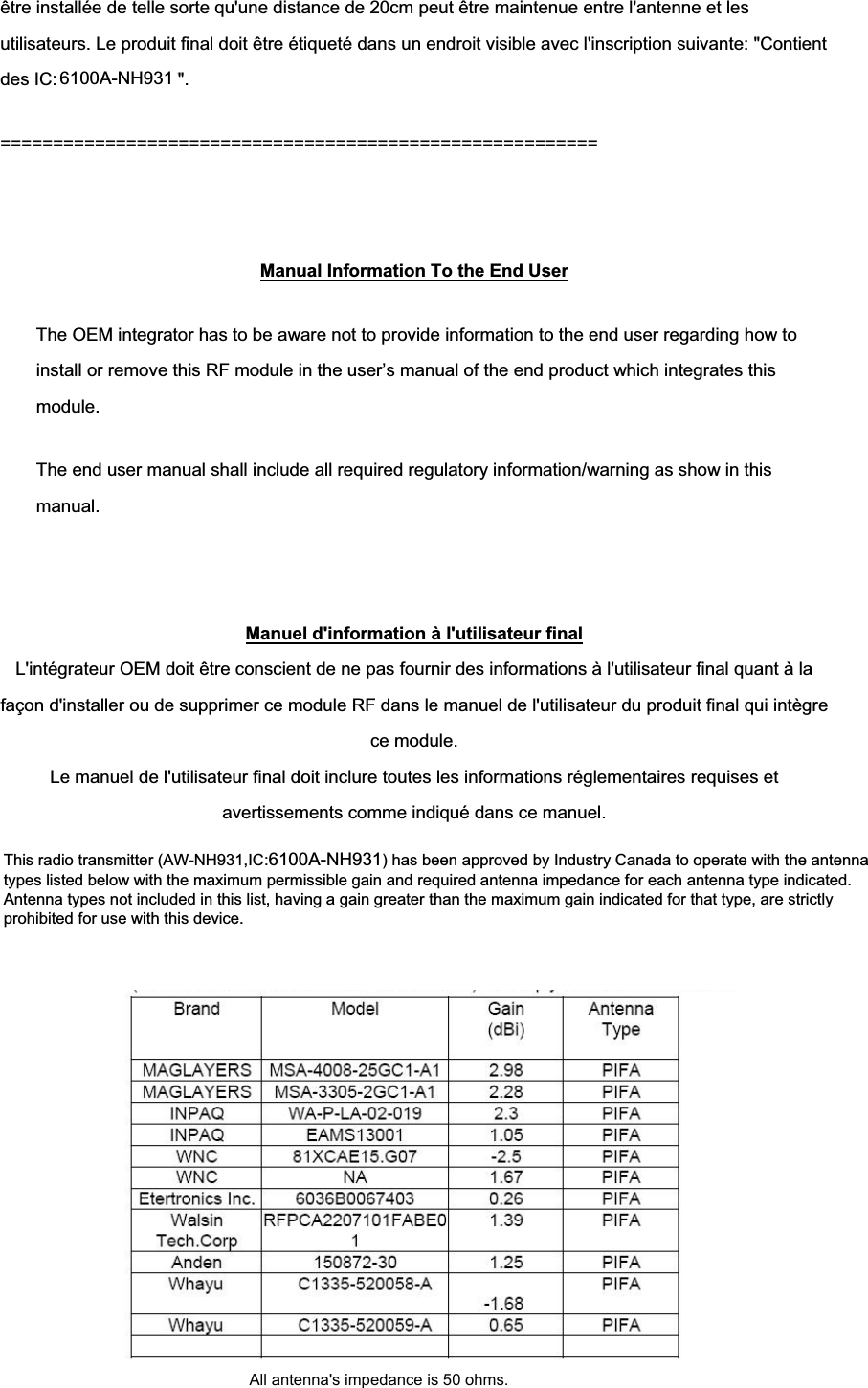
AzureWave Technologies NH931 IEEE 802.11b/g/n Wireless LAN, Bluetooth and FM Rx Combo Half Mini Card User Manual

AzureWave Technologies, Inc. IEEE 802.11b/g/n Wireless LAN, Bluetooth and FM Rx Combo Half Mini Card

Contents

User Manual

    AW-NH931  IEEE 802.11 b/g/n Wireless LAN, Bluetooth and FM Rx Combo Half Mini Card       Datasheet  Version 0.6         -1-
 Document release  Date Modification Initials ApprovedVersion 0.1  2010/10/11 Initial Version  N.C.  Chen  CE Huang Version 0.2  2010/12/3 Update Bluetooth output power spec. output power item on page 8 6.5dBm(Typ.) ÆClass 1.5 @ 7 dBm (±2 dBm) Class 2 @ 2 dBm (̈́ 2dBm) N.C.  Chen  CE Huang Version 0.3  2010/12/14 Update “Operating Temperature” on page 7Add 2-7. “Power-on sequence” on page 19 N.C.  Chen  CE Huang Version 0.4  2010/12/24Update  Section 5. “Antenna port information” on page 27 N.C.  Chen  CE Huang Version 0.5  2011/1/5  Update page 7 Electrical Specifications Number of Channels item on page 7 N.C.  Chen  CE Huang Version 0.6  2011/1/12 Update page7 Electrical Specifications Frequency Range description on page 7 2.4G/5GHz Æ 2.4GHz band N.C.  Chen  CE Huang -2-
Table of Contents 1. General Description 1-1.Product Overview and Functional Description 1-2. Key Features 1-3. Specifications Table2. Electrical Characteristic 2-1. Absolute Maximum Ratings 2-2. Recommended Operating Conditions 2-3. DC Characteristics for Host I/O 2-4. BT/FM Host Interface 2-5. SDIO Timing 2-6. LPO Clock (RTC_CLK) 2-7. Power-On sequence3. Pin Definition  3-1. Pin Description 3-2. Pin Description comparison with PCI-Express specification 4. Mechanical Information 5. Antenna port Information          -3-
1. General Description 1-1. Product Overview and Functional Description AzureWave Technologies, Inc. introduces the first IEEE 802.11b/g/n WLAN, Bluetooth and FM combo module - AW-NH931. The module is targeted to mobile devices including, Digital Still Cameras (DSCs), Portable Media Players (PMPs), and Gaming Devices, mobile phones which need small footprint package, low power consumption, multiple OS support. By using AW-NH931, the customers can easily enable the Wi-Fi, BT and FM embedded applications with the benefits of high design flexibility, short development cycle, and quick time-to-market. Compliance with the IEEE 802.11b/g/n standard, the AW-NH931 uses DSSS,OFDM,DBPSK,DQPSK,CCK and QAM baseband modulation technologies. A high level of integration and full implementation of the power management functions specified in the IEEE 802.11 standard minimize the system power requirements by using AW-NH931. In addition to the support of WPA/WPA2 (personal) and WEPencryption, the AW-NH931 also supports the IEEE 802.11i security standard through AES and TKIPacceleration hardware for faster data encryption. The AW-NH931 is also Cisco Compatible Extension (CCX)  certified. For the video, voice and multimedia applications the AW-NH931 support 802.11e Quality of Service (QoS).For Bluetooth operation, the AW-NH931 is Bluetooth 2.1+Enhanced Data Rate (EDR) compliant. TheAW-NH931 supports extended Synchronous Connections (eSCO), for enhanced voice quality by allowing for retransmission of dropped packets, and Adaptive Frequency Hopping (AFH) for reducing radio frequency interference. It provides easier to connect devices, lower power consumption and improved security.For FM receiver/transmitter, the AW-NH931 is 76-MHz to 108-MHz FM bands supported and supports the European Radio Data Systems (RDS) and the North American Radio Broadcast Data System (RBDS) modulations. The AW-NH931 supports standard interface SDIO v1.2 (4-bit and 1-bit) for WLAN, High-speed UARTinterface for BT/FM host controller interface, and PCM for BT audio data. The demodulated FM audio signal is available as line-level analog stereo output. AW-NH931 is suitable for multiple mobile processors for different applications. With the combo functions and the good performance, the AW-NH931 is the best solution for the consumer electronics and the laptops. -4-
1-2. Key Features General Integrates Broadcom solutions of BCM4329 WiFi/BT/FM SoC SDIO interfaces support for WLAN ECI—enhanced coexistence support, ability to coordinate BT SCO transmissions around WLAN receives High speed UART and PCM for Bluetooth  FM subsystem control through Bluetooth HCI interface Flexible Power Supply(2.3V~5.5V) Multiple power saving modes for low power consumption Lead-free /Halogen Free Design   WLAN Single - band 2.4 GHz 802.11 b/g/n Supports antenna diversity  Supports IEEE 802.11d, e, h,i, j,r,k,w Security–WEP, WPA/WPA2 (personal), AES (HW), TKIP (HW), CKIP (SW). WMM/WMM-PS/WMM-SA Proprietary protocol –CCXv2/CCXv3/CCXv4/CCXv5, WFAEC Integrated CPU with on-chip memory for a complete WLAN subsystem minimizing the need to wake up the applications processor  Bluetooth Fully supports Bluetooth Core Specification version 2.1 + EDR features Support BT3.0 Maximum UART baud rates up to 4 Mbps Multipoint operation with up to seven active slaves    -5-
FM 76-MHz to 108-MHz FM bands supported (US, Europe, and Japan) RDS and RBDS demodulator and decoder with filter and buffering functions Auto search and tuning modes FM line-level analog stereo output available By customer request    Block Diagram A simplified block diagram of the AW-NH931 module is depicted in the figure below.  VBAT 2.3~5.5V for internal PMU ANT 1  BCM4329SP3T BPF2.4 GHz WLAN Rx/BT Rx 2.4 GHz BT Tx XTALFM Rx AntennaFM RxRTC_Clk32.768KHz2.4 GHz WLAN TxUART for BT/FM SDIO for WLAN PCM for BT Analog Line-out/in for FM  SWANT 2-6-
1-3. Specifications Table *Specifications are subject to change without noticeModel Name  AW-NH931 Product Description  Wireless LAN &Bluetooth & FM WLAN Standard  IEEE 802.11b/g/n, Wi-Fi compliant Bluetooth Standard  Bluetooth 2.1+Enhanced Data Rate (EDR)  / BT3.0 Host Interface  SDIO for WLAN UART for Bluetooth and FM Audio Interface  Digital PCM for Bluetooth. Analog line level i/o for FM. Dimension  26.6 mm X 29.8 mm x 3.2 mm  Package Half mini card  package  Operating Conditions Voltage  Input supply for internal PMU: 2.3 ~ 5.5V Input supply for host I/O : 1.8 to 3.3V  Temperature  Operating: 0 ~ 70oC ; Storage: -40 ~ 85oC Relative Humidity < 60 % ( storage)   <85% (operation) Electrical Specifications Frequency Range  2.4 GHz Band 76 MHz to 108 MHz FM bands Number of Channels 802.11b: USA, Canada and Taiwan – 11                 Most European Countries – 13                Japan – 14  802.11g: USA and Canada – 11                 Most European Countries – 13  802.11n: North America – 11                 Most European Countries – 13 Modulation *DSSS, OFDM, DBPSK, DQPSK, CCK, 16-QAM, 64-QAM for WLAN *GFSK (1Mbps), Ȇ/4 DQPSK (2Mbps) and 8DPSK (3Mbps) for Bluetooth -7-
Output Power WLAN: 11b: 16 dBm (̈́ 2dBm) 11g: 15 dBm (̈́ 2dBm) 11n: 13 dBm (̈́ 2dBm) Bluetooth: Class 1.5 @ 7 dBm (̈́ 2dBm) Class 2 @ 2 dBm (̈́ 2dBm) Receive Sensitivity WLAN: 11b  (11Mbps): -84 dBm 11g  (54Mbps): -70 dBm 11n  (HT20 MCS7): -66 dBm Bluetooth: GFSK: -83 dBm ʌ/4-DQPSK: -86 dBm 8-DPSK: -81 dBm FM: 0 dBuV (Audio) Data Rates WLAN 802.11b: 1, 2, 5.5, 11Mbps 802.11g: 6, 9, 12, 18, 24, 36, 48, 54Mbps 802.11n:MCS 0~7 HT20 Bluetooth Bluetooth 2.1+EDR data rates of 1,2, and 3Mbps Power Consumption   Not specified. Operating Range Open Space: ~300m  ; Indoor: ~100m for WLAN Minimum 10 m  indoor for Bluetooth (The transmission speed may vary according to the environment) Security WPA™- and WPA2™- (Personal) support for powerful encryption and authentication AES and TKIP acceleration hardware for faster data encryption and 802.11i compatibility Cisco® Compatible Extension- (CCX, CCX 2.0, CCX 3.0, CCX 4.0,CCX5.0) certified SecureEasySetup™ for simple Wi-Fi® setup and WPA2/WPA security configuration Wi-Fi Protected Setup (WPS) WEP CKIP(Software) Operating System Compatibility  TBD  -8-
 2. Electrical Characteristics 2-1. Absolute Maximum Ratings Symbol  Parameter  Min  Max  Units VDD_CORE  Power supply for Core Voltage Voltage  -0.5  1.32  VVDDIO_SD  Host I/O power supply for WL  -0.5  4.1 VVDDIO I/O power supply for BT/FM/GPIO  -0.5 4.1 VVBAT_IN Power supply for Internal Regulators  -0.5 6.5 VVDD_RADIO_PLL_IN  Power supply for Noise Sensitive Block (AFE,PLL…) -0.5  1.32  V2-2. Recommended Operating Conditions Symbol  Parameter  Type Min  Typ  Max UnitsVDD1P4_LDO_IN  Power supply for Internal CLDO/LDO1  Input 1.35 1.4 2 VVDD_RADIO_PLL_IN  Power supply for Noise Sensitive Block (AFE,PLL…)  Input 1.1 1.225 1.35 VVDD1P2_LDO1_OUT  Power supply from Internal LDO1  Output 1.1 1.225 1.35 VVDD1P4_LNLDO2_IN  Power supply for Internal LDO2   Input 1.35 1.4 2 VVDD_BT_PA  Power supply for BT PA  Input 3.3 VVDD_WL_PA  Power supply for WL PA G Mode  Input 3.3 VVDD_WL_PA_A_MODE  Power supply for WL PA A Mode  Input 3.3 VVBAT_IN  Power supply for Internal Regulators  Input 2.3 5.5 VVDD_CORE  Power supply for Core Voltage  Input 1.1 1.225 1.35 VVDD1P2_CLDO_OUT Internal LDO for VDD_CORE  Output 1.1 1.225 1.35 VVDDIO_SD Host I/O power supply for WL  Input 1.62 1.8/3.3 3.63 VVDDIO I/O power supply for BT/FM/GPIO  Input 1.62 1.8/3.3 3.63 VVDDIO_RF I/O power supply for RF front-end  Input 3.3 VSR_PA_OUT  Power Supply from Internal Buck/Boost Regulator  Output 3.3 VVDD1P2_LNLDO2_OUT Power supply from Internal   Output 1.1 1.225 1.35 VVDD_FM  Power Supply for FM  Input 1.1 1.225 1.35 V-9-
2-3. DC Characteristics for Host I/O Symbol  Parameter  Condition Min  Typ  Max  Units VIL Input low voltage (VDDIO VDDIO_SD) 1.8V Logic  0.6 VVIH Input high voltage (VDDIO VDDIO_SD) 1.8V Logic  1.1 VVOL(~100uA Load)Output low voltage (VDDIO VDDIO_SD) 1.8V Logic  0.2 VVOH(~100uA Load) Output high voltage (VDDIOV)1.8V Logic  VIO - 0.2V  VVIL Input low voltage (VDDIO VDDIO_SD) 3.3V Logic  0.8 VVIH Input high voltage (VDDIO VDDIO_SD) 3.3V Logic  2.0 VVOL(~100uA Load)Output low voltage (VDDIO VDDIO_SD) 3.3V Logic  0.2 VVOH(~100uA Load)Output high voltage (VDDIO 3.3V Logic  VIO - 0.2V  V2-4. BT/FM Host Interface The AW-NH931 is the optimal solution for any voice or data application that requires the Bluetooth SIG standard Host Controller Interface (HCI) using a high-speed UART. The FM subsystem and the Bluetooth subsystem share the same high-speed UART 2-4-1. UART Interface The UART physical interface is a standard, 4-wire interface (RX, TX, RTS, CTS) with adjustable baud rates from 9600 bps to 4.0 Mbps. The interface defaults to a baud rate of 115.2 Kbps coming out of reset. The desired high-speed baud rate may be selected via a vendor-specific UART HCI command. The AW-NH931 has a 480-byte receive FIFO and a 480-byte transmits FIFO to support EDR. The interface supports the Bluetooth 2.1 UART HCI (H4) specification. The default baud rate for H4 is 115.2 k baud. In order to support both high and low baud rates efficiently, the UART clock can be selected as either 24 or 48 MHz. Generally, the higher speed clock is needed for baud rates over 3 M baud, however a lower speed clock may be used to achieve a more accurate baud rate under 3 M baud. The legacy method of programming the high-speed baud rate of the AW-NH931 UART using DHBR and DLBR values is also supported for backward compatibility with previous-generation Bluetooth devices. Normally, the UART baud rate is set by a configuration record downloaded after reset, or by automatic baud rate detection and the host does not need to adjust the baud rate. Support for changing the baud rate during normal HCI UART operation is included through a vendor-specific command that allows the host to adjust the contents of the baud rate registers. The AW-NH931 UART operates correctly with the host UART, provided the combined baud rate error of the two devices is within ±5% -10-
2-4-1.1. UART Interface Signals Pin No  Pin Name  Description  Type10  BT_UART_TXD  Bluetooth UART Serial Output Serial data output for the HCI UART Interface  O 12  BT_UART_RXD  Bluetooth UART Series Input Serial data input for the HCI UART Interface  I 14  BT_UART_RTS_N  Bluetooth UART Request to Send. Active-low request to send signal for the HCI UART interface  O 8  BT_UART_CTS_N  Bluetooth UART Clear to Send Active-low clear to send signal for the HCI UART interface.  I   2-4-1.2. UART Timing    Values are specified in the recommended operating conditions unless otherwise specified.Symbol  Description  Min Typ  Max  Units 1 Delay time, BT_UART_CTS_N low to UART_TXD valid  24  Baudout cycles2 Setup time, BT_UART_CTS_N high before midpoint of stop bit 10  ns3 Delay time, midpoint of stop bit to BT_UART_RTS_N high  2 Baudout cycles-11-
2-4-2. PCM Interface   The PCM Interface on the AW-NH931 can connect to linear PCM Codec devices in master or slave mode. In master mode, AW-NH931 generates the BT_PCM_CLK and BT_PCM_SYNC signals, and in slave mode, these signals are provided by another master on the PCM interface and are inputs to the AW-NH931. The AW-NH931 supports up to three SCO or eSCO channels through the PCM Interface and each channel can be independently mapped to any of the available slots in a frame. The configuration of the PCM interface may be adjusted by the host through the use of Vendor Specific HCI Commands.  2-4-2.1. PCM Interface Signals Pin No  Pin Name  Description  Type17  BT_PCM_SYNC  PCM sync signal, can be master (output) or slave (input)  I/O 5  BT_PCM_OUT  PCM data output  O 3  BT_PCM_IN  PCM data input  I 19  BT_PCM_CLK  PCM clock, can be master (output) or slave (input)  I/O 2-4-2.2. PCM Interface Timing Short Frame Sync, Master Mode  -12-
Values are specified in the recommended operating conditions unless otherwise specified. Symbol  Description  Min  Typ  Max Units1 PCM bit clock frequency  128  2048 kHz2 PCM bit clock high time  128  ns3 PCM bit clock low time  209  ns4 Delay from BT_PCM_CLK rising edge to BT_PCM_SYNC high  50  ns5 Delay from BT_PCM_CLK rising edge to BT_PCM_SYNC low  50  ns6 Delay from BT_PCM_CLK rising edge to data valid on BT_PCM_OUT  50  ns7 Setup time for BT_PCM_IN before BT_PCM_CLK falling edge  50  ns8 Hold time for BT_PCM_IN after BT_PCM_CLK falling edge  10  ns9Delay from falling edge of BT_PCM_CLK during last bit period to BT_PCM_OUT becoming high impedance  50 ns Short Frame Sync, Slave Mode  -13-
Values are specified in the recommended operating conditions unless otherwise specified. Symbol  Description  Min  Typ  Max Units1 PCM bit clock frequency  128  2048 kHz2 PCM bit clock high time  209  ns3 PCM bit clock low time  209  ns4 Setup time for BT_PCM_SYNC before falling edge of BT_PCM_BCLK  50  ns5 Hold time for BT_PCM_SYNC after falling edge of BT_PCM_CLK  10  ns6 Hold time of BT_PCM_OUT after BT_PCM_CLK falling edge  175 ns7 Setup time for BT_PCM_IN before BT_PCM_CLK falling edge  50  ns8 Hold time for BT_PCM_IN after BT_PCM_CLK falling edge  10  ns9Delay from falling edge of BT_PCM_CLK during last bit period to BT_PCM_OUT becoming high impedance  100 ns  Long Frame Sync, Master Mode    -14-
Values are specified in the recommended operating conditions unless otherwise specified. Symbol  Description  Min  Typ  Max Units1 PCM bit clock frequency  128  2048 kHz2 PCM bit clock high time  209  ns3 PCM bit clock low time  209  ns4Delay from BT_PCM_CLK rising edge to BT_PCM_SYNC high during first bit time  50 ns5Delay from BT_PCM_CLK rising edge to BT_PCM_SYNC low during third bit time  50 ns6 Delay from BT_PCM_CLK rising edge to data valid on BT_PCM_OUT  50  ns7 Setup time for BT_PCM_IN before BT_PCM_CLK falling edge  50  ns8 Hold time for BT_PCM_IN after BT_PCM_CLK falling edge  10  ns9Delay from falling edge of BT_PCM_CLK during last bit period to BT_PCM_OUT becoming high impedance  50 ns Long Frame Sync, Slave Mode   -15-
Values are specified in the recommended operating conditions unless otherwise specified. Symbol  Description  Min  Typ  Max Units1 PCM bit clock frequency  128  2048 kHz2 PCM bit clock high time  209  ns3 PCM bit clock low time  209  ns4Setup time for BT_PCM_SYNC before falling edge of BT_PCM_CLK during first bit time  50 ns5Hold time for BT_PCM_SYNC after falling edge of BT_PCM_CLK during second bit period. (BT_PCM_SYNC may go low any time from second bit period to last bit period) 10 ns6Delay from rising edge of BT_PCM_CLK or BT_PCM_SYNC (whichever is later) to data valid for first bit on BT_PCM_OUT  50 ns7 Hold time of BT_PCM_OUT after BT_PCM_CLK falling edge  175 ns8 Setup time for BT_PCM_IN before BT_PCM_CLK falling edge  50  ns9 Hold time for BT_PCM_IN after BT_PCM_CLK falling edge  10 10 Delay from falling edge of BT_PCM_CLK or BT_PCM_SYNC (whichever is later) during last bit in slot to BT_PCM_OUT becoming high impedance 100 ns 2-5. SDIO Timing  The AW-NH931 has an internal power-on reset (POR) circuit. The device will be held in reset for a maximum of 110 ms after VDDC and VDDIO have both passed the 0.6V threshold. Wait at least 110 ms after VDD_CORE and VDDIO are available before initiating SDIO accesses. The external reset signals are logically ORed with this POR. So if either the internal POR or one of the external resets is asserted, the device will be in reset.  -16-
-17- SDIO Bus Timing(1) (Default Mode)
-18- SDIO Bus Timing (High-Speed Mode)
2-6. LPO Clock (RTC_CLK)    2-7. Power-On Sequence  The AW-NH931 has four signals that allow the host to control power consumption by enabling or disabling the Bluetooth, WLAN and internal regulator blocks. These signals are described below. Additionally, diagrams are provided to indicate proper sequencing of the signals for carious operating states. The timing value indicated are minimum required values: longer delays are also acceptable. Note:  The WL_SHUTDOWN_N and BT_SHUTDOWN_N are ORed in the AW-NH931. The diagrams show both signals going high at the same time (as would be the case if both SHUTDOWN signals were controlled by a single host GPIO). If two independent host GPIOs are used (on for WL_SHUTDOWN_N and one for BT_SHUTDOWN_N), then only one of two signals needs to be high to enable the AW-NH931 regulators. Also note that the reset requirements for the Bluetooth core are also applicable for the FM core. In other words, if FM is to be used, then the Bluetooth core must be enabled. WL_SHUTDOWN_N:  Used by the PMU (along with BT_SHUTDOWN_N) to decide whether to power down the internal AW-NH931 regulators. If both the BT_SHUTDOWN_N and WL_SHUTDOWN_N pins are low, the regulators will be disabled. BT_SHUTDOWN_N:  Used by the PMU (along with WL_SHUTDOWN_N) to decide whether to power down the internal AW-NH931 regulators. If both the BT_SHUTDOWN_N and WL_SHUTDOWN_N pins are low, the regulators will be disabled. -19-
-20-WL_RST_N: Low asserting Reset for WLAN Core. This pin must be driven high or low ( not left floating ). BT_RST_N:  Low asserting Reset for Bluetooth Core. This pin must be driven high or low (not left floating). 2-7.1 Power on sequence for WLAN=ON and Bluetooth=ON   2-7.2 Power on sequence for WLAN=OFF and Bluetooth=OFF
-21-2-7.3 Power on sequence for WLAN=ON and Bluetooth=OFF   2-7.4 Power on sequence for WLAN=OFF and Bluetooth=ON
3. Pin Definition 3-1. Pin Description Pin No  Pin Name  Description  Type1WL_HOST_WAKE Host wake up. Signal from the AW-NH931 to the host indicating that theWLAN device requires attention. Θ Asserted: Host device must wake-up or remain awake. Θ Deasserted: Host device may sleep when sleep criteria are met. The polarity of this signal is software configurable and can be asserted high or low. O2VBAT3V3_IN  Power supply for Internal  regulators  I3BT_PCM_IN  PCM data input (Pin definition for module side)  I4GND Ground 5BT_PCM_OUT  PCM data output (Pin definition for module side)  O6NC  No Connect 7BT_HOST_WAKE Host wake up. Signal from the AW-NH931 to the host indicating that the Bluetooth device requires attention. Θ Asserted: Host device must wake-up or remain awake. Θ Deasserted: Host device may sleep when sleep criteria are met. The polarity of this signal is software configurable and can be asserted  high or low. O8 BT_UART_CTS_N Bluetooth UART Clear to Send Active-low clear to send signal for the HCI UART interface. (Pin definition for module side) I9GND Ground 10  BT_UART_TXD Bluetooth UART Serial Output Serial data output for the HCI UART Interface (Pin definition for module side) O11  FM_AUDIO_L FM Rx analog audio output channel Left (DC Block Capacitor Required) O12  BT_UART_RXD Bluetooth UART Series Input Serial data input for the HCI UART Interface (Pin definition for module side) I13  FM_AUDIO_R FM Rx analog audio output channel Reft (DC Block Capacitor Required) O14  BT_UART_RTS_N Bluetooth UART Request to Send. Active-low request to send signal for the HCI UART interface (Pin definition for module side) O15  GND Ground 16  BT_WAKE Bluetooth device wake-up: Signal from the host to the AW-NH931 indicating that the host requires attention. Θ Asserted: Bluetooth device must wake-up or remain awake. Θ Deasserted: Bluetooth device may sleep when sleep criteria are met.The polarity of this signal is software configurable and can be asserted  high or low. I17  BT_PCM_SYNC  PCM sync signal, can be master (output) or slave (input) (Pin definition for module side) 18  GND Ground 19  BT_PCM_CLK  PCM clock, can be master (output) or slave (input) (Pin definition for module side)  I/O -22-
Pin No  Pin Name  Description  Type20  BT_RST_N  Low Asserting Reset for Bluetooth Core.  I21  GND Ground 22  WL_RST_N  Low asserting reset for WLAN.   I23  NC  No Connect 24  VBAT3V3_IN  Power supply for Internal  regulators  I25  NC  No Connect 26  GND Ground 27  GND Ground 28  VDDIO Digital I/O power supply for WL/BT/FM (1.8V~3.3V)  I29  GND Ground 30  NC  No Connect 31  NC  No Connect 32  NC  No Connect 33  NC  No Connect 34  GND Ground 35  GND Ground 36  NC  No Connect 37  SDIO_DATA2_SPI_NC SDIO 4-bit Mode: Data line 2 or Read Wait SDIO 1-bit Mode: Read WaitThis pin has an internal weak pull-up resistor. The resistor is enabled by default but can be disabled by software. The value of the pull-up depends on the VDDIO_SD supply voltage. For 1.8V, the resistance range is 30–82 k Ohms. For 2.6V, it ranges from 21–41 k Ohms. For 3.3V, it ranges from 15–35 kOhms . I/O 38  NC  No Connect  39  SDIO_CLK_SPI_CLK SDIO Clock (Pin definition for module side)  I40  GND Ground 41  SDIO_DATA3_SPI_CS SDIO 4-bit Mode: Data line 3 SDIO 1-bit Mode: Not used This pin has an internal weak pull-up resistor. The resistor is enabled by default but can be disabled by software. The value of the pull-up depends on the VDDIO_SD supply voltage. For 1.8V, the resistance range is 30–82 k Ohms. For 2.6V, it ranges from 21–41 k Ohms. For 3.3V, it ranges from 15–35 kohmsI/O 42  WL_SHUTDOWN_N  Low asserting reset for WLAN core.   I43  SDIO_DATA1_SPI_IRQ SDIO 4-bit Mode: Data line 1 or Interrupt SDIO 1-bit Mode: Interrupt This pin has an internal weak pull-up resistor. The resistor is enabled by default but can be disabled by software. The value of the pull-up depends on the VDDIO_SD supply voltage. For 1.8V, the resistance range is 30–82 k Ohms. For 2.6V, it ranges from 21–41 k Ohms. For 3.3V, it ranges from 15–35 kohms.I/O -23-
-24-Pin No  Pin Name  Description  Type44  WL_GPIO_1 Reserved pin. WLAN general purpose interface pins. The pin is high-impedance on power up and reset. Subsequently, they become inputs or outputs through software control. The pin has programmable pull-up/down. 45  SDIO_CMD_SPI_DI SDIO 4-bit Mode: Command line SDIO 1-bit Mode: Command line This pin has an internal weak pull-up resistor. The resistor is enabled by default but can be disabled by software. The value of the pull-up depends on the VDDIO_SD supply voltage. For 1.8V, the resistance range is 30–82 k Ohms. For 2.6V, it ranges from 21–41 k Ohms. For 3.3V, it rangesfrom 15–35 kohmsI/O 46  BT_GPIO_2 Reserved pin. Bluetooth general purpose interface pin. The pin is high-impedance on power up and reset. Subsequently, they become inputs or outputs through software control. 47  SDIO_DATA0_SPI_DO SDIO 4-bit Mode: Data line 0 SDIO 1-bit Mode: Data line This pin has an internal weak pull-up resistor. The resistor is enabled by default but can be disabled by software. The value of the pull-up depends on the VDDIO_SD supply voltage. For 1.8V, the resistance range is 30–82 k Ohms. For 2.6V, it ranges from 21–41 k Ohms. For 3.3V, it rangesfrom 15–35 kohmsI/O 48  VDDIO_SD SDIO/SPI I/O supply (1.8V ~ 3.3V)  I49  BT_SHUTDOWN_N Used by PMU (along with WL_SHUTDOWN_N_RST_N) to decide whether or not to power down internal BCM4329 regulators. If both BT_SHUTDOWN_N and WL_SHUTDOWN_N_RST_N are low then the regulators will be disabled.  This signal has an internal 200 kohms pull-down resistor.  The minimum Vih for this pin is 1.36V; the maximum is 3.3V ± 10%. I50  GND Ground 51  RTC_CLK Real Time Clock 32.768KHz input(Auto-detection of frequencies requires that the RTC_CLK frequency drift < 200 ppm.I52  NC  No Connect         ϡ  All of pin definition for module side
3-2. Pin Description comparison with PCI-Express specification ʳϡ  All of pin definition for module side  ʳ PCI-Express Definition  AW-NH931 Definition   PCI-Express Definition  AW-NH931 Definition Pin No  Name  Name  Pin No Name  Name 1  WAKE#  WL_HOST_WAKE  2  3.3Vaux VBAT3V3_IN 3  Reserved BT_PCM_IN 4  GND  GND 5  Reserved BT_PCM_OUT 6  1.5V N/A 7  CLKREQ#  BT_HOST_WAKE  8  Reserved BT_UART_CTS_N 9  GND  GND  10  Reserved BT_UART_TXD 11  RFCLK-  FM_AUDIO_L 12  Reserved BT_UART_RXD 13  RFCLK+  FM_AUDIO_R 14  Reserved BT_UART_RTS_N 15  GND  GND  16  Reserved BT_WAKE    17  Reserved BT_PCM_SYNC 18  GND  GND 19  Reserved BT_PCM_CLK 20  Reserved BT_RST_N21  GND  GND  22  PERST#  WL_RST_N23  PERn0  N/A  24  3.3Vaux VBAT3V3_IN 25  PERp0  N/A  26  GND  GND 27  GND  GND  28  1.5V VDDIO 29  GND  GND  30  SMB_CLK  N/A 31  PETn0 N/A  32  SMB_DATA  N/A 33  PETp0 N/A  34  GND  GND 35  GND  GND  36  USB_D-  N/A 37  Reserved SDIO_DATA2_SPI_NC 38  USB_D+  N/A 39  Reserved SDIO_CLK_SPI_CLK  40  GND  GND 41  Reserved SDIO_DATA3_SPI_CS 42  LED_WWAN# WL_SHUTDOWN_N43  Reserved SDIO_DATA1_SPI_IRQ 44  LED_WLAN# WL_GPIO_1 45  Reserved SDIO_CMD_SPI_DI  46  LED_WPAN# BT_GPIO_2 47  Reserved SDIO_DATA0_SPI_DO 48  1.5V VDDIO_SD 49  Reserved BT_SHUTDOWN_N  50  GND  GND 51  Reserved RTC_CLK  52  3.3Vaux N/A -25-
4. Mechanical Information The size and thickness of the AW-NH931 module is listed below: -26-
-27-5. Antenna port Information
FCC Notice : Federal Communication Commission Interference Statement This equipment has been tested and found to comply with the limits for a Class B digital device, pursuant to Part 15 of the FCC Rules.    These limits are designed to provide reasonable protection against harmful interference in a residential installation. This equipment generates, uses and can radiate radio frequency energy and, if not installed and used in accordance with the instructions, may cause harmful interference to radio communications.    However, there is no guarantee that interference will not occur in a particular installation.  If this equipment does cause harmful interference to radio or television reception, which can be determined by turning the equipment off and on, the user is encouraged to try to correct the interference by one of the following measures: -  Reorient or relocate the receiving antenna. -  Increase the separation between the equipment and receiver. -  Connect the equipment into an outlet on a circuit different from that to which the receiver is connected. -  Consult the dealer or an experienced radio/TV technician for help. FCC Caution: Any changes or modifications not expressly approved by the party responsible for compliance could void the user's authority to operate this equipment. This device complies with Part 15 of the FCC Rules. Operation is subject to the   following two conditions: (1) This device may not cause harmful interference, and (2)   this device must accept any interference received, including interference that may   cause undesired operation. IMPORTANT NOTE: FCC Radiation Exposure Statement: This equipment complies with FCC radiation exposure limits set forth for an uncontrolled environment. This equipment should be installed and operated with minimum distance 20cm between the radiator & your body. This transmitter must not be co-located or operating in conjunction with any other antenna or transmitter.This device is intended only for OEM integrators under the following conditions: 1)  The antenna must be installed such that 20 cm is maintained between the antenna and users, and   2)  The transmitter module may not be co-located with any other transmitter or antenna,   3)  For all products market in US, OEM has to limit the operation channels in CH1 to CH11 for
2.4G band by supplied firmware programming tool. OEM shall not supply any tool or info to the end-user regarding to Regulatory Domain change. As long as 3 conditions above are met, further transmitter test will not be required. However, the OEM integrator is still responsible for testing their end-product for any additional compliance requirements required with this module installed IMPORTANT NOTE: In the event that these conditions can not be met (for example certain laptop configurations or co-location with another transmitter), then the FCC authorization is no longer considered valid and the FCC ID can not be used on the final product. In these circumstances, the OEM integrator will be responsible for re-evaluating the end product (including the transmitter) and obtaining a separate FCC authorization. End Product LabelingThis transmitter module is authorized only for use in device where the antenna may be installed such that 20 cm may be maintained between the antenna and users. The final end product must be labeled in a visible area with the following: “Contains FCC ID: TLZ-NM387”. Manual Information To the End UserThe OEM integrator has to be aware not to provide information to the end user regarding how to install or remove this RF module in the user’s manual of the end product which integrates this module. The end user manual shall include all required regulatory information/warning as show in this manual. TLZ-NH931
Industry Canada statement: This device complies with RSS-210 of the Industry Canada Rules. Operation is subject to the following two conditions: (1) This device may not cause harmful interference, and (2) this device must accept any interference received, including interference that may cause undesired operation. Ce dispositif est conforme à la norme CNR-210 d'Industrie Canada applicable aux appareils radio exempts de licence. Son fonctionnement est sujet aux deux conditions suivantes: (1) le dispositif ne doit pas produire de brouillage préjudiciable, et (2) ce dispositif doit accepter tout brouillage reçu, y compris un brouillage susceptible de provoquer un fonctionnement indésirable. ========================================================= IMPORTANT NOTE: Radiation Exposure Statement: This equipment complies with IC radiation exposure limits set forth for an uncontrolled environment. This equipment should be installed and operated with minimum distance 20cm between the radiator & your body. NOTE IMPORTANTE: Déclaration d'exposition aux radiations: Cet équipement est conforme aux limites d'exposition aux rayonnements IC établies pour un environnement non contrôlé. Cet équipement doit être installé et utilisé avec un minimum de 20 cm de distance entre la source de rayonnement et votre corps.This device is intended only for OEM integrators under the following conditions: (For module device use) 1) The antenna must be installed such that 20 cm is maintained between the antenna and users, and   2) The transmitter module may not be co-located with any other transmitter or antenna,   3) For all products market in Canada, OEM has to limit the operation channels in CH1 to CH11 for 2.4G band by supplied firmware programming tool. OEM shall not supply any tool or info to the end-user
regarding to Regulatory Domain change. As long as 3 conditions above are met, further transmitter test will not be required. However, the OEM integrator is still responsible for testing their end-product for any additional compliance requirements required with this module installed. Under Industry Canada regulations, this radio transmitter may only operate using an antenna of a type and maximum (or lesser) gain approved for the transmitter by Industry Canada. To reduce potential radio interference to other users, the antenna type and its gain should be so chosen that the equivalent isotropically radiated power (e.i.r.p.) is not more than that necessary for successful communication. Cet appareil est conçu uniquement pour les intégrateurs OEM dans les conditions suivantes: (Pour utilisation de dispositif module) 1) L'antenne doit être installée de telle sorte qu'une distance de 20 cm est respectée entre l'antenne et les utilisateurs, et 2) Le module émetteur peut ne pas être coïmplanté avec un autre émetteur ou antenne, 3) Pour tous les produits vendus au Canada, OEM doit limiter les fréquences de fonctionnement CH1 à CH11 pour bandes de fréquences 2.4G grâce aux outils de microprogrammation fournis. OEM ne doit pas fournir d'outil ou d'informations à l'utilisateur final en ce qui concerne le changement de réglementation de domaine. Tant que les 3 conditions ci-dessus sont remplies, des essais supplémentaires sur l'émetteur ne seront pas nécessaires. Toutefois, l'intégrateur OEM est toujours responsable des essais sur son produit final pour toutes exigences de conformité supplémentaires requis pour ce module installé. Conformement a la reglementation d'Industrie Canada, le present emetteur radio peut fonctionner avec une antenne d'un type et d'un gain maximal (ou inferieur) approuve pour l'emetteur par Industrie Canada. Dans le but de reduire les risques de brouillage radioelectrique a l'intention des autres utilisateurs, il faut choisir le type d'antenne et son gain de sorte que la puissance isotrope rayonnee equivalente (p.i.r.e.) ne depasse pas l'intensite necessaire a l'etablissement d'une communication satisfaisante.
========================================================= IMPORTANT NOTE:In the event that these conditions can not be met (for example certain laptop configurations or co-location with another transmitter), then the Canada authorization is no longer considered valid and the IC ID can not be used on the final product. In these circumstances, the OEM integrator will be responsible for re-evaluating the end product (including the transmitter) and obtaining a separate Canada authorization. NOTE IMPORTANTE:Dans le cas où ces conditions ne peuvent être satisfaites (par exemple pour certaines configurations d'ordinateur portable ou de certaines co-localisation avec un autre émetteur), l'autorisation du Canada n'est plus considéré comme valide et l'ID IC ne peut pas être utilisé sur le produit final. Dans ces circonstances, l'intégrateur OEM sera chargé de réévaluer le produit final (y compris l'émetteur) et l'obtention d'une autorisation distincte au Canada. ========================================================= End Product LabelingThis transmitter module is authorized only for use in device where the antenna may be installed such that 20 cm may be maintained between the antenna and users. The final end product must be labeled in a visible area with the following: “Contains IC: 6100A-NM387”. Plaque signalétique du produit final Ce module émetteur est autorisé uniquement pour une utilisation dans un dispositif où l'antenne peut 6100A-NH931
être installée de telle sorte qu'une distance de 20cm peut être maintenue entre l'antenne et les utilisateurs. Le produit final doit être étiqueté dans un endroit visible avec l'inscription suivante: "Contient des IC: 6100A-NM387". ========================================================= Manual Information To the End UserThe OEM integrator has to be aware not to provide information to the end user regarding how to install or remove this RF module in the user’s manual of the end product which integrates this module. The end user manual shall include all required regulatory information/warning as show in this manual. Manuel d'information à l'utilisateur finalL'intégrateur OEM doit être conscient de ne pas fournir des informations à l'utilisateur final quant à la façon d'installer ou de supprimer ce module RF dans le manuel de l'utilisateur du produit final qui intègre ce module. Le manuel de l'utilisateur final doit inclure toutes les informations réglementaires requises et avertissements comme indiqué dans ce manuel. 6100A-NH931  This radio transmitter (AW-NH931,IC:6100A-NH931) has been approved by Industry Canada to operate with the antenna types listed below with the maximum permissible gain and required antenna impedance for each antenna type indicated. Antenna types not included in this list, having a gain greater than the maximum gain indicated for that type, are strictly prohibited for use with this device.                        All antenna's impedance is 50 ohms.

Navigation menu