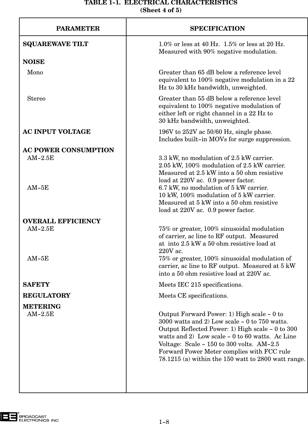
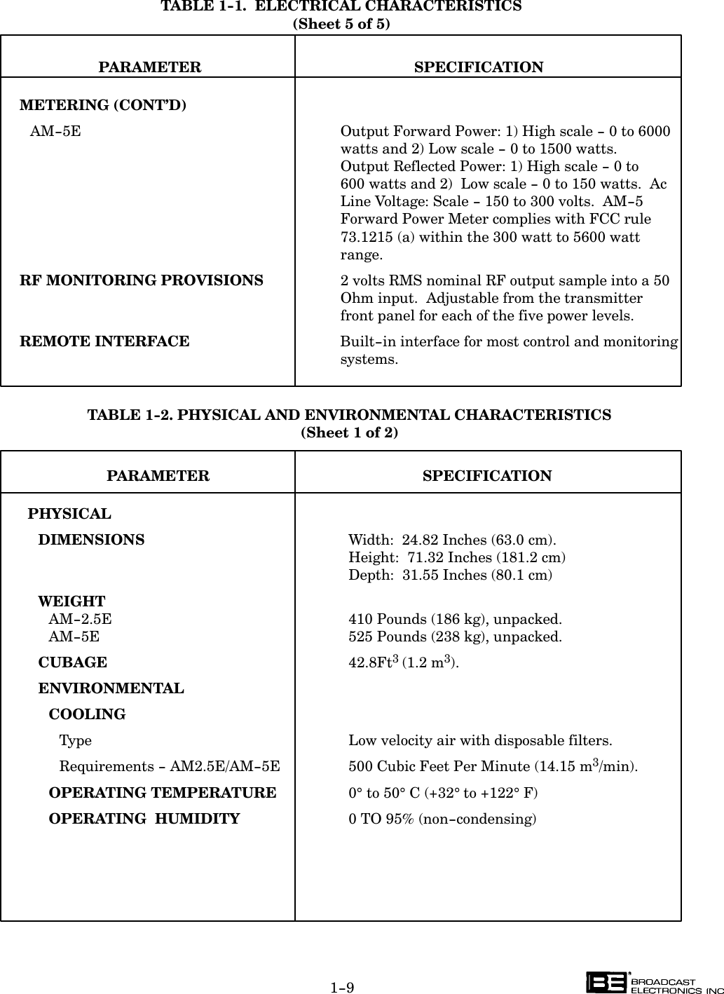
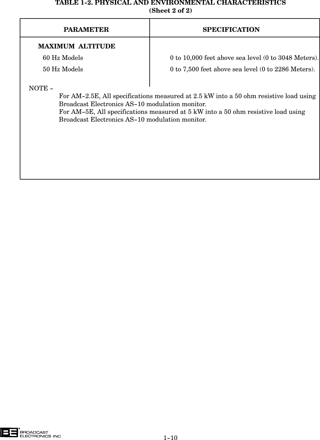
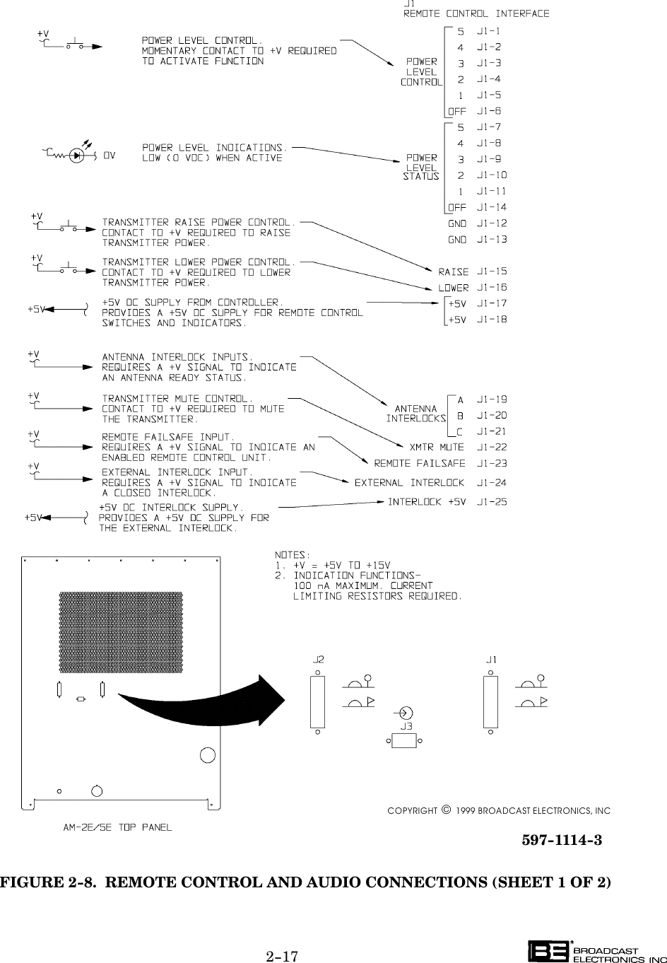
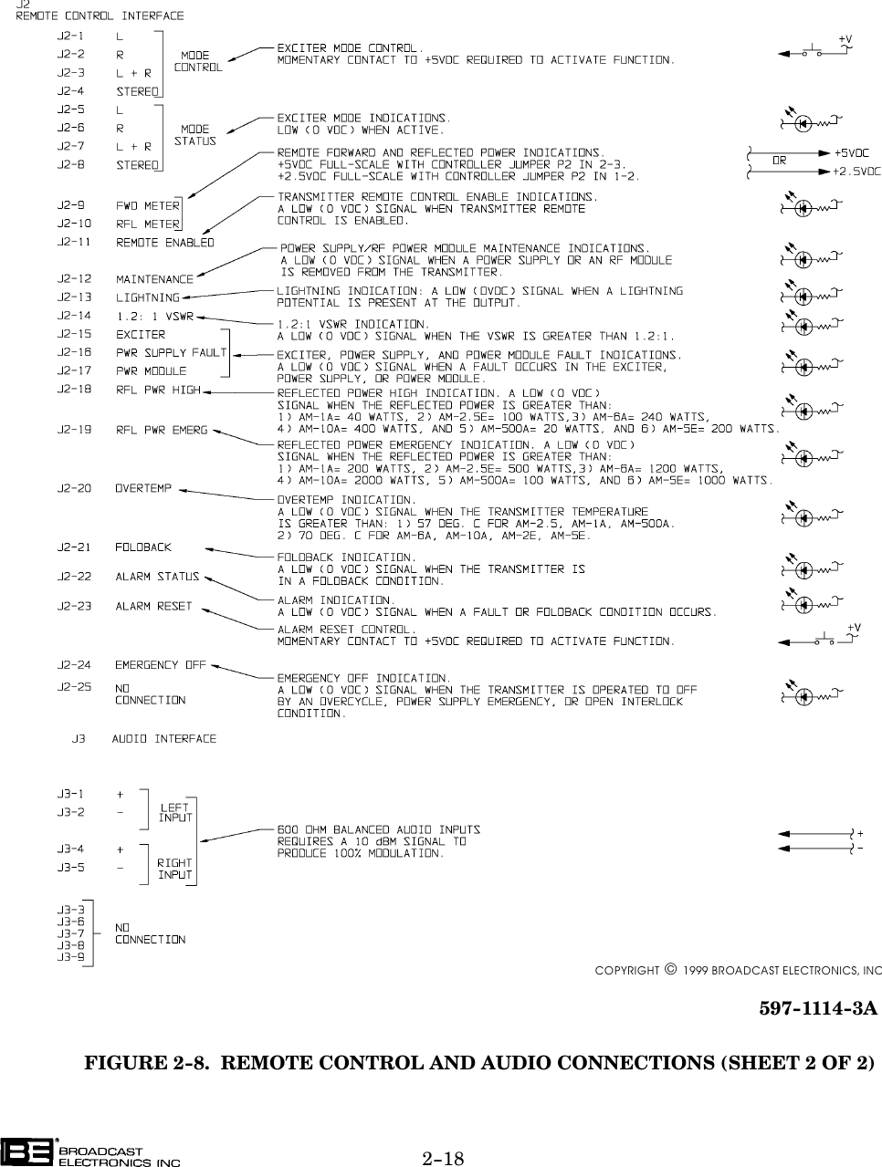
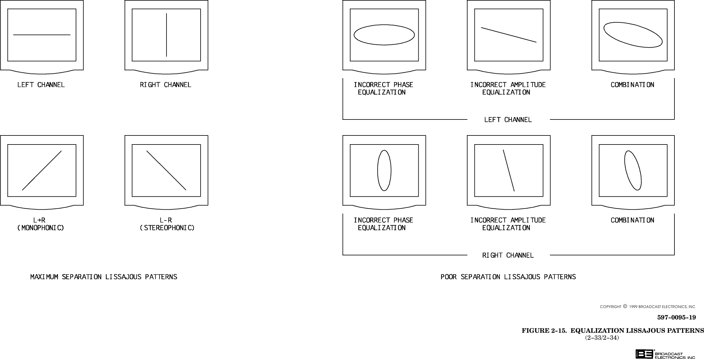
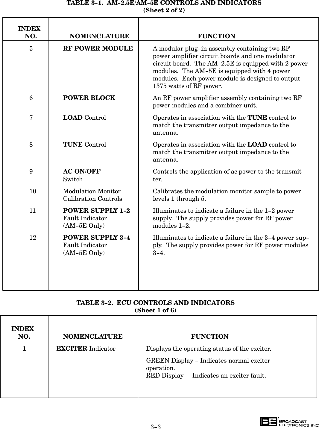
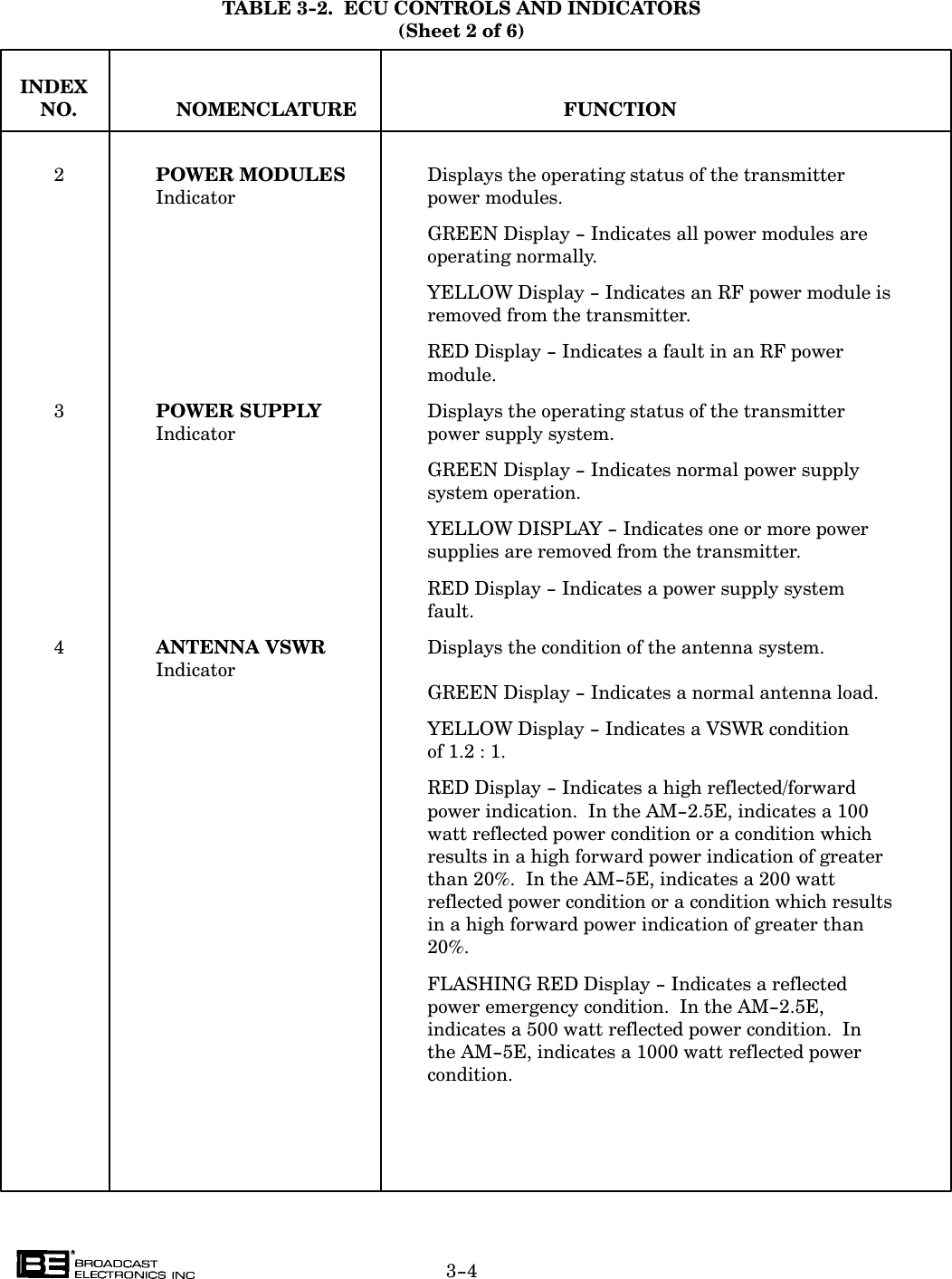
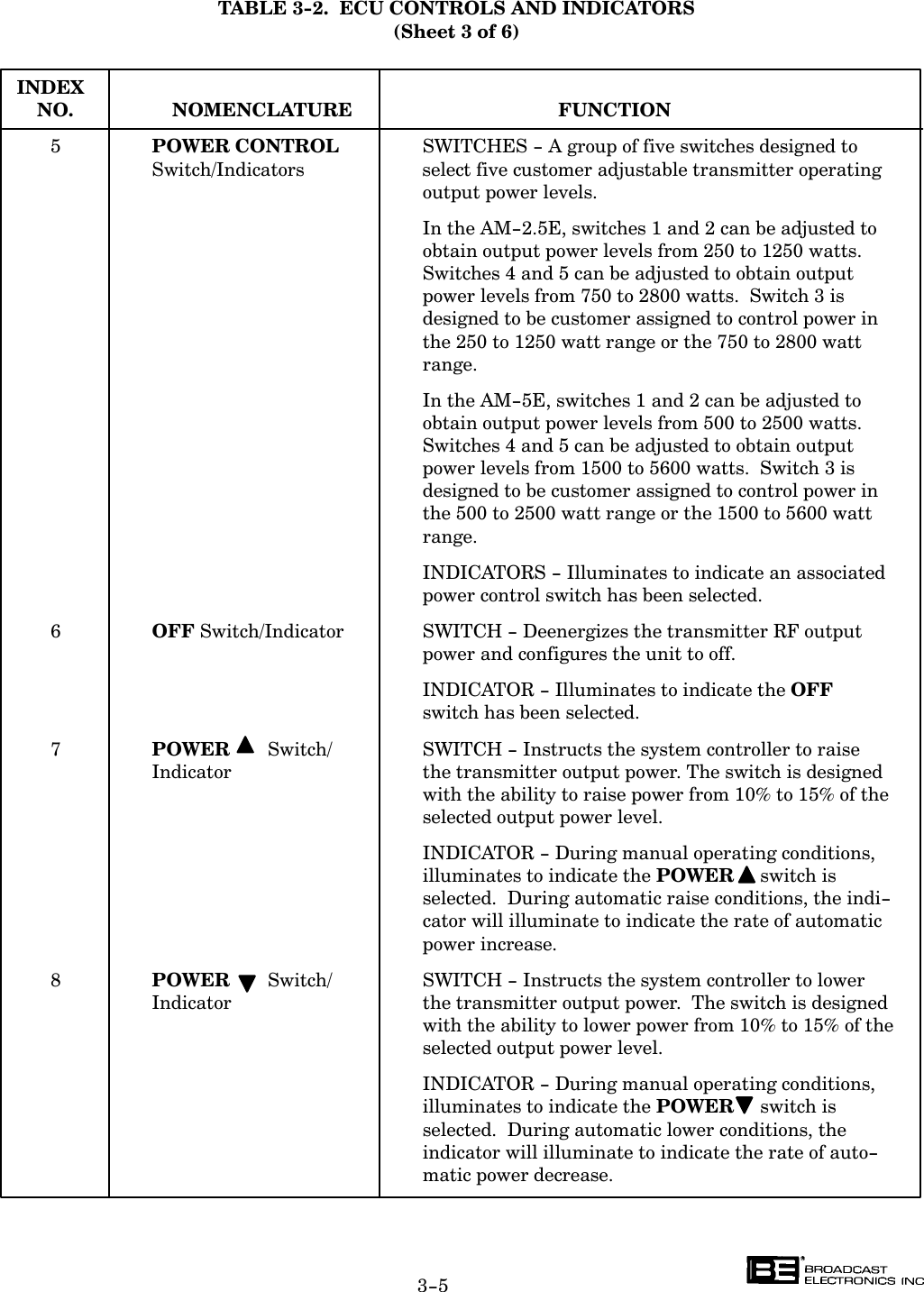
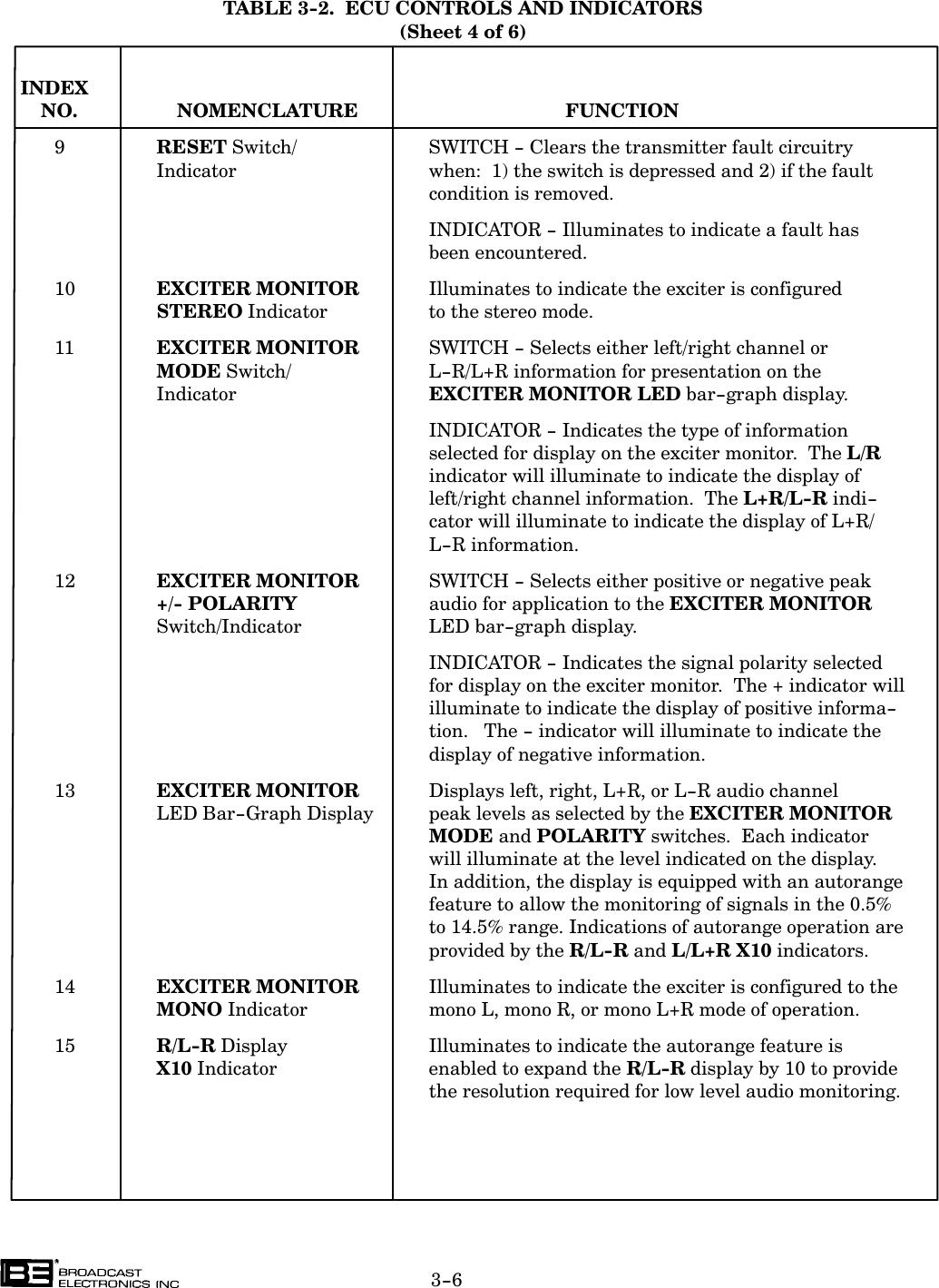
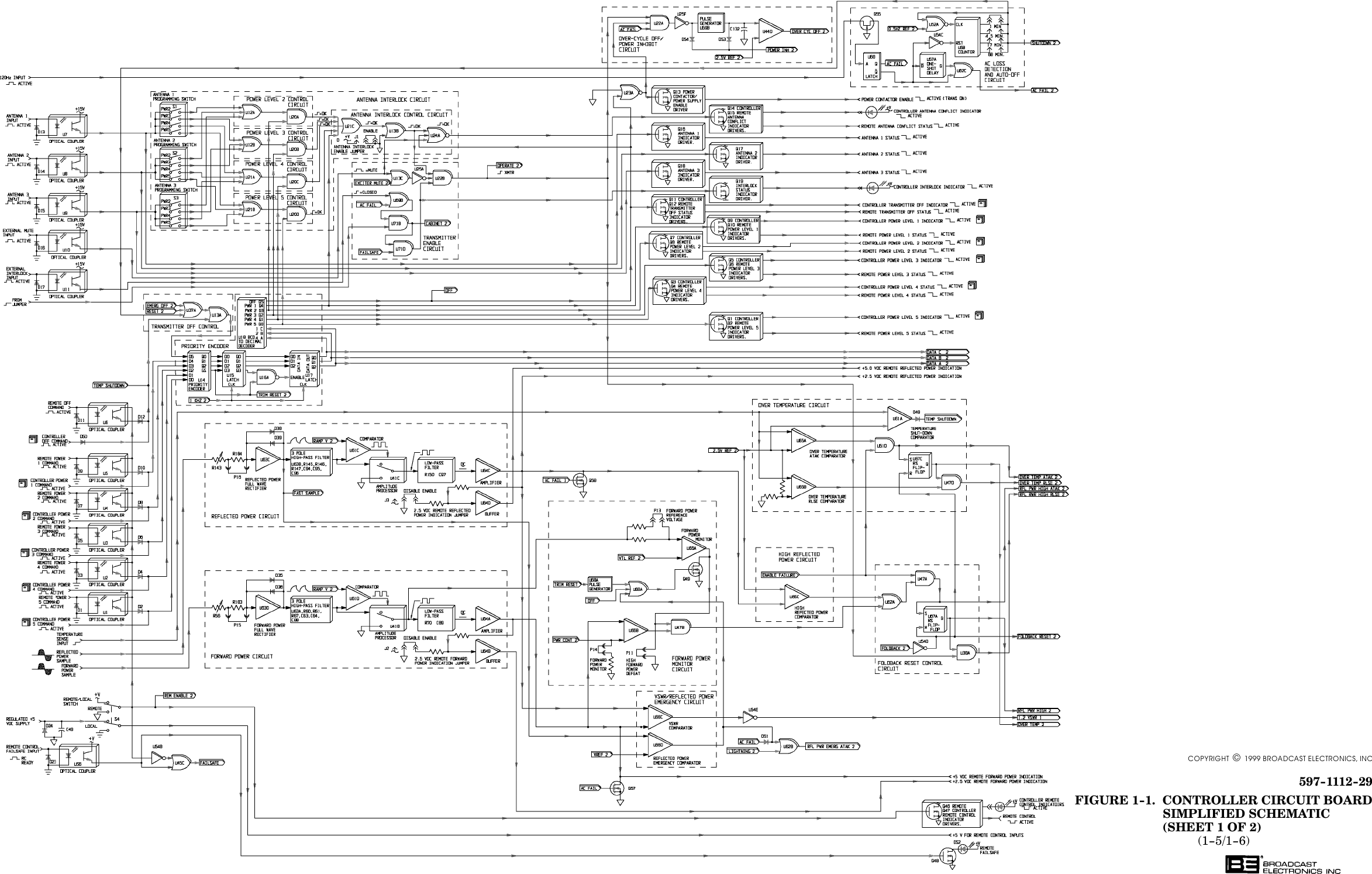
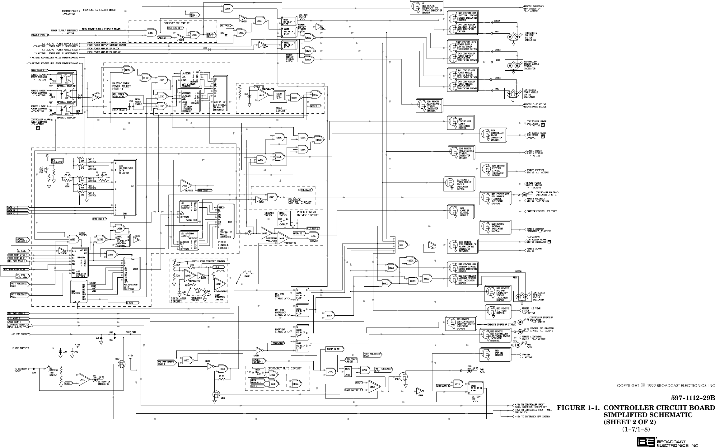
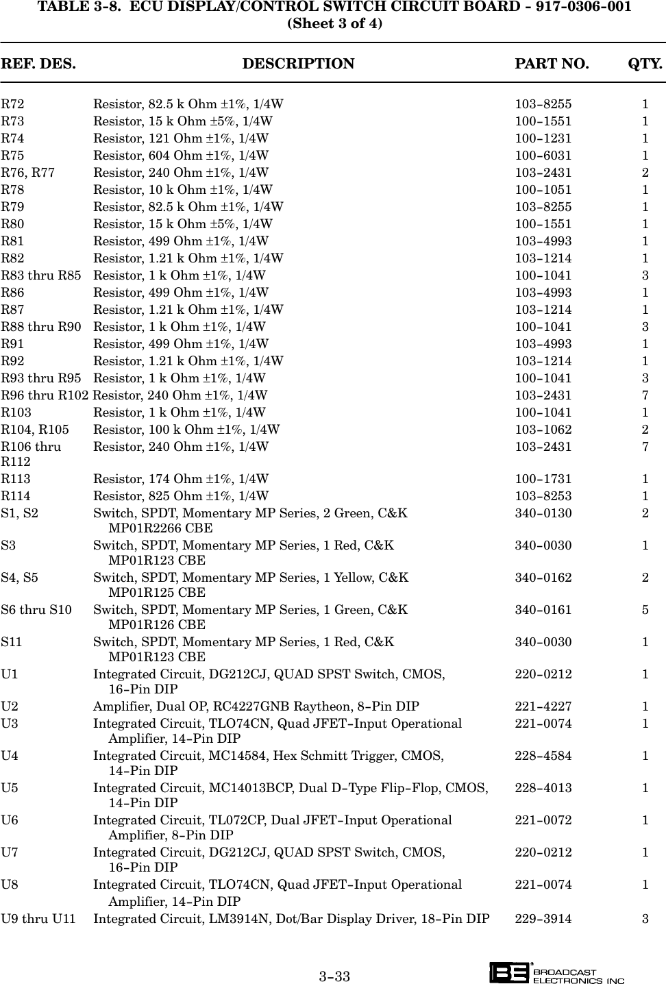
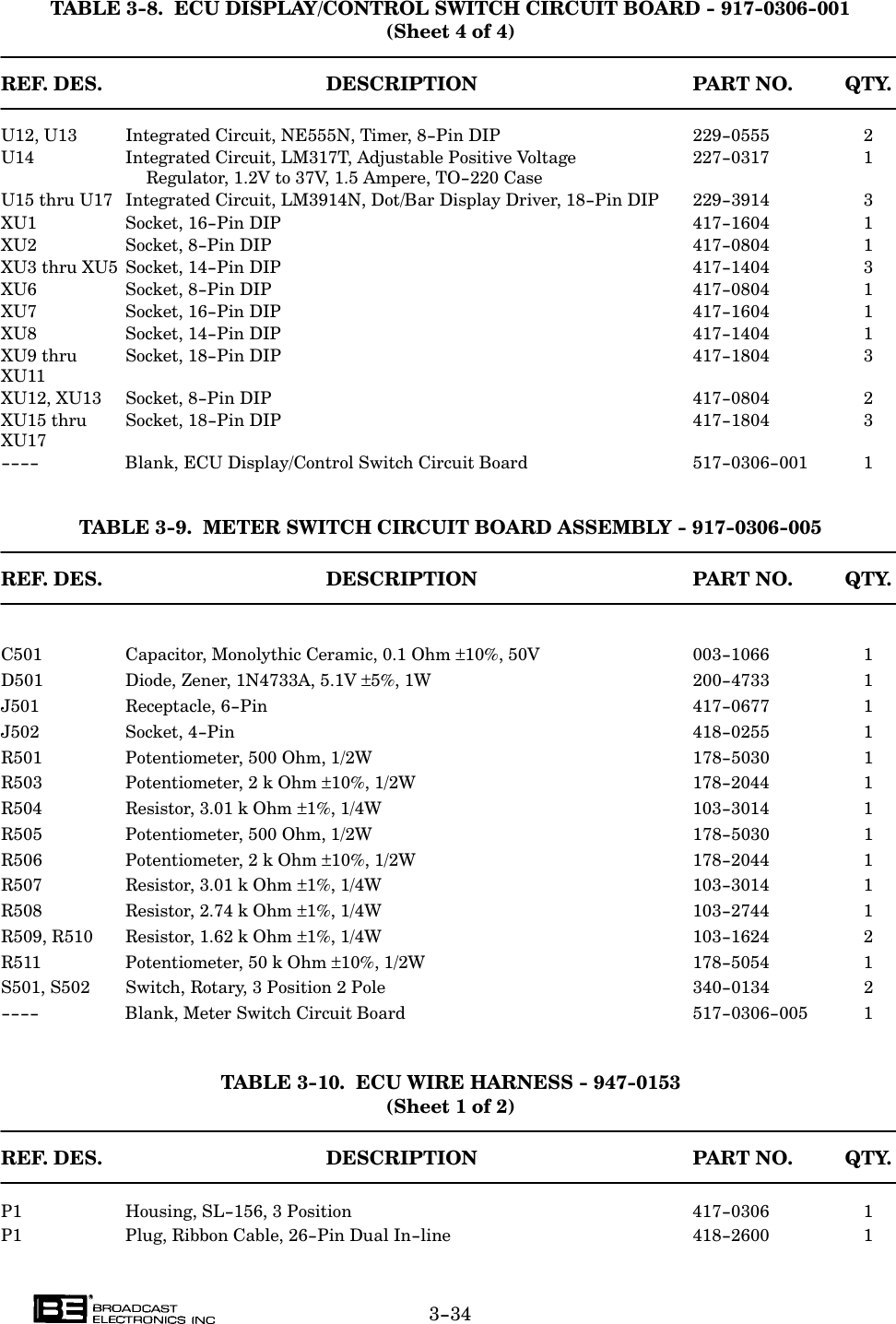
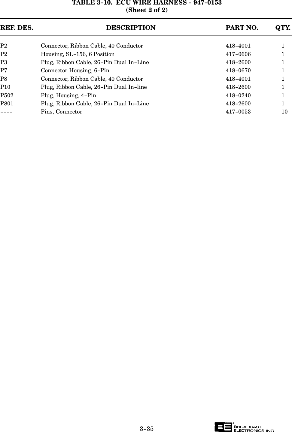
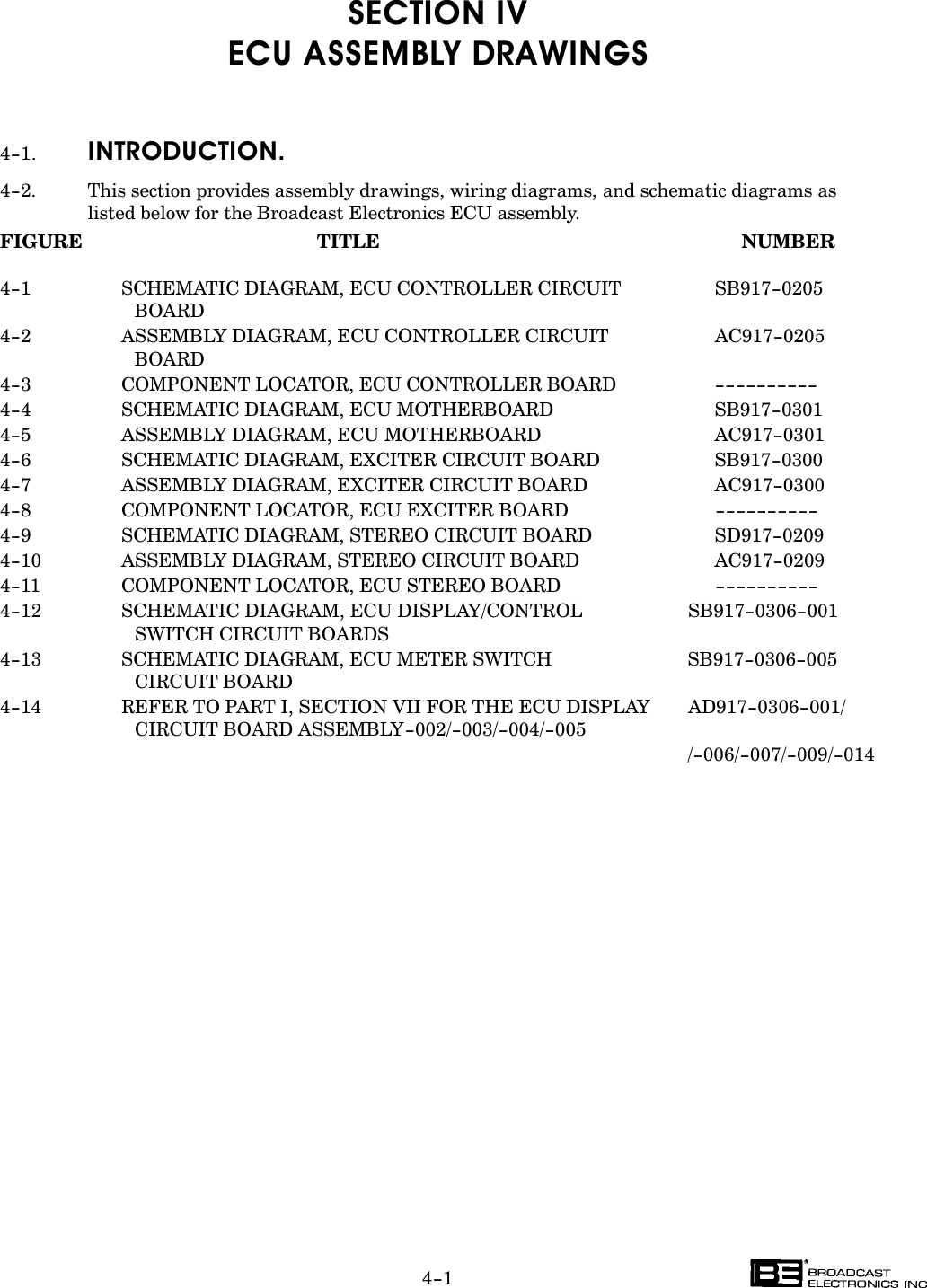
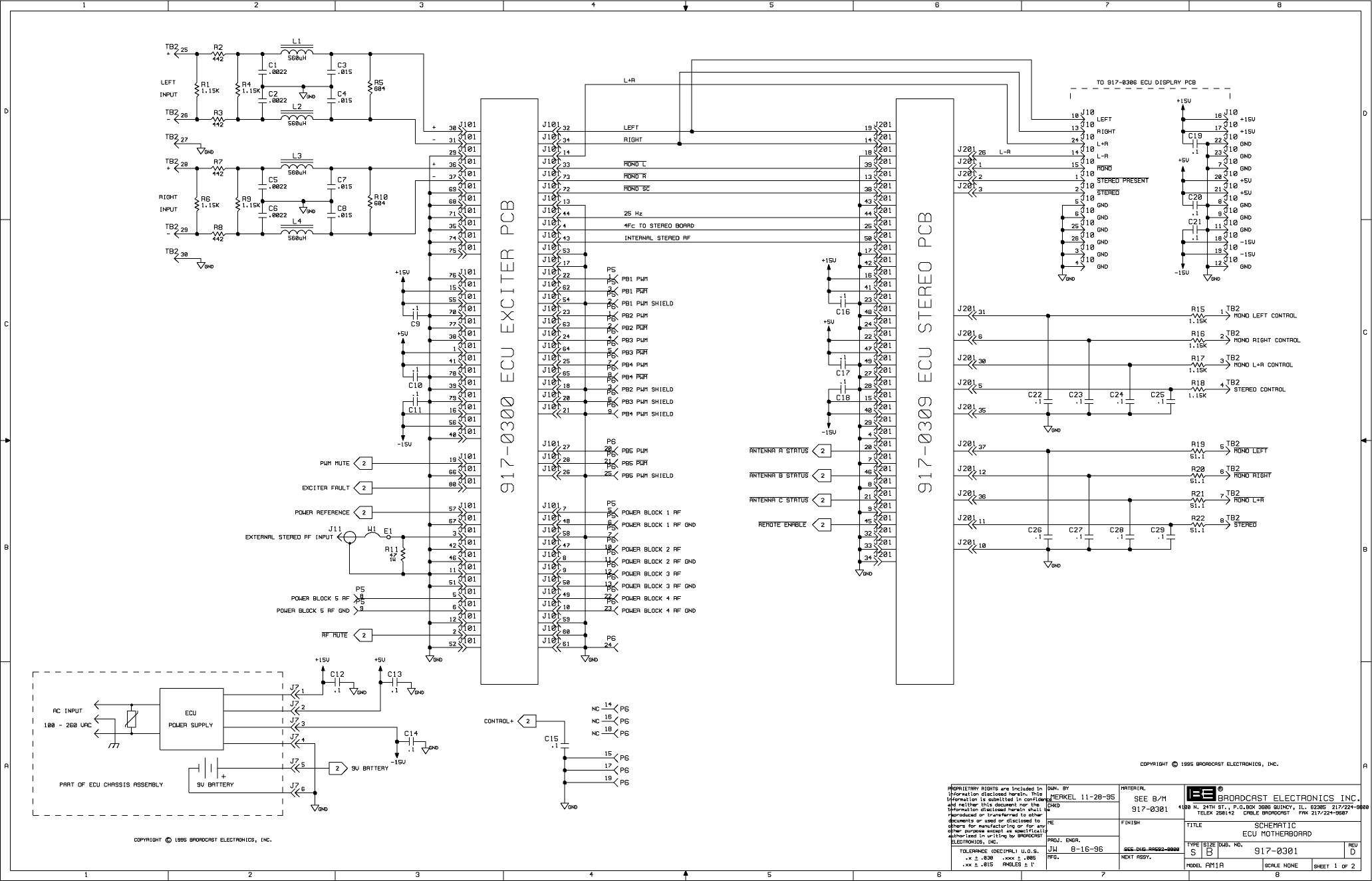
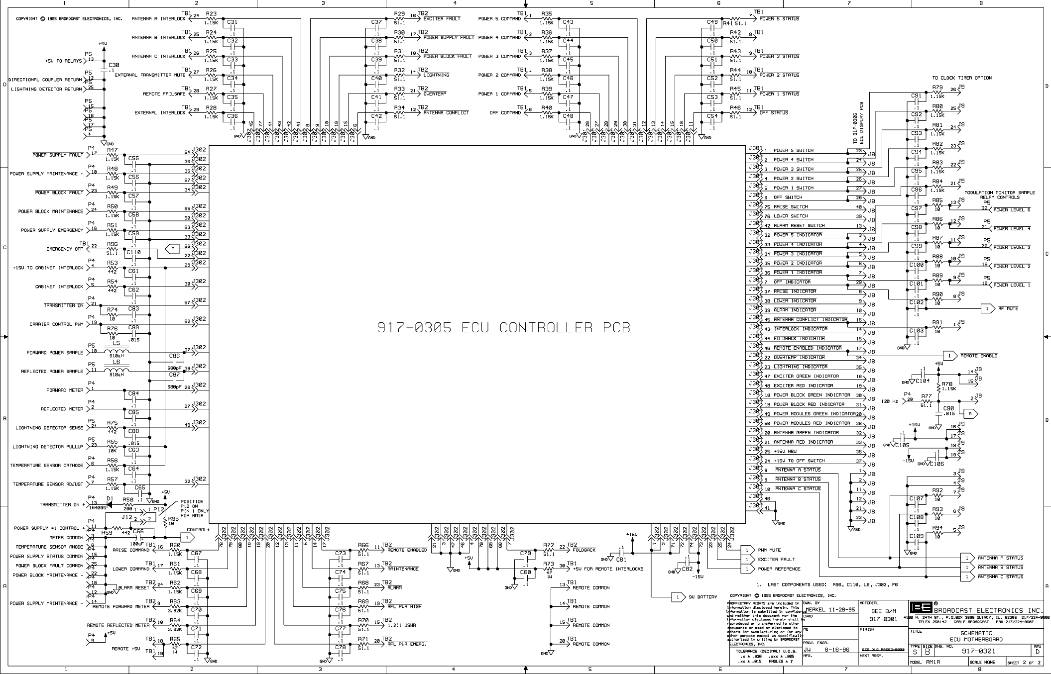
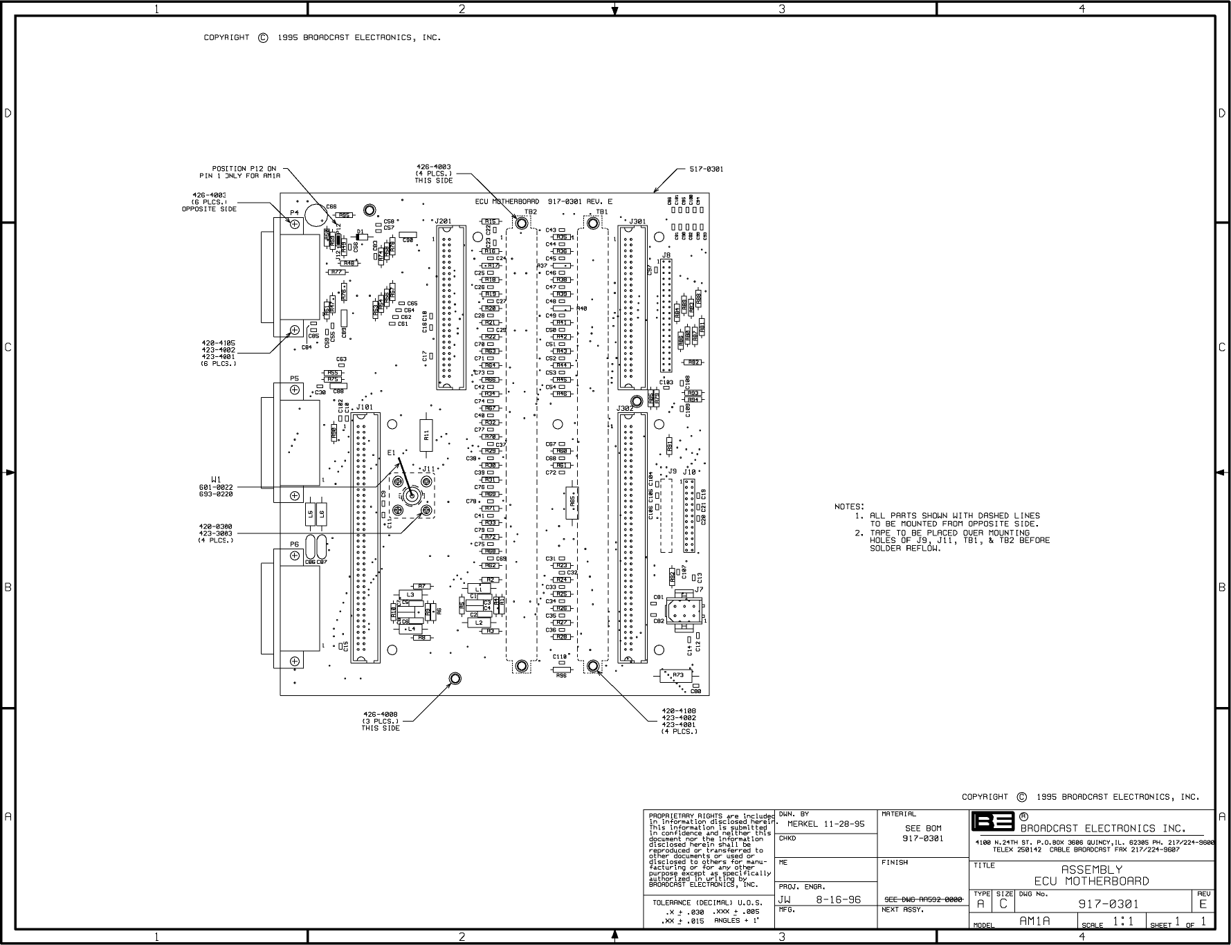
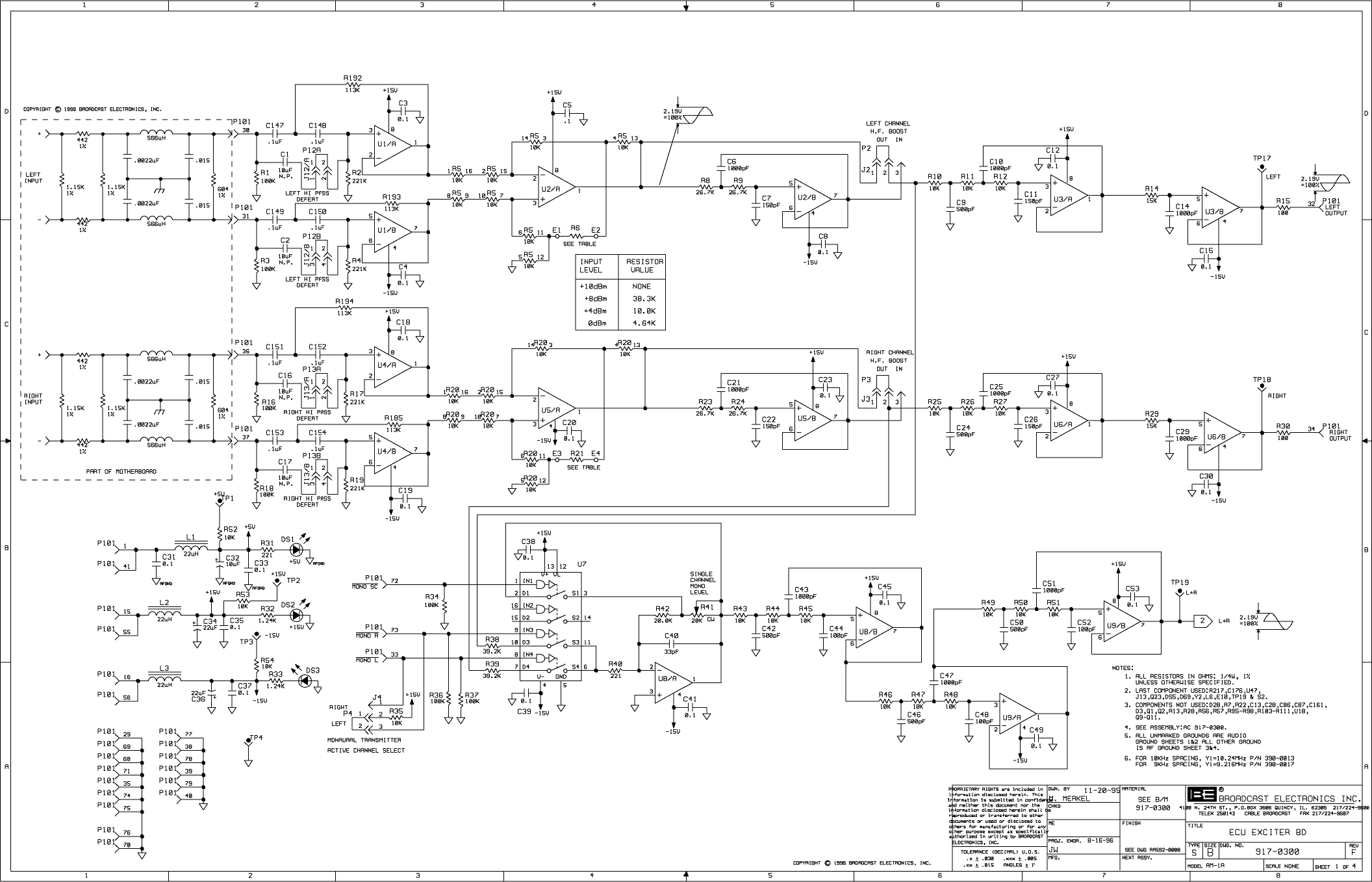
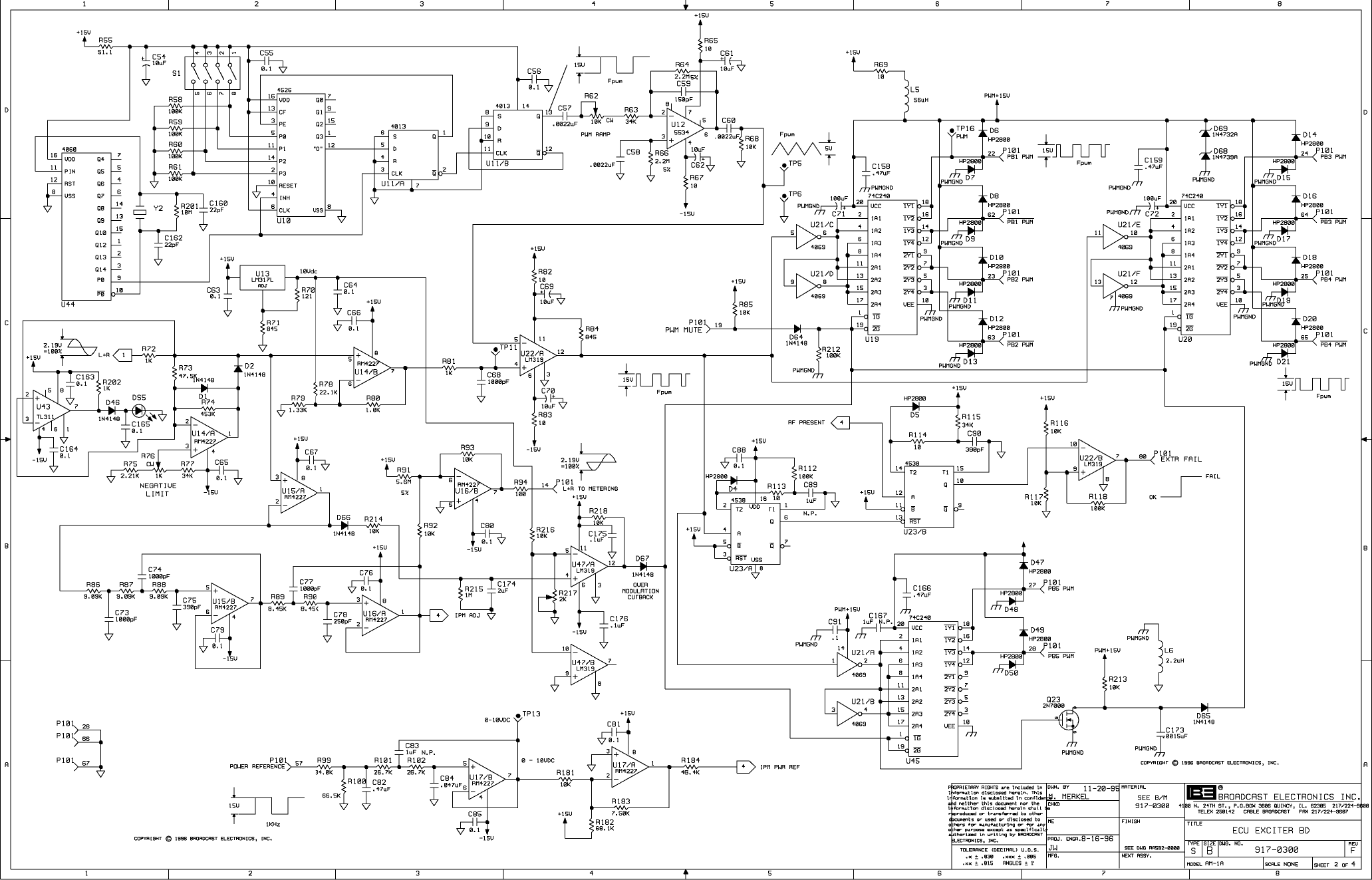
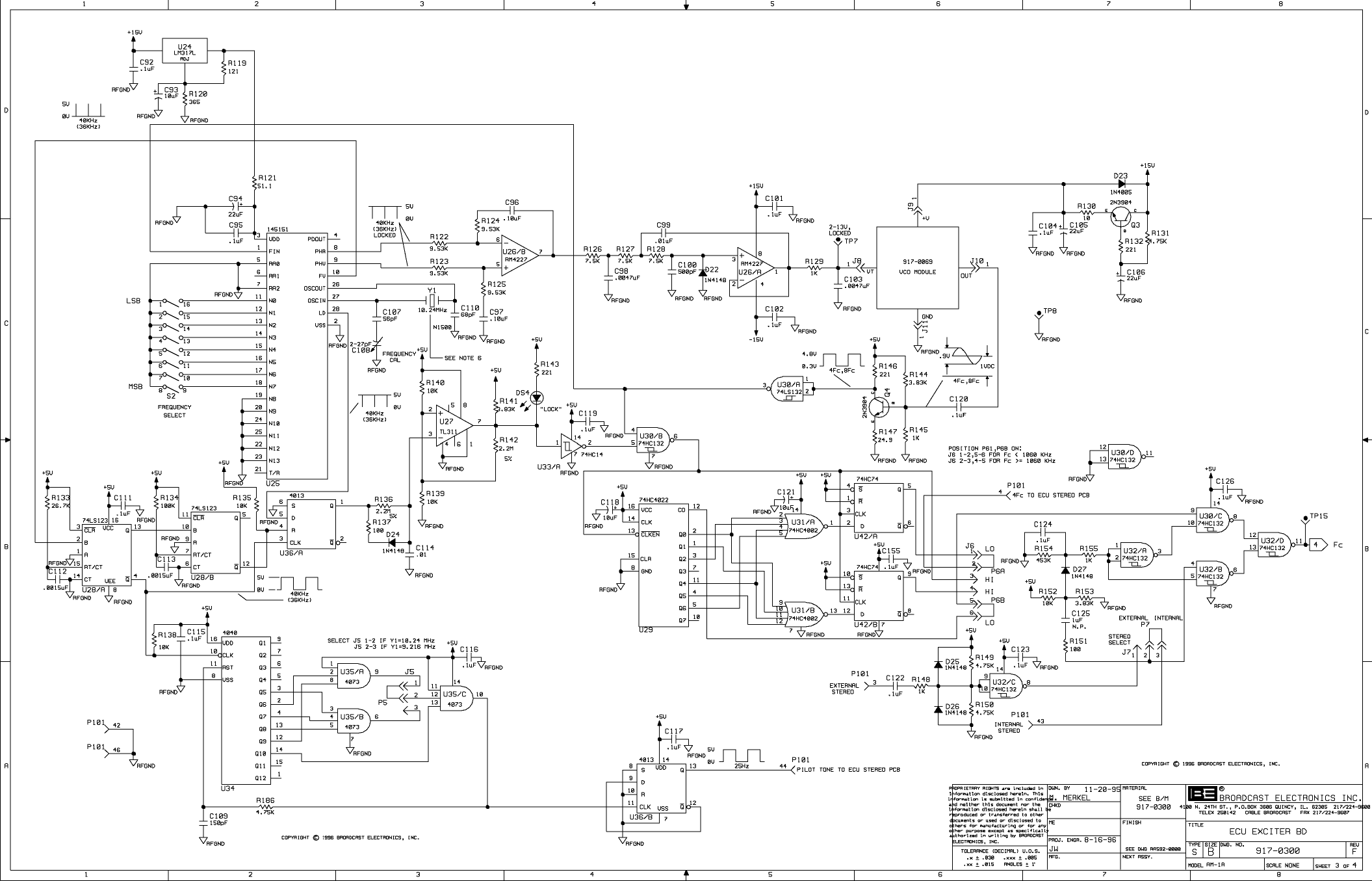
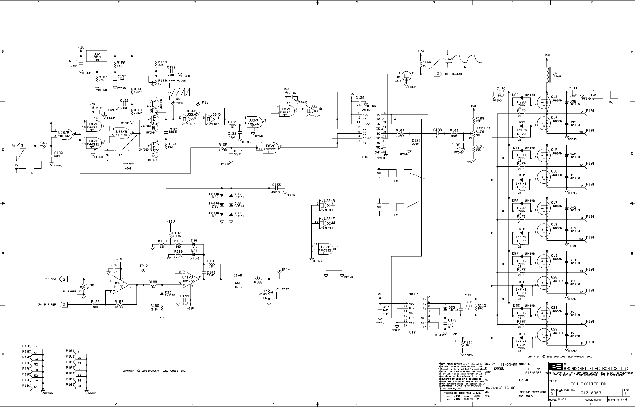
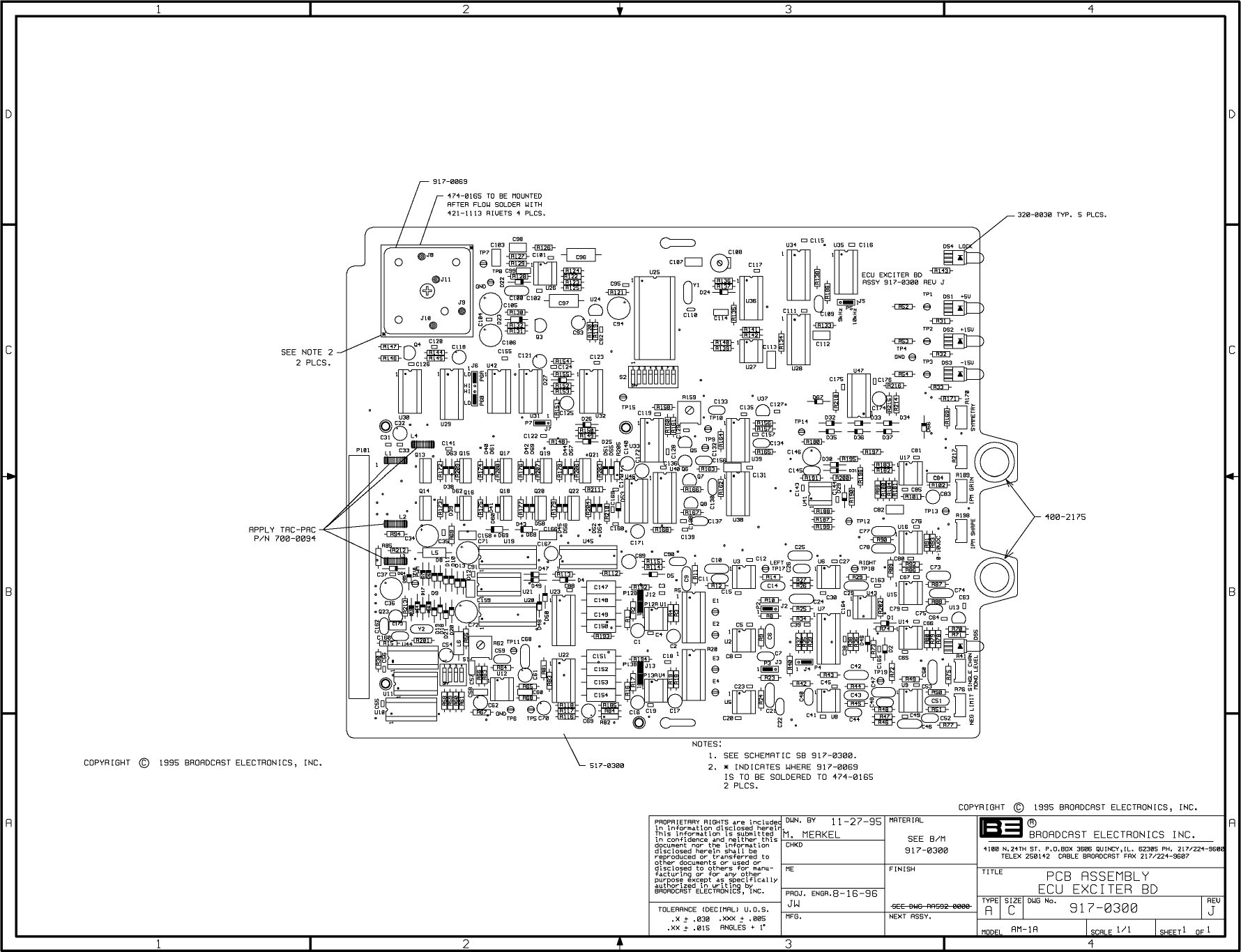
BEI Electronics 7EPTX-AM2-5E AM-2.5E, 2.5 KW AM Stereo Transmitter User Manual WARNINGS

BEI Electronics, LLC AM-2.5E, 2.5 KW AM Stereo Transmitter WARNINGS

Users Manual

WARNINGOPERATING HAZARDSREAD THIS SHEET AND OBSERVE ALL SAFETY PRECAUTIONSALL PERSONS WHO WORK WITH OR ARE EXPOSED TO  POWER TRANSISTORS MUST TAKE PRECAUTIONSTO PROTECT THEMSELVES AGAINST POSSIBLE SERIOUS BODILY INJURY.  EXERCISE EXTREME CAREAROUND SUCH PRODUCTS.  UNINFORMED OR CARELESS OPERATION OF THESE DEVICES CAN RESULTIN POOR PERFORMANCE, DAMAGE TO THE DEVICE OR PROPERTY, SERIOUS BODILY INJURY, AND POSSI-BLY DEATH.DANGEROUS HAZARDS EXIST IN THE OPERATION OF POWER TRANSISTORSThe operation of power tubes and power transistors involves one or more of the following hazards, any one of which,in the absence of safe operating practices and precautions, could result in serious harm to personnel.A. HIGH VOLTAGE – Normal operating voltages can be deadly.  Additional information follows.B. RF RADIATION – Exposure to RF radiation may cause serious bodily injury possibly resulting in blindness or death.  Cardiac pacemakers may be affected.  Additional information follows.C. BERYLLIUM – OXIDE POISONING – Dust or fumes from BeO ceramics used as thermal links with power transistors are highly toxic and can cause serious injury or death.  Additional information follows.D. HOT SURFACES – Surfaces of air–cooled heat sinks radiators can reach temperatures of 100 degrees centigrade and cause burns if touched.  Additional information follows.E. RF BURNS – Circuit boards with RF power transistors contain high RF potentials.  Do not operate an RF power module with the cover removed.HIGH VOLTAGEThe transmitter operates at voltages high enough to kill through electrocution.  Personnel should always break theprimary circuits when access to the transmitter is required.RADIO FREQUENCY RADIATIONExposure of personnel to RF radiation should be minimized, personnel should not be permitted in the vicinity of openenergized RF generating circuits, or RF transmission systems (waveguides, cables, connectors, etc.), or energizedantennas.  It is generally accepted that exposure to “high levels” of radiation can result in severe bodily injury includ-ing blindness.  Cardiac pacemakers may be affected.The effect of prolonged exposure to “low level” RF radiation continues to be a subject of investigation and controver-sy.  It is generally agreed that prolonged exposure of personnel to RF radiation should be limited to an absolute mini-mum.  It is also generally agreed that exposure should be reduced in working areas where personnel heat load isabove normal.  A 10 mW/cm2 per one tenth hour average level has been adopted by several U.S. Government agen-cies including the Occupational Safety and Health Administration (OSHA) as the standard protection guide for em-ployee work environments.  An even stricter standard is recommended by the American National Standards Institutewhich recommends a 1.0 mW/cm2 per one tenth hour average level exposure between 30 Hz and 300 MHz as thestandard employee protection guide (ANSI C95.1–1982).RF energy must be contained properly by shielding and transmission lines.  All input and output RF connections, suchas cables, flanges and gaskets must be RF leakproof.  Never operate a power tube without a properly matched RFenergy absorbing load attached.  Never look into or expose any part of the body to an antenna, open RF generatingcircuit, or RF transmission system while energized.  Monitor the tube and RF system for RF radiation leakage at regu-lar intervals and after servicing.  DANGER –– BERYLLIUM OXIDE CERAMICS (BeO) – AVOID BREATHING DUST OR FUMESBeO ceramic material is used as a thermal link to carry heat from a transistor to the heat sink.  Do not perform anyoperation on any BeO ceramic which might produce dust or fumes, such as grinding, grit blasting, or acid cleaning.Beryllium oxide dust or fumes are highly toxic and breathing them can result in serious personal injury or death.  BeOceramics must be disposed of only in a manner prescribed  by the device manufacturer.HOT SURFACESHeat sinks and reject loads are air–cooled or conduction–cooled.  The air–cooled external surface can operate at ahigh temperature (up to 100°C).  All hot surfaces may remain hot for an extended time after the transmitter is oper-ated to off.  To prevent serious burns, take care to prevent and avoid any bodily contact with these surfaces both dur-ing and for a reasonable cooling down period after operation.
TRANSMITTER WARRANTY VOID NOTICETHE PRODUCT WARRANTY WILL BE VOID IF THE TRANSMITTER IS INSTALLED AT A SITE WITHINADEQUATE LIGHTNING PROTECTION AND A DEFECTIVE TRANSMISSION LINE SYSTEM.The transmitter is covered by a two year limited product warranty from Broadcast ElecĆtronics.  However, the transmitter must be properly installed at a site with adequatelightning protection and transmission line systems.  TO ENSURE THE TRANSMITĆTER WARRANTY IS VALID, the transmitter must be installed: 1) as described by theINSTALLATION procedures presented in SECTION II of this manual, 2) at a transmittersite with a lightning protection system described in TRANSMITTER SITE LIGHTNINGPROTECTION SYSTEM CHECKOUT (refer to  SECTION II of this manual), and 3) at atransmitter site with a transmission line system described in TRANSMISSION LINEAND ANTENNA CHECKOUT (refer to SECTION II of this manual).  FAILURE TOPROPERLY INSTALL THE TRANSMITTER, PROVIDE AN ADEQUATE LIGHTĆNING PROTECTION SYSTEM, OR PROVIDE AN ADEQUATE TRANSMISSIONLINE SYSTEM WILL VOID THE WARRANTY ON THE TRANSMITTER.   If anyquestions develop concerning the transmitter warranty and installation site systems, conĆtact the Broadcast Electronics Customer Service Department.BROADCAST ELECTRONICS, INC.
NOTICE TO THE EQUIPMENT USERFCC Rule 73.1590 mandates the licensee of each AM station to make measurements forspurious and harmonic emissions to show compliance with the transmission system reĆquirements of Section 73.44 of the Commission's Rules.  It is the broadcast station's responĆsibility to ensure that the audio signal applied to a Broadcast Electronics E-Series AMtransmitter conforms to the audio standard NRSC-1 (published as ANSI/EIA-549-1988).This is a mandatory requirement to ensure that the equipment complies to Section 73.44and Section 73.128(C) of the Commission's Rules.BROADCAST ELECTRONICS, INC.
WARNING WARNINGOPERATING HAZARDSWARNINGWARNINGTHE TRANSMITTER CONTAINS MULTIPLE CIRCUITGROUNDS WITH HIGH AC AND DC POTENTIALS WITHRESPECT TO THE CABINET WHICH IS AT EARTH POĆTENTIAL.  DO NOT ENERGIZE THE TRANSMITTERWITH TEST EQUIPMENT CONNECTED TO THETRANSMITTER OUTPUT NETWORK, RF POWER MODĆULE, RF COMBINER, OR POWER SUPPLY COMPOĆNENTS.The Broadcast Electronics AM transmitters contain high voltages and currents.  If safety precautions arenot practiced, contact with the high voltages and currents could cause serious injury or death.  The transĆmitter is equipped with many built-in safety features, however good judgement, care, and common sensemust be practiced to prevent accidents.  In addition to high voltages and currents, the AM transmitters contain multiple circuit grounds withhigh ac and dc potentials with respect to the cabinet which is at earth potential.  The potentials couldcause serious injury or death if maintenance personnel simultaneously touch a circuit ground and thecabinet.  As a result, operation of the transmitter with test equipment connected to transmitter outputnetwork, RF power module, RF combiner, or power supply components is extremely dangerous and mustnot be attempted.  Therefore, never energize the transmitter with test equipment connected to the transĆmitter output network, RF power module, RF combiner, or power supply components.  Test equipmentmay be connected to the ECU circuit boards from the front of the transmitter using the supplied extendercircuit board with power energized if required.
 Broadcast Electronics 1999   ALL RIGHTS RESERVED         Printed in the U.S.A.-i -SCOPE OF MANUALThis manual consists of two sections which provides the following information for the BroadcastElectronics AM-2.5E and AM-5E AM Broadcast Transmitters.A. PART I - Contains information relative to installation, operation, and maintenance applicable to the overall transmitter.B. PART II - Contains detailed information for the following transmitter modular  units.1. POWER SUPPLY ASSEMBLY2. RF POWER MODULE3. OUTPUT NETWORK4. EXCITER/CONTROLLER UNIT (ECU)PART I  -  TABLE OF CONTENTSPARAGRAPH PAGE NO.SECTION I GENERAL INFORMATION1-1 INTRODUCTION 1-11-3 EQUIPMENT DESCRIPTION 1-11-4 GENERAL 1-11-6 EXCITER/CONTROL UNIT 1-11-12 OUTPUT NETWORK ASSEMBLY 1-41-13 RF POWER MODULE 1-41-15 POWER SUPPLY 1-41-16 COMBINER ASSEMBLY 1-41-17 TRANSMITTER CONFIGURATIONS 1-51-19 ACCESSORIES AND SPARE PARTS KITS 1-51-21 EQUIPMENT SPECIFICATIONS 1-5SECTION II INSTALLATION2-1 INTRODUCTION 2-12-3 UNPACKING 2-12-6 ENVIRONMENTAL REQUIREMENTS 2-12-8 COOLING AIR REQUIREMENTS 2-12-12 PRIMARY POWER 2-12-14 INSTALLATION 2-12-16 EQUIPMENT PLACEMENT 2-22-19 COMPONENT INSTALLATION 2-22-22 ECU CIRCUIT BOARDS 2-22-23 RF POWER MODULES 2-22-24 POWER SUPPLY 2-72-25 BATTERY INSTALLATION 2-82-26 CIRCUIT BOARD PROGRAMMING 2-82-28 EXCITER CIRCUIT BOARD 2-82-37 STEREO CIRCUIT BOARD 2-122-42 CONTROLLER CIRCUIT BOARD 2-12
-ii -PARAGRAPH PAGE NO.2-55 POWER SUPPLY CIRCUIT BOARD 2-152-58 REMOTE CONTROL 2-162-59 GENERAL 2-162-84 WIRING 2-202-86 AUDIO INPUT CONNECTION 2-202-88 EXTERNAL STEREO RF INPUT 2-202-89 AM-2.5E/AM-5E RF TRANSMISSION  2-20LINE CONNECTION2-90 EXTERNAL INTERLOCK 2-202-91 MODULATION MONITOR 2-202-92 AC POWER CONNECTIONS 2-222-95 GROUND 2-222-96 TRANSMITTER SITE LIGHTNING PROTECTION 2-22SYSTEM CHECKOUT2-98 ANTENNA BALL-GAP LIGHTNING ARRESTOR 2-252-102 ANTENNA-TUNING-UNIT SPARK-GAP  2-25LIGHTNING ARRESTOR2-103 TRANSMITTER SITE GROUNDING SYSTEM 2-252-104 CABLE PROTECTION 2-262-110 ANTENNA RF FEED LINE 2-262-111 TRANSMISSION LINE AND ANTENNA CHECKOUT 2-262-113 ANTENNA VSWR 2-262-114 COAXIAL SWITCH CONTROLLER 2-262-115 ATU AND PHASOR CHECKOUT 2-282-116 INITIAL CHECKOUT 2-282-118 PRELIMINARY OPERATION AND ADJUSTMENT 2-282-120 TUNING 2-282-126 POWER LEVEL AND MODULATION MONITOR  2-29CALIBRATION ADJUSTMENTS2-138 STEREO ADJUSTMENT 2-302-149 SINGLE CHANNEL LEVEL 2-32SECTION III OPERATION3-1 INTRODUCTION 3-13-3 CONTROLS AND INDICATORS 3-13-5 OPERATION 3-123-6 TURN-ON 3-123-14 TURN OFF 3-133-16 METERING 3-133-17 FORWARD POWER 3-133-18 REFLECTED POWER 3-133-19 POWER ADJUST 3-133-21 MONO/STEREO OPERATION 3-143-23 STEREO OPERATION 3-143-24 MONO OPERATION 3-143-27 PILOT CONTROL 3-143-29 EXCITER MONITOR OPERATION 3-143-31 MONO/STEREO INDICATIONS 3-143-32 INPUT SELECTION 3-143-33 POLARITY SELECTION 3-153-34 X10 AUTORANGE INDICATIONS 3-15
-iii-PARAGRAPH PAGE NO.3-35 FAULT RESET 3-153-37 POWER SUPPLY FAULT RESET 3-153-39 OVER-CYCLE OFF 3-153-41 OVER-MODULATION PWM MUTE 3-153-43 TRANSMITTER MONITOR 3-153-45 BATTERY TEST 3-153-47 CONTROLLER PWM MUTE INDICATOR 3-163-49 CONTROLLER REMOTE FAIL-SAFE INDICATOR 3-163-51 EXCITER LOCK INDICATOR 3-163-53 EXCITER +5V/+15V/-15V INDICATORS 3-163-55 STEREO EQUALIZATION INDICATORS 3-163-57 RF POWER MODULE INDICATORS 3-163-59 POWER SUPPLY INDICATORS 3-163-61 EXCITER NEGATIVE LIMITER INDICATOR 3-163-63 HIGH/LOW AC LINE CONDITIONS 3-16SECTION IV THEORY OF OPERATION4-1 INTRODUCTION 4-14-5 FUNCTIONAL DESCRIPTION 4-14-6 ECU 4-14-7 GENERAL 4-14-8 STEREO CIRCUIT BOARD 4-14-11 EXCITER CIRCUIT BOARD 4-14-13 CONTROLLER CIRCUIT BOARD 4-24-18 POWER SUPPLY 4-24-19 RF POWER MODULE 4-24-24 RF COMBINER 4-74-27 OUTPUT NETWORK 4-74-31 POWER SUPPLY 4-84-34   POWER SUPPLY CIRCUIT BOARD 4-84-39 METERING 4-94-42 COOLING FANS 4-94-44 INTERFACE CIRCUIT BOARD (AM-5E ONLY) 4-94-46 DETAILED DESCRIPTION 4-94-47 POWER SUPPLIES 4-94-49 AC INPUT CIRCUITRY 4-94-53 ECU POWER SUPPLY ASSEMBLY 4-104-57 TRANSMITTER FLUSHING FANS 4-104-60 LOW-VOLTAGE POWER SUPPLY TRANSFORMER 4-104-62 POWER SUPPLY CIRCUIT BOARD 4-104-65 CONVENTIONAL RECTIFIER CIRCUITRY 4-134-68 SWITCHING POWER SUPPLY CIRCUIT 4-134-76 MODULATOR CIRCUIT BOARD 4-144-81 POWER AMPLIFIER CIRCUIT BOARDS 4-154-86 SEQUENCE OF OPERATION 4-154-91 RF CIRCUITRY 4-164-92 EXCITER CIRCUIT BOARD 4-164-98 STEREO CIRCUIT BOARD 4-174-102 RF POWER MODULE 4-174-109 RF COMBINER 4-214-110 HARMONIC BAND-PASS FILTER 4-22
-iv-PARAGRAPH PAGE NO.4-111 DIRECTIONAL COUPLER CIRCUIT BOARD 4-224-115 T-MATCHING NETWORK 4-224-116 LIGHTNING PROTECTION CIRCUIT BOARD 4-224-117 LIGHTNING DETECTION CIRCUIT BOARD 4-234-119 RF OUTPUT POWER CONTROL CIRCUITRY 4-23SECTION V MAINTENANCE5-1 INTRODUCTION 5-15-3 SAFETY CONSIDERATIONS 5-15-6 FIRST LEVEL MAINTENANCE 5-15-8 ROUTINE MAINTENANCE 5-15-9 INSPECTION AND CLEANING 5-25-10 CONTROLLER BATTERY 5-25-11 AIR FILTERS 5-25-12 FLUSHING FANS 5-25-14 SPARK GAP 5-25-15 SECOND LEVEL MAINTENANCE 5-25-18 ELECTRICAL ADJUSTMENTS 5-45-20 TRANSMITTER FREQUENCY RE-PROGRAMMING 5-45-22 TROUBLESHOOTING 5-45-24 TRANSMITTER INDICATORS 5-55-25 RF POWER MODULE REMOVAL 5-85-26 TRANSMITTER TROUBLESHOOTING 5-8PROCEDURES5-27 TRANSMITTER COMPONENT LOCATIONS 5-85-28 COMPONENT REPLACEMENT PROCEDURE 5-135-34 INTEGRATED CIRCUITS 5-14SECTION VI PARTS LIST6-1 INTRODUCTION 6-1SECTION VII DRAWINGS7-1 INTRODUCTION 7-1LIST OF TABLESTABLE DESCRIPTION PAGE NO.1-1 ELECTRICAL CHARACTERISTICS 1-51-2 PHYSICAL AND ENVIRONMENTAL  1-9CHARACTERISTICS3-1 AM-2.5E/AM-5E CONTROLS AND INDICATORS 3-13-2 ECU CONTROLS AND INDICATORS 3-33-3 POWER MODULE CONTROLS AND INDICATORS 3-115-1 AM-2.5E/AM-5E INDICATORS 5-55-2 AM-2.5E/AM-5E TROUBLESHOOTING 5-96-1 AM-2.5E/AM-5E REPLACEABLE PARTS LIST INDEX 6-1
-v -LIST OF ILLUSTRATIONSFIGURE DESCRIPTION PAGE NO.1-1 AM-2.5E TRANSMITTER 1-21-2 AM-5E TRANSMITTER 1-32-1 AM-2.5E TRANSMITTER INSTALLATION 2-32-2 AM-5E TRANSMITTER INSTALLATION 2-52-3 TRANSMITTER MOVING 2-72-4 COMPONENT INSTALLATION 2-92-5 EXCITER CIRCUIT BOARD PROGRAMMING 2-112-6 STEREO CIRCUIT BOARD PROGRAMMING 2-132-7 CONTROLLER CIRCUIT BOARD PROGRAMMING 2-142-8 REMOTE CONTROL AND AUDIO CONNECTIONS 2-172-9 AM-2.5E/AM-5E RF OUTPUT CONNECTIONS 2-212-10 AM-2.5E PRIMARY AC WIRING 2-232-11 AM-5E PRIMARY AC WIRING 2-242-12 ANTENNA LIGHTNING PROTECTION SYSTEM 2-272-13 TEST EQUIPMENT CONNECTIONS, POWER LEVEL 2-30CALIBRATION2-14 TEST EQUIPMENT CONNECTIONS, SEPARATION 2-312-15 EQUALIZATION LISSAJOUS PATTERNS 2-333-1 AM-2.5E/AM-5E CONTROLS AND INDICATORS 3-23-2 ECU CONTROLS AND INDICATORS 3-73-3 POWER MODULE CONTROLS AND INDICATORS 3-114-1 AM-2.5E BLOCK DIAGRAM 4-34-2 AM-5E BLOCK DIAGRAM 4-54-3 AM-2.5E/AM-5E POWER SUPPLY SIMPLIFIED  4-11SCHEMATIC4-4 AM-2.5E/AM-5E RF CIRCUITRY SIMPLIFIED  4-18SCHEMATIC5-1 REMOVING THE AIR FILTER 5-35-2 AM-2.5E COMPONENT LOCATOR 5-155-3 AM-5E COMPONENT LOCATOR 5-185-4 AM-2.5E/AM-5E ECU/POWER BLOCK/OUTPUT  5-21NETWORK ASSEMBLY COMPONENT LOCATORPART II  -  TABLE OF CONTENTSI - POWER SUPPLY ASSEMBLYII - RF POWER MODULEIII - OUTPUT NETWORKIV - EXCITER/CONTROLLER UNIT (ECU)
1-1SECTION IGENERAL INFORMATION1-1. INTRODUCTION.1-2. Information presented by this section provides a general description of the BroadcastElectronics AM-2.5E and AM-5E transmitters and lists equipment specifications.1-3. EQUIPMENT DESCRIPTION.1-4. GENERAL.1-5. The Broadcast Electronics AM-2.5E transmitter is a CE compliant 2.5 kW solid-stateC-QUAM stereo AM transmitter designed for continuous operation in the 522 kHz to1705 kHz broadcast band (refer to Figure 1-1).  The Broadcast Electronics AM-5E transĆmitter is a CE compliant 5 kW solid-state C-QUAM stereo AM transmitter designed forcontinuous operation in the 522 kHz to 1705 kHz broadcast band (refer to Figure 1-2). TheAM-2.5E and AM-5E transmitters consists of modular components assembled in a singlecabinet.  The modular components include:  1) an exciter/control unit, 2) an output networkassembly, 3) power block assemblies containing two RF power modules and a star combinerassembly, 4) power supply panel assemblies, and 5) an AC distribution panel assembly.Specific AM-2.5E/AM-5E features include:1. Built-in C-QUAM AM stereo circuitry.2. High efficiency Class E solid-state RF power amplifier modules.3. A high efficiency switching power supply.4. Star combiner assembly.  Each star combiner allows the removal of RF power mod-ules without the use of dummy modules or bypass switches.5. A built-in output matching network.6. A CMOS digital controller with extensive VSWR detection and foldback circuitry which reduces carrier interruptions by weather conditions.7. CE compliant design.1-6. EXCITER/CONTROL UNIT.  The transmitter exciter/control unit (ECU) is a modular asĆsembly containing plug-in stereo, exciter, and controller circuit boards.  In addition to thecircuit boards, the ECU is equipped with forward and reflected power meters to providetransmitter output power status indications.1-7. Stereo Circuit Board.  The ECU stereo circuit board is a modular plug-in assembly conĆtaining C-QUAM AM stereo circuitry.  The C-QUAM stereo system is a mode of AMstereo transmission utilizing amplitude modulated monaural (L+R) information and indeĆpendently quadrature modulated stereo (L-R) information.  The results produce a stereotransmission system compatible with mono receivers.1-8. The stereo circuit board is designed with remote/local controlled mono left, mono right,mono L+R, and stereo modes of operation.  Two equalization circuits are provided to allowthe transmitter to be configured for operation into two different antennas.C-QUAMis a registered trademark of Motorola Inc.
1-2FIGURE 1-1.  AM-2.5E TRANSMITTER  597-1114-1COPYRIGHT  1999 BROADCAST ELECTRONICS, INC
1-3COPYRIGHT  1999 BROADCAST ELECTRONICS, INC597-1114-2FIGURE 1-2.  AM-5E TRANSMITTER
1-41-9. Exciter Circuit Board.  The ECU exciter circuit board is a modular plug-in exciter assemĆbly.  Instrumentation amplifiers provide balanced left and right channel transformerlessaudio inputs.  The exciter carrier frequency is established by a digital frequency synthesizĆer.  The synthesizer is a phase-locked-loop circuit which provides extremely accurate andreliable carrier frequency operation.  A PWM (pulse-width-modulation) circuit is used togenerate an RF drive signal for application to a modulator circuit board in an RF powermodule.  If a stereo circuit board failure is encountered or when the stereo circuit board isremoved from the ECU chassis, the exciter circuitry is designed to automatically configureto monophonic operation.1-10. Controller Circuit Board.  All transmitter control operations are directed by the ECU conĆtroller circuit board.  The controller circuit board consists of CMOS logic control and moniĆtoring circuitry.  The circuitry is designed to interface to all popular remote control systemssuch as the Broadcast Electronics VMC-16 remote control system.1-11. The transmitter power is controlled by a power control circuit.  The circuit allows thetransmitter to be operated at five power levels.  A power trim circuit allows the transmitteroutput power to be adjusted to a precise level.  An antenna interlock circuit is provided toprevent the transmitter from operating into an incorrect antenna.  A reflected power detecĆtion circuit operates in association with the power control circuit to foldback the transmitĆter power during high VSWR conditions.  In addition to the reflected power detector, alightning detector circuit is provided to mute the transmitter when high voltage is presentat the transmitter output during a lightning storm.1-12. OUTPUT NETWORK ASSEMBLY.  Matching of the transmitter impedance to the antenna isaccomplished by the output network assembly.  The assembly is equipped with an LC T network to match the transmitter output to the antenna.  A bandpass filter is proĆvided to attenuate all harmonic frequencies to FCC, DOC, and CCIR levels.  The assemblyalso contains the lightning detection circuit board, a lightning protection circuit board, anda directional coupler assembly.1-13. RF POWER MODULE.  The AM-2.5E and AM-5E transmitters are equipped with RF powĆer modules.  A power module is a modular plug-in assembly containing two RF power amĆplifier circuit boards and one modulator circuit board.  Each power module is equippedwith MOSFET transistors to produce approximately 1375 watts of RF power.1-14. The RF power modules are designed using Class E amplifier technology.  A Class E ampliĆfier exhibits high efficiency and provides superior audio performance.  In addition to thesuperior efficiency and audio performance, the power modules are designed to be removedfrom the chassis for maintenance.  The remaining power modules will provide full power tomaintain on-air operation.1-15. POWER SUPPLY.  A modular switching power supply provides operating potentials for twoRF power modules.  The power supply  design uses an SCR controlled bridge to rectify theac line voltage into a dc potential.  The supply is filtered and routed to the RF power modĆules for control and regulation.  A fault detection circuit monitors power supply activity forfailure conditions.  A separate modular switching power supply provides operating potenĆtials for the ECU circuitry.1-16. COMBINER ASSEMBLY.  The AM-2.5E and AM-5E are equipped with a star combiningsystem.  The system combines the outputs of the RF power modules to provide:  1) a 2.5kW output in AM-2.5E models and 2) a 5 kW output in AM-5E models.  If a power moduleis removed from the chassis, the remaining power modules will continue operation to mainĆtain on-air operation.
1-51-17. TRANSMITTER CONFIGURATIONS.1-18. The AM-2.5E and AM-5E transmitters can be ordered in the following configurations:P/N                                DESCRIPTION907-2500-100 AM-2.5E 2.5 kW AM Transmitter for operation inthe 522 kHz to 1705 kHz broadcast band, 10 kHz spacing, 196V - 256V ac single phase supply.907-5000-100 AM-5E 5 kW AM Transmitter for operation in the 522 kHz to 1705 kHz broadcast band, 10 kHzspacing, 196V - 256V ac single phase supply.1-19. ACCESSORIES AND SPARE PARTS KITS.1-20. The following text presents accessories and spare parts kits available for use with theAM-2.5E and AM-5E transmitters.P/N                                DESCRIPTION977-0038 AM-2.5E/AM-5E recommended semi-conductor kit.977-0039 AM-2.5E 100% semi-conductor kit.977-0040 AM-2.5E/AM-5E recommended spare parts kit.  Includes selected meters, switches, fuses, filters, etc.  Does not include semi-conductors.977-0041 AM-5E 100% semi-conductor kit.907-0016-110 VMC-16 Voice Remote Control Unit, AM-10A/AM-6A/AM-2.5E/AM-5E.977-0037 Basic semi-conductor kit, AM-10A/AM-6A/AM-1A/AM-2.5E/AM-5E.1-21. EQUIPMENT SPECIFICATIONS.1-22. Refer to Table 1-1 for electrical specifications or Table 1-2 for physical specifications of theAM-2.5E and AM-5E transmitters.TABLE 1-1.  ELECTRICAL CHARACTERISTICS(Sheet 1 of 5)PARAMETER                            SPECIFICATIONRF POWER OUTPUT AM-2.5E 12.5 W to 2.8 kW.  Five preset power levels available by local or remote control.  Will operate at a reduced power output (30-50% typical) with one-half of the power modules.AM-5E 25 W to 5.6 kW.  Five preset power levels available by local or remote control.  Will operate at a reduced power output (30-50% typical) with one-half of the power modules.
1-6TABLE 1-1.  ELECTRICAL CHARACTERISTICS(Sheet 2 of 5)PARAMETER                            SPECIFICATIONOUTPUT POWER REGULATION   Less than 1% change in output power with vari-ation of ac line input voltage from 196V to 252V ac.RF CARRIER FREQUENCY      522 kHz to 1705 kHz (as ordered).  RANGE                Accommodates 9 kHz or 10 kHz channel spacing(9 kHz spacing requires an optional crystal).RF OUTPUT IMPEDANCE      50 Ohms, unbalanced.  Matching network to optimize VSWR of 1.5 : 1 at any phase angle and carrier frequency.OUTPUT CONNECTOR  Female 7/16 DIN connector.  AM-5E Requires 7/8 inch RF transmission line with 7/16 male DIN connector.AM-2.5E Requires 1/2 inch RF transmission line with 7/16 male DIN connector.LOAD VSWR    1.5 : 1 at full carrier power.  Will operate into a higher VSWR with automatic power reduction.  Open and short circuit protected.HARMONIC AND SPURIOUS     Meets or exceeds FCC, DOC, and CCIR require-SUPPRESSION ments when preceded by external NRSC-1 com-patible audio low-pass filters.CARRIER FREQUENCY          ±3ppm, 0° to 50° C (+32° to +122° F). STABILITYCARRIER SHIFT             Less than 1% at 95% negative modulation at 1 kHz.TYPE OF MODULATION        Pulse Width Modulation of L+R envelope with integrated C-QUAM AM stereo.  An RF input connector is also provided for an external stereoexciter.OPERATING MODES   Stereo, mono L+R, mono L, mono R, by local or remote control.MODULATION CAPABILITY    AM-2.5E Greater than 145% peak positive capability at 2.5 kW.  AM-5E Greater than 145% peak positive capability at 5 kW.MODULATION INPUT INDICATION Peak reading, color coded, LED bar graph display with an autorange feature for monitoring positive or negative input levels of four different audio channels (L/R or L+R/L-R).AUDIO INPUT LEVEL         +10 dBm, ±1 dB, L=R (or mono) to produce 100% L+R envelope modulation.  Other input levels canbe accommodated.
1-7TABLE 1-1.  ELECTRICAL CHARACTERISTICS(Sheet 3 of 5)PARAMETER                            SPECIFICATIONAUDIO INPUT IMPEDANCE     600 Ohms.  Inputs are balanced, transformerless, and resistive with passive RFI filtering.  Other impedances can be accommodated.AUDIO FREQUENCY           ±0.5 dB, 20 Hz to 10 kHz at 90% negative RESPONSE (MONOPHONIC)     modulation (linear phase mode).  +0.1 dB -3 dB, 20 Hz to 10 kHz at 90% negative modulation, standard configuration.AUDIO HARMONIC DISTORTIONMono                     Less than 0.8%, 20 Hz to 10 kHz at rated power. Less than 1.5%, 20 Hz to 10 kHz at 50% power.   Less than 2.0%, 20 Hz to 10 kHz at 25% power.  Less than 3.0%, 20 Hz to 10 kHz at 10% power.   All mono audio harmonic distortion specifications are referenced to an audio input level which generates 90% modulation at 1 kHz (9 dBm).Stereo                   Less than 1.5% at 50% single channel modulation, 50 Hz to 10 kHz at rated power.INTERMODULATION DISTORTION 1.2% or less at 1:1 ratio. 1.7% or less at 4:1 ratio.  (MONO) 60/7000 Hz SMPTE standards with 85% modulation at rated power.CCIF INTERMODULATION  1.0% or less at 1:1 ratio.  4 kHz/5 kHz with 85% DISTORTION (MONO) modulation at rated power.TRANSIENT INTERMODULATION  1.0% or less at 4:1 ratio.  2.96 kHz square waveDISTORTION (MONO) 8 kHz sinewave with 85% modulation at rated power.INCIDENTAL PHASE          Less than 2.0 degrees (0.035 radians) average or 30MODULATION  dB (40 dB typical) below equivalent 100% L-R (STEREOPHONIC)  C-QUAM modulation, 50 Hz to 10 kHz at rated power.  Measured with an audio input level which generates 95% negative L+R envelope modulation at 1 kHz (9.5 dBm). STEREO SEPARATION -30 dB or greater, 50 Hz to 10 kHz.  Measured with 50% single channel modulation into a 50 ohm resistive load at rated power.SQUAREWAVE OVERSHOOTMono 0.1% or less at 400 Hz, 90% modulation with high frequency boost disabled.Stereo 1.0% or less at 400 Hz, 50% single channel modu-lation with high frequency boost disabled.
1-8TABLE 1-1.  ELECTRICAL CHARACTERISTICS(Sheet 4 of 5)PARAMETER                            SPECIFICATIONSQUAREWAVE TILT           1.0% or less at 40 Hz.  1.5% or less at 20 Hz.   Measured with 90% negative modulation.NOISEMono                     Greater than 65 dB below a reference level equivalent to 100% negative modulation in a 22  Hz to 30 kHz bandwidth, unweighted.Stereo                   Greater than 55 dB below a reference level equivalent to 100% negative modulation of  either left or right channel in a 22 Hz to  30 kHz bandwidth, unweighted.AC INPUT VOLTAGE  196V to 252V ac 50/60 Hz, single phase.Includes built-in MOVs for surge suppression.AC POWER CONSUMPTION     AM-2.5E  3.3 kW, no modulation of 2.5 kW carrier. 2.05 kW, 100% modulation of 2.5 kW carrier.  Measured at 2.5 kW into a 50 ohm resistive  load at 220V ac.  0.9 power factor.AM-5E 6.7 kW, no modulation of 5 kW carrier. 10 kW, 100% modulation of 5 kW carrier.  Measured at 5 kW into a 50 ohm resistive  load at 220V ac.  0.9 power factor.OVERALL EFFICIENCY       AM-2.5E 75% or greater, 100% sinusoidal modulation of carrier, ac line to RF output.  Measured at  into 2.5 kW a 50 ohm resistive load at 220V ac.AM-5E 75% or greater, 100% sinusoidal modulation of carrier, ac line to RF output.  Measured at 5 kW into a 50 ohm resistive load at 220V ac.SAFETY Meets IEC 215 specifications.REGULATORY Meets CE specifications.METERINGAM-2.5E Output Forward Power: 1) High scale - 0 to 3000 watts and 2) Low scale - 0 to 750 watts.  Output Reflected Power: 1) High scale - 0 to 300 watts and 2)  Low scale - 0 to 60 watts.  Ac Line Voltage:  Scale - 150 to 300 volts.  AM-2.5  Forward Power Meter complies with FCC rule 78.1215 (a) within the 150 watt to 2800 watt range.
1-9TABLE 1-1.  ELECTRICAL CHARACTERISTICS(Sheet 5 of 5)PARAMETER SPECIFICATIONMETERING (CONT'D)AM-5E Output Forward Power: 1) High scale - 0 to 6000 watts and 2) Low scale - 0 to 1500 watts.  Output Reflected Power: 1) High scale - 0 to 600 watts and 2)  Low scale - 0 to 150 watts.  Ac Line Voltage: Scale - 150 to 300 volts.  AM-5 Forward Power Meter complies with FCC rule73.1215 (a) within the 300 watt to 5600 watt range.RF MONITORING PROVISIONS 2 volts RMS nominal RF output sample into a 50 Ohm input.  Adjustable from the transmitter front panel for each of the five power levels.REMOTE INTERFACE Built-in interface for most control and monitoringsystems.TABLE 1-2. PHYSICAL AND ENVIRONMENTAL CHARACTERISTICS(Sheet 1 of 2)PARAMETER                            SPECIFICATIONPHYSICALDIMENSIONS Width:  24.82 Inches (63.0 cm).Height:  71.32 Inches (181.2 cm)Depth:  31.55 Inches (80.1 cm)WEIGHT                 AM-2.5E 410 Pounds (186 kg), unpacked.AM-5E 525 Pounds (238 kg), unpacked.CUBAGE 42.8Ft3 (1.2 m3).ENVIRONMENTALCOOLINGType                  Low velocity air with disposable filters.Requirements - AM2.5E/AM-5E      500 Cubic Feet Per Minute (14.15 m3/min).OPERATING TEMPERATURE   0° to 50° C (+32°to +122° F)OPERATING  HUMIDITY 0 TO 95% (non-condensing)
1-10TABLE 1-2. PHYSICAL AND ENVIRONMENTAL CHARACTERISTICS(Sheet 2 of 2)PARAMETER                            SPECIFICATIONMAXIMUM  ALTITUDE60 Hz Models           0 to 10,000 feet above sea level (0 to 3048 Meters).50 Hz Models           0 to 7,500 feet above sea level (0 to 2286 Meters).NOTE -For AM-2.5E, All specifications measured at 2.5 kW into a 50 ohm resistive load using Broadcast Electronics AS-10 modulation monitor.For AM-5E, All specifications measured at 5 kW into a 50 ohm resistive load using Broadcast Electronics AS-10 modulation monitor.
2-1SECTION IIINSTALLATION2-1. INTRODUCTION.2-2. This section contains information required for the installation and preliminary checkout ofthe Broadcast Electronics AM-2.5E and AM-5E transmitters.2-3. UNPACKING.2-4. The equipment becomes the property of the customer when the equipment is delivered tothe carrier.  Carefully unpack the transmitter.  Perform a visual inspection to determinethat no apparent damage has been incurred during shipment.  All shipping materialsshould be retained until it is determined that the unit has not been damaged.  Claims fordamaged equipment must be promptly filed with the carrier or the carrier may not acceptthe claim.2-5. The contents of the shipment should be as indicated on the packing list.  If the contents areincomplete, or if the unit is damaged electrically or mechanically, notify both the carrierand Broadcast Electronics.2-6. ENVIRONMENTAL REQUIREMENTS.2-7. Table 1-2 provides environmental conditions which must be considered prior to transmitĆter installation.  Refer to Table 1-2 in SECTION I, INTRODUCTION and ensure thetransmitter is to be installed in an acceptable environment.2-8. COOLING AIR REQUIREMENTS.2-9. If outside air is to be used to cool the transmitter, the air inlet duct must be sized to allowadequate air flow.  The air must be dry and well filtered.  If intake louvers are used, operaĆtion of the louvers must be electrically interlocked with the transmitter operation.2-10. If the heated transmitter air is to be ducted from the room, the duct system must notintroduce any back-pressure on the equipment.  Proper allowances for air flow will ensurethat only a limited amount of heat is dissipated into the equipment interior.  The duct sysĆtem must allow for a minimum air flow of:  1) 500 cubic feet of air per minute for AM-2.5Emodels and 2) 700 cubic feet of air per minute for AM-5E models.2-11. As a minimum requirement, any duct work must have a cross-sectional area equal to theexhaust area of the cabinet (refer to Figure 2-1 and 2-2).  Sharp bends in the duct systemwill introduce back pressure and are not permissible.  A radius bend must be used if aright angle turn is required.  An exhaust fan may be used to overcome duct losses or overĆcome wind pressures if the duct is vented to the outside.2-12. PRIMARY POWER.2-13. The AM-2.5E and AM-5E transmitters are designed for operation from a 196V to 252V ac50/60 Hz single phase power source.  Consult the local electric utility company to ensurethat the correct service is provided before connection of the transmitter to the primarypower source.2-14. INSTALLATION.2-15. Each transmitter is wired, operated, tested, and inspected at the factory prior to shipmentand is ready for installation when received.  Prior to installation, this publication should bestudied to obtain an understanding of the operation, circuitry, nomenclature, and installaĆtion requirements.  Installation is accomplished as follows:  1) placement, 2) componentinstallation, 3) circuit board programming, 4) remote control connections, 5) wiring, 6) initial checkout, and 7) preliminary operation and tuning.
2-22-16. EQUIPMENT PLACEMENT.2-17. The transmitter is designed with access holes in the top of the cabinet to allow for theover-head ducting of ac power, RF transmission line, and ground strap wiring (refer to Figure 2-1/2-2).  The floor must be capable of supporting the total transmitter weight ofapproximately 90 pounds per square foot.  The floor support should be more than marginalto maintain proper cabinet alignment and reduce vibration.2-18. Evaluate the installation site and determine the location of the transmitter.  Once thelocation is determined, refer to Figure 2-3 and use a forklift to move the transmitter to thedesired location.  After the transmitter is placed in the desired location, remove the shipĆping skid as follows:1. Refer to Figure 2-3 and remove the 5/16 inch shipping bolts securing the transmitter to the skid.2. Once the bolts are removed, slide the transmitter off the skid.3. Slide the transmitter to the exact location.2-19. COMPONENT INSTALLATION.WARNINGWARNINGENSURE NO PRIMARY POWER IS CONNECTED TOTHE TRANSMITTER BEFORE PROCEEDING.2-20. Selected components of the AM-2.5E and AM-5E transmitters have been removed to preĆvent damage during shipment.  The components removed from the transmitter are shippedin separate containers.2-21. Remove all tape, wire ties, string, and packing material used for shipment.  In addition,locate the component containers.   To install the components, perform the following proceĆdures.2-22. ECU CIRCUIT BOARDS.  The ECU circuit boards are removed for shipment.  Locate thecircuit board shipping container.  To re-install the circuit boards, proceed as follows:CAUTIONCAUTIONTHE TRANSMITTER MAY BE DAMAGED IF THE ECU CIRCUIT BOARDS ARE NOTSECURELY SEATED INTO THE CONNECTORS.1. Refer to Figure 2-4 to determine the circuit board location.2. Insert the circuit board in the appropriate location.3. Firmly press the circuit board into the connector.4. Firmly press the circuit board into the connector again to ensure the circuit board is seated.5. Repeat the procedure for each ECU circuit board.CAUTIONCAUTIONREMOVING OR INSTALLING AN RF POWER MODULEWITH THE TRANSMITTER ENERGIZED MAY RESULTIN DAMAGE TO THE MODULE.2-23. RF POWER MODULES.  Each RF power module is removed for shipment.  Locate the RFpower module shipping containers.  Refer to Figure 2-4 and re-install the modules.
597-1114-7FIGURE 2-1.  AM-2.5E TRANSMITTER INSTALLATION(2-3/2-4)COPYRIGHT  1999 BROADCAST ELECTRONICS, INC
597-1114-8FIGURE 2-2.  AM-5E TRANSMITTER INSTALLATION(2-5/2-6)COPYRIGHT  1999 BROADCAST ELECTRONICS, INC
2-7597-1114-27FIGURE 2-3.  TRANSMITTER MOVINGCOPYRIGHT  1999 BROADCAST ELECTRONICS, INC2-24. POWER SUPPLY.  The transmitter power supply circuit boards may be removed for shipĆment.  If the power supply circuit boards have been removed, locate the shipping container.Install each circuit board as follows:CAUTIONCAUTIONTHE TRANSMITTER MAY BE DAMAGED IF THE POWER SUPPLY CONNECTORS ARE NOT SEĆCURELY SEATED INTO THE POWER SUPPLYCIRCUIT BOARD RECEPTACLES.CAUTIONCAUTIONTO PREVENT DAMAGE TO THE POWER SUPĆPLY CIRCUIT BOARD, ENSURE THE CIRCUITBOARD IS INSERTED INTO THE MOUNTINGPINS AND THE CAPACITORS ON THE CIRCUITSIDE OF THE BOARD ARE PLACED INTO THEPANEL CUTOUT PRIOR TO SLIDING THE CIRĆCUIT BOARD TO SEAT THE MOUNTING SLOTSINTO THE  PINS.CAUTIONCAUTION1. Locate the mounting slots in the power supply circuit board and insert the board into the power supply mounting pins on the power supply panel.  Ensure the circuitboard is inserted with the capacitors on the circuit side of the board placed into the panel cutout prior to seating the circuit board in the mounting pins.2. Slide the circuit board in a position to seat the circuit board slots in the mounting pins.
2-83. Secure the power supply circuit board mounting hardware.4. Connect the power supply circuit board cables as follows:A. Securely connect 16-pin connector P1 to J1 on the power supply circuit board.B. Securely connect 12-pin connector P2 to J2 on the power supply circuit board.C. Securely connect 24-pin connector P3 to J3 on the power supply circuit board.5. Repeat the procedure for each power supply circuit board.2-25. BATTERY INSTALLATION.  The ECU is equipped with a battery system.  Refer to Figure2-4 and install the battery in the battery receptacle.2-26. CIRCUIT BOARD PROGRAMMING.2-27. The AM-2.5E and AM-5E transmitters are designed with programmable transmitter operĆating characteristics.  The operating characteristics are determined by the programmablecircuitry on the ECU circuit boards (refer to Figure 2-4).  Refer to the following text andprogram the circuitry for the desired operating characteristics.2-28. EXCITER CIRCUIT BOARD.  Exciter circuit board programming is presented in Figure2-5.  Refer to Figure 2-5 and program the circuit board as required.2-29. External Stereo Generator Select.  Programmable header J7 programs the circuitry if: 1) an external stereo generator is to be used with the transmitter or 2) the internal stereocircuit board is to be used with the transmitter.  The transmitter is shipped with the circuitprogrammed for the internal stereo circuit board operation.2-30. Carrier Frequency Programming.  Eight position switch S2 programs the exciter carrierfrequency.  The switch is programmed for the station frequency at the factory.  Refer to thefactory test data sheets to check the programming of the switch.  If the switch programĆming is not identical to programming recorded in the factory test data sheets, contact theBroadcast Electronics Customer Service Department.2-31. PWM Frequency Programming.  Four position switch S1 programs the PWM frequency.Refer to the factory test data sheets to check the programming of the switch.2-32.    Frequency Synthesizer Programming.  Programmable header J6 determines the frequencysynthesizer band of operation.  Refer to the factory test data sheets to check the programĆming of the header.2-33. Pilot Tone Programming.  Programmable header J5 establishes the pilot tone frequency for10 kHz carrier frequency operation and 9 kHz carrier frequency operation.  Refer to thefactory test data sheets to check the programming of the header.2-34. High-Pass Filter Defeat.  Left channel programmable header J12 and right channel proĆgrammable header J13 control an exciter second order 10 Hz high-pass filter.  The high-pass filter is provided to remove low frequency residual products from specific audio proĆcessing units.  The filter is shipped from the factory in the enabled position.  Evaluate theaudio processor and determine if low frequency residual products are present at the outputof the audio processing unit.  If no low frequency residual products are present, refer toFigure 2-5 and disable the high pass filter.2-35. High Frequency Boost Defeat.  Left channel programmable header J2 and right channelprogrammable header J3 control an exciter high frequency boost circuit.  The high frequenĆcy boost circuit provides increased high frequency response to compensate for a Bessel filĆter in the PWM modulator.  If the high frequency boost circuit is enabled to compensate forthe filter, the circuit will result in a compromise between the frequency and transient reĆsponse performance.  If the high frequency boost circuit is enabled, the transmitter freĆquency response will increase approximately 2 dB at 10 kHz and the transient responsewill degrade.  If the high frequency boost circuit is disabled, the transmitter frequency reĆsponse will decrease approximately 2 dB at 10 kHz and the transient response will imĆprove.  The high frequency boost circuit is shipped from the factory in the disabled posiĆtion.
597-1114-14FIGURE 2-5.  COMPONENT INSTALLATION(2-9/2-10)COPYRIGHT  1999 BROADCAST ELECTRONICS, INC
2-11597-1111-11FIGURE 2-5.  EXCITER CIRCUIT BOARD PROGRAMMINGCOPYRIGHT  1999 BROADCAST ELECTRONICS, INC
2-122-36. Monophonic Transmitter Operation Channel Select.  Programmable header J4 selectseither the left or right audio channel when the transmitter is operating in the monophonicmode with the stereo circuit board removed.  The transmitter is shipped with the left chanĆnel audio selected for monophonic operations.2-37. STEREO CIRCUIT BOARD.  Stereo circuit board programming is presented in Figure 2-6.Refer to Figure 2-6 and program the circuit board as required.2-38. Antenna C Equalization Select.  Programmable header J6 selects equalization circuit 1 orequalization circuit 2 for operation with antenna C.  The transmitter is shipped with equalĆization circuit 2 configured for operation with antenna C.2-39. Bandpass Filter Alignment.  Programmable header J5 configures the bandpass filter foralignment.  The jumper must be installed in position 1-2.2-40. Bandpass Filter Programming.  Four position switches S2 through S4 program the bandĆpass filter.  Refer to the factory test data sheets to check the programming of the switches.2-41. Equalization Control Select.  Programmable header J7 configures the equalization circuitĆry for either a momentary or constant antenna status signal.  The transmitter is shippedwith equalization control circuitry configured for a constant status signal.2-42. CONTROLLER CIRCUIT BOARD.  Controller circuit board programming is presented inFigure 2-7.  Refer to Figure 2-7 and program the circuit board as required.2-43. Power Level Trim Reset Select.  Programmable header J12 determines if the power levelcontrol circuit is to reset when a power level switch/indicator is depressed.  If the circuit isprogrammed to reset, the previous raise/lower information will be deleted and the transĆmitter will operate at the selected power level.  If the circuit is programmed to retain theprevious raise/lower information, the transmitter will operate above or below the selectedpower level as determined by previous raise/lower operations.  For example, the transmitĆter is operating at power level 4 with the power level raised 5% by the power level raise/lower circuit.  When power level 5 switch/indicator is depressed, the transmitter will operĆate at 5% above the power level 5 output due to the previously retained raise/lower inĆformation.  The transmitter is shipped with power level trim reset circuit configured to reĆset.2-44. Antenna Power Level Programming.  Switches S1, S2, and S3 assign power levels to a speĆcific antenna.  This programs the antenna interlock circuit to the station antenna systemto prevent the transmitter from operating into an antenna at an incorrect power level.Switch S1 programs the power levels for antenna A.  Switch S2 programs the power levelsfor antenna B.  Switch S3 programs the power levels for antenna C.  Power level 2 is asĆsigned to an antenna by switch 1 on S1, S2, and S3.  Power level 3 is assigned to an antenĆna by switch 2 on S1, S2, and S3.  Power level 4 is assigned to an antenna by switch 3 onS1, S2, and S3.  Power level 5 is assigned to an antenna by switch 4 on S1, S2, and S3.Power level 1 is assigned to each antenna.  Evaluate the antenna system and program thecircuit as required.2-45. AC Power Failure Automatic Transmitter Shutdown Time.  Programmable headers J4, J5,J6, and J7 program the transmitter ac power failure automatic transmitter shutdown timer circuit.  The circuit is designed to automatically operate the transmitter to off duringa power failure after a specific time delay programmed by headers J4, J5, J6, and J7.  J4programs the circuit for a 1 minute shutdown time.  J5 programs the circuit for a 4.5 minĆute shutdown time.  J6 programs the circuit for a 17 minute shutdown time.  J7 programsthe circuit for a 68 minute shutdown time.  The transmitter is shipped from the factory fora 1 minute shutdown time.2-46. Antenna Interlock Control Select.  Programmable header J1 controls the antenna interĆlock circuit.  The circuit can be disabled if the transmitter is to operate into only one antenĆna.  The transmitter is shipped from the factory with the antenna interlock circuit disĆabled.
2-13597-1111-6FIGURE  2-6.  STEREO CIRCUIT BOARD PROGRAMMINGCOPYRIGHT  1999 BROADCAST ELECTRONICS, INC
2-14597-1112-5FIGURE  2-7.  CONTROLLER CIRCUIT BOARD PROGRAMMINGCOPYRIGHT  1999 BROADCAST ELECTRONICS, INC
2-152-47. Power Level Reference. Programmable headers J10 and J19 provide a reference for thepower level circuit.  For AM-2.5E/AM-5E transmitters, ensure jumpers P10 and P19 areremoved.2-48. Power Level 3 Assignment.  Programmable header J8 and J9 control the assignment forthe power level 3 switch/indicator.  For the AM-2.5E, the power level 3 switch/indicatorcan be programmed to control power from:  1) 250 watts to 1250 watts or 2) 750 watts to2800 watts.  For the AM-5E, the power level 3 switch/indicator can be programmed to conĆtrol power from:  1) 500 watts to 2500 watts or 2) 1500 watts to 5600 watts.  The power level 3 switch/indicator is shipped from the factory to control power from:  1) 250 watts to1250 watts on AM-2.5E models and 2) 500 watts to 2500 watts on AM-5E models.  ProĆgram jumpers P8 and P9 as required.2-49. Remote Reflected Power Sample Voltage Programming.  Programmable header J3 conĆtrols the remote reflected power meter sample voltage.  The remote reflected power samplecan be programmed for a +5.0 volt dc or +2.5 volt dc full-scale meter indications.  Thetransmitter is shipped from the factory programmed for +5.0 volt dc full-scale remote reĆflected power meter indications.2-50. Remote Forward Power Sample Voltage Programming.  Programmable header J2 conĆtrols the remote forward power meter sample voltage.  The remote forward power samplecan be programmed for a +5.0 volt dc or +2.5 volt dc full-scale meter indications.  Thetransmitter is shipped from the factory programmed for +5.0 volt dc full-scale remote forĆward power meter indications.2-51. High Forward Power Defeat.  Programmable header J11 controls the high forward powerdetector circuit.  Ensure jumper P11 is removed.2-52. Reflected/Forward Power Sample Programming.  Programmable headers J15, J16, J17,and J18 control the reflected and forward power sample levels.  Headers J15 and J17 conĆtrol the forward power sample.  Headers J16 and J18 control the reflected power sample.For AM-2.5E models:  1) remove jumpers P15 and P16 and 2) install jumpers P17 and P18.For AM-5E models:  1) install jumpers P15 and P16 and 2) remove jumpers P17 and P18.2-53. Forward Power Reference Voltage Programming.  Programmable headers J13 and J14establish the forward power reference level for a comparator circuit.  For AM-2.5E/AM-5Emodels, ensure jumpers P13 and P14 are installed.2-54. Temperature Sense.  Header J20 controls the temperature sense sample voltage.  EnsureP20 is removed for all models.2-55. POWER SUPPLY CIRCUIT BOARD.  The power supply circuit board programming is preĆsented in the following text.  Refer to the following text to check the power supply circuitboard programming.2-56. Future Corrector Circuit.  Programmable headers J9 and J10 establish parameters for afuture corrector circuit.  Ensure jumper P9 is removed and P10 is installed.2-57. Model Programming.  Programmable headers J5 through J8 establish parameters for difĆferent AM E-Series transmitters.  Refer to the following text for the programming information.TRANSMITTER J5 J6 J7 J8AM-2.5E Not Used Not Used Not Used Not UsedAM-5E Not Used Not Used Not Used Not Used
2-162-58. REMOTE CONTROL.WARNINGWARNINGENSURE PRIMARY POWER IS DISCONNECTED BEĆFORE PROCEEDING.2-59. GENERAL.  The AM-2.5E and AM-5E transmitters are designed for complete remote conĆtrol operations (refer to Figure 2-8 ).  The transmitters will interface with almost any reĆmote control unit such as the Broadcast Electronics model VMC-16 voice remote controlsystem.  The following text presents a description of the transmitter remote control funcĆtions and indications.  The remote control connections are located at 25-pin D-type conĆnectors J1 and J2.  J1/J2 are located on the transmitter top-panel.  The remote controlfunctions are activated using a +5 to +15 volt dc signal.  The remote indication functions:1) require current limiting resistors and 2) provide up to 100 mA for indicators.  A +5 voltsupply is provided at J1 for remote control operations.2-60. Power Level Controls/Indicators.  The transmitter is designed with five customer adjustĆable operating power controls.  The controls are located at J1-1 through J1-5.  A +5 to +15volt dc signal is required to activate the desired function.2-61. Indications of power level control operations are located at J1-7 through J1-11.  The powerlevel status indicators will go LOW (0 volts dc) when activated.2-62. Transmitter Off Control/Indicator.  The transmitter off control is located at J1-6.  A +5 to+15 volt dc signal is required to operate the transmitter to off.  The indicator for the transĆmitter off control is located at J1-14.  The off indicator will go LOW (0 volts dc) when actiĆvated.2-63. Power Level Raise/Lower Controls.  The transmitter is designed with raise and lower conĆtrols to adjust the transmitter output power level.  The controls are equipped with abilityto raise/lower power from 10% to 15% of the selected output power level.  The controls arelocated at J1-15 and J1-16.  A +5 to +15 volt dc signal is required to activate the desiredfunction.2-64. Antenna Interlock Input.  The antenna interlock inputs are designed for the connection ofthe status signals from antenna A, B, and C.  The inputs are located at J1-19 throughJ1-21.  The inputs require a +5 to +15 volt dc signal to indicate an antenna ready status.2-65. Transmitter Mute Input.  The transmitter mute input is designed to mute the transmitterwhen activated.  The input is  located at J1-22.  The input requires a +5 to +15 volt dc sigĆnal to mute the transmitter.2-66. Remote Failsafe Input.  The remote failsafe input is designed for the remote control unitfailsafe control line.  The input is located at J1-23.  The input requires a +5 to +15 volt dcsignal to indicate an enabled remote control unit.2-67. External Interlock Input.  The external interlock input is for the connection of an interlockexternal to the transmitter.  The input is located at J1-24.  The input requires a +5 to +15volt dc signal to indicate a closed interlock.2-68. Interlock +5V.  The interlock +5 volt supply is provided for the external interlock.  The +5volt supply is located at J1-25.2-69. Exciter Mode Controls/Indicators.  The transmitter exciter is designed to be operated inthe mono left, mono right, mono L+R, or stereo modes of operation.  The controls are loĆcated at J2-1 through J2-4.  A +5 to +15 volt dc signal is required to activate the desiredfunction.2-70. Indications of exciter modes of operations are located at J2-5 though J2-8.  The excitermode indicators will go LOW when activated.2-71. Remote Forward/Reflected Power Meter Indications.  Remote reflected power meter indiĆcations are located at J2-9 and J2-10.  The indications are designed to be programmed for+5 volt dc full-scale meter indications or +2.5 volt dc full-scale meter indications.
2-17COPYRIGHT  1999 BROADCAST ELECTRONICS, INC597-1114-3FIGURE 2-8.  REMOTE CONTROL AND AUDIO CONNECTIONS (SHEET 1 OF 2)
2-18COPYRIGHT  1999 BROADCAST ELECTRONICS, INC597-1114-3AFIGURE 2-8.  REMOTE CONTROL AND AUDIO CONNECTIONS (SHEET 2 OF 2)
2-192-72. Remote Enabled Indications.  The remote enabled indicator provides a signal to indicatethe status of transmitter remote control operations.  The remote enabled indicator is loĆcated at J2-11.  The indicator will go LOW to indicate when remote control operations areenabled.2-73. Maintenance Indications.  The maintenance indicator provides a signal to indicate whena transmitter power supply or an RF power module is removed from the transmitter formaintenance.  The maintenance indicator is located at J2-12.  The indicator will go LOW(0 volts dc) to indicate when a power supply is removed for maintenance.2-74. Lightning Indications.  The lightning indicator provides a signal to indicate when a greaterthan: 1) 1500 volt potential is present at the output for AM-2.5E models or 2) 2100 voltpotential is present at the output for AM-5E models.  The lightning indicator is located atJ2-13.  The indicator will go LOW (0 volts dc) to indicate when a lightning potential is preĆsent at the transmitter output.2-75. 1.2 : 1 VSWR Indications.  The 1.2 : 1 VSWR indicator provides a signal to indicate when agreater than 1.2 : 1 VSWR condition is present at the transmitter output.  The 1.2 : 1 indiĆcator is located at J2-14.  The indicator will go LOW (0 volts dc) to indicate when a 1.2 : 1VSWR condition is present at the transmitter output.2-76. Exciter/PWR Supply/PWR Module Fault Indications.  The exciter, power supply, and powermodule fault indicators provide signals to indicate when an exciter, power supply, or apower module fault has occurred.   The exciter, power supply, and power module fault indiĆcators are located at J2-15 through J2-17.  The indicators will go LOW (0 volts dc) to indicate when an exciter, power supply, or a power module fault has occurred.2-77. RFL PWR High Indications.  The reflected power high indicator provides a signal to indicatewhen: 1) 100 watts of reflected power is present at the transmitter output for AM-2.5Emodels or 2) 200 watts of reflected power is present at the transmitter output for AM-5Emodels.  The high reflected power indicator is located at J2-18.  The indicator will go LOW(0 volts dc) to indicate when a reflected power high condition is present at the transmitteroutput.2-78. RFL PWR Emergency Indications.  The reflected power emergency indicator provides a sigĆnal to indicate when greater than:  1) 500 watts of reflected power is present at the outputof the AM-2.5E transmitter or 2) 1000 watts of reflected power is present at the output ofthe AM-5E transmitter.  The reflected power emergency indicator is located at J2-19.  Theindicator will go LOW (0 volts dc) to indicate when a reflected power emergency conditionis present at the transmitter output.2-79. Overtemp Indications.  The overtemp indicator provides a signal to indicate when thetransmitter temperature is greater than 70°C.  The overtemp indicator is located at J2-20.The indicator will go LOW (0 volts dc) to indicate when the transmitter temperature isgreater than 70°C.2-80. Foldback Indications.  The transmitter is designed to automatically reduce power whenone of the following fault condition occurs:  1) high reflected power, 2) high forward power,3) high temperature, or 4) detection of a high voltage by the lightning circuit.  The foldbackindicator is located at J2-21.  The indicator will go LOW (0 volts dc) to indicate when thetransmitter is in a foldback condition.2-81. Alarm Status Indications.  The alarm status provides a signal to indicate when a fault orfoldback condition occurs.  The alarm status indicator is located at J2-22.  The indicatorwill go LOW (0 volts dc) to indicate when the transmitter is in a fault or foldback condition.2-82. Alarm Reset Control.  The alarm reset control is designed to reset the fault detection cirĆcuitry.  The alarm reset control is located at J2-23.  A +5 to +15 volt dc signal is required toactivate the function.
2-202-83. Emergency Off Indications.  The emergency off indicator provides a signal to indicatewhen the transmitter is operated to off by any condition or event other than the use of theoff switch.  These conditions/events include:  1) an overcycle off condition, 2) a power supĆply emergency condition, or 3) an open interlock condition.  A power supply emergency conĆdition is when all the power supplies in the transmitter encounter faults.  The emergencyoff indicator is located at J2-24.  The indicator will go LOW (0 volts dc) to indicate when anemergency off condition is encountered.2-84. WIRING.2-85. Wiring consists of connecting audio, the RF transmission line, and ac power to the transĆmitter.  Refer to the following text and connect the wiring to the transmitter.2-86. AUDIO INPUT CONNECTION.  The AM-2.5E and AM-5E transmitters are equippedwith electronically balanced 600 Ohm left and right channel audio inputs.  The audio inĆputs are located on the transmitter top-panel at J3 (refer to Figure 2-8).  The inputs aredesigned to accept a +10 dBm signal at 600 Ohms.WARNINGWARNINGENSURE PRIMARY POWER IS DISCONNECTED BEĆFORE PROCEEDING.2-87. Audio is interfaced to the transmitter by: 1) selecting the appropriate cable and 2) connectĆing the cable to the terminals of 9-pin D-type connector J3.  J3 is located on the transmitĆter top-panel.  To interface audio to the transmitter: 1) use Belden 8760 cable or equivaĆlent and 2) refer to Figure 2-8 and connect the audio to the transmitter as follows:1. Connect the plus signal line to the + terminal.2. Connect the minus signal line to the - terminal.3. Connect the shield to ground at the audio source end.2-88. EXTERNAL STEREO RF INPUT.  The transmitter is equipped with an external stereo RFinput on the transmitter top-panel (refer to Figure 2-9).  The input is designed for the conĆnection of an external stereo generator or reference oscillator with a signal level from 5 to15 volts peak-to-peak.  If an external stereo signal/reference is to be applied to the transĆmitter, connect the signal to the EXTERNAL RF INPUT connector on the transmittertop-panel and program jumper P7 on the exciter circuit board in position 1-2.2-89. AM-2.5E/AM-5E RF TRANSMISSION LINE CONNECTION.  The AM-2.5E/AM-5Etransmitter RF output connection is located on the transmitter top-panel (refer to Figure2-9).  The AM-5E requires 7/8 inch transmission line with a 7/16 male DIN connector.The AM-2.5E requires 1/2 inch transmission line with a 7/16 male DIN connector.  To conĆnect the RF transmission line to the transmitter, refer to Figure 2-9 and connect the 7/16male DIN type connector to the RF OUT connector on the transmitter top-panel.2-90. EXTERNAL INTERLOCK.  The AM-2.5E/AM-5E is equipped with an external interlocksuch as for a test load.  The interlock will turn off the transmitter RF output when opened.The interlock is located at J1-24 and J1-25 on the transmitter top-panel.  Refer to External Interlock Input and Interlock +5v in the REMOTE CONTROL section of thepreceding text and perform the procedures to connect equipment to the transmitter exterĆnal interlock.2-91. MODULATION MONITOR.  The modulation monitor connection is located on the transĆmitter top-panel.  Refer to Figure 2-9 and connect the modulation monitor to the MODMONITOR SAMPLE OUTPUT receptacle.
2-21FIGURE 2-9.  AM-2.5E/AM-5E RF OUTPUT CONNECTIONS597-1114-22COPYRIGHT  1999 BROADCAST ELECTRONICS, INC
2-22WARNINGWARNINGENSURE PRIMARY POWER IS DISCONNECTED BEĆFORE PROCEEDING.WARNINGWARNINGENSURE AN EARTH GROUND CONDUCTOR IS SEĆCURELY CONNECTED TO THE TRANSMITTER ACGROUND LUG.2-92. AC POWER CONNECTIONS.  The AM-2.5E transmitter requires a single-phase sourceof 196V to 252V ac, 50 Hz or 60 Hz at 75 Amperes.  The AM-5E transmitter requires a single-phase source of 196V to 252V ac, 50 Hz or 60 Hz at 125 amperes.  For operatingsafety, the power source must be routed to the transmitter through a fused power disconĆnect (refer to Figures 2-10 and 2-11).WARNINGWARNINGENSURE PRIMARY POWER IS DISCONNECTED BEĆFORE PROCEEDING.2-93. Main ac Input -AM-2.5E.  Refer to Figure 2-10 and connect the 75 Ampere service to acinput/control device S1 through a fused service disconnect as shown.  Ensure a utility comĆpany ground conductor is securely connected to the transmitter common ground systemand the ac service ground wire is securely connected to the ac ground lug as shown.2-94. Main ac Input - AM-5E.  Refer to Figure 2-11 and connect the 125 ampere service to acinput/control device S1 through a fused service disconnect as shown.  Ensure a utility comĆpany ground conductor is securely connected to the transmitter common ground systemand the ac service ground wire is securely connected to the ac ground lug as shown.WARNINGWARNINGENSURE PRIMARY POWER IS DISCONNECTED BEĆFORE PROCEEDING.WARNINGWARNINGENSURE AN EARTH GROUND CONDUCTOR IS SEĆCURELY CONNECTED TO THE TRANSMITTERGROUND LUG.2-95. GROUND.  The transmitter is equipped with a cabinet ground system for operating safety.The ground system requires the connection of an earth ground.  Refer to Figures 2-10 and2-11 and connect an earth ground to the cabinet ground lug as shown using a 2 inch (5.08cm) wide copper strap.2-96. TRANSMITTER SITE LIGHTNING PROTECTION SYSTEM CHECKOUT.CAUTIONCAUTIONTHE TRANSMITTER SITE LIGHTNING PROTECTIONSYSTEM MUST BE INSPECTED AND IN PROPERWORKING CONDITION FOR RELIABLE TRANSMITĆTER OPERATION.2-97.   For reliable transmitter operation, the transmitter site lightning protection system mustbe inspected and in proper working condition.  Due to the solid-state design of the transĆmitter, high voltage potentials from lightning activity can cause severe damage to thetransmitter circuitry.  Therefore, perform the following procedures to inspect and improvethe lightning protection system at the transmitter site.   Refer to the NAB Radio Handbookfor additional transmitter site lightning protection system information.
2-23FIGURE 2-10.  AM-2.5E PRIMARY AC WIRING597-1114-10COPYRIGHT  1999 BROADCAST ELECTRONICS, INC
2-24FIGURE 2-11.  AM-5E PRIMARY AC WIRINGCOPYRIGHT  1999 BROADCAST ELECTRONICS, INC597-1114-9
2-252-98. ANTENNA BALL-GAP LIGHTNING ARRESTOR.  Each tower in the antenna system mustbe equipped with a ball-gap lightning arrestor (refer to Figure 2-12).  The ball-gap arrestor is designed to safely conduct lightning potentials to ground.  Inspect the ball-gaparrestors by performing the following procedures.2-99. Ball-Gap Position.  The antenna ball-gap lightning arrestor must be aligned horizontally.Do not align the ball-gaps vertically.  Vertical alignment allows rain water to collect on theballs.  This reduces the gap separation and results in arcing during rain activity.2-100. Ball-Gap Separation.  The antenna ball-gap lightning arrestor must be adjusted for theproper separation.  If the ball-gap separation is too wide, the arrestor will not function.  Ifthe ball-gap separation is too narrow, the arrestor will arc during normal transmitter opĆeration.  As a general rule:  1) a separation of approximately 0.020 in. for each peak kiloĆvolt at the transmitter tower is required or 2) 0.125 inch for each 9.4 peak kilovolt at thetransmitter tower is required.2-101.   The recommended method for ball-gap separation adjustment is to adjust the gap to preĆvent arcing during peak modulation activity.  To adjust the separation, proceed as follows:1. Adjust the ball-gap separation using the general rule presented in the preceding text.2. Operate the transmitter at peak modulation and check the ball-gap for arcing activity.WARNINGWARNINGDISCONNECT ALL TRANSMITTER PRIMARY POWERBEFORE PROCEEDING.3. Operate the transmitter to off.4. Adjust the ball-gap separation as follows:A. If no arcing activity is detected, reduce the ball-gap separation.B. If arcing activity is detected, increase the ball-gap separation.5. Repeat the procedure until the ball-gap separation is adjusted for the smallest gap possible without arcing during peak modulation activity.2-102. ANTENNA-TUNING-UNIT SPARK-GAP LIGHTNING ARRESTOR.  The antenna-tuning-unit (ATU) must be equipped with a spark-gap lightning arrestor (referto Figure 2-12).  The spark-gap arrestor can be:  1) a ball-gap type or 2) a horn type.  AdĆjust the spark-gap for the smallest possible gap without arcing during peak modulationactivity.2-103. TRANSMITTER SITE GROUNDING SYSTEM.  The transmitter site grounding system mustbe properly connected for reliable transmitter operation.  A typical transmitter site groundĆing system is shown in Figure 2-12.  Perform the following procedures to ensure thegrounding system connections are secure.1. Ensure the antenna base ground strap is securely connected to the antenna ground plane radials.2. Ensure the antenna ball-gap lightning arrestor is securely connected to the lightning ground rod system and to the antenna ground plane radials.3. Ensure the ATU ground and the station RF ground is securely connected to the antenna ground plane radials.
2-262-104. CABLE PROTECTION.  The ac line cable, audio/control cables, and the RF output transĆmission line require a combination of MOV and ferrite core protection to prevent the entryof lightning potentials (refer to Figure 2-12).  Refer to the following text to install MOVand ferrite cores on the cables to prevent the conductance of lightning potentials.  EnsureMOVs are connected from the ac line and audio/control cable conductors to the station RFground as shown.  The MOVs should be rated for 20,000 Ampere surges (BE P/N 140-0032).2-105.   Ferrite Core.  The ac line cable, the audio/control cables, and the RF output transmissionline also require the placement of  ferrite cores.  The cores are designed to create a highimpedance for undesired current paths such as lightning.  Ferrite cores for placement on acline audio/control and RF output transmission line cables are located in the accessory partskit.  Locate the ferrite cores and install the cores by performing the following procedures.2-106. Modulation Monitor Core.  One 375-0009-001 ferrite core is designed to be installed onthe modulation monitor cable.  Install the core on the modulation monitor cable by:  1) routing the cable through the core and 2) wrapping the cable to create one cable looparound the core.  The core can be installed at any location on the cable.2-107. Audio/Remote Control/Status Core.  A second 375-0009-001 ferrite core is designed to beinstalled on the audio and remote control/status cables.  Install the core on the audio andremote control/status cables by:  1) routing the cables through the core and 2) if possible,wrapping the cables to create one cable loop cable around the core.  The core can beinstalled at any location on the cables.2-108. Ac Input Core.  A 375-0007-001 ferrite core is shipped with the unit for installation onthe transmitter ac input cable.  Install the core by routing:  1) all ac line phase cablesthrough the core or 2) all ac line phase cables and ground cable through the core.  Place thecore at any location between the wall mounted fused disconnect and the transmitter ac inĆput switch.2-109. RF Output Core.  A second 375-0007-001 ferrite core is designed to be installed on thetransmitter RF output transmission line cable.  Install the core by routing the RF outputcable through the core.  Place the core at any location between the transmitter RF outputconnector and the next equipment connection in the RF output system such as the antennaphasing system.  It is recommended the core be placed outside the transmitter cabinet.2-110. ANTENNA RF FEED LINE.  Check the antenna RF feed line between the ATU and the tower.  Ensure the line contains one or more one foot diameter loops.  The loops function asa series inductance and increase the impedance of the line.2-111. TRANSMISSION LINE AND ANTENNA CHECKOUT.CAUTIONCAUTIONTHE TRANSMISSION LINE AND ANTENNA MUST BEINSPECTED AND IN PROPER WORKING CONDITIONFOR RELIABLE TRANSMITTER OPERATION.2-112.   The transmission line and antenna must be inspected and in proper working condition forreliable transmitter operation.  Perform the following procedures to inspect the transmisĆsion line and antenna.2-113. ANTENNA VSWR.  The AM-2.5E/AM-5E are designed to operate into an antenna with amaximum VSWR of  1.5 : 1.  Check the antenna VSWR.  If the VSWR is greater than 1.5 : 1, contact the Broadcast Electronics Customer Service Department.  Typically, the anĆtenna will require the installation of an additional tuning unit to reduce the antennaVSWR.2-114. COAXIAL SWITCH CONTROLLER.  To prevent damage to the transmitter,  the transmitĆter must be muted during any antenna change sequence.  Inspect the motorized coaxialswitch controller and ensure the unit outputs a +5 volt to +15 volt mute signal.  Ensure themute signal is applied to the transmitter.
2-27FIGURE 2-12.  ANTENNA LIGHTNING PROTECTION SYSTEM597-1111-36COPYRIGHT  1999 BROADCAST ELECTRONICS, INC
2-282-115. ATU AND PHASOR CHECKOUT.  Inspect the ATU and the antenna phasor unit (ifinstalled in the system) for arcing activity during peak modulation periods.  Repair or reĆplace any devices to prevent arcing during peak modulation periods.2-116. INITIAL CHECKOUT.WARNINGWARNINGENSURE PRIMARY POWER IS DISCONNECTED BEĆFORE PROCEEDING.2-117. Prior to performing the preliminary operating procedures, the transmitter should bechecked to ensure all installation and connection procedures have been performed.  Tocheck the transmitter, proceed as follows:A. Ensure all ECU circuit boards, RF power modules, and power supply circuit boards are installed.B. Ensure the RF output transmission line is connected to the transmitter output network.C. Ensure the station earth ground is connected to the transmitter ground terminal.D. Ensure all audio and control cables are connected to the transmitter.E. Ensure the modulation monitor is connected to the transmitter.F. Ensure all ac power connections are secure.G. Ensure the station RF output transmission line system and antenna are in proper working condition.H. Ensure the antenna lightning protection system is in proper working condition.2-118.    PRELIMINARY OPERATION AND ADJUSTMENT.2-119. Adjust the transmitter for operation with the equipment at the installation site as follows:WARNINGWARNINGTHE TRANSMITTER POWER SUPPLY OPERATESFROM A HIGH FLOATING GROUND POTENTIAL.NEVER OPERATE THE TRANSMITTER WITH THEREARĆDOOR OPEN.2-120. TUNING.  The transmitter must be adjusted to operate into the station antenna.  To tunethe transmitter, proceed as follows:2-121. Operate the rear-door ac on/off switch to ON.  The ECU and power module front-panelindicators will illuminate.2-122. Depress the power level 1 switch/indicator to illuminate the switch/indicator.2-123. Operate the FORWARD POWER meter switch to LOW and observe the forward powerindication.2-124. Operate the REFLECTED POWER meter switch to LOW and observe the reflected powerindication.2-125. Tune the transmitter by adjusting the TUNING and LOADING controls as required for aminimum reflected power indication on the REFLECTED POWER meter.
2-292-126. POWER LEVEL AND MODULATION MONITOR CALIBRATION ADJUSTMENTS.  Thetransmitter power levels are adjusted to the levels specified in the sales order at the factory.  If no power levels are specified, the levels are adjusted as follows:AM-2.5E AM-5EPower level 1 = 500 watts Power level 1 = 1000 wattsPower level 2 = 1000 watts Power level 2 = 2000 wattsPower level 3 = 1500 watts Power level 3 = 3000 wattsPower level 4 = 2000 watts Power level 4 = 4000 wattsPower level 5 = 2500 watts Power level 5 = 5000 watts2-127. If desired, the transmitter power levels can be changed at any time.  If the transmitterpower levels are adjusted, the modulation monitor output must also be re-calibrated.  Tochange the power level and re-calibrate the modulation monitor output, proceed as follows:WARNINGWARNINGDISCONNECT ALL TRANSMITTER PRIMARY POWERBEFORE PROCEEDING.2-128. Operate the transmitter rear-door ac on/off control switch to OFF and open the rear-door.2-129. Refer to Figure 2-13 and connect the test equipment to the transmitter modulation connecĆtor as shown.2-130. Operate the transmitter rear-door ac on/off control switch to ON.2-131. Depress power level control 1 switch/indicator to illuminate the switch/indicator.2-132. Operate the FORWARD POWER meter switch to LOW or HIGH as required and observethe forward power indication.2-133. Refer to Figure 2-7 and adjust the power level 1 control to obtain the desired indication onthe FORWARD POWER meter.  The control range is from:  1) 250 watts to 1250 watts onAM-2.5E models and 2) 500 watts to 2500 watts on AM-5E models.2-134. Refer to Figure 3-1 in SECTION III, OPERATION and adjust the power level 1 modulaĆtion monitor calibration control for a 5.7 volt peak-to-peak signal on the oscilloscope.2-135. Repeat the procedure for power levels 2 through 5.  The power level control ranges are asfollows:AM-2.5E1. Power level 2 - 250 watts to 1250 watts.2. Power level 3 - 250 watts to 1250 watts or 750 watts to 2800 watts as programmed by a jumper on the controller circuit board.3. Power level 4 - 750 watts to 2800 watts.4. Power level 5 - 750 watts to 2800 watts.AM-5E1. Power level 2 - 500 watts to 2500 watts.2. Power level 3 - 500 watts to 2500 watts or 1500 watts to 5600 watts as programmed by a jumper on the controller circuit board.3. Power level 4 - 1500 watts to 5600 watts.4. Power level 5 - 1500 watts to 5600 watts.
2-30FIGURE 2-13.  TEST EQUIPMENT CONNECTIONS, POWER LEVEL CALIBRATION  597-1114-11COPYRIGHT  1999 BROADCAST ELECTRONICS, INCWARNINGWARNINGDISCONNECT ALL TRANSMITTER PRIMARY POWERBEFORE PROCEEDING.2-136. Operate the transmitter rear-door ac on/off control switch to OFF.2-137. Disconnect the cable from the transmitter modulation monitor connector.2-138. STEREO ADJUSTMENT.  If the transmitter is operated in the stereo mode, the transmitterstereo circuitry must be adjusted to compensate for antenna system variances.  The priĆmary objective in the adjustment of the transmitter is to configure the stereo circuitry tominimize distortion and maximize separation across the entire audio band.  A proof of perĆformance sheet is provided at the end of this section to record performance measurements.To adjust the stereo circuitry, perform the following procedures and record the measureĆments on the proof of performance sheet at the end of this section.WARNINGWARNINGDISCONNECT ALL TRANSMITTER PRIMARY POWERBEFORE PROCEEDING.2-139. Operate the transmitter rear-door ac on/off control switch to OFF.2-140. Refer to Figure 2-14 and connect the test equipment as shown.
2-31597-1114-12FIGURE 2-14.  TEST EQUIPMENT CONNECTIONS, SEPARATIONCOPYRIGHT  1999 BROADCAST ELECTRONICS, INC2-141. Operate the oscilloscope for:  1) 200 mV/div sensitivity and 2) dc coupled.2-142. Refer to Figure 2-8 and connect an audio generator to the audio input terminals.2-143. Operate the transmitter rear-door ac on/off control switch to ON.2-144. Select the antenna which is configured for equalization circuit 1 operation (refer to STEĆREO CIRCUIT BOARD PROGRAMMING in the preceding text if required) and determinea power level.2-145. Depress the desired power level switch/indicator to illuminate the switch/indicator.2-146. Refer to SECTION III, OPERATION and perform the following:1. Operate the stereo circuit board mode control switch to illuminate the stereo indicator.  When power is applied to the transmitter, the stereo circuit board will automatically be configured to the stereo mode.2. Operate the stereo circuit board pilot switch to off.3. Ensure the equalization circuit 1 indicator on the stereo circuit board is illuminated.2-147. Adjust equalization circuit 1 as follows:1. Adjust the audio generator for a 1 KHz left channel output at +10 dBm and observe the lissajous pattern displayed on the oscilloscope.
2-322. Refer to Figure 2-6 and adjust the left channel level control to obtain a horizontal lissajous pattern (refer to Figure 2-15).3. Adjust the group delay as follows:A. Configure the group delay circuitry for adjustment as follows:1. Refer to Figure 2-6 and configure the left channel 4 microsecond and 8 microsecond sections to in.2. Refer to Figure 2-6 and operate the left channel delay control fully counter-clockwise.B. Refer to Figure 2-6 and adjust the left channel delay control to close the oscillo-scope display and obtain a straight-line lissajous display as shown in the maxi-mum left channel separation lissajous pattern (refer to Figure 2-15).  If the display will not close, proceed as follows:1. Refer to Figure 2-6 and:  1) configure only the 8 microsecond delay section to in and 2) adjust the left channel delay control to close the oscilloscope display.2. If the display will not close refer to Figure 2-6 and:  1) configure only the 4 microsecond delay section to in and 2) adjust the left channel delay control toclose the oscilloscope display.4. Adjust the separation at 7 kHz as follows:A. Adjust the audio generator for a 7 kHz left channel output at +10 dBm.       B. Refer to Figure 2-6 and adjust the left channel cutoff and peak controls to obtain a maximum left channel separation lissajous pattern as shown in Figure 2-15.C. If a maximum left channel lissajous pattern can not be obtained, refer to Figure 2-6 and adjust the left channel delay control to close the oscilloscope display and obtain a straight-line lissajous pattern (refer to Figure 2-15).5. Repeat the entire procedure for the right channel.  Adjust the right channel level, cutoff, peak, and delay controls as required to obtain optimum separation and distortion from the right channel.6. Repeat the entire procedure for equalization circuit 2.  Adjust the equalization circuit 2 using the equalization 2 left/right channel level, cutoff, peak, delay, controls and the equalization 2 group delay sections to obtain optimum separation and distortion.2-148. Once the stereo adjustment is complete:  1) refer to SECTION III, OPERATION and operĆate the pilot switch on the stereo circuit board to ON and 2) remove the test equipment.2-149. SINGLE CHANNEL LEVEL.  The transmitter is equipped with a single channel level conĆtrol.  When the transmitter is operating in the stereo mode, the level control is designed toboost a remaining audio channel level in the event of a failure in one channel.  For transĆmitters operating in the stereo mode, adjust the single channel level control as follows:
597-0095-19FIGURE 2-15.  EQUALIZATION LISSAJOUS PATTERNS(2-33/2-34)COPYRIGHT  1999 BROADCAST ELECTRONICS, INC
2-35WARNINGWARNINGDISCONNECT ALL TRANSMITTER PRIMARY POWERBEFORE PROCEEDING.2-150.   Operate the transmitter rear-door ac on/off control switch to OFF.2-151. If an audio processor is used with the transmitter, ensure the processor is connected as folĆlows:1. Ensure normal program audio is connected to the processor input.2. Ensure the audio processor output is connected to the transmitter audio input.2-152.   Operate the transmitter rear-door ac on/off control switch to ON.2-153. Depress a desired power level switch/indicator to illuminate the switch/indicator.2-154. Refer to SECTION III, OPERATION and operate the stereo circuit board mode controlswitch to illuminate the stereo indicator.2-155. Disable one channel applied to the transmitter.2-156. If an audio processor is used with the transmitter, refer to the audio processor manual andadjust the processor single channel limiter as described in the procedure.2-157. Refer to SECTION III, OPERATION and operate the stereo circuit board mode controlswitch to illuminate the mono left or mono right indicator as determined by the remainingoperating audio channel applied to the transmitter.2-158. Refer to Figure 2-5 and adjust the single channel level control on the exciter circuit boardas required to obtain an approximate 100% modulation indication on the modulation moniĆtor.
3-1SECTION IIIOPERATION3-1. INTRODUCTION.3-2. This section identifies all controls and indicators associated with the AM-2.5E/AM-5Etransmitters and provides standard operating procedures.3-3. CONTROLS AND INDICATORS.3-4. Figures 3-1, 3-2, and 3-3 present the location of all controls and indicators associated withnormal operation of the AM-2.5E and AM-5E transmitters.  Tables 3-1, 3-2, and 3-3present the functions of each control or indicator.  Refer to Figures 3-1 through 3-3 andTables 3-1 through 3-3 for a description of the controls and indicators associated with theAM-2.5E/AM-5E transmitters.TABLE 3-1.  AM-2.5E/AM-5E CONTROLS AND INDICATORS(Sheet 1 of 2)INDEX   NO.    NOMENCLATURE                        FUNCTION1     FORWARD POWER        Displays the transmitter forward power output inMeter                watts as selected by the FORWARD POWER Meter LOW/HIGH/OFF switch.2     FORWARD POWER        Configures the FORWARD POWER meter:  1) to Meter HIGH/LOW/OFF  display forward power information on the HIGH Switch               scale, 2) to display forward power information on the LOW scale, or 3) to off.  In the AM-2.5E:  1) the HIGHscale is from 0 to 3000 watts and 2) the LOW scale is from 0 to 750 watts.  In the AM-5E:  1) the HIGH scale is from 0 to 6000 watts and 2) the LOW scale is from 0 to 1500 watts.3     REFLECTED POWER      Displays the transmitter reflected power output in Meter                watts or the ac input voltage in volts as selected by the REFLECTED POWER HIGH/LOW/VAC Switch.4     REFLECTED POWER      Configures the REFLECTED POWER meter to Meter HIGH/LOW/VAC   display:  1) reflected power information on the HIGHSwitch               scale, 2) reflected power information on the LOW scale, or 3) the ac input voltage.  In the AM-2.5E:1) the HIGH scale is from 0 to 300 watts and 2) the LOW scale is from 0 to 60 watts.  In the AM-5E: 1) the HIGH scale is from 0 to 600 watts and 2) the LOW scale is from 0 to 150 watts.  The ac volts scale isfrom 150 to 300 volts.
3-2597-1114-13FIGURE 3-1.  AM-2.5E/AM-5E CONTROLS AND INDICATORSCOPYRIGHT  1999 BROADCAST ELECTRONICS, INC
3-3TABLE 3-1.  AM-2.5E/AM-5E CONTROLS AND INDICATORS(Sheet 2 of 2)INDEX   NO.    NOMENCLATURE                        FUNCTION5    RF POWER MODULE          A modular plug-in assembly containing two RF power amplifier circuit boards and one modulator circuit board.  The AM-2.5E is equipped with 2 power modules.  The AM-5E is equipped with 4 power modules.  Each power module is designed to output 1375 watts of RF power.     6    POWER BLOCK           An RF power amplifier assembly containing two RF power modules and a combiner unit.7  LOAD Control          Operates in association with the TUNE control to match the transmitter output impedance to the antenna.8    TUNE Control          Operates in association with the LOAD control to   match the transmitter output impedance to the antenna.9   AC ON/OFF             Controls the application of ac power to the transmit-Switch ter.10  Modulation Monitor    Calibrates the modulation monitor sample to powerCalibration Controls          levels 1 through 5.11 POWER SUPPLY 1-2 Illuminates to indicate a failure in the 1-2 power Fault Indicator supply.  The supply provides power for RF power (AM-5E Only) modules 1-2.12 POWER SUPPLY 3-4 Illuminates to indicate a failure in the 3-4 power sup-Fault Indicator ply.  The supply provides power for RF power modules (AM-5E Only) 3-4.TABLE 3-2.  ECU CONTROLS AND INDICATORS(Sheet 1 of 6)INDEX   NO.    NOMENCLATURE                        FUNCTION1    EXCITER Indicator     Displays the operating status of the exciter.GREEN Display - Indicates normal exciter operation.RED Display -  Indicates an exciter fault.
3-4TABLE 3-2.  ECU CONTROLS AND INDICATORS(Sheet 2 of 6)INDEX   NO.    NOMENCLATURE                        FUNCTION2    POWER MODULES         Displays the operating status of the transmitterIndicator            power modules.GREEN Display - Indicates all power modules are operating normally.YELLOW Display - Indicates an RF power module is removed from the transmitter.             RED Display - Indicates a fault in an RF power module.3    POWER SUPPLY          Displays the operating status of the transmitter Indicator power supply system.GREEN Display - Indicates normal power supply system operation.YELLOW DISPLAY - Indicates one or more power supplies are removed from the transmitter.RED Display - Indicates a power supply system fault.4    ANTENNA VSWR          Displays the condition of the antenna system.Indicator              GREEN Display - Indicates a normal antenna load.YELLOW Display - Indicates a VSWR condition   of 1.2 : 1.             RED Display - Indicates a high reflected/forward power indication.  In the AM-2.5E, indicates a 100 watt reflected power condition or a condition which results in a high forward power indication of greater than 20%.  In the AM-5E, indicates a 200 watt reflected power condition or a condition which results in a high forward power indication of greater than 20%.FLASHING RED Display - Indicates a reflected power emergency condition.  In the AM-2.5E, indicates a 500 watt reflected power condition.  In the AM-5E, indicates a 1000 watt reflected power condition.
3-5TABLE 3-2.  ECU CONTROLS AND INDICATORS(Sheet 3 of 6)INDEX   NO.    NOMENCLATURE                        FUNCTION5    POWER CONTROL         SWITCHES - A group of five switches designed toSwitch/Indicators                select five customer adjustable transmitter operating output power levels.In the AM-2.5E, switches 1 and 2 can be adjusted to obtain output power levels from 250 to 1250 watts.  Switches 4 and 5 can be adjusted to obtain output power levels from 750 to 2800 watts.  Switch 3 is designed to be customer assigned to control power in the 250 to 1250 watt range or the 750 to 2800 watt range.In the AM-5E, switches 1 and 2 can be adjusted to obtain output power levels from 500 to 2500 watts.  Switches 4 and 5 can be adjusted to obtain output power levels from 1500 to 5600 watts.  Switch 3 is designed to be customer assigned to control power in the 500 to 2500 watt range or the 1500 to 5600 watt range.INDICATORS - Illuminates to indicate an associated power control switch has been selected.6    OFF Switch/Indicator  SWITCH - Deenergizes the transmitter RF output power and configures the unit to off.INDICATOR - Illuminates to indicate the OFF switch has been selected.7   POWER       Switch/ SWITCH - Instructs the system controller to raiseIndicator                      the transmitter output power. The switch is designed with the ability to raise power from 10% to 15% of the selected output power level.INDICATOR - During manual operating conditions, illuminates to indicate the POWER     switch is selected.  During automatic raise conditions, the indi-cator will illuminate to indicate the rate of automatic power increase.8   POWER       Switch/     SWITCH - Instructs the system controller to lowerIndicator                      the transmitter output power.  The switch is designed with the ability to lower power from 10% to 15% of theselected output power level.INDICATOR - During manual operating conditions, illuminates to indicate the POWER     switch is selected.  During automatic lower conditions, the indicator will illuminate to indicate the rate of auto-matic power decrease.
3-6TABLE 3-2.  ECU CONTROLS AND INDICATORS(Sheet 4 of 6)INDEX   NO.    NOMENCLATURE                        FUNCTION9   RESET Switch/         SWITCH - Clears the transmitter fault circuitry Indicator when:  1) the switch is depressed and 2) if the fault condition is removed.INDICATOR - Illuminates to indicate a fault has been encountered.10   EXCITER MONITOR      Illuminates to indicate the exciter is configuredSTEREO Indicator      to the stereo mode.11   EXCITER MONITOR      SWITCH - Selects either left/right channel or    MODE Switch/                  L-R/L+R information for presentation on the Indicator  EXCITER MONITOR LED bar-graph display.INDICATOR - Indicates the type of informationselected for display on the exciter monitor.  The L/R indicator will illuminate to indicate the display of  left/right channel information.  The L+R/L-R indi-cator will illuminate to indicate the display of L+R/L-R information.12   EXCITER MONITOR      SWITCH - Selects either positive or negative peak +/- POLARITY audio for application to the EXCITER MONITOR Switch/Indicator              LED bar-graph display.INDICATOR - Indicates the signal polarity selectedfor display on the exciter monitor.  The + indicator willilluminate to indicate the display of positive informa-tion.   The - indicator will illuminate to indicate thedisplay of negative information.13   EXCITER MONITOR   Displays left, right, L+R, or L-R audio channel LED Bar-Graph Display      peak levels as selected by the EXCITER MONITOR MODE and POLARITY switches.  Each indicator will illuminate at the level indicated on the display.  In addition, the display is equipped with an autorangefeature to allow the monitoring of signals in the 0.5% to 14.5% range. Indications of autorange operation areprovided by the R/L-R and L/L+R X10 indicators.14   EXCITER MONITOR      Illuminates to indicate the exciter is configured to theMONO Indicator       mono L, mono R, or mono L+R mode of operation.15   R/L-R Display        Illuminates to indicate the autorange feature isX10 Indicator        enabled to expand the R/L-R display by 10 to provide the resolution required for low level audio monitoring.
597-1114-23FIGURE 3-2.  ECU CONTROLS AND INDICATORS(3-7/3-8)COPYRIGHT  1999 BROADCAST ELECTRONICS, INC
3-9TABLE 3-2.  ECU CONTROLS AND INDICATORS(Sheet 5 of 6)INDEX   NO.    NOMENCLATURE                        FUNCTION16   L/L+R Display        Illuminates to indicate the autorange feature isX10 Indicator        enabled to expand the L/L+R display by 10 to provide the resolution required for low level audio monitoring.17   OVERTEMP Indicator   Illuminates to indicate when the transmitter operating temperature exceeds 70° C (158° F).18   FOLDBACK Indicator   Illuminates to indicate when the transmitter is in a foldback condition.  Foldback is when the transmitter output power is automatically reduced in response to one of the following fault conditions: 1) high reflected power, 2) high forward power, 3) high temperature, or 4) detection of a lightning potential.19   INTERLOCK            Illuminates to indicate the internal interlock, externalIndicator            interlock, and the remote fail-safe are closed.  The remote control fail-safe must be closed only when the transmitter is configured for remote control operation.20   REMOTE Indicator     Illuminates to indicate transmitter remote control operations are enabled.21   CONFLICT Indicator   Illuminates to indicate an incorrect power level is selected for operation into the antenna connected to the transmitter.22   LIGHTNING Indicator           In the AM-2.5E, illuminates to indicate a 1500 volt or greater potential is present at the transmitter output.In the AM-5E, illuminates to indicate a 2100 volt or greater potential is present at the transmitter output.23   PWM Mute Indicator            Illuminates to indicate the power control PWM signal is muted in response to a fault such as lightning, an exciter fault, a reflected power emergency, an open remote control fail-safe, or an external transmitter mute.24   Remote Fail-safe      Illuminates to indicate the remote control unit isIndicator             enabled.25   Remote/Local         Controls the transmitter remote control operations.Switch               When the switch is operated to remote, remote controloperations are enabled.  When the switch is operated to local, remote control operations are disabled.
3-10TABLE 3-2.  ECU CONTROLS AND INDICATORS(Sheet 6 of 6)INDEX   NO.    NOMENCLATURE                        FUNCTION26   Battery OK Indicator          When the battery test switch is depressed, the indi-cator  will: 1) illuminate to indicate the battery is operational or 2) not illuminate to indicate the batteryis to be replaced.27   Battery Test  Switch       When depressed, evaluates the controller battery status.  The status is displayed by the battery OK indicator.28   Pilot On/Off  Switch       Enables and disables the stereo pilot signal.29   Stereo Indicator     Illuminates to indicate the exciter is configured to the stereo mode.30   Mono L+R Indicator   Illuminates to indicate the exciter is configured to the mono L+R mode.31   Mono Right Indicator           Illuminates to indicate the exciter is configured to the mono right mode.32   Mono Left Indicator           Illuminates to indicate the exciter is configured to the mono left mode.33   Exciter Mode         Configures the exciter for stereo, mono L+R, monoControl Switch       left, or mono right operation.  The switch is designed to configure the exciter to a different mode of opera-tion each time the switch is depressed.  The switch will advance to a mode of operation in the following order: 1) mono left, 2) mono right, 3) mono L+R, and 4) stereo.34   Stereo Equalization 1        Illuminates to indicate the exciter stereo equalization Indicator 1 circuit is active.35   Stereo Equalization 2        Illuminates to indicate the exciter stereo equalization Indicator 2 circuit is active.36   Lock Indicator       Illuminates to indicate the exciter is locked to the programmed carrier frequency.37   Exciter +5V Indicator         Illuminates to indicate the ECU +5V supply isoperational.38   Exciter +15V Indicator        Illuminates to indicate the ECU +15V supply is operational.39   Exciter -15V Indicator         Illuminates to indicate the ECU -15V supply isoperational.40 Negative Limiter Illuminates to indicate the negative limiter circuit is Indicator enabled.  Factory adjusted to illuminate at approximately 94% negative modulation.
3-11TABLE 3-3.  POWER MODULE CONTROLS AND INDICATORS(Sheet 1 of 2)INDEX   NO.    NOMENCLATURE                        FUNCTION1    PA 1 RF DRIVE        Illuminates to indicate RF drive is present atIndicator            power amplifier 1.2    PA 1 FAULT           Illuminates to indicate a fault has occurredIndicator            in power amplifier 1.3    PA 2 RF DRIVE        Illuminates to indicate RF drive is present atIndicator            power amplifier 2.4    PA 2 FAULT           Illuminates to indicate a fault has occurred inIndicator            power amplifier 2.5    MOD PWM DRIVE        Illuminates to indicate the exciter PWM drive Indicator             is present at the modulator circuit board.6    MOD POWER            Illuminates to indicate dc power is present at theIndicator            modulator circuit board.597-1112-31FIGURE 3-3.  POWER MODULE CONTROLS AND INDICATORSCOPYRIGHT  1999 BROADCAST ELECTRONICS, INC
3-12TABLE 3-3.  POWER MODULE CONTROLS AND INDICATORS(Sheet 2 of 2)INDEX   NO.    NOMENCLATURE                        FUNCTION7    MOD FAULT            Illuminates to indicate a fault has occurred in theIndicator            modulator circuit board.8    MOD FUSE             Illuminates to indicate the modulator circuitIndicator            board fuse has blown.9    MOD SAMPLE           Provides a dc voltage sample of the modulator circuit board output. In the AM-2.5E, the sample will be equal to approximately 5.6 volts dc at 2.5 kW (refer to factory test data sheets).  In the AM-5E, the sample will be equal to approximately 5.6 volts dc at 5 kW (refer to factory test data sheets).3-5. OPERATION.CAUTIONCAUTIONWHEN AC POWER IS APPLIED TO THE TRANSMITĆTER AND THE RF DRIVE AND PWM DRIVE INDICAĆTORS ON RF POWER MODULES IN A POWER BLOCKARE EXTINGUISHED, THE RF POWER MODULESMUST BE REMOVED FROM THE TRANSMITTERCHASSIS TO PREVENT DAMAGE TO THE MODULES.NOTENOTEENSURE THE TRANSMITTER IS COMPLETELYINSTALLED PRIOR TO PERFORMING THE FOLLOWĆING PROCEDURES.3-6. TURN-ON.3-7. Operate the transmitter to ON by performing the following procedure.3-8. Ensure the transmitter rear-panel ac on/off switch is operated to ON.  The ECU and RFpower module front-panel indicators will illuminate.3-9. Observe the ECU and RF power module indicators.  Ensure normal operating conditionsare displayed by all indicators.  If an indicator displays a fault condition, operate the acpower switch to off and refer to SECTION V, MAINTENANCE to locate the problem.3-10. Select an output power level by depressing the desired power level switch/indicator.  Thefollowing events will occur:1. The power level switch indicator will illuminate.2. The transmitter flushing fans will begin operation.3. The transmitter output power will be displayed on the FORWARD and REFLECTED power meters.
3-133-11. Operate the FORWARD and REFLECTED power meters to observe the transmitter forĆward and reflected power indications.3-12. Adjust the transmitter output power if required by performing the POWER ADJUSTprocedure presented in the following text.3-13. If remote control operation is desired, operate the local/remote switch on the controller cirĆcuit board to remote.  This will enable both local and remote operation.3-14. TURN OFF.3-15. Operate the transmitter to OFF by depressing the OFF switch/indicator to illuminate theswitch/indicator.   The transmitter will operate to off.3-16. METERING.3-17. FORWARD POWER.  The forward power meter presents forward power indications.  Tooperate the meter, proceed as follows:1. To monitor low forward power levels, operate the FORWARD POWER meter switch to LOW.  In the AM-2.5E, the LOW scale is from 0 to 300 watts.  In the AM-5E, the LOW scale is from 0 to 1500 watts.2. To monitor high forward power levels, operate the FORWARD POWER meter switch to HIGH.  In the AM-2.5E, the HIGH scale is from 0 to 3000 watts.  In the AM-5E, the HIGH scale is from 0 to 6000 watts.3. To configure the FORWARD POWER meter to off,  operate FORWARD POWER meter switch to OFF.3-18. REFLECTED POWER.  The reflected power meter presents reflected power and ac inputindications.  To operate the meter, proceed as follows:1. To monitor low reflected power levels, operate the REFLECTED POWER meter switch to LOW.  In the AM-2.5E, the LOW scale is from 0 to 60 watts.  In the AM-5E, the LOW scale is from 0 to 150 watts.2. To monitor high reflected power levels, operate the REFLECTED POWER meter switch to HIGH.  In the AM-2.5E, the HIGH scale is from 0 to 300 watts.  In the AM-5E, the HIGH scale is from 0 to 600 watts.3. To monitor the ac input voltage, operate the REFLECTED POWER meter switch to VAC.3-19. POWER ADJUST.3-20. The POWER   and   switches adjust the transmitter output power.  To adjust the transĆmitter power, proceed as follows:1. Depress the POWER  switch to increase the transmitter output power.  Observe  the transmitter output power indications on the FORWARD and REFLECTED power meters.The switch will increase power from 10% to 15% of the selected power level.OR2. Depress the POWER   switch to decrease the transmitter output power.  Observe the transmitter output power indications on the FORWARD and REFLECTED power meters.The switch will decrease power from 10% to 15% of the selected power level.
3-143-21. MONO/STEREO OPERATION.3-22. To configure the transmitter for monophonic or stereophonic operation, perform the followĆing procedures.3-23. STEREO OPERATION.  To configure the transmitter for stereo operations, depress the exĆciter mode control switch to illuminate the stereo indicator on the stereo circuit board.  Inaddition, the ECU front-panel stereo indicator will illuminate.3-24. MONO OPERATION.  The transmitter can be configured to the monophonic mode by: 1) manually selecting the desired mono mode using the stereo circuit board or 2) automatiĆcally configuring the transmitter by removing the stereo circuit board.  To configure thetransmitter for mono operations, proceed as follows:3-25. Mono Operation - Stereo Circuit Board.  To configure the transmitter for mono operationusing the stereo circuit board, depress the exciter mode control switch to illuminate themono L+R, mono left, or mono right indicators on the stereo circuit board.  In addition, theECU front-panel MONO indicator will illuminate.3-26. Mono Operation - No Stereo Circuit Board.  In the event of a stereo circuit board failure,the transmitter will automatically configure to the monophonic mode when the stereo cirĆcuit board is removed from the ECU.  To remove the stereo circuit board and configure thetransmitter for monophonic operation, proceed as follows:CAUTIONCAUTIONTO PREVENT DAMAGE TO THE TRANSMITTER, ENĆSURE THE TRANSMITTER PRIMARY POWER IS OPERĆATED TO OFF BEFORE REMOVING THE STEREO CIRĆCUIT BOARD.1. Operate the transmitter primary power to off.2. Completely remove the stereo circuit board from the ECU.  Do not leave the circuit board in the ECU chassis.3. Refer to Figure 2-5 in SECTION II, INSTALLATION and ensure the monophonic audio channel select jumper is configured for the desired audio channel.4. If required, adjust the single channel level by referring to SECTION II, INSTALLATION and performing the SINGLE CHANNEL LEVEL procedure.3-27. PILOT CONTROL.3-28. The pilot switch on the stereo circuit board controls the pilot tone.  Operate the pilot switchto on to enable the pilot tone.  Operate the pilot switch to off to disable the pilot tone.3-29. EXCITER MONITOR OPERATION.3-30. The following text presents procedures for specific exciter monitoring functions.  Performthe appropriate procedure for the type of monitor function desired.3-31. MONO/STEREO INDICATIONS.  The MONO and STEREO indicators display the operĆating mode of the exciter.  The MONO indicator will illuminate to indicate when the excitĆer is configured for mono L+R, mono left, or mono right operation.  The STEREO indicatorwill illuminate to indicate when the exciter is configured for stereo operation.3-32. INPUT SELECTION.  Depress the L/R/L+R/L-R MODE switch/indicator to:  1) illuminatethe L/R indicator to select left and right channel information or 2) illuminate the L+R/L-Rindicator to select L+R and L-R information.  The selected parameter will appear on theEXCITER MONITOR display.
3-153-33. POLARITY SELECTION.  Depress the POLARITY switch/indicator to: 1) illuminate the +indicator to select positive peak audio or 2) illuminate the - indicator to select negativepeak audio.  The selected parameter will appear on the EXCITER MONITOR display.3-34. X10 AUTORANGE INDICATIONS.  The EXCITER MONITOR display is designed withan autorange function to provide the appropriate resolution for the applied signal level.The L/L+R display X10 indicator will illuminate to indicate the display is expanded by 10.The R/L-R display X10 indicator will illuminate to indicate the display is expanded by 10.3-35. FAULT RESET.3-36. The transmitter monitors several parameters for fault conditions.  The RESET indicatorwill illuminate to indicate a fault when one of the following conditions occur:  1) over-temperature, 2) exciter fault, 3) power supply fault, 4) RF power module fault, 5) high reflected/forward power, 6) reflected power emergency, or 7) lightning.  Once thefault condition is removed, the fault circuitry must be reset.  If a power supply fault is enĆcountered, the transmitter AC power must be disconnected to remove the fault condition(refer to POWER SUPPLY FAULT RESET in the following text).  To reset the fault cirĆcuitry, depress the RESET switch.  The fault circuitry will be reset.3-37. POWER SUPPLY FAULT RESET.3-38. If a power supply fault is encountered, ac power must be disconnected from the transmitterto clear the fault.  To reset a power supply fault, proceed as follows:1. Operate the rear-door ac ON/OFF switch to off.2. Operate the rear-door ac on/off switch to on.3. Depress the RESET switch.3-39. OVER-CYCLE OFF.3-40. The transmitter controller is equipped with an on/off cycle counter circuit.  The circuit isdesigned to monitor transmitter on/off cycles.  If the transmitter is operated on/off seventimes within 15 seconds, the transmitter will automatically operate to OFF.  The powerlevel or OFF switch/indicators will not respond.  To operate the transmitter to ON, proceedas follows:1. Do not depress any power level switch/indicators or the OFF switch/indicator for approximately 30 seconds.  This allows the circuit to reset.2. Depress the desired power level switch/indicator.3-41. OVER-MODULATION PWM MUTE.3-42. The transmitter is protected from modulation levels above 150% by an over-modulationcircuit.  If the transmitter modulation increases to a level above 150%, the PWM signalwill be muted.  This will mute the output power and prevent damage to the transmitterpower supply modules.3-43. TRANSMITTER MONITOR.3-44. The TRANSMITTER MONITOR is designed to present the operating status of:  1) theexciter, 2) the RF power modules, 3) the power supply, 4) the antenna, 5) the remote conĆtrol, 6) antenna conflict conditions, 7) lightning conditions, 8) interlocks, 9) foldback condiĆtions, and 10) over-temperature conditions.  Use the information presented in Table 3-2 todetermine the status of the transmitter components and operating conditions.3-45. BATTERY TEST.3-46. The battery test and battery OK indicator check the ECU battery backup system.  To checkthe ECU battery, depress the battery test switch.  The battery OK indicator will illuminateto indicate an acceptable battery voltage.  If the battery OK indicator does not illuminate,replace the battery.
3-163-47. CONTROLLER PWM MUTE INDICATOR.3-48. The PWM mute indicator illuminates to indicate when the power control PWM signal ismuted.  The power control PWM signal is muted during:  1) lightning conditions, 2) an exĆciter fault, 3) reflected power emergency conditions, 4) an open remote control fail-safe, or5) a transmitter mute control signal.3-49. CONTROLLER REMOTE FAIL-SAFE INDICATOR.3-50. The controller remote fail-safe indicator illuminates to indicate the remote control unit isenabled.  The indicator will extinguish when the remote control unit is disabled.3-51. EXCITER LOCK INDICATOR.3-52. The exciter circuit board lock indicator illuminates to indicate when the exciter is locked tothe programmed carrier frequency.  The indicator will extinguish when the exciter is unĆlocked from the programmed carrier frequency.3-53. EXCITER +5V/+15V/-15V INDICATORS.3-54. The exciter circuit board +5V, +15V, and -15V indicators display the status of the operatingpotentials from the ECU power supply.  The +5V, +15V, and -15V indicators will illuminateto indicate the +5 volt, +15 volt, and -15 supplies are operational.3-55. STEREO EQUALIZATION INDICATORS.3-56. The stereo circuit board equalization 1 indicator illuminates to indicate when equalizationcircuit 1 is selected.  The stereo circuit board equalization 2 indicator illuminates to indiĆcate when equalization circuit 2 is selected.3-57. RF POWER MODULE INDICATORS.3-58. The RF power module indicators are designed to present the operating status of the poweramplifier circuit boards and the modulator circuit board.  Use the information presented inTable 3-3 to determine the status of the power amplifier circuit boards and the modulatorcircuit board.3-59. POWER SUPPLY INDICATORS.3-60. On AM-5E models, the power supply indicators on the transmitter lower front-panel aredesigned to present the operating status of the power supply circuit boards.  The AM-5Etransmitter is equipped with power supply 1-2 and 3-4.  The indicators illuminate to indiĆcate a failure in a power supply.3-61. EXCITER NEGATIVE LIMITER INDICATOR.3-62. The exciter circuit board negative limiter indicator displays the status of the exciter negaĆtive limiter circuit.  The indicator will illuminate to indicate the negative limiter circuit isenabled.  The indicator is factory adjusted to illuminate at approximately 94% negativemodulation.3-63. HIGH/LOW AC LINE CONDITIONS.3-64. The transmitter is equipped with an ac line monitor.  The monitor will deenergize thetransmitter in the event the ac power line is below 190 Volts or above 260 Volts.  If thiscondition occurs: 1) the transmitter output power will be disabled and 2) a no fault oremergency condition will be generated.  The transmitter will re-energize when the high/low ac line condition is removed.
4-1SECTION IVTHEORY OF OPERATION4-1. INTRODUCTION.4-2. This section presents the theory of operation for the Broadcast ElectronicsAM-2.5E/AM-5E transmitters.4-3. The following text presents the AM-2.5E/AM-5E transmitter overall theory of operation.The transmitter is divided into modular components for the discussion.  The modularcomponents consist of the:  1) exciter/control unit (ECU), 2) output network, 3) RF powermodule, 4) RF combiner, and 5) power supply.  The ECU, RF power module, and powersupply are presented in further detail by the publication sections at the end of thismanual.4-4. Figures 4-1 and 4-2 present the AM-2.5E and AM-5E block diagrams.  Figure 4-1presents the AM-2.5E block diagram.  Refer to Figure 4-1 and the AM-2.5E overallschematic diagram in SECTION VII as required for the following discussion.  Figure 4-2presents the AM-5E block diagram.  Refer to Figure 4-2 and the AM-5E overall schematic diagram in SECTION VII as required for the following discussion.4-5. FUNCTIONAL DESCRIPTION.4-6. ECU.4-7. GENERAL.  The transmitter ECU (exciter/control unit) is a modular assembly containingplug-in stereo, exciter, controller, and extender circuit board assemblies.  A forward power meter is provided to monitor the transmitter forward output power.  A reflectedpower/primary ac power meter provides reflected power and primary ac voltageindications.  The ECU switch and display circuitry is contained on switch and displaycircuit boards.  Power for the ECU is provided by a modular switching power supply unit.4-8. STEREO CIRCUIT BOARD.  The ECU stereo circuit board consists of C-QUAM AM stereocircuitry.  C-QUAM AM stereo is a mode of AM stereo transmission utilizing amplitudemodulated (L+R) information and independently quadrature modulated stereo (L-R)information.  The results produce a stereo transmission system compatible with monoreceivers.4-9. The stereo circuit board is equipped with four modes of operation: 1) mono left, 2) monoright, 3) mono L+R, and 4) stereo.  Configuring the circuit board to monophonic operationis accomplished by:  1) operating the circuit board to the mono left, mono right, or monoL+R mode or 2) removing the stereo circuit board.   The circuit board is equipped with twoequalization circuits.  The circuits allow the transmitter to be configured for two differentantenna patterns such as for a day pattern and a night pattern.4-10. The stereo circuit board operates in association with the ECU exciter circuit board toprovide RF drive to the RF power modules.  The stereo circuit board receives left and right channel audio and an unmodulated TTL level RF signal at 4 times the carrierfrequency from the exciter circuit board.  The stereo circuit board outputs a TTL level RFsignal to the exciter circuit board.4-11. EXCITER CIRCUIT BOARD.  The ECU exciter circuit board is a modular plug-in exciterassembly.  The circuit board operates in association with the stereo circuit board to produce a C-QUAM AM stereo RF output.  Instrumentation amplifiers provide balancedleft and right channel transformerless audio inputs.
4-24-12. The exciter circuit board generates:  1) a PWM (pulse-width-modulation) signal and 2) anRF carrier frequency signal.  The 122 kHz to 135 kHz PWM signal is routed for application to the modulator circuit boards in the RF power modules.  The RF carrierfrequency signal is applied to the power amplifier circuit boards in the RF power modules.The exciter carrier frequency is established by a digital frequency synthesizer.  Thesynthesizer is a phase-locked-loop circuit which provides extremely accurate and reliablecarrier frequency operation.4-13. CONTROLLER CIRCUIT BOARD.  All transmitter control operations are directed by theECU controller circuit board.  The controller circuit board is designed with CMOS controland monitoring circuitry.4-14. The controller circuit board is designed with two interlock circuits.  A transmitter external interlock is provided such as for a test load.  An antenna interlock circuit isprovided to prevent the transmitter from operating into an incorrect antenna.4-15. The transmitter power is controlled by a power control circuit.  The circuit allows thetransmitter to be operated at five power levels.  A power trim circuit allows the transmitter power to be increased or decreased as required.  A high reflected powerdetection circuit, a high forward power detection circuit, and a high temperature detection circuit operate in association with the power control circuit to foldback thetransmitter power during high reflected power, high forward power, and high temperature conditions.  In addition, a lightning detector circuit is provided to mute thetransmitter when lightning is present at the antenna.4-16. Several monitoring and display circuits provide information on transmitter operatingconditions.  An RF power module status circuit displays:  1) if a module is removed formaintenance or 2) if a power module fault has occurred.  A power supply status circuitdisplays:  1) if a power supply circuit board is removed for maintenance or 2) if a powersupply fault has occurred.  An exciter status circuit indicates if a fault has occurred in theexciter.  An antenna status circuit displays:  1) 1.2 : 1 VSWR conditions, 2) high reflectedpower conditions, and 3) emergency reflected power conditions.4-17. Additional display circuits include:  1) remote, 2) conflict, 3) lightning, 4) interlock, 5) over-temperature, and 6) reset.  A remote indicator displays the status of the remotecontrol system.  A conflict indicator illuminates to indicate an incorrect power level isselected for operation into an antenna.  A lightning indicator illuminates to indicate thepresence of lightning at the transmitter output.  An interlock indicator displays the statusof the internal and external interlock.  An over-temperature indicator illuminates toindicate a transmitter temperature greater than 70 degrees C.  A reset indicatorilluminates to indicate a transmitter fault has occurred.  Transmitter faults include: 1) exciter failure, 2) power supply failure, 3) RF power module failure, 4) high reflectedpower conditions, 5) reflected power emergency conditions, 6) over-temperatureconditions, 7) lightning conditions, and 8) 1.2:1 VSWR conditions.4-18. POWER SUPPLY.  DC operating potentials for the ECU assembly is provided by a modularswitching power supply unit.  The unit provides +5V, +15V, and -15V dc operatingpotentials for the ECU circuit boards.  +5V, +15V, and -15V indicators are provided on theexciter circuit board.4-19. RF POWER MODULE.4-20. An RF power module is a plug-in assembly containing two RF amplifier circuit boards and a modulator circuit board.  Each RF power module is designed to produce 1375 wattsof RF power.  Two RF power modules are contained in a power block.  The AM-2.5Etransmitter is equipped with 1 power block.  The AM-5E transmitter is equipped with 2 power blocks.
597-1114-5FIGURE 4-1.  AM-2.5E BLOCK DIAGRAM(4-3/4-4)COPYRIGHT  1999 BROADCAST ELECTRONICS, INC
597-1114-4FIGURE 4-2.  AM-5E BLOCK DIAGRAM(4-5/4-6)COPYRIGHT  1999 BROADCAST ELECTRONICS, INC
4-74-21. The modular design of the RF power modules allow the modules to be removed from thetransmitter for maintenance.  The remaining power modules will provide power tomaintain on-air operation.4-22. The PWM signal from the exciter circuit board is applied to the modulator circuit board.The modulator circuit board is designed to amplify and convert the PWM signal to a dcvoltage which varies at an audio rate.  The output of the modulator circuit board is applied to the RF amplifier circuit boards.  Four indicator circuits monitor and display thestatus of the:  1) PWM drive signal, 2) B+ dc supply, 3) modulator fault conditions, and 4) blown fuse conditions.4-23. The RF amplifier circuit boards are designed with Class E amplifier technology andMOSFET power transistors.  The circuit board operates from:  1) the varying dc voltagefrom the modulator circuit board and 2) the RF drive signal from the exciter circuit board.The RF drive signal from the exciter circuit board and the varying dc voltage from themodulator are applied to a push-pull power MOSFET transistor amplifier circuit.  Theamplifier circuit is designed to output approximately 687.5 watts of RF power.  A faultdetection circuit monitors amplifier operation for fault conditions.4-24. RF COMBINER.4-25. Power from each RF amplifier circuit board is applied to a star combiner network.  Thecombiner components are located on the rear panel of each power block.  The star combiner network consists of individual transformer and inductor networks for eachamplifier circuit board.  The combiner accepts RF power from each RF power module toproduce the rated RF output power.4-26. In addition to combining the RF power from the RF power modules, the combiner designallows one or more RF power modules to be removed from the transmitter for maintenance.  The remaining RF power modules will continue to operate to maintainon-air operation.  This is accomplished without the use of dummy modules or bypassswitches.4-27. OUTPUT NETWORK.4-28. The output network is a modular assembly designed to match the transmitter impedanceto the antenna.  The assembly consists of a:  1) bandpass filter, 2) directional couplercircuit board, 3) T-matching network, 4) lightning protection circuit board, and 5) alightning detection circuit board.4-29. The bandpass filter is an eight element LC filter designed to attenuate all harmonicfrequencies to FCC, DOC, and CCIR levels.  The directional coupler circuit board consistsof a circuit designed to sample the transmitter RF output.  The circuit board generatesboth forward and reflected power samples for application to the controller circuit board.The T" matching network consists of an LC network.  The network is designed to matchthe transmitter impedance to the antenna.4-30. A lightning protection circuit board is provided to protect the transmitter circuitry fromdirect lightning potentials.  The circuit protects the transmitter by shunting lightningpotentials to ground.  The lightning detector circuit board is designed to mute thetransmitter RF output during the presence of a lightning potential.  The lightning detector circuit board is controlled by a spark gap.  The circuit will respond to potentials of 1500 volts in AM-2.5E models and 2100 volts in AM-5E models.  This prevents thetransmitter from muting during near-by lightning activity.
4-84-31. POWER SUPPLY.4-32. A single phase source of 196 to 252 volts ac 50/60 Hz is required to operate thetransmitter.  The power source is routed through an RFI filter to prevent the coupling ofRFI components into or out-of the transmitter.  A rear-door ac on/off switch provides acpower control and disconnects all ac power to the transmitter when the door is opened.The ac line is monitored for high/low conditions by an ac line voltage monitor.  Thetransmitter primary ac power will be interrupted if the ac line is above 260 volts or below195 volts.  Primary fuses protect the transmitter from over-current conditions.  A powerfactor corrector circuit modifies the ac line impedance to provide a power factor ofapproximately 0.9.4-33. The ac line voltage is sampled at the ac sample circuit board.  The sample circuit boardprovides an ac line voltage sample for application to the meter switch circuit board.4-34.   POWER SUPPLY CIRCUIT BOARD.  DC operating potentials for the RF power modulesare provided by power supply circuit boards.  One power supply circuit board provides dcoperating potentials for one power block.  The AM-2.5E transmitter is equipped with 1power supply circuit board.  The AM-5E transmitter is equipped with 2 power supplycircuit boards.4-35. The power supply circuit board consists of a:  1) switching power supply circuit,2) conventional bridge rectifier circuit, 3) fault detection circuit.  The switching powersupply circuit operates directly from the ac power source.  No primary ac powertransformer is included in the circuit.  An SCR controlled bridge rectifier circuit and aswitching regulator circuit converts ac potentials to dc potentials at a desired voltage.Control of the dc output voltage is provided by a power control PWM signal from thecontroller.4-36. A transformer with five secondary windings provide low-voltage ac potentials to fivefull-wave bridge rectifiers circuits.  The circuits provide dc operating potentials for thepower supply circuit board and RF power module circuitry.4-37. The power supply design provides the RF power modules with a constant and stable dcoperating supply by not responding to fluctuations or surges in the ac line voltage.  Thesupply will produce a constant dc voltage during high/low ac line voltage or surgeconditions.4-38. The switching power supply output voltage is controlled by a power control PWM signalfrom the controller circuit board.  Current reduction at turn-on is controlled by a soft-start circuit.  The circuit is designed to generate start pulses synchronized to the acline phase to slowly bias the SCR bridge rectifier circuit on during initial turn-onoperations.  The switching regulator circuitry is monitored for proper operation by anovervoltage and loss-of-PWM signal circuitry.  The switching regulator operation isperformed by IGBT (insulated-gate-bi-polar-transistors) transistors.  The IGBTs aredesigned to provide extremely reliable and efficient operation.
4-94-39. METERING.4-40. The transmitter metering consists of the forward power meter, reflected power/primary acinput voltage meter, and the exciter modulation meter.  Forward power information ispresented on the forward power meter.  Reflected power/primary ac input voltageinformation is presented on the reflected power/primary ac input voltage meter.  Themeters are controlled by three-position switches.  Forward and reflected power samplesfor the metering circuitry are provided by the directional coupler circuit board.  An acsample for the reflected power/primary ac input voltage meter is provided by an ac samplecircuit board.4-41. Monitoring of exciter operations is provided by the exciter modulation monitor.  Two 30segment multi-color bar graph displays present L/L+R and R/L-R information.  A X10mode allows the monitoring of low level signals such as the pilot tone.4-42. COOLING FANS.4-43. The AM-2.5E/AM-5E transmitters are equipped with 2 cooling fans.  The fans arecontrolled by an optically-coupled-relay.  In the fans provide 500 CFM of cooling air for the transmitter.  A temperature sensor circuit board monitors the transmitter airtemperature and provides status information to the controller.4-44. INTERFACE CIRCUIT BOARD (AM-5E ONLY).4-45. On AM-5E models, communication between the controller, RF power modules, and thepower supply circuit boards is provided by an interface circuit board.  The circuit board: 1) routes status information from the RF power modules and power supply circuit boardsto the controller and 2) routes control signals from the controller to the RF power modulesand the power supply circuit boards.4-46. DETAILED DESCRIPTION.4-47. POWER SUPPLIES.4-48. The AM-2.5E/AM-5E transmitters require a 196V to 252V ac single phase power source(refer to Figure 4-3).  The following text presents ac power source required for eachtransmitter.TRANSMITTER  AC POWER SOURCEAM-2.5E 196V to 252V ac 50/60 Hz single phase at 75 Amperes.AM-5E 196V to 252V ac 50/60 Hz single phase at 125 Amperes.4-49. AC INPUT CIRCUITRY.4-50. When the transmitter fused disconnect is closed, single phase ac power is routed throughan RFI filter to rear-door ac input switch S1.  The filter prevents the coupling of RFIcomponents into or out-of the transmitter.  S1 is the transmitter primary ac power safetydevice.  S1 disconnects primary ac power when the transmitter rear door is opened.4-51. The ac line is monitored for high/low conditions by an ac line voltage monitor.  Themonitor controls ac power contactor K2.  The transmitter primary ac power will beinterrupted if the ac line is above 260 volts or below 190 volts.  Overload protection for thetransmitter is provided by fuses F1 and F2.
4-104-52. A power factor corrector circuit consisting of inductors L3/L4 and capacitor C1 modifies the ac line impedance to provide a power factor of approximately 0.9.  C1 is switched intothe circuit during soft-start by the power factor corrector relay circuit board.  The relaycircuit board is controlled by a circuit on the power supply circuit board.Metal-Oxide-Varistors MOV1, MOV2, and MOV3 protect the transmitter power supplycircuitry from ac line voltage surge potentials.   AC power from the MOVs is applied to the following circuits:  1) the ECU power supply assembly, 2) the transmitter flushing fans, 3) low voltage power supply transformer T1, 4) the power supply circuit board, and 5) the ac sample circuit board.4-53. ECU POWER SUPPLY ASSEMBLY.4-54. The ECU power supply is a 40W modular switching power supply unit.  The power supplyassembly provides regulated +5V, +15V, and -15V operating potentials for the ECU circuitboards.4-55. The power supply for the ECU controller circuit board is backed-up by a 9V battery.During an ac power failure, the battery will maintain the transmitter operatingconfiguration stored in the controller logic circuitry.  Once power is returned to thetransmitter, the transmitter will automatically resume operation in the configurationappearing prior to the ac failure.  If an extended ac power failure occurs, the transmitterwill be operated to off by an ac loss/auto shutdown circuit.4-56. The battery back-up system requires a standard 9V battery.  The battery will maintain the controller logic for several months.  Replace the battery approximately once a year toensure proper transmitter operation during ac power failure conditions.4-57. TRANSMITTER FLUSHING FANS.4-58. Cooling air for the transmitter circuitry is provided by flushing fans B1 and B2.  Control of the fans is provided by optically-coupled-relay (OCR) K1.4-59. The flushing fans are controlled by a signal from the ECU controller circuit board.  When a power level switch/indicator is depressed, the controller circuit board will enableoptically-coupled relay (OCR) K1 to energize the fans.  The fans will operate duringtransmitter operation.4-60. LOW-VOLTAGE POWER SUPPLY TRANSFORMER.4-61. Low-voltage operating potentials for the transmitter power supply circuit board and RFpower modules are provided by ac power transformer T1.  Transformer T1 consists of:  1) one primary winding and 2) five secondary windings.  The secondary windings providelow-voltage ac potentials for application to five rectifier circuits on the power supplycircuit board.  The circuitry provides dc operating potentials for the power supply and theRF power modules.4-62. POWER SUPPLY CIRCUIT BOARD.4-63. Low and high voltage dc operating potentials for the RF power modules are provided bythe power supply circuit board.  The AM-2.5E is equipped with 1 power supply circuitboard.  The AM-5E is equipped with 2 power supply circuit boards.  Each power supplycircuit board provides dc operating potentials for two RF power modules.4-64. The power supply circuit board is equipped with:  1) a switching power supply circuitdesigned to produce high-voltage operating potentials and 2) conventional rectifiercircuitry designed to produce low-voltage operating potentials.  The following textdescribes the circuitry.
597-1114-6FIGURE 4-3.  AM-2.5E/AM-5E POWER SUPPLYSIMPLIFIED SCHEMATIC(4-11/4-12)COPYRIGHT  1999 BROADCAST ELECTRONICS, INC
4-134-65. CONVENTIONAL RECTIFIER CIRCUITRY.  +30V and +20V dc operating potentials for theRF power modules are provided by four conventional rectifier circuits.  AC power from awinding of ac power transformer T1 is applied to bridge rectifier D9.  D9 rectifies the acpotential into an unregulated +20 volt ac supply for application to:  1) the modulator circuit board and 2) to regulator U3.  U3 is a +15 volt dc regulator.  The output of U3routed for application to the components on the power supply circuit board.4-66. AC power from a second winding of transformer T1 is applied to bridge rectifier D10.  D10rectifies the ac potential into an unregulated +20V dc supply for application to the RFpower module power amplifier circuit boards.  AC power from a third winding of powertransformer T1 is applied to bridge rectifier D11.  D11 rectifies the ac potential into anunregulated +30V dc supply for application to the RF power module power amplifier circuit boards.  AC power from a fourth winding of power transformer T1 is applied tobridge rectifier D12.  D12 rectifies the ac potential into an unregulated +15V dc supply forapplication to:  1) the power supply circuit board and 2) regulator U4.  U4 is a +12 volt dcregulator.  The output of U4 routed for application to the components on the power supplycircuit board.4-67. An ac sample from a winding of T1 is also routed to a soft-start circuit.  The soft-startcircuit is designed to generate control pulses synchronized with the ac line phase.  Acomplete description of the soft-start circuit is presented in Rectifier/Soft-Start Circuit(refer to the following text).4-68. SWITCHING POWER SUPPLY CIRCUIT.  AC power from the power factor correctorcircuitry is applied to fuses F1 and F2 on the power supply circuit board.  The fusesprotects the power supply circuitry from overload conditions.  Metal-Oxide-VaristorMOV1 prevents damage to the switching power supply circuit from ac line voltage surgepotentials.4-69. Rectifier/Soft-Start Circuit.  The ac line is full-wave rectified by an isolated SCR controlled bridge rectifier circuit.  The SCR bridge rectifier consists of diodes D15 throughD17 and SCRs D13 and D14.  The rectifier is controlled by a soft-start circuit.  Thesoft-start circuit is designed to:  1) determine when the ac line waveform crosses the 0volt axis and 2) generate short duration pulses in synchronization with the ac line 0 voltcrossings.  The pulses are amplified and applied to the gates of the rectifier circuit SCRcomponents to slowly bias the components on during initial start operations.  Thisoperation eliminates the component stress at power-on by limiting the supply in-rushcurrent.  The rectifier will output an unregulated and unfiltered dc supply atapproximately 300V to an inductor and capacitor filter network.4-70.  The output of the rectifier circuit is applied to afilter consisting of capacitors C24 throughC27.  The output of the LC filter generates a 300V main operating supply for the RFpower modules.  The positive leg of the dc supply is the common for the dc voltagescontained in the switching regulator circuitry and the RF power modules.  The negativeleg of the supply is regulated and controlled to generate the required operating potentialsfor the RF power modules.4-71. Switching Regulator Circuit.  The main operating supply is regulated by a buck-typeswitching regulator circuit.  The switching regulator circuit generates the negative leg ofthe B supply.  The regulator circuit consists of:  1) a power supply mute circuit, 2) aswitching regulator power control PWM circuit, 3) optical coupler U17 4) inverting bufferU19, and 5) switching regulator transistors Q21 and Q22.
4-144-72. A dc operating supply for optical coupler U17 and buffer U19 is generated by bridgerectifier D25.  D25 full-wave rectifies an ac potential from ac transformer T1 into anunregulated +20V supply.  The supply is applied to +18V regulator U16.  U16 outputs a+18V supply which is further regulated to a 5V operating potential by a resistive dividerand a zener diode.  The 5V supply is applied to optical couplers U17 and buffer U19.4-73. Control of the regulator circuit is provided by the switching regulator power control PWMcircuit, a current sampling circuit, and a voltage and current feedback correction circuit.Together, the circuits function in a closed-loop to control regulator operation.  Theswitching regulator power control PWM circuit is designed to produce two out-of-phasesquare wave signals with varying duty cycles.  The duty cycle is varied in response to thesignal from the correction circuit.  The output of the control circuit is applied to opticalcoupler U17.  U17 provides isolation between two different ground circuits.  The output ofthe coupler is applied to gate drive inverting buffer U19.  The output of U19 is applied tothe gates of IGBT switching regulator transistors Q21 and Q22.  Q21 and Q22 are operated to on for a specific time duration to regulate the output voltage for varying loadconditions.4-74. The regulator circuit output voltage is directed by a 1 kHz power control PWM signal from the controller.  The signal is applied to the correction circuit on the power supplycircuit board.  In addition to the 1 kHz PWM signal, a voltage and current sample from the regulator output is routed to the voltage and current feedback correction circuit.  Thecorrection circuit responds by evaluating the output samples and the power control signaland generating a correction voltage.  The voltage is applied to the switching regulatorpower control PWM circuit to adjust the output of the regulator.4-75. The output of the transistor switching regulator circuit is applied to filter inductor L2.Protection of the transistors from switching transients during turn on/off operation isprovided by clamp diode D32.  Clamp diode D32 protects the transistors by limitingpositive peak voltages.  The output of the regulator circuit is applied to circuitry on RFpower module modulator circuit boards.4-76. MODULATOR CIRCUIT BOARD.4-77. The B- leg from the power supply circuit board is routed to circuitry on the RF powermodule modulator circuit board.  The B- leg is applied to relay K1 on the modulator circuit board.  K1 is controlled by a fault detector circuit.  The relay is designed toimmediately remove the supply from the forward converter circuit during a faultcondition.  The output of the relay is applied to the converter circuit.4-78. Transistors Q1 and Q2 are the switching devices in the forward converter circuit.  Thecircuit is controlled by the audio PWM signal from the driver circuit board.  The circuitoperates by switching the applied B- leg at a 122 kHz to 135 kHz rate.  The duty cycle ofthe PWM signal is 40% with no modulation.  The output of the forward converter circuit is applied to an LC PWM low-pass filter network.  Protection of the transistors fromswitching transients is provided by clamp diodes D2 and D3.  D2 and D3 limit the positivepeak transients appearing on the output.4-79. A sample of the modulator circuit output is routed to a fault detector circuit.  The circuitwill respond to a fault by:  1) routing a control signal to relay K1 to disconnect theamplifier circuit from the B- supply and 2) route a control signal to the power supplycircuit board to momentarily mute the power supply.  After a short delay, a control signalis routed to the power supply to enable the supply to provide power to RF module 2.4-80. The B+ leg of the supply is also routed to the modulator circuit board.  The B+ leg isapplied to fuse F1 and is the common for the dc voltages contained in the power supplycircuit board switching regulator circuit and the RF power modules.  F1 is provided toprotect clamp diodes D2 and D3 from overcurrent conditions.
4-154-81. POWER AMPLIFIER CIRCUIT BOARDS.4-82. The power amplifier circuit board circuitry is configured in a Class E switching amplifierdesign.  A Class E design is recognized by:  1) the application of the B+ power supplythrough an RF choke to combining transformers and 2) the use of only two MOSFET power transistors in a push-pull configuration per amplifier.  The circuitry on eachamplifier circuit board is identical, therefore only amplifier circuit board 1 will bediscussed.4-83. The dc voltage output of the modulator circuit board is routed to the power amplifier 1circuitry through fuse F1.  F1 protects the amplifier circuitry from over-currentconditions.  The supply is applied to a switching amplifier circuit consisting of transistorsQ1 and Q2.   The B+ leg of the main dc supply from the power supply circuit board isapplied to Q1 and Q2 through choke L4 to a primary center tap of combiner transformerT4.  RF choke L4:  1) prevents RF signals from entering the dc supply and 2) functions asthe last series inductor for the PWM low-pass filter on the modulator circuit board.4-84. The amplifier circuit is driven by the RF drive signal from the exciter circuit board.  TheRF drive signal consists of a square-wave signal at the carrier frequency.  The signal isamplified prior to application to Q1 and Q2 by a driver circuit.4-85. The amplifier circuit functions by switching the dc voltage from the modulator circuitboard at an RF rate to produce a monophonic or a C-QUAM AM stereo signal at theprogrammed carrier frequency.  The signal appears at the primary of combiner transformer T4.  The RF signal is transferred to the secondary of T4 and routed to poweramplifier 2 circuit board combiner transformer T3.  The RF output signal from T4 iscombined with the RF output signal from transformer T3 to generate a C-QUAM signal at approximately 1375 watts of carrier.4-86. SEQUENCE OF OPERATION.4-87. When transmitter switch S1 is closed, ac power is routed to contactor K2 and the ac linemonitor.  If the ac power line is between 190 and 260 volts, power from K2 is applied to: 1)the power factor corrector circuitry, 2) the ECU power supply, 3) fan control relay K1, 4)low-voltage ac power transformer T1, and 5) the ac sample circuit board.  If the ac linevoltage is not between 190 and 260 volts, the ac line monitor will open K2 and deenergizethe transmitter.  When ac power is applied to T1, a soft start circuit will detect the acwaveform.  When this occurs, the power factor corrector control circuit will energize therelays on the power factor corrector circuit board to switch capacitor C1 in the circuit.This enables the power factor corrector circuitry to change the power factor toapproximately 0.9.  In response to the application of ac power with no error conditions, the following controller and RF power module indicators will illuminate green:CONTROLLER INDICATORS  RF POWER MODULE INDICATORS1. Exciter 1. PA 1 RF Drive2. Power Modules 2. PA 2 RF Drive3. Power Supply 3. PWM Drive4. Antenna5. Mono or Stereo (depending onexciter mode of operation)6. Exciter Circuit Board: 1)  +15V, 2) -15V3) Lock, and 4) +5V
4-167. Stereo Circuit Board: 1) Mono L+R/Stereo/Mono L/Mono R (depending on exciter mode of operation), 2) Equalization 1 or Equalization 2 (depending on antenna configuration)4-88. A start sequence is initiated when a power level switch/indicator is depressed.  Logic fromthe controller will enable optically-coupled-relay K1 to enable the flushing fans.4-89. Logic from the controller will also enable the SCR controlled bridge rectifier circuit on thepower supply circuit board.  The B+ dc potential from the rectifier is applied to theinductor and capacitor filter networks on the power supply panel.  Generation of the B-leg is provided by the IGBT switching regulator circuit.4-90. Power output of the regulator is controlled by the PWM signal from the controller.  Theregulator will increase or decrease power as determined by the PWM signal.  The output of the regulator is routed to the modulator circuit board.  The modulator POWER indicator will illuminate if the B+ supply from the power supply circuit board is present.The modulated output from the modulator circuit board is routed to the power amplifier 1and power amplifier 2 circuit board for amplification.4-91. RF CIRCUITRY.4-92. EXCITER CIRCUIT BOARD.  Audio for application to the AM-2.5E/AM-5E transmitter isapplied to the exciter circuit board (refer to Figure 4-4).  The exciter circuit board isdesigned to:  1) process left/right channel or monaural audio to generate aPulse-Width-Modulated (PWM) signal at 122 kHz to 135 kHz and 2) generate an RFsignal using a frequency synthesizer, a phase modulator for IPM correction, and an RFdriver network.4-93. Left channel audio is applied to an RFI filter and a defeatable 10 Hz high-pass filter.  The10 Hz high-pass filter is provided to remove low frequency residual products from specificaudio processing units.  Balanced-to-unbalanced signal conversion is provided by aninstrumentation amplifier.  The output of the instrumentation amplifier is applied to adefeatable high frequency boost circuit.  The high frequency boost circuit is provided toincrease high frequency response to compensate for a Bessel filter in the PWM modulator.The output of the high frequency boost circuit is applied to an active PWM filter/equalizerand a mode switching circuit.  The output of the PWM filter is routed for application to the stereo circuit board.4-94. The mode switching circuit is designed to select the left or right channel for mono left ormono right operation.  A summing amplifier is provided as a mono support circuit toincrease the gain of the circuit 6 dB during mono operations.  The output of the summingamplifier is applied to a 24 uS delay and limiter circuit.  The delay circuit is provided forstereo equalization.  The negative limiter is provided to limit negative modulation from90% to 100%.4-95. The output of the 24 uS delay and negative limiter is applied to:  1) a PWM circuit and 2) an IPM comparator and corrector circuit.  The PWM circuit is designed to output asquare wave signal in which the duty cycle changes in response to the applied audio level.The output of the PWM circuit is applied to a PWM driver circuit.  The PWM driver circuit consists of parallel transistor drivers to lower the impedance and improvereliability.
4-174-96. The transmitter carrier frequency is generated by digitally programmed frequencysynthesizer circuit.  The frequency synthesizer is designed to output:  1) the carrierfrequency to a mono/stereo select circuit, 2) a FcX4 (carrier frequency times four) signal for application to the stereo circuit board, and 3) a 25 Hz pilot signal for application to thestereo circuit board.  A mono/stereo select circuit functions as an automatic mono/stereoselect switch.  If a stereo signal from the internal stereo circuit board or an external stereo generator is present, the exciter will be configured for stereo operation.  If the stereo signal is not present, the circuit will configure the exciter for mono operation.  Theoutput of the mono/stereo select circuit is applied to the IPM (Incidental PhaseModulation) signal generator and modulator.  The IPM signal generator is designed toproduce a waveform similar to the signal produced by the RF amplifier circuitry.  The IPM generator signal is out-of-phase with the signal generated by the RF power modules.  The signal is applied to a modulator circuit which will generate a phasecompensated RF signal at the carrier frequency.  The phase compensation will effectivelycancel the IPM generated in the RF circuitry.4-97. The output of the IPM circuitry is applied to an RF driver network.  The network consistsof a high/low side driver and output drive transistors.4-98. STEREO CIRCUIT BOARD.  Left/right channel audio and an RF signal at FcX4 (carrierfrequency times four) from the exciter circuit board is applied to the stereo circuit board.The stereo circuit board is designed to generate a TTL level RF signal.  The circuit boardcontains identical left/right channel and equalization 1/2 circuitry.  Therefore, only the left channel equalization 1 circuit will be discussed.4-99. Left channel audio from the exciter circuit board is applied to the left channel equalization 1 circuit.  The equalization circuit consists of 1) a state variable low-passfilter,  2) an 8 uS group delay section, and 3) a 4 uS group delay section.  The circuit isdesigned to equalize frequencies to produce maximum separation.4-100. The output of each equalization circuit is routed to an equalization and mono/stereo selectcircuit.  The equalization circuit selects equalization 1 or equalization 2 as determined bythe selected antenna pattern.  The mono/stereo circuit selects the required signals forstereo, mono left, mono right, or mono L+R operation.4-101. The output of the equalization and mono/stereo select circuits is applied to a summingamplifier network.  The network functions as a matrix to generate the L+R and L-R stereo signals.  The output of the summing amplifier network is applied to a digitalswitching modulator.  The modulator accepts:  1) the L+R and L-R signals and 2) four RFout-of-phase signals at the carrier frequency.  The modulator outputs two signals:  1) anAM modulated signal containing the L+R information and 2) a double-sideband-suppressed-carrier signal referenced to a 90 degree carrier.  The signals are summed andamplified at U37 to produce a quadrature signal.  The output of U37 is applied to a fourthorder linear phase bandpass filter.  The output of the filter is applied to an amplitudelimiter circuit.  The limiting operation produces the phase modulation (L-R information)component of the C-QUAM signal.  The output of the limiter circuit is routed to the exciter circuit board.4-102. RF POWER MODULE. The PWM and RF drive signals from the exciter circuit board arerouted to the RF power modules.  The RF power modules consist of a modulator circuitboard and two RF amplifier circuit boards.
4-18FIGURE 4-4.  AM-2.5E/AM-5E RF CIRCUITRY SIMPLIFIED SCHEMATIC (SHEET 1 OF 2) 597-1113-18COPYRIGHT  1999 BROADCAST ELECTRONICS, INC
597-1113-18AFIGURE 4-4. AM-2.5E/AM-5E RF CIRCUITRY SIMPLIFIED SCHEMATIC (SHEET 2 OF 2)(4-19/4-20)COPYRIGHT  1999 BROADCAST ELECTRONICS, INC
4-214-103. Modulator Circuit Board.  The modulator circuit board consists of a MOSFET forwardconverter circuit and a filter network.   The forward converter circuit consists of MOSFETtransistors Q1 and Q2.  The filter network consists of inductors L1 through L3 andcapacitors C13 through C16.  A dc operating voltage for transistors Q1 and Q2 is providedby the power supply circuit board.  The B- leg of the supply is routed through relay K1 tothe transistors.  K1 is provided to immediately terminate the supply during a modulatorfault condition.4-104. The PWM signal at a 15 volt level from the exciter circuit board is applied to the gates ofMOSFET transistors Q1 and Q2.  Q1/Q2 function to switch the B- leg at a 122 kHz to 135kHz rate.  The output from Q1/Q2 is applied to the LC low-pass filter network to convertthe square-wave PWM signal to a dc voltage.  The output from the filter will produce a 50volt dc signal with:  1) a nominal PWM duty cycle of 40% and 2) no audio modulation. The dc voltage will vary from 0 to 125 volts with -100% to +150% modulation.  The outputof the filter network is applied to the drains of MOSFET amplifier transistors on the power amplifier circuit boards.4-105. Power Amplifier Circuit Boards.  The RF circuitry on the power amplifier circuit boardsconsists of a Class E MOSFET power amplifier circuit.  Each power amplifier circuit board is designed to output approximately 350 watts.  The power amplifier circuit boardsare identical.  Therefore, only power amplifier 1 will be discussed.4-106. The MOSFET amplifier circuit is designed in a push-pull design Class E configuration.Class E power amplifier characteristics consist of:  1) the transistor drain-to-sourcevoltage must be nominally zero immediately prior to the turn-on of the transistor and 2) the time slope of the drain-to-source voltage waveform must be nominally zero prior tothe turn-on of the transistor.  The Class E circuit results in:  1) lower device dissipationresulting in reduced transistor operating temperature which greatly increases componentlife, 2) an operating efficiency of 95% or greater, and 3) increased reliability whenoperated into VSWR conditions.4-107. Additional characteristics of a Class E amplifier design is the application of dc power to the amplifier transistors.  The B+ leg of the B supply is applied to RF choke L1.  The choke is connected to the primary center tap winding of combiner transformer T1.  Thetransistors are connected to the primary winding of the transformers.4-108. Two signals are applied to the power amplifier 1 circuit board:  1) an RF square-wavesignal from the driver circuit board and 2) a dc voltage from the modulator circuit boardwhich varies at an audio rate.  The RF square-wave signal at the carrier frequency isapplied to the gates of MOSFETs Q1 and Q2.  The varying dc voltage from the modulatorcircuit board is applied to the source of MOSFETs Q1 and Q2.    Q1/Q2 operate in apush-pull configuration to develop approximately 350 watts of RF power at combinertransformer T1.  The power at transformer T1 is combined with the 687.5 watts of RFpower from power amplifier circuit board 2 to generate 1375 watts of RF power from theRF power module.4-109. RF COMBINER.  The RF combiner components are located on the rear-panel of eachpower block assembly.  The combiner consists of a star combiner design.  The star combiner contains an individual transformer, an RF choke, and an impedance matchingcircuit for each power amplifier circuit board.  The impedance matching circuit consists ofstar inductors.  The circuit presents the correct impedance when a module is removedfrom the chassis.   This allows the transmitter to operate at an output power which isproportional to the modules removed from the power block chassis.
4-224-110. HARMONIC BAND-PASS FILTER.  The output signal harmonic and spur frequencies arereduced to FCC, DOC, and CCIR levels by a band-pass filter.  The filter consists of a fourth order LC network consisting of inductors L1 through L3 and capacitors C1 throughC4.  The components are located in the output network assembly and are frequencydependent.  The output of the filter is routed to the directional coupler circuit board.4-111. DIRECTIONAL COUPLER CIRCUIT BOARD.  Transmitter forward and reflected power are sampled by a directional coupler circuit board.  The directional coupler circuit board isdesigned to:  1) process the forward and reflected power samples for application to thecontroller circuit board and 2) calibrate the RF modulation monitor sample.4-112. Forward And Reflected Power Sample Circuit.  A voltage sample from the RF output  isobtained by transformer T203.  A current sample of the RF output is obtained bytransformers T201 and T202.  The current sample is converted to a voltage by a resistornetwork and applied to transformer T203.  A voltage proportional to the square root of theforward power is obtained by summing the voltage from the secondary of T203 with thevoltage sample from T201.  A voltage proportional to the square root of the reflected power is obtained by summing the voltage from the secondary of T203 and with the voltage sample from T202.  The forward power sample voltage is half-wave rectified bydiode D202.  The reflected power sample voltage is half-wave rectified by diode D201.Diodes D205 through D208 and zener diodes D209 and D210 protect the rectifier diodesfrom overvoltage conditions.  The rectified forward and reflected power samples are routed for application to the controller circuit board.  Programmable header J206 isprovided to increase the adjustment range of the directional coupler circuitry.  The headeris programmed at the factory for the adjustment range required by the transmitter.4-113. Modulation Monitor Calibration Circuit.  A voltage sample for application to themodulation monitor calibration circuit is provided by the lightning detection circuit board.A sample from the RF output is obtained by a capacitor circuit and applied to a relaycircuit on the directional coupler circuit board.  The relay circuit is designed to select avoltage sample from a calibration potentiometer for application to the modulation monitorreceptacle.  The relays are controlled by power level 1 through 5 commands from thecontroller circuit board.  Each relay circuit operates in an identical manner, therefore onlythe circuit for power level 5 will be explained.4-114. A voltage is applied to the modulation monitor receptacle when the power level 5command energizes relay K201.  K201 applies a sample voltage to power level 5modulation monitor calibration control R201.  R201 is provided to obtain a 2 volt RMSsample to the modulation monitor receptacle.  Frequency programming switch S201 isprovided to compensate the RF sample for frequencies within the AM band for power levels 1 through 3.  Power level programming switch P203 is provided to program thepower level 3 circuit for low power range or high power range operation.  The calibratedsample from potentiometer R201 is applied to the modulation monitor receptacle.4-115. T-MATCHING NETWORK.  Output matching to antenna loads for up to a VSWR condition of 1.4:1 at any phase angle relative to the 50 Ohm load is provided by aT-matching network.  The T-matching network consists of tune control L4, load controlL6, inductor L5 and capacitor C5/C5A.  Inductor L5 and capacitor C5/C5A are frequencydependent components.  The tune and load controls are designed to be adjusted to presentthe optimum impedance for the power amplifier modules.   4-116. LIGHTNING PROTECTION CIRCUIT BOARD.  The transmitter is protected from lightning potentials present at the output network by the lightning protection circuitboard.  The circuit board consists of series connected transzorbs. The AM-2.5E transmitter is equipped with transzorbs D1 through D6.  The AM-5E transmitter isequipped with transzorbs D1 through D7. The transzorbs are designed to conduct thelightning potentials to ground prior to the operation of the lightning detection circuitspark-gap.
4-234-117. LIGHTNING DETECTION CIRCUIT BOARD.  Lightning potentials present at thetransmitter output are detected by the lightning detection circuit board.  The circuitboard is equipped with an RF sampling circuit and an optically operated transistor circuit.4-118. The RF sampling circuit consists of a parallel capacitor circuit.  The circuit is designed toprovide a constant RF voltage sample for application to the directional coupler circuitboard.  The optically operated transistor circuit is designed to detect lightning potentialspresent at the transmitter output.  The circuit operates in association with the lightningdetector spark-gap.  When lightning is present at the transmitter RF output, thespark-gap will:  1) be biased on to conduct the potential to ground and 2) emit a light pulse to optically operated transistor Q401.  Q401 will be biased on to output a lightningdetect signal to the controller circuit board.4-119. RF OUTPUT POWER CONTROL CIRCUITRY.  The transmitter output power is controlledby circuitry on the controller and power supply circuit boards.  The transmitter power level is controlled by a Pulse-Width-Modulated (PWM) signal generated by the controllercircuit board.  The power control PWM signal is routed for application to the powersupply circuit board(s).  The power supply circuit board(s) respond by routing therequired dc voltage to the modulator circuit boards and the RF amplifier circuit boards.The following text presents a description of the RF power control circuitry.4-120. RF Output Power Control - Controller Circuit Board.  A transmitter RF output power levelis selected by the power control 1 through power control 5 switch/indicators.  The powercontrol switch/indicators route a LOW control signal to a priority encoder circuit.  Thepriority encoder circuit determines which control pulse is routed to the power controlcircuitry.  The circuit allows transmitter off commands to be assigned a high priority. With no transmitter off commands present, the power control signal is applied tomultiplexer U39.  U39 selects a reference voltage from the power control potentiometers on the controller circuit board.  The potentiometers are designed to establish a presettransmitter power level such as 1 kW.  The voltage is used as the reference fordigital-to-analog converter U42.  With no fault conditions present, the voltage is appliedwithout change to power trim digital-to-analog converter U43.  With no power trimcommands present, the reference voltage is applied to a driver circuit which converts thedc control voltage to a power control PWM signal.  The power control PWM duty cycleresponds to the changes in the voltage reference level.  When the voltage referenceincreases, the power control PWM signal duty-cycle increases.  When the voltagereference decreases, the power control PWM signal duty-cycle decreases.  The powercontrol PWM signal is routed for application to the power supply circuit board(s).4-121.  The transmitter output power level is trimmed to a precise level by the power up and down switches.  The switches output a LOW control signal to a control logic circuit.  Thecontrol logic circuit generates the required control signals to drive an up/down countercircuit.  The circuit is designed to: 1) count up if power is required to be increased or 2) count down if power is required to be decreased.  The up/down counter circuit output isconverted to a dc potential by digital-to-analog converter U43.  The output of U43 issummed with the dc potential from power control switch digital-to-analog converter U42to generate a dc power control signal.  The power control signal is applied to the drivercircuit which converts the signal to a power control PWM signal.4-122. Automatic Power Control Circuitry.  The transmitter power control circuitry is equippedwith several monitor circuits designed to determine if power control correction is requiredduring adverse operating conditions.  Circuitry on the controller circuit board monitors the transmitter components and the RF output for:  1) lightning, 2) high forward power, 3) high reflected power, and 4) over-temperature.  If a lightning, high forward power, high reflected power, or  over-temperature, condition occurs, a signal is routed to thefault detection circuit.
4-244-123.  The fault detection circuit: 1) processes lightning and over-temperature signals and 2) analyzes forward and reflected power signals.   As determined by the the fault condition, the fault detection circuit will generate a fast or slow control signal to theup/down counter circuit.  The counter circuit will respond by decreasing the power controlvoltage at digital-to-analog converter U42.  U42 will respond by decreasing the outputpower to an acceptable level.  Once the condition which caused the fault to occur isremoved, the fault detection circuitry will automatically output a control signal to increase power to a normal level.4-124. Forward/Reflected Power Circuitry.   Samples of the transmitter forward and reflectedpower are processed by forward and reflected power circuits on the controller circuitboard.  Forward power samples from the directional coupler circuit board are applied tothe forward power circuit.  The forward power circuit converts the sample into a dc signalfor application to the fault detection circuitry and to the meter switch circuit board.Reflected power samples from the directional coupler circuit board are applied to thereflected power circuit.  The reflected power circuit converts the sample into a dc signal for application to the fault detection circuit and the meter switch circuit board.4-125. Meter Switch Circuit Board.  Forward and Reflected power samples from the controllercircuit board are applied to the meter switch circuit board.  The circuit board allows theselection of forward power, reflected power, and ac input samples for display on forwardpower meter M1 and reflected power meter M2.4-126. RF Output Power Control - Power Supply Circuit Board/RF Power Modules.  The powercontrol PWM signal from the controller circuit board is applied to a correction circuit onthe power supply circuit board.  The PWM signal is converted to a dc signal and combinedwith a dc feedback signal to generate a power control signal for application to the switchregulator power control PWM circuit.  The circuit converts the dc signal into two PWM 180 degree out-of-phase square-wave drive signals.  The square-wave drive signals areapplied to a driver circuit.  The driver circuit outputs the out-of-phase square-wavesignals to an IGBT transistor regulator circuit.  The regulator circuit transistors areoperated to on for a specific time duration to generate a specific B- supply voltage.  TheB- supply voltage is filtered by capacitor C55 and applied to the forward power converteron the modulator circuit boards.4-127.  The main operating supply B+ leg is created by a SCR controlled bridge rectifier circuit.AC power from an ac input filter is applied to the SCR controlled bridge rectifier.  Therectifier is controlled by a soft-start circuit.  The full-wave rectified dc potential is filteredby capacitors C24 through C27.  The output of the filter generates the positive leg of a Bsupply.  The B+ line of the power supply is applied to the forward power converter circuiton modulator circuit boards and the RF amplifier transistors on RF amplifier circuitboards.4-128.  To provide an example of output power control operation, a 10 kW output level is requiredfrom the transmitter.  The controller power control PWM duty-cycle will beapproximately 85%.  The power supply will respond by generating a 120 volt B- supply for application to the forward power converter on the modulator circuit boards.  Themodulator circuit boards will output a dc voltage which varies at an audio rate to theamplifier circuit boards.  The amplifier circuit boards will respond by using the modulatorcircuit board dc voltage and the B+ leg of the main supply to amplify the RF drive signalfrom the exciter circuit board.
5-1WARNING:  DISCONNECT POWER PRIOR TO SERVICINGSECTION VMAINTENANCE5-1. INTRODUCTION.5-2. This section provides maintenance information, electrical adjustment procedures, andtroubleshooting information for the Broadcast Electronics AM-2.5E and AM-5Etransmitters.5-3. SAFETY CONSIDERATIONS.WARNINGWARNINGWARNINGWARNINGTHE TRANSMITTER CONTAINS MULTIPLE CIRCUITGROUNDS WITH HIGH AC AND DC POTENTIALSWITH RESPECT TO THE CABINET WHICH IS AT EARTH POTENTIAL.  DO NOT ENERGIZE THETRANSMITTER WITH TEST EQUIPMENT CONĆNECTED TO THE TRANSMITTER OUTPUT NETWORK, RF POWER MODULE, RF COMBINER, ORPOWER SUPPLY COMPONENTS.5-4. The AM-2.5E/AM-5E transmitters contain high voltages and currents.  If safetyprecautions are not practiced, contact with the high voltages and currents could causeserious injury or death.  The transmitter is equipped with many built-in safety features,however good judgement, care, and common sense must be practiced to prevent accidents.5-5. In addition to high voltages and currents, the transmitter contains multiple circuitgrounds with high ac and dc potentials with respect to the cabinet which is at earthpotential.  The potentials could cause serious injury or death if maintenance personnelsimultaneously touch a circuit ground and the cabinet.  As a result, operation of thetransmitter with test equipment connected to transmitter output network, RF powermodule, RF combiner, or power supply components is extremely dangerous and must notbe attempted.  Therefore, never energize the transmitter with test equipment connected to the transmitter output network, RF power module, RF combiner, or power supplycomponents.  Test equipment may be connected to the ECU circuit boards from the front of the transmitter using the supplied extender circuit board with power energized.  Themaintenance procedures presented in this section should be performed only by trained and experienced maintenance personnel.5-6. FIRST LEVEL MAINTENANCE.5-7. First level maintenance consists of procedures applied to the equipment to prevent futurefailures.  The procedures are performed on a regular basis and the results recorded in amaintenance log.  Preventive maintenance of the transmitter consists of goodhousekeeping and checking performance levels using the meters and various indicatorsbuilt into the equipment.5-8. ROUTINE MAINTENANCE.
5-2WARNING:  DISCONNECT POWER PRIOR TO SERVICINGWARNINGWARNINGNEVER OPEN THE EQUIPMENT UNLESS ALL TRANSĆMITTER PRIMARY POWER IS DISCONNECTED.  ENĆSURE ALL TRANSMITTER PRIMARY POWER IS DISĆCONNECTED BEFORE ATTEMPTING MAINTENANCEON ANY AREA WITHIN THE TRANSMITTER.5-9. INSPECTION AND CLEANING.  On a regular basis, clean the equipment of accumulateddust using a brush and vacuum cleaner.  Inspect the modulator circuit boards, RFamplifier circuit boards, and the power supply circuit boards for damage caused bycomponents overheating.  Overheated components are identified by circuit boarddiscoloration near the component leads.  Inspect the circuit boards for loose hardware asrequired.5-10. CONTROLLER BATTERY.  Periodically, the controller battery in the ECU assembly shouldbe checked by depressing the battery test switch on the controller circuit board.  Thebattery test indicator will illuminate to indicate the battery is operational.  If the batterytest indicator fails to illuminate, the battery must be replaced.  A good-quality Alkalinebattery is recommended for replacement.  Typically, it is recommended the controllerbattery be replaced annually.5-11. AIR FILTERS.  The AM-2.5E/AM-5E transmitters are equipped with a single screen-typeair filter.  The screen filter is designed to be removed and cleaned using a brush andvacuum.  A dirty filter results in restricted air flow and increased operating temperaturesfor the transmitter solid-state components.  Check the filter approximately once a week.The filter is designed to be removed during transmitter operation.  To remove the filter,proceed as follows:1. Refer to Figure 5-1 and remove the six filter housing screws.2. Using the handles, lift the filter housing off of the rear door.3. Remove the filter.5-12. FLUSHING FANS.  Inspect the transmitter flushing fans for dust accumulation andperiodically clean the fans using a brush and vacuum cleaner.  Do not use compressed airand an air gun.  The fans are cooled by air passing around each motor.  If dust is allowedto accumulate on the motors, the ambient air temperature will increase due to restrictedair flow.  When the ambient air temperature increases, the fan motor bearing lubricantwill gradually vaporize and bearing failure will occur.5-13. It is recommended the flushing fan mounting hardware be periodically checked.  Theflushing fans are equipped with sealed bearings which do not permit lubrication.  If abearing fails, the motor must be replaced.5-14. SPARK GAP.  The output network is equipped with a spark gap.  The spark gap is provided to safely conduct lightning potentials appearing at the transmitter output toground.  Inspect the spark gap annually to ensure the gap is operational.5-15. SECOND LEVEL MAINTENANCE.5-16. Second level maintenance consists of procedures required to adjust the transmittercircuitry or restore the transmitter to operation after a fault has occurred.  Theprocedures consist of electrical adjustments, troubleshooting, and component replacementprocedures.
5-3WARNING:  DISCONNECT POWER PRIOR TO SERVICING597-1114-15FIGURE 5-1.  REMOVING THE AIR FILTERCOPYRIGHT  1999 BROADCAST ELECTRONICS, INC
5-4WARNING:  DISCONNECT POWER PRIOR TO SERVICINGWARNINGWARNINGNEVER OPEN THE EQUIPMENT UNLESS ALL TRANSĆMITTER PRIMARY POWER IS DISCONNECTED.  ENĆSURE ALL TRANSMITTER PRIMARY POWER IS DISĆCONNECTED BEFORE ATTEMPTING MAINTENANCEON ANY AREA WITHIN THE TRANSMITTER.5-17. The maintenance philosophy for the AM-2.5E/AM-5E transmitters consists of isolating aproblem to a specific area.  Once the specific area is located, subsequent troubleshootingusing the information in the following text and the modular sections in PART II of thismanual will assist in problem isolation to a replaceable assembly or component.  Ifrequired, the assembly may be:  1) returned to the factory for repair or exchange or 2) repaired locally.5-18. ELECTRICAL ADJUSTMENTS.WARNINGWARNINGNEVER OPEN THE EQUIPMENT UNLESS ALL TRANSĆMITTER PRIMARY POWER IS DISCONNECTED.  ENĆSURE ALL TRANSMITTER PRIMARY POWER IS DISĆCONNECTED BEFORE ATTEMPTING MAINTENANCEON ANY AREA WITHIN THE TRANSMITTER.5-19. Adjustment procedures for controls associated with the transmitter circuitry is presentedin the ECU, output network, RF power module, and power supply module sections of thismanual.  Determine the transmitter modular component requiring adjustment and refer to the appropriate section of this manual for the adjustment procedures.5-20. TRANSMITTER FREQUENCY RE-PROGRAMMING.5-21. The AM-2.5E/AM-5E transmitters are configured for a specific frequency when shippedfrom the factory.  The transmitters are equipped with several frequency dependent partsand circuits.  Due to the frequency dependent parts, frequency dependent circuits, andspecialized procedures, the transmitters can not be reprogrammed for a different frequency in the field.  If a transmitter is required to be programmed for a differentfrequency, contact the Broadcast Electronics Customer Service department.5-22. TROUBLESHOOTING.
5-5WARNING:  DISCONNECT POWER PRIOR TO SERVICINGWARNINGWARNINGWARNINGWARNINGTHE TRANSMITTER CONTAINS MULTIPLE CIRCUITGROUNDS WITH HIGH AC AND DC POTENTIALSWITH RESPECT TO THE CABINET WHICH IS AT EARTH POTENTIAL.   DO NOT ENERGIZE THETRANSMITTER WITH TEST EQUIPMENT CONĆNECTED TO THE TRANSMITTER OUTPUT NETWORK, RF POWER MODULE, RF COMBINER, ORPOWER SUPPLY COMPONENTS.5-23. The AM-2.5E/AM-5E transmitters are equipped with extensive indicator and metercircuitry to allow the operator to isolate problems to a specific area within the transmitter.Due to the hazardous voltages and currents contained in the equipment, operation of thetransmitter with test equipment connected to transmitter output network, RF powermodule, RF combiner, or power supply components is extremely dangerous and must notbe attempted.  Test equipment may be connected to the ECU circuit boards from the frontof the transmitter using the supplied extender circuit board with power energized.Therefore, the transmitter indicators and meters must be used to isolate a problem to aspecific area.5-24. TRANSMITTER INDICATORS.  The following text presents a description of the transmitterindicators and typical meter indications.  Refer to the following text as required todetermine the function of a specific indicator.TABLE 5-1.  AM-2.5E/AM-5E INDICATORS (Sheet 1 of 4)ASSEMBLY INDICATOR FUNCTIONECU ASSEMBLYTRANSMITTER MONITOREXCITER GREEN DISPLAY - Indicates normal exciter operation.RED DISPLAY - Indicates no exciter RF drive or PWM output.POWER MODULES GREEN DISPLAY - Indicates all RF power modules are operating normally.YELLOW DISPLAY - Indicates one or more RF power modules are removed from the transmitter for maintenance.RED DISPLAY - Indicates a modulator or power amplifier circuit board fault in one or more RF power modules.POWER SUPPLY GREEN DISPLAY - Indicates normal power supply operation.RED DISPLAY - Indicates an open loop or over-voltage fault in one or more power supply modules.YELLOW Display -  Indicates one or more power supplies are removed from the transmitter.
5-6WARNING:  DISCONNECT POWER PRIOR TO SERVICINGTABLE 5-1.  AM-2.5E/AM-5E INDICATORS (Sheet 2 of 4)ASSEMBLY INDICATOR FUNCTIONANTENNA VSWR GREEN DISPLAY - Indicates a normal antenna load.YELLOW DISPLAY - Indicates a VSWR condition of 1.2:1.RED Display - Indicates a high reflected/forward power condition.  In the AM-2.5E, indicates a 100 watt reflected power condition or a condition which results in a high forward power indication of greater than 20%.In the AM-5E, indicates a 200 watt reflected power condition or a condition which results in a high forward power indication of greater than 20%. FLASHING RED Display - Indicates a reflected power emergency condition.  In the AM-2.5E, indicates a 500 watt reflected power condition.  In the AM-5E, indicates a 1000 watt reflected power condition.REMOTE Illuminates to indicate transmitter remote control operations are enabled.  Extinguishes to indicate transmitter remote control operations are disabled: 1) using the remote/local switch on the controllercircuit board or 2) due to a fault in the remote control unit.CONFLICT Illuminates to indicate an incorrect power level is selected for operation into the antenna connected to the transmitter.LIGHTNING In the AM-2.5E, Illuminates to indicate a 1500 volt or greater potential is present at the transmitter output.  In the AM-5E, illuminates to indicate a 2100 volt or greater potential is present at the transmitter output.INTERLOCK Illuminates to indicate all internal and external interlocks are closed.FOLDBACK Illuminates to indicate when the transmitter is in a foldback condition.  Foldback is when the transmitter output power is automatically reduced in response to one of the following fault conditions:  1) high reflected power, 2) high forward power, 3) high temperature, or 4) detection of a lightning potential.OVERTEMP Illuminates to indicate when the transmitter operating temperature exceeds 70 °C (158 °F).RESET Illuminates to indicate one or more of the following transmitter faults have occurred:  1) over-temperature, 2) exciter fault, 3) power supply fault, 4) RF power module fault, 5) high reflected power, 6) reflected power emergency, or 7) lightning. Once the fault condition is removed, the fault circuitry must be reset.
5-7WARNING:  DISCONNECT POWER PRIOR TO SERVICINGTABLE 5-1.  AM2.5E/AM-5E INDICATORS(Sheet 3 of 4)ASSEMBLY INDICATOR FUNCTIONCONTROLLER CIRCUIT BOARDPWM Mute Illuminates to indicate the power control PWM signal is muted in response to a fault such as lightning, an exciter fault, a reflected power emergency,  an open remote control failĆsafe, an external transmitter mute, lightning, or high reflected or forward power.Remote FailĆsafe Illuminates to indicate the remote control unit is enabled.Battery OK  When the battery test switch is depressed, the indicator will:  1) illuminate to indicate the battery is operational or 2) not illuminate to indicate the battery is to be replaced.STEREO CIRCUIT BOARDStereo Equalization 1 Illuminates to indicate stereo equalization circuit 1 is active.Stereo Equalization 2 Illuminates to indicate stereo equalization circuit 2 is active.EXCITER CIRCUIT BOARDExciter Lock  Illuminates to indicate the exciter is locked to the programmed carrier frequency.Exciter +5V  Illuminates to indicate the ECU +5V supply is operational.Exciter +15V  Illuminates to indicate the ECU +15V supply is operational.Exciter -15V Illuminates to indicate the ECU -15V supply is operational.RF POWER MODULEPA 1 RF DRIVE Illuminates to indicate RF drive from the exciter circuit board is present at power amplifier 1.PA 1 FAULT Illuminates to indicate a fault has occurred in power amplifier 1.PA 2 RF DRIVE Illuminates to indicate RF drive from the exciter circuit board is present at power amplifier 2.PA 2 FAULT Illuminates to indicate a fault has occurred in power amplifier 2.
5-8WARNING:  DISCONNECT POWER PRIOR TO SERVICINGTABLE 5-1.  AM-2.5E/AM-5E INDICATORS (Sheet 4 of 4)ASSEMBLY INDICATOR FUNCTIONMOD PWM DRIVE        Illuminates to indicate the PWM drive signal from the exciter is present at the modulator circuit board.MOD POWER Illuminates to indicate dc power from the power supply circuit board is present at the modulator circuit board.MOD FAULT Illuminates to indicate a modulator, fuse, or power supply fault has occurred in the modulator circuit board.MOD FUSE Illuminates to indicate the modulator circuit board fuse has blown.   POWER SUPPLY 1-2 Illuminates to indicate an open loop, over-current, or over-voltage fault in the 1-2 power supply.  The supply provides power for modules 1-2.   POWER SUPPLY 3-4 Illuminates to indicate an open loop, over-current, (AM-5E Only) or over-voltage fault in the 3-4 power supply.  The supply provides power for modules 3-4.Exciter -15V Illuminates to indicate the ECU -15V supply is operational.CAUTIONCAUTIONWHEN AC POWER IS APPLIED TO THE TRANSMITĆTER AND THE RF DRIVE AND PWM DRIVE INDICAĆTORS ON RF POWER MODULES IN A POWER BLOCKARE EXTINGUISHED, THE RF POWER MODULESMUST BE REMOVED FROM THE TRANSMITTERCHASSIS TO PREVENT DAMAGE TO THE MODULES.5-25. RF POWER MODULE REMOVAL.  When ac power is applied to the transmitter, check theRF DRIVE and PWM DRIVE indicators on the RF power modules.  If the RF DRIVEand PWM DRIVE indicators on RF power modules in a power block are extinguished, theRF power modules must be removed from the transmitter to prevent damage to themodules.5-26. TRANSMITTER TROUBLESHOOTING PROCEDURES.  Table 5-2 presents troubleshootinginformation for the AM-2.5E/AM-5E transmitters.  Refer to Table 5-2 to isolate theproblem to a specific assembly.  Once the trouble is isolated, refer to the applicablemodular section of this manual for the theory of operation and schematic diagrams toassist in problem resolution.5-27. TRANSMITTER COMPONENT LOCATIONS.  Figures 5-2 through 5-4 presenttransmitter component locations.  Refer to Figures 5-2 to 5-4 as required during thetroubleshooting procedures to locate components within the transmitter.
5-9WARNING:  DISCONNECT POWER PRIOR TO SERVICINGTABLE 5-2.  AM-2.5E/AM-5E TROUBLESHOOTING(Sheet 1 of 5)SYMPTOM CIRCUITRY TO CHECKNO OUTPUT POWER 1. Check the ac line voltage using the reflected power/NO NORMAL/FAULT ac voltage meter.  If no line voltage is present, check INDICATIONS fuses F1 and F2.2. Check the ±15 volt and +5 volt indicators on the exciter circuit board.  If no indicators are illuminated, check the ECU power supply.NO OUTPUT POWER 1. Transmitter operated to off due to 7 on/off cycles NORMAL INDICATIONS within 15 seconds.  Operate the transmitter to on NO CONTROL OPERATIONS as follows: 1) do not depress any controller switch/indicators for approximately 30 seconds and 2) depress the desired power level switch/indicator.2. Refer to the POWER SUPPLY section and  troubleshoot the power supply circuit board for no 120 Hz signal output.RED EXCITER INDICATION 1. Check the lock indicator on the exciter circuit board.  If the lock indicator is not illuminated, refer to the ECU section and troubleshoot the exciter circuit board for lock indicator extinguished.2. Remove the stereo circuit board and perform the following:  1) depress the RESET switch and  2) initiate transmitter operation.  If the transmitter will not operate, refer to the ECU section and troubleshoot the exciter circuit board.  If the transmitter operates, refer to the ECU section and troubleshoot the stereo circuit board.YELLOW POWER MODULE  1. Indicates one or more RF power modules  are INDICATION removed from the transmitter.RED POWER MODULE  1. Refer to the RF POWER MODULE section and INDICATION RED FAULT  troubleshoot the RF power module. INDICATION ON A MODULE   2. Visually inspect the RF power module combiner panel for discolored components.YELLOW POWER SUPPLY  1. Indicates one or more power supply modules are INDICATION removed from the transmitter.RED POWER SUPPLY  1. Check for an over-temperature condition by INDICATION inspecting the fans and filter.  2. If the fans and filter are normal, use the power supply fault display circuit boards in each cabinet to determine the defective power supply module.  When the defective power supply is located, refer to the POWER SUPPLY MODULE section and troubleshoot the power supply module.
5-10WARNING:  DISCONNECT POWER PRIOR TO SERVICINGTABLE 5-2.  AM-2.5E/AM-5E TROUBLESHOOTING(Sheet 2 of 5)SYMPTOM CIRCUITRY TO CHECKYELLOW ANTENNA INDICATION 1. Check the antenna and phasor equipment.2. Visually inspect the T-matching network for discolored components.3. Refer to the OUTPUT NETWORK section  and troubleshoot the directional coupler circuit board.RED ANTENNA INDICATION 1. Check the antenna and phasor equipment.2. Visually inspect the T-matching network fordiscolored components.3. Refer to the OUTPUT NETWORK section of this manual and troubleshoot the directional coupler circuit board.FLASHING RED ANTENNA  1. Check the antenna and phasor equipment.INDICATION 2. Visually inspect the spark gap in the output network assembly for a short circuit condition.3. Check the antenna shorting switch on the output network assembly. 4. Visually inspect the T-matching network capacitors in the output network assembly for a short circuit condition.5. Check the lightning protection circuit board in the output network assembly for a short circuit condition.INTERLOCK INDICATOR 1. Operate remote/local switch to local.  EXTINGUISHED WHEN IN THE    A. If the interlock indicator illuminates, ensureREMOTE CONTROL MODE a +5 volt signal is applied to remote failĆsafe input J1-23 on the ECU rear-panel when the remote control unit is enabled.1. If the +5 volt signal is not present, troubleshoot the remote control unit.2. If the +5 volt signal is present, check Q48 and U56 on the controller circuit board.B. If the interlock indicator is extinguished, check the cabinet and the external interlocks.CONFLICT INDICATION 1. Ensure a +5 volt status signal from the selected antenna is applied to the antenna A, B, or C input on the ECU rear-panel.  2. Ensure the correct transmitter power level is selected for operation into the antenna. 3. Check the antenna interlock circuit programming on the controller circuit board. 4. Refer to the ECU section and troubleshoot the controller circuit board for a conflict indication.
5-11WARNING:  DISCONNECT POWER PRIOR TO SERVICINGTABLE 5-2.  AM-2.5E/AM-5E TROUBLESHOOTING(Sheet 3 of 5)SYMPTOM CIRCUITRY TO CHECKNO OUTPUT POWER 1. Transmitter operated to off due to 7 on/off cycles LIGHTNING INDICATOR   within 15 seconds.  Operate the transmitter to ILLUMINATED on as follows: 1) do not depress any controllerswitch/indicators for approximately 30 secondsand 2) depress the desired power level switch/indicator.2. Ensure J1 on output network is connected.3. Check Q401 on the lightning detection circuit board.NORMAL OUTPUT POWER  1. Indicates the presence of lightning at the output of  LIGHTNING INDICATOR   transmitter.  Depress the RESET switch to reset the ILLUMINATED indicator.INTERLOCK INDICATOR   1. Ensure a +5 volt signal is applied to external EXTINGUISHED  interlock input J1-23 on the ECU rear panel.OVERTEMP INDICATOR 1. Ensure the transmitter air filter is clean.ILLUMINATED 2. Check the transmitter fans in each cabinet.  If the fans are not operating, check optical-coupled-relay (OCR) K1.3. Ensure the transmitter exhaust area is clear of obstructions.MISSING NORMAL/FAULT  1. Check the fuses for the power supply:  1) power INDICATIONS FOR A POWER supply 1-2 = F6 and F7, 2) power supply 3-4 = BLOCK F8 and F9 (AM-5E only).  2. Check power transformer T1 on the power supply panel.NO L+R MODULATION ACTIVITY 1. Ensure audio is present at J3-1/J3-2/J3-4/J3-5 DURING MONO OPERATION   on the ECU rear panel.  2. Check for audio at J101-29 through J101-31 and J101-36/J101-37 on the ECU motherboard.  If no audio is present, check the filter components on the ECU motherboard.3. Refer to the ECU section and troubleshoot the exciter circuit board.NO L+R MODULATION ACTIVITY 1. Ensure audio is present at J3-1/J3-2/J3-4/J3-5 on DURING STEREO OPERATION   the ECU rear panel.  2. Check for audio at J101-29 through J101-31 and J101-36/J101-37 on the ECU motherboard.  If no audio is present, check the filter components on the ECU motherboard.3. Refer to the ECU section and troubleshoot the exciter circuit board.
5-12WARNING:  DISCONNECT POWER PRIOR TO SERVICINGTABLE 5-2.  AM-2.5E/AM-5E TROUBLESHOOTING(Sheet 4 of 5)SYMPTOM CIRCUITRY TO CHECKRF DRIVE INDICATORS   1. Check the RF drive output on the ECU motherboardEXTINGUISHED FOR A as follows: 1) output 1 -P101-7 and 2) output 2 - POWER BLOCK P101-47 (AM-5E only). 1. If no RF drive is present, refer to the ECU section and troubleshoot the exciter circuit board. 2. If RF drive is present at the exciter circuit board,check bridge rectifiers D10 and D11 on the power supply module for the power block.2. Refer to the RF POWER MODULE section and  troubleshoot each RF power module.LOW DEMODULATOR LEFT   1. Refer to the ECU section and troubleshoot the CHANNEL MODULATION LEVEL  exciter circuit board. WITH LOW EXCITER MONITOR LEFT CHANNEL MODULATION LEVEL  LOW DEMODULATOR RIGHT   1. Refer to the ECU section and troubleshoot the CHANNEL MODULATION LEVEL  exciter circuit board.   WITH LOW EXCITER MONITOR RIGHT CHANNEL MODULATION LEVELLOW DEMODULATOR LEFT   1. Refer to the ECU section and troubleshoot the CHANNEL MODULATION LEVEL  stereo circuit board.WITH NORMAL EXCITER MONITOR LEFT CHANNEL MODULATION LEVEL  LOW DEMODULATOR RIGHT   1. Refer to the ECU section and troubleshoot the CHANNEL MODULATION LEVEL  stereo circuit board.WITH NORMAL EXCITER MONITOR RIGHT CHANNEL MODULATION LEVELPWM DRIVE INDICATOR    1. Refer to the ECU section and troubleshoot the EXTINGUISHED ON A POWER  exciter circuit board.BLOCKPWM DRIVE AND RF DRIVE  1. Refer to the ECU section and troubleshoot the exciterINDICATORS EXTINGUISHED  circuit board.ON ALL POWER BLOCKS
5-13WARNING:  DISCONNECT POWER PRIOR TO SERVICINGTABLE 5-2.  AM-2.5E/AM-5E TROUBLESHOOTING(Sheet 5 of 5)SYMPTOM CIRCUITRY TO CHECKMOD PWR INDICATORS   1. Check for a power control PWM signal at the EXTINGUISHED ON A POWER  drain of Q22 on the controller circuit board.BLOCK A. If the PWM signal is not present, refer to the ECU section and troubleshoot the controller circuit board for no power control PWM signal.B. If the PWM output is present, check for a LOW at Q13 on the controller circuit board.  1. If the LOW at Q13 is not present, refer to theECU section and troubleshoot the controller circuit board for no transmitter on signal.2. If the LOW at Q13 is present, refer to thePOWER SUPPLY section and troubleshoot the power supply for no MOD POWER indicator on  a power block.REFLECTED POWER METER    1. Narrow-band antenna.  Contact the Broadcast FLUCTUATES WITH MODULATION  Electronics Customer Service Department.FORWARD POWER METER    1. Enable the high-pass filter on the exciter circuitFLUCTUATES WITH MODULATION  board.5-28. COMPONENT REPLACEMENT PROCEDURE.   Component replacement on printed circuit boards requires extreme care to avoid damage to the circuit board traces.  Thefollowing text describes the procedure to replace components on the circuit boards.5-29. On all circuit boards, the adhesive securing the copper trace to the board melts at almostthe same temperature at which solder melts.  A circuit board trace can be destroyed byexcessive heat or lateral movement during soldering.  Use of a small iron with steadypressure is required for circuit board repairs.5-30. To remove a component from a circuit board, cut the leads from the body of the defectivecomponent while the device is still soldered to the board.5-31. Grip each component lead, one at a time, with long-nose pliers.  Rotate the circuit boardand touch a soldering iron to the lead at the solder connection.  When the solder begins tomelt, push the lead through the back side of the board.  Each lead may now be heatedindependently and pulled out of each hole.  The holes may be cleared of solder by carefullyre-heating each hole with a low wattage iron and removing the residual solder with asoldering vacuum tool.
5-14WARNING:  DISCONNECT POWER PRIOR TO SERVICINGWARNINGWARNINGWARNINGWARNINGMOST SOLVENTS WHICH WILL REMOVE ROSIN FLUXARE VOLATILE AND TOXIC BY THEIR NATURE ANDSHOULD BE USED ONLY IN SMALL AMOUNTS IN AWELL VENTILATED AREA, AWAY FROM FLAME SUCHAS FROM A SOLDERING IRON OR SMOKING MATERIĆALS.  OBSERVE THE MANUFACTURER'S CAUĆTIONARY INSTRUCTIONS.5-32. Install the new component and apply solder from the bottom side of the circuit board.After soldering, remove flux with a cotton swab moistened with a suitable solvent.Rubbing alcohol is highly diluted and is not effective.5-33. The board should be checked to ensure the flux has been removed and not just smeared.Rosin flux is not normally corrosive, but rosin will absorb enough moisture in time tobecome conductive and cause problems.5-34. INTEGRATED CIRCUITS.  Special care should be exercised with integrated circuits.  Eachintegrated circuit must be installed by matching the integrated circuit notch with thenotch on the socket.  Do not attempt to remove an integrated circuit from a socket withyour fingers.  Use an integrated circuit puller to lightly pry the component from the socket.
5-15WARNING:  DISCONNECT POWER PRIOR TO SERVICING597-1114-18FIGURE 5-2.  AM-2.5E COMPONENT LOCATOR (SHEET 1 OF 3)COPYRIGHT  1999 BROADCAST ELECTRONICS, INC
5-16WARNING:  DISCONNECT POWER PRIOR TO SERVICING597-1114-16FIGURE 5-2.  AM-2.5E COMPONENT LOCATOR (SHEET 2 OF 3)COPYRIGHT  1999 BROADCAST ELECTRONICS, INC
5-17WARNING:  DISCONNECT POWER PRIOR TO SERVICINGCOPYRIGHT  1999 BROADCAST ELECTRONICS, INC597-1114-16AFIGURE 5-2.  AM-2.5E COMPONENT LOCATOR (SHEET 3 OF 3)
5-18WARNING:  DISCONNECT POWER PRIOR TO SERVICING597-1114-19FIGURE 5-3.  AM-5E COMPONENT LOCATOR (SHEET 1 OF 3)COPYRIGHT  1999 BROADCAST ELECTRONICS, INC
5-19WARNING:  DISCONNECT POWER PRIOR TO SERVICING597-1114-24FIGURE 5-3.  AM-5E COMPONENT LOCATOR (SHEET 2 OF 3)COPYRIGHT  1999 BROADCAST ELECTRONICS, INC
5-20WARNING:  DISCONNECT POWER PRIOR TO SERVICINGCOPYRIGHT  1999 BROADCAST ELECTRONICS, INC597-1114-17FIGURE 5-3.  AM-5E COMPONENT LOCATOR (SHEET 3 OF 3)
5-21WARNING:  DISCONNECT POWER PRIOR TO SERVICINGECU COMPONENT LOCATORPOWER BLOCK COMPONENT LOCATOR597-1114-20FIGURE 5-4. AM-2.5E/AM-5E ECU/POWER BLOCK/OUTPUT NETWORK ASSEMBLY COMPONENT LOCATOR (SHT 1 OF 2)COPYRIGHT  1999 BROADCAST ELECTRONICS, INC
5-22WARNING:  DISCONNECT POWER PRIOR TO SERVICING597-1114-21COPYRIGHT  1999 BROADCAST ELECTRONICS, INCFIGURE 5-4. AM-2.5E/AM-5E ECU/POWER BLOCK/OUTPUT NETWORK ASSEMBLY COMPONENT LOCATOR (SHT 2 OF 2)AM-2.5E/AM-5E OUTPUT NETWORK ASSEMBLY COMPONENT LOCATOR
6-1SECTION VI  PARTS LIST6-1. INTRODUCTION.6-2. This section provides parts lists for the AM-2.5E/AM-5E transmitter.  The parts lists proĆvide descriptions and part numbers of electrical components, assemblies, and selected meĆchanical parts required for maintenance.  Each parts list entry in this section is indexed by reference designators appearing on the applicable schematic diagrams.TABLE 6-1. AM-2.5E/AM-5E REPLACEABLE PARTS LIST INDEX (Sheet  1 of 2)TABLE DESCRIPTION PART NO. PAGE6-2 AM-2.5E Transmitter 907-2500-100 6-36-3 AM-5E Transmitter 907-5000-100 6-36-4 AC Sample Circuit Board Assembly 917-0306-007 6-46-5 Temperature Sensor Circuit Board Assembly 917-0306-009 6-56-6 PFC Relay Board Circuit Board Assembly   917-0330 6-56-7 Optically Coupled Relay Circuit Board Assembly  919-0096-001 6-56-8 Optically Coupled Relay Circuit Board Assembly 919-0096 6-56-9 Harness Assembly 947-0210 6-66-10 Power Block Assembly, AM-2.5E 957-0022-021 6-76-11 Power Block Assembly, AM-5E 957-0022-051 6-76-12 Power Block Motherboard Circuit Board Assembly 917-0303 6-76-13 Combiner Circuit Board Assembly, AM-2.5E 917-0321-002 6-76-14 Combiner Circuit Board Assembly, AM-5E 917-0321-005 6-76-15 Accessory Parts Kit, AM-2.5E 957-0069 6-86-16 Accessory Parts Kit, AM-5E 957-0071 6-86-17 Frequency Dependant Kit, AM-2.5E, 522 - 650 KHZ  957-0015-121 6-96-18 Frequency Dependant Kit, AM-2.5E, 651 - 770 KHZ  957-0015-122 6-96-19 Frequency Dependant Kit, AM-2.5E, 771 - 920 KHZ 957-0015-123 6-96-20 Frequency Dependant Kit, AM-2.5E, 921 - 1080 KHZ 957-0015-124 6-96-21 Frequency Dependant Kit, AM-2.5E, 1081 - 1300 KHZ 957-0015-125 6-96-22 Frequency Dependant Kit, AM-2.5E, 1301 - 1580 KHZ 957-0015-126 6-106-23 Frequency Dependant Kit, AM-2.5E, 1581 - 1700 KHZ 957-0015-127 6-106-24 Frequency Dependant Kit, AM-5E, 522 - 650 KHZ 957-0015-151 6-106-25 Frequency Dependant Kit, AM-5E, 651 - 770 KHZ  957-0015-152 6-106-26 Frequency Dependant Kit, AM-5E, 771 - 920 KHZ  957-0015-153 6-106-27 Frequency Dependant Kit, AM-5E, 921 - 1080 KHZ 957-0015-154 6-116-28 Frequency Dependant Kit, AM-5E, 1081 - 1300 KHZ 957-0015-155 6-116-29 Frequency Dependant Kit, AM-5E, 1301 - 1580 KHZ 957-0015-156 6-116-30 Frequency Dependant Kit, AM-5E, 1581 - 1700 KHZ 957-0015-157 6-116-31 Power Block Frequency Dependant Kit, 522 - 650 KHZ  957-1025-061 6-116-32 Power Block Frequency Dependant Kit, 651 - 770 KHZ  957-1025-062 6-126-33 Power Block Frequency Dependant Kit, 771 - 920 KHZ  957-1025-063 6-12
6-2TABLE 6-1. AM-2.5E/AM-5E REPLACEABLE PARTS LIST INDEX (Sheet  2 of 2)TABLE DESCRIPTION PART NO. PAGE6-34 Power Block Frequency Dependant Kit, 921 - 1080 KHZ  957-1025-064 6-126-35 Power Block Frequency Dependant Kit, 1081 - 1300 KHZ  957-1025-065 6-126-36 Power Block Frequency Dependant Kit, 1301 - 1580 KHZ  957-1025-066 6-126-37 Power Block Frequency Dependant Kit, 1581 - 1700 KHZ  957-1025-067 6-12
6-3TABLE 6-2.  AM-2.5E TRANSMITTER - 907-2500-100REF. DES.  DESCRIPTION PART NO. QTY.B1, B2 Fan, Patriot, 230 Vac 380-9001  2C1 Capacitor, 50 uF, 370 Vac, Motor Run 047-5063-370  1F1, F2 Fuse, 50 Amperes, Dual Element, Time Delay 334-2501  2F7, F8 Fuse, 3AG, 250V, 2 Amperes 330-0200  2K2 Contactor, 40 Amperes, 220/240 Vac, 50/60 Hz 341-0076  1L3, L4 Inductor, 5.8 mH, 30 Amperes 370-2366  2MOV1 Metal-Oxide Varistor, B40K275, 275V, 1680 Joules 140-0021  1MOV2 Metal-Oxide Varistor, B40K275, 275V, 1680 Joules 140-0021  1MOV3 Metal-Oxide Varistor, B40K275, 275V, 1680 Joules 140-0021  1S1 Switch, Disconnect, Safety Interlock, 60 Amperes 341-0061  1TB1 Barrier Strip, 9 Terminal 412-0090  1TB2 Terminal Block, GOULD 63133 412-0050  1---- Meter, 3.5 Inch (8.89 cm), Taut Band Type, FS = 1 mA dc 310-0068  1±1%, 35 Ohm Resistance (REFLECTED POWER Meter)---- Meter, 3.5 Inch (8.89 cm), Taut Band Type, FS = 1 mA dc 310-0069  1±1%, 35 Ohm Resistance (FORWARD POWER Meter)---- Filter, RFI, 30 Amperes 339-0030  1---- Fuseholder, 60 Amperes, 250V, Reject Type 415-0019  1---- Fuse Holder, AGC 415-2012  2---- Connector, 7/16 DIN,Panel Jack, Solder 417-0716  1---- Cable, L5PDF-BH, L5PDR ,17.5", LDF5 610-0009  1---- Cable, L5PDM, L5PDR, 11.8", LDF5 610-0010  1---- AC Sample Circuit Board Assembly 917-0306-007  1---- Temperature Sensor Circuit Board Assembly 917-0306-009  1---- PFC Relay Board Circuit Board Assembly  917-0330  1---- Optically Coupled Relay Circuit Board Assembly  919-0096-001  1---- Harness, AM-2.5E 947-0210  1---- Exciter/Controller Assembly  957-0009-100  1---- Power Module Assembly 957-0010-001  2---- Power Block Assembly 957-0022-021  1---- Output Network Assembly 957-0068  1---- Accessory Parts Kit 957-0069  1---- Power Supply Panel Assembly 957-0315-100  1TABLE 6-3.  AM-5E  TRANSMITTER - 907-5000-100(Sheet 1 of 2)REF. DES.  DESCRIPTION PART NO. QTY.B1, B2 Fan, Patriot, 230 Vac 380-9001  2C1, C2 Capacitor, 50 uF, 370 Vac, Motor Run 047-5063-370  2F1, F2 Fuse, 100 Amperes, Dual Element, Time Delay 334-0002  2F7 thru F10 Fuse, 3AG, 250V, 2 Amperes 330-0200  4K2 Contactor, 80 Amperes, 220/240Vac, 50/60 Hz 341-0074  1
6-4TABLE 6-3.  AM-5E  TRANSMITTER - 907-5000-100(Sheet 2 of 2)REF. DES.  DESCRIPTION PART NO. QTY.L3 thru L6 Inductor, 5.8 mH, 30 Amperes 370-2366  4MOV1 thru  Metal-Oxide Varistor, B40K275, 275V, 1680 Joules 140-0021  3MOV3S1 Switch, Disconnect, Safety Interlock, 60 Amperes 341-0061  1TB1 Barrier Strip, 9 Terminal 412-0090  1TB2 Terminal Block, GOULD 63133 412-0050  1---- Meter,  3.5 Inch (8.89 cm), Taut Band Type, FS = 1 mA dc 310-0064  1±1%, 35 Ohm Resistance (REFLECTED POWER Meter)---- Meter, 3.5 Inch (8.89 cm), Taut Band Type, FS = 1 mA dc 310-0065  1±1%, 35 Ohm Resistance (FORWARD POWER Meter)---- Filter., RFI, 55 Amperes 339-0055  1---- Fuseholder, 100 Amperes, 250V, Reject Type 415-0020  1---- Fuse Holder, AGC 415-2012  4---- Connector, 7/16 DIN,Panel Jack, Solder 417-0716  1---- Cable, L5PDF-BH, L5PDR ,17.5", LDF5 610-0009  1---- Cable, L5PDM, L5PDR, 11.8", LDF5 610-0010  1---- AC Sample Circuit Board Assembly 917-0306-007  1---- Temperature Sensor Circuit Board Assembly 917-0306-009  1---- PFC Relay Board Circuit Board Assembly  917-0330  2---- Optically Coupled Relay Circuit Board Assembly  919-0096-001  1---- Exciter/Controller Assembly  957-0009-100  1---- Power Module Assembly 957-0010-001  4---- Power Block Assembly 957-0022-051  2---- Output Network Assembly 957-0070  1---- Accessory Parts Kit 957-0071  1---- Power Supply Panel Assembly 957-0315-100  2---- Harness, AM-5E 947-0212  1TABLE 6-4.  AC SAMPLE CIRCUIT BOARD ASSEMBLY - 917-0306-007REF. DES.  DESCRIPTION PART NO. QTY.C701 Capacitor, Polypropylene Film, .47 uF ±10%, 600V       033-4763  1D701 thru Diode, 1N4005, Silicon, 600V @ 1 Ampere 203-4005  4D704E701, E702 Terminal, Male Disconnect 410-0025  2J701 Connector, 2-Pin 417-0700  1R701 thru Resistor, 150 k Ohm±1%, 1/4W 103-1561  6R706R707 Resistor, 3.3 Meg Ohm ±5%, 1/4W 100-3373  1---- Blank, AC Sample Circuit Board 517-0306-007  1
6-5TABLE 6-5.  TEMPERATURE SENSOR CIRCUIT BOARD ASSEMBLY - 917-0306-009REF. DES.  DESCRIPTION PART NO. QTY.C902 Capacitor, Monolythic Ceramic, 0.1 uF ±10%, 50V  003-1066  1C906 Capacitor, Monolythic Ceramic, 0.1 uF ±10%, 50V  003-1066  1C907 Capacitor, Ceramic, 0.001 uF, 1 kV 002-1034  1J901 Socket, 4-Pin 418-0255  1R901 Resistor, 10 k Ohm ±1%, 1/4W 100-1051  1R902 Resistor, 2.21 k Ohm ±1%, 1/4W 103-2241  1R903 Resistor, 10 k Ohm ±1%, 1/4W 100-1051  1TP901,  Terminal, Turret, Double Shoulder 413-1597  2TP902U901 Integrated Circuit, LM35DZ, Celsius Temperature Sensor, 220-0035  1TO-92 Case---- Blank, Temperature Sensor, Circuit Board 517-0306-009  1TABLE 6-6.  PFC RELAY BOARD CIRCUIT BOARD ASSEMBLY - 917-0330REF. DES.  DESCRIPTION PART NO. QTY.J1 Socket, 4-Pin 418-0255  1J2, J3 Stud, PEM, KFH-832-5ET, PCB Mount 426-8008  2K1, K2 Relay, SPST, 30 Amperes 270-1213  2R1 Resistor, 100k Ohm, 2W, ±5% 130-1062  1---- Blank, PFC Relay Board Circuit Board 517-0330  1TABLE 6-7. OPTICALLY COUPLED RELAY CIRCUIT BOARD ASSEMBLY - 919-0096-001REF. DES.  DESCRIPTION PART NO. QTY.---- Optically Coupled Relay Circuit Board Assembly  919-0096  1DELETE PARTSC3 Capacitor, Ceramic Disc, 0.1 uF, 600V 000-1051  1R2 Resistor, 560 Ohm ±5%, 1/2W 110-5633  1TABLE 6-8. OPTICALLY COUPLED RELAY CIRCUIT BOARD ASSEMBLY - 919-0096(Sheet 1 of 2)REF. DES.  DESCRIPTION PART NO. QTY.C1 Capacitor, Ceramic, 0.001 uF, 1 kV 002-1034  1C2 Capacitor, Electrolytic, 47 uF, 35V 020-4773  1C3 Capacitor, Ceramic Disc, 0.1 uF, 600V 000-1051  1C4 Capacitor, Ceramic, 0.001 uF, 1 kV 002-1034  1D1 Diode, 1N4005, Silicon, 600V @ 1 Ampere 203-4005  1
6-6TABLE 6-8. OPTICALLY COUPLED RELAY CIRCUIT BOARD ASSEMBLY - 919-0096(Sheet 2 of 2)REF. DES.  DESCRIPTION PART NO. QTY.D2 Diode, Zener, 1N5359, 24V ±10%, 5W 200-5359  1D4 Diode, 1N4005, Silicon, 600V @ 1 Ampere 203-4005  1D5 Bridge Rectifier, MDA970A3, 4 Amperes, 50-200V 239-0003  1E1 thru E5 Terminal, Male Disconnect 410-0025  5F1, F2 Fuse, 3 Amperes, 250V, Printed Circuit Board Mount 330-0055  2K1 Relay, Printed Circuit Board Mount 270-0054  1Coil:  24V dc, 660 Ohm ±10%Contacts:  SPST-NO, 0.5 to 15A @ 12 to 240V ac ResistanceMOV1 Varistor, 27V, V27ZA60 140-0023  1R1 Resistor, 2 k Ohm ±3%, 10W, W/W 130-2032  1R2 Resistor, 560 Ohm ±5%, 1/2W 110-5633  1R3 Resistor, 820 Ohm ±5%, 1/2W 110-8233  1R4 Resistor, 51.1 Ohm ±1%, 1/4W 103-5112  1R5 Resistor, 2 k Ohm ±3%, 10W, W/W 130-2032  1U1 Integrated Circuit, 4N33, Optical Isolator, NPN Photo 229-0033  1Transistor/Infared Emitting Diode Type, 1500V Isolation,Response: 30 kHz Maximum, Current: 50 mA Maximum, 6-Pin DIPXU1 Socket, 6-Pin DIP 417-0600  1---- Blank, Optically Coupled Relay Circuit Board 519-0096  1TABLE 6-9. HARNESS ASSEMBLY - 947-0210REF. DES.  DESCRIPTION PART NO. QTY.---- Pins, Connector 417-0036  4---- Pins, Connector 417-0053  51---- Pins, Connector 417-0142  42---- Pins, Socket 417-0143  13---- Connector Plug, 25-Pin 417-0251  2---- Receptacle, 15-Pin, D-Type 417-1504  1---- Kit, Housing, 15-Pin, D-Type 417-1510  1---- Housing, Wire, MR, Female, 24-Pin, Amp 417-2402  2---- Kit, Housing, 25-Pin 417-2510  2---- Plug and Cord ET, AM-500 FAN 417-8500  2---- 3 Circuit-Commoning Bar, AMP MR 418-0054  2---- Housing, Connector, 4-Pin 418-0233  1---- Plug, Housing, 4-Pin 418-0240  3---- Connector Housing, 6-Pin 418-0670  1---- Connector Housing, 2-Pin, Female 418-0701  2---- AC Line Cord, N.E.M.A. 3-Wire North American Plug 682-0001  1
6-7TABLE 6-10. POWER BLOCK ASSEMBLY, AM-2.5E- 957-0022-021REF. DES.  DESCRIPTION PART NO. QTY.---- Power Block Motherboard Circuit Board Assembly  917-0303  1---- Combiner Circuit Board Assembly  917-0321-002  1TABLE 6-11.  POWER BLOCK ASSEMBLY, AM-5E - 957-0022-051REF. DES.  DESCRIPTION PART NO. QTY.---- Power Block Motherboard Circuit Board Assembly  917-0303  1---- Combiner Circuit Board Assembly  917-0321-005  1TABLE 6-12.  POWER BLOCK MOTHERBOARD CIRCUIT BOARD ASSEMBLY - 917-0303REF. DES.  DESCRIPTION PART NO. QTY.C1, C2 Capacitor, Ceramic, Monolythic, .1 uF ±10%, 50V 003-1066  2C3, C4 Capacitor, Polypropylene Film, 2.2 uF, 400V 030-2256  2E1, E2,  Stud, PEM, KFH-832-8ET, PCB Mount 426-8007  14E5 thru E8E11 thru E16E22, E23J3 Connector, Male, 24-Pin 417-2401  1J1A thru J1F Socket, Card Edge, AMP 531353-6 417-0300  6J2A thru J2F Connector, 15-Pin SUB-D, Female 417-0375  6T1, T2 Transformer, P.A. Drive, AM-1/5 370-0037  2---- Blank, Power Block Motherboard Circuit Board 517-0303  1TABLE 6-13.  COMBINER CIRCUIT BOARD ASSEMBLY, AM-2.5E - 917-0321-002REF. DES.  DESCRIPTION PART NO. QTY.E1 thru E9 Stud, PEM, KFH-832-8ET, Printed Circuit Board Mount 426-8007  9L1 thru L4 RF Choke Assembly 360-0107  4T1 thru T4 Combiner Transformer Assembly  370-0060  4TP1 thru TP10 Terminal Test Point, Oval Red 413-0106  10---- Blank, Combiner Circuit Board Assembly  517-0321  1TABLE 6-14.  COMBINER CIRCUIT BOARD ASSEMBLY, AM-5E - 917-0321-005(Sheet 1 of 2)REF. DES.  DESCRIPTION PART NO. QTY.E1 thru E9 Stud, PEM, KFH-832-8ET, Printed Circuit Board Mount 426-8007  9L1 thru L4 RF Choke Assembly  360-0107  4
6-8TABLE 6-14.  COMBINER CIRCUIT BOARD ASSEMBLY, AM-5E - 917-0321-005(Sheet 2 of 2)REF. DES.  DESCRIPTION PART NO. QTY.T1 thru T4 Combiner Transformer Assembly  370-0061  4TP1 thru TP10 Terminal, Test Point, Oval, Red 413-0106  10---- Blank, Combiner Circuit Board 517-0321  1TABLE 6-15. ACCESSORY PARTS KIT, AM-2.5E - 957-0069REF. DES.  DESCRIPTION PART NO. QTY.---- Fuse, 3AG, 250V, 2 Amperes 330-0200  2---- Fuse, 3AB, 15 Amperes, 65V, Very Fast  330-1502  1---- Fuse, 3AB, 250V, 20 Amperes 330-2000  1---- Fuse, 30 Amperes, 125V, 1/4x1-1/5850P Lead 334-0030-001  2---- Fuse, AGC, 1A, 250V, Slow-Blow (for 115 Volt operation) 334-0100  1---- Fuse, 5 X 20MM, 1.5 Amperes, Slow-Blow 334-1150  2---- Battery, 9 Volt, Alkaline 350-0002  1---- Ferrite Core Large AM Transmitter 375-0007-001  2---- Core, 1.102 OD X .63 ID X .512 THK 375-0009  2---- Adjustment Tool, Extended and Recessed Flat Blades 407-0186  1---- Kit, Instruction Manual AM-2.5E/5E 977-1114  1TABLE 6-16.  ACCESSORY PARTS KIT, AM-5E - 957-0071REF. DES.  DESCRIPTION PART NO. QTY.---- Fuse, 3AG, 250V, 2 Amperes 330-0200  4---- Fuse, 3AB, 15 Amperes, 65V, Very Fast 330-1502  2---- Fuse, 3AB, 250V, 20 Amperes 330-2000  2---- Fuse, 30 Amperes, 125V, 1/4x1-1/5850P Lead 334-0030-001  4---- Fuse, AGC, 1 Ampere, 250V, Slow-Blow (For 115 Volt Operation) 334-0100  2---- Fuse, 5 X 20MM, 1.5 Ampere, Slow-Blow 334-1150  4---- Battery, 9 Volt, Alkaline 350-0002  1---- Ferrite Core Large AM Transmitter 375-0007-001  2---- Core, 1.102 OD X .63 ID X .512 THK 375-0009  2---- Adjustment Tool, extended and recessed flat blades 407-0186  1---- Kit, Instruction Manual, AM-2.5E/5E 977-1114  1
6-9TABLE 6-17.  FREQUENCY DEPENDANT KIT, AM-2.5E, 522 - 650 KHZ - 957-0015-121REF. DES.  DESCRIPTION PART NO. QTY.---- Kit, Frequency Dependent Parts, Power Amplifier Modulator Circuit,   957-1015-001  1Board, 522 - 650 KHZ---- Kit, Frequency Dependent Parts, Power Block,  522 - 650 KHZ 957-1025-061  1---- Kit, Frequency Dependent Parts, Output Network,  522 - 650 KHZ 957-1035-121  1TABLE 6-18.  FREQUENCY DEPENDANT KIT, AM-2.5E, 651 - 770 KHZ - 957-0015-122REF. DES.  DESCRIPTION PART NO. QTY.---- Kit, Frequency Dependent Parts, Power Amplifier Modulator Circuit,   957-1015-002  1Board, 651 - 770 KHZ---- Kit, Frequency Dependent Parts, Power Block,  651 - 770 KHZ 957-1025-062  1---- Kit, Frequency Dependent Parts, Output Network,  651 - 770 KHZ 957-1035-122  1TABLE 6-19.  FREQUENCY DEPENDANT KIT, AM-2.5E, 771 - 920 KHZ - 957-0015-123REF. DES.  DESCRIPTION PART NO. QTY.---- Kit, Frequency Dependent Parts, Power Amplifier Modulator Circuit,   957-1015-003  1Board, 771 - 920 KHZ---- Kit, Frequency Dependent Parts, Power Block,  771 - 920 KHZ 957-1025-063  1---- Kit, Frequency Dependent Parts, Output Network,  771 - 920 KHZ 957-1035-123  1TABLE 6-20.  FREQUENCY DEPENDANT KIT, AM-2.5E, 921 - 1080 KHZ - 957-0015-124REF. DES.  DESCRIPTION PART NO. QTY.---- Kit, Frequency Dependent Parts, Power Amplifier Modulator Circuit,   957-1015-004  1Board, 921 - 1080 KHZ---- Kit, Frequency Dependent Parts, Power Block,  921 - 1080 KHZ 957-1025-064  1---- Kit, Frequency Dependent Parts, Output Network,  921 - 1080 KHZ 957-1035-124  1TABLE 6-21.   FREQUENCY DEPENDANT KIT, AM-2.5E, 1081 - 1300 KHZ - 957-0015-125REF. DES.  DESCRIPTION PART NO. QTY.---- Kit, Frequency Dependent Parts, Power Amplifier Modulator Circuit,   957-1015-005  1Board, 1081 - 1300 KHZ---- Kit, Frequency Dependent Parts, Power Block,  1081 - 1300 KHZ 957-1025-065  1---- Kit, Frequency Dependent Parts, Output Network,  1081 - 1300 KHZ 957-1035-125  1
6-10TABLE 6-22.  FREQUENCY DEPENDANT KIT, AM-2.5E, 1301 - 1580 KHZ - 957-0015-126REF. DES.  DESCRIPTION PART NO. QTY.---- Kit, Frequency Dependent Parts, Power Amplifier Modulator Circuit,   957-1015-006  1Board, 1301 - 1580 KHZ---- Kit, Frequency Dependent Parts, Power Block,  1301 - 1580 KHZ 957-1025-066  1---- Kit, Frequency Dependent Parts, Output Network,  1301 - 1580 KHZ 957-1035-126  1TABLE 6-23.  FREQUENCY DEPENDANT KIT, AM-2.5E, 1581 - 1700 KHZ - 957-0015-127REF. DES.  DESCRIPTION PART NO. QTY.---- Kit, Frequency Dependent Parts, Power Amplifier Modulator Circuit,   957-1015-007  1Board, 1581 - 1700 KHZ---- Kit, Frequency Dependent Parts, Power Block,  1581 - 1700 KHZ 957-1025-067  1---- Kit, Frequency Dependent Parts, Output Network,  1581 - 1700 KHZ 957-1035-127  1TABLE 6-24.  FREQUENCY DEPENDANT KIT, AM-5E, 522 - 650 KHZ - 957-0015-151REF. DES.  DESCRIPTION PART NO. QTY.---- Kit, Frequency Dependent Parts, Power Amplifier Modulator Circuit,   957-1015-001  1Board, 522 - 650 KHZ---- Kit, Frequency Dependent Parts, Power Block,  522 - 650 KHZ 957-1025-061  1---- Kit, Frequency Dependent Parts, Output Network,  522 - 650 KHZ 957-1035-151  1TABLE 6-25.  FREQUENCY DEPENDANT KIT, AM-5E, 651 - 770 KHZ - 957-0015-152REF. DES.  DESCRIPTION PART NO. QTY.---- Kit, Frequency Dependent Parts, Power Amplifier Modulator Circuit,   957-1015-002  1Board, 651 - 770 KHZ---- Kit, Frequency Dependent Parts, Power Block,  651 - 770 KHZ 957-1025-062  1---- Kit, Frequency Dependent Parts, Output Network,  651 - 770 KHZ 957-1035-152  1TABLE 6-26.  FREQUENCY DEPENDANT KIT, AM-5E, 771 - 920 KHZ - 957-0015-153REF. DES.  DESCRIPTION PART NO. QTY.---- Kit, Frequency Dependent Parts, Power Amplifier Modulator Circuit,   957-1015-003  1Board, 771 - 920 KHZ---- Kit, Frequency Dependent Parts, Power Block,  771 - 920 KHZ 957-1025-063  1---- Kit, Frequency Dependent Parts, Output Network,  771 - 920 KHZ 957-1035-153  1
6-11TABLE 6-27.  FREQUENCY DEPENDANT KIT, AM-5E, 921 - 1080 KHZ - 957-0015-154REF. DES.  DESCRIPTION PART NO. QTY.---- Kit, Frequency Dependent Parts, Power Amplifier Modulator Circuit,   957-1015-004  1Board, 921 - 1080 KHZ---- Kit, Frequency Dependent Parts, Power Block,  921 - 1080 KHZ 957-1025-064  1---- Kit, Frequency Dependent Parts, Output Network,  921 - 1080 KHZ 957-1035-154  1TABLE 6-28.   FREQUENCY DEPENDANT KIT, AM-5E, 1081 - 1300 KHZ - 957-0015-155REF. DES.  DESCRIPTION PART NO. QTY.---- Kit, Frequency Dependent Parts, Power Amplifier Modulator Circuit,   957-1015-005  1Board, 1081 - 1300 KHZ---- Kit, Frequency Dependent Parts, Power Block,  1081 - 1300 KHZ 957-1025-065  1---- Kit, Frequency Dependent Parts, Output Network,  1081 - 1300 KHZ 957-1035-155  1TABLE 6-29.  FREQUENCY DEPENDANT KIT, AM-5E, 1301 - 1580 KHZ - 957-0015-156REF. DES.  DESCRIPTION PART NO. QTY.---- Kit, Frequency Dependent Parts, Power Amplifier Modulator Circuit,   957-1015-006  1Board, 1301 - 1580 KHZ---- Kit, Frequency Dependent Parts, Power Block,  1301 - 1580 KHZ 957-1025-066  1---- Kit, Frequency Dependent Parts, Output Network,  1301 - 1580 KHZ 957-1035-156  1TABLE 6-30.  FREQUENCY DEPENDANT KIT, AM-5E, 1581 - 1700 KHZ - 957-0015-157REF. DES.  DESCRIPTION PART NO. QTY.---- Kit, Frequency Dependent Parts, Power Amplifier Modulator Circuit,   957-1015-007  1Board, 1581 - 1700 KHZ---- Kit, Frequency Dependent Parts, Power Block,  1581 - 1700 KHZ 957-1025-067  1---- Kit, Frequency Dependent Parts, Output Network,  1581 - 1700 KHZ 957-1035-157  1TABLE 6-31.  POWER BLOCK FREQUENCY DEPENDANT KIT, 522 - 650 KHZ -957-1025-061REF. DES.  DESCRIPTION PART NO. QTY.L5 thru Coil, 522 - 650 kHz  360-0114-XXX  4L8
6-12TABLE 6-32.  POWER BLOCK FREQUENCY DEPENDANT KIT, 651 - 770 KHZ -957-1025-062REF. DES.  DESCRIPTION PART NO. QTY.L5 thru Coil, 651 - 770 kHz  360-0114-XXX  4L8TABLE 6-33.  POWER BLOCK FREQUENCY DEPENDANT KIT, 771 - 920 KHZ -957-1025-063REF. DES.  DESCRIPTION PART NO. QTY.L5 thru Coil, 771 - 920 kHz  360-0114-XXX  4L8TABLE 6-34.  POWER BLOCK FREQUENCY DEPENDANT KIT, 921 - 1080 KHZ -957-1025-064REF. DES.  DESCRIPTION PART NO. QTY.L5 thru Coil, 921 - 1080 kHz  360-0114-XXX  4L8TABLE 6-35.  POWER BLOCK FREQUENCY DEPENDANT KIT, 1081 - 1300 KHZ -957-1025-065REF. DES.  DESCRIPTION PART NO. QTY.L5 thru Coil, 1081 - 1300 kHz  360-0114-XXX  4L8TABLE 6-36.  POWER BLOCK FREQUENCY DEPENDANT KIT, 1301 - 1580 KHZ -957-1025-066REF. DES.  DESCRIPTION PART NO. QTY.L5 thru Coil, 1301 - 1580 kHz  360-0114-XXX  4L8L9 Inductor,  120 uH, 1.5 Amperes ±10% 360-1824  1TABLE 6-37.  POWER BLOCK FREQUENCY DEPENDANT KIT, 1581 - 1700 KHZ -957-1025-067REF. DES.  DESCRIPTION PART NO. QTY.L5 thru Coil, 1581 - 1700 kHz  360-0114-XXX  4L8L9 Inductor,  100 uH, 1.5 Amperes ±10% 360-1823  1
7-1SECTION VIIDRAWINGS7-1. INTRODUCTION.7-2. This section provides schematic diagrams and assembly diagrams as indexed below for theBroadcast Electronics AM-2.5E/AM-5E transmitters.FIGURE TITLE NUMBER7-1 OVERALL SCHEMATIC DIAGRAM, AM-2.5E  SB907-2500-1007-2 SCHEMATIC DIAGRAM, TEMPERATURE SENSOR  SA917-0306-009CIRCUIT BOARD7-3 SCHEMATIC DIAGRAM, AC SAMPLE CIRCUIT BOARD SA917-0306-0077-4 ASSEMBLY DIAGRAM, ECU DISPLAY CIRCUIT  AD917-0306-001/BOARD -002/-003/-004/-005/-006/-007/-009/-0147-5 SCHEMATIC DIAGRAM, POWER BLOCK MOTHERBOARD SB917-03037-6 ASSEMBLY DIAGRAM, POWER BLOCK MOTHERBOARD AC917-03037-7 ASSEMBLY DIAGRAM, COMBINER AC917-0321/-001-0067-8 SCHEMATIC DIAGRAM, OPTICALLY COUPLED RELAY SB919-0096/-0017-9 ASSEMBLY DIAGRAM, OPTICALLY COUPLED AB919-0096/-001RELAY (OCR)7-10 SCHEMATIC DIAGRAM, CUSTOMER INTERFACE PRINTED SD917-0410CIRCUIT BOARD7-11 ASSEMBLY DIAGRAM, CUSTOMER INTERFACE PRINTED AB917-0410CIRCUIT BOARD7-12 SCHEMATIC DIAGRAM, POWER FACTOR CORRECTOR BOARD SB917-03307-13 ASSEMBLY DIAGRAM, POWER FACTOR CORRECTOR BOARD AB917-03307-14 SCHEMATIC DIAGRAM, INTERFACE CIRCUIT BOARD, AM-5E SB917-0306-0037-15 SCHEMATIC DIAGRAM, POWER SUPPLY STATUS SA917-0306-006CIRCUIT BOARD, AM-5E
TABLE OF CONTENTSPARAGRAPH PAGE NO.SECTION I POWER SUPPLY THEORY OF OPERATION1-1 Introduction 1-11-3 General Description 1-11-6 AC Input 1-11-8 Conventional Rectifier Circuitry 1-11-10 Soft-Start Circuit 1-11-12 AC Line Detection/Synchronization 1-21-16 Soft-Start Control Circuit 1-21-18 Power Factor Corrector Circuit Board Control Circuit 1-21-20 SCR Controlled Rectifier Circuit 1-51-23 Filter Circuit 1-51-25 Power Supply Enable Circuit 1-51-28 Switching Regulator Circuit 1-51-30 Low Voltage Power Supply 1-61-31 Switching Regulator Control Circuit 1-61-33 Switching Regulator Circuit Operation 1-61-34 Power Control/Correction Circuit 1-61-38 Fault Detection 1-71-43 Crowbar Circuit 1-71-47 Power Supply Circuit Grounds 1-8SECTION II POWER SUPPLY CIRCUIT BOARD MAINTENANCE2-1 Introduction 2-12-3 Safety Considerations 2-12-6 First Level Maintenance 2-12-8 Cleaning and Inspection 2-12-10 Second Level Maintenance 2-22-12 Troubleshooting 2-22-13 Safety Considerations 2-22-14 Removing/Installing a Power Supply Circuit Board 2-22-17 Troubleshooting Procedures 2-32-18 Component Replacement Procedure 2-4SECTION III POWER SUPPLY CIRCUIT BOARD PARTS LIST3-1 Introduction 3-1SECTION IV POWER SUPPLY CIRCUIT BOARD DRAWINGS4-1 Introduction 4-1LIST OF ILLUSTRATIONSFIGURE TITLE PAGE NO.1-1 POWER SUPPLY CIRCUIT BOARD  1-3SIMPLIFIED SCHEMATICLIST OF TABLESTABLE TITLE PAGE NO.2-1 POWER SUPPLY MODULE TROUBLESHOOTING  2-33-1 REPLACEABLE PARTS LIST INDEX 3-1
1-1SECTION IPOWER SUPPLY THEORY OF OPERATION1-1. INTRODUCTION.1-2. This section presents a general description of the Broadcast Electronics AM-2.5E/AM-5Etransmitter power supply assembly.1-3. GENERAL DESCRIPTION.1-4.   DC operating potentials for the RF power modules are provided by power supply assemĆblies (refer to Figure 1-1).  The power supply assembly consists of:  1) a power supply cirĆcuit board and 2) filter and transformer components located on a power supply panel. One power supply assembly provides dc operating potentials for one power block.  TheAM-2.5E transmitter is equipped with 1 power supply assembly.  The AM-5E transmitteris equipped with 2 power supply assemblies.1-5. The modular design of the power supply assembly allows the power supply circuit board to be removed from the transmitter for maintenance.  The following text presents a deĆscription of the power supply circuit board and the components located on the power sup-ply panel assembly.1-6. AC INPUT.1-7. AC power from the ac input switch is applied through fuses F6 and F7 to power trans-former T1.  Fuses F6 and F7 protect the circuitry from over-current conditions.  TransĆformer T1 consists of:  1) a single primary winding and 2) five secondary windings.  Thetransformer is designed to provide low-voltage ac samples for application to five convenĆtional bridge rectifier circuits.1-8. CONVENTIONAL RECTIFIER CIRCUITRY.1-9. AC power from a winding of power transformer T1 is applied to bridge rectifier D11.  D11rectifies the ac potential into an unregulated 30V dc supply for application to the RF pow-er module power amplifier circuit boards.  Capacitor C21 provides filtering for the supply.AC power from a second winding of transformer T1 is applied to bridge rectifier D10.  D10rectifies the ac potential into an unregulated +20V dc supply for the power supply circuitboard circuitry.  Capacitor C20 provides filtering for the supply.  AC power from a thirdwinding of ac power transformer T1 is applied to bridge rectifier D9.  D9 rectifies the acpotential into an unregulated +20 volt dc supply for application to:  1) the modulator cir-cuit board and 2) to regulator U3.  U3 is a +15 volt dc regulator.  The output of U3 routedfor application to the components on the power supply circuit board.   AC power from afourth winding of power transformer T1 is applied to bridge rectifier D12.  D12 rectifiesthe ac potential into an unregulated +15V dc supply for application to:  1) the power sup-ply circuit board and 2) regulator U4.  U4 is a +12 volt dc regulator.  The output of U4routed for application to the components on the power supply circuit board.  An ac samplefrom the winding is routed for application to a soft-start circuit.  Capacitor C15 providesfiltering for the supply.1-10. SOFT-START CIRCUIT.1-11. An ac sample from the winding of T1 is also routed to a soft-start circuit.  The soft-startcircuit is designed to eliminate component stress during turn-on by limiting the currentin-rush.  The circuit consists of an ac line detection/synchronization and soft-start controlcircuits.
1-21-12. AC LINE DETECTION/SYNCHRONIZATION.  An ac sample from a winding of transformĆer T1 is rectified by diodes D7 and D8 and applied to integrated circuit U6B.  U6B funcĆtions as a zero phase detector.  As the ac line phase approaches zero degrees, U6B will output a HIGH pulse.  The HIGH pulse is applied to:  1) transistor Q2, 2) transistor Q7 ofthe soft-start circuit,  and 3) ac line detector U5A/U5B.   The pulse biases transistor Q2and optical coupler U2 on.  Q2 and U2 will output a pulse each time the ac line phase iszero.  As a result, U2 will output a 120 Hz signal to the controller circuit board.1-13. U5A and U5B function as an ac line voltage detector.  When ac line voltage is present, U5A will output a LOW.   The LOW allows transistor Q3 to be biased on.   With Q3 on, a+12 volt dc signal is applied to optical coupler U1.  When a power supply enable and aPWM OK signal is applied to U1, U1 will output a reference voltage to a soft-start controlcircuit for power supply operation.  When ac line voltage is not present, U5A will output aHIGH, the HIGH biases transistor Q3 off to terminate power supply operation.   When acpower is re-applied, U5B will maintain a HIGH for 100 milliseconds to allow the circuit tostabilize during turn-on operations.1-14. In addition to the ac line voltage detection circuit, integrated circuit U6A functions as alow line voltage detector.  When the dc supply is above the threshold at U6A, U6A will output a LOW to bias transistor Q1 off.  As a result, a HIGH ac OK signal indicating acĆceptable ac line voltage is applied to optical coupler U9.  When the dc supply is below 185volts, U6A will output a HIGH to bias transistor Q1 on.  As a result, a LOW ac OK signalindicating low ac line voltage is applied to optical coupler U9.  When the voltage increasesto approximately 190 volts, the output of U6A will go LOW to enable the power supply.1-15. This circuit is also used to detect high ac line voltage potentials.  If the ac line voltage isabove approximately 270 volts, transistor Q28 will be biased on.  With Q28 on, the input to U6A will be muted.  When the input is muted:  1) the transmitter output power will bemuted and 2) no transmitter fault or emergency condition will be generated.1-16. SOFT-START CONTROL CIRCUIT.  The soft-start control circuit consists of:  1) transistorsQ4 through Q9 and 2) integrated circuit U7.  The circuit is designed to generate shortduration pulses in each time the ac line waveform crosses the 0 volt axis.  The pulses areapplied to an SCR controlled rectifier to slowly bias the components on during initial startoperations.  This operation eliminates the component stress at power-on by limiting thesupply in-rush current.1-17. The circuit generates the soft-start pulses from two signals:  1) a ramp signal and 2) atriangle signal.  The ramp signal is generated by transistors Q4 and Q5.  When ac linevoltage is detected, a +12 volt signal from U1 is applied to transistor Q4.  Q4 operates inassociation with capacitor C16 and transistor Q5 to generate a ramp voltage.  The triangle signal is generated by transistors Q6 and Q7.  Pulses from U6B are applied totransistor Q7.  Q7 operates in association with capacitor C17 and transistor Q6 to gener-ate a triangle signal.  The triangle signal and the ramp signal are applied to comparatorU7.  U7 responds by generating a square-wave signal with a short duty cycle when the acline phase is zero.  The square-wave signal from U7 is applied to soft-start driver transisĆtors Q8 and Q9.  Q8 and Q9 will slowly bias the rectifier circuit on to limit the current in-rush.1-18. POWER FACTOR CORRECTOR CIRCUIT BOARD CONTROL CIRCUIT.1-19. Transistors Q26 and Q27 control a power factor corrector circuit board.  During soft-startoperation, ramp voltage will drop below approximately 3V.  When this occurs, the output of transistor Q26 will go LOW.  This LOW biases transistor Q27 on.  With Q27 on, a LOWenergizes two relays on the power factor corrector circuit board.  With the relays ener-gized, a capacitor is inserted into the circuit to enable power factor correction.
597-1112-28AFIGURE 1-1. POWER SUPPLY CIRCUIT BOARDSIMPLIFIED SCHEMATIC(1-3/1-4)COPYRIGHT  1999 BROADCAST ELECTRONICS, INC
1-51-20. SCR CONTROLLED RECTIFIER CIRCUIT.1-21. The ac line voltage is rectified into a main dc supply for the modulator and amplifier cirĆcuitry by an SCR controlled bridge rectifier circuit.   Primary ac power for the main dc supply is applied to fuses F1 and F2.  The fuses protect the power supply circuitry fromover-current conditions.  Metal-Oxide-Varistor MOV1 prevents damage to the rectifiercircuitry from ac line voltage surge potentials.1-22. The SCR controlled rectifier circuit consists of diodes D15 through D17 and SCRs D13 and D14.  The rectifier circuit is controlled by the soft-start control circuit.  When power is required from the circuit, the soft-start circuit will output synchronized ac line pulses to SCRs D13 and D14.  The SCRs will respond by slowly biasing the rectifier circuit on.The rectifier will output an unregulated and unfiltered dc supply at a maximum of  300Vto an inductor and capacitor filter network located on the power supply panel.1-23.  FILTER CIRCUIT.1-24. The output of the rectifier circuit is applied to a filter network consisting of capacitors C24through C27.  The filter is designed to remove the ripple in the supply.  The output of thecapacitor network generates the positive leg of the B supply.  The B supply is the main operating supply for the RF power modules.  The negative leg of the B supply is generatedby a switching regulator circuit (refer to the following text).1-25. POWER SUPPLY ENABLE CIRCUIT.1-26. The power supply is controlled by a:  1) power supply enable signal from the controllerand 2) power supply mute signal from the modulator circuit boards.  When power supplyoperation is required, the controller will output a LOW power supply enable signal to optiĆcal coupler U8.  With no mute signals present, U8 will output a HIGH to AND gate U12A.With a HIGH ac OK signal from U9 indicating the presence of ac power and no power supply faults, U12A will output a HIGH to U12B.  With a HIGH from U21A/U21B, U12Bwill output a HIGH to U12C and to Q12.  With a HIGH from U14 indicating the crowbarcircuit is off, U12C will output a HIGH after a one second delay to:  1) transistor Q10, 2) AND gate U12D, and 3) NAND gate U21C.  The HIGH biases Q12 and U15 on to dis-able the crowbar circuit.  Q10 will respond by routing a HIGH power supply enable signalto optical coupler U1.  U1 will output a dc voltage to enable the power supply soft-startcircuit.  AND gate U12D will output a HIGH to transistor Q11.  The HIGH biases Q11 onto enable regulator controller U13 and bias Q13 off.1-27. When a power supply mute operation is required, an RF power module modulator circuitboard will output a mute signal to optical coupler U8.  U8 will output a LOW to AND gateU12A.  With a HIGH ac OK signal from U9, U12A will output a LOW to U12B.  U12B willoutput a LOW to U12C and to Q12.  The LOW biases Q12 and U15 off to enable the crowĆbar circuit. U12C will output a LOW to:  1) transistor Q10, 2) AND gate U12D.  Q10 will be biased off to terminate power supply operation by disabling the drive to the SCR recti-fier circuit.  U12D will disable Q11 which allows a HIGH to disable regulator controllerU13 and bias Q13 on.  Q13 will output a LOW to disable the fault detection circuit to preĆvent erroneous fault indications during mute conditions.1-28. SWITCHING REGULATOR CIRCUIT.1-29. The B supply is regulated and controlled by a switching regulator circuit.  The switchingregulator circuit generates the - leg of the B supply and consists of:  1) a low voltage pow-er supply circuit, 2) a power control network, 3) optical coupler U17, 4) inverting bufferU19, and 5) switching regulator transistors Q21 and Q22.
1-61-30. LOW VOLTAGE POWER SUPPLY.  A dc operating supply for the optical couplers and theinverting buffers is generated by bridge rectifier D25.  D25 full-wave rectifies an ac po-tential from ac transformer T1 into an unregulated +20V supply.  The supply is applied to+18V regulator U16.  The output of U16 is further regulated to a 5V operating potential by a resistive divider and a zener diode.  The 5V supply is applied to optical coupler U17and buffer U19.1-31. SWITCHING REGULATOR CONTROL CIRCUIT.  The switching regulator circuit is conĆtrolled by:  1) regulator controller U13 and 2) a power control/correction circuit.  The cirĆcuits function in a closed-loop to control the operation of the switching regulator.  As a result, the regulator outputs a precision dc operating voltage at the appropriate level forapplication to the RF power modules.1-32. Integrated circuit U13 functions as the switching regulator controller.  U13 is a PWM outĆput device designed to produce two out-of-phase square wave signals with varying dutycycles.  The duty cycle is varied in response to the signal from the voltage correction cirĆcuit.  With a correction voltage present at U13, U13 will output a PWM square wave sig-nal to optical coupler U17.  U17 provides isolation for the transition of the signal from twodifferent circuit ground potentials.  The output of coupler U17 is inverted by inverting buffer U19.1-33. SWITCHING REGULATOR CIRCUIT OPERATION. The PWM output of U19 is applied tothe gates of IGBT (insulated-gate-bipolar-transistor) switching regulator transistors Q21and Q22.  The transistors function to regulate the negative leg of the B supply.  The out-put of the transistor switching regulator circuit is applied to filter inductor L2.  Protectionof the transistors from switching transients during turn on/off operation is provided byclamp diode D32.  Capacitor C55 provides filtering for the negative leg of the B supply.The output of the regulator circuit (B- leg) is applied to circuitry on the modulator circuitboard.1-34. POWER CONTROL/CORRECTION CIRCUIT.1-35. The switching regulator output voltage is controlled by a PWM (pulse-width-modulated)signal from the controller.  The PWM signal is a 1 kHz square-wave signal with a dutycycle which varies in response to different power levels.  The PWM signal from the con-troller is applied to optical coupler U22.  With a +5 volt signal from the motherboard, U22will output the PWM signal to transistors Q17 and Q18.  Q17 will discharge capacitor C63when a 1 kHz control signal is present.  C63 will output a LOW PWM OK signal to opticalcoupler U1.  Q18 inverts the power control PWM signal.  The output of Q18 is appliedthrough buffer U24C to a low-pass filter consisting of:  1) resistors R115, R116, and R117and 2) capacitors C75, C76, and C77.  The filter converts the power control PWM square-wave signal into a dc control voltage.  The voltage is routed through buffer U24A to U24B.1-36. U24B functions as a current feedback loop filter.  U24B differentially amplifies the dc conĆtrol voltage and a current sample from the switching regulator output filter capacitor.   Asa result, U24B produces a dc control voltage for application to U24D.1-37. U24D functions as a voltage feedback loop filter.  U24D differentially amplifies the controlvoltage from U24B and a voltage sample from the B+ leg of the supply.    As a result, U24D produces a dc control voltage for application to:  1) switching regulator controllerU13 and 2) a fault detection circuit.  U13 will respond to the correction voltage by chang-ing the duty cycle of the PWM drive signal to optical coupler U17.  The switching regula-tor circuit will respond by changing the output voltage to a level required by the powercontrol PWM signal.
1-71-38. FAULT DETECTION.1-39. A fault detection circuit monitors the regulator for four conditions:  1) over-voltage, 2) open-loop, 3) over-current, and 4) over temperature.  Over-voltage conditions are monitored by U23A.  U23A compares a sample of the B+ leg to a reference voltage.  Whenthe B+ sample exceeds the reference voltage, the output of U23A will go LOW.  The LOWis routed to fault detector latch U21A/U21B.  Open-loop conditions are monitored byU23B.  U23B compares a correction voltage sample to a reference voltage.  When thecorrection voltage sample exceeds the reference, the output of U23B will go LOW.  TheLOW is inverted at U21D and applied to NAND gate U21C.  With a HIGH power supplyenable signal from U12C, U21C will output a LOW to fault detector latch U21A/U21B.1-40. Over-current conditions are monitored by transistors Q19 and Q20.  When an over-curĆrent condition occurs, Q19 and Q20 will output a LOW.  The LOW is routed to fault detecĆtor latch U21A/U21B.  Over-temperature conditions are monitored by temperature sensorU25.  When the power supply temperature exceeds 72 degrees C, U25 will output a LOWthrough transistor Q25 to U21D.   The LOW is inverted at U21D and applied to NANDgate U21C.1-41. With a LOW from U21C or U23A, latch U21A/U21B will:  1) output a HIGH to transistorQ16 and 2) output a LOW to transistor Q15 and to U12B.  Transistor Q16 will be biased on and will output a LOW to enable optical coupler U11.  U11 will respond by generatinga power supply fault signal.  AND gate U12B will output a LOW to:  1) disable regulatorcontroller U13, 2) disable the SCR controlled rectifier circuit, and 3) initiate a logic seĆquence to enable the crowbar circuit (refer to the following text).  Transistor Q15 will bebiased off and will disable optical coupler U10.  The output of U10 will open.1-42. The output of U10 is connected in parallel with U10 on each power supply circuit board.When the output of U10 on each power supply circuit board is open, a HIGH power sup-ply emergency signal to be applied to the controller.  The power supply emergency signalindicates all power supply modules contain fault conditions.1-43. CROWBAR CIRCUIT.1-44. The power supply circuit board is equipped with a crowbar circuit to discharge the B supĆply during power supply off, ac off, and power supply mute conditions.  The crowbar cir-cuit consists of:  1) crowbar MOSFET Q23 and 2) resistor R72.  Control of the circuit is provided by logic gates which monitor power supply off, ac off, and power supply muteconditions.1-45. During a power supply off, ac off, or power supply mute condition, AND gate U12A willoutput a LOW to U12B.  With a HIGH from U21A/U21B, U12B will output a LOW to transistor Q12.  The LOW biases Q12 and optical coupler U15 off.  As a result, a HIGH isapplied to the gate of crowbar MOSFET Q23.  The HIGH biases Q23 on to short the B supply and discharge capacitors C24, C25, C26, C27 and C55.  Resistor R72 limits the curĆrent during shorting operations.1-46. When U15 is biased off, optical coupler U14 will also be disabled.   With U14 disabled, aLOW is applied to U12C.  U12C will output a LOW to disable the PWM drive to the switching regulator circuit.
1-81-47. POWER SUPPLY CIRCUIT GROUNDS.1-48. The power supply circuit board is equipped with three isolated circuit grounds:  1) 0VS,2) 0VP, and 3) 0VI.  The circuit grounds are at different potentials and are not referencedto earth ground.  The 0VS ground is the circuit ground for the:  1) SCR controlled bridgerectifier circuit, 2) soft-start control circuit, 3) ac line voltage detector circuit, and 4) low-voltage detection circuit.  The 0VP circuit ground is used to create the negative leg of theB supply.  The 0VI ground is the circuit ground for the:  1) crowbar circuit, 2) switchingregulator circuit, 3) inverting drive buffers, and 4) switching regulator transistors.  Thecircuit grounds are used in association with the circuitry to generate the operating volt-ages for the RF power modules.
2-1WARNING:  DISCONNECT POWER PRIOR TO SERVICINGSECTION IIPOWER SUPPLY CIRCUIT BOARD MAINTENANCE2-1. INTRODUCTION.2-2. This section provides maintenance information for the AM-2.5E/AM-5E transmitterpower supply circuit board assembly.2-3. SAFETY CONSIDERATIONS.WARNINGWARNINGWARNINGWARNINGTHE TRANSMITTER CONTAINS MULTIPLE CIRCUITGROUNDS WITH HIGH AC AND DC POTENTIALSWITH RESPECT TO THE CABINET WHICH IS AT EARTH POTENTIAL.   DO NOT ENERGIZE THETRANSMITTER WITH TEST EQUIPMENT CONĆNECTED TO THE TRANSMITTER OUTPUT NETWORK, RF POWER MODULE, RF COMBINER, ORPOWER SUPPLY COMPONENTS.2-4. The AM-2.5E/AM-5E transmitters contain high voltages and currents.  If safetyprecautions are not practiced, contact with the high voltages and currents could causeserious injury or death.  The transmitter is equipped with many built-in safety features,however good judgement, care, and common sense must be practiced to prevent accidents.2-5. In addition to high voltages and currents, the transmitters contain multiple circuitgrounds with high ac and dc potentials with respect to the cabinet which is at earthpotential.  The potentials could cause serious injury or death if maintenance personnelsimultaneously touch a circuit ground and the cabinet.  As a result, operation of thetransmitter with test equipment connected to transmitter output network, RF powermodule, RF combiner, or power supply components is extremely dangerous and must notbe attempted.  Therefore, never energize the transmitter with test equipment connectedto the transmitter output network, RF power module, RF combiner, or power supplycomponents.  Test equipment may be connected to the ECU circuit boards from the front of the transmitter using the supplied extender circuit board with power energized.  Themaintenance procedures presented in this section should be performed only by trained and experienced maintenance personnel.2-6. FIRST LEVEL MAINTENANCE.2-7. First level maintenance consists of precautionary procedures applied to the equipment toprevent future failures.  The procedures are performed on a regular basis and the resultsrecorded in a performance log.2-8. CLEANING AND INSPECTION.
2-2WARNING:  DISCONNECT POWER PRIOR TO SERVICINGWARNINGWARNINGDISCONNECT ALL TRANSMITTER PRIMARY POWERBEFORE PROCEEDING.2-9. Ensure all transmitter primary power is disconnected and clean a circuit board ofaccumulated dust as required using a nylon bristle brush and vacuum cleaner.  Inspect the circuit board for improperly seated semiconductors and components damage byoverheating.  In addition, inspect the circuit board for loose hardware.  Repeat theprocedure for each power supply circuit board in the transmitter.2-10. SECOND LEVEL MAINTENANCE.2-11. Second level maintenance is the performance of procedures required to restore a powersupply circuit board to operation after a fault has occurred.  The power supply circuit board contains no adjustments.  Therefore, the following text presents onlytroubleshooting procedures.2-12. TROUBLESHOOTING.WARNINGWARNINGWARNINGWARNINGTHE TRANSMITTER CONTAINS MULTIPLE CIRCUITGROUNDS WITH HIGH AC AND DC POTENTIALSWITH RESPECT TO THE CABINET WHICH IS AT EARTH POTENTIAL.   DO NOT ENERGIZE THETRANSMITTER WITH TEST EQUIPMENT CONĆNECTED TO THE TRANSMITTER OUTPUT NETWORK, RF POWER MODULE, RF COMBINER, ORPOWER SUPPLY COMPONENTS.2-13. SAFETY CONSIDERATIONS.  The AM-2.5E/AM-5E transmitters are equipped withextensive indicator and meter circuitry to allow the operator to isolate problems to aspecific area within the transmitter.  Due to the hazardous voltages and currents contained in the equipment, operation of the transmitter with test equipment connected to transmitter output network, RF power module, RF combiner, or power supplycomponents is extremely dangerous and must not be attempted.  Test equipment may beconnected to the ECU circuit boards from the front of the transmitter using the suppliedextender circuit board with power energized.  The maintenance procedures presented inthis section should be performed only by trained and experienced maintenance personnel. 2-14. REMOVING/INSTALLING A POWER SUPPLY CIRCUIT BOARD.  A power supply circuitboard is removed by disconnecting three connectors, loosening the mounting hardware,and sliding the circuit board from the mounting pins.  To remove or install a power supplycircuit board, proceed as follows:WARNINGWARNINGDISCONNECT ALL TRANSMITTER PRIMARY POWERBEFORE PROCEEDING.2-15. Disconnect all transmitter primary power.2-16. To remove a power supply circuit board, proceed as follows:1. Refer to Figure 5-2/5-3 in SECTION V, MAINTENANCE and locate the desired power supply circuit board to be removed.
2-3WARNING:  DISCONNECT POWER PRIOR TO SERVICING2. Disconnect connectors P1, P2, and P3 on the circuit board assembly.3. Loosen the power supply circuit board mounting hardware.4. Lift the circuit board from the mounting pins and remove the circuit board from the cabinet.2-17. TROUBLESHOOTING PROCEDURES.  The power supply module troubleshootingprocedures are presented in Table 2-1.   During the execution of the troubleshootinginformation, perform all the procedures for a symptom.  The symptom may containmultiple component failures.   Once the trouble is isolated, refer to the circuit board theory of operation and schematic diagrams to assist in problem resolution.TABLE 2-1.  POWER SUPPLY MODULE TROUBLESHOOTING(Sheet 1 of 2)SYMPTOM CIRCUITRY TO CHECK1. RED POWER SUPPLY 1. Check for an over-temperature condition by INDICATION inspecting the fans and filter.  2.. Check transistors Q21 and Q22 as follows: A. Using a digital voltmeter, operate the voltmeter to diode check.  On Q21, place the negative lead on the drain (center pin) and the positive lead on the source.  1. If the voltmeter indicates a non-shorted condition, check transistor Q23.  2. If the voltmeter indicates a shorted condition, proceed as follows:a. On Q21, place the negative lead on the drain (center pin) and the positive lead on the gate and record the voltmeter indication.  b. On Q22, place the negative lead on the drain and the positive lead on the gate and record the voltmeter indication.   c. The transistor with the lowest voltage is defective. 2. Place the negative lead on the drain of Q21 and the positive lead on the source and determine if a short circuit condition is present. 3. If a short circuit condition is present, defective Q21.B. Repeat the procedure for transistor Q22.3. Check transistor Q23 as follows: A. Using a digital voltmeter, operate the voltmeter to diode check and troubleshoot transistor Q23 as follows: 1. Place the negative lead on the drain  and the positive lead on the gate and determine if a short circuit condition is present.
2-4WARNING:  DISCONNECT POWER PRIOR TO SERVICINGTABLE 2-1.  POWER SUPPLY MODULE TROUBLESHOOTING(Sheet 2 of 2)SYMPTOM CIRCUITRY TO CHECKRED POWER SUPPLY 2. Place the negative lead on the drain  INDICATION (CONT'D) and the positive lead on the source and determine if a short circuit condition is present. 3. If a short circuit condition is present, defective Q23.3. Visually inspect crowbar resistor R72.4. Check SCRs D13/D14 and diodes D15, D16, and D17 for a short circuit condition. 5. Replace all blown fuses on the circuit board.NO 120 Hz SIGNAL OUTPUT  1. Check for a 120 Hz square-wave pulse at the source of transistor Q55 on the controller circuit board. A. If a 120 Hz signal is present, defective Q55 on the controller circuit board.  B. If a 120 Hz signal is not present, defective U3 on the power supply circuit board.   2. Re-install the power supply circuit board and operate the transmitter.  If the circuit board remains defective, contact the Broadcast Electronics Customer Service Department.MOD PWR INDICATORS  1. Check U7, U9A, U9B, U9C, U9D, Q9 and Q21.EXTINGUISHED ON A POWER BLOCK 2-18. COMPONENT REPLACEMENT PROCEDURE.   Component replacement procedures forthe power supply circuit board are presented in PART I SECTION V.  Refer toCOMPONENT REPLACEMENT in SECTION V as required for the replacementprocedures.
3-1SECTION III  POWER SUPPLY CIRCUIT BOARDPARTS LIST3-1. INTRODUCTION.3-2. This section provides descriptions and part numbers of electrical components, assemblies,and selected mechanical parts required for maintenance of the power supply circuit board.Each table entry in this section is indexed by reference designators appearing on the ap-plicable schematic.TABLE 3-1.  REPLACEABLE PARTS LIST INDEXTABLE DESCRIPTION PART NO. PAGE3-2 Power Supply Panel Assembly 957-0315-100 3-23-3 Power Supply Circuit Board Assembly 917-0315-001 3-23-4 Power Supply Bulk Capacitor Circuit Board Assembly 917-0315-002 3-93-5 Power Supply Capacitor Circuit Board Assembly  917-0315-004 3-93-6 Power Supply Panel Harness 947-0208 3-9
3-2TABLE 3-2. POWER SUPPLY PANEL ASSEMBLY - 957-0315-100REF. DES.  DESCRIPTION PART NO. QTY.L2 Choke, 1.04 mH, AM Transmitter 370-2364  1T1 Transformer, AM Transmitter Power Supply  376-0047  1---- Pin Connector 417-0036  2---- Pins, Connector 417-0053  10---- Connector Housing, 2-Pin, Male 418-0702  1---- Plug, Connector Housing, 12-Pin 418-1271  1---- Power Supply Circuit Board Assembly  917-0315-001  1---- Power Supply Bulk Capacitor Circuit Board Assembly  917-0315-002  1---- Power Supply Capacitor Circuit Board Assembly  917-0315-004  1---- Power Supply Harness Assembly  947-0208  1---- Blank, Power Supply AC Input Circuit Board  517-0315-006  1TABLE 3-3.  POWER SUPPLY CIRCUIT BOARD ASSEMBLY - 917-0315-001(Sheet 1 of 8)REF. DES.  DESCRIPTION PART NO. QTY.C1 Capacitor, Monolythic Ceramic, 0.1 uF ±10%, 50V  003-1066  1C2 Capacitor, Monolythic Ceramic, 0.01 uF ±5%, 100V 003-1013  1C3 Capacitor, Ceramic, 0.001 uF ±10%, 200V 030-1033  1C4 Capacitor, Electrolytic, 2200 uF, 35V 014-2293  1C5, C6 Capacitor, Monolythic Ceramic, 0.1 uF  ±10%, 50V  003-1066  2C7, C8 Capacitor, Monolythic Ceramic, 0.1 uF, ±10%, 50V  003-1066  2C9 Capacitor, Electrolytic, 10 uF, 50V 023-1076  1C10 Capacitor, Monolythic Ceramic, 0.01 uF ±5%, 100V 003-1013  1C11 Capacitor, Ceramic, 0.001 uF ±10%, 200V 030-1033  1C12 Capacitor, Monolythic Ceramic, 0.1 uF ±10%, 50V  003-1066  1C13, C14 Capacitor, Electrolytic, 10 uF, 50V 023-1076  2C15 Capacitor, Electrolytic, 470 uF, 50V 024-4783  1C16 Capacitor, Electrolytic, 100 uF, 35V 023-1084  1C17 Capacitor, Monolythic Ceramic, .47 uF ±10%, 50V 003-4743  1C18, C19 Capacitor, Monolythic Ceramic, 0.1 uF ±10%, 50V 003-1066  2C20 Capacitor, Electrolytic, 2200 uF, 35V 014-2293  1C21 Capacitor, Electrolytic, 27000 uF ±20%, 50V 020-2795-500  1C22 Capacitor, Polyester, .15 uF ±10%, 600WV dc 030-1523  1C23 Capacitor, Polypropylene Film, .47 uF ±10%, 600V   033-4763  1C29 Capacitor, Monolythic Ceramic, 0.1 uF ±10%, 50V  003-1066  1C30, C31 Capacitor, Ceramic, 0.001 uF ±10%, 200V 030-1033  2C32 Capacitor, Monolythic Ceramic, 0.1 uF ±10%, 50V  003-1066  1C33 Capacitor, Electrolytic, 10 uF, 50V 023-1076  1C34 Capacitor, Monolythic Ceramic, 0.1 uF ±10%, 50V  003-1066  1C35 Capacitor, Monolythic Ceramic, .47 uF  ±10%, 50V  003-4743  1C36 Capacitor, Monolythic Ceramic, 0.1 uF ±10%, 50V 003-1066  1C37 Capacitor, Monolythic Ceramic, .0027 uF ±5%, 100V 003-2723  1
3-3TABLE 3-3.  POWER SUPPLY CIRCUIT BOARD ASSEMBLY - 917-0315-001(Sheet 2 of 8)REF. DES.  DESCRIPTION PART NO. QTY.C38 Capacitor, Silvered Mica, 100 pF ±5%, 500V 040-1022  1C39 Capacitor, Electrolytic, 10 uF, 50V 023-1076  1C40 Capacitor, Silvered Mica, 100 pF ±5%, 500V 040-1022  1C41 Capacitor, Monolythic Ceramic, .47 uF  ±10%, 50V 003-4743  1C42 Capacitor, Monolythic Ceramic, 0.01 uF ±5%, 100V 003-1013  1C43 Capacitor, Electrolytic, 10 uF, 50V 023-1076  1C44 Capacitor, Electrolytic, 100 uF, 35V 023-1084  1C45 Capacitor, Monolythic Ceramic, 0.1 uF  ±10%, 50V 003-1066  1C46 Capacitor, Electrolytic, 10 uF, 50V 023-1076  1C47 Capacitor, Monolythic Ceramic, 0.1 uF  ±10%, 50V 003-1066  1C49 Capacitor, Electrolytic, 10 uF, 50V 023-1076  1C50 Capacitor, Monolythic Ceramic, 0.1 uF  ±10%, 50V 003-1066  1C52 Capacitor, Polyester, 2.2 uF, 400V 030-2256  1C56, C57 Capacitor, Ceramic, 0.001 uF ±10%, 200V 030-1033  2C58 Capacitor, Monolythic Ceramic, 0.1 uF, ±10%, 50V 003-1066  1C59, C60 Capacitor, Monolythic Ceramic, 0.01 uF ±5%, 100V 003-1013  2C61 Capacitor, Monolythic Ceramic, 0.1 uF ±10%, 50V 003-1066  1C62 Capacitor, Electrolytic, 10 uF, 35V 023-1075  1C63 Capacitor, Electrolytic, 10 uF, 50V 023-1076  1C64 Capacitor, Monolythic Ceramic, 0.01 uF ±5%, 100V 003-1013  1C65, C66 Capacitor, Monolythic Ceramic, 0.1 uF ±10%, 50V 003-1066  2C67 Capacitor, Monolythic Ceramic, 0.1 uF ±10%, 50V 003-1066  1C68 Capacitor, Monolythic Ceramic, .47 uF ±10%, 50V 003-4743  1C69 Capacitor, Silvered Mica, 100 pF ±5%, 500V 040-1022  1C70 Capacitor, Monolythic Ceramic, 0.1 uF ±10%, 50V 003-1066  1C71 Capacitor, Ceramic, 0.001 uF ±10%, 200V 030-1033  1C72 Capacitor, Silvered Mica, 100 pF ±5%, 500V 040-1022  1C73 Capacitor, Monolythic Ceramic, 0.0047 uF ±5%, 100V 003-4723  1C74 Capacitor, Monolythic Ceramic, 0.01 uF ±5%, 100V 003-1013  1C75 thru C77 Capacitor, Monolythic Ceramic, .47 uF ±10%, 50V 003-4743  3C78 Capacitor, Monolythic Ceramic, 0.1 uF ±10%, 50V 003-1066  1C79 Capacitor, Monolythic Ceramic, .47 uF ±10%, 50V 003-4743  1C80 Capacitor, Electrolytic, 10 uF, 50V 023-1076  1C81 Capacitor, Monolythic Ceramic, 0.1 uF  ±10%, 50V 003-1066  1C82 Capacitor, Electrolytic, 100 uF, 35V 023-1084  1C83 Capacitor, Monolythic Ceramic, .47 uF ±10% 50V 003-4743  1C84 Capacitor, Ceramic, 0.001 uF ±10%, 200V 030-1033  1C85 Capacitor, Electrolytic, 10 uF, 50V 023-1076  1C86 Capacitor, Monolythic Ceramic, 0.1 uF ±10%, 50V 003-1066  1C91 thru C94 Capacitor, Monolythic Ceramic, 0.1 uF ±10%, 50V 003-1066  4C95 Capacitor, Electrolytic, 10 uF, 50V 023-1076  1C96 Capacitor, Monolythic Ceramic, 0.0047 uF ±5%, 100V 003-4723  1C98 Capacitor, Monolythic Ceramic, 0.1 uF  ±10%, 50V 003-1066  1C99 Capacitor, Electrolytic, 10 uF, 50V 023-1076  1
3-4TABLE 3-3.  POWER SUPPLY CIRCUIT BOARD ASSEMBLY - 917-0315-001(Sheet 3 of 8)REF. DES.  DESCRIPTION PART NO. QTY.D1 Diode, HP5082-2800, High Voltage, Schottky Barrier Type, 201-2800  170V, 15 mAD2, D3 Diode, 1N4148, Silicon, 75V @ 0.3 Amperes 203-4148  2D4 Diode, HP5082-2800, High Voltage, Schottky Barrier Type, 201-2800  170V, 15 mAD5 ,D6 Diode, Zener, 1N4733A, 5.1V ±5%, 1W 200-4733  2D7, D8 Diode, 1N4005, Silicon, 600V @ 1 Ampere 203-4005  2D9 Bridge Rectifier, NAE 3060A,  1 Ampere, 200V 239-0001  1D10 Bridge Rectifier, MDA970A3, 4 Amperes, 50-200V 239-0003  1D11 Bridge Rectifier, MDA970A3, 4 Amperes, 50-200V 239-0003  1D12 Bridge Rectifier, NAE 3060A,  1 Ampere, 200V 239-0001  1D13, D14 Silicon Controlled Rectifiers, 2N6508, 25 Amperes, 600V 237-6508  2D15 Rectifier, MR2406, 24 Amperes, 600V    230-0015  1D16 Power Rectifier, Switchmode, MUR4100E, 4 Amperes, 1000V  230-0017  1D17 Rectifier, MR2406, 24 Amperes, 600V    230-0015  1D18 Diode, Zener, 1N4733A, 5.1V ±5%, 1W 200-4733  1D19 Diode, 1N4005, Silicon, 600V @ 1 Ampere 203-4005  1D21, D22  Diode, 1N4148, Silicon, 75V @ 0.3 Amperes 203-4148  2D23 Diode, 1N4005, Silicon, 600V @ 1 Ampere 203-4005  1D24 Diode, 1N4148, Silicon, 75V @ 0.3 Amperes 203-4148  1D25 Bridge Rectifier, NAE 3060A,  1 Ampere, 200V 239-0001  1D26 Diode, Zener, 1N4733A, 5.1V ±5%, 1W 200-4733  1D27 Diode, Zener, 1N4746, 18V ±10%, 1W 200-4746  1D28 Diode, 1N4005, Silicon, 600V @ 1 Ampere 203-4005  1D29 Diode, 1N4148, Silicon, 75V @ 0.3 Amperes 203-4148  1D30, D31 Diode, 1N4005, Silicon, 600V @ 1 Ampere 203-4005  2D32 Rectifier, Fast Recovery, FEN30JP, 30 Amperes, 600V   230-0013  1D34 Power Rectifier, Switchmode, MUR4100E, 4 Amperes, 1000V  230-0017  1D37 Diode, 1N4148, Silicon, 75V @ 0.3 Amperes 203-4148  1D39 Diode, 1N4148, Silicon, 75V @ 0.3 Amperes 203-4148  1D40 Diode, 1N4005, Silicon, 600V @ 1 Ampere 203-4005  1D41, D42 Diode, 1N4148, Silicon, 75V @ 0.3 Amperes 203-4148  2D43, D44 Diode, 1N4005, Silicon, 600V @ 1 Ampere 203-4005  2D45 Diode, 1N4148, Silicon, 75V @ 0.3 Amperes 203-4148  1F1, F2 Fuse, 30 Amperes, 125V, 1/4x1-1/4, Lead Type 334-0030-001  2J1 Connector, Male, Printed Circuit Board Mount, PLB16M3N0A1 417-0376  1J2 Receptacle, 12-Pin 417-1276  1J3 Connector, AMP 6405051-1, MR Printed Circuit Board, Male  417-2401  124-PinJ4 Receptacle, Male, 8-Pin In-Line, Right Angle 417-0080-001  1J5 thru J7 Connector, Header, 2-Pin 417-4004  3J9, J10  Receptacle, Male, 2-Pin In-line 417-4004  2MOV1 Varistor, V320LA40B 140-0039  1MOV2 Varistor, V320LA20AGE  140-0038  1P4 thru P7, P9 Jumper, Programmable, 2-Pin    340-0004  5
3-5TABLE 3-3.  POWER SUPPLY CIRCUIT BOARD ASSEMBLY - 917-0315-001(Sheet 4 of 8)REF. DES.  DESCRIPTION PART NO. QTY.Q1 Transistor, 2N3904, NPN, Silicon, TO-92 Case 211-3904  1Q2 Transistor, 2N27000, FET, N-Channel, TO-92 Case 210-7000  1Q3, Q4 Transistor, 2N3906, PNP, Silicon, TO-92 Case 210-3906  2Q5 Transistor, 2N3904, NPN, Silicon, TO-92 Case 211-3904  1Q6 Transistor, 2N3906, PNP, Silicon, TO-92 Case 210-3906  1Q7 Transistor, 2N27000, FET, N-Channel, TO-92 Case 210-7000  1Q8, Q9 Transistor, 2N2222A, TO-18 Case  210-2222  2Q10 thru Transistor, 2N7000, FET, N-Channel, TO-92 Case 210-7000  4Q13Q14 Transistor, 2N7000, FET, N-Channel, TO-92 Case 210-7000  1Q15 thru  Transistor, 2N7000, FET, N-Channel, TO-92 Case 210-7000  4Q18Q19, Q20 Transistor, 2N3904, NPN, Silicon, TO-92 Case 211-3904  2Q21, Q22 Transistor, Insulated Gate Bipolar, IRGPC50U, TO-247 Case  210-4060  2Q23 RF FET APT6018, 600V 210-6018  1Q24 Transistor, 2N27000, FET, N-Channel, TO-92 Case 210-7000  1Q25 Field Effect Transistor, J3100, RF, N-Channel, TO-92 Case 212-0310  1Q26, Q27 Transistor, 2N27000, FET, N-Channel, TO-92 Case 210-7000  2Q28 Transistor, 2N3904, NPN, Silicon, TO-92 Case 211-3904  1R1 Resistor, 1.33 k Ohm ±1%, 1/4W 103-1331  1R2 Resistor, 100 k Ohm ±1%, 1/4W 103-1062  1R3, R4 Resistor, 10 k Ohm ±1%, 1/4W 100-1051  2R5 Resistor, 150 k Ohm ±1%, 1/4W 103-1561  1R6 Resistor, 21 k Ohm ±1%, 1/4W 103-2105  1R7 Resistor, 6.34 k Ohm ±1%, 1/4W 103-6344  1R8 Resistor, 499 k Ohm ±1%, 1/4W 103-4996  1R9 Resistor, 2.21 k Ohm ±1%, 1/4W 103-2241  1R10 thru Resistor, 10 k Ohm ±1%, 1/4W 100-1051  3R12R13 Resistor, 1 k Ohm ±1%, 1/4W 100-1041  1R14 Resistor, 20.0 k Ohm ±1%, 1/4W 103-2051  1R15 Resistor, 100 k Ohm ±1%, 1/4W 103-1062  1R16 Resistor, 10 k Ohm ±1%, 1/4W 100-1051  1R17 Resistor, 100 k Ohm ±1%, 1/4W 103-1062  1R18 Resistor, 10 k Ohm ±1%, 1/4W 100-1051  1R19 Resistor, 3.3 Meg Ohm ±5%, 1/4W 100-3373  1R20 Resistor, 100 Ohm ±1%, 1/4W 100-1031  1R22, R23 Resistor, 1.10 k Ohm ±1%, 1/4W 103-1104  2R24 Resistor, 51.1 Ohm ±1%, 1/4W 103-5112  1R25 Resistor, 10 k Ohm ±1%, 1/4W 100-1051  1R26 Resistor, 5.11 k Ohm ±1%, 1/4W 103-5141  1R27 Resistor, 1 k Ohm ±1%, 1/4W 100-1041  1R28 Resistor, 1.33 k Ohm ±1%, 1/4W 103-1331  1R29, R30 Resistor, 3.32 k Ohm ±1%, 1/4W 103-3324  2R31 Resistor, 10 k Ohm ±1%, 1/4W 100-1051  1
3-6TABLE 3-3.  POWER SUPPLY CIRCUIT BOARD ASSEMBLY - 917-0315-001(Sheet 5 of 8)REF. DES.  DESCRIPTION PART NO. QTY.R32 Resistor, 51.1 Ohm ±1%, 1/4W 103-5112  1R33 Resistor, 665 Ohm ±1%, 1/4W 103-6653  1R34 Resistor, 499 k Ohm ±1%, 1/4W 103-4996  1R35 Resistor, 10 k Ohm ±1%, 1/4W 100-1051  1R36 Resistor, 10 k Ohm ±1%, 1/4W 100-1051  1R37, R38 Resistor, 82 Ohm  ±5%, 2W 130-8223  2R39, R40 Resistor, 270 Ohm  ±5%, 1/2W 110-2733  2R41, R42 Resistor, 47 Ohm ±5%, 2W 130-4723  2R43 Resistor, 1.33 k Ohm ±1%, 1/4W 103-1331  1R44 Resistor, 2.21 k Ohm ±1%, 1/4W 103-2241  1R45 Resistor, 3.3 Meg Ohm ±5%, 1/4W 100-3373  1R46 Resistor, 100 Ohm ±1%, 1/4W 100-1031  1R47 Resistor, 1.10 k Ohm ±1%, 1/4W 103-1104  1R48, R49 Resistor, 47 Ohm ±5%, 2W 130-4723  2R52 Resistor, 2.21 k Ohm ±1%, 1/4W 103-2241  1R53 Resistor, 3.3 Meg Ohm ±5%, 1/4W 100-3373  1R54 Resistor, 10 k Ohm ±1%, 1/4W 100-1051  1R55 Resistor, 3.3 Meg Ohm ±5%, 1/4W 100-3373  1R56 Resistor, 10 k Ohm ±1%, 1/4W 100-1051  1R57 Resistor, 1.33 k Ohm ±1%, 1/4W 103-1331  1R58 Resistor, 100 k Ohm ±1%, 1/4W 103-1062  1R59 Resistor, 1.33 k Ohm ±1%, 1/4W 103-1331  1R60, R61 Resistor, 100 k Ohm ±1%, 1/4W 103-1062  2R62 Resistor, 10 k Ohm ±1%, 1/4W 100-1051  1R63 Resistor, 1.33 k Ohm ±1%, 1/4W 103-1331  1R64 Resistor, 3.3 Meg Ohm ±5%, 1/4W 100-3373  1R65 Resistor, 1.33 k Ohm ±1%, 1/4W 103-1331  1R66 Resistor, 3.3 Meg Ohm ±5%, 1/4W 100-3373  1R67, R68 Resistor, 1 k Ohm ±1%, 1/4W 100-1041  2R69 Resistor, 100 Ohm ±1%, 1/4W 100-1031  1R70 Resistor, 866  Ohm ±1%, 1/4W 103-8663  1R71 Resistor, 100k Ohm ±5%, 2W 130-1062  1R72 Resistor, 12 Ohm  ±20%, 30W 130-1225  1R73 Resistor, 34.8 k Ohm ±1%, 1/4W 103-3485  1R74 Resistor, 39.2 k Ohm ±1%, 1/4W 100-3951  1R75 Resistor, 39.2 k Ohm ±1%, 1/4W 100-3951  1R76 Resistor, 1.10 k Ohm ±1%, 1/4W 103-1104  1R77 thru R79 Resistor, 1.33 k Ohm ±1%, 1/4W 103-1331  3R80 Resistor, 10 k Ohm ±1%, 1/4W 100-1051  1R81 Resistor, 393 Ohm ±5%, 1/2W 110-3933  1R82, R83 Resistor, 100 Ohm ±1%, 1/4W 100-1031  2R84 Resistor, 1.33 k Ohm ±1%, 1/4W 103-1331  1R85 Resistor, 3.3 Meg Ohm ±5%, 1/4W 100-3373  1R86 Resistor, 1.33 k Ohm ±1%, 1/4W 103-1331  1R87 Resistor, 3.3 Meg Ohm ±5%, 1/4W 100-3373  1
3-7TABLE 3-3.  POWER SUPPLY CIRCUIT BOARD ASSEMBLY - 917-0315-001(Sheet 6 of 8)REF. DES.  DESCRIPTION PART NO. QTY.R88 Resistor, 1.33 k Ohm ±1%, 1/4W 103-1331  1R89 Resistor, 100 k Ohm ±1%, 1/4W 103-1062  1R90 Resistor, 1.33 k Ohm ±1%, 1/4W 103-1331  1R91 Resistor, 10 k Ohm ±1%, 1/4W 100-1051  1R92 Resistor, 88.7 Ohm ±1%, 1/4W 103-8872  1R93, R94 Resistor, 100 k Ohm ±1%, 1/4W 103-1062  2R95 Resistor, 13 k Ohm ±1%, 1/4W 103-1305  1R96 Resistor, 3.32 k Ohm ±1%, 1/4W 103-3324  1R97 Resistor, 100 k Ohm ±1%, 1/4W 103-1062  1R98 Resistor, 10 k Ohm ±1%, 1/4W 100-1051  1R99 Resistor, 33.2 k Ohm ±1%, 1/4W 103-3325  1R100, R101 Resistor, 5.11 k Ohm ±1%, 1/4W 103-5141  2R102, R103 Resistor, 100 k Ohm ±1%, 1/4W 103-1062  2R104 Resistor, 3.32 k Ohm ±1%, 1/4W 103-3324  1R105 thru  Resistor, 0.1 Ohm ±1%, 10W, WW 130-1010  3R107R108 Resistor, 475 Ohm ±1%, 1/4W 103-4753  1R109 Resistor, 162 Ohm ±1%, 1/4W 100-1631  1R110 Resistor, 51.1 Ohm ±1%, 1/4W 103-5112  1R111 thru  Resistor, 10 k Ohm ±1%, 1/4W 100-1051  7R117R118 Resistor, 39.2 k Ohm ±1%, 1/4W 100-3951  1R119 Resistor, 10 k Ohm ±1%, 1/4W 100-1051  1R120, R121 Resistor, 1 k Ohm ±1%, 1/4W 100-1041  2R122 Resistor, 150 Ohm ±1%, 1/4W 100-1531  1R123 Resistor, 82.5 Ohm ±1%, 1/4W 103-8251  1R124 Resistor, 10 k Ohm ±1%, 1/4W 100-1051  1R125 Resistor,  249 k Ohm ±1%, 1/4W 103-2496  1R126 Resistor, 1 Meg Ohm ±1%, 1/4W 103-1007  1R127 Resistor, 1.33 k Ohm ±1%, 1/4W 103-1331  1R130 Resistor, 6.8 k Ohm ±5%, 1/2W, 110-6843  1R134, R135 Resistor, 0.1 Ohm ±1%, 10W, WW 130-1010  2R137, R138 Resistor, 82 Ohm ±5%, 2W 130-8223  2R140 Resistor, 3.3 Meg Ohm ±5%, 1/4W 100-3373  1R141 Resistor, 48.7 k Ohm ±1%, 1/4W 103-4875  1R143 Resistor, 100 k Ohm ±1%, 1/4W 103-1062  1R144 Resistor, 5.11 k Ohm ±1%, 1/4W 103-5141  1R146 Resistor, 39.2 k Ohm ±1%, 1/4W 100-3951  1R147 Resistor, 150 k Ohm ±1%, 1/4W 100-1531  1R148 Resistor, 1 Meg Ohm ±1%, 1/4W 103-1007  1R149, R150 Resistor, 1 k Ohm ±1%, 1/4W, 100-1041  2R151 Resistor, 10 k Ohm ±1%, 1/4W 100-1051  1R152 Resistor, 100 k Ohm ±1%, 1/4W 103-1062  1R153 Resistor, 10 k Ohm ±1%, 1/4W 100-1051  1R154 Resistor, 249 Ohm ±1%, 1/4W 103-2493  1
3-8TABLE 3-3.  POWER SUPPLY CIRCUIT BOARD ASSEMBLY - 917-0315-001(Sheet 7 of 8)REF. DES.  DESCRIPTION PART NO. QTY.RT1 Thermistor, 100 Ohms  ±20% 140-0030  1TP1 thru  Terminal, Test Point, Oval, Red 413-0106  13TP12, TP14U1, U2 Integrated Circuit, 4N33, Optical Isolator, NPN Photo 229-0033  2Transistor/Infared Emitting Diode Type, 1500V Isolation,Response: 30 kHz Maximum, Current: 50 mA Maximum, 6-Pin DIPU3, U4 Integrated Circuit, LM317T, Adjustable Positive Voltage 227-0317  2Regulator, 1.2V to 37V, 1.5 Ampere, TO-220 CaseU5 Integrated Circuit, MC14538B, Dual Retriggerable, Resettable 228-4538  1Monostable Multivibrator, CMOS, 16-Pin DIPU6 Voltage Comparator, LM393N, 8-Pin DIP 221-0393  1U7 Integrated Circuit, TL311P, JFET-Input Differential Comparator, 220-0311  18-Pin DIPU8 thru U11 Integrated Circuit, 4N33, Optical Isolator, NPN Photo 229-0033  4Transistor/Infared Emitting Diode Type, 1500V Isolation,Response: 30 kHz Maximum, Current: 50 mA Maximum, 6-Pin DIPU12 Integrated Circuit, CD4081B, Quad 2-Input AND Gate, CMOS, 225-0008  114-Pin DIPU13 Integrated Circuit, SG3525AN, PWM Control 228-3525  1U14, U15 Integrated Circuit, 4N33, Optical Isolator, NPN Photo 229-0033  2Transistor/Infared Emitting Diode Type, 1500V Isolation,Response: 30 kHz Maximum, Current: 50 mA Maximum, 6-Pin DIPU16 Integrated Circuit, LM317T, Adjustable Positive Voltage 227-0317  1Regulator, 1.2V to 37V, 1.5 Ampere, TO-220 CaseU17 Integrated Circuit, Opto-Isolator, 6N137, 8-Pin DIP 220-6137  1U19 Integrated Circuit, Driver, Mosfet, TSC4429CAT, 5-Pin, TO-220 220-4429  1Case, InvertingU21 Integrated Circuit, MC14093B, Quad 2-Input NAND Schmitt Trigger, 220-4093  1CMOS, 14-Pin DIPU22 Integrated Circuit, Opto-Isolator, 6N137, 8-Pin DIP 220-6137  1U23 Voltage Comparator, LM393N, 8-Pin DIP 221-0393  1U24 Integrated Circuit, TLO74CN, Quad JFET-Input Operational 221-0074  1Amplifier, 14-Pin DIPU25 Temperature Sensor Chip, TMP01FP, 8-Pin DIP 229-1750  1XU1, XU2 Socket, 6-Pin DIP 417-0600  2XU5 Socket, 16-Pin DIP 417-1604  1XU6, XU7 Socket, 8-Pin DIP 417-0804  2XU8 thru  Socket, 6-Pin DIP 417-0600  4XU11XU12 Socket, 14-Pin DIP 417-1404  1XU13 Socket, 16-Pin DIP 417-1604  1XU14, XU15 Socket, 6-Pin DIP 417-0600  2XU17 Socket, 8-Pin DIP 417-0804  1XU21 Socket, 14-Pin DIP 417-1404  1XU22, XU23 Socket, 8-Pin DIP 417-0804  2XU24 Socket, 14-Pin DIP 417-1404  1
3-9TABLE 3-3.  POWER SUPPLY CIRCUIT BOARD ASSEMBLY - 917-0315-001(Sheet 8 of 8)REF. DES.  DESCRIPTION PART NO. QTY.XU25 Socket, 8-Pin DIP 417-0804  1---- Blank, Power Supply Circuit Board 517-0315-001  1TABLE 3-4.  POWER SUPPLY BULK CAPACITOR CIRCUIT BOARD ASSEMBLY -917-0315-002REF. DES.  DESCRIPTION PART NO. QTY.C24 thru C27 Capacitor, Electrolytic, 1500 uF, 450Vdc     013-1500  4C28 Capacitor, Polypropylene Film, .47 uF, 600V 033-4763  1R50 Resistor, 100k Ohm ±5%, 2W 130-1062  1R51 Resistor, 36 Ohm ±5%, 2W 130-3623  1R129 Resistor, 470k Ohm ±5%, 1/2W 110-4763  1---- Blank, Power Supply Bulk Capacitor Circuit Board 517-0315-002  1TABLE 3-5.  POWER SUPPLY CAPACITOR CIRCUIT BOARD ASSEMBLY - 917-0315-004REF. DES.  DESCRIPTION PART NO. QTY.C87 thru C90 Capacitor, Electrolytic, 7200 uF, 200 WVDC 014-7200  4MOV3 Metal Oxide Varistor, V130LA10A, 130V ac RMS, 10 Joules 140-0006  1---- Blank, Power Supply Capacitor Circuit Board 517-0315-004  1TABLE 3-6.  POWER SUPPLY HARNESS ASSEMBLY - 947-0208REF. DES.  DESCRIPTION PART NO. QTY.---- Connector, FC112N2, Crimp Contact 417-0372  16---- Connector, Female, PLB16F0000, Positronic 417-0377  1
4–1SECTION IVPOWER SUPPLY CIRCUIT BOARD DRAWINGS4-1. INTRODUCTION.4-2. This section provides assembly drawings, wiring diagrams, and schematic diagrams aslisted below for the Broadcast Electronics AM-2.5E/AM-5E power supply circuit board.FIGURE TITLE NUMBER4-1 SCHEMATIC DIAGRAM, POWER SUPPLY CIRCUIT BOARD SB917-0315-001/-002/-003/-004/-0054-2 ASSEMBLY DIAGRAM, POWER SUPPLY CIRCUIT BOARD AC917-0315-001/-002/-003/-004/-0054-3 SCHEMATIC DIAGRAM, OVERALL POWER SUPPLY SC957-0315-100
TABLE OF CONTENTSPARAGRAPH PAGE NO.SECTION I RF POWER MODULE THEORY OF OPERATION1-1 Introduction 1-11-3 General Description 1-11-5 Modulator Circuit Board 1-11-6 Modulator Circuit 1-11-9 Fault Detection Circuits 1-11-16 Power Supply 1-21-18 RF Amplifier Circuit Board 1-51-20 Pre-Driver Circuit 1-51-22 Driver Circuit 1-51-23 RF Amplifier Circuit  1-51-26 RF Drive Status Circuit 1-61-27 Fault Detector Circuit 1-61-29 Power Supply Circuit 1-6SECTION II RF POWER MODULE MAINTENANCE2-1 Introduction 2-12-3 Safety Considerations 2-12-6 First Level Maintenance 2-12-8 Cleaning and Inspection 2-12-10 Second Level Maintenance 2-22-12 Troubleshooting 2-22-13 Safety Considerations 2-22-15 RF Power Module Assembly Procedure 2-32-16 RF Power Module Exchange Program 2-32-17 Troubleshooting Procedures 2-32-18 Component Replacement Procedure 2-3SECTION III RF POWER MODULE PARTS LIST3-1 Introduction 3-1SECTION IV RF POWER MODULE DRAWINGS4-1 Introduction 4-1LIST OF ILLUSTRATIONSFIGURE TITLE PAGE NO.1-1 MODULATOR CIRCUIT BOARD  1-3SIMPLIFIED SCHEMATIC1-2 POWER AMPLIFIER CIRCUIT BOARD  1-7SIMPLIFIED SCHEMATICLIST OF TABLESTABLE TITLE PAGE NO.2-1 RF POWER MODULE TROUBLESHOOTING  2-43-1 REPLACEABLE PARTS LIST INDEX 3-1
1-1SECTION IRF POWER MODULE THEORY OF OPERATION1-1. INTRODUCTION.1-2. This section presents a general description of the Broadcast Electronics AM-2.5E/AM-5Etransmitter RF power module.1-3. GENERAL DESCRIPTION.1-4. An RF power module is a plug-in assembly containing two RF amplifier circuit boards and a modulator circuit board.  Each RF power module is designed to produce 1375 wattsof RF power.  The modular design of the RF power assemblies allow the modules to be reĆmoved from the transmitter for maintenance.  The remaining power modules will providepower to maintain on-air operation.  The following text presents a description of the RFpower modules.1-5.  MODULATOR CIRCUIT BOARD.1-6. MODULATOR CIRCUIT.  The modulator circuit board is designed to convert the CMOSlevel PWM signal from the exciter circuit board into a dc voltage which varies at the au-dio modulation rate (refer to Figure 1-1).  The duty cycle of the 122 kHz to 135 kHz PWMsignal is 40% with no audio modulation.  The duty cycle varies to allow modulation of thetransmitter from -100% to +150%.  The PWM signal from the exciter circuit board is apĆplied to integrated circuit U1.  U1 is a high-speed optical coupler designed to provide isolation for the transition of the signal from the exciter circuit board ground system to the modulator circuit board ground system.  The output of U1 is applied to level converterU11A.  U11A converts the 5 volt signal to a 15 volt peak-to-peak signal.  The output ofU11A is applied to two MOSFET driver stages.  A 9.7 volt dc bias signal is incorporatedinto the PWM signal by resistor R10, and zener diodes D17/D18.1-7. Integrated circuits U2 and U13 are MOSFET driver stages.  The outputs switch to:  1) alogic 1 at 2 volts and 2) a logic 0 at 0.8 volts.  The output of U2 is applied to the gate of forward converter transistor Q1.  The output of U13 is applied to the gate of forward conĆverter transistor Q2.  Q1 and Q2 are switched on/off by the PWM signal.  The transistorsconvert the 125 volt B- supply to approximately 50 volts with a nominal PWM duty cycleof 40%.  Catch diodes D2 and D3 clamps inductors L1 and L2 to prevent transistor dam-age from high switching voltages during transistor turn-off operations.  A dc operatingpotential for Q1 and Q2 is provided by the B- supply from the power supply circuit board.Control of the B- leg is provided by relay K1.  K1 immediately terminates the power supĆply during a power supply or modulator failure.1-8. The output of transistors Q1 and Q2 are applied to an LC low-pass filter network consistĆing of:  1) inductor L1/L3 and capacitor C13 and 2) inductor L2/L3 and capacitor C14.  TheLC networks function with inductor L4 and capacitors C15/C16/C49 as a fifth-order Bessel low-pass filter designed to remove the 125 kHz frequency from the output signal.The output from L4/C15/C16/C49 is routed:  1) to a monitor circuit and 2) for applicationto the power amplifier circuit boards.1-9. FAULT DETECTION CIRCUITS.  The modulator circuitry is monitored for proper operationby four fault detection circuits.  The fault detection circuits consist of:  1) a PWM drive detector, 2) a modulator fault detector, 3) a B+ supply fuse fault detector, and 4) a +20 voltpower supply fault detector.
1-21-10. PWM Drive Fault Detector.  A sample of the PWM drive signal from integrated circuit U2is applied to comparator U3A.  U3A compares the signal to a reference.  When the PWMdrive signal is present, the output of U3A will go HIGH.  The HIGH is inverted at U5F.U5F will output a LOW to illuminate PWM drive indicator DS1.  When the PWM drive signal is not present, the output of U3A will go LOW.  The LOW is inverted at U5F.  U5Fwill output a HIGH to extinguish PWM drive indicator DS1.1-11. Modulator Fault Detector.  A sample of the modulator circuit output is applied to comparator U3D.  U3D compares the signal to a reference generated by a divider consistĆing of resistors R43 and R44.  When the output signal from the modulator circuit is notpresent, the output of U3D will go LOW.  The LOW is applied to a modulator status cir-cuit (refer to the following text).1-12. B+ Supply Fuse Fault Detector.  The B+ supply is protected from over-current conditionson the modulator circuit board by fuse F1.  The status of F1 is monitored by a B+ supplyfuse fault detector circuit.  The circuit consists of optical couplers U4/U12 and comparatorU3B.  When the fuse has blown, the output of couplers U4/U12 will go HIGH.  The HIGHis applied to comparator U3B.  U3B compares the signal to a reference.  The output of U3B will go HIGH.  The HIGH is inverted at U5C.  U5C will output a LOW:  1) to illumiĆnate fuse indicator DS2 and 2) to a modulator status circuit.1-13. B+ Power Supply Fault Detector.  The status of the B+ supply is monitored by a B+ powersupply fault detector circuit.  The circuit consists of B+ power supply fault detectorcomparator U3C.  U3C compares the power supply sample to a reference.  When the B+power supply sample is present, the output of U3C will be HIGH.  The HIGH is applied toinverter U5E and NAND gate U6B of the modulator status circuit.  U5E will output aLOW to enable power supply indicator DS3.  When the B+ power supply sample is notpresent, the output of U3C will be LOW.  The LOW is applied to inverter U5E and NANDgate U6B of the modulator status circuit.  U5E will output a HIGH to disable power sup-ply indicator DS3.1-14. Modulator Status Circuit.  The modulator status circuit consists of:  1) NAND gates U6A,U6B, U6C, and U6D, 2) latches U7A, U7B, and U7C, 3) inverters U5B, U5D and U5G, and 4) optical couplers U8 and U9.  When a LOW from the modulator fault detector or theB+ supply fuse fault detector is applied to NAND gate U6A, U6A will output a HIGH toU6B.  With a HIGH from power supply fault detector U3C, U6B will output a LOW tolatches U7B, U7C, and U7A.  Latch U7C will output a HIGH to inverter U5G.  U5G willoutput a LOW to enable power supply mute optical coupler U9.  U9 will output a LOWpower supply mute command to the power supply circuit board.  When the supply ismuted, comparator U3C will respond by routing a LOW to U5E.  U5E will output a HIGHto:  1) disable power supply indicator DS3 and 2) NAND gate U6C.1-15. Latch U7B will output a HIGH to inverter U5D.  U5D will output a LOW to:  1) illumi-nate modulator fault indicator DS4, 2) enable modulator fault detector optical coupler U8,and 3) NAND gate U6D.  U6D will output a HIGH to latch U7D.  Latch U7A will output aHIGH to NAND gate U6C.  With a HIGH from U5E, U6C will output a LOW to latch U7D.  U7D will output a LOW to U5B.  U5B will respond by routing a HIGH to bias relayK1 on.  Relay K1 is provided to immediately disconnect the forward converter transistorsfrom the power supply during a modulator fault or high B+ supply conditions.1-16. POWER SUPPLY.  A +20 volt operating potential for the modulator circuit board is pro-vided by the applicable power supply circuit board.  The +20 volt supply is applied through fuse F2 to +15 volt regulator U10.  Fuse F2 protects the +20 volt supply fromover-current conditions.1-17. U10 is a three-terminal adjustable positive regulator containing internal thermal over-load protection and short-circuit current limiting features.  Further protection for U10 isprovided by diodes D8 and D9.  D8 protects the regulator from a short circuit on the reguĆlator input.  D9 protects the regulator from a reverse polarity potential applied to the outĆput.  Capacitor C25 provides filtering for the +15 volt supply.  A sample of the +15 supplyis regulated into a +5 volt supply by zener diode D1.
597-1112-26FIGURE 1-1.  MODULATION CIRCUIT BOARDSIMPLIFIED SCHEMATIC(1-3/1-4)COPYRIGHT  1999 BROADCAST ELECTRONICS, INC
1-51-18.  RF AMPLIFIER CIRCUIT BOARD.1-19. Each RF power module is equipped with two RF amplifier circuit boards:  1) power amplifiĆer 1 and 2) power amplifier 2.  The circuit boards are designed with Class E power am-plifier circuitry.  Each circuit board is designed to produce approximately 687.5 watts of RF power.  Figure 1-2 presents the RF amplifier circuit board circuitry.  The RF amplifiercircuit boards are identical, therefore only power amplifier 1 will be explained.1-20. PRE-DRIVER CIRCUIT.  A +15 volt peak-to-peak square-wave signal at the carrier freĆquency is applied to a transformer on the power block motherboard assembly.  The transĆformer outputs two signals to inverter U5A.1-21. The output from U5A is applied through inverters U5B/U5C to high/low side driver U7and U8.  U7/U8 output high and low drive signals to driver circuit transistors Q3/Q5 andQ4/Q6.1-22. DRIVER CIRCUIT.   The driver circuit consists of:  1) transistors Q3 and Q5 and 2) Q4 andQ6.  Q3/Q5 and Q4/Q6 are MOSFET transistors configured as a push-pull driver circuit.The outputs of Q3/Q5 and Q4/Q6 are applied to MOSFET power transistors Q1 and Q2.Operating potentials for the driver circuitry is provided by the RF driver +30 volt supply.The supply is protected from over-voltage conditions by a regulator Q7.  The regulatorlimits the voltage to approximately 47 volts dc.  Fuse F2 protects the +30 volt supply fromover-current conditions.  Fuse F3 protects the driver circuit components from over-current conditions.1-23. RF AMPLIFIER CIRCUIT.  The RF amplifier circuit consists of switching MOSFET transisĆtors Q1 and Q2.  Q1 and Q2 are configured as a Class E switching amplifier network.Class E power amplifier characteristics consist of:  1) the transistor drain-to-source voltĆage must be nominally zero immediately prior to the turn-on of the transistor and 2) thetime slope of the drain-to-source voltage waveform must be nominally zero prior to theturn-on of the transistor.  The Class E circuit results in:  1) reduced device dissipation and  lowers the transistor operating temperature which greatly increases the life of thecomponents, 2) an operating efficiency of 95% or greater, and 3) increased reliability whenoperated into VSWR conditions.1-24. Additional characteristics of a Class E amplifier design is the application of dc power to the amplifier transistors.  The B+ and B- supplies are applied to RF choke L1 on the comĆbiner assembly.  The choke is connected to the primary center tap winding of combinertransformer T1.  The transistors are connected to the primary winding of the transform-ers.  The B- supply for the power amplifier is provided by the modulator circuit board. The modulator outputs a dc voltage which varies with audio modulation and functions asthe RF ground for transistors Q1 and Q2.  The RF ground potential will change in re-sponse to the applied audio.  Fuse F1 protects the power amplifiers from over-currentconditions.1-25. Transistors Q1 and Q2 operate together to generate approximately 687.5 watts of RF powĆer.  Q1 operates 180 degrees out-of phase with transistor Q2.  Inductors L1 through L7improve the efficiency of the drive circuit by storing the energy required to charge the input capacitance of the transistors.  Transzorbs D9/D10 prevent the gates of Q1/Q2 fromdamage by transients during power on and off.  Capacitors C 44 through C50 and C51through C57 provide shaping for the Class E waveform.  The RF power from power ampli-fier 1 is combined with the 687.5 watts of RF power from power amplifier circuit board 2 at a combiner transformer on the power block motherboard assembly to generate 1375watts of RF power.
1-61-26. RF DRIVE STATUS CIRCUIT.  The RF drive signal is monitored by an RF drive status cirĆcuit.  When an RF drive signal is present, a sample of the RF drive signal is rectified bydiodes D5/D6.  The voltage from D5/D6 is applied to optical coupler U2.   The output of U2will go HIGH and bias transistor Q12 on.  The output of Q12 will go LOW to illuminate RF drive status indicator DS1.1-27. FAULT DETECTOR CIRCUIT.  The power amplifier circuit board circuitry is monitored forfault conditions by a fault detector circuit.  The circuit is designed to monitor two operaĆtions:  1) the +30 volt supply and 2) the modulator output voltage (RF ground).  The mod-ulator output is monitored by optical coupler U3.  The +20 volt supply is monitored bytransistor Q11.  The power amplifier is protected from over-current conditions by fuse F1.The +30 volt supply is protected from over-current conditions by fuse F2.1-28. The fault detector functions by monitoring fuses F1 and F2.  When fuse F2 is blown, tranĆsistor Q11 will output +20 volts to silicon-controlled-rectifier (SCR) Q13.  When fuse F1 isblown, optical coupler U3 will output +20 volts to SCR Q13.  When either voltage is presĆent, the voltage will bias Q13 on to illuminate PA fault indicator DS2 and bias optical couĆpler U4 on.  U4 will respond by routing a PA fault signal to the controller circuit board.1-29. POWER SUPPLY CIRCUIT.  An operating potential for the amplifier circuit board circuitryis provided by the +30 volt supply from the power supply circuit board.  The supply is proĆtected from over-current conditions by fuse F2.  The +30 supply is regulated into a:  1) +15 volt supply by U1 and 2) +20 volt supply by R29.  U1 is a three-terminal adjustableregulator containing internal thermal and short-circuit current limiting features.  FuseF2 protects the +30 volt supply from over-current conditions.  Fuse F1 protects the poweramplifier components from over-current conditions.  Fuse F3 protects the driver circuitcomponents from over-current conditions.
597-1112-27FIGURE 1-2. POWER AMPLIFIERCIRCUIT BOARDSIMPLIFIED SCHEMATIC(1-7/1-8)COPYRIGHT  1999 BROADCAST ELECTRONICS, INC
2-1WARNING:  DISCONNECT POWER PRIOR TO SERVICINGSECTION IIRF POWER MODULE MAINTENANCE2-1. INTRODUCTION.2-2. This section provides maintenance information for the AM-2.5E/AM-5E transmitter RFpower modules.2-3. SAFETY CONSIDERATIONS.WARNINGWARNINGWARNINGWARNINGTHE TRANSMITTER CONTAINS MULTIPLE CIRCUITGROUNDS WITH HIGH AC AND DC POTENTIALSWITH RESPECT TO THE CABINET WHICH IS AT EARTH POTENTIAL.  DO NOT ENERGIZE THETRANSMITTER WITH TEST EQUIPMENT CONĆNECTED TO THE TRANSMITTER OUTPUT NETWORK, RF POWER MODULE, RF COMBINER, ORPOWER SUPPLY COMPONENTS.2-4. The AM-2.5E/AM-5E transmitters contain high voltages and currents.  If safetyprecautions are not practiced, contact with the high voltages and currents could causeserious injury or death.  The transmitter is equipped with many built-in safety features,however good judgement, care, and common sense must be practiced to prevent accidents.2-5. In addition to high voltages and currents, the transmitters contain multiple circuitgrounds with high ac and dc potentials with respect to the cabinet which is at earthpotential.  The potentials could cause serious injury or death if maintenance personnelsimultaneously touch a circuit ground and the cabinet.  As a result, operation of thetransmitter with test equipment connected to transmitter output network, RF powermodule, RF combiner, or power supply components is extremely dangerous and must notbe attempted.  Therefore, never energize the transmitter with test equipment connected tothe transmitter output network, RF power module, RF combiner, or power supplycomponents.  Test equipment may be connected to the ECU circuit boards from the front ofthe transmitter using the supplied extender circuit board with power energized.  Themaintenance procedures presented in this section should be performed only by trained andexperienced maintenance personnel.2-6. FIRST LEVEL MAINTENANCE.2-7. First level maintenance consists of precautionary procedures applied to the equipment toprevent future failures.  The procedures are performed on a regular basis and the resultsrecorded in a performance log.2-8. CLEANING AND INSPECTION.
2-2WARNING:  DISCONNECT POWER PRIOR TO SERVICINGWARNINGWARNINGDISCONNECT ALL TRANSMITTER PRIMARY POWERBEFORE ATTEMPTING ANY EQUIPMENT MAINTEĆNANCE.CAUTIONCAUTIONREMOVING OR INSTALLING AN RF POWER MODULEWITH THE TRANSMITTER ENERGIZED MAY RESULTIN DAMAGE TO THE MODULE.   DO NOT REMOVE THERF POWER MODULES WITH THE TRANSMITTER ENĆERGIZED.2-9. Ensure all transmitter primary power is disconnected and remove an RF power module.Clean the module of accumulated dust as required using a nylon bristle brush and vacuumcleaner.  Inspect the circuit boards for improperly seated semiconductors and componentsdamage by overheating.  In addition, inspect the module for loose hardware.  Repeat theprocedure for each module in the transmitter.2-10. SECOND LEVEL MAINTENANCE.2-11. Second level maintenance is the performance of procedures required to restore an RFpower module to operation after a fault has occurred.  The RF power modules contain noelectrical adjustments.  Therefore, the following text presents only troubleshootingprocedures.2-12. TROUBLESHOOTING.WARNINGWARNINGWARNINGWARNINGTHE TRANSMITTER CONTAINS MULTIPLE CIRCUITGROUNDS WITH HIGH AC AND DC POTENTIALSWITH RESPECT TO THE CABINET WHICH IS AT EARTH POTENTIAL.  DO NOT ENERGIZE THETRANSMITTER WITH TEST EQUIPMENT CONĆNECTED TO THE TRANSMITTER OUTPUT NETWORK, RF POWER MODULE, RF COMBINER, ORPOWER SUPPLY COMPONENTS.CAUTIONCAUTIONREMOVING OR INSTALLING AN RF POWER MODULEWITH THE TRANSMITTER ENERGIZED MAY RESULTIN DAMAGE TO THE MODULE.   DO NOT REMOVE THERF POWER MODULES WITH THE TRANSMITTER ENĆERGIZED.2-13. SAFETY CONSIDERATIONS.  The AM-2.5E/AM-5E transmitters are equipped withextensive indicator and meter circuitry to allow the operator to isolate problems to aspecific area within the transmitter.  Due to the hazardous voltages and currents containedin the equipment, operation of the transmitter with test equipment connected totransmitter output network, RF power module, RF combiner, or power supply componentsis extremely dangerous and must not be attempted.  Test equipment may be connected tothe ECU circuit boards from the front of the transmitter using the supplied extendercircuit board with power energized.  The maintenance procedures presented in this sectionshould be performed only by trained and experienced maintenance personnel.2-14. The RF power modules are not designed to be removed from the cabinet with the powerenergized.  Therefore, operate the transmitter to off before removing an RF power modulefrom the cabinet for maintenance procedures.
2-3WARNING:  DISCONNECT POWER PRIOR TO SERVICING2-15. RF POWER MODULE ASSEMBLY PROCEDURE.  In the event of a failure in an RF powermodule, the module will be required to be disassembled.  The module must be properlyre-assembled to prevent circuit board and connector mis-alignment.  To re-assemble anRF power module, proceed as follows:1. Locate the PA 2 circuit board and install the hex standoffs in the four locations at the rear of the circuit board.2. Locate the PA 1 circuit board and install the front panel mounting bracket using the four Phillips-head screws.  Do not secure the screws at this time.  Repeat the procedure for the PA2 circuit board and the modulator circuit board.3. Install the PA 1 circuit board in the PA 1 location on the RF power module front panel.  Secure the circuit board bracket to the front panel using the hex nuts.  Repeat the procedure for the PA 2 and modulator circuit boards.4. Place the RF power module on a square and flat surface such as a table with the top of the module facing up.5. Place the module front panel flush with the edge of the table and align the circuit boards as follows:A. Move the PA 1 circuit board until the front of the circuit board is flush with the RF module front panel and the top edge of the circuit board is straight.B. Secure the two Phillips-head screws which mount the circuit board to the bracket.C. Repeat the procedure for the PA 2 and modulator circuit boards.6. Rotate the module and repeat the alignment procedure for the bottom circuit board bracket screws.  Secure the two Phillips-head screws mounting the circuit board to the bracket when each circuit board is properly aligned.7. Install the hardware securing the PA 1 circuit board and the modulator circuit board to the standoffs.2-16. RF POWER MODULE EXCHANGE PROGRAM.  If an RF power module is determined tobe defective, Broadcast Electronics has established an RF power module exchangeprogram.  The program allows the customer to exchange a defective module for are-conditioned module.  Terms of the program are available from the Broadcast ElectronicsCustomer Service Department.  If an RF power module is determined to be defective,troubleshoot the module or contact the Broadcast Electronics Customer Servicedepartment for terms of the module exchange program.2-17. TROUBLESHOOTING PROCEDURES.  The RF power module troubleshooting proceduresare presented in Table 2-1.  During the execution of the procedures, perform alltroubleshooting procedures for a symptom.  The symptom may contain multiple componentfailures.  Once the trouble is isolated, refer to the circuit board theory of operation andschematic diagrams to assist in problem resolution.2-18. COMPONENT REPLACEMENT PROCEDURE.   Component replacement procedures forthe RF power modules are presented in PART I SECTION V.  Refer to COMPONENTREPLACEMENT in SECTION V as required for the replacement procedures.
2-4WARNING:  DISCONNECT POWER PRIOR TO SERVICINGTABLE 2-1.  RF POWER MODULE TROUBLESHOOTING(Sheet 1 of 3)SYMPTOM CIRCUITRY TO CHECKRF DRIVE INDICATOR  1. Determine transistor reference voltages of a  EXTINGUISHED OR FLICKERING  power amplifier with no faults as follows:OR FAULT INDICATOR A. Remove an operational power amplifier with no ILLUMINATED faults from an RF power module.B. Using a digital voltmeter, operate the voltmeter to diode check and determine a reference voltage for the transistors on the circuit board as follows: 1. Place the negative lead on the drain of Q1 (center pin) and the positive lead on the gate and determine the voltage.  The voltage using a Fluke 77 meter = .45.2. Place the negative lead on the drain of Q1 and the positive lead on the source and determine the voltage.  The voltage using a Fluke 77 meter = .45.2. Using the voltmeter as described in the preceding step, measure the drain-to-gate and drain-to-source voltage of transistor Q1 on the defective power amplifier circuit board.A. If the voltage is greater than ±0.1 volt of the reference, defective Q1, Q3, and Q5.    B. If the voltage is equal to the reference, repeat the preceding step for transistor Q2 on the defective power amplifier circuit board.3. Using a digital voltmeter, operate the voltmeter to diode check and troubleshoot transistor Q3 as follows: A. Place the negative lead on the drain of Q3 (center pin) and the positive lead on the gate and determine if a short circuit condition is present.  B. Place the negative lead on the drain of Q3 and the positive lead on the source and determine if a short circuit condition is present.C. If a short circuit condition is present, defective Q3.4. Repeat the procedure for transistors Q4, Q5, and Q6.5. Visually inspect regulator U1 for broken leads.  6. Check and replace all blown fuses on the circuit board.
2-5WARNING:  DISCONNECT POWER PRIOR TO SERVICINGTABLE 2-1.  RF POWER MODULE TROUBLESHOOTING(Sheet 2 of 3)SYMPTOM CIRCUITRY TO CHECKMOD PWM DRIVE INDICATOR  1. Refer to RF DRIVE INDICATOR  EXTINGUISHED AND FAULT EXTINGUISHED OR FLICKERING OR FAULT OR FUSE INDICATOR  INDICATOR ILLUMINATED in the preceding ILLUMINATED text and troubleshoot the power amplifier circuit board.2. If no defective circuitry is located on the power amplifier circuit board, refer to FAULT OR FUSE INDICATOR ILLUMINATED in the following text and troubleshoot the modulator circuit board.MOD PWM DRIVE INDICATOR  1. Defective U2 or U13 on the modulator circuit board.   EXTINGUISHEDFAULT OR FUSE INDICATOR  1. Visually inspect regulator U10 for broken leads. ILLUMINATED 2. Determine transistor reference voltages of a  modulator circuit board with no faults as follows:A. Remove a modulator with no faults from an RF power module.B. Using a digital voltmeter, operate the voltmeter to diode check and determine a reference voltage for the transistors on the circuit board as follows: 1. Place the negative lead on the drain of Q1 (center pin) and the positive lead on the gate and determine the voltage.  The voltage using a Fluke 77 meter = 1.2V.2. Place the negative lead on the drain of Q1 and the positive lead on the source and determine the voltage.  The voltage using a Fluke 77 meter = .46V.3. Using the voltmeter as described in the preceding step, measure the drain-to-gate and drain-to-source voltage of transistor Q1 on the defective modulator circuit board.A. If the voltage is greater than ±0.1 volt of the reference, proceed as follows:1. Remove the wire from terminal E1.2. Using the voltmeter as described in the preceding text, measure the drain-to-gate and drain-to-source voltage of transistor Q1 on the defective modulator circuit board.B. If the voltage at Q1 is greater than ±0.1V ofthe reference, defective Q1.  C. If the voltage at Q1 is equal to the reference, defective Q2.
2-6WARNING:  DISCONNECT POWER PRIOR TO SERVICINGTABLE 2-1.  RF POWER MODULE TROUBLESHOOTING(Sheet 3 of 3)SYMPTOM CIRCUITRY TO CHECKFAULT OR FUSE INDICATOR 4. Replace all blown fuses on the circuit board.  ILLUMINATED (CONT'D) 5. Re-install the modulator circuit board and install the RF module in the transmitter.  If the modulator remains defective, replace U2 and U13.6. If the modulator remains defective, contact the Broadcast Electronics Customer Service Department.
3-1SECTION III  RF POWER MODULEPARTS LIST3-1. INTRODUCTION.3-2. This section provides descriptions and part numbers of electrical components, assemblies,and selected mechanical parts required for maintenance of the RF Power Module.  Eachtable entry in this section is indexed by reference designators appearing on the applicableschematic.TABLE 3-1.  REPLACEABLE PARTS LIST INDEXTABLE DESCRIPTION PART NO. PAGE3-2 Power Module Assembly  957-0010-001 3-23-3 Modulator Circuit Board Assembly  917-0302 3-23-4 Power Amplifier Circuit Board Assembly  917-0304 3-53-5 Power Module Frequency Dependant Kit, 522 - 650 kHz 957-1015-001 3-83-6 Power Module Frequency Dependant Kit, 651 - 770 kHz  957-1015-002 3-83-7 Power Module Frequency Dependant Kit, 771 - 920 kHz  957-1015-003 3-83-8 Power Module Frequency Dependant Kit, 921 - 1080 kHz 957-1015-004 3-83-9 Power Module Frequency Dependant Kit 1081 - 1300 kHz 957-1015-005 3-93-10 Power Module Frequency Dependant Kit 1301 - 1580 kHz 957-1015-006 3-93-11 Power Module Frequency Dependant Kit, 1581 - 1700 kHz 957-1015-007 3-9
3-2TABLE 3-2.  POWER MODULE ASSEMBLY - 957-0010-001REF. DES.  DESCRIPTION PART NO. QTY.---- Modulator Circuit Board Assembly  917-0302  1---- Power Amplifier Circuit Board Assembly  917-0304  2TABLE 3-3.  MODULATOR CIRCUIT BOARD ASSEMBLY- 917-0302(Sheet 1 of 4)REF. DES.  DESCRIPTION PART NO. QTY.C1 Capacitor, Electrolytic, 10 uF, 50V 023-1076  1C2 Capacitor, Monolythic Ceramic, .1 uF ±10%, 100V 003-1041  1C3 Capacitor, Electrolytic, 22 uF, 50V 024-2274  1C4 Capacitor, Monolythic Ceramic 1 uF ±10%, 100V 003-1041  1C5 Capacitor, Electrolytic, 330 uF, 200V dc 013-3385-201  1C6 Capacitor, Polypropylene Film, .47 uF, 250V, Oval 033-4743  1C7 Capacitor, Mica, 1000 pF ±10%, 350V 046-0002  1C8 Capacitor, Electrolytic, 330 uF, 200V dc 013-3385-201  1C9 Capacitor, Polypropylene Film, .47 uF, 250V, Oval 033-4743  1C10 Capacitor, Mica, 1000 pF ±10%, 350V 046-0002  1C11, C12 Capacitor, Monolythic Ceramic, .1 uF ±10%, 100V 003-1041  2C13, C14 Capacitor, Polypropylene Film, 2.2 uF, 400V 030-2256  2C15, C16 Capacitor, Metallized Polypropylene Film, .068 uF ±10%, 250V 030-6843  2C17 Capacitor, Monolythic Ceramic, .1 uF ±10%, 100V 003-1041  1C18, C19 Capacitor, Electrolytic, 10 uF, 50V 023-1076  2C20 Capacitor, Monolythic Ceramic, .1 uF ±10%, 100V 003-1041  1C21 Capacitor, Ceramic, 0.001 uF ±10%, 200V 030-1033  1C22 Capacitor, Electrolytic, 10 uF, 50V 023-1076  1C23 Capacitor, Electrolytic, 22 uF, 50V 024-2274  1C24 Capacitor, Electrolytic, 10 uF, 50V 023-1076  1C25 Capacitor, Electrolytic, 22 uF, 50V 024-2274  1C26, C27 Capacitor, Monolythic Ceramic, .1 uF ±10%, 100V 003-1041  2C28 thru C32 Capacitor, Electrolytic, 10 uF, 50V 023-1076  5C33 Capacitor, Monolythic Ceramic, .1 uF ±10%, 100V 003-1041  1C34 Capacitor, Electrolytic, 47 uF, 35V 020-4773  1C35 Capacitor, Electrolytic, 10 uF, 50V 023-1076  1C36, C37 Capacitor, Ceramic, 0.001 uF  ±10%, 200V 030-1033  2C38, C39 Capacitor, Monolythic Ceramic, .1 uF ±10%, 100V 003-1041  2C40 Capacitor, Electrolytic, 10 uF, 50V 023-1076  1C41 Capacitor, Electrolytic, 33 uF, 25V 020-3374  1C42 Capacitor, Polypropylene Film, 2.2 uF, 400V 030-2256  1C43 Capacitor, Polypropylene Film, .47 uF, 250V, Oval 033-4743  1C44 Capacitor, Polypropylene Film, .033 uF, ±10%, 200V 030-3353  1C45 Capacitor, Mica, 820 pF ±5%, 300V 042-8222  1C46, C47 Capacitor, Monolythic Ceramic, .1 uF ±10%, 100V 003-1041  2C48 Capacitor, Metallized Polypropylene Film, .068 uF ±10%, 250V 030-6843  1
3-3TABLE 3-3.  MODULATOR CIRCUIT BOARD ASSEMBLY - 917-0302(Sheet 2 of 4)REF. DES.  DESCRIPTION PART NO. QTY.C49 Capacitor, Polypropylene Film, .033 uF ±10%, 200V  030-3353  1C50 Capacitor, Mylar, 0.01 uF ±10%, 100V 031-1043  1D1 Diode, Zener, 1N4733A, 5.1V ±5%, 1W 200-4733  1D2, D3 Diode, Fast Recovery, 16JPF20 200-1620  2D4 Diode, 1N4005, Silicon, 600V @ 1 Ampere 203-4005  1D5 Diode, 1N4148, Silicon, 75V @ 0.3 Amperes 203-4148  1D6 Diode, 1N4005, Silicon, 600V @ 1 Ampere 203-4005  1D7 Diode, Zener, 1N4739A, 9.1V ±5%, 1W 200-0009  1D8, D9 Diode, 1N4005, Silicon, 600V @ 1 Ampere 203-4005  2D10 Diode, 1N6276A, Silicon, Transient Voltage Suppressor, 206-6276  116V  ±0.05% BreakdownD11 Switchmode Power Rectifier, MUR460 230-0014  1D12, D13 Diode, 1N4148, Silicon, 75V @ 0.3 Amperes 203-4148  2D14, D15 Diode, 1N4005, Silicon, 600V @ 1 Ampere 203-4005  2D16 Diode, 1N4148, Silicon, 75V @ 0.3 Amperes 203-4148  1D17 Diode, Zener, 1N4739A, 9.1V ±5%, 1W 200-0009  1D18 Diode, Zener, 1N4728, 3.3V ±5%, 1W 201-4728  1D19 Diode, 1N4005, Silicon, 600V @ 1 Ampere 203-4005  1D20 thru D23 Diode, 1N4148, Silicon, 75V @ 0.3 Amperes 203-4148  4D24, D25 Diode, Schottky, 20V, 1 Amp, 1N5817 200-0019  2DS1 Indicator, LED, Green, 521-9175, 3V @ 40 mA Maximum 323-9224  1DS2 Indicator, LED, Red, 521-9212, 1.7V @ 50 mA Maximum 323-9217  1DS3 Indicator, LED, Green, 521-9175, 3V @ 40 mA Maximum 323-9224  1DS4 Indicator, LED, Red, 521-9212, 1.7V @ 50 mA Maximum 323-9217  1F1 Fuse, 3AG, 20 Amperes, 250V 330-2000  1F2 Fuse, MDL, 1 Ampere, 250V, Slow-Blow 334-0100  1J3, J4 Jumper, Programmable, 2-Pin 340-0004  2K1 Relay, SPST, 30 Amperes 270-1213  1P2 Connector, 15-Pin, SUB-D, Male, Right Angle 417-0374  1P3 Receptacle, Male, 3-Pin In-line 417-0003  1P4 Receptacle, Male, 2-Pin In-line 417-4004  1Q1, Q2 Modulator, FET MTY55N20E, 200V, 55 Amperes 210-0550  2R1 Resistor, 1.33 k Ohm ±1%, 1/4W 103-1331  1R2 Resistor, 470 Ohm ±5%, 1/2W 110-4733  1R3 Resistor, 332 Ohm ±1%, 1/4W 103-3323  1R4 Resistor, 1 Ohm ±5%, 1/4W 100-1013  1R5 Resistor, 10 k Ohm ±1%, 1/4W 100-1051  1R7 Resistor, 12k Ohm, 2W, ±5% 130-1253  1R8 Resistor, 3.3 Meg Ohm ±5%, 1/4W 100-3373  1R9 Resistor, 1 Ohm ±5%, 1/4W 103-1021  1R10 Resistor, 3.65 k Ohm ±1%, 1/4W 103-3641  1R11 Resistor, 1 Ohm ±5%, 1/4W 100-1021  1R12 Resistor, 453 k Ohm ±1%, 1/4W 100-4561  1R13 Resistor, 130 k Ohm ±1%, 1/4W 103-1306  1R14 Resistor, 1 k Ohm ±1%, 1/4W 100-1041  1
3-4TABLE 3-3.  MODULATOR CIRCUIT BOARD ASSEMBLY - 917-0302(Sheet 3 of 4)REF. DES.  DESCRIPTION PART NO. QTY.R15 Resistor, 332 k Ohm ±1%, 1/4W 103-3326  1R16 Resistor, 69.8 k Ohm ±1%, 1/4W 103-6985  1R17 Resistor, 2.21 k Ohm ±1%, 1/4W 103-2241  1R18 Resistor, 10 k Ohm ±1%, 1/4W 100-1051  1R19 Resistor, 3.65 k Ohm ±1%, 1/4W 103-3641  1R20 Resistor, 1 k Ohm ±1%, 1/4W 100-1041  1R21 Resistor, 27 k Ohm ±5%, 1W 120-2753  1R22 Resistor, 22.1 k Ohm ±1%, 1/4W 103-2211  1R23 Resistor, 10 k Ohm ±1%, 1/4W 100-1051  1R24 Resistor, 332 k Ohm ±1%, 1/4W 103-3326  1R25 Resistor, 2.21 k Ohm ±1%, 1/4W 103-2241  1R26 Resistor, 1 k Ohm ±1%, 1/4W 100-1041  1R27 Resistor, 100 k Ohm ±1%, 1/4W 103-1062  1R28 Resistor, 69.8 k Ohm ±1%, 1/4W 103-6985  1R29 Resistor, 3.65 k Ohm ±1%, 1/4W 103-3641  1R30 Resistor, 10 k Ohm ±1%, 1/4W 100-1051  1R31 Resistor, 332 k Ohm ±1%, 1/4W 103-3326  1R32 Resistor, 2.21 k Ohm ±1%, 1/4W 103-2241  1R33 Resistor, 1 k Ohm ±1%, 1/4W 100-1041  1R34 Resistor, 121 Ohm ±1%, 1/4W 100-1231  1R35 Resistor, 1.33 k Ohm ±1%, 1/4W 103-1331  1R38 Resistor, 47.5 k Ohm ±1%, 1/4W 103-4755  1R39 Resistor, 1 k Ohm ±1%, 1/4W 100-1041  1R40 Resistor, 1 k Ohm ±1%, 1/4W 100-1041  1R41 Resistor, 100 k Ohm ±1%, 1/4W 103-1062  1R42 Resistor, 8.66 k Ohm ±1%, 1/4W 100-8641  1R43 Resistor, 499 k Ohm ±1%, 1/4W 103-4996  1R44 Resistor, 8.25 k Ohm ±1%, 1/4W 103-8254  1R45 Resistor, 1 k Ohm ±1%, 1/4W 100-1041  1R46 Resistor, 1 Meg Ohm ±1%, 1/4W 103-1007  1R47 thru R49 Resistor, 10 k Ohm ±1%, 1/4W 100-1051  3R51 Resistor, 15.4 k Ohm ±1%, 1/4W 103-1551  1R52 Resistor, 39 Ohm ±5%, 1/2W 110-3923  1R53 Resistor, 3.3 Meg Ohm ±5%, 1/4W 100-3373  1R54, R55 Resistor, 100 Ohm ±1%, 1/4W 100-1031  2R56, R57 Resistor, 3.3 Meg Ohm ±5%, 1/4W 100-3373  2R58 Resistor, 453 k Ohm ±1%, 1/4W 100-4561  1TP1 thru TP4 Terminal, Test Point, Oval, Red 413-0106  4TP5, TP6 Jack, Test, Right Angle Printed Circuit Board Mount 417-0004  2U1 Integrated Circuit, Opto-Isolator, 6N137 220-6137  1U2 Driver, TC4421CAT, 2 Ampere, 5-Pin, TO-220 Case 220-4421  1U3 Integrated Circuit, LM339AN, Quad Comparator, 14-Pin DIP 221-0339  1U4 Integrated Circuit, 4N33, Optical Isolator, NPN Photo 229-0033  1Transistor/Infared Emitting Diode Type, 1500V Isolation,Response: 30 kHz Maximum, Current: 50 mA Maximum, 6-Pin DIP
3-5TABLE 3-3.  MODULATOR CIRCUIT BOARD ASSEMBLY - 917-0302(Sheet 4 of 4)REF. DES.  DESCRIPTION PART NO. QTY.U5 Integrated Circuit, ULN2004, 7 NPN Darlington Driver Pack, 226-2004  116-Pin DIPU6 Integrated Circuit, MC14093B, Quad 2-Input NAND Schmitt Trigger, 220-4093  1CMOS, 14-Pin DIPU7 Integrated Circuit, MC14044BP, Quad NAND R-S Latch, CMOS, 228-4044  116-Pin DIPU8, U9 Integrated Circuit, 4N33, Optical Isolator, NPN Photo 229-0033  2Transistor/Infared Emitting Diode Type, 1500V Isolation,Response: 30 kHz Maximum, Current: 50 mA Maximum, 6-Pin DIPU10 Integrated Circuit, LM317T, Adjustable Positive Voltage 227-0317  1Regulator, 1.2V to 37V, 1.5 Ampere, TO-220 CaseU11 Integrated Circuit, 14505, Hex Level Shifter, TTL to CMOS, 228-4504  116-Pin DIPU12 Integrated Circuit, 4N33, Optical Isolator, NPN Photo 229-0033  1Transistor/Infared Emitting Diode Type, 1500V Isolation,Response: 30 kHz Maximum, Current: 50 mA Maximum, 6-Pin DIPU13 Driver, TC4421CAT, 2 Ampere, 5-Pin, TO-220 Case 220-4421  1XF1, XF2 Fuse Clips, AGC 415-2068  2XU1 Socket, 8-Pin DIP 417-0804  1XU3 Socket, 14-Pin DIP 417-1404  1XU4 Socket, 6-Pin DIP 417-0600  1XU5 Socket, 16-Pin DIP 417-1604  1XU6 Socket, 14-Pin DIP 417-1404  1XU7 Socket, 16-Pin DIP 417-1604  1XU8, XU9 Socket, 6-Pin DIP 417-0600  2XU11 Socket, 16-Pin DIP 417-1604  1XU13 Socket, 6-Pin DIP 417-0600  1---- Coil, 36 uH, MOD PWM 360-0108  2---- Coil, 9.2 uH, MOD PWM 360-0109  1---- Coil, 14 uH, MOD PWM 360-0110  1---- Blank, Modulator Circuit Board 517-0302  1TABLE 3-4.  POWER AMPLIFIER CIRCUIT BOARD ASSEMBLY - 917-0304(Sheet 1 of 3)REF. DES.  DESCRIPTION PART NO. QTY.C2 Capacitor, Monolythic Ceramic, 0.1 uF ±10%, 50V  003-1066  1C3 thru C6 Capacitor, Monolythic Ceramic, 0.1 uF ±10%, 100V 003-1041  4C8 Capacitor, Monolythic Ceramic, 0.1 uF ±10%, 50V 003-1066  1C10 Capacitor, Electrolytic, 100 uF, 35V 023-1084  1C11 Capacitor, Monolythic Ceramic, 0.1 uF ±10%, 50V  003-1066  1C12 Capacitor, Monolythic Ceramic, 0.1 uF ±10%, 100V 003-1041  1
3-6TABLE 3-4.  POWER AMPLIFIER CIRCUIT BOARD ASSEMBLY - 917-0304(Sheet 2 of 3)REF. DES.  DESCRIPTION PART NO. QTY.C13 Capacitor, Electrolytic, 100 uF, 63V 015-1084  1C15 Capacitor, Monolythic Ceramic, 0.1 uF ±10%, 50V  003-1066  1C16 thru C18 Capacitor, Ceramic, 0.001 uF ±10%, 200V 030-1033  3C19 thru C21 Capacitor, Monolytic Ceramic, 0.1 uF ±10%, 50V  003-1066  3C23 Capacitor, Mylar Film, 0.01 uF ±10%, 200V 030-1043  1C24 Capacitor, Electrolytic, 10 uF, 50V 023-1076  1C25 Capacitor, Electrolytic, 10 uF, 50V 023-1076  1C26 Capacitor, Ceramic, 0.001 uF, 1 kV 002-1034  1C27, C28 Capacitor, Monolythic Ceramic, 0.1 uF ±10%, 200V 003-1065  2C29 thru Capacitor, Monolythic Ceramic, 0.1 uF ±10%, 100V 003-1041  4C32C33 Capacitor, Electrolytic, 10 uF, 50V 023-1076  1C34 Capacitor, Monolythic Ceramic, 0.1 uF  ±10%, 100V 003-1041  1C36 ,C37 Capacitor, Mica, 39 pF ±5%, 500V 042-3912  2C38, C39 Capacitor, Monolythic Ceramic, .47 uF ±10%, 50V 003-4743  2C40 thru C43 Capacitor, Electrolytic, 1 uF, 50V 024-1064  4C45 thru C55 Refer to Frequency Dependant Parts - Power Amplifier Table at the end of this section.C58 Capacitor, Monolythic Ceramic, .47 uF ±10%, 50V 003-4743  1C59 Capacitor, Electrolytic, 10 uF, 50V 023-1076  1D1 thru D6 Diode, 1N4148, Silicon, 75V @ 0.3 Amperes 203-4148  6D9, D10 Transzorb Diode, 27 Volt, 1.5KE27CA 206-0027  2D11 Diode, Zener 1N5229, 4.3V, 0.5W 201-0035  1D16 Diode, Transzorb, Diode, 300BV, 1.5FE300CA 206-0300  1D17  Transzorb Diode, 250BV, 1.5KE250CA 206-0250  1D18 Diode, Transzorb, Diode, 300BV, 1.5FE300CA 206-0300  1D19 Transzorb Diode, 250BV, 1.5KE250CA 206-0250  1D20, D21 Diode, Zener, 1N4749, 24V, 10.5 Amperes 200-0024  2D22, D23 Diode, 1N4005, Silicon, 600V @ 1 Ampere 203-4005  2D25 thru D28 Diode, 1N4148, Silicon, 75V @ 0.3 Amperes 203-4148  4D29, D30 Diode,  Zener, 1N4742A, 12V  ±5%, 1W 200-4742  2D31 Diode, Zener, 1N4737A, 7.5V, 1W, 34 mA 200-4737  1D32 thru D35 Diode, 1N4148, Silicon, 75V @ 0.3 Amperes 203-4148  4DS1 Indicator, LED, Green, 521-9175, 3V @ 40 mA Maximum 323-9224  1DS2 Indicator, LED, Red, 521-9212, 1.7V @ 50 mA Maximum 323-9217  1F1 Fuse, 3AB, 15 Amperes, 65V, Very Fast 330-1502  1F2, F3 Fuse, 5 X 20MM, 1.5 Ampere, Slow-Blow 334-1150  2FC1, FC2 Fuse Clips, AGC 415-2068  2FC3 thru FC6 Fuse Clips, Littlefuse, 111501 415-2069  4L1, L2 Coil, 4uH 360-0112  2L3 thru L7 Refer to Frequency Dependant Parts - Power Amplifier Table at the end of this section.P2 Connector, 15-Pin Sub-D, Male, Right Angle 417-0374  1Q1, Q2 RF FET, APT6018, 600V 210-6018  2Q3 thru Q6 Hexfet Power Mosfet, IRFI520G, TO-220 Fullpak 210-0520  4Q7 Transistor, TIP120, NPN Darlington-Connected Silicon 210-0120  1Power, 65W @ 25#C Case
3-7TABLE 3-4.  POWER AMPLIFIER CIRCUIT BOARD ASSEMBLY - 917-0304(Sheet 3 of 3)REF. DES.  DESCRIPTION PART NO. QTY.Q11 Transistor, 2N3906, PNP, Silicon, TO-92 Case 210-3906  1Q12 Transistor, 2N3904, NPN, Silicon, TO-92 Case 211-3904  1Q13 Silicon Controlled Rectifier, GE6CA, 100V @ 1.6 Ampere 237-0006  1R1 Resistor, 1 k Ohm ±5%,1W 120-1043  1R2, R3 Resistor, 10 k Ohm ±1%, 1/4W 100-1051  2R4 Resistor, 100 Ohm ±1%, 1/4W 100-1031  1R5 Resistor, 1.10 k Ohm ±1%, 1/4W 103-1104  1R6, R7 Resistor, 10 k Ohm ±1%, 1/4W 100-1051  2R8 thru R11 Resistor, 27 Ohm ±5%, 1/4W 100-2723  4R12 Resistor, 15k Ohm ±5%, 2W 130-1553  1R13 Resistor, 3.3 Meg Ohm ±5%, 1/4W 100-3373  1R14 Resistor, 1.10 k Ohm ±1%, 1/4W 103-1104  1R15 Resistor, 1 k Ohm ±5%, 1W 120-1043  1R16 Resistor, 3.3 Meg Ohm ±5%, 1/4W 100-3373  1R18 Resistor, 1.10 k Ohm ±1%, 1/4W 103-1104  1R20 Resistor, 1.96 k Ohm ±1%, 1/4W 103-1964  1R21, R22 Resistor, 10 k Ohm ±1%, 1/4W 100-1051  2R23 Resistor, 10 Meg Ohm ±5%, 1/4W 100-1083  1R24 Resistor, 1.96 k Ohm ±1%, 1/4W 103-1964  1R25 Resistor, 680 Ohm ±5%, 1/2W 110-6833  1R26 Resistor, 10 k Ohm ±1%, 1/4W 100-1051  1R27, R28 Resistor, 332 Ohm ±1%, 1/4W 103-3323  1R29 Resistor, 300 Ohm ±5%, 2W, W/W 130-3004  1R30, R31 Resistor, 2.67 k Ohm ±1%, 1/4W 103-2674  2R32, R33 Resistor, 100 Ohm ±1%, 1/4W 100-1031  2R34, R35 Resistor, 10 k Ohm ±1%, 1/4W 100-1051  2R36, R37 Resistor, 300 Ohm ±5%, 2W, W/W 130-3004  2R38 Resistor, 562 Ohm ±1%, 1/4W 103-5623  1R39, R40 Resistor, 10 k Ohm ±1%, 1/4W 100-1051  2U1 Integrated Circuit, LM317T, Adjustable Positive Voltage 227-0317  1Regulator, 1.2V to 37V, 1.5 Ampere, TO-220 CaseU2 thru U4 Integrated Circuit, 4N33, Optical Isolator, NPN Photo 229-0033  3Transistor/Infared Emitting Diode Type, 1500V Isolation,Response: 30 kHz Maximum, Current: 50 mA Maximum, 6-Pin DIPU5 Integrated Circuit, MC14584, 14-Pin Schmitt 228-4584  1U7, U8 Driver High and Low Side, IR2110 227-2110  2XU2 thru XU4 Socket, 6-Pin DIP 417-0600  3XU5, XU7,  Socket, 14-Pin DIP 417-1404  3XU8---- Blank, Power Amplifier Circuit Board Assembly  517-0304  1
3-8TABLE 3-5.  POWER MODULE FREQUENCY DEPENDANT  KIT, 522 - 650 KHZ -957-1015-001REF. DES.  DESCRIPTION PART NO. QTY.C45, C56 Capacitor, Mica, 1600 pF, 1 kV 042-1622  4C46 thru C55 Capacitor, Mica, 1800 pF, 1 kV 042-1832  20L3, L4 Inductor, PA Drive 360-0113-XXX  4---- Blank, PA Capacitor Board Circuit Board 517-0318-001  2---- Blank, PA Inductor Board Circuit Board 517-0319-001  2TABLE 3-6.  POWER MODULE FREQUENCY DEPENDANT KIT, 651 - 770 KHZ -957-1015-002REF. DES.  DESCRIPTION PART NO. QTY.C46, C55 Capacitor, Mica, 1600 pF, 1 kV 042-1622  4C47 thru C54 Capacitor, Mica, 1800 pF, 1 kV 042-1832  16L3, L4 Inductor, PA Drive 360-0113-XXX  4---- Blank, PA Capacitor Board Circuit Board 517-0318-001  2---- Blank, PA Inductor Board Circuit Board 517-0319-001  2TABLE 3-7.  POWER MODULE FREQUENCY DEPENDANT KIT, 771 - 920 KHZ -957-1015-003REF. DES.  DESCRIPTION PART NO. QTY.C47 thru C54 Capacitor, Mica, 1800 pF, 1 kV 042-1832  16L3, L4 Inductor, PA Drive 360-0113-XXX  4---- Blank, PA Capacitor Board Circuit Board 517-0318-001  2---- Blank, PA Inductor Board Circuit Board 517-0319-001  2TABLE 3-8.  POWER MODULE FREQUENCY DEPENDANT KIT, 921 - 1080 KHZ -957-1015-004REF. DES.  DESCRIPTION PART NO. QTY.C48, C53 Capacitor, Mica, 1600 pF, 1 kV 042-1622  4C49 thru C52 Capacitor, Mica, 1800 pF, 1 kV 042-1832  8C47, C54 Capacitor, Mica, 910 pF, 1 kV 042-9122  4L5, L7 Inductor, PA Drive 360-0113-XXX  4---- Blank, PA Capacitor Board Circuit Board 517-0318-001  2---- Blank, PA Inductor Board Circuit Board 517-0319-001  2
3-9TABLE 3-9.  POWER MODULE FREQUENCY DEPENDANT KIT,  1081 - 1300 KHZ -957-1015-005REF. DES.  DESCRIPTION PART NO. QTY.C48, C53 Capacitor, Mica, 1600 pF, 1 kV 042-1622  4C49 thru C52 Capacitor, Mica, 1800 pF, 1 kV 042-1832  8L5, L7 Inductor, PA Drive 360-0113-XXX  4---- Blank, PA Capacitor Board Circuit Board 517-0318-001  2---- Blank, PA Inductor Board Circuit Board 517-0319-001  2TABLE 3-10.  POWER MODULE FREQUENCY DEPENDANT KIT,  1301 - 1580 KHZ -957-1015-006REF. DES.  DESCRIPTION PART NO. QTY.C48, C53 Capacitor, Mica, 910 pF, 1 kV 042-9122  4C49 thru C52 Capacitor, Mica, 1600 pF, 1 kV 042-1622  8L5, L6, L7 Inductor, PA Drive 360-0113-XXX  6---- Blank, PA Capacitor Board Circuit Board 517-0318-001  2---- Blank, PA Inductor Board Circuit Board 517-0319-001  2TABLE 6-11.  POWER MODULE FREQUENCY DEPENDANT KIT,  1581 - 1700 KHZ -957-1015-007REF. DES.  DESCRIPTION PART NO. QTY.C49, C52 Capacitor, Mica, 1600 pF, 1 kV 042-1622  4C50, C51 Capacitor, Mica, 1800 pF, 1 kV 042-1832  4L5, L6, L7 Inductor, PA Drive 360-0113-XXX  6---- Blank, PA Capacitor Board Circuit Board 517-0318-001  2---- Blank, PA Inductor Board Circuit Board 517-0319-001  2
4–1SECTION IVRF POWER MODULE DRAWINGS4-1. INTRODUCTION.4-2. This section provides assembly drawings, wiring diagrams, and schematic diagrams aslisted below for the Broadcast Electronics AM-2.5E/AM-5E transmitter RF power module.FIGURE TITLE NUMBER4-1 SCHEMATIC DIAGRAM, MODULATOR CIRCUIT BOARD SB917-0302/-0014-2 ASSEMBLY DIAGRAM, MODULATOR CIRCUIT BOARD AD917-0302/-0014-3 SCHEMATIC DIAGRAM, POWER AMPLIFIER CIRCUIT SB917-0304BOARD4-4 ASSEMBLY DIAGRAM, POWER AMPLIFIER CIRCUIT AD917-0304BOARD
TABLE OF CONTENTSPARAGRAPH PAGE NO.SECTION I OUTPUT NETWORK THEORY OF OPERATION1-1 Introduction 1-11-3 Functional Description 1-1SECTION II OUTPUT NETWORK MAINTENANCE2-1 Introduction 2-12-3 Safety Considerations 2-12-6 First Level Maintenance 2-12-8 Cleaning and Inspection 2-12-10 Second Level Maintenance 2-22-12 Electrical Adjustments 2-22-13 Modulation Calibration Controls 2-22-14 Directional Coupler Null Controls 2-22-15 Troubleshooting 2-22-16 Safety Considerations 2-22-17 Output Network Assembly Component Locations 2-22-18 Troubleshooting Procedures 2-32-19 Component Replacement Procedure 2-3SECTION III OUTPUT NETWORK ASSSEMBLY PARTS LIST3-1 Introduction 3-1SECTION IV OUTPUT NETWORK ASSEMBLY DRAWINGS4-1 Introduction 4-1LIST OF TABLESTABLE TITLE PAGE NO.2-1 DIRECTIONAL COUPLER CIRCUIT BOARD  2-3TROUBLESHOOTING2-2 LIGHTNING DETECTION CIRCUIT BOARD/ 2-3SPARK GAP TROUBLESHOOTING2-3 LIGHTNING PROTECTION CIRCUIT BOARD 2-3TROUBLESHOOTING3-1 REPLACEABLE PARTS LIST INDEX 3-1
1-1SECTION IOUTPUT NETWORK THEORY OF OPERATION1-1. INTRODUCTION.1-2. This section presents the theory of operation for the AM-2.5E/AM-5E output network assembly.1-3. FUNCTIONAL DESCRIPTION.1-4.   The output network assembly contains the:  1) harmonic band-pass filter, 2) directionalcoupler circuit board, 3) lightning protection circuit board, 4) T-matching network, 5) lightning detection circuit board, and 6) spark gap.  The theory of operation for the outĆput network assembly components is presented in PART I SECTION IV, THEORY OF OPĆERATION.  Refer to SECTION IV as required for a description of the output network asĆsembly components.
2-1WARNING:  DISCONNECT POWER PRIOR TO SERVICINGSECTION IIOUTPUT NETWORK MAINTENANCE2-1. INTRODUCTION.2-2. This section provides maintenance information for the AM-2.5E/AM-5E transmitteroutput network assembly.2-3. SAFETY CONSIDERATIONS.WARNINGWARNINGWARNINGWARNINGTHE TRANSMITTER CONTAINS MULTIPLE CIRCUITGROUNDS WITH HIGH AC AND DC POTENTIALSWITH RESPECT TO THE CABINET WHICH IS AT EARTH POTENTIAL.   DO NOT ENERGIZE THETRANSMITTER WITH TEST EQUIPMENT CONĆNECTED TO THE TRANSMITTER OUTPUT NETWORK, RF POWER MODULE, RF COMBINER, ORPOWER SUPPLY COMPONENTS.2-4. The AM-2.5E/AM-5E transmitters contain high voltages and currents.  If safetyprecautions are not practiced, contact with the high voltages and currents could causeserious injury or death.  The transmitter is equipped with many built-in safety features,however good judgement, care, and common sense must be practiced to prevent accidents.2-5. In addition to high voltages and currents, the transmitters contain multiple circuitgrounds with high ac and dc potentials with respect to the cabinet which is at earthpotential.  The potentials could cause serious injury or death if maintenance personnelsimultaneously touch a circuit ground and the cabinet.  As a result, operation of thetransmitter with test equipment connected to transmitter output network, RF powermodule, RF combiner, or power supply components is extremely dangerous and must notbe attempted.  Therefore, never energize the transmitter with test equipment connected to the transmitter output network, RF power module, RF combiner, or power supplycomponents.  Test equipment may be connected to the ECU circuit boards from the frontof the transmitter using the supplied extender circuit board with power energized.  Themaintenance procedures presented in this section should be performed only by trained and experienced maintenance personnel.2-6. FIRST LEVEL MAINTENANCE.2-7. First level maintenance consists of precautionary procedures applied to the equipment toprevent future failures.  The procedures are performed on a regular basis and the resultsrecorded in a performance log.2-8. CLEANING AND INSPECTION.
2-2WARNING:  DISCONNECT POWER PRIOR TO SERVICINGWARNINGWARNINGDISCONNECT ALL TRANSMITTER PRIMARY POWERBEFORE ATTEMPTING ANY EQUIPMENT MAINTEĆNANCE.2-9. Ensure all transmitter primary power is disconnected and clean the output networkassembly of accumulated dust using a nylon bristle brush and vacuum cleaner.  Inspect the components for damage by overheating and arcing.  In addition, check the components for loose hardware.2-10. SECOND LEVEL MAINTENANCE.2-11. Second level maintenance is the performance of procedures required to restore the ECU tooperation after a fault has occurred.  The procedures are divided into electricaladjustments procedures and troubleshooting.2-12. ELECTRICAL ADJUSTMENTS.2-13. MODULATION CALIBRATION CONTROLS.  Modulation calibration controls R201through R205 calibrate the modulation sample for each power level.  A completedescription of the procedure to adjust the power level controls is presented in SECTIONII, INSTALLATION.  Refer to POWER LEVEL AND MODULATION CALIBRATIONADJUSTMENT in SECTION II for the adjustment procedure.2-14. DIRECTIONAL COUPLER NULL CONTROLS.  Directional coupler null controls R223,R224, R234, and R235 null the directional coupler sampling circuit.  Due to the criticalnature of the directional coupler null controls, the controls are not considered fieldadjustable.  If the controls are required to be adjusted, contact the Broadcast ElectronicsCustomer Service Department for information and instructions to adjust the directionalcoupler null controls. 2-15. TROUBLESHOOTING.WARNINGWARNINGWARNINGWARNINGTHE TRANSMITTER CONTAINS MULTIPLE CIRCUITGROUNDS WITH HIGH AC AND DC POTENTIALSWITH RESPECT TO THE CABINET WHICH IS AT EARTH POTENTIAL.   DO NOT ENERGIZE THETRANSMITTER WITH TEST EQUIPMENT CONĆNECTED TO THE TRANSMITTER OUTPUT NETWORK, RF POWER MODULE, RF COMBINER, ORPOWER SUPPLY COMPONENTS.2-16. SAFETY CONSIDERATIONS.  The AM-2.5E/AM-5E transmitters are equipped withextensive indicator and meter circuitry to allow the operator to isolate problems to aspecific area within the transmitter.  Due to the hazardous voltages and currents contained in the equipment, operation of the transmitter with test equipment connectedto transmitter output network, RF power module, RF combiner, or power supplycomponents is extremely dangerous and must not be attempted.  Test equipment may beconnected to the ECU circuit boards from the front of the transmitter using the suppliedextender circuit board with power energized.  The maintenance procedures presented inthis section should be performed only by trained and experienced maintenance personnel.2-17. OUTPUT NETWORK ASSEMBLY COMPONENT LOCATIONS.  Component locations forthe output network assembly are presented in PART I SECTION V, MAINTENANCE.Refer to TRANSMITTER COMPONENT LOCATIONS  in SECTION V to locatecomponents within the output network assembly.
2-3WARNING:  DISCONNECT POWER PRIOR TO SERVICING2-18. TROUBLESHOOTING PROCEDURES.  The output network assembly troubleshootingprocedures are presented in Tables 2-1 through 2-3.  Table 2-1 presents the directionalcoupler circuit board troubleshooting.  Table 2-2 presents the lightning detection circuitboard and spark gap troubleshooting.  Table 2-3 presents the lightning protection circuitboard troubleshooting.  Refer to Tables 2-1 through 2-3 to isolate the problem to a specificcircuit.  Once the trouble is isolated, refer to the circuit board theory of operation presented in PART I SECTION IV and the schematic diagrams presented in this section to assist in problem resolution.TABLE 2-1.  DIRECTIONAL COUPLER CIRCUIT BOARD TROUBLESHOOTINGSYMPTOM CIRCUITRY TO CHECKHIGH REFLECTED POWER  1. Check diode D201 through D210. METER INDICATION WHEN ACTUAL REFLECTED POWERIS LOWTABLE 2-2.  LIGHTNING DETECTION CIRCUIT BOARD/SPARK GAP TROUBLESHOOTĆINGSYMPTOM CIRCUITRY TO CHECKHIGH REFLECTED POWER  1. Check the lightning detection circuit board for a CONDITION short circuit condition.NO LIGHTNING DETECTION 1. Check the spark gap.OPERATION 2. Check optically operated transistor Q401 on the lightning detection circuit board.TABLE 2-3.  LIGHTNING PROTECTION CIRCUIT BOARD TROUBLESHOOTINGSYMPTOM CIRCUITRY TO CHECKHIGH REFLECTED POWER  1. Check the circuit board for a short circuit condition.OR SHORTED OUTPUTCONDITION2-19. COMPONENT REPLACEMENT PROCEDURE.   Component replacement procedures forthe output network assembly are presented in PART I SECTION V.  Refer toCOMPONENT REPLACEMENT in SECTION V as required for the replacementprocedures.
3-1SECTION III OUTPUT NETWORK ASSEMBLYPARTS LIST3-1. INTRODUCTION.3-2. This section provides descriptions and part numbers of electrical components, assemblies,and selected mechanical parts required for maintenance of the output network assembly.Each table entry in this section is indexed by reference designators appearing on the ap-plicable schematic.TABLE 3-1.  REPLACEABLE PARTS LIST INDEX (Sheet 1 of 2)TABLE DESCRIPTION PART NO. PAGE3-2 Output Network Assembly, AM-2.5E 957-0068 3-33-3 Output Network Assembly, AM-5E 957-0070 3-33-4 Lightning Protection Circuit Board, AM-2.5E 917-0216-003 3-33-5 Lightning Protection Circuit Board, AM-5E 917-0216-001 3-33-6 Directional Coupler Circuit Board  917-0306-002 3-4Assembly3-7 Lightning Detection Circuit Board Assembly   917-0306-004 3-53-8 Harness Output Network Assembly 947-0211 3-53-9 Output Network Frequency Dependant Parts, AM-2.5E   957-1035-121 3-6522 - 650 KHZ3-10 Output Network Frequency Dependant Parts, AM-2.5E    957-1035-122 3-6651 - 770 KHZ3-11 Output Network Frequency Dependant Parts, AM-2.5E    957-1035-123 3-6771 - 920 KHZ3-12 Output Network Frequency Dependant Parts, AM-2.5E   957-1035-124 3-7921 - 1080 KHZ3-13 Output Network Frequency Dependant Parts, AM-2.5E   957-1035-125 3-71081 - 1300 KHZ3-14 Output Network Frequency Dependant Parts, AM-2.5E  957-1035-126 3-71301 - 1580 KHZ3-15 Output Network Frequency Dependant Parts, AM-2.5E   957-1035-127  3-81581 - 1700KHZ3-16 Output Network Frequency Dependant Parts, AM-5E  957-1035-151 3-8522 - 650 KHZ3-17 Output Network Frequency Dependant Parts, AM-5E    957-1035-152 3-8651 - 770 KHZ3-18 Output Network Frequency Dependant Parts, AM-5E    957-1035-153 3-9771 - 920 KHZ3-19 Output Network Frequency Dependant Parts, AM-5E   957-1035-154 3-9921 - 1080 KHZ3-20 Output Network Frequency Dependant Parts, AM-5E   957-1035-155 3-91081 - 1300 KHZ
3-2TABLE 3-1.  REPLACEABLE PARTS LIST INDEX (Sheet 2 of 2)TABLE DESCRIPTION PART NO. PAGE3-21 Output Network Frequency Dependant Parts, AM-5E  957-1035-156 3-101301 - 1580 KHZ3-22 Output Network Frequency Dependant Parts, AM-5E   957-1035-157  3-101581 - 1700KHZ
3-3TABLE 3-2.  OUTPUT NETWORK ASSEMBLY, AM-2.5E- 957-0068REF. DES.  DESCRIPTION PART NO. QTY.C1 thru Refer to Frequency Dependant Parts, Output Network Table ---- -C5 in the following text.L1 thru L3,  Refer to Frequency Dependant Parts, Output Network, AM-1 Table ---- -L5 in the following text.---- Spark Gap, 1.5KV 140-0031  1---- Coil, Variable, 16 uH, 20 Amps, AM Transmitter 360-0088  2---- BNC Receptacle, Bulkhead, UG492A/U 417-0017  1---- Lightning Protection Circuit Board Assembly  917-0216-003  1---- Directional Coupler Circuit Board Assembly  917-0306-002  1---- Lightning Detector Circuit Board Assembly  917-0306-004  1---- Output Network Harness 947-0211  1TABLE 3-3.  OUTPUT NETWORK ASSEMBLY, AM-5E - 957-0070REF. DES.  DESCRIPTION PART NO. QTY.---- Spark Gap, 2.1 kV 140-0024  1---- Coil, Variable, 16 uH, 20 Amperes, AM Transmitter 360-0088  2---- BNC Receptacle, Bulkhead, UG492A/U 417-0017  1---- Connector, 7/16 DIN, Panel Jack, Solder 417-0716  2---- Lightning Protection Circuit Board Assembly  917-0216-001  1---- Directional Coupler Circuit Board Assembly  917-0306-002  1---- Lightning Detector Circuit Board Assembly  917-0306-004  1---- Output Network Harness  947-0211  1TABLE 3-4.  LIGHTNING PROTECTION CIRCUIT BOARD ASSEMBLY, AM-2.5E -917-0216-003REF. DES.  DESCRIPTION PART NO. QTY.D1, D2 Transzorb, 1.5KE300CA, 300BV 206-0300   2D3 thru Transzorb, 1.5KE250CA, 250BV 206-0250  3D5D6 Transzorb, 1.5KE250CA, 300BV 206-0300  1---- Blank, Lightning Protection Circuit Board 517-0216  1TABLE 3-5.  LIGHTNING PROTECTION CIRCUIT BOARD ASSEMBLY, AM-5E -917-0216-001 (Sheet 1 of 2)REF. DES.  DESCRIPTION PART NO. QTY.D1 Transzorb, 1.5KE400CA, 400BV 206-0400  1---- Blank, Lightning Protection Circuit Board 517-0216  1
3-4TABLE 3-5.  LIGHTNING PROTECTION CIRCUIT BOARD ASSEMBLY, AM-5E -917-0216-001 (Sheet 2 of 2)REF. DES.  DESCRIPTION PART NO. QTY.D2, D3 thru Transzorb, 1.5KE300CA, 300BV 206-0300  5D6D7 Transzorb, 1.5KE400CA, 400BV, 206-0400  1TABLE 3-6.  DIRECTIONAL COUPLER CIRCUIT BOARD ASSEMBLY - 917-0306-002(Sheet 1 of 2)REF. DES.  DESCRIPTION PART NO. QTY.C201 Capacitor, Mylar Film, 0.01 uF ±10%, 200V 030-1043  1C202 thru  Capacitor, Ceramic, Monolythic, .1 uF ±10%, 50V 003-1066  16C217C218 Capacitor, Mica, 500 pF ±1%, 500V 042-5021  1C219, C220 Capacitor, Polyester, 0.0022 uF ±10%, 100V 031-2033  2D201 thru  Diode, HP5082-2800, High Voltage, Schottky Barrier Type, 201-2800  4D204 70V, 15 mAD205 thru  Diode, 1N4148, Silicon, 75V @ 0.3 Amperes 203-4148  4D208D209, D210 Diode, Zener, 1N4749, 24V, 10.5 Amperes 200-0024  2D211, D212 Diode, 1N4148, Silicon, 75V @ 0.3 Amperes 203-4148  2D213, D214 Diode, Zener, 1N4749, 24V, 10.5 Amperes 200-0024  2D215, D216 Diode, 1N4148, Silicon, 75V @ 0.3 Amperes 203-4148  2E202 thru  Turret, Double Shoulder 413-0025  7E208E209 thru Terminal, Male Disconnect 410-0025  3E211E212 thru  Turret, Double Shoulder 413-0025  6E217E219 thru Turret, Double Shoulder 413-0025  3E221J201 Receptacle, Male, 20-Pin In-Line 417-0200  1J202, J203 Receptacle, Male, 8-Pin In-Line, Right Angle 417-0080-001  2J204 thru  Receptacle, Male, 20-Pin In-Line 417-0200  3J206K201 thru  Relay, SPST, 5V dc,  500 Ohm, Reed 270-0062  5K205L201 Coil, Molded, Shielded, 5.6 uH 364-0056  1L202 Coil, Molded, Shielded, 56 uH 360-0093  1L203, L204 RF Choke, 10 mH ±10%, 6.3 Ohms DC Resistance, 220 mA Maximum 364-0670  2P203, P204A Jumper, Programmable, 2-Pin 340-0004  2P204B, P205A Jumper, Programmable, 2-Pin 340-0004  2P205B, P206 Jumper, Programmable, 2-Pin 340-0004  2R201 thru Potentiometer, 250 Ohm, 2W, Double, 1-Turn 192-2533  5R205R206 Resistor, 30.1 Ohm  ±1%, 1/4W 103-3011  1R207 thru  Resistor, 18 Ohm ±1%, 3W 130-1821  3R209R210 thru Resistor, 30.1 Ohm ±1%, 1/4W 103-3011  5R214
3-5TABLE 3-6.  DIRECTIONAL COUPLER CIRCUIT BOARD ASSEMBLY - 917-0306-002(Sheet 2 of 2)REF. DES.  DESCRIPTION PART NO. QTY.R215 thru  Resistor, 200 Ohm ±1%, 1W 120-2031  8R222R223, R224 Potentiometer, 20 k ±10%, 1W, Horizontal, 22 Turn 178-2056  2R226 thru  Resistor, 10 Ohm ±1%, 1/4W 103-1021  4R229R230 thru  Resistor, 150 Ohm  ±1%, 1W 120-1531  4R233R234, R235 Potentiometer, 20 k  ±10%, 1W, Horizontal, 22 Turn 178-2056  2R236 thru  Resistor, 200 Ohm ±1%, 1W 120-2031  4R239S201 Switch, SPST, 4- Position, 8-Pin DIP Dual In-line 340-0002  1T201, T202 Transformer, Current, AM-1/5 370-0040  2T203 Transformer, Voltage, AM-1/5 370-0041  1---- Blank, Directional Coupler Circuit Board 517-0306-002  1TABLE 3-7. LIGHTNING DETECTOR CIRCUIT BOARD ASSEMBLY  - 917-0306-004REF. DES.  DESCRIPTION PART NO. QTY.C401 thru Capacitor, Mica, 1000 pF ±5%, 500V 042-3913  20C420E201, E202 Terminal, Male Disconnect 410-0025  2E403 Terminal, Male Disconnect 410-0025  1J401, J402 Receptacle, Male, 20-Pin In-Line 417-0200  2J403 thru  Receptacle, Male, 2-Pin In-line 417-4004  3J405P403 thru  Jumper, Programmable, 2-Pin 340-0004  3P405Q401 Phototransistor, 1.8 mA, IC AT 5V 215-0001  1S401 Finger  Contact Strip 469-0369  1---- Blank, Lightning Detector Circuit Board 517-0306-004  1TABLE 3-8. HARNESS OUTPUT NETWORK ASSEMBLY - 947-0211REF. DES.  DESCRIPTION PART NO. QTY.---- Contact Housing, 4-Pin In-line 417-0138  2---- Pins, Connector 417-0142  13---- Plug, Housing, 2-Pin 417-0499  1---- Plug, Housing, 14-Pin 417-1401  1---- Connector, 15-Pin, D-Type 417-1500  1---- Pins, Crimp Type 417-8766  21---- Plug, BNC, Dual Crimp 418-0034  1
3-6TABLE 3-9.  OUTPUT NETWORK FREQUENCY DEPENDANT PARTS, 522-650 KHZ,AM-2.5E - 957-1035-121REF. DES.  DESCRIPTION PART NO. QTY.C1 Capacitor, Mica, 5100 pF, 6kV, 20 Amperes, ±5% 044-5123-292  1C2 Capacitor, Mica, 3300 pF, 8kV, 16 Amperes,  ±5% 044-3323-292  1C3 Capacitor, Mica, 5100 pF, 6kV, 20 Amperes, ±5% 044-5123-292  1C4 Capacitor, Mica, 8200 pF, 4kV, 20 Amperes, ±5% 044-8223-291  1C5 Capacitor, Mica, 3900 pF, 8kV, 18 Amperes, ±5% 044-3923-292  1L1 Coil, All Frequency 360-1251-XXX  1L2 Coil, All Frequency 360-1252-XXX  1L3 Coil, All Frequency  360-1253-XXX  1L5 Coil, All Frequency 360-1255-XXX  1TABLE 3-10.  OUTPUT NETWORK FREQUENCY DEPENDANT PARTS, 651-770 KHZ,AM-2.5E - 957-1035-122REF. DES.  DESCRIPTION PART NO. QTY.C1 Capacitor, Mica, 4300 pF, 8kV, 18 Amperes, ±5% 044-4323-292  1C2 Capacitor, Mica, 2700 pF, 8kV, 15 Amperes, ±5% 044-2723-292  1C3 Capacitor, Mica, 4300 pF, 8kV, 18 Amperes, ±5% 044-4323-292  1C4 Capacitor, Mica, 6800 pF, 4kV, 18 Amperes, ±5% 044-6823-291  1C5 Capacitor, Mica, 3300 pF, 8kV, 16 Amperes, ±5% 044-3323-292  1L1 Coil, All Frequency 360-1251-XXX  1L2 Coil, All Frequency 360-1252-XXX  1L3 Coil, All Frequency  360-1253-XXX  1L5 Coil, All Frequency  360-1255-XXX  1TABLE 3-11.  OUTPUT NETWORK FREQUENCY DEPENDANT PARTS, 771-920 KHZ,AM-2.5E - 957-1035-123REF. DES.  DESCRIPTION PART NO. QTY.C1 Capacitor, Mica, 3600 pF, 8kV, 18 Amperes, ±5% 044-3623-292  1C2 Capacitor, Mica, 2200 pF, 8kV, 13 Amperes, ±5% 044-2223-292  1C3 Capacitor, Mica, 3600 pF, 8kV, 18 Amperes, ±5% 044-3623-292  1C4 Capacitor, Mica, 5600 pF, 4kV, 18 Amperes, ±5% 044-5623-291  1C5 Capacitor, Mica, 2700 pF, 8kV, 15 Amperes, ±5% 044-2723-292  1L1 Coil, All Frequency 360-1251-XXX  1L2 Coil, All Frequency  360-1252-XXX  1L3 Coil, All Frequency 360-1253-XXX  1L5 Coil, All Frequency 360-1255-XXX  1
3-7TABLE 3-12.  OUTPUT NETWORK FREQUENCY DEPENDANT PARTS, 921-1080 KHZ,AM-2.5E - 957-1035-124REF. DES.  DESCRIPTION PART NO. QTY.C1 Capacitor, Mica, 3300 pF, 8kV, 16 Amperes, ±5% 044-3323-292  1C2 Capacitor, Mica, 2000 pF, 10kV, 12 Amperes, ±5% 044-2023-292  1C3 Capacitor, Mica, 3300 pF, 8kV, 16 Amperes, ±5% 044-3323-292  1C4 Capacitor, Mica, 4700 pF, 6kV, 16 Amperes, ±5% 044-4723-291  1C5 Capacitor, Mica, 2200 pF, 8kV, 13 Amperes, ±5% 044-2223-292  1L1 Coil, All Frequency  360-1251-XXX  1L2 Coil, All Frequency  360-1252-XXX  1L3 Coil, All Frequency  360-1253-XXX  1L5 Coil, All Frequency  360-1255-XXX  1TABLE 3-13.  OUTPUT NETWORK FREQUENCY DEPENDANT PARTS, 1081-1300 KHZ,AM-2.5E - 957-1035-125REF. DES.  DESCRIPTION PART NO. QTY.C1 Capacitor, Mica, 2700 pF, 8kV, 15 Amperes, ±5% 044-2723-292  1C2 Capacitor, Mica, 1600 pF, 10kV, 12 Amperes, ±5% 044-1623-292  1C3 Capacitor, Mica, 2700 pF, 8kV, 15 Amperes, ±5% 044-2723-292  1C4 Capacitor, Mica, 3900 pF, 6kV, 15 Amperes, ±5% 044-3923-291  1C5 Capacitor, Mica, 1800 pF, 10kV, 13 Amperes, ±5% 044-1823-292  1L1 Coil, All Frequency 360-1251-XXX  1L2 Coil, All Frequency  360-1252-XXX  1L3 Coil, All Frequency 360-1253-XXX  1L5 Coil, All Frequency 360-1255-XXX  1TABLE 3-14.  OUTPUT NETWORK FREQUENCY DEPENDANT PARTS, 1301-1580 KHZ,AM-2.5E - 957-1035-126REF. DES.  DESCRIPTION PART NO. QTY.C1 Capacitor, Mica, 2200 pF, 8kV, 13 Amperes, ±5% 044-2223-292  1C2 Capacitor, Mica, 1300 pF, 10kV, 11.0 Amperes, ±5% 044-1323-292  1C3 Capacitor, Mica, 2200 pF, 8kV, 13 Amperes, ±5% 044-2223-292  1C4 Capacitor, Mica, 3300 pF, 6kV, 15 Amperes, ±5% 044-3323-291  1C5 Capacitor, Mica, 1600 pF, 10kV, 12 Amperes, ±5% 044-1623-292  1L1 Coil, All Frequency 360-1251-XXX  1L2 Coil, All Frequency 360-1252-XXX  1L3 Coil, All Frequency  360-1253-XXX  1L5 Coil, All Frequency  360-1255-XXX  1
3-8TABLE 3-15.  OUTPUT NETWORK FREQUENCY DEPENDANT PARTS, 1581-1700 KHZ,AM-2.5E - 957-1035-127REF. DES.  DESCRIPTION PART NO. QTY.C1 Capacitor, Mica, 1800 pF, 10kV, 13 Amperes, ±5% 044-1823-292  1C2 Capacitor, Mica, 1100 pF, 10kV, 10 Amperes, ±5% 044-1123-292  1C3 Capacitor, Mica, 1800 pF, 10kV, 13 Amperes, ±5% 044-1823-292  1C4 Capacitor, Mica, 2700 pF, 6kV, 13 Amperes, ±5% 044-2723-291  1C5 Capacitor, Mica, 1300 pF, 10kV, 11 Amperes, ±5% 044-1323-292  1L1 Coil, All Frequency  360-1251-XXX  1L2 Coil, All Frequency  360-1252-XXX  1L3 Coil, All Frequency 360-1253-XXX  1L5 Coil, All Frequency  360-1255-XXX  1TABLE 3-16.  OUTPUT NETWORK FREQUENCY DEPENDANT PARTS, 522-650 KHZ,AM-5E - 957-1035-151REF. DES.  DESCRIPTION PART NO. QTY.C1A, C1B Capacitor, Mica, 2700 pF, 8kV, 15 Amperes, ±5% 044-2723-292  2C2 Capacitor, Mica, 3300 pF, 12kV, 24 Amperes,  ±5% 044-3323-293  1C3A, C3B Capacitor, Mica, 2700 pF, 8kV, 15 Amperes, ±5% 044-2723-292  2C4 Capacitor, Mica, 8200 pF, 4kV, 20 Amperes, ±5% 044-8223-291  1C5A Capacitor, Mica, 2400 pF, 6kV, 13 Amperes, ±5% 044-2423-291  1C5B Capacitor, Mica, 1500 pF, 6kV, 9.1 Amperes, ±5% 044-1523-291  1L1 Coil, All Frequency 360-1501-XXX  1L2 Coil, All Frequency 360-1502-XXX  1L3 Coil, All Frequency  360-1503-XXX  1L5 Coil, All Frequency 360-1505-XXX  1TABLE 3-17.  OUTPUT NETWORK FREQUENCY DEPENDANT PARTS, 651-770 KHZ,AM-5E - 957-1035-152REF. DES.  DESCRIPTION PART NO. QTY.C1A, C1B Capacitor, Mica, 2200 pF, 8kV, 13 Amperes, ±5% 044-2223-292  2C2 Capacitor, Mica, 2700 pF, 12kV, 22 Amperes,  ±5% 044-2723-293  1C3A, C3B Capacitor, Mica, 2200 pF, 8kV, 13 Amperes, ±5% 044-2223-292  2C4 Capacitor, Mica, 6800 pF, 4kV, 18 Amperes, ±5% 044-6823-291  1C5A Capacitor, Mica, 1500 pF, 6kV, 9.1 Amperes, ±5% 044-1523-291  1C5B Capacitor, Mica, 1800 pF, 6kV, 11 Amperes, ±5% 044-1823-291  1L1 Coil, All Frequency 360-1501-XXX  1L2 Coil, All Frequency 360-1502-XXX  1L3 Coil, All Frequency  360-1503-XXX  1L5 Coil, All Frequency 360-1505-XXX  1
3-9TABLE 3-18.  OUTPUT NETWORK FREQUENCY DEPENDANT PARTS, 771-920 KHZ,AM-5E - 957-1035-153REF. DES.  DESCRIPTION PART NO. QTY.C1A, C1B Capacitor, Mica, 1800 pF, 10kV, 13 Amperes, ±5% 044-1823-292  2C2 Capacitor, Mica, 2200 pF, 12kV, 20 Amperes,  ±5% 044-2223-293  1C3A, C3B Capacitor, Mica, 1800 pF, 10kV, 13 Amperes, ±5% 044-1823-292  2C4 Capacitor, Mica, 5600 pF, 4kV, 18 Amperes, ±5% 044-5623-291  1C5A Capacitor, Mica, 1500 pF, 6kV, 9.1 Amperes, ±5% 044-1523-291  1C5B Capacitor, Mica, 1200 pF, 6kV, 8.2 Amperes, ±5% 044-1223-291  1L1 Coil, All Frequency 360-1501-XXX  1L2 Coil, All Frequency 360-1502-XXX  1L3 Coil, All Frequency  360-1503-XXX  1L5 Coil, All Frequency 360-1505-XXX  1TABLE 3-19.  OUTPUT NETWORK FREQUENCY DEPENDANT PARTS, 921-1080 KHZ,AM-5E - 957-1035-154REF. DES.  DESCRIPTION PART NO. QTY.C1A, C1B Capacitor, Mica, 1600 pF, 10kV, 12 Amperes, ±5% 044-1623-292  2C2 Capacitor, Mica, 2000 pF, 15kV, 20 Amperes,  ±5% 044-2023-293  1C3A, C3B Capacitor, Mica, 1600 pF, 10kV, 12 Amperes, ±5% 044-1623-292  2C4 Capacitor, Mica, 4700 pF, 6kV, 16 Amperes, ±5% 044-4723-291  1C5A, C5B Capacitor, Mica, 1100 pF, 6kV, 8.2 Amperes, ±5% 044-1123-291  2L1 Coil, All Frequency 360-1501-XXX  1L2 Coil, All Frequency 360-1502-XXX  1L3 Coil, All Frequency  360-1503-XXX  1L5 Coil, All Frequency 360-1505-XXX  1TABLE 3-20.  OUTPUT NETWORK FREQUENCY DEPENDANT PARTS, 1081-1300 KHZ,AM-5E - 957-1035-155REF. DES.  DESCRIPTION PART NO. QTY.C1A, C1B Capacitor, Mica, 1300 pF, 10kV, 11 Amperes, ±5% 044-1323-292  2C2 Capacitor, Mica, 1600 pF, 15kV, 18 Amperes,  ±5% 044-1623-293  1C3A, C3B Capacitor, Mica, 1300 pF, 10kV, 11 Amperes, ±5% 044-1323-292  2C4 Capacitor, Mica, 3900 pF, 6kV, 15 Amperes, ±5% 044-3923-291  1C5A, C5B Capacitor, Mica, 910 pF, 6kV, 7.5 Amperes, ±5% 044-9113-291  2L1 Coil, All Frequency 360-1501-XXX  1L2 Coil, All Frequency 360-1502-XXX  1L3 Coil, All Frequency  360-1503-XXX  1L5 Coil, All Frequency 360-1505-XXX  1
3-10TABLE 3-21.  OUTPUT NETWORK FREQUENCY DEPENDANT PARTS, 1301-1580 KHZ,AM-5E - 957-1035-156REF. DES.  DESCRIPTION PART NO. QTY.C1A, C1B Capacitor, Mica, 1100 pF, 10kV, 10 Amperes, ±5% 044-1123-292  2C2 Capacitor, Mica, 1200 pF, 15kV, 15 Amperes,  ±5% 044-1223-293  1C3A, C3B Capacitor, Mica, 1100 pF, 10kV, 10 Amperes, ±5% 044-1123-292  2C4 Capacitor, Mica, 3300 pF, 6kV, 15 Amperes, ±5% 044-3323-291  1C5A, C5B Capacitor, Mica, 820 pF, 6kV, 6.8 Amperes, ±5% 044-8213-291  2L1 Coil, All Frequency 360-1501-XXX  1L2 Coil, All Frequency 360-1502-XXX  1L3 Coil, All Frequency  360-1503-XXX  1L5 Coil, All Frequency 360-1505-XXX  1TABLE 3-22.  OUTPUT NETWORK FREQUENCY DEPENDANT PARTS, 1581-1700 KHZ,AM-5E - 957-1035-157REF. DES.  DESCRIPTION PART NO. QTY.C1A, C1B Capacitor, Mica, 910 pF, 10kV, 9.1 Amperes, ±5% 044-9113-292  2C2 Capacitor, Mica, 1100 pF, 20kV, 15 Amperes,  ±5% 044-1123-293  1C3A, C3B Capacitor, Mica, 910 pF, 10kV, 9.1 Amperes, ±5% 044-9113-292  2C4 Capacitor, Mica, 2700 pF, 6kV, 13 Amperes, ±5% 044-2723-291  1C5A, C5B Capacitor, Mica, 620 pF, 6kV, 6.2 Amperes, ±5% 044-6213-291  2L1 Coil, All Frequency 360-1501-XXX  1L2 Coil, All Frequency 360-1502-XXX  1L3 Coil, All Frequency  360-1503-XXX  1L5 Coil, All Frequency 360-1505-XXX  1
4–1SECTION IVOUTPUT NETWORK ASSEMBLY DRAWINGS4-1. INTRODUCTION.4-2. This section provides assembly drawings, wiring diagrams, and schematic diagrams aslisted below for the Broadcast Electronics AM-2.5E/AM-5E transmitter output networkassembly.FIGURE TITLE NUMBER4-1 SCHEMATIC DIAGRAM, OUTPUT NETWORK AM-2.5E SB957-0068ASSEMBLY4-2 SCHEMATIC DIAGRAM, DIRECTIONAL COUPLER SB917-0306-002CIRCUIT BOARD4-3 SCHEMATIC DIAGRAM, LIGHTNING DETECTOR SB917-0306-004CIRCUIT BOARD---- REFER TO PART I, SECTION VII FOR THE ECU AD917-0306-001/DISPLAY CIRCUIT BOARD ASSEMBLY -002/-003/-004/-005/-006/-007/-009/-0144-4 ASSEMBLY DIAGRAM, LIGHTNING PROTECTION BOARD AB917-0216-003
TABLE OF CONTENTSPARAGRAPH PAGE NO.SECTION I ECU THEORY OF OPERATION1-1 Introduction 1-11-3 General Description 1-11-5 Functional Description 1-11-6 ECU Display Circuit Board 1-11-9 Exciter Monitor Mode Control Circuit 1-11-10 Autorange Circuit 1-21-11 Polarity Control Circuit 1-21-12 Half-Wave Rectifier Circuit 1-21-13 Meter Circuitry 1-21-14 Indicator Circuitry 1-21-16 Reset Switch 1-21-17 ECU Switch Circuit Board 1-21-19 ECU Meter Switch Circuit Board 1-31-21 Motherboard 1-31-24 Controller Circuit Board 1-31-26 Cabinet/External Interlock and Remote Control 1-3Fail-Safe1-31 External Mute 1-41-33 Antenna Interlock 1-41-36 Remote Control 1-91-38 Power On 1-91-43 Power Control Circuit 1-101-46 Power Control Trim Circuit 1-111-50 Transmitter Off 1-111-51 AC Power Interruptions 1-121-55 Forward and Reflected Power Circuitry 1-121-57 Foldback Protection 1-131-71 Attack Signal Operation 1-161-73 1.2: 1 VSWR Conditions 1-161-74 Foldback Recovery 1-161-82 Exciter Monitoring 1-171-84 Power Supply Monitoring 1-181-88 RF Power Module Monitoring 1-181-91 Fault Circuit 1-191-93 Oscillator Circuit 1-191-95 Over-Cycle Off Circuit 1-191-97 Power Supply Circuit 1-191-99 Exciter Circuit Board 1-201-100 Left/Right Channel Input Circuit 1-201-104 Mono Mode Switching 1-231-105 24 uS Delay Circuit 1-231-106 Negative Limiter 1-231-107 IPM Correction Circuit 1-231-109 PWM Circuit 1-231-110 PWM Driver Circuit 1-241-111 Frequency Synthesizer 1-241-117 PWM Reference Circuit 1-241-118 Lock Detector Circuit 1-25
PARAGRAPH PAGE NO.1-120 Stereo Detection Circuit 1-251-124 IPM Wave Shape Circuit 1-251-125 Phase Modulator Circuit 1-251-128 RF Drive Circuit 1-261-129 Exciter Failure Detector Circuit 1-261-130 Power Supply Circuits 1-261-131 Stereo Circuit Board 1-261-132 Equalization Circuitry 1-261-134 8 Microsecond Delay Circuit 1-291-135 4 Microsecond Delay Circuit 1-291-136 All-Pass Filter 1-291-137 Equalization Selection Circuit 1-291-138 L+R and L-R Matrix Circuit 1-291-142 Phase Modulator Circuit 1-301-146 Band-Pass Filter 1-311-147 Transistor Amplifier Circuit 1-311-148 Amplitude Limiter Circuit 1-311-149 Output Network 1-311-150 Operating Mode Selection and Indication Circuit 1-311-155 Equalization Selection 1-321-158 Pilot Signal 1-321-160 Power Supply Filter Network 1-321-161 ECU Power Supply Assembly 1-32SECTION II TRANSMITTER ECU MAINTENANCE2-1 Introduction 2-12-3 Safety Considerations 2-12-6 ECU Circuit Board Installation/Removal 2-12-9 First Level Maintenance 2-22-11 Cleaning and Inspection 2-22-13 Second Level Maintenance 2-22-15 Electrical Adjustments 2-22-17 ECU Extender Circuit Board Operation 2-32-19 Controller Circuit Board Adjustments 2-32-20 P1 Set - P5 Set Controls 2-32-21 FWD and RFL Calibrations 2-32-22 ECU Meter Switch Circuit Board Adjustments 2-32-23 Forward Power Meter Low and High Scale  2-3Calibrations2-24 Reflected Power Meter Low and High Scale  2-3Calibrations2-25 FWD and RFL Calibrations 2-42-26 Stereo Circuit Board Adjustments 2-42-27 Stereo Adjustment 2-42-28 Exciter Circuit Board Adjustments 2-42-29 Modulation Calibration 2-42-30 Phase Modulator Calibration 2-42-31 Symmetry Control 2-42-32 IPM Correction Circuit Controls 2-42-33 Single Chan Mono Level Control 2-42-34 Average Modulation Limit Control 2-42-35 Neg Limit Control 2-42-48 Frequency Calibration Control 2-5
PARAGRAPH PAGE NO.2-58 Display Circuit Board Adjustments 2-62-59 L/L+R and R/L-R Display Calibration Control 2-62-66 Troubleshooting 2-62-67 Safety Considerations 2-62-68 Troubleshooting Procedures 2-72-69 Component Replacement Procedure 2-11SECTION III ECU ASSEMBLY PARTS LIST3-1 Introduction 3-1SECTION IV ECU ASSEMBLY DRAWINGS4-1 Introduction 4-1LIST OF ILLUSTRATIONSFIGURE TITLE PAGE NO.1-1 CONTROLLER CIRCUIT BOARD  1-5SIMPLIFIED SCHEMATIC1-2 EXCITER CIRCUIT BOARD 1-21SIMPLIFIED SCHEMATIC1-3 STEREO CIRCUIT BOARD 1-27SIMPLIFIED SCHEMATICLIST OF TABLESTABLE TITLE PAGE NO.2-1 EXCITER CIRCUIT BOARD TROUBLESHOOTING 2-72-2 STEREO CIRCUIT BOARD TROUBLESHOOTING 2-92-3 CONTROLLER CIRCUIT BOARD  2-10TROUBLESHOOTING2-4 ECU POWER SUPPLY TROUBLESHOOTING 2-113-1 REPLACEABLE PARTS LIST INDEX 3-1
1-1SECTION IECU THEORY OF OPERATION1-1. INTRODUCTION.1-2. This section presents a general description of the Broadcast Electronics AM-2.5E/AM-5Etransmitter ECU (Exciter/Controller unit).1-3. GENERAL DESCRIPTION.1-4. The AM-2.5E/AM-5E transmitter control, status/monitoring circuitry, audio/power PWMgeneration, stereo generation circuitry, and meter display circuitry is contained in theECU (Exciter/Controller unit) assembly.  The ECU is a modular control center designed for the installation of the:  1) controller circuit board assembly, 2) ECU display and switchcircuit boards, 3) transmitter forward/reflected power meter displays, 4) exciter circuitboard assembly, 5) stereo generator circuit board assembly, and 6) ECU power supplyassembly.1-5. FUNCTIONAL DESCRIPTION.1-6. ECU DISPLAY CIRCUIT BOARD.1-7. The ECU display circuit board contains the controller status display indicators, the powercontrol switch/indicators, and meter display circuitry (refer to schematic diagramSD917-0206-001/-008).  The circuit board is equipped with the following displayindicators:  1) exciter, 2) power supply, 3) power module, 4) antenna, 5) interlock, 6) remote control, 7) lightning, 8) antenna interlock, 9) foldback, and 10) over-temperature.  Control switches include power level 1, power level 2, power level3, power level 4, power level 5, raise power, and lower power switch/indicators.  The meterdisplay circuitry consists of a driver circuit and a stereo 30-segment LED bar-graphdisplay.1-8. The ECU display circuit board also contains left/L+R and right/L-R audio meteringcircuits.   The left/L+R and right/L-R metering circuits are identical.  Therefore, only theleft/L+R metering circuit will be discussed in the following text.1-9. EXCITER MONITOR MODE CONTROL CIRCUIT.  Left, right, and L+R metering samplesfrom the exciter circuit board and an L-R meter sample from the stereo circuit board areapplied to integrated circuit U1.  U1 is controlled by latch U5A and mode switch S1.When S1 is depressed, a LOW is applied to inverter U4B.  U4B outputs a HIGH to clocklatch U5A.  The Q output of U5A will respond by routing a HIGH to:  1) U1 and 2) bias Q3on to illuminate the L+R/L-R switch LED.  U1 will select L+R/L-R information forapplication to the autorange circuitry.  When S1 is depressed again,  a HIGH from U4Bwill clock latch U5A.  The Qoutput of U5A will respond by routing a HIGH to:  1) U1 and2) bias Q4 on to illuminate the left/right switch LED.  U1 will select left/right channelaudio for application to the autorange circuit.
1-21-10. AUTORANGE CIRCUIT.  The autorange circuit consists of integrated circuits U2A, U3A,and U3B.  An output of U1 is routed to integrated circuit U2A and U3A.  U3A is configured as an amplifier stage.  U2A is configured as an amplifier/buffer stage.  Whenaudio is applied to the circuit, U3A amplifies the audio.  The output of U3A is half-waverectified by diode D1.  The output of D1 is applied to integrated circuit U3B.  U3B isconfigured as a comparator.  When the audio level is above the threshold at U3B, U3B will output a HIGH to transistor Q1.  The HIGH biases Q1 off to configure U2A as abuffer.  When the audio level is below the threshold at U3B, U3B will output a LOW to: 1) bias Q1 on to configure U2A as an amplifier with a gain of 10 and 2) illuminate X10indicator DS1.  The output of U2A is routed for application to the polarity control circuit.1-11. POLARITY CONTROL CIRCUIT.  Positive or negative signal monitoring is controlled bypolarity switch S2.  Audio from the mode control circuit is applied to integrated circuit U6A and U7.  U6A is configured as an inverting buffer.  When S1 is depressed, a LOW isapplied to inverter U4C.  U4C outputs a HIGH to clock latch U5B.  The Q output of U5Bwill respond by routing a HIGH to:  1) U7 and 2) bias Q6 on to illuminate the negativeswitch LED.  U7 will select inverted audio from U6A for application to a rectifier circuit.When S1 is depressed again, a HIGH from U4C will clock latch U5B.  U5B will respondby routing a HIGH to:  1) U7 and 2) bias Q5 on to illuminate the positive switch LED.  U7will select non-inverted audio for application to a rectifier circuit.     1-12. HALF-WAVE RECTIFIER CIRCUIT.  Integrated circuit U8A and U8B function as ahalf-wave rectifier circuit.  Audio from integrated circuit U7 is applied to U8A/U8B.U8A/U8B half-wave rectify the audio for application to the meter display circuitry.Resistor R38 and capacitor C21 establish the meter ballistics.1-13. METER CIRCUITRY.  The output of the half-wave rectifier circuit is applied to a metercircuit consisting of:  1) integrated circuits U9, U10, and U11, and 2) 10-segment LEDsDS7, DS8, and DS9.  The output from U8B is applied to meter drivers U9, U10, and U11.U9/U10/U11 control 10-segment LED sections DS7, DS8 and DS9.  Drivers U9/U10/U11function to illuminate the required segments of DS7/DS8/DS9 to display the left/L+Rlevels.  One-shot U12 is provided to identify short modulation peaks.1-14. INDICATOR CIRCUITRY.  The display circuit board is equipped with several indicators.DS22, DS23, DS24, and DS25 are bi-color LEDs providing status indications for theexciter, power supply, RF power modules, and antenna.  The indicators are controlled bydrivers on the controller circuit board.  When activated, the drivers will output a HIGH toilluminate the indicators.  A yellow display is generated when the red and green LEDs are illuminated simultaneously.1-15. Indicators DS15 through DS20 provide status indications for over-temperature, foldback,antenna conflict, lightning, remote control, and interlock conditions.  The indicators arecontrolled by drivers on the controller circuit board.  When activated, the drivers willoutput a LOW to illuminate the indicators.1-16. RESET SWITCH.  The reset of fault conditions is provided by switch S3.  When S3 isdepressed, a HIGH is routed to the controller circuit board to reset the fault conditions.The switch LED will illuminate when one of the following fault condition occurs: 1) over-temperature, 2) exciter, 3) power supply, 4) RF power module, 5) reflected powerhigh, 6) reflected power emergency, 7) lightning conditions, or 8) 1.2 : 1 VSWR.1-17. ECU SWITCH CIRCUIT BOARD.1-18. ECU power level switches S803 through S807, raise switch S801, lower switch S802, andoff switch S808 are located on the controller switch circuit board (refer to schematicdiagram SD917-0206-001/-008).  The switches output +15 volts to activate a function.
1-31-19. ECU METER SWITCH CIRCUIT BOARD.1-20. ECU meter switches S501 and S502 are located on the ECU meter switch circuit board(refer to schematic diagram SD917-0206-005).  The switches control the signals appliedto the forward and reflected power meters.  Low scale control R501 and high scale controlR503 calibrate the forward power meter.  Low scale control R505, high scale control 506,and ac sample control R511 calibrate the reflected power meter.1-21. MOTHERBOARD.1-22. The interfacing of transmitter status signals, audio, PWM/RF drive signals, and operatingcommands to/from the ECU circuit boards is provided by the ECU motherboard assembly(refer to schematic diagram SB917-0201).  Connectors J4, J5, and J6 route status inputsand control commands to/from the ECU assembly.  80-pin connector J101 is provided forthe exciter circuit board.  50-pin connector J201 is provided for the stereo exciter circuitboard.  80-pin connector J302 and 50-pin connector J301 are provided for the controllercircuit board.  Connector J8 routes status signals to/from the display circuit board.Connector J10 routes control and status signals to/from the switch circuit board.1-23. The motherboard also contains RFI filters for the ECU remote inputs and outputs.  Thefilter circuitry consists of single PI-section low-pass RC and LC networks.  The networksprevent RFI from entering the exciter and controller circuitry.1-24. CONTROLLER CIRCUIT BOARD.1-25. All transmitter operations are directed by the controller circuit board (refer to Figure 1-1).  The controller circuit board is a digital CMOS logic assembly containing control andparameter monitoring/display circuitry.  The control circuitry includes an antennainterlock circuit, a power control network, and a foldback control circuit.  Themonitor/display circuitry includes exciter, power supply, power module, antenna, interlock, remote control, lightning, antenna interlock, foldback, and over-temperaturenetworks.  The circuitry determines the transmitter output power control operatingcharacteristics and responses to fault conditions such as an ac power failure, load failure,power supply failure, or remote control unit failure.1-26. CABINET/EXTERNAL INTERLOCK AND REMOTE CONTROL FAIL-SAFE.  The controllercircuit board monitors:  1) an external interlock and 2) a remote control failĆsafe interlock.The external interlock is any interlock external to the transmitter such as a test loadinterlock.  The remote control failĆsafe is an input requiring a +5 to +15 volt signal toindicate the remote control unit is operational.  If the external interlock and the remotecontrol failĆsafe are closed, the ECU interlock indicator will illuminate and the transmitter may be energized.  If  the external interlock opens or the remote controlfailĆsafe signal is removed, the transmitter will immediately de-energize and the interlockindicator will extinguish.1-27. External Interlock.  The transmitter external interlock is an optically coupled inputdesigned to accept the output of a series interlock switch circuit external to thetransmitter.  The circuit accepts a +5 volt to +15 volt output of an interlock circuitexternal to the transmitter such as from a test load.  Optical coupling of the externalinterlock input to the controller circuitry is provided by U11.  Diode D17 protects thecircuit from a reverse polarity potential applied to the input.
1-41-28. A HIGH is required at the input of coupler U11 when the external interlock is closed. U11 will output a HIGH to OR gate U69B in the transmitter enable circuit.  The HIGHwill configure U69B to output a HIGH to AND gate U71B.  U71B will output a HIGHcabinet command to allow the transmitter to be energized.  U71B also outputs a HIGH toNAND gate U71D.  With a HIGH failĆsafe command, U71D will output a HIGH toilluminate the interlock indicator.  When the external interlock is opened, a LOW isapplied to U11.  The output of U11 will go LOW.   OR gate U69B will respond by outputting  a LOW to AND gate U71B.  U71B will output a LOW cabinet command.  ALOW cabinet command configures a power control circuit to operate the transmitter to off.  U71D will output a LOW to:  1) extinguish the interlock indicator and 2) generate aLOW operate command.  A LOW operate command mutes:  1) the exciter PWM signal and2) the power supply circuit board(s).1-29. Remote Control Fail-safe.  The remote control failĆsafe input is designed to accept a +5 to+15 volt output from the remote control unit failĆsafe connection.  The signal is opticallycoupled to the controller circuitry by integrated circuit U56.  Diode D23 protects the circuit from a reverse polarity potential applied to the input.1-30. A HIGH is required at the input of U56 to indicate when the remote control unit isoperational.  The output of coupler U56 will go HIGH.  The HIGH will configure OR gateU45C to output a HIGH failĆsafe signal.  The failĆsafe signal is applied to AND gateU71D.  With a HIGH cabinet signal, U71D will output a HIGH to illuminate the interlockindicator.  The HIGH will also bias driver transistor Q48 on to illuminate remote failĆsafeindicator DS2.  When the remote control failĆsafe signal is removed, a LOW is applied toU56.  The output of U56 will go LOW.  The LOW generates a LOW transmitter operatecommand to mute: 1) the exciter PWM signal, 2) the power supply circuit board(s), and3) extinguish remote failĆsafe indicator DS2.  The LOW from U56 will generate a LOWfailĆsafe command.  The LOW is applied to U71D.  U71D will output a LOW to extinguishthe interlock indicator.1-31. EXTERNAL MUTE. The controller circuit board monitors the transmitter mute signal.  The external mute input is designed to accept a +5 to +15 volt output from an antennaswitch controller RF mute circuit.  The signal is optically coupled to the controller circuitry by U10.  Diode D16 protects the circuit from a reverse polarity potential appliedto the input.1-32. A HIGH is required at the input of coupler U10 when the external mute circuit is required to mute the transmitter RF power output.  U10 will output a HIGH to OR gateU13C and NOR gate U24A.  U13C will output a HIGH to inverter U25A.  U25A will output a LOW to U22B.  The LOW will configure U22B to output a LOW operate command to mute:  1) the exciter PWM signal and 2) the power supply circuit board(s).U24A will output a LOW to disable the antenna conflict indicator operations.1-33. ANTENNA INTERLOCK.  The controller circuit board is equipped with an antennainterlock circuit.  The circuit accepts:  1) control signals from power levels 2 through 5, and 2) status inputs from three antenna systems.  The antenna interlock circuit consists of:  1) programming switches S1 through S3, 2) OR gates U12A/B and U21A/B, and 3) NAND gates U20A through U20D.  The circuit analyzes the information anddetermines if a correct antenna system and power level is selected for operation.
597-1112-29FIGURE 1-1. CONTROLLER CIRCUIT BOARDSIMPLIFIED SCHEMATIC(SHEET 1 OF 2)(1-5/1-6)COPYRIGHT  1999 BROADCAST ELECTRONICS, INC
597-1112-29BFIGURE 1-1. CONTROLLER CIRCUIT BOARDSIMPLIFIED SCHEMATIC(SHEET 2 OF 2)(1-7/1-8)COPYRIGHT  1999 BROADCAST ELECTRONICS, INC
1-91-34. To provide an operational example, antenna 1 is designed to operate with power level 2.When antenna 1 is connected to the transmitter, a HIGH status signal is applied tooptical coupler U7.  U7 outputs a HIGH to switch S1.  S1 is a four-section SPST switch.The S1 switch sections are assigned the following power levels:  1) power level 2, 2) powerlevel 3, 3) power level 4, and 4) power level 5.  The switch is programmed by closing theswitch sections for the power levels which are acceptable for the antenna 1 system.  Theoutputs of programming switch S1 are applied to a control network consisting of:  1) apower level 2 circuit, 2) a power level 3 circuit, 3) a power level 4 circuit, and 4) a powerlevel 5 circuit.  Each power level control circuit contains an OR gate to monitor the statusof the antenna systems and an AND gate to monitor the status of the selected power level.1-35. With S1 programmed to operate with power level 2, the HIGH from U7 is applied to ORgate U12A.  U12A will output a HIGH to NAND gate U20A.  With power level 2 selected,a HIGH from BCD-to-decimal decoder U18 will be applied to U20A.  U20A will respond by routing a HIGH to OR gate U21C.  U21C will output a HIGH to OR gate U13B.Programmable jumper J1 is provided to disable the antenna interlock circuit.  With theantenna interlock circuit enabled, U13B will output a HIGH to NOR gate U24A and ANDgate U22B.  With no mute or off commands present, U24A will output a LOW to disableantenna conflict indicator driver Q16.  With a closed interlock system and no ac failures or failĆsafe conditions present, U22B will output a HIGH operate command to enable thetransmitter.1-36. REMOTE CONTROL.  The transmitter control functions, status indications, and meteringsignals are designed for remote operation.  Control functions require a +5 volt to +15 voltdc signal to activate the function.  Status indications will output a LOW (0 volts) whenactive.   The remote meter indications can be programmed for +5 volt or +2.5 voltfull-scale meter operations.  The circuitry may be interfaced to any type of remote controlunit.1-37. Remote control of the transmitter is enabled or disabled by remote/local switch S4.  S4enables remote control operation by applying a positive voltage to optical couplers U1through U6, U32/U33, and U53.  S4 disables remote control operation by applying aground to the couplers.   The remote position allows both local and remote transmittercontrol.  The local position allows only local control of the transmitter.  The remote controlinputs and outputs are RFI filtered on the motherboard for maximum reliability.1-38. POWER ON.  A transmitter power on operation initiates a sequence to determine if all the interlocks are closed and the remote control unit is operational.  RF output power from the transmitter is enabled by commands from the power level 1 through power level 5 switch/indicators.  Each power level switch/indicator provides a one-button power onstart command and configures the transmitter for a specific power output level.  Eachswitch/indicator will illuminate as selected to indicate the command has been received and stored by the controller power control circuit.1-39. Transmitter power is enabled when a power level switch/indicator is activated.  Forexample, when the ECU power level 2 switch/indicator is depressed, a HIGH is applied topriority encoder U14.   When a remote power level 2 command activated, a HIGH isapplied to optical coupler U4.  U4 will output a HIGH to U14.  U14 analyzes power leveland off commands to determine priorities when two switches are operated simultaneously.The off command is assigned the highest priority.  When the power level 2 command isreceived, U14 will output a binary number to latch U15.  U15 outputs the binary numberto latch U17.  U15 and U17 operate in association to provide the appropriate output timing of the binary number to the antenna interlock circuit and to the power controlcircuit.
1-101-40. The binary power level 2 command from latch U17 is routed to:  1) BCD-to-decimaldecoder U18 and 2) multiplexer U39.  U18 is designed to decode the binary number fromU17 and output a HIGH on the appropriate control line to indicate the selected powerlevel.  With the power level 2 selected, a HIGH from BCD-to-decimal decoder U18 isapplied to AND gate U20A. With antenna 1 switch S1 programmed to operate with powerlevel 2, a  HIGH from OR gate U12A is also applied to U20A.  U20A will respond byrouting a HIGH to OR gate U21C.  U21C will output a HIGH to OR gate U13B.  U13B will output a HIGH to U22B.1-41. AND gates U69B, U71B, and U71D monitor the status of the external interlock, theremote control failĆsafe input, and the external/exciter mute commands.  The circuitfunctions to determine if all the interlocks are closed, the remote control unit isoperational, and the exciter is operational.   If the external interlock is closed and theremote control unit is operational, U71D will output a HIGH to U22B.  If no external orexciter mute commands are present, U13C will output a LOW to inverter U25A.  U25A will output a HIGH to U22B.  With a HIGH antenna interlock signal from U13Bindicating a proper antenna/power level selection, U22B will output a HIGH operatecommand to the power control circuit, an exciter/power supply mute circuit, and a highreflected power circuit.1-42. The HIGH operate signal is routed to the power control circuit to allow the transmitter tobe energized.  If the remote control unit fails, or the external or exciter mute signal isactivated, U22B will output a LOW operate command.   The LOW operate commandmutes: 1) the exciter PWM signal and 2) the power supply circuit board(s).  If the cabinetor external interlock is opened,  AND gate U71B will output a LOW cabinet command.  ALOW cabinet command configures the power control circuit to operate the transmitter tooff.  U71D will output a LOW to:  1) extinguish the interlock indicator and 2) generate aLOW operate command.  A LOW operate command mutes:  1) the exciter PWM signal and2) the power supply circuit board(s).1-43. POWER CONTROL CIRCUIT.  Binary power level information from latch U17 is appliedto multiplexer U39.  U39 decodes the power level number and selects a reference voltagefrom a potentiometer network.  Potentiometers R2 through R6 provide a voltage referenceproportional to output power for power levels 1 through 5.    For example, power level 2selected for operation.  With power level 2 selected, U39 will select a reference voltage from potentiometer R5.  The voltage is routed through buffer U40B to digital-to-analogconverter U42.1-44. U42 is designed to output a reference voltage to a power control driver circuit.  U42 iscontrolled by up/down counters U30 and U31, multiplexer U27, priority encoder U28, anddivider U26.  The up/down counters, multiplexer, and priority encoder function to outputclock signals to U42 in response to fault conditions.  U42 will respond byincreasing/decreasing the power reference voltage in response to foldback and releasecommands from U27.  With no foldback or release signals,  U42 will output the power level 2 reference voltage without change to a power control driver circuit.
1-111-45. Power Control Driver Circuit.  The power control driver circuit consists of:  1) operationalamplifiers U40B and U44A, 2) switch U41A,  and 3) AND gate U36C.  The power levelreference voltage from U42 is applied to integrated circuit U40B.  U40B is configured as an inverting amplifier.  The output of U40B is applied to comparator U44A and switchU41A.  U41A is controlled by the sample from the output of U44A.  U41A is a feedbackcontrol network designed to convert the reference voltage from U40B to a voltageproportional to power.  U44A compares the power level reference to a ramp signalgenerated by integrated circuit U40C.  U44A  produces a square-wave PWM(pulse-width-modulated) signal which varies in response to the power level.   The signalis ANDed at U36C with the operate signal from U22B.  With a HIGH operate signal fromU22B, the PWM signal is routed through carrier control driver Q22 to the power supplycircuit board.1-46. POWER CONTROL TRIM CIRCUIT.  The transmitter RF output power level can betrimmed to a desired level by the raise/lower switch/indicators.  When a raise or lowerswitch/indicator is depressed, a HIGH is applied to the raise/lower power adjust circuit.The circuit consists of:  1) logic gates U24B, U31D, U16B, U23C, and U19C, 2) up/downcounters U34 and U35, and 3) digital-to-analog converter U43.  The circuit is designed toincrease or decrease RF output power by increasing/decreasing the reference voltage.1-47. Logic gates U24B, U31D, U16B, U23C, and U19C control up/down counters U34 and U35.NOR gate U24B and OR gate U31D monitor raise, lower, and foldback signals.  NOR gateU24B is designed to configure counters U34/U35 to count up or down.  U24B will output aHIGH to configure U34/U35 to count up.  U24B will output a LOW to configure U34/U35to count down.  For example, when the raise switch/indicator is depressed, a HIGH isapplied to U34/U35.  The HIGH configures U34/U35 to count up.  U34/U35 will outputbinary numbers to digital-to-analog converter U43.  U43 decodes the numbers fromU34/U35 and increases the power control reference voltage generated from power controlD-to-A converter U42.  U42 outputs the increased reference voltage to the power controldriver circuit to increase the RF output power.1-48. Logic gates U16B, U23C, and U19C control the loading of counters U34/U35.   The logicgates monitor:  1) high reflected power conditions, 2) reset conditions, and 3) trim resetoperations.  Trim reset is when the power control trim is reset to mid-range when a power level switch/indicator is depressed.  If a trim reset condition, a reset condition, or ahigh reflected power condition occurs, U19C will output a HIGH to counters U34/U35. The HIGH resets counters U34/U35 to mid-range.1-49. Trim Reset.  Trim reset is a function which resets the power control trim function tomid-range when a power level switch/indicator is depressed.  When a power level switchis depressed, a HIGH trim reset command from U14 is applied through jumper P12 to ORgate U19C.  U19C will output a HIGH to up/down counters U34/U35.  The HIGHconfigures U34/U35 to mid-range.  With U34/U35 at mid-range, the power trim circuit can be raised or lowered an equal amount.  Jumper P12 allows the trim reset function tobe disabled if required.1-50. TRANSMITTER OFF.  RF output power is immediately terminated when the ECU off switch is depressed.  When the off switch/indicator is depressed, a HIGH is applied to ORgate U13A.  U13A will output a HIGH to priority encoder U14.  U14 will output a binarynumber through latches U15/U17 to BCD-to-decimal decoder U18 and to multiplexer U39.  U18 will output a HIGH to NOR gate U23A.  U23A will output a HIGH to bias power contactor driver Q13 off to disable the fans and the power supplies.  U39 willrespond by terminating the power control reference voltage to terminate the power control PWM signal
1-121-51. AC POWER INTERRUPTIONS. The AM-2.5E/AM-5E transmitters are designed to respond to two different types of ac power interruptions:  1) momentary and 2) extended.The transmitter will respond to a momentary power interruption by automaticallyreturning to on-air operation immediately after power is returned to the transmitter.Automatic return of the transmitter to on-air operation is provided by the controller circuit board battery backup circuit which maintains the transmitter  configurationinformation.  In the event of an extended ac power interruption, the controller circuitboard is equipped with a programmable ac loss/auto-off circuit.   The circuit is designed tooutput an off command once power is returned to the transmitter.  The ac loss circuit maybe programmed to output an off command after a 1 minute, 4.5 minute, 17 minute, or 68minute ac power interruption.  The circuit primarily designed to be used to prevent thetransmitter from automatically returning to an incorrect antenna or power level after apower failure.  1-52.   The ac loss detection/auto-off circuit consists of:  1) one-shots U57A/U68B, 2) divider U58,3) OR gate U62C, 4) NOR gate U52A, and inverter U54C.  When ac power is applied tothe unit, 120 Hz pulses from an ac detection circuit on the power supply circuit board areapplied to integrated circuit U68B.  U68B will respond by routing a LOW pulse to: 1) one-shot U57A, 2) OR gate U62C, and 3) inverter U54C.  One-shot U57A responds byproviding a one second delay to allow the circuitry to stabilize.  U54C responds byinverting the LOW to provide a HIGH reset pulse to counter U58.  The HIGH disablescounter U58 and prevents the counter from generating an ac fail command.1-53.   When ac power interruption is detected, U68B:  1) routes a HIGH pulse to one-shot U57A, OR gate U62C, and inverter U54C and 2) outputs a LOW ac fail command.  U57Awill output a HIGH to U62C.  U62C will output a a HIGH ac fail command.  U54C invertsHIGH to output a LOW to counter U58.  U58 will begin a count operation.  0.5 Hz clockpulses for U58 are provided by U52A and an battery backed-up oscillator.  Programmablejumper P6 programs the counter to provide a 1, 4.5, 17, or 68 minute shutdown command.When the programmed time has elapsed, U58 will output a HIGH shutdown command toOR gate U37A.  The HIGH is routed through U37A and U31A to priority encoder U14 toautomatically operate the transmitter to off.1-54. The shutdown signal is also applied to AND gate U71C.  If fault conditions have occurred,U71C will AND a LOW from NOR gate U55 to output a LOW to latch U49D.  U49D willoutput a LOW to bias transistor Q52 on to maintain the battery supply and the faultindication circuitry.  If no fault conditions exist, U71C will AND a HIGH from NOR gateU55.  U71C will output a HIGH to latch U49D.  U49D will output a HIGH to biastransistor Q52 off to terminate battery operation.1-55. FORWARD AND REFLECTED POWER CIRCUITRY.  Transmitter forward and reflectedpower voltage samples are processed by forward and reflected power monitoring circuits.The circuits are identical therefore, only the forward power circuit will be described.
1-131-56. A voltage sample of the forward power is applied through potentiometer R56 and resistorR183 to integrated circuit U63D.  Potentiometer R56 allows the forward power circuit to be calibrated.  U63D operates in association with diodes D35/D36 as a full-wave rectifier.The full-wave rectified output from U63D is applied to a third order high-pass filterconsisting of U63A, R60, R61, R67, C63, C64, and C88.  The dc output of the filter isapplied to comparator U61D.  U61D compares the forward power sample to a rampvoltage generated by integrated circuit U40C.  U61D will output a square-wave signalequal to the forward power voltage sample.  The output of U63D is applied to switchU41B.  U41B functions as a feedback control device designed to convert the forward power voltage sample into a signal proportional to power.  The square-wave output fromU41B is applied to a low-pass filter consisting of resistor R70 and capacitor C89.  Theoutput of the low-pass filter generates a dc voltage which is proportional to the forwardpower.  The voltage is amplified by operational amplifier U64A.  The output of U64A isapplied to:  1) the fault detection circuitry, 2) a +5 volt full-scale meter output, and 3)buffer U64B.  Buffer U64B operates in association with programmable jumper P2 toprovide a +2.5 volt full-scale meter output.  Jumper P2 enables or disables the +2.5 voltfull-scale meter output.1-57. FOLDBACK PROTECTION.  The controller circuit board is designed to monitor severaloperating parameters for problem conditions.  Several of the monitored conditions arerouted to a foldback circuit.  The foldback circuit will automatically reduce the transmitter RF output power to an acceptable operating level to prevent damage to thetransmitter.  The controller monitors:  1) the cabinet temperature for over-temperatureconditions, 2) reflected power for a high reflected power condition, 3) forward power forhigh forward power conditions, and 4) lightning detector for lightning conditions.  When an over-temperature, high reflected power, or a high VSWR condition occurs, the foldbackindicator will illuminate to indicate the transmitter is in a foldback condition.1-58.   If the controller detects a high reflected/forward power, a high VSWR, lightning, or anover-temperature condition, the foldback circuit will automatically reduce the transmitterRF output power to an acceptable operating level to prevent damage to the transmitter.  Ifthe controller detects a high reflected power or VSWR condition, the antenna statusindicator will illuminate as described below to indicate the problem.ANTENNA STATUS INDICATOR CONDITIONYELLOW 1.2 : 1 VSWR or greater.RED High reflected power condition.  A reflected power condition equal to 100 watts for AM-2.5E models or 200 watts for AM-5E models.FLASHING RED Reflected power emergency condition.  A reflected power condition equal to 500 watts for AM-2.5E models or 1000 watts for AM-5E models.1-59. High Forward Power Circuitry.  High forward power conditions are monitored by a highforward power fault detection circuit.  Integrated circuits U66A and U66B are configuredas comparators designed to monitor forward power conditions. U66B functions as anoutput power monitor.  Integrated circuit U66B compares a forward power sample fromU64A to a power control sample.  U66A compares a forward power sample from U41B to avoltage reference.
1-14 1-60. Comparators U66A/U66B operate in association to monitor high forward power conditions.  U66A/U66B use the high reflected power attack circuitry to reduce thetransmitter power when a high forward power condition occurs.  When the transmitterpower is greater than 90%, U66B will output a HIGH.  When a high forward powerconditions results in the forward power sample to increase above the voltage reference byapproximately 20%, the output of U66A will go HIGH.  The HIGH is applied to AND gateU47B.  With a HIGH from U66B, U47B will output a HIGH to OR gate U62A.  U62A willoutput a HIGH to AND gate U47A.  With a HIGH enable failure signal, U47A will output:1) a HIGH reflected power high attack signal to priority encoder U28 and 2) a HIGH tolatch U67A.  The HIGH reflected power attack signal is used by U28 to initiate an attacksequence to reduce the transmitter output power.  The HIGH to U67A will configureU67A to output a HIGH reflected power signal to enable latch U48D.  U48D will output aHIGH to bias:  1) alarm status indicator driver transistors Q34 and Q35 on and2) antenna indicator driver Q28 on.   When the transmitter power is reduced toapproximately 90%, the output of U66B will go LOW.  The LOW is applied to U47B.  U47B will output a LOW through U62A to U47A.  U47A will respond by routing a LOW toterminate the high reflected power attack signal.  The indicators will remain illuminateduntil the alarm reset switch is depressed.1-61.   High Reflected Power Circuitry. Integrated circuit U65C monitors reflected powerconditions.  U65C compares a reflected power sample from U64C to a voltage reference.When the reflected power sample increases above the voltage reference, the output ofU65C will go HIGH.  The HIGH is applied through OR gate U62A to AND gate U47A.With a HIGH enable failure signal, U47A will output:  1) a HIGH reflected power highattack signal to priority encoder U28 and 2) a HIGH to latch U67A.  The HIGH reflectedpower attack signal is used by U28 to initiate an attack sequence to reduce thetransmitter output power.  The HIGH to U67A will configure U67A to output a HIGHreflected power signal to enable latch U48D.  U48D will output a to HIGH to bias:  1) alarm status indicator driver transistors Q34 and Q35 on and 2) antenna mismatchindicator driver Q28 on.1-62. Over-temperature Circuitry.  Over-temperature conditions are monitored by anover-temperature fault detection circuit.  A dc voltage representing the transmittertemperature is applied to:  1) integrated circuits U65A/U65B and 2) integrated circuitU61A.  When the temperature voltage increase above a reference voltage, the output ofU65A will go HIGH.  The HIGH is routed to AND gate U51D.  With a HIGH enable failure signal, U51D will output: 1) a HIGH over-temperature attack signal to priorityencoder U28 and 2) a HIGH to latch U67C.  The HIGH over temperature attack signal isused by U28 to initiate an attack sequence to reduce the transmitter output power.  TheHIGH to U67C will configure U67C to output a HIGH:  1) over-temperature signal tolatch U49B and 2) to AND gate U47D.  The output of U49B will go HIGH to bias: 1) alarm status indicator driver transistors Q34 and Q35 on and 2) over-temperatureindicator drivers Q32 and Q36 on.  When the transmitter temperature is reduced to 70degrees C, the output of U65A will go LOW and the output of U65B will go HIGH.  TheLOW is applied to U51D.  U51D will output a LOW  to terminate the over-temperatureattack signal.  The indicators will remain illuminated until the alarm reset switch isdepressed. The from HIGH from U65B is also applied to U47D.  With the HIGH fromU67C, U47D will output a over temperature release signal to encoder U28.1-63.   U61A is configured as a comparator designed to monitor extreme temperature conditions.When the temperature voltage increases above the reference voltage, the output of U61Awill go HIGH.  U61A will output a HIGH temperature shutdown command to U13A of thetransmitter off control circuit.
1-151-64. Reflected Power Emergency.  Reflected power emergency conditions are monitored bycomparator U66D.  U66D compares a reflected power sample to a fast voltage referencefrom U63C.  When a reflected power emergency causes the sample to increase above thereference, the output of U66D will go LOW.  The LOW is applied to OR gate U62B.  U62Bwill output a LOW reflected power emergency attack signal to NAND gate U60D.  With aHIGH lightning detector signal indicating no lightning activity, U60D will output a HIGHto latch U59A and OR gate U45B.  U45B will output a HIGH:  1) to AND gate U47C, 2) toOR gate U19A, and 3) emergency mute command.  With a HIGH enable failure signal,U47C will output a HIGH fast foldback attack signal to priority encoder U28.  U19A willoutput a HIGH to:  1) bias driver transistor Q50 on to illuminate PWM mute indicator DS3 and 2) inverter U54A.  U54A will output a LOW to bias driver transistor Q51 off tomute the PWM signal.1-65. A LOW reflected power emergency attack signal is also applied to inverter U60C.  U60Cwill output a HIGH to OR gate U69C.  U69C is designed as a latching gate.  When areflected power emergency attack signal is present, a LOW foldback reset command willbias transistor Q56 off.  This allows the output of U69C to be latched HIGH to maintainthe indicator circuitry when the condition is removed.1-66. The HIGH from U69C is applied to reflected power emergency latch U49A. The output ofU49A will go HIGH.  The HIGH is applied to:  1) OR gate U50B, 2) NOR gate U55, 3) AND gate U51A, and 4) transistor Q29.  OR gate U50B will output a HIGH to bias Q39off to disable the green antenna status indicator.  NOR gate U55 will output a LOW whichis inverted at U54F.  U54F will output a HIGH to bias Q34 and Q35 on to enable the alarm indicator.  U51A ANDs a 2 Hz signal with the HIGH from U49A to generate aflashing signal to OR gate U50C.  U50C will output the signal through U51 and U50 totransistor Q38.  The output of Q38 will flash to generate a flashing red antenna statusindicator.  Transistor Q29 will be biased on to provide a LOW remote reflected poweremergency signal.1-67. Lightning Conditions.  Lightning conditions are monitored by NAND gate U60D.  Whenlightning is detected at the transmitter output, the lightning detector status input will goLOW.  The LOW is applied to NAND gate U60D and inverter U46B.  U60D will output aHIGH to latch U59A and to OR gate U45B.  With a HIGH from U60D, U45B will output aHIGH:  1) to AND gate U47C, 2) to OR gate U19A, and 3) emergency mute command.With a HIGH enable failure signal, U47C will output a HIGH fast foldback attack signal to priority encoder U28.  U19A will output a HIGH to: 1) bias driver transistor Q50 on toilluminate PWM mute indicator DS3 and 2) inverter U54A.  U54A will output a LOW tobias driver transistor Q51 off to mute the PWM signal.    1-68. Inverter U46B will respond by routing a HIGH to latch U49C.  The output of U49C will go HIGH.  The HIGH is applied to NOR gate U55 and to transistors Q33 and Q37.  TheHIGH will bias Q33 and Q37 on to illuminate the lightning status indicators.  NOR gateU55 will output a LOW which is inverted at U54F.  U54F will output a HIGH to bias Q34and Q35 on to enable the alarm indicator.1-69. Foldback Indication.  Two circuit functions are monitored to indicate when thetransmitter is in a foldback condition:  1) when the Q2 output of U28 is HIGH and 2) when the carryout signal of U31 is HIGH.  When priority encoder U28 outputs a binarynumber in response to an attack signal, the Q2 output of U28 will be HIGH.  The HIGH isapplied to latch U67D.  The Q output of U67D will go HIGH.  The HIGH is inverted atU25C and applied to NAND gate U16C.
1-161-70. When a foldback condition, counter U31 will not be clocked to a maximum numberresulting in a HIGH carryout signal.  The HIGH is inverted at U25B.  U25B will output aLOW to U16C.  With a LOW from U25B or U25C, U16C will output a HIGH to foldbackindicator driver transistors Q20 and Q21.  The transistors will be biased on to indicate thetransmitter is in a foldback condition.1-71. ATTACK SIGNAL OPERATION.  During high reflected/forward power, reflected poweremergency, over-temperature, or lightning conditions, an attack signal is applied topriority encoder U28.  U28 is designed to determine priorities if two attack signals occursimultaneously.  U28 will respond by routing a binary number to multiplexer U27.  U27will respond by selecting a clock signal from integrated circuit U26.  U26 is a dividerdesigned to generate several clock signals.  The clock signals are used to drive the powercontrol circuit up/down counters up or down as determined by the type of attack or release signal applied to U28.  For example, a high reflected power condition selects a 4 Hz clock signal.  An over-temperature signal will select a 1/16th Hz clock signal.1-72.   The signal from U27 is applied to up/down counters U30/U31.  U30/U31 will respond bycounting down and routing binary numbers to digital-to-analog converter U42.  U42 willrespond by routing a reduced voltage reference to U43.  U43 will output a reducedreference voltage to reduce the transmitter output power.1-73. 1.2 : 1 VSWR CONDITIONS.  1.2 : 1 VSWR conditions are monitored by a VSWRdetection circuit.   The detection circuit consists of comparator U66C.  U66C compares aforward power sample to a reflected power sample.  When the reflected power sampleincreases above a forward power sample at approximately 1.2: 1, the output of U66C willgo LOW.  The LOW is inverted at U54E.  U54E will output a HIGH 1.2 : 1 VSWR signal toOR gate U50C.  U50C will output a HIGH to AND gate U51B and NAND gate U52C. With a LOW reflected power emergency signal from U51A, U51B will output a LOW toAND gate U50D.  With a HIGH from U50C and a LOW from U51A, AND gate U52C willoutput a LOW to U50D.  U50D will respond by routing a LOW to antenna status redindicator driver Q38.  The output of Q38 will go LOW to bias the red antenna indicator on.  With no reflected power conditions, the output of OR gate U50B will be LOW.  TheLOW biases the green antenna indicator on.  This will result in a yellow antenna LEDindication.1-74. FOLDBACK RECOVERY.  When the foldback circuit is activated in response to a problem,the controller will initiate a recovery sequence.  The following text describes the reflectedpower recovery, over temperature recovery,  and reflected power emergency/lightningrecovery.1-75. High Reflected Power Recovery.  When the reflected power is reduced to a level below the reference at U65C, U65C will output a LOW to U62A.  With a LOW from U47B, U62Awill output a LOW to U47A.  U47A will output a LOW reflected power high attack signalto terminate foldback operation.  Once the problem which caused the high reflected powercondition is removed, the transmitter will output a high reflected power release signal(refer to the following text).1-76. High Forward Power Recovery.  High forward power conditions use the high reflectedpower circuitry to reduce/recover the transmitter output power.  When the transmitterpower is reduced to approximately 90%, the output of comparator U66B will go LOW.  TheLOW is applied to AND gate U47B.  U47B will output a LOW through U62A to AND gateU47A.  U47A will respond by routing a LOW to terminate the high reflected power attacksignal.  Once the problem which caused the high forward power condition is removed, thetransmitter will output a high reflected power release signal (refer to the following text).
1-171-77. High Reflected Power Release Signal.  A reflected power release signal is controlled byAND gate U38A.  When condition causing the high forward/reflected power condition isremoved, a HIGH operate signal, a HIGH 1.2 : 1 VSWR signal from comparator U66C, and a HIGH from latch U67A will be ANDed at U38A.  U38A will respond by routing aHIGH reflected power release signal to priority encoder U28.   U28 will respond by routing a binary number to multiplexer U27.  U27 will respond by selecting a clock signalfrom integrated circuit U26.  U26 is a divider designed to generate several clock signals.The clock signals are used to drive the power control circuit up/down counters up asdetermined by the type of release signal applied to U28.  For example, a high reflectedpower release condition selects a 2 Hz clock signal.  The 2 Hz clock signal from U27 isapplied to up/down counters U30/U31.  U30/U31 will respond by counting up and routingbinary numbers to digital-to-analog converter U42.  U42 will respond by routing anincreased voltage reference to U43.  U43 will output an increased reference voltage toincrease the transmitter output power.1-78. Over-Temperature Recovery.  When the condition which caused the over-temperatureproblem is removed, the transmitter will initiate a recovery sequence.  The output ofcomparator U65A will go LOW.  The LOW is applied to AND gate U51D.  With a HIGHenable failure signal, U51D will output a LOW to terminate the over-temperature attacksignal.1-79. When the temperature is reduced to approximately 55 degrees C, the output of comparator U65B will go HIGH.  The HIGH is applied to AND gate U47D.  With the HIGH from latch U67C, U47D will output a HIGH over-temperature release signal topriority encoder U28.   U28 will respond by routing a binary number to multiplexer U27.U27 will respond by selecting a 1/16 Hz clock signal from integrated circuit U26.   The1/16 Hz clock signal from U27 is applied to up/down counters U30/U31.  U30/U31 willrespond by counting up and routing binary numbers  to digital-to-analog converter U42.U42 will respond by routing an increased voltage reference to U43.  U43 will output anincreased reference voltage to increase the transmitter output power.1-80. Reflected Power Emergency/Lightning Recovery. When the condition which caused thereflected power emergency/lightning problem is removed, the transmitter will initiate arecovery sequence.  The sequence is initiated by comparator U65D.  U65D compares a fastreflected power voltage sample to a reference voltage.  When the sample voltage is belowthe reference, the output of U65D will go HIGH.  The HIGH is applied to AND gate U71A.  With a HIGH from latch U67B, U71A will output a fast foldback release signal topriority encoder U28.   U28 will respond by routing a binary number to multiplexer U27.U27 will respond by selecting a 512 Hz clock signal from integrated circuit U26.   The 512Hz clock signal from U27 is applied to up/down counters U30/U31.  U30/U31 will respondby counting up and routing binary numbers to digital-to-analog converter U42.  U42 willrespond by routing an increased voltage reference to U43.  U43 will output an increasedreference voltage to increase the transmitter output power.  1-81. In addition to the sequence initiated by U65D, a HIGH foldback reset command is appliedto transistor Q56.  The HIGH biases Q56 on to unlatch OR gate U69C.  U69C will output a LOW to latch U49A to allow the latch to be reset.1-82. EXCITER MONITORING.  The operating condition of the exciter is monitored by a exciterstatus circuit.  During an exciter fault condition, the exciter fault status input will goHIGH.  The HIGH is applied to AND gate U36D.  With a HIGH enable failure signal,U36D will output a HIGH to latch U48A.  U48A will output a HIGH to:  1) bias drivertransistor Q45 off to extinguish the exciter indicator green LED and 2) inverter U46A.U46A will output a LOW to bias  driver transistor Q44 on.  This will illuminate the exciter indicator red LED.
1-181-83. A HIGH exciter fault signal is also applied to OR gate U13C.  U13C will output a HIGH toinverter U25A.  U25A will output a LOW to AND gate U22B.  U22B will output a LOWtransmitter operate command to mute:  1) the exciter PWM signal and 2) the power supply circuit board(s).1-84. POWER SUPPLY MONITORING.  The power supply(s) operating condition is monitoredby a power supply status circuit.  The following text presents the power supply monitoring operations.1-85. Power Supply Fault.  During a power supply fault condition, the power supply fault statusinput will go LOW.  The LOW is applied to OR gate U45A.  With a LOW ac fail  signalpresent, U45A will output a LOW to NAND gate U60A.  With a HIGH power supplyemergency signal present from U46D, U60A will output a HIGH to latch U48B.  U48B will output a HIGH to:  1) bias driver transistor Q43 off to extinguish the power supplyindicator green LED and 2) NOR gate U52D.  U52D will output a LOW to bias drivertransistor Q42 on.  This will illuminate the power supply indicator red LED.1-86. Power Supply Emergency Condition.  During a power supply emergency condition, thepower supply emergency fault status input will go HIGH.  The HIGH is applied to ANDgate U36B.  With a HIGH enable failure signal present, U36B will output a HIGH to: 1) inverter U46D and 2) OR gate U37B.  U46D will output a LOW to NAND gate U60A.U60A will output a HIGH to latch U48B.  U48B will output a HIGH to:  1) bias drivertransistor Q43 off to extinguish the power supply indicator green LED and 2) NOR gateU52D.  U52D will output a LOW to bias driver transistor Q42 on to illuminate the powersupply indicator red LED.  With a HIGH from U36B applied to U37B, U37B will output aHIGH emergency off signal to OR gate U37A.  This configures U37A and OR gate U13Ato generate a transmitter off signal.1-87. Power Supply Maintenance Condition.  During a power supply maintenance condition,the power supply maintenance fault status input will go HIGH.  The HIGH is applied toNOR gate U52D.  U52D will output a LOW to bias transistor Q42 on.  This will illuminatethe power supply indicator red LED.  With no power supply fault indications, the outputof U48B will be LOW.  The LOW bias driver transistor Q43 on to illuminate the powersupply indicator green LED.  The simultaneous illumination of the indicator green andred LEDs will produce a yellow maintenance indication.1-88. RF POWER MODULE MONITORING.  The RF power module operating condition ismonitored by an RF power module status circuit.  The following text presents the RFpower module monitoring operations.1-89. RF Power Module Fault.  During an RF power module fault, the power supply fault statusinput will go LOW.  The LOW is applied to inverter U46F.  U46F will output a  HIGH tolatch U48C.  U48C will output a HIGH to:  1) bias  driver transistor Q41 off to extinguishthe RF power module indicator green LED and 2) NOR gate U52B.  U52B will output aLOW to bias driver transistor Q40 on.  This will illuminate the RF power module indicator red LED.1-90. RF Power Module Maintenance Condition.  During an RF power module maintenancecondition, the RF power module maintenance fault status input will go HIGH.  The HIGHis applied to NOR gate U52B.  U52B will output a LOW to bias transistor Q40 on.  Thiswill illuminate the RF power module indicator red LED.  With no RF power module faultindications, the output of U48C will be LOW.  The LOW will bias driver transistor Q41 onto illuminate the RF power module indicator green LED.  This  simultaneous illuminationthe indicator green and red LEDs will produce a yellow maintenance indication.
1-191-91. FAULT CIRCUIT.  Exciter, power supply, RF power module, reflected power high, reflectedpower emergency, over-temperature, lightning, or a 1.2 : 1 VSWR conditions aremonitored for faults by individual status circuits.  In the event of a fault, the appropriatecircuit will latch the fault for display by the controller circuit board indicators.  If a circuitdetects a fault condition, a HIGH signal will be applied to NOR gate U55.  U55 will outputa LOW to inverter U54F.  U54F will output a HIGH to bias alarm driver transistors Q34and Q35 on to illuminate the alarm indicator.1-92. When a fault condition is removed, the fault circuit latch must be manually reset usingthe reset switch.  When the reset switch is depressed, a HIGH reset command is appliedto OR gate U12C.  U12C will output a HIGH reset command to latches U48A, U48B,U48C, U48D, U49A, U49B, and U49C.  The Q output of each latch will go LOW.  TheLOWs are applied to NOR gate U55.  U55 will output a HIGH to inverter U54F.  U54Fwill output a LOW to bias driver transistors Q34 and Q35 off to extinguish the alarmindicator.1-93. OSCILLATOR CIRCUIT.  Reference frequencies for controller circuit operation are provided by an oscillator circuit.  The oscillator circuit consists of:  1) comparators U40Cand U44B, 2) resistors R24, R28, R27, R29, R30 and R31, 3) capacitor C38, and 4) inverterU46A.  The oscillator is designed to output a 1 kHz square wave signal.  Oscillatorsymmetry control is provided by resistors R24 and R27.  The oscillator frequency iscontrolled by resistor R29 and capacitor C38.1-94. Integrated circuit U40C compares a 1 kHz signal to a reference voltage.  As a result, U40C will output a ramp signal to comparator U44A.  U44A uses the signal to generatethe power control PWM signal.  The ramp symmetry is controlled by R30 and R31.1-95. OVER-CYCLE OFF CIRCUIT.  The controller circuit board is equipped with an over-cyclecircuit.  The circuit is designed to prevent damage to the crowbar resistors on the powersupply circuit board during 7 transmitter on/off cycles within 15 seconds.  Conditionscausing the transmitter to over-cycle off include ac failure and manual on/off controloperation.  The circuit consists of AND gate U22A, inverter U25F, pulse generator U59B,capacitor C132, and comparator U44D.1-96. The circuit monitors the transmitter off, power supply mute, and ac fail conditions.  ANDgate U22B provides off signals during manual off operations.  NOR gate U23A provides an off signal during power supply mute conditions.   AC fail provides an off signal duringac fail conditions.   During a transmitter off operation, a LOW from AND gate U22B, NORgate U23A, or  AC fail is applied to AND gate U22A.  U22A will output a LOW to inverterU25F.  U25F will output a HIGH:  1) to pulse generator U59B and 2) power inhibit signal.U59B will output a HIGH to capacitor C132.  If the transmitter is operated to off 7 timeswithin 15 seconds, capacitor C132 will charge and provide a HIGH to comparator U44D.When the voltage increases above the reference, U44D will output a HIGH over-cycle offcommand to OR gate U37B.  U37B will output a HIGH emergency off command to operatethe transmitter to off if one of the following conditions occur:  1) open cabinet or externalinterlock, 2) power supply emergency, 3) over-cycle off, or 4) the ac line is above 260 Volts.The emergency off signal is routed to the remote panel by transistor Q56.1-97. POWER SUPPLY CIRCUIT.  The controller circuit board operates from ±15 volt dc supplies.  The +15 volt supply is equipped with a battery backup system.  A nine voltbattery provides a dc supply to maintain the controller logic during an ac power failure.Switch S5 allows the battery to be tested.  When switch S5 is depressed, the batteryvoltage is applied to comparator U44C.  If the battery voltage is above the reference, theoutput of U44C will go LOW to illuminate battery ok indicator DS1.
1-201-98. The battery backup system is equipped with a battery save function.  If no fault conditions have occurred during a power failure, NOR gate U55 will output a HIGH toAND gate U71C.  With a HIGH shutdown signal, U71C will output a HIGH to latchU49D.  U49D will output a HIGH to bias transistor Q52 off to terminate battery operation.1-99. EXCITER CIRCUIT BOARD.1-100. LEFT/RIGHT CHANNEL INPUT CIRCUIT.  Left/right channel audio from the studio or audio processing equipment is applied to the exciter circuit board left and right channelinput circuits (refer to Figure 1-2).   The input circuits consist of:  1) RFI filters, 2) high-pass filter networks, 3) instrumentation amplifiers, 4) high frequency boostcircuitry, and 5) active PWM filter equalizers.  The left and right channel input circuitsare identical.  Therefore, only the left channel input circuit is discussed.1-101. Left channel audio is applied to a balanced 600 Ohm resistive impedance network and an80 kHz RFI filter network.  The impedance and RFI filter networks are located on themotherboard assembly.  The output of the circuitry on the motherboard is applied to adefeatable 10 Hz high-pass filter network consisting of capacitors C147 through C150 andjumpers P12A and P12B.  The 10 Hz high-pass filter is provided to remove low frequencyresidual products from specific audio processing units.  Jumpers P12A and P12B areprovided to bypass the high-pass filter networks.  The output from the high-pass filternetwork is applied to an instrumentation amplifier.1-102. Integrated circuits U1A, U1B, and U2A are configured as an instrumentation amplifiercircuit.  The circuit is designed to provide balanced-to-unbalanced signal conversion.The output of the instrumentation amplifier is applied to a defeatable high frequency boost circuit.  The high frequency boost circuit is designed to increase high frequencyresponse to compensate for a Bessel filter in the pulse-width-modulation (PWM)modulator circuit.  If the high frequency boost circuit is enabled, the circuit will result in a compromise between the frequency and transient response performance.  If the highfrequency boost circuit is enabled, the transmitter frequency response will increaseapproximately 2 dB at 10 kHz and the transient response will degrade.  If the highfrequency boost circuit is disabled, the transmitter frequency response will decrease 2 dBat 10 kHz and the transient response will improve.  Programmable jumper P2 is providedto bypass the left channel high frequency boost circuit if required.  The output of the highfrequency boost circuit is routed to an active PWM filter/equalizer and a mono modeswitching circuit.1-103. Integrated circuits U3A and U3B are configured as an active PWM filter/equalizer.  ThePWM filter/equalizer is a fifth order low-pass filter.  The filter is incorporated into thecircuit to match the characteristics of a filter contained in the pulse-width-modulation(PWM) circuitry.  The filter is required to provide: 1) accurate left and right channelmetering and 2) superior stereo equalization.  The output from the PWM filter/equalizer is routed for application to the stereo circuit board.
597-1112-24AFIGURE 1-2. EXCITER CIRCUIT BOARDSIMPLIFIED SCHEMATIC(1-21/1-22)COPYRIGHT  1999 BROADCAST ELECTRONICS, INC
1-231-104. MONO MODE SWITCHING.  Left and right channel audio from the input circuit isapplied to monophonic mode selection integrated circuit U39.  U39 is controlled by:  1) mono L, mono R, and mono SC signals from the stereo circuit board and 2) mono left ormono right channel select jumper P4.  If the transmitter is equipped with the stereo circuit board and monophonic operation is required, LOW control signals from thefollowing control lines are applied to configure U39 to select the desired monophonicaudio:  1) mono SC control line and 2) mono L or mono R control lines.  If the transmitteris not equipped with the stereo circuit board, jumper P4 is installed in the left or rightchannel position to configure U39 to select left or right channel audio for monophonicoperation.  The output of U39 is applied to single channel monophonic boost amplifier U8A.  The monophonic boost circuit is designed to provide up to 6 dB of additional gain for monophonic operations.  This level allows the transmitter to operate at 100%modulation.  Potentiometer R41 allows the adjustment of the monophonic boost level.  Amonophonic boost control in most audio processing equipment also provides additionalgain for monophonic conditions.  If the transmitter is configured for stereo operation, U39sums the left and right channels to produce the stereo L+R information.  The L+Rinformation is applied through monophonic boost circuit U8A to the 24 uS delay circuit.1-105. 24 uS DELAY CIRCUIT.  Integrated circuits U8B, U9A, and U9B are configured as a 24uS delay circuit.  The delay circuit is incorporated into the L+R audio path to ensure allrequired stereo equalization will be performed in the L-R audio path.  This eliminates therequirement for complex adjustable delay circuitry in the L+R path.1-106. NEGATIVE LIMITER.  The output from the delay circuit is applied to a negative limitercircuit.  The circuit consists of integrated circuit U14A, diodes D1 and D2, and negativelimit control R76.  The circuit is designed to prevent the loss of carrier during negativemodulation.  Potentiometer R76 allows the circuit to be adjusted from 90% to 100%.  Theoutput of the limiter is applied a incidental-phase-modulation (IPM) correction circuit and a PWM circuit.  A sample from the negative limiter circuit is applied to comparatorU43.  When the negative limiter circuit is enabled, the output of U43 will go high toilluminate negative limiter indicator DS5.1-107. IPM CORRECTION CIRCUIT.  L+R audio from negative limiter U14A is applied throughbuffer U15A to a low-pass filter.  The filter is a fifth order low-pass filter consisting ofintegrated circuits U15B and U16A.  The filter is designed to provide:  1) the correct timedelay for IPM correction and 2) the correct frequency response for L+R metering.  Theoutput from the filter:  1) is applied to inverting buffer U16B and 2) provides an IPMadjust signal to the IPM corrector circuit.  Buffer U16B inverts the L+R signal andremoves a dc sample introduced by the negative limiter.  The output of U16B is applied tothe L+R metering circuitry.1-108. A power control PWM signal from the controller circuit board is applied to low-pass filterU17B.  U17B is designed to convert the power control PWM signal to a dc control voltage.The output of U17B is applied to inverting amplifier U17A.  The output of U17A providesan IPM power reference signal to the IPM wave shape circuit.1-109. PWM CIRCUIT. L+R audio from the negative limiter circuit is applied to amplifier U14B.U14B amplifies the L+R signal to a 4 volt peak-to-peak level with a -0.5 volt dc potential.This provides a 40% nominal duty cycle at the output of a PWM comparator to allow thecircuitry to modulate the transmitter from -100% to +150%.  The output of U14B isapplied to high-speed PWM comparator U22A.  U22A compares the L+R signal with areference signal from integrator U12 to generate a square-wave PWM control signal.  Thesquare wave duty cycle varies in response to the L+R audio level.  The output of U22A isapplied to the PWM driver circuit and an exciter failure detector circuit.
1-241-110. PWM DRIVER CIRCUIT.  The PWM control signal from PWM comparator U22A is applieda PWM driver circuit.  The circuit consists of: 1) inverters U21A through U21F, 2) linedrivers U19, U20, and U45, and 3) diodes D6 through D21 and D47 through D50.  ThePWM control signal is applied to inverters U21A through U21F.  The inverted PWMsignals from U21A through U21F are applied to inverting line drivers U19, U20, and U45.U19, U20, and U45 operate in parallel to lower the output impedance.  The outputs fromU19, U20, and U45 are applied to each RF amplifier module modulator circuit board.Diodes D6 through D21 and D47 through D50 protect U19/U20/U45 from latch-upconditions.  The PWM circuit is protected from over-modulation conditions by anover-modulation PWM mute circuit consisting of transistor Q23, capacitor C173, and diode D65.  If the modulation level increases above 150%, the circuit will output a HIGH to mute line drivers U19, U20, and U45.1-111. FREQUENCY SYNTHESIZER.  The exciter circuit board frequency synthesizer is aphase-locked-loop circuit which generates and maintains the phase and frequency of avoltage-controlled-oscillator (VCO) to a high level of precision.  The circuit is designedwith the ability to synthesize:  1) 119 frequencies within the 522 kHz to 1705 kHz AMbroadcast band in 10 kHz increments or 2) 123 frequencies within the 522 kHz to 1705kHz AM broadcast band in 9 kHz increments.1-112. The synthesizer operates from binary coded carrier frequency information entered intofrequency programming switch S2.  The binary formatted frequency is applied to frequency synthesizer integrated circuit U25.  U25 operates from 10.24 MHz referenceoscillator Y1.  Capacitor C108 allows the reference to be calibrated. Regulator U24provides a stable voltage supply for frequency synthesizer U25.1-113. Once programmed, U25 will output a series of rectangular-wave pulses to loop filter U26B and low-pass filter U26A.  U26A and U26B function together to generate a stabledc control voltage for application to a voltage-controlled-oscillator (VCO) module.  Thecontrol voltage is used by the VCO module to generate a precision frequency reference.  Aconstant current source for the VCO module is provided by transistor Q3.1-114. Precision alignment of the VCO output is maintained by the phase-locked-loop design.Feedback samples are monitored by a lock detector circuit.  If the VCO frequency shiftsfrom the programmed operating state, the output of U25 will change to adjust the controlvoltage and maintain a stable VCO output.1-115. The output of the VCO module is applied through transistor amplifier Q4 to inverterU30A.  The output of U30A is applied to NAND gate U30B.  A sample of U30A is applied to U25 for feedback.1-116. The output of U30B is applied to a synchronous divider consisting of integrated circuitsU29, U31A, U31B, U42A, and U42B.  Depending on the carrier frequency:  1) the originalsynthesizer frequency or a divide-by-2 frequency is used to generate a 4XFc (four timescarrier frequency) signal for application to the stereo circuit board and 2) a divide-by-4 ora divide-by-8 signal is used to generate the carrier frequency.  The carrier frequency isapplied to NAND gate U30C.  Jumpers P6A and P6B program the divider as determinedby the carrier frequency.1-117. PWM REFERENCE CIRCUIT.  The PWM frequency is generated by oscillator Y2, binarycounter U44, and switch S1.  The PWM frequency generator outputs a 115.4 kHz to 138.5kHz signal to an integrator circuit.  The PWM frequency is:  1) generated by one of fourdifferent crystals and 2) determined by several operating parameters.  The output of U44is applied to Integrator U12.  U12 is designed to generate a precision triangle-wave signalfor application to PWM comparator U22A.  Programming switch S1 is used to program the PWM frequency generator circuit.  The PWM frequency, crystal, and switchprogramming are recorded in the final test data sheets.
1-251-118. LOCK DETECTOR CIRCUIT.  The frequency synthesizer circuit is monitored for properoperation by a lock detector circuit.  Integrated circuits U28A, U28B, and U36A function as a lock detector circuit.  The circuit monitors an output sample signal and a dividedVCO sample signal from U25.  If the VCO and the reference phases are within ±180degrees, the VCO is locked to the correct frequency.  If the phases are out of tolerance, theoutput of U36A will go LOW.  The LOW is applied to comparator U27.  The output of U27will go HIGH to extinguish lock indicator DS4 and is inverted at U33A.  U33A will outputa LOW to U30B which mutes the output of the frequency synthesizer.1-119. A sample from the lock detector circuit is applied to divide-by-3600 circuit.  The circuitconsists of integrated circuits U34, U35A, U35B, U35C, and U36B.  The divider circuit isdesigned to generate a 25 Hz pilot signal for application to the stereo circuit board.1-120. STEREO DETECTION CIRCUIT. The presence of a stereo signal is detected by a stereodetection circuit.  This circuit allows the transmitter to be:  1) converted to monophonicoperation by removing the stereo circuit board or 2) converted to stereophonic operation by inserting the stereo circuit board.  The circuit will also detect the presence of anexternal stereo signal.1-121. Stereo signals from the stereo circuit board are applied to programmable jumper P7.  P7selects a stereo signal from the internal stereo circuit board or from an external source.The external source is applied to a processing circuit consisting of integrated circuit U32Cand the associated circuitry.  The processing circuit provides ac coupling, over-voltagelimiting, and square-wave generation.1-122. Either an external or internal stereo signal from P7 is applied to an RF detector circuit.The RF detector consists of:  1) resistors R151 through R155, 2) capacitors C124 and C125,and 3) diode D27.  The detector rectifies the signal for application to an automaticmono/stereo select circuit consisting of integrated circuits U32A, U30B, U32C, and U32D.1-123. The mono/stereo select circuit will route a stereo or mono signal to an RF drive circuit inresponse to the presence of stereo.  If a stereo signal is present, the output of U32A will beLOW.  The LOW will disable mono on gate U30C and enable stereo on gate U32B.  Thestereo signal from U32B will be applied through NAND gate U32D to a phase modulatorcircuit.  If a stereo signal is not present, the output of U32A will be HIGH.  The HIGH will enable U30C and disable U32B to allow the monophonic RF signal to be applied to thephase modulator circuit.1-124. IPM WAVE SHAPE CIRCUIT.  The IPM adjust and IPM power reference signals from theIPM correction circuit are applied to an IPM wave shape circuit.  The signals are amplified at U41A.  The output of U41A is applied to an IPM wave shape circuitconsisting of integrated circuit U41B and diodes D30 and D31.  The circuit is designed tooutput a phase modulated signal which is equal in amplitude and out-of-phase with thephase modulation component in the RF amplifier section.  Potentiometer R198 controls the shape of the IPM correction signal.  Potentiometer R189 controls the amplitude of theIPM correction signal.  Diodes D32 through D37 provide over-voltage protection.  Theoutput of the IPM wave shape circuit is applied to the phase modulator circuit.1-125. PHASE MODULATOR CIRCUIT.  A phase modulator circuit is incorporated into the exciter circuitry to cancel incidental-phase-modulation (IPM) in the RF amplifier sectionof the transmitter.  The circuit is designed to insert a phase modulation component whichis equal in amplitude and out of phase with the phase modulation in the RF amplifiersection.  This feedforward approach is designed to effectively cancel (IPM) in thetransmitter.
1-261-126. The phase modulator circuit accepts a mono or stereo signal from NAND gate U32D.  Thesignal is applied to a frequency doubler circuit consisting of integrated circuits U38A,U38B, U38C, and U38D.  The output of the frequency doubler is applied to the gates oftransistors Q6 and Q7.  An IPM correction signal from the IPM wave shape circuit isapplied to the drains of Q6 and Q7.1-127. Transistors Q6 and Q7 function to produce a triangle-shaped waveform which is equal inamplitude and out-of-phase with the IPM in the RF amplifier section.  The output fromQ6 and Q7 is converted to a square-wave at U33C and U33D.  The signal fromU33C/U33D is applied to a divider circuit consisting of integrated circuits U39A, U39B,and U33E.  The output of the divider is used to clock the RF carrier signal from thefrequency doubler circuit at latch U40.  U40 outputs a phase compensated carrierfrequency to the RF drive circuit.  Potentiometer R170 is provided to adjust the symmetryof the RF carrier signal.1-128. RF DRIVE CIRCUIT.  The RF drive circuit consists of high/low side driver U46 andtransistors Q13 through Q22.  Complementary phase compensated square-wave signals at the carrier frequency are applied to U46.  U46 outputs high and low driver signals forapplication to a transistor array consisting of transistors Q13 through Q20.  Thetransistors output a +15 volt peak-to-peak square-wave signal at the carrier frequency for application to the power block motherboard.1-129. EXCITER FAILURE DETECTOR CIRCUIT.  The exciter circuitry is equipped with an exciterfailure detector circuit.  The circuit consists of integrated circuits U22B, U23A, and U23B.Two signals are routed to the detector circuit:  1) the PWM control signal and 2) an RFpresent signal from transistor Q8 and latch U40.  The circuit is designed to output a HIGH during the following conditions:  1) the loss of the PWM signal or 2) the loss of theRF signal.  The HIGH is routed to the circuitry on the controller circuit board.1-130. POWER SUPPLY CIRCUITS.  The exciter circuit board operates from three power supplies:1) a +5 volt supply, 2) a +15 volt supply, and 3) a -15 volt supply.  Each supply is equippedwith a filter network.  The +5 volt supply filter consists of inductor L1 and capacitorsC31/C32.  The output of the filter is applied to:  1) +5 volt indicator DS1 and 2) the excitercircuit board components.  The +15 volt supply filter consists of inductor L2 andcapacitors C34/C35.  The output of the filter is applied to: 1) +15 volt indicator DS2 and 2)the exciter circuit board components.  The -15 volt supply filter consists of inductor L3 and capacitors C36/C37.  The output of the filter is applied to:  1) -15 volt indicator DS3and 2) the exciter circuit board components.1-131. STEREO CIRCUIT BOARD.1-132. EQUALIZATION CIRCUITRY.  The stereo circuit board is equipped with two equalizationcircuits:  1) equalization circuit 1 and 2) equalization circuit 2 (refer to Figure 1-3).  Thecircuits are designed to provide equalization for two antenna patterns such as:  1) a daypattern and 2) a night pattern.  The equalization circuits are identical and containidentical left and right channel circuitry.  Therefore, only the left channel of equalizationcircuit 1 will be discussed.
597-1111-25FIGURE 1-3. STEREO CIRCUIT BOARDSIMPLIFIED SCHEMATIC(1-27/1-28)COPYRIGHT  1999 BROADCAST ELECTRONICS, INC
1-291-133. Left channel audio from the exciter circuit board is applied to a left channel high frequency equalizer network in the equalization 1 circuit.  The high frequency equalizerconsists integrated circuits U1A, U2, U1B, U3, U4A, and U6A.  The equalizer circuit is asecond order state variable low-pass filter designed to compensate for high frequency andphase problems caused by antenna/phasor units.  The filter is equipped with anadjustable corner frequency.  The corner frequency is established by a voltage generated by potentiometer R20 and buffer U6A.  The voltage is applied tovoltage-controlled-amplifiers U2 and U3 which control the corner frequency of theequalizer circuit. In addition to the variable corner frequency, the filter is equipped with avariable peak level.  Potentiometer R6 controls the signal peak near the corner frequency.Potentiometer R1 controls the left channel level. The output of the circuit is applied to an 8 microsecond delay circuit.1-134. 8 MICROSECOND DELAY CIRCUIT.  Integrated circuit U4B is configured as an 8microsecond delay circuit.  The delay circuit is a third order low-pass filter designed toprovide 8 microseconds of delay to match low and mid frequency delay equalizationrequirements.  The output of the circuit is routed to 8 microsecond delay select jumperP1A.  P1A allows the delay circuit to be bypassed if 8 microseconds of delay is not required for equalization operation.1-135. 4 MICROSECOND DELAY CIRCUIT.  Integrated circuit U5A is configured as a 4microsecond delay circuit.  The delay circuit is a third order low-pass filter designed toprovide 4 microseconds of delay to match low and mid frequency delay equalizationrequirements.  The output of the circuit is routed to 4 microsecond delay select jumperJ1B.  J1B allows the delay circuit to be bypassed if 4 microseconds of delay is not requiredfor equalization operation.1-136. ALL-PASS FILTER.  Integrated circuit U5B is configured as an all-pass filter circuit. Thecircuit is designed to provide a continuously adjustable 0-6 microsecond delay forequalization operation.  Potentiometer R26 controls the amount of delay.1-137. EQUALIZATION SELECTION CIRCUIT.  The outputs of equalization circuits 1 and 2 areapplied to an equalization selection circuit consisting of integrated circuits U23 and U28.U23 and U28 are single-pole switch arrays designed to select audio from the equalization1 or equalization 2 circuit.  U23 and U28 are controlled by:  1) HIGH equalization 1 andequalization 2 control signals from latch U44A and 2) a HIGH stereo signal from themono/stereo mode decoder circuit.  The circuit is designed to select audio in response tothe antenna pattern and mode of operation.  For example, stereo audio from equalizationcircuit 1 is required.  A HIGH from latch U44A will enable the equalization 1 switches inU23 and U28.  U23 and U28 respond by routing audio to an L+R and L-R matrix circuit.1-138. L+R AND L-R MATRIX CIRCUIT.  Left and right channel audio from the equalizationselection circuit is applied to an L-R and L+R matrix circuit.  The circuit consists ofintegrated circuits U24A, U24B, U25A, U26A, U26B, U27A, U29A, U29B, U25B, U31B,U27B, U27A, and U32.  The circuit is designed to generate L+R and L-R audio forapplication to a phase modulator circuit.
1-301-139. To provide an example of circuit operation, stereo audio is required from equalizationcircuit 1.  Left channel audio from the equalization circuit 1 input of U23 is applied tobuffer U24A.  Right channel audio from the equalization circuit 1 input of U28 is applied to buffer U29A.  U24A and U29A will output audio which is summed with a pilot signalfrom pilot on/off switch S1.  The audio/pilot signal is applied to the inputs of U23/U28.With a HIGH from the stereo control line of mono/stereo mode decoder circuit:  1) U23 willroute the left channel audio/pilot signal to amplifier U24B and 2) U28 will route the rightchannel audio/pilot signal to amplifier U29B.  U24B/U29B amplify the signal toapproximately 2.1 volts peak-to-peak.  The outputs of U24B/U29B are applied to L+Rsumming amplifier U25A and L-R summing amplifier U25B.1-140. A dc voltage for application to L+R summing amplifier U25A is provided by regulator U32.  U32 provides a bias voltage for the L+R audio to generate a 1+L+R audio signal.  The output of summing amplifier U25A is applied to a negative limiter circuit consistingof integrated circuit U26A and diodes D1 and D2.  The circuit is designed to limit negativemodulation to -95%.  This prevents the loss of carrier during negative modulation.  Theoutput of negative limiter U26A is routed through buffer U26B to a phase modulatorcircuit as a 1+L+R  signal and inverter U27B.   U27B generates a 1+L+R signal forapplication to a phase modulator circuit.1-141. Left and right channel are summed at U25B to produce an L-R signal.  The L-R signal isapplied to:  1) a phase modulator circuit as an L-R  signal, 2) to inverter U27B, and 3) buffer U31B.  U27B generates a L-R  signal for application to a phase modulatorcircuit.  U31B is designed to buffer the L-R signal for application to an L-R meteringcircuit on the ECU display circuit board.1-142. PHASE MODULATOR CIRCUIT.  1+L+R,  1+L+R , L-R, and L-R  signals are applied to aphase modulator circuit.  The phase modulator circuit consists of:  1) phase modulator U36, 2) a synchronous divider consisting of integrated circuits U33, U34A, and U34B, and3) latches U35A and U35B.1-143. The phase modulator circuit operates from four phase references generated by asynchronous divider and latches U35A/U35B.   A reference at four times the carrierfrequency from the exciter circuit board is applied to a synchronous divider circuit.  Thecircuit divides the signal by four and generates two outputs which are 90 degreesout-of-phase.  The outputs are applied to latches U35A/U35B.  U35A/U35B generate fourreference signals:  1) 0 degrees, 2) 90 degrees, 3) 180 degrees, and 4) 270 degrees.  Thereference signals are used to drive phase modulator U36.1-144. Integrated circuit U36 is a switch array configured as a phase modulator.  The fourreference signals from latches U35A/U35B are used to drive the 1+L+R,  1+L+R , L-R, and L-R  signals at U36.  The output of U36 produces two signals:  1) a normal AMmodulated signal reference to a 0 degree carrier containing the L+R information (Imodulator) and 2) a double side-band suppressed carrier signal referenced to a 90 degreecarrier containing the L-R information (Q modulator).  The signals are summed to produce a quadrature AM signal.1-145. The quadrature AM signal is applied to integrated circuit U37.  U37 is a high-speedoperational amplifier designed to amplify the quadrature signal to a 1 volt peak-to-peaklevel with no modulation.  The output of the amplifier is applied to a band-pass filter.
1-311-146. BAND-PASS FILTER.  The output of amplifier U37 is applied to a forth order linear phaseband-pass filter.  The band-pass filter consists of:  1) inductors L4, L5, L6, and L7, 2) capacitors C110 and C115, and 3) programming switches S2, S3, and S4.  The filterprovides proper amplitude limiting during high single channel conditions.  Programmingswitches S2, S3, and S4 select resistor and capacitor combinations to program the filter for specific groups of frequencies within the AM broadcast band.  Inductors L4, L5, L6, and L7 tune the filter for proper operation.  The output of the filter is applied to atransistor amplifier array.1-147. TRANSISTOR AMPLIFIER CIRCUIT.  The output of the band-pass filter is applied to atransistor array consisting of transistors Q1, Q2, U38B, U38C, U38D, and U38E.  Thesignal is amplified to a 2 volt peak-to-peak level by transistors U38B, U38C, U38D, andU38E.  The transistors also perform unbalanced-to-balanced signal conversion.  Thebalanced signal from transistors U38B, U38C, U38D, and  U38E are buffered bytransistors Q1 and Q2 for application to the amplitude limiter circuit.1-148. AMPLITUDE LIMITER CIRCUIT.  The balanced quadrature signal from the transistoramplifier circuit is applied to an amplitude limiter circuit.  The amplitude limiter circuitconsists of integrated circuits U39A, U39B, and U39C.  The circuit produces phasemodulation containing the L-R information.  The output of the limiter is applied to anoutput network.1-149. OUTPUT NETWORK.  The 1 volt peak-to-peak phase modulated signal from the amplitude limiter circuit is applied to transformer T1.  T1 is provided to increase thevoltage to a 5 volt peak-to-peak level.  The output of T1 is buffered by inverters U40A and U40B.  Potentiometer R193 adjusts the symmetry of the signal to null the secondharmonic frequency.  The output of U40B is routed for application to the exciter circuitboard.1-150. OPERATING MODE SELECTION AND INDICATION CIRCUIT.  The stereo circuit boardcan be configured for stereo, mono left, mono right, or mono L+R operation.  The circuitboard is configured for the desired mode of operation by a mode selection and indicationcircuit.  HIGH remote mono left, mono right, mono L+R, and stereo commands are applied to optical couplers U45 through U48.  The outputs of U45 through U48 are applied to OR gates U49A through U49D.1-151. Local control operations are directed by mode select switch S5.  S5 controls a mode counter circuit consisting of integrated circuits U53, U54A, U54B, U54C, and U54D.  Theswitch operates by advancing the counter each time the switch is depressed.  This resultsin the circuit advancing through the modes of operation in the following order:  1) stereo,2) mono left, 3) mono right, or 4) mono L+R.  The mode counter circuit selects a mode byrouting a HIGH control command to the OR gates U49A through U49D.1-152. OR gates U49A through U49D select a command from the remote control optical couplersor the local mode counter circuit.  For example, the circuit board is desired to be configured for stereo operation.   A HIGH from remote stereo optical coupler U48 or thelocal mode control circuit is applied to OR gate U49D.  U49D outputs a HIGH through ORgate U52A to priority encoder U50.  U50 monitors the OR gates for additional commandsand determines the highest priority mode of operation.  Once the mode of operation isdetermined, U50 will output a two bit binary code to a mono/stereo decoder circuit.
1-321-153. The mono/stereo mode decoder circuit consists of:  1) latches U44B, U51A, and U51B and2) mono/stereo decoder logic U41D, U43B, U43C, U52C, and U52D.  Latches U51A andU51B latch the two bit binary code and produce complementary outputs for application tothe mono/stereo decoder logic.  Latch U44B operates as a clock for U51A/U51B.  Themono/stereo decoder logic decodes the binary code and outputs a HIGH to:  1) transistorsQ5, Q9, and Q14 and 2) equalization select integrated circuits U23 and U28.  TransistorQ14 will respond by generating a LOW internal stereo status signal.  Transistor Q5 willoutput a LOW to bias stereo indicator DS3 to on.  Transistor Q9 will respond by generating a LOW remote stereo status signal.1-154. Selection and indication of the mono left, mono right, and mono L+R modes of operationare performed in an identical manner.  When the mono left or mono right mode is selected, a HIGH will be routed to NAND gate U43D.  The output of U43D will go HIGH.The HIGH is inverted at U55D to produce a LOW mono single channel signal forapplication to the exciter circuit board. When the mono left, mono right, or mono L+R mode is selected a HIGH is applied to transistor Q13.  Q13 will respond by generating aLOW remote mono status signal.1-155. EQUALIZATION SELECTION.  Equalization circuit selection is determined by the antennaconnected to the transmitter.  Antenna A selects equalization circuit 1.  Antenna B selectsequalization circuit 2.  Antenna C can be programmed to select equalization circuit 1 orequalization circuit 2.1-156. Antenna A, B, and C status signals are applied to AND gates U41A and U41B.Programmable jumper P6 selects equalization circuit 1 or equalization circuit 2 forantenna C operations.1-157. The circuit selects equalization circuit 1 or 2 when a status signal is applied toU41A/U41B.  For example, a LOW is applied to U41B when antenna A is selected.  U41Bwill output a LOW to NAND gate U43A.  Programmable jumper P7 programs theequalization selection circuit for momentary or continuous signals.  With P7 programmedfor momentary signals, U43A will output a HIGH to AND gate U41C.  With a HIGH fromU41A, U41C will output a HIGH to latch U44A.  U44A will output a HIGH to:1) integrated circuits U23 and U28 to select equalization circuit 1 and 2) transistor Q4.  Q4 will go LOW to bias equalization 1 indicator DS1 on.1-158. PILOT SIGNAL.  A 25 Hz square-wave signal from the exciter circuit board is appliedthrough potentiometer R132 to a band-pass filter consisting of integrated circuits U30Aand U30B.  Potentiometer R132 is designed to provide pilot level control.  The band-passfilter converts the square-wave signal to a sine-wave signal.1-159. The output of the band-pass filter is applied through switch S1 to:  1) integrated circuitU23 and 2) inverter U31A.  U31A inverts the signal for application to integrated circuitU28.  Switch S1 is provided to disable the pilot signal.1-160. POWER SUPPLY FILTER NETWORK.  The stereo circuit board operates from ±15 volt power supplies.  Each supply is equipped with a filter network.  The +15 volt supply filterconsists of inductor L1 and capacitor C92.  The output of the filter is applied to the stereocircuit board components.  The -15 volt supply filter consists of inductor L2 and capacitorC94.  The output of the filter is applied to the stereo circuit board components.1-161. ECU POWER SUPPLY ASSEMBLY.1-162. The ECU assembly is equipped with a modular 40W switching power supply assembly.The supply provides regulated +5V, +15V, and -15V operating potentials for the ECUcircuit boards.
1-331-163. The power supply for the ECU controller circuit board is back-up by a 9V battery.  Duringan ac power failure, the battery will maintain the transmitter operating configurationstored in the controller logic circuitry.  Once power is returned to the transmitter, thetransmitter will automatically resume operation in the configuration appearing prior tothe ac failure.  If an extended ac power failure occurs, the transmitter will be operated tooff by an ac loss/auto shutdown circuit on the controller circuit board.
WARNING:  DISCONNECT POWER PRIOR TO SERVICING2-1SECTION IITRANSMITTER ECU MAINTENANCE2-1. INTRODUCTION.2-2. This section provides maintenance information for the AM-2.5E/AM-5E transmitter ECU(exciter/control unit).2-3. SAFETY CONSIDERATIONS.WARNINGWARNINGWARNINGWARNINGTHE TRANSMITTER CONTAINS MULTIPLE CIRCUITGROUNDS WITH HIGH AC AND DC POTENTIALSWITH RESPECT TO THE CABINET WHICH IS AT EARTH POTENTIAL.   DO NOT ENERGIZE THETRANSMITTER WITH TEST EQUIPMENT CONĆNECTED TO THE TRANSMITTER OUTPUT NETWORK, RF POWER MODULE, RF COMBINER, ORPOWER SUPPLY COMPONENTS.2-4. The AM-2.5E/AM-5E transmitters contain high voltages and currents.  If safetyprecautions are not practiced, contact with the high voltages and currents could causeserious injury or death.  The transmitter is equipped with many built-in safety features,however good judgement, care, and common sense must be practiced to prevent accidents.2-5. In addition to high voltages and currents, the transmitters contain multiple circuitgrounds with high ac and dc potentials with respect to the cabinet which is at earthpotential.  The potentials could cause serious injury or death if maintenance personnelsimultaneously touch a circuit ground and the cabinet.  As a result, operation of thetransmitter with test equipment connected to transmitter output network, RF powermodule, RF combiner, or power supply components is extremely dangerous and must notbe attempted.  Therefore, never energize the transmitter with test equipment connected to the transmitter output network, RF power module, RF combiner, or power supplycomponents.  Test equipment may be connected to the ECU circuit boards from the front of the transmitter using the supplied extender circuit board with power energized.  Themaintenance procedures presented in this section should be performed only by trained and experienced maintenance personnel.2-6. ECU CIRCUIT BOARD INSTALLATION/REMOVAL.2-7. The transmitter ECU is equipped with three circuit boards:  1) exciter, 2) stereo, and 3) controller.  Each circuit board is equipped with finger holes for the ease of removal andinstallation.  To remove a circuit board, grasp the board using the finger holes and firmlypull the circuit board out of the ECU.
WARNING:  DISCONNECT POWER PRIOR TO SERVICING2-2CAUTIONCAUTIONTHE TRANSMITTER MAY BE DAMAGED IF THE ECU CIRCUIT BOARDS ARE NOT SECURELY SEATED INTOTHE CONNECTORS.2-8. To install the circuit boards:  1) the boards must be inserted into the proper location in theECU and 2) the boards must be firmly seated into the ECU motherboard.  To install acircuit board, proceed as follows:1. Refer to Figure 5-4 in PART I, SECTION V MAINTENANCE to determine the circuit board location.2. Insert the circuit board in the appropriate location.3. Firmly press the circuit board into the connector to engage the connector housing.4. Firmly press the circuit board into the connector again to engage the connector pins.  5. Repeat the procedure for each ECU circuit board.2-9. FIRST LEVEL MAINTENANCE.2-10. First level maintenance consists of precautionary procedures applied to the equipment toprevent future failures.  The procedures are performed on a regular basis and the resultsrecorded in a performance log.2-11. CLEANING AND INSPECTION.WARNINGWARNINGNEVER OPEN THE EQUIPMENT UNLESS ALL TRANSĆMITTER PRIMARY POWER IS DISCONNECTED.  ENĆSURE ALL TRANSMITTER PRIMARY POWER IS DISĆCONNECTED BEFORE ATTEMPTING MAINTENANCEON ANY AREA WITHIN THE TRANSMITTER.2-12. Clean the ECU circuit boards of accumulated dust as required using a nylon bristle brushand vacuum cleaner.  Inspect the circuit boards for improperly seated semiconductors andcomponents damage by overheating.  In addition, inspect the ECU for loose hardware.Ensure all ECU interconnecting cables are secure.2-13. SECOND LEVEL MAINTENANCE.2-14. Second level maintenance is the performance of procedures required to restore the ECU tooperation after a fault has occurred.  The procedures are divided into electricaladjustments procedures and troubleshooting.2-15. ELECTRICAL ADJUSTMENTS.2-16. The following text provides electrical adjustment procedures for the transmitter ECU.  The procedures are presented in the following order.1. ECU Extender Circuit Board Operation.2. Controller Circuit Board Adjustments.3. ECU Meter Switch Circuit Board Adjustments.
WARNING:  DISCONNECT POWER PRIOR TO SERVICING2-34. Stereo Circuit Board Adjustments.5. Exciter Circuit Board Adjustments.6. Display Circuit Board Adjustments.2-17. ECU EXTENDER CIRCUIT BOARD OPERATION.2-18. The ECU is equipped with an extender circuit board.  The circuit board is designed toallow access to the ECU circuit board components for maintenance procedures.  To use thecircuit board for maintenance procedures, proceed as follows:1.  Refer to Figure 5-4 in PART I, SECTION V MAINTENANCE and locate the extender circuit board assembly in the ECU.2. Remove the extender circuit board from the ECU.3. Loosen the extender circuit board locking nut.4. Completely extend the circuit board.5. Tighten the extender circuit board locking nut.6.  Remove the circuit board required for maintenance and place the extender circuit board in the location in the ECU.7. Place the desired circuit board onto the extender circuit board.8. Firmly press the circuit board into the extender circuit board connectors.2-19.  CONTROLLER CIRCUIT BOARD ADJUSTMENTS.2-20. P1 SET - P5 SET CONTROLS.  The P1 SET through P5 SET controls adjust the ECUPOWER CONTROL 1 through 5 controls to desired levels.  A complete description of theprocedure to adjust the power level controls is presented in SECTION II, INSTALLATION.  Refer to POWER LEVEL AND MODULATION CALIBRATIONADJUSTMENT in SECTION II for the adjustment procedure.2-21. FWD AND RFL CALIBRATIONS.  FWD CAL control R56 and RFL CAL control R143calibrate the transmitter forward and reflected power samples.  Due to the critical natureof the FWD CAL and RFL CAL controls, the controls are not considered field adjustable.  If the controls are required to be adjusted, contact the Broadcast Electronics CustomerService Department for information and instructions to adjust the FWD and RFL CALcontrols.2-22.  ECU METER SWITCH CIRCUIT BOARD ADJUSTMENTS.2-23. FORWARD POWER METER LOW AND HIGH SCALE CALIBRATIONS.  Low scale controlR501 and high scale control R504 calibrate the forward power meter.   Due to the criticalnature of the low scale and high scale meter calibrate controls, the controls are notconsidered field adjustable.  If the controls are required to be adjusted, contact theBroadcast Electronics Customer Service Department for information and instructions toadjust the low and high scale forward power meter controls.  2-24. REFLECTED POWER METER LOW AND HIGH SCALE CALIBRATIONS.  Low scale controlR505, high scale control R506, and ac sample control R511 calibrate the reflected powermeter.   Due to the critical nature of the low scale, high scale, and ac sample metercalibrate controls, the controls are not considered field adjustable.  If the controls arerequired to be adjusted, contact the Broadcast Electronics Customer Service Departmentfor information and instructions to adjust the low scale, high scale, and ac sample reflected power meter controls.
WARNING:  DISCONNECT POWER PRIOR TO SERVICING2-42-25. FWD AND RFL CALIBRATIONS.  FWD CAL control R56 and RFL CAL control R143calibrate the transmitter forward and reflected power samples.  Due to the critical natureof the FWD CAL and RFL CAL controls, the controls are not considered field adjustable.  If the controls are required to be adjusted, contact the Broadcast Electronics CustomerService Department for information and instructions to adjust the FWD and RFL CALcontrols.2-26.   STEREO CIRCUIT BOARD ADJUSTMENTS.2-27. STEREO ADJUSTMENT.  The stereo adjustment consists of configuring the equalizationcircuitry on the stereo circuit board  to obtain the optimum stereo performance.  Theequalization circuitry consists of the equalization circuit 1 and equalization circuit 2controls.  A complete description of the procedure to adjust the equalization controls ispresented in SECTION II, INSTALLATION.  Refer to STEREO ADJUSTMENT inSECTION II for the adjustment procedure.2-28. EXCITER CIRCUIT BOARD ADJUSTMENTS.2-29. MODULATION CALIBRATION.  Modulation calibration control R62 calibrates the excitermodulation circuit.  Due to the critical nature of the modulation calibration control, thecontrol is not considered field adjustable.  If the control is to be adjusted, contact theBroadcast Electronics Customer Service Department for information and instructions toadjust the modulation calibration control. 2-30. PHASE MODULATOR CALIBRATION.  Phase modulator calibration control R159calibrates the exciter phase modulator circuit.  Due to the critical nature of the phasemodulator calibration control, the control is not considered field adjustable.  If the controlis to be adjusted, contact the Broadcast Electronics Customer Service Department forinformation and instructions to adjust the phase modulator calibration control.2-31. SYMMETRY CONTROL.  Symmetry calibration control R170 adjusts the exciter RF output square-wave signal.  Due to the critical nature of the symmetry control, the control is not considered field adjustable.  If the control is to be adjusted, contact theBroadcast Electronics Customer Service Department for information and instructions toadjust the symmetry control.2-32. IPM CORRECTION CIRCUIT CONTROLS.  IPM GAIN control R189, IPM TRACK controlR104, IPM SHAPE CONTROL R198, and IPM ZERO SET control R191 calibrate the IPMcorrection circuit.  Due to the critical nature of the IPM correction circuit controls, thecontrols are not considered field adjustable.  If the controls are to be adjusted, contact theBroadcast Electronics Customer Service Department for information and instructions toadjust the IPM correction circuit controls.2-33. SINGLE CHAN MONO LEVEL CONTROL.  SINGLE CHAN MONO LEVEL control R41 is designed to boost a remaining audio channel level in the event of a failure in onechannel.  A complete description of the procedure to adjust the SINGLE CHAN MONOLEVEL control is presented in SECTION II, INSTALLATION.  Refer to SINGLECHANNEL LEVEL in SECTION II for the adjustment procedure.2-34. AVERAGE MODULATION LIMIT CONTROL.  Average modulation limit control R217limits the average tone modulation.  The control is adjusted to limit at 110% tonemodulation.  Due to the critical nature of the modulation calibration control, the control isnot considered field adjustable.  If the control is to be adjusted, contact the BroadcastElectronics Customer Service Department for information and instructions to adjust theaverage modulation limit control. 2-35. NEG LIMIT CONTROL.  NEG LIMIT control R76 limits the negative L+R information toprevent excessive modulation when the L+R signal is summed with the pilot tone.  TheNEG LIMIT control is adjusted in the following procedure.
WARNING:  DISCONNECT POWER PRIOR TO SERVICING2-52-36. Procedure.  To adjust NEG LIMIT control R76, proceed as follows:WARNINGWARNINGDISCONNECT ALL TRANSMITTER PRIMARY POWERBEFORE PROCEEDING.2-37. Disconnect all transmitter primary power.2-38. Connect the audio generator to the TB2 LEFT INPUT and RIGHT INPUT audioterminals on the ECU rear-panel.2-39. Adjust NEG LIMIT control R76 on the exciter circuit board fully counterclockwise.2-40. Adjust the audio generator for a L=R 1 kHz output at +10 dBm.2-41. Adjust the AM stereo modulation monitor to indicate positive L+R modulation.2-42. Energize the transmitter primary power and operate the transmitter.2-43. Observe the modulation monitor and ensure the monitor indicates 100% positive L+Rmodulation.  If the monitor does not indicate 100% L+R modulation, adjust the audiogenerator level slightly for a +100% L+R modulation indication on the monitor.2-44. Adjust the AM stereo modulation monitor to indicate negative L+R modulation.2-45. Adjust NEG LIMIT control R76 on the exciter circuit board until the AM stereoModulation monitor indicates -95% L+R modulation.WARNINGWARNINGDISCONNECT ALL TRANSMITTER PRIMARY POWERBEFORE PROCEEDING.2-46. Disconnect all transmitter primary power.2-47. Remove all test equipment.2-48. FREQUENCY CALIBRATION CONTROL.  Frequency calibration control C108 calibratesthe exciter frequency synthesizer.  The frequency calibration control is adjusted in thefollowing procedure.2-49. Procedure.  To adjust frequency calibration control C108, proceed as follows:WARNINGWARNINGDISCONNECT ALL TRANSMITTER PRIMARY POWERBEFORE PROCEEDING.2-50. Disconnect all transmitter primary power.2-51. Remove the exciter circuit board and install the ECU extender circuit board in the excitercircuit board location.2-52. Install the exciter circuit board on the extender circuit board.2-53. Connect a frequency counter to test point TP15 on the exciter circuit board.2-54. Energize the transmitter primary power and operate the transmitter.2-55. Adjust frequency calibration control C108 on the exciter circuit board for the carrierfrequency.
WARNING:  DISCONNECT POWER PRIOR TO SERVICING2-6WARNINGWARNINGDISCONNECT ALL TRANSMITTER PRIMARY POWERBEFORE PROCEEDING.2-56. Disconnect all transmitter primary power.2-57. Remove all test equipment and replace the exciter circuit board.2-58. DISPLAY CIRCUIT BOARD ADJUSTMENTS.2-59. L/L+R AND R/L-R DISPLAY CALIBRATION CONTROL.  L/L+R calibration control R42and R/L-R calibration control R48 calibrate the L/L+R and R/L-R displays.  The L/L+Rand R/L-R calibration controls are adjusted in the following procedure. 2-60. Procedure.  To adjust L/L+R calibration control R42 and R/L-R calibration control R48,proceed as follows:WARNINGWARNINGDISCONNECT ALL TRANSMITTER PRIMARY POWERBEFORE PROCEEDING.2-61. Disconnect all transmitter primary power.2-62. Connect the audio generator to the TB2 LEFT INPUT and RIGHT INPUT audio terminals on the ECU rear-panel.  Operate the transmitter at a normal output power andthe EXCITER MONITOR for L+R/L-R indications.2-63. Adjust the audio generator for an in-phase L=R 1 kHz output at a level to generate 100%modulation as indicated by the modulation monitor.  Adjust L/L+R calibration control R42until the EXCITER MONITOR just indicates 100% L+R modulation.2-64. Adjust the audio generator for an out-of-phase L=R 1 kHz output at a level to generate100% L-R modulation as indicated by the modulation monitor.  Adjust R/L-R calibrationcontrol R48 until the EXCITER MONITOR just indicates 100% L-R modulation.WARNINGWARNINGDISCONNECT ALL TRANSMITTER PRIMARY POWERBEFORE PROCEEDING.2-65. Disconnect all transmitter primary power and remove all test equipment.2-66. TROUBLESHOOTING.WARNINGWARNINGWARNINGWARNINGTHE TRANSMITTER CONTAINS MULTIPLE CIRCUITGROUNDS WITH HIGH AC AND DC POTENTIALSWITH RESPECT TO THE CABINET WHICH IS AT EARTH POTENTIAL.   DO NOT ENERGIZE THETRANSMITTER WITH TEST EQUIPMENT CONĆNECTED TO THE TRANSMITTER OUTPUT NETWORK, RF POWER MODULE, RF COMBINER, ORPOWER SUPPLY COMPONENTS.2-67. SAFETY CONSIDERATIONS.  The AM-2.5E/AM-5E transmitters are equipped withextensive indicator and meter circuitry to allow the operator to isolate problems to aspecific area within the transmitter.  Due to the hazardous voltages and currentscontained in the equipment, operation of the transmitter with test equipment connected to transmitter output network, RF power module, RF combiner, or power supplycomponents is extremely dangerous and must not be attempted.  Test equipment may beconnected to the ECU circuit boards from the front of the transmitter using the suppliedextender circuit board with power energized.  Therefore, the transmitter indicators andmeters must be used to isolate a problem to a specific area.   The maintenance procedurespresented in this section should be performed only by trained and experiencedmaintenance personnel.
WARNING:  DISCONNECT POWER PRIOR TO SERVICING2-72-68. TROUBLESHOOTING PROCEDURES.  The ECU assembly troubleshooting procedures arepresented in Tables 2-1 through 2-4.  Table 2-1 presents the exciter circuit boardtroubleshooting.  Table 2-2 presents the stereo circuit board troubleshooting.  Table 2-3presents the controller circuit board troubleshooting.  Table 2-4 presents the ECU powersupply troubleshooting.  Refer to Tables 2-1 through 2-4 to isolate the problem to a specific circuit.  Once the trouble is isolated, refer to the circuit board theory of operationand schematic diagrams to assist in problem resolution.TABLE 2-1.  EXCITER CIRCUIT BOARD TROUBLESHOOTING(Sheet 1 of 3)SYMPTOM CIRCUITRY TO CHECKLOCK INDICATOR  1. Refer to the factory test data sheets and ensureEXTINGUISHED the exciter circuit board frequency synthesizer (S1, S2, and J6) is programmed for the correct operating frequency.   2. Check U25 pin 1 for a 0V to 5V square-wave  signal at FcX4 (carrier frequency times four) or FcX8 (carrier frequency times eight).A. If the square-wave signal at U25 is not present,check for a greater than 13 volt dc signal at the  anode of D23.1. If the dc voltage is present, defective VCO, Q4, or U30A. 2. If the dc voltage is not present, defective Q3 or C106.B. If the square wave signal at U25 is below FcX4 or FcX8, measure the dc voltage at J8 of the VCO assembly.  1. If the dc voltage at TP7 is greater than 13 volts, defective VCO.  2. If the dc voltage at TP7 is less than 2 volts, defective U25, U26A, U26B, Y1, or U24. C. If the square wave signal at U25 is above FcX4 or FcX8, measure the dc voltage at TP7 of the VCO assembly.  1. If the dc voltage at TP7 is greater than 13 volts, defective U25, U26B, U26A, Y1, or U24.  2. If the dc voltage at J8 is less than 2 volts, defective VCO.NO L+R MODULATION 1. Remove the stereo circuit board if present and OF CARRIER DURING MONO- place J4 in the left or right channel positionPHONIC OPERATION as determined by the channel with applied audio.     2. Insert a +10 dBm 1 kHz signal in the appropriate  audio channel and check for audio at U39 pins 3 and 6. A. If the audio is not present, defective: 1) left channel - U39, U2A, U2B, U1A, or U1B 2) right channel - U39, U4A, U4B, U5A, or U5B.  B. If the audio is present, defective U8A, U8B, U9A, U9B, U14B, or U13.
WARNING:  DISCONNECT POWER PRIOR TO SERVICING2-8TABLE 2-1.  EXCITER CIRCUIT BOARD TROUBLESHOOTING(Sheet 2 of 3)SYMPTOM CIRCUITRY TO CHECKNO L+R MODULATION DURING 1. Defective U39, U8A, U8B, U9A, U9B, U14B, or U13. STEREO OPERATIONRF DRIVE INDICATORS  1. Check for a square-wave carrier frequency signal EXTINGUISHED ON A POWER at U46 pins 1 and 7.  BLOCK A. If the carrier frequency signal is present, defective Q13 through Q22, L4, D38 through D45, or D51, D52.B. If the carrier frequency signal is not present, check for a 0V-5V p-p square-wave carrier frequency signal present at U40 pins 1 and 16.1. If the carrier frequency signal is present, defective U46.2. If the carrier frequency signal is not present, defective U40.PWM DRIVE INDICATOR  1. Defective U21A through U21F, U19, U20, U45, D6 EXTINGUISHED ON A POWER through D21, or D47 through D50.MODULERED EXCITER INDICATOR  1. Check the frequency synthesizer programming at S1, ILLUMINATED ON TRANSMITTER  S2, and J6  MONITOR 2. Check for a square-wave carrier frequency signal at   U23 pin 12.  A. If the carrier frequency signal is present, check for a 4V p-p 125 kHz to 133 kHz PWM triangle-wave at TP-5. 1. If the PWM signal is present, defective U22A or U23A.2. If the PWM signal is not present, defective U10, Q1, U42A, U31A.B. If the carrier frequency signal at U23 pin 12 is not present, check for a 2XFC (two times carrier frequency) at TP-9.1. If the carrier frequency signal is present, defective U33C or U33D, U39A, U39B, U39C U40 or Q8.2. If the carrier frequency signal is not present, check for a carrier frequency signal at TP-15. a. If the signal is present, defective Q5, Q6, Q7, U37, U38A, U38B, U38C, or U38D. b. If the signal is not present, check for a 0V-5V p-p carrier frequency signal at U29 pin 12. 1. If the carrier frequency signal is present, defective U31B, U42B, U32A, U32B, U32C, U32D, U30C or P7. 2. If the carrier frequency signal is not present, defective U33A, U30B, or U29.
WARNING:  DISCONNECT POWER PRIOR TO SERVICING2-9TABLE 2-1.  EXCITER CIRCUIT BOARD TROUBLESHOOTING(Sheet 3 of 3)SYMPTOM CIRCUITRY TO CHECKLOW DEMODULATOR LEFT   1. Defective U2A, U2B, U1A, U1B, U3A, U3B or CHANNEL MODULATION LEVEL  P2 programming. WITH LOW EXCITER MONITOR LEFT CHANNEL MODULATION LEVEL   LOW DEMODULATOR RIGHT   1. Defective U5A, U5B, U4A, U4B, U6A, U6B or CHANNEL MODULATION LEVEL  P3 programming. WITH LOW EXCITER MONITOR RIGHT CHANNEL MODULATION LEVEL   TABLE 2-2.  STEREO CIRCUIT BOARD TROUBLESHOOTING(Sheet 1 of 2)SYMPTOM CIRCUITRY TO CHECKRED EXCITER INDICATOR   1. Insert a 1 kHz audio signal at +10 dBm into the left ILLUMINATED ON  channel and operate the stereo circuit board to stereo.TRANSMITTER MONITOR Check for a 3.0V p-p quadrature AM signal at TP-7. A. If the signal is present, defective U40A, U40B, T1, U39A, U39B, or U39C. B. If the signal is not present, check for a quadrature AM signal at U38 pin 3. 1. If the signal is present, defective U38A, U38B, U38C, U38D, U38E, Q1, or Q2. 2. If the signal is not present, check for a quadrature AM signal at U37 pin 1.a. If the signal is present, defective U37, L4, L5, L6, L7, D3, D4, or the S2, S3, or S4 programming.   b. If the signal is not present, defective  U36, U35A, U35B, U34A, U34B, U33, U32, or U26.NO L-R MODULATION PRESENT  1. Defective U25B, U27B or U31B.AT THE EXCITER MONITOR METER
WARNING:  DISCONNECT POWER PRIOR TO SERVICING2-10TABLE 2-2.  STEREO CIRCUIT BOARD TROUBLESHOOTING(Sheet 2 of 2)SYMPTOM CIRCUITRY TO CHECKLOW DEMODULATOR LEFT   1. Insert a +10 dBm 1 kHz signal into the left channel.CHANNEL MODULATION LEVEL  Check for a 2V p-p 1 kHz signal at U4 pin 1.WITH NORMAL EXCITER  A. If the signal is present, defective U4B, U5A, U5B,MONITOR LEFT CHANNEL  or J1.MODULATION LEVEL   B. If the signal is not present, defective U1A, U2,  U1B, U3, or U4A .LOW DEMODULATOR RIGHT   1. Insert a +10 dBm 1 kHz signal into the right CHANNEL MODULATION LEVEL  channel.  Check for a 2V p-p 1 kHz signal at U10 WITH NORMAL EXCITER  pin 1. MONITOR RIGHT CHANNEL  A. If the signal is present, defective U10B, U11A, MODULATION LEVEL U11B, or J2.  B. If the signal is not present, defective U7A, U8,  U7B, U9, or U10A.TABLE 2-3.  CONTROLLER CIRCUIT BOARD TROUBLESHOOTING(Sheet 1 of 2)SYMPTOM CIRCUITRY TO CHECKNO POWER CONTROL PWM  1. Check for a 1 kHz 15V p-p square-wave SIGNAL  signal at TP-7.  A. If the square-wave signal is present, defective Q22.B. If the square-wave signal is not present, check for a 1 kHz 50% duty-cycle square-wave signal at TP8.  1. If the square-wave signal is not present, defective U44B, U40C, or U46E.C. If the square-wave signal is not present, check for a dc voltage proportional to power at TP11.1. If the dc voltage is present, defective U44A, U40B, U41A, U42, or U43. 2. If the dc voltage is not present, contact the Broadcast Electronics Customer Service Department. 2. Check for a HIGH at U36C pin 8.  A. If the HIGH is present, defective U36C.  B. If the HIGH is not present, contact the Broadcast Electronics Customer Service Department.
WARNING:  DISCONNECT POWER PRIOR TO SERVICING2-11TABLE 2-3.  CONTROLLER CIRCUIT BOARD TROUBLESHOOTING(Sheet 2 of 2)SYMPTOM CIRCUITRY TO CHECKNO TRANSMITTER ON SIGNAL  1. Check for a HIGH at U23A pin 3.   OUTPUT A. If the HIGH is present, defective Q13.B. If the HIGH is not present, check for a LOW at U23A pin 2.1. If the LOW is present, defective U23A.2. If a HIGH is present, contact the Broadcast Electronics Customer Service Department.CONFLICT INDICATOR  1. Check U7, U8, U9, S1, S2, S3, U12A, U12B,   ILLUMINATED U21A, U21B, U21C, U20A, U20B, U20C, U20D,U19, and U13.TABLE 2-4.  ECU POWER SUPPLY TROUBLESHOOTINGSYMPTOM CIRCUITRY TO CHECKNO OUTPUT POWER  1. Check the ECU power supply fuse.  NO NORMAL/FAULT 2. Check the ECU power supply assembly.ECU INDICATIONS2-69. COMPONENT REPLACEMENT PROCEDURE.   Component replacement procedures forthe ECU assembly circuit boards are presented in PART I SECTION V.  Refer toCOMPONENT REPLACEMENT in SECTION V as required for the replacementprocedures.
3-1SECTION III ECU ASSEMBLYPARTS LIST3-1. INTRODUCTION.3-2. This section provides descriptions and part numbers of electrical components, assemblies,and selected mechanical parts required for maintenance of the ECU assembly.  Each tableentry in this section is indexed by reference designators appearing on the applicable scheĆmatic.TABLE 3-1.  REPLACEABLE PARTS LIST INDEXTABLE DESCRIPTION PART NO. PAGE3-2 Exciter/Controller Assembly  957-0009-100 3-23-3 ECU Controller Circuit Board Assembly  917-0205 3-23-4 ECU Extender Circuit Board Assembly 917-0208 3-113-5 Stereo Circuit Board Assembly 917-0209 3-113-5 ECU Exciter Circuit Board Assembly 917-0300 3-203-6 ECU Motherboard Circuit Board Assembly 917-0301 3-293-7 ECU Display/Control Switch Circuit Board 917-0306-001 3-313-8 Meter Switch Circuit Board Assembly 917-0306-005 3-343-9 ECU Wire Harness 947-0153 3-34
3-2TABLE 3-2. EXCITER/CONTROLLER ASSEMBLY - 957-0009-100REF. DES.  DESCRIPTION PART NO. QTY.---- Varistor, V275LA20A GE 140-0036  1---- Power Input Connector/RFI Filter, 3 Amperes, 250V ac, 50/60 Hz 339-0008  1---- Filter, Window, Grey 467-1001-1  1---- Power Supply, SMPS, 3 Output, 40W  540-0006  1---- ECU Controller Circuit Board Assembly  917-0205  1---- ECU Extender Circuit Board Assembly  917-0208  1---- Stereo Circuit Board Assembly  917-0209  1---- ECU Exciter Circuit Board Assembly  917-0300  1---- ECU Motherboard Circuit Board Assembly  917-0301  1---- ECU Display/Controller Switch Circuit Board Assembly  917-0306-001  1---- Meter Switch Circuit Board Assembly  917-0306-005  1---- ECU Harness Assembly  947-0153  1TABLE 3-3.  ECU CONTROLLER CIRCUIT BOARD ASSEMBLY - 917-0205   (Sheet 1 of 10)REF. DES.  DESCRIPTION PART NO. QTY.C1 thru Capacitor, Monolythic Ceramic, 0.1 uF ±10%, 50V  003-1066  33 C33C34, C35 Capacitor, Electrolytic, 10 uF, 35V, Non-Polarized 023-1075  2C36, C37 Capacitor, Monolythic Ceramic, 0.1 uF ±10%, 50V 003-1066  2C38 Capacitor, Mylar, 0.033 uF, 50V 038-1049  1C39 thru  Capacitor, Monolythic Ceramic, 0.1 uF ±10%, 50V  003-1066  10 C48C49 Capacitor, Electrolytic, 10 uF, 35V, Non-Polarized  023-1075  1C50  Capacitor, Monolythic Ceramic, 0.1 uF ±10%, 50V  003-1066  1C51, C52 Capacitor, Electrolytic, 10 uF, 25V, Non-Polarized  023-1075   2C53 Capacitor, Monolythic Ceramic, 0.1 uF ±10%, 50V 003-1066  1C54 thru Capacitor, Electrolytic, 10 uF, 35V, Non-Polarized 023-1075  3 C56C57 Capacitor, Monolythic Ceramic, 0.1 uF ±10%, 50V 003-1066  1C58  Capacitor, Electrolytic, 2.2 uF, 25V dc  013-2064  1C59  Capacitor, Monolythic Ceramic, 0.1 uF ±10%, 50V  003-1066  1C60  Capacitor, Ceramic, 0.001 uF ±10%, 200V 030-1033   1C61, C62 Capacitor, Monolythic Ceramic, 0.1 uF ±10%, 50V 003-1066  2C63 Capacitor, Electrolytic, 2.2 uF, 25V dc 013-2064  1C64  Capacitor, Electrolytic, 10 uF, 35V, Non-Polarized  023-1075  1C65, C66 Capacitor, Monolythic Ceramic, 0.1 uF ±10%, 50V 003-1066  2C67 Capacitor, Electrolytic, 1 uF, 50V 024-1064  1C68 thru Capacitor, Monolythic Ceramic, 0.1 uF ±10%, 50V  003-1066  4C71C72, C73 Capacitor, Ceramic, 0.001 uF ±10%, 200V 030-1033  2C74 Capacitor, Monolythic Ceramic, 0.1 uF ±10%, 50V  003-1066  1C75 thru   Capacitor, Ceramic, 0.001 uF ±10%, 200V  030-1033  13 C87C88 Capacitor, Monolythic Ceramic, 0.1 uF ±10%, 50V  003-1066  1
3-3TABLE 3-3.  ECU CONTROLLER CIRCUIT BOARD ASSEMBLY - 917-0205 (Sheet 2 of 10)REF. DES.  DESCRIPTION PART NO. QTY.C89  Capacitor, Electrolytic, 2.2 uF, 25V dc  013-2064  1C90, C91  Capacitor, Monolythic Ceramic, 0.1 uF ±10%, 50V   003-1066  2C92  Capacitor, Ceramic, 0.001 uF ±10%, 200V 030-1033  1C93 Capacitor, Monolythic Ceramic, .47 uF ±10%, 50V 003-4743  1C94  Capacitor, Electrolytic, 2.2 uF, 25V dc   013-2064  1C95  Capacitor, Electrolytic, 10 uF, 35V, Non-Polarized  023-1075  1C96 Capacitor, Monolythic Ceramic, 0.1 uF ±10%, 50V 003-1066  1C97 Capacitor, Electrolytic, 2.2 uF, 25V dc 013-2064  1C98, C99 Capacitor, Monolythic Ceramic, .47 uF ±10%, 50V   003-4743  2C100  Capacitor, Mylar Film, 0.1 uF ±10%, 50V 003-1066  1C101  Capacitor, Monolythic Ceramic, .47 uF ±20%, 50V  003-4743  1C102 Capacitor, Monolythic Ceramic, 0.1 uF ±10%, 50V 003-1066  1C103 Capacitor, Ceramic, 0.001 uF ±10%, 200V 030-1033  1C104, C105 Capacitor, Monolythic Ceramic, 0.1 uF ±10%, 50V  003-1066  2C106 Capacitor, Ceramic, 0.001 uF ±10%, 200V 030-1033  1C107 Capacitor, Monolythic Ceramic, 0.1 uF ±10%, 50V 003-1066  1C108 Capacitor, Electrolytic, 1 uF, 50V 024-1064  1C109 Capacitor, Monolythic Ceramic, .47 uF ±10%, 50V 003-4743  1C110 Capacitor, Electrolytic, 10 uF, 35V, Non-Polarized  023-1075  1C111 thru Capacitor, Monolythic Ceramic, 0.1 uF ±10%, 50V  003-1066  4 C114C115  Capacitor, Monolythic Ceramic, .47 uF ±10%, 50V 003-4743  1C116  Capacitor, Electrolytic, 10 uF, 35V, Non-Polarized 023-1075  1C117, C118 Capacitor, Monolythic Ceramic, 0.1 uF ±10%, 50V 003-1066  2C121 Capacitor, Electrolytic, 10 uF, 35V, Non-Polarized  023-1075  1C122 thru Capacitor, Monolythic Ceramic, 0.1 uF ±10%, 50V 003-1066  4 C125C126 thru  Capacitor, Monolythic Ceramic, 0.1 uF ±10%, 50V 003-1066  3C128C129  Capacitor, Mylar Film, 0.01 uF ±10%, 200V  030-1043  1C130  Capacitor, Electrolytic, 10 uF, 35V, Non-Polarized 023-1075  1C131  Capacitor, Electrolytic, 1 uF, 50V 024-1064   1C132  Capacitor, Electrolytic, 33 uF, 35V  024-3374   1C133, C134 Capacitor, Monolythic Ceramic, 0.1 uF ±10%, 50V 003-1066  2C135  Capacitor, Mica, 270 pF ±5%, 300V  041-2722  1C136, C137  Capacitor, Ceramic, 0.001 uF ±10%, 200V 030-1033   2D1 Diode, 1N4005, Silicon, 600V @ 1 Ampere  203-4005  1D2 Diode, 1N4148, Silicon, 75V @ 0.3 Amperes  203-4148   1D3 Diode, 1N4005, Silicon, 600V @ 1 Ampere  203-4005  1D4 Diode, 1N4148, Silicon, 75V @ 0.3 Amperes  203-4148   1D5 Diode, 1N4005, Silicon, 600V @ 1 Ampere 203-4005   1D6 Diode, 1N4148, Silicon, 75V @ 0.3 Amperes 203-4148   1D7 Diode, 1N4005, Silicon, 600V @ 1 Ampere 203-4005  1D8 Diode, 1N4148, Silicon, 75V @ 0.3 Amperes 203-4148  1D9  Diode, 1N4005, Silicon, 600V @ 1 Ampere 203-4005  1D10  Diode, 1N4148, Silicon, 75V @ 0.3 Amperes  203-4148   1D11  Diode, 1N4005, Silicon, 600V @ 1 Ampere 203-4005  1D12 Diode, 1N4148, Silicon, 75V @ 0.3 Amperes 203-4148  1
3-4TABLE 3-3.  ECU CONTROLLER CIRCUIT BOARD ASSEMBLY - 917-0205  (Sheet 3 of 10)REF. DES.  DESCRIPTION PART NO. QTY.D13 thru Diode, 1N4005, Silicon, 600V @ 1 Ampere 203-4005  6D18D19 Diode, 1N4148, Silicon, 75V @ 0.3 Amperes  203-4148  1D20 Diode, 1N4005, Silicon, 600V @ 1 Ampere 203-4005  1D21  Diode, 1N4148, Silicon, 75V @ 0.3 Amperes 203-4148  1D22 thru Diode, 1N4005, Silicon, 600V @ 1 Ampere  203-4005  8 D29D30, D31  Diode, HP5082-2800, High Voltage, Schottky Barrier Type,  201-2800  270V, 15 mAD32 Diode, 1N4148, Silicon, 75V @ 0.3 Amperes 203-4148  1D33 Diode, HP5082-2800, High Voltage, Schottky Barrier Type, 201-2800  1 70V, 15 mAD34, D35 Diode, 1N4148, Silicon, 75V @ 0.3 Amperes 203-4148  1D36, D37 Diode, HP5082-2800, High Voltage, Schottky Barrier Type,  201-2800  2    70V, 15 mAD38 Diode, 1N4148, Silicon, 75V @ 0.3 Amperes 203-4148  1D39, D40 Diode, HP5082-2800, High Voltage, Schottky Barrier Type,  201-2800   2          70V, 15 mAD41 Diode, 1N4148, Silicon, 75V @ 0.3 Amperes  203-4148  1D42  Diode, HP5082-2800, High Voltage, Schottky Barrier Type,  201-2800   1         70V, 15 mAD44 thru Diode, 1N4148, Silicon, 75V @ 0.3 Amperes 203-4148  2D45D49 thru Diode, 1N4148, Silicon, 75V @ 0.3 Amperes 203-4148  3D51D53 thru Diode, 1N4148, Silicon, 75V @ 0.3 Amperes 203-4148  12D64DS1, DS2 Indicator, LED, Green, 521-9175, 3V @ 40 mA Maximum   323-9224  2DS3 Indicator, LED, Yellow, 521-9176, 3V @ 40 mA Maximum  323-9225  1E10 Terminal, Turret, Double Shoulder 413-1597  1J1 thru Receptacle, Male, 3-Pin In-line 417-0003  3 J3J4 thru  Receptacle, Male, 2-Pin In-line 417-4004  17 J20P1 thru Jumper, Programmable, 2-Pin    340-0004  3 P3P6 Jumper, Programmable, 2-Pin 340-0004   1P8 thru Jumper, Programmable, 2-Pin 340-0004  12 P19P301  Receptacle, 50-Pin Dual In-line  417-0147  1P302 Connector, Female, 80-Pin, Dual In-Line Printed Circuit Board 417-0188  1MountQ1 thru Transistor, 2N7000, FET, N-Channel, TO-92 Case 210-7000  37 Q37Q38 thru  Transistor, VP0106N3, FET, P-Channel, TO-92 Case 210-0106   8 Q45Q46 thru Transistor, 2N7000, FET, N-Channel, TO-92 Case 210-7000  6 Q51Q52 Transistor, VP0106N3, FET, P-Channel, TO-92 Case 210-0106  1Q53, Q54 Transistor, 2N3906, PNP, Silicon, TO-92 Case 210-3906  2
3-5TABLE 3-3.  ECU CONTROLLER CIRCUIT BOARD ASSEMBLY - 917-0205  (Sheet 4 of 10)REF. DES.  DESCRIPTION PART NO. QTY.Q55 Transistor, 2N3904, NPN, Silicon, TO-92 Case 211-3904  1Q57 thru  Transistor, 2N7000, FET, N-Channel, TO-92 Case  210-7000   3 Q59R1 Resistor, 100 k Ohm ±1%, 1/4W 103-1062  1R2 thru Potentiometer, 10 k Ohm ±10%, 1 1/4W  179-1053  5 R6R7 Resistor, 301 k Ohm ±1%, 1/4W 103-3061  1R8  Resistor, 10 k Ohm ±1%, 1/4W 100-1051  1R9 Resistor, 2.21 k Ohm ±1%, 1/4W 103-2241  1R10  Resistor, 4.42 k Ohm ±1%, 1/4W 103-4441  1R11, R12 Resistor, 2.21 k Ohm ±1%, 1/4W 103-2241   2R13 Resistor, 100 k Ohm ±1%, 1/4W 103-1062  1R14 Resistor, 43.2 k Ohm ±1%, 1/4W 103-4325  1R15 Resistor, 1 k Ohm ±1%, 1/4W 100-1041  1R16   Resistor, 20.0 k Ohm ±1%, 1/4W 103-2051  1R17  Resistor, 2.32 k Ohm ±1%, 1/4W 103-2341  1R18  Resistor, 1.74 k Ohm ±1%, 1/4W         103-1744  1R19, R20  Resistor, 1 k Ohm ±1%, 1/4W 100-1041  2R21 Resistor, 2.21 k Ohm ±1%, 1/4W 103-2241  1R22  Resistor, 1.47 k Ohm, ±1%, 1/4W  103-1474  1R23 Resistor, 1 k Ohm ±1%, 1/4W 100-1041  1R24 Resistor, 100 k Ohm ±1%, 1/4W 103-1062  1R25  Resistor, 301 k Ohm ±1%, 1/4W  103-3061  1R26 thru Resistor, 100 k Ohm ±1%, 1/4W 103-1062   3 R28R29 Resistor, 20.0 k Ohm ±1%, 1/4W 103-2051  1R30 Resistor, 100 k Ohm ±1%, 1/4W 103-1062  1R31 Resistor, 301 k Ohm ±1%, 1/4W 103-3061  1R32  Resistor, 10 k Ohm ±1%, 1/4W 100-1051  1R33 thru Resistor, 2.21 k Ohm ±1%, 1/4W 103-2241  3R35R36  Resistor, 392 Ohm ±1%, 1/4W 103-3923  1R37, R38 Resistor, 240 Ohm ±1%, 1/4W   103-2431  2R39  Resistor, 1 k Ohm ±1%, 1/4W 100-1041  1R40  Resistor, 4.75 k Ohm ±1%, 1/4W 103-4741  1R41 Resistor, 240 Ohm ±1%, 1/4W 103-2431  1R42 Resistor, 392 Ohm ±1%, 1/4W  103-3923  1R43  Resistor, 182 Ohm, ±1%, 1/4W            103-1823   1R44   Resistor, 392 Ohm ±1%, 1/4W 103-3923  1R45 Resistor, 4.75 k Ohm ±1%, 1/4W 103-4741  1R46 Resistor, 10 Ohm ±1%, 1/4W 103-1021   1R47 Resistor, 1 Meg Ohm ±1%, 1/4W 103-1007  1R48 Resistor, 10 Ohm  ±1%, 1/4W  103-1021  1R49  Resistor, 90.9 k Ohm ±1%, 1/4W 103-9095  1R50  Resistor, 47.5 k Ohm ±1%, 1/4W            103-4755  1R51 Resistor, 121 k Ohm ±1%, 1/4W  103-1261   1R52 Resistor, 301 k Ohm ±1%, 1/4W 103-3061  1R53, R54 Resistor, 10 Ohm, ±1%, 1/4W 103-1021  2
3-6TABLE 3-3.  ECU CONTROLLER CIRCUIT BOARD ASSEMBLY - 917-0205  (Sheet 5 of 10)REF. DES.  DESCRIPTION PART NO. QTY.R55 Resistor, 392 Ohm ±1%, 1/4W 103-3923  1R56  Potentiometer, 500 Ohm ±10%, 1 1/4W 178-5001  1R57 Resistor, 750 Ohm ±1%, 1/4W 103-7503  1R58  Resistor, 100 k Ohm ±1%, 1/4W 103-1062  1R59  Resistor, 1 k Ohm ±1%, 1/4W 100-1041   1R60, R61 Resistor, 90.9 k Ohm ±1%, 1/4W 103-9095  2R62 Resistor, 100 k Ohm ±1%, 1/4W 103-1062   1R63, R64 Resistor, 392 Ohm ±1%, 1/4W 103-3923  2R65, R66  Resistor, 10 k Ohm ±1%, 1/4W 100-1051  2R67 Resistor, 90.9 k Ohm ±1%, 1/4W 103-9095  1R68 thru  Resistor, 47.5 k Ohm, ±1%, 1/4W 103-4755  3 R70R71 Resistor, 90.9 k Ohm ±1%, 1/4W 103-9095  1R72  Resistor, 10 k Ohm ±1%, 1/4W 100-1051  1R73 Resistor, 4.7 Meg Ohm ±5%, 1/4W 100-4773  1R74  Resistor, 150 Ohm ±1%, 1/4W 100-1531  1R75  Resistor, 61.9 k Ohm ±1%, 1/4W 103-6195  1R76 Resistor, 3.92 k Ohm ±1%, 1/4W 103-3924   1R77  Resistor, 1.47 k Ohm, ±1%, 1/4W   103-1474  1R78  Resistor, 4.7 Meg Ohm ±5%, 1/4W 100-4773  1R79, R80 Resistor, 100 k Ohm ±1%, 1/4W 103-1062   2R81, R82 Resistor, 20.0 k Ohm ±1%, 1/4W 103-2051   2R83 Resistor, 4.7 Meg Ohm ±5%, 1/4W 100-4773   1R84 Resistor, 47.5 k Ohm ±1%, 1/4W     103-4755  1R85  Resistor, 10 k Ohm ±1%, 1/4W  100-1051  1R86  Resistor, 3.01 k Ohm ±1%, 1/4W 103-3014  1R87 Resistor, 1 Meg Ohm ±1%, 1/4W  103-1007  1R88  Resistor, 150 k Ohm ±1%, 1/4W 103-1561  1R89  Resistor, 90.9 k Ohm ±1%, 1/4W 103-9095  1R90  Resistor, 1 Meg Ohm ±1%, 1/4W 103-1007  1R91  Resistor, 10 k Ohm ±1%, 1/4W 100-1051  1R92 Resistor, 25.5 k Ohm ±1%, 1/4W 103-2551   1R93  Resistor, 10 k Ohm ±1%, 1/4W 100-1051  1R94  Resistor, 10 Ohm, ±1%, 1/4W            103-1021  1R95  Resistor, 10 k Ohm ±1%, 1/4W 100-1051  1R96  Resistor, 100 k Ohm ±1%, 1/4W 103-1062  1R97 Resistor, 1 Meg Ohm ±1%, 1/4W 103-1007  1R98 Resistor, 1 k Ohm ±1%, 1/4W  100-1041  1R99 Resistor, 3.01 k Ohm ±1%, 1/4W 103-3014  1R100  Resistor, 1 Meg Ohm ±1%, 1/4W  103-1007  1R101   Resistor, 240 Ohm ±1%, 1/4W 103-2431   1R102 Resistor, 4.75 k Ohm ±1%, 1/4W  103-4741   1R103  Resistor, 2.21 k Ohm ±1%, 1/4W 103-2241   1R104  Resistor, 16.9 k Ohm ±1%, 1/4W  103-1695  1R105 Resistor, 1 Meg Ohm ±1%, 1/4W 103-1007  1R106 Resistor, 3.01 k Ohm ±1%, 1/4W  103-3014  1R107  Resistor, 1.47 k Ohm, ±1%, 1/4W 103-1474  1R108  Resistor, 1 k Ohm ±1%, 1/4W  100-1041  1
3-7TABLE 3-3.  ECU CONTROLLER CIRCUIT BOARD ASSEMBLY - 917-0205  (Sheet 6 of 10)REF. DES.  DESCRIPTION PART NO. QTY.R109   Resistor, 10 k Ohm ±1%, 1/4W  100-1051  1R110 thru Resistor, 3.3 Meg Ohm ±5%, 1/4W 100-3373  13R122R123  Resistor, 100 k Ohm ±1%, 1/4W 103-1062  1R124  Resistor, 5.76 k Ohm ±1%, 1/4W 103-5764  1R125  Resistor, 3.3 Meg Ohm ±5%, 1/4W 100-3373  1R126 thru Resistor, 240 Ohm ±1%, 1/4W 103-2431   5R130R131 thru Resistor, 100 k Ohm ±1%, 1/4W 103-1062   3 R133R134 Resistor, 10 k Ohm ±1%, 1/4W 100-1051   1R135 Resistor, 1 k Ohm ±1%, 1/4W 100-1041  1R136   Resistor, 90.9 k Ohm ±1%, 1/4W 103-9095  1R137 Resistor, 10 k Ohm ±1%, 1/4W 100-1051  1R138 Resistor, 100 k Ohm ±1%, 1/4W 103-1062   1R139, R140 Resistor, 1 k Ohm ±1%, 1/4W  100-1041   2R141 Resistor, 100 k Ohm ±1%, 1/4W 103-1062   1R142 Resistor, 1 k Ohm ±1%, 1/4W  100-1041  1R143  Potentiometer, 500 Ohm ±10%, 1 1/4W 178-5001   1R144  Resistor, 750 Ohm ±1%, 1/4W 103-7503  1R145  thru  Resistor, 90.9 k Ohm ±1%, 1/4W 103-9095   3 R147R148 thru  Resistor, 47.5 k Ohm, ±1%, 1/4W           103-4755  3 R150R151  Resistor, 90.9 k Ohm ±1%, 1/4W 103-9095   1R152 Resistor, 10 k Ohm ±1%, 1/4W 100-1051  1R153 Resistor, 499 Ohm ±1%, 1/4W 103-4993  1R154, R155 Resistor, 10 k Ohm ±1%, 1/4W  100-1051  2R156 Resistor, 1 k Ohm ±1%, 1/4W 100-1041  1R157 Resistor, 90.9 k Ohm ±1%, 1/4W 103-9095   1R158  Resistor, 10 k Ohm ±1%, 1/4W 100-1051  1R159 Resistor, 100 k Ohm ±1%, 1/4W  103-1062  1R160    Resistor, 1 k Ohm ±1%, 1/4W 100-1041   1R161 Resistor, 301 k Ohm ±1%, 1/4W 103-3061  1R162  Resistor, 100 k Ohm ±1%, 1/4W 103-1062  1R163  Resistor, 499 Ohm ±1%, 1/4W 103-4993  1R164, R165 Resistor, 10 k Ohm ±1%, 1/4W 100-1051  2R166  Resistor, 100 k Ohm ±1%, 1/4W   103-1062  1R167 Resistor, 3.3 Meg Ohm ±5%, 1/4W 100-3373   1R168  Resistor, 10 k Ohm ±1%, 1/4W  100-1051   1R169 Resistor, 100 k Ohm ±1%, 1/4W 103-1062   1R170  Resistor, 1 k Ohm ±1%, 1/4W 100-1041   1R171 Resistor, 26.1 k Ohm, ±1%, 1/4W  103-2615  1R172, R173  Resistor, 100 k Ohm ±1%, 1/4W 103-1062   2R174 thru Resistor, 10 k Ohm ±1%, 1/4W  100-1051  3 R176R177 Resistor, 1 Meg Ohm ±1%, 1/4W 103-1007  1R179, R181 Resistor, 1 k Ohm ±1%, 1/4W 100-1041  2
3-8TABLE 3-3.  ECU CONTROLLER CIRCUIT BOARD ASSEMBLY - 917-0205  (Sheet 7 of 10)REF. DES.  DESCRIPTION PART NO. QTY.R183, R184  Resistor, 392 Ohm ±1%, 1/4W 103-3923  2R187, R188  Resistor, 100 k Ohm ±1%, 1/4W 103-1062  2R189  Resistor, 20.0 k Ohm ±1%, 1/4W 103-2051  1R190  Resistor, 10 k Ohm ±1%, 1/4W 100-1051   1R191 Resistor, 4.7 Meg Ohm ±5%, 1/4W 100-4773  1R192 thru  Resistor, 10 k Ohm ±1%, 1/4W 100-1051  1 R194R195 Resistor, 26.1 k Oh ±1%, 1/4W 103-2615  1R196 Resistor, 121 k Ohm ±1%, 1/4W  103-1261  1R197 Resistor, 10 Ohm ±1%, 1/4W 103-1021  1R198  Resistor, 100 k Ohm ±1%, 1/4W 103-1062  1R199  Resistor, 4.75 k Ohm ±1%, 1/4W 103-4741   1R200  Resistor, 2.2 Meg Ohm ±5%, 1/4W  100-2273   1R201 thru Resistor, 100 k Ohm ±1%, 1/4W 103-1062  5R205R206 Resistor, 475 k Ohm ±1%, 1/4W 103-4731  1R207, R208 Resistor, 100 k Ohm ±1%, 1/4W 103-1062  2R209 Resistor, 1.47 k Ohm, ±1%, 1/4W   103-1474  1R210 Resistor, 499 Ohm ±1%, 1/4W  103-4993  1RN1, RN2 Resistor Network, 10 k Ohm ±2%, 1W Resistors, 8-Pin Single  226-1051  2 In-Line PackageRN3, RN4 Resistor Network, 9-100 k Ohm, ±2%, .17W Resistors, 10-Pin Single 226-1060   2 In-Line PackageRN5 Resistor Network, 10 k Ohm ±2%, 1W Resistors, 8-Pin Single 226-1051  1In-Line PackageRN6, RN7 Resistor Network, 9-100 k Ohm, ±2%, 2.7W Resistors, 10-Pin Single 226-1060  2 In-Line PackageRN8 Resistor Network, 10 k Ohm ±2%, 1W Resistors, 8-Pin Single 226-1051  1 In-Line PackageS1 thru Switch, SPST, 4-Position, 8-Pin DIP Dual In-Line 340-0002  3S3S4   Switch, Miniature Toggle, DPDT, 0.4 vA Maximum at 20V ac or dc 340-0060   1S5  Switch, Push, N.O. Momentary Contact, Miniature, 1A @ 120V 343-6330  1          MaximumTP1 thru  Test, Jack, Right Angle PC Mounting 417-0004  6 TP6TP7 thru  Terminal, Turret, Double Shoulder 413-1597  6 TP12U1 thru Integrated Circuit, 4N33, Optical Isolator, NPN Photo 229-0033  11 U11 Transistor/Infared Emitting Diode Type, 1500V Isolation, Response: 30 kHz Maximum, Current: 50 mA Maximum, 6-Pin DIPU12 Integrated Circuit, CD4075BE, RCA  225-0006  1U13  Integrated Circuit, CD4071B, OR Gate, CMOS, 14-Pin DIP 225-0005  1U14 Integrated Circuit, MC14532B, 8-Bit Priority Encoder, CMOS,  228-4532  116-Pin DIPU15 Integrated Circuit, MC14076,  Quad D Register, CMOS, 16-Pin DIP 228-4076  1U16  Integrated Circuit, MC14011BCP, Quad 2-Input NAND Gate, CMOS, 228-4011  1 14-Pin DIPU17 Integrated Circuit, MC14076,  Quad D Register, CMOS, 16-Pin DIP 228-4076   1U18  Integrated Circuit, MC14028BCP, BCD-to-Decimal Decoder, CMOS  228-4028  1
3-9TABLE 3-3.  ECU CONTROLLER CIRCUIT BOARD ASSEMBLY  - 917-0205  (Sheet 8 of 10)REF. DES.  DESCRIPTION PART NO. QTY.U19 Integrated Circuit, CD4075BE, RCA 225-0006  1U20  Integrated Circuit, CD4081B, Quad 2-Input AND Gate, CMOS,  225-0008  1 14-Pin DIPU21 Integrated Circuit, CD4075BE, RCA    225-0006  1U22   Integrated Circuit, MC14073B, Tripple 3-Input  AND Gate,  228-4073   1      CMOS, 14-Pin DIPU23 Integrated Circuit, MC14001, CMOS, Quad 2-Input NOR Gate,  228-4001   1         14-Pin DIPU24   Integrated Circuit, Triple 3 Input NOR Gates, CMOS, 14-Pin DIP 220-4025  1U25 Integrated Circuit, CD4069CN, Hex Inverter, CMOS, 14-Pin DIP 228-4069  1U26  Integrated Circuit, 14 Stage Counter, CMOS, 16-Pin DIP 228-4020  1U27 Integrated Circuit, MC14512B, 8 Channel Data Selector, CMOS 228-4512   1U28 Integrated Circuit, MC14532B, 8-Bit Priority Encoder, CMOS,   228-4532   1 16-Pin DIPU29 Integrated Circuit, LM3362Z-2.5, Precision Voltage Reference,  229-0336   1  2.5V ±4%, -0 to ±70°C, TO-92 CaseU30, U31  Integrated Circuit, MC14516B, Binary Up/Down Counter, CMOS,  228-4516   2 16-Pin DIPU32, U33 Integrated Circuit, 4N33, Optical Isolator, NPN Photo 229-0033   2   Transistor/Infared Emitting Diode Type, 1500V Isolation,Response: 30 kHz Maximum, Current: 50 mA Maximum, 6-Pin DIPU34, U35  Integrated Circuit, MC14516B, Binary Up/Down Counter, CMOS,  228-4516  2     16-Pin DIPU36  Integrated Circuit, CD4081B, Quad 2-Input AND Gate, CMOS,  225-0008  1        14-Pin DIPU37 Integrated Circuit, CD4075BE, RCA 225-0006  1U38 Integrated Circuit, MC14073B, Tripple 3-Input AND Gate,   228-4073   1      CMOS, 14-Pin DIPU39  Integrated Circuit, MC14051, 8-Bit Analog Multiplexer, CMOS,  220-4051  1 16-Pin DIPU40 Integrated Circuit, TLO74CN, Quad JFET-Input Operational  221-0074  1             Amplifier, 14-Pin DIPU41 Integrated Circuit, MC14053B, Analog Multiplexers/Demultiplexers,   220-4053   1    CMOS MSI, 16-Pin DIPU42, U43 Integrated Circuit, DAC-08CP, D-A Converter, 8-Bit, 16-Pin DIP 220-0801   2U44  Integrated Circuit, LM339AN, Quad Comparator, 14-Pin DIP 221-0339  1U45  Integrated Circuit, CD4071B, OR Gate, CMOS, 14-Pin DIP 225-0005  1U46 Integrated Circuit, CD4069CN, Hex Inverter, CMOS, 14-Pin DIP 228-4069   1U47 Integrated Circuit, CD4081B, Quad 2-Input AND Gate, CMOS, 225-0008  1 14-Pin DIPU48, U49 Integrated Circuit, MC14043BP, CMOS, Quad NOR Gate, 16-Pin DIP 220-4043  2U50 Integrated Circuit, CD4071B, OR Gate, CMOS, 14-Pin DIP 225-0005  1U51 Integrated Circuit, CD4081B, Quad 2-Input AND Gate, CMOS, 225-0008  1           14-Pin DIPU52  Integrated Circuit, MC14001, CMOS, Quad 2-Input NOR Gate,  228-4001    1     14-Pin DIPU53  Integrated Circuit, 4N33, Optical Isolator, NPN Photo  229-0033  1 Transistor/Infared Emitting Diode Type, 1500V Isolation,                 Response: 30 kHz Maximum, Current: 50 mA Maximum, 6-Pin DIPU54   Integrated Circuit, CD4069CN, Hex Inverter, CMOS, 14-Pin DIP 228-4069    1
3-10TABLE 3-3.  ECU CONTROLLER CIRCUIT BOARD ASSEMBLY - 917-0205  (Sheet 9 of 10)REF. DES.  DESCRIPTION PART NO. QTY.U55  Integrated Circuit, CD4078BE, RCA 225-0007  1U56  Integrated Circuit, 4N33, Optical Isolator, NPN Photo 229-0033  1         Transistor/Infared Emitting Diode Type, 1500V Isolation,            Response: 30 kHz Maximum, Current: 50 mA Maximum, 6-Pin DIPU57 Integrated Circuit, MC14538B, Dual Retriggerable, Resettable 228-4538  1 Monostable Multivibrator, CMOS, 16-Pin DIPU58  Integrated Circuit, 14 Stage Counter, CMOS, 16-Pin DIP 228-4020     1U59 Integrated Circuit, MC14538B, Dual Retriggerable, Resettable 228-4538   1       Monostable Multivibrator, CMOS, 16-Pin DIPU60 Integrated Circuit, MC14011BCP, Quad 2-Input NAND Gate, CMOS,   228-4011  1    14-Pin DIPU61 Integrated Circuit, LM339AN, Quad Comparator, 14-Pin DIP 221-0339  1U62  Integrated Circuit, CD4071B, OR Gate, CMOS, 14-Pin DIP  225-0005  1U63, U64 Integrated Circuit, TLO74CN, Quad JFET-Input Operational  221-0074  2          Amplifier, 14-Pin DIPU65, U66 Integrated Circuit, LM339AN, Quad Comparator, 14-Pin DIP 221-0339  2U67 Integrated Circuit, MC14043BP, CMOS, Quad NOR Gate, 16-Pin DIP 220-4043  1U68  Integrated Circuit, MC14538B, Dual Retriggerable, Resettable  228-4538  1        Monostable Multivibrator, CMOS, 16-Pin DIPU69  Integrated Circuit, CD4075BE, RCA 225-0006  1U70 Integrated Circuit, LM317LZ, Adjustable Positive Voltage 220-0317  1 Regulator, 1.2 to 37V @ 0.1 Ampere, TO-92 CaseU71 Integrated Circuit, CD4081B, Quad 2-Input AND Gate, CMOS,  225-0008  1 14-Pin DIPXS5 Switch Cap, Red 343-6331  1XU1 thru Socket, 6-Pin DIP  417-0600   11 XU11XU12, XU13 Socket, 14-Pin DIP  417-1404   2XU14, XU15 Socket, 16-Pin DIP 417-1604  2XU16 Socket, 14-Pin DIP 417-1404  1XU17, XU18 Socket, 16-Pin DIP 417-1604  2XU19 thru Socket, 14-Pin DIP 417-1404  7 XU25XU26 thru Socket, 16-Pin DIP 417-1604  3XU28XU30, XU31 Socket, 16-Pin DIP 417-1604  3XU32, XU33 Socket, 6-Pin DIP 417-0600  2XU34, XU35 Socket, 16-Pin DIP 417-1604  2XU36 thru Socket, 14-Pin DIP 417-1404  3XU38XU39 Socket, 16-Pin DIP 417-1604   1XU40  Socket, 14-Pin DIP 417-1404  1XU41 thru Socket, 16-Pin DIP 417-1604   3XU43XU44 thru Socket, 14-Pin DIP 417-1404  4XU47XU48, XU49 Socket, 16-Pin DIP 417-1604  2XU50 thru  Socket, 14-Pin DIP 417-1404   3XU52XU53 Socket, 6-Pin DIP  417-0600   1
3-11TABLE 3-3.  ECU CONTROLLER CIRCUIT BOARD ASSEMBLY - 917-0205  (Sheet 10 of 10)REF. DES.  DESCRIPTION PART NO. QTY.XU54, XU55 Socket, 14-Pin DIP  417-1404  2XU56  Socket, 6-Pin DIP 417-0600  1XU57 thru Socket, 16-Pin DIP 417-1604  3XU59XU60 thru Socket, 14-Pin DIP 417-1404  7 XU66XU67, XU68 Socket, 16-Pin DIP 417-1604  2XU69 Socket, 14-Pin DIP 417-1404  1XU71   Socket, 14-Pin DIP 417-1404  1XU71  Socket, 16-Pin DIP 417-1604   1---- Blank, ECU Controller Circuit Board, AM-1 517-0205  1TABLE 3-4.  ECU EXTENDER CIRCUIT BOARD ASSEMBLY - 917-0208REF. DES.  DESCRIPTION PART NO. QTY.---- Connector, Female, 80-Pin, Dual In-Line, Printed Circuit Board  417-0188  1 Mount---- Header, Right Angle, 50-Pin 417-0152  1---- ECU Extender Card Support, AM Transmitter 471-0849   1---- Header, Right Angle, 80-Pin 417-8001  1---- Receptacle, 50-Pin Dual In-line 417-0147  1---- Blank, ECU Extender Circuit Board, AM-1 517-0208  1TABLE 3-5.  STEREO CIRCUIT BOARD ASSEMBLY - 917-0209(Sheet 1 of 10)REF. DES.  DESCRIPTION PART NO. QTY.C1, C2 Capacitor, Monolythic Ceramic, 0.1 uF ±10%, 50V 003-1066  2C3, C4 Capacitor, Mica, 1000 pF ±1%, 100V  041-1031  2C5 Capacitor, Monolythic Ceramic, 0.1 uF ±10%, 50V 003-1066  1C6  Capacitor, Mica, 500 pF ±1%, 500V 042-5021   1C7 Capacitor, Mica, 1000 pF ±1%, 100V  041-1031  1C8  Capacitor, Silvered Mica, 100 pF ±5%, 500V  040-1022  1C9 Capacitor, Monolythic Ceramic, 0.1 uF ±10%, 50V  003-1066  1C10  Capacitor, Mica, 500 pF ±1%, 500V 042-5021  1C11 Capacitor, Mica, 1000 pF ±1%, 100V 041-1031  1C12  Capacitor, Silvered Mica, 100 pF ±5%, 500V 040-1022  1C13     Capacitor, Monolythic Ceramic, 0.1 uF ±10%, 50V  003-1066  1C14 Capacitor, Mica, 330 pF ±5%, 500V  042-3322   1C15 thru  Capacitor, Monolythic Ceramic, 0.1 uF ±10%, 50V  003-1066  4 C18C19, C20 Capacitor, Mica, 1000 pF ±1%, 100V  041-1031  2C21 Capacitor, Monolythic Ceramic, 0.1 uF ±10%, 50V 003-1066  1
3-12TABLE 3-5.  STEREO CIRCUIT BOARD ASSEMBLY - 917-0209(Sheet 2 of 10)REF. DES.  DESCRIPTION PART NO. QTY.C22  Capacitor, Mica, 500 pF ±1%, 500V 042-5021   1C23 Capacitor, Mica, 1000 pF ±1%, 100V 041-1031  1C24  Capacitor, Silvered Mica, 100 pF ±5%, 500V 040-1022   1C25  Capacitor, Monolythic Ceramic, 0.1 uF ±10%, 50V 003-1066  1C26 Capacitor, Mica, 500 pF ±1%, 500V 042-5021  1C27   Capacitor, Mica, 1000 pF ±1%, 100V  041-1031  1C28 Capacitor, Silvered Mica, 100 pF ±5%, 500V 040-1022  1C29  Capacitor, Monolythic Ceramic, 0.1 uF ±10%, 50V 003-1066  1C30    Capacitor, Mica, 330 pF ±5%, 500V 042-3322   1C31 thru Capacitor, Monolythic Ceramic, 0.1 uF ±10%, 50V 003-1066  4C34C35, C36 Capacitor, Mica, 1000 pF ±1%, 100V   041-1031  2C37    Capacitor, Monolythic Ceramic, 0.1 uF ±10%, 50V  003-1066  1C38   Capacitor, Mica, 500 pF ±1%, 500V 042-5021  1C39  Capacitor, Mica, 1000 pF ±1%, 100V 041-1031   1C40  Capacitor, Silvered Mica, 100 pF ±5%, 500V  040-1022  1C41   Capacitor, Monolythic Ceramic, 0.1 uF ±10%, 50V 003-1066  1C42 Capacitor, Mica, 500 pF ±1%, 500V  042-5021  1C43  Capacitor, Mica, 1000 pF ±1%, 100V  041-1031   1C44   Capacitor, Silvered Mica, 100 pF ±5%, 500V   040-1022  1C45 Capacitor, Monolythic Ceramic, 0.1 uF ±10%, 50V  003-1066  1C46  Capacitor, Mica, 330 pF ±5%, 500V  042-3322  1C47 thru Capacitor, Monolythic Ceramic, 0.1 uF ±10%, 50V  003-1066  4C50C51, C52   Capacitor, Mica, 1000 pF ±1%, 100V  041-1031  2C53 Capacitor, Monolythic Ceramic, 0.1 uF ±10%, 50V  003-1066   1C54  Capacitor, Mica, 500 pF ±1%, 500V 042-5021  1C55 Capacitor, Mica, 1000 pF ±1%, 100V 041-1031   1C56  Capacitor, Silvered Mica, 100 pF ±5%, 500V  040-1022  1C57  Capacitor, Monolythic Ceramic, 0.1 uF ±10%, 50V  003-1066  1C58 Capacitor, Mica, 500 pF ±1%, 500V 042-5021  1C59  Capacitor, Mica, 1000 pF ±1%, 100V 041-1031  1C60  Capacitor, Silvered Mica, 100 pF ±5%, 500V  040-1022  1C61  Capacitor, Monolythic Ceramic, 0.1 uF ±10%, 50V 003-1066  1C62  Capacitor, Mica, 330 pF ±5%, 500V 042-3322  1C63 thru Capacitor, Monolythic Ceramic, 0.1 uF ±10%, 50V 003-1066  18 C80C81, C82  Capacitor, Electrolytic, 100 uF, 50V 020-1085   2C83, C84  Capacitor, Mylar Film, 0.47 uF ±2%, 100V  030-4753  2C85  Capacitor, Monolythic Ceramic, 0.1 uF ±10%, 50V 003-1066  1C86, C87 Capacitor, Mylar Film, 0.47 uF ±2%, 100V 030-4753  2C88 thru  Capacitor, Monolythic Ceramic, 0.1 uF ±10%, 50V 003-1066  3C90C91  Capacitor, Electrolytic, 10 uF, 25V, Non-Polarized  023-1075  1C92  Capacitor, Electrolytic, 22 uF, 50V  024-2274   1C93  Capacitor, Monolythic Ceramic, 0.1 uF ±10%, 50V 003-1066   1C94   Capacitor, Electrolytic, 22 uF, 50V 024-2274   1C95 thru  Capacitor, Monolythic Ceramic, 0.1 uF ±10%, 50V 003-1066  4 C98
3-13TABLE 3-5.  STEREO CIRCUIT BOARD ASSEMBLY - 917-0209(Sheet 3 of 10)REF. DES.  DESCRIPTION PART NO. QTY.C99 thru Capacitor, Monolythic Ceramic, 0.0047 uF ±5%, 100V 003-4723  4C102C103, C104  Capacitor, Electrolytic, 10 uF, 25V, Non-Polarized  023-1075  2C105  Capacitor, Ceramic Disc, 3.3 pF, 1000V 000-3302  1C106, C107 Capacitor, Monolythic Ceramic, 0.1 uF ±10%, 50V 003-1066  2C108  Capacitor, Mica, 620 pF ±5%, 300V 040-6223   1C109   Capacitor, Mica, 33 pF ±5%, 500V  042-3312   1C110  Capacitor, Mica, 180 pF ±5%, 500V 042-1822  1C111 Capacitor, Mica, 620 pF ±5%, 300V 040-6223  1C112  Capacitor, Mica, 220 pF ±5%, 500V 040-2223  1C113   Capacitor, Monolythic Ceramic, 0.0015 uF ±5%, 100V 003-1523   1C114   Capacitor, Monolythic Ceramic, .0027 uF ±5%, 100V 003-2723  1C115  Capacitor, Mica, 750 pF ±5%, 500V 042-7522  1C116  Capacitor, Mica, 560 pF ±5%, 500V  040-5623  1C117  Capacitor, Monolythic Ceramic, 0.0015 uF ±5%, 100V 003-1523   1C118   Capacitor, Mica, 820 pF ±5%, 300V 042-8222  1C119  Capacitor, Mica, 270 pF ±5%, 300V  041-2722  1C120  Capacitor, Mica, 180 pF ±5%, 500V 042-1822  1C121 Capacitor, Mica, 620 pF ±5%, 300V 040-6223  1C122 thru   Capacitor, Monolythic Ceramic, 0.1 uF ±10%, 50V   003-1066  7 C128C129, C130 Capacitor, Electrolytic, 10 uF, 35V, Non-Polarized  023-1075  2C131 thru  Capacitor, Monolythic Ceramic, 0.1 uF ±10%, 50V  003-1066  3 C133C134  Capacitor, Mica, 33 pF ±5%, 500V 042-3312   1C135, C136 Capacitor, Monolythic Ceramic, 0.1 uF ±10%, 50V  003-1066  2C137 Capacitor, Electrolytic, 10 uF, 35V, Non-Polarized  023-1075  1C138 thru Capacitor, Monolythic Ceramic, 0.1 uF ±10%, 50V 003-1066  1C144C145 Capacitor, Electrolytic, 10 uF, 35V, Non-Polarized 023-1075  1C146, C147 Capacitor, Monolythic Ceramic, 0.1 uF ±10%, 50V 003-1066  2C148 thru  Capacitor, Monolythic Ceramic, 470 pF ±5%, 200V  003-4713  4 C151C152 thru Capacitor, Monolythic Ceramic, 0.1 uF ±10%, 50V   003-1066  13C164C165 thru Capacitor, Mylar Film, 0.01 uF ±10%, 200V 030-1043  4 C168C169, C170  Capacitor, Mica, 180 pF ±5%, 500V 042-1822  2C171, C172  Capacitor, Electrolytic, 10 uF, 25V, Non-Polarized  023-1075   2C173, C174 Capacitor, Mica, 33 pF ±5%, 500V 042-3312  2C175 Capacitor, Monolythic Ceramic, 0.1 uF ±10%, 50V  003-1066   1D1, D2 Diode, 1N4148, Silicon, 75V @ 0.3 Amperes  203-4148  2D3, D4 Diode, 1N4737, Zener, 7.5V ±10%, 1W   200-4737  2D5 thru  Diode, 1N4005, Silicon, 600V @ 1 Ampere  203-4005  5 D9DS1 thru  Indicator, LED, Green, 521-9175, 3V @ 40 mA Maximum 323-9224    3 DS3DS4 thru Indicator, LED, Yellow, 521-9176, 3V @ 30 mA Maximum 323-9225  3 DS6
3-14TABLE 3-5.  STEREO CIRCUIT BOARD ASSEMBLY - 917-0209(Sheet 4 of 10)REF. DES.  DESCRIPTION PART NO. QTY.E1 thru  Terminal, Turret, Double Shoulder  413-1597  4 E4J1 thru Connector, Header, Right Angle, 8-Pin 417-0807  4 J4J5 thru  Receptacle, Male, 3-Pin In-line 417-0003  3 J7L1 thru  Coil, Toroid, 22 uH ±10%, 34 Turns of No. 30 Enameled Copper 360-0049   3 L3 Wire on B.E. No. 360-0023 FormL4 Shielded Adjustable Coil, 64-163 uH, 155 mA Maximum,  360-0077  19.98 Ohms DC ResistanceL5, L6 Shielded Adjustable Coil, 26-71 uH, 185 mA Maximum, 360-0062  2       6.97 Ohms DC ResistanceL7 Shielded Adjustable Coil, 12-29 uH, 225 mA Maximum, 360-0078   1 4.72 Ohms DC ResistanceP1A Jumper, Programmable, 2-Pin 340-0004  1P2A  Jumper, Programmable, 2-Pin 340-0004  1P1B Jumper, Programmable, 2-Pin 340-0004  1P2B Jumper, Programmable, 2-Pin  340-0004   1P3B Jumper, Programmable, 2-Pin 340-0004  1P4A Jumper, Programmable, 2-Pin 340-0004  1P5 thru Jumper, Programmable, 2-Pin 340-0004  3 P7P31 Jumper, Programmable, 2-Pin 340-0004  1P201  Receptacle, 50-Pin Dual In-line  417-0147  1Q1, Q2 Transistor, 2N3904, NPN, Silicon, TO-92 Case 211-3904  2Q3 thru Transistor, 2N7000, FET, N-Channel, TO-92 Case 210-7000  12 Q14R1  Potentiometer, 5 k Ohm ±10%, 1W  179-5043  1R2   Resistor, 8.25 k Ohm ±1%, 1/4W 103-8254  1R3   Resistor, 10 k Ohm ±1%, 1/4W 100-1051  1R4  Resistor, 6.04 k Ohm, ±1%, 1/4W   103-6044  1R5  Resistor, 10 k Ohm ±1%, 1/4W  100-1051  1R6  Potentiometer, 10 k Ohm ±10%, 1 1/4W 179-1053  1R7 Resistor, 24.9 k Ohm ±1%, 1/4W 103-2495  1R8  Resistor, 51.1 Ohm ±1%, 1/4W  103-5112   1R9   Resistor, 100 k Ohm ±1%, 1/4W  103-1062   1R10    Potentiometer, 500 Ohm ±10%, 1 1/4W  178-5001  1R11  Resistor, 10 k Ohm ±1%, 1/4W 100-1051  1R12   Resistor, 4.75 k Ohm ±1%, 1/4W   103-4741  1R13  Resistor, 24.9 k Ohm ±1%, 1/4W   103-2495  1R14   Resistor, 51.1 Ohm ±1%, 1/4W  103-5112  1R15   Resistor, 10 k Ohm ±1%, 1/4W  100-1051  1R16  Resistor, 4.75 k Ohm ±1%, 1/4W 103-4741   1R17 thru Resistor, 10 k Ohm ±1%, 1/4W 100-1051  3R19R20 thru Resistor, 4.99 k Ohm ±1%, 1/4W 100-5041  3 R22R23, R24 Resistor, 10 k Ohm ±1%, 1/4W 100-1051  2R25 Resistor, 1 k Ohm ±1%, 1/4W  100-1041  1
3-15TABLE 3-5.  STEREO CIRCUIT BOARD ASSEMBLY - 917-0209(Sheet 5 of 10)REF. DES.  DESCRIPTION PART NO. QTY.R26 Potentiometer, 10 k Ohm ±10%, 1 1/4W 179-1053  1R27    Potentiometer, 5 k Ohm ±10%, 1W 179-5043  1R28  Resistor, 8.25 k Ohm ±1%, 1/4W 103-8254  1R29   Resistor, 10 k Ohm ±1%, 1/4W 100-1051  1R30 Resistor, 6.04K Ohm, ±1%, 1/4W  103-6044  1R31   Resistor, 10 k Ohm ±1%, 1/4W 100-1051  1R32  Potentiometer, 10 k Ohm ±10%, 1 1/4W 179-1053  1R33 Resistor, 24.9 k Ohm ±1%, 1/4W   103-2495  1R34  Resistor, 51.1 Ohm ±1%, 1/4W  103-5112   1R35  Resistor, 100 k Ohm ±1%, 1/4W 103-1062  1R36  Potentiometer, 500 Ohm ±10%, 1 1/4W 178-5001   1R37 Resistor, 10 k Ohm ±1%, 1/4W  100-1051  1R38  Resistor, 4.75 k Ohm ±1%, 1/4W  103-4741   1R39   Resistor, 24.9 k Ohm ±1%, 1/4W 103-2495  1R40  Resistor, 51.1 Ohm ±1%, 1/4W  103-5112   1R41  Resistor, 10 k Ohm ±1%, 1/4W  100-1051  1R42  Resistor, 4.75 k Ohm ±1%, 1/4W 103-4741   1R43 thru Resistor, 10 k Ohm ±1%, 1/4W 100-1051   3 R45R46 thru Resistor, 4.99 k Ohm ±1%, 1/4W 100-5041  3R48R49, R50 Resistor, 10 k Ohm ±1%, 1/4W 100-1051  2R51  Resistor, 1 k Ohm ±1%, 1/4W 100-1041  1R52 Potentiometer, 10 k Ohm ±10%, 1 1/4W 179-1053  1R53  Potentiometer, 5 k Ohm ±10%, 1W  179-5043  1R54  Resistor, 8.25 k Ohm ±1%, 1/4W  103-8254  1R55  Resistor, 10 k Ohm ±1%, 1/4W 100-1051  1R56  Resistor, 6.04K Ohm ±1%, 1/4W  103-6044  1R57  Resistor, 10 k Ohm ±1%, 1/4W  100-1051  1R58 Potentiometer, 10 k Ohm ±10%, 1 1/4W  179-1053   1R59 Resistor, 51.1 Ohm ±1%, 1/4W  103-5112  1R60 Resistor, 24.9 k Ohm ±1%, 1/4W 103-2495  1R61  Resistor, 100 k Ohm ±1%, 1/4W  103-1062   1R62 Potentiometer, 500 Ohm ±10%, 1 1/4W 178-5001  1R63 Resistor, 10 k Ohm ±1%, 1/4W 100-1051  1R64 Resistor, 4.75 k Ohm ±1%, 1/4W 103-4741  1R65   Resistor, 24.9 k Ohm ±1%, 1/4W 103-2495  1R67 Resistor, 10 k Ohm ±1%, 1/4W 100-1051  1R68 Resistor, 4.75 k Ohm ±1%, 1/4W  103-4741  1R69 thru Resistor, 10 k Ohm ±1%, 1/4W 100-1051  3R71R72 thru Resistor, 4.99 k Ohm ±1%, 1/4W  100-5041  3R74R75, R76 Resistor, 10 k Ohm ±1%, 1/4W 100-1051  2R77  Resistor, 1 k Ohm ±1%, 1/4W  100-1041   1R78  Potentiometer, 10 k Ohm ±10%, 1 1/4W  179-1053  1R79 Potentiometer, 5 k Ohm ±10%, 1W 179-5043  1R80 Resistor, 8.25 k Ohm ±1%, 1/4W  103-8254  1
3-16TABLE 3-5.  STEREO CIRCUIT BOARD ASSEMBLY - 917-0209(Sheet 6 of 10)REF. DES.  DESCRIPTION PART NO. QTY.R81  Resistor, 10 k Ohm ±1%, 1/4W  100-1051  1R82  Resistor, 6.04 k Ohm ±1%, 1/4W   103-6044  1R83  Resistor, 10 k Ohm ±1%, 1/4W 100-1051   1R84  Potentiometer, 10 k Ohm ±10%, 1 1/4W 179-1053   1R85 Resistor, 24.9 k Ohm ±1%, 1/4W 103-2495  1R86    Resistor, 51.1 Ohm ±1%, 1/4W  103-5112  1R87   Resistor, 100 k Ohm ±1%, 1/4W    103-1062   1R88  Potentiometer, 500 Ohm ±10%, 1 1/4W  178-5001   1R89  Resistor, 10 k Ohm ±1%, 1/4W  100-1051  1R90 Resistor, 4.75 k Ohm ±1%, 1/4W 103-4741  1R91 Resistor, 24.9 k Ohm ±1%, 1/4W 103-2495  1R92 Resistor, 51.1 Ohm ±1%, 1/4W  103-5112  1R93  Resistor, 10 k Ohm ±1%, 1/4W 100-1051   1R94   Resistor, 4.75 k Ohm ±1%, 1/4W  103-4741  1R95 thru  Resistor, 10 k Ohm ±1%, 1/4W 100-1051  3 R97R98 thru  Resistor, 4.99 k Ohm ±1%, 1/4W 100-5041  3 R100R101, R102 Resistor, 10 k Ohm ±1%, 1/4W 100-1051  2R103  Resistor, 1 k Ohm ±1%, 1/4W  100-1041  1R104  Potentiometer, 10 k Ohm ±10%, 1 1/4W 179-1053   1R105 thru Resistor, 10 k Ohm ±1%, 1/4W 100-1051  5 R109R110   Resistor, 178 k Ohm ±1%, 1/4W  103-1761   1R111  Resistor Network, 10-10 k Ohm 0.5% Resistors, 0.7W Total  226-0392  1             Dissipation, 16-Pin DIPR112  Resistor, 1.15 k Ohm ±1%, 1/4W    103-1156  1R113 Resistor, 6.04 k Ohm ±1%, 1/4W  103-6044    1R114  Resistor, 100 Ohm ±1%, 1/4W 100-1031  1R115  Resistor, 442 Ohm ±1%, 1/4W 103-4423   1R116   Resistor, 100 Ohm ±1%, 1/4W  100-1031   1R117   Resistor, 1 k Ohm ±1%, 1/4W 100-1041  1R118  Resistor, 49.9 k Ohm ±1%, 1/4W 103-4951  1R119  Resistor, 499 k Ohm ±1%, 1/4W   103-4996   1R120 thru Resistor, 10 k Ohm ±1%, 1/4W 100-1051  7 R126R127  Resistor, 178 k Ohm ±1%, 1/4W 103-1761  1R128 Resistor, 24.9 k Ohm ±1%, 1/4W 103-2495    1R129, R130 Resistor, 10 k Ohm ±1%, 1/4W 100-1051  2R131  Resistor, 24.9 k Ohm ±1%, 1/4W 103-2495  1R132  Potentiometer, 10 k Ohm ±10%, 1 1/4W  179-1053   1R133  Resistor, 1 k Ohm ±1%, 1/4W  100-1041  1R134  Resistor, 82.5 k Ohm ±1%, 1/4W  103-8255   1R135  Resistor, 1 k Ohm ±1%, 1/4W  100-1041   1R136 Resistor, 205 k Ohm, ±1%, 1/4W  103-2056  1R137  Resistor, 71.5 k Ohm ±1%, 1/4W  103-7155  1R138 Resistor, 909 Ohm ±1%, 1/4W  103-9031   1R139  Resistor, 178 k Ohm ±1%, 1/4W 103-1761  1
3-17TABLE 3-5.  STEREO CIRCUIT BOARD ASSEMBLY - 917-0209(Sheet 7 of 10)REF. DES.  DESCRIPTION PART NO. QTY.R140, R141 Resistor, 10 k Ohm ±1%, 1/4W  100-1051  2R142   Resistor, 5.23 k Ohm, ±1%, 1/4W        103-5251  1R143  Resistor, 5.49 k Ohm, ±1%, 1/4W                 103-5494  1R144  Resistor, 100 Ohm ±1%, 1/4W 100-1031  1R145 Resistor, 49.9 k Ohm ±1%, 1/4W 103-4951  1R146, R147 Resistor, 1 k Ohm ±1%, 1/4W 100-1041   2R148 thru Resistor, 100 Ohm ±1%, 1/4W  100-1031  4 R151R152, R153 Resistor, 22.1 Ohm ±1%, 1/4W 103-2212   2R154, R155  Resistor, 2 k Ohm ±1%, 1/4W  100-2041  2R156   Resistor, 88.7 Ohm, ±1%, 1/4W   103-8872   1R157, R158   Resistor, 182 Ohm ±1%, 1/4W   103-1823  2R159  Resistor, 442 Ohm ±1%, 1/4W  103-4423  1R160   Resistor, 1 k Ohm ±1%, 1/4W   100-1041   1R161  Resistor, 182 Ohm ±1%, 1/4W 103-1823  1R162, R163 Resistor, 221 Ohm ±1%, 1/4W 103-2213  2R164 Resistor, 182 Ohm, ±1%, 1/4W    103-1823  1R165, R166 Resistor, 1 k Ohm ±1%, 1/4W 100-1041  2R167  Resistor, 182 Ohm, ±1%, 1/4W  103-1823  1R168  Resistor, 240 Ohm ±1%, 1/4W  103-2431  1R169 Resistor, 5.23 k Ohm, ±1%, 1/4W  103-5251  1R170 thru Resistor, 442 Ohm, ±1%, 1/4W    103-4423  3 R172R173  Resistor, 240 Ohm ±1%, 1/4W 103-2431  1R174   Resistor, 3.01 k Ohm ±1%, 1/4W 103-3014  1R175   Resistor, 240 Ohm ±1%, 1/4W  103-2431  1R176  Resistor, 3.01 k Ohm ±1%, 1/4W 103-3014  1R177  Resistor, 22.1 Ohm ±1%, 1/4W 103-2212   1R178  Resistor, 3.01 k Ohm ±1%, 1/4W 103-3014  1R179  Resistor, 22.1 Ohm ±1%, 1/4W 103-2212  1R180  Resistor, 3.01 k Ohm ±1%, 1/4W 103-3014  1R181, R182 Resistor, 1.5 k Ohm ±1%, 1/4W 103-1504  2R183 thru Resistor, 1 k Ohm ±1%, 1/4W  100-1041  6 R188R189  Resistor, 4.75 k Ohm ±1%, 1/4W 103-4741  1R190  Resistor, 3.01 k Ohm ±1%, 1/4W 103-3014  1R191  Resistor, 2 k Ohm ±1%, 1/4W  100-2041  1R192 Resistor, 24.9 k Ohm ±1%, 1/4W  103-2495  1R193  Potentiometer, 10 k Ohm ±10%, 1 1/4W 179-1053  1R194 Resistor, 24.9 k Ohm ±1%, 1/4W  103-2495  1R195 Resistor, 49.9 k Ohm ±1%, 1/4W 103-4951  1R196 Resistor, 1 k Ohm ±1%, 1/4W 100-1041  1R197 thru Resistor, 49.9 k Ohm ±1%, 1/4W 103-4951   4R200R201, R202 Resistor, 240 Ohm ±1%, 1/4W 103-2431  2R203  Resistor, 82.5 k Ohm ±1%, 1/4W 103-8255  1R204 Resistor, 1 k Ohm ±1%, 1/4W 100-1041  1R205 Resistor, 49.9 k Ohm ±1%, 1/4W 103-4951  1
3-18TABLE 3-5.  STEREO CIRCUIT BOARD ASSEMBLY - 917-0209(Sheet 8 of 10)REF. DES.  DESCRIPTION PART NO. QTY.R206  Resistor, 3.3 Meg Ohm ±5%, 1/4W 100-3373   1R207  Resistor, 49.9 k Ohm ±1%, 1/4W  103-4951  1R208  Resistor, 3.3 Meg Ohm ±5%, 1/4W  100-3373  1R209  Resistor, 49.9 k Ohm ±1%, 1/4W  103-4951  1R210   Resistor, 3.3 Meg Ohm ±5%, 1/4W  100-3373  1R211  Resistor, 49.9 k Ohm ±1%, 1/4W 103-4951  1R212  Resistor, 3.3 Meg Ohm ±5%, 1/4W 100-3373  1R213 Resistor, 49.9 k Ohm ±1%, 1/4W    103-4951  1R214  Resistor, 1 k Ohm ±1%, 1/4W 100-1041   1R215 Resistor, 2 k Ohm ±1%, 1/4W 100-2041  1R216 Resistor, 1 k Ohm ±1%, 1/4W 100-1041  1R217  Resistor, 10 k Ohm ±1%, 1/4W 100-1051  1R218 thru  Resistor, 240 Ohm ±1%, 1/4W  103-2431  4 R221R222 thru Resistor, 1 k Ohm ±1%, 1/4W 100-1041  4 R225R226 Resistor, 5.23 k Ohm, ±1%, 1/4W     103-5251  1R227 Resistor, 51.1 Ohm ±1%, 1/4W 103-5112  1R228 Resistor, 22.1 Ohm ±1%, 1/4W 103-2212  1S1   Switch, Toggle, SPDT, 5A @ 125V ac & 28V dc 348-0123   1S2 thru  Switch, SPST, 4-Position, 8-Pin DIP Dual In-Line 340-0002  3 S4S5  Switch, Push, N.O. Momentary Contact, Miniature, 1A @ 120V 343-6330   1 MaximumT1  Transformer, RF DRIVE 370-0046  1TP1 thru Terminal, Turret, Double Shoulder  413-1597  10 TP10U1  Integrated Circuit, TL072CP, Dual JFET-Input Operational  221-0072  1     Amplifier, 8-Pin DIPU2, U3 Integrated Circuit, 2150A, Voltage Controlled Amplifier, 8-Pin DIP 220-2150  2U4 thru  Integrated Circuit, TL072CP, Dual JFET-Input Operational  221-0072  4 U7  Amplifier, 8-Pin DIPU8, U9 Integrated Circuit, 2150A, Voltage Controlled Amplifier, 8-Pin DIP 220-2150  2U10 thru Integrated Circuit, TL072CP, Dual JFET-Input Operational  221-0072  3 U12              Amplifier, 8-Pin DIPU13, U14 Integrated Circuit, 2150A, Voltage Controlled Amplifier, 8-Pin DIP 220-2150  2U15 thru Integrated Circuit, TL072CP, Dual JFET-Input Operational 221-0072  4 U18       Amplifier, 8-Pin DIPU19, U20 Integrated Circuit, 2150A, Voltage Controlled Amplifier, 8-Pin DIP  220-2150   2U21, U22 Integrated Circuit, TL072CP, Dual JFET-Input Operational  221-0072   2         Amplifier, 8-Pin DIPU23  Integrated Circuit, DG212CJ, QUAD SPST Switch, CMOS,  220-0212  1 16-Pin DIPU24 thru  Integrated Circuit, TL072CP, Dual JFET-Input Operational 221-0072  4 U27 Amplifier, 8-Pin DIPU28  Integrated Circuit, DG212CJ, QUAD SPST Switch, CMOS,            220-0212   1 16-Pin DIPU29 thru Integrated Circuit, TL072CP, Dual JFET-Input Operational  221-0072   3U31 Amplifier, 8-Pin DIP
3-19TABLE 3-5.  STEREO CIRCUIT BOARD ASSEMBLY - 917-0209(Sheet 9 of 10)REF. DES.  DESCRIPTION PART NO. QTY.U32 Integrated Circuit, LM317LZ, Adjustable Positive Voltage  220-0317  1           Regulator, 1.2 to 37V @ 0.1 Ampere, TO-92 CaseU33 Integrated Circuit, 74HC4022, Octal Counter/Divider, CMOS,  221-4022     116-Pin DIPU34  Integrated Circuit, 74HC4002N, Dual 4 Input NOR Gate 221-4002  1 14-Pin DIPU35    Integrated Circuit, 74HC74N, Dual D-Type Flip Flop, 14-Pin DIP 221-7474  1U36  Integrated Circuit, DG-271, 201HS, CMOS SPST Analog Switch 220-0017  116-Pin DIPU37 Integrated Circuit, NE5539N, UHF Operational Amplifier, 220-5539  1          14-Pin DIPU38 Integrated Circuit, CA3183E, Five Transistor Array, NPN,  220-3183  1 16-Pin DIPU39  Integrated Circuit, MC10116P, Triple Differential Amplifier, 220-0116  1           16-Pin DIPU40 Integrated Circuit, 74HC132N, Quad NAND Gate,  Schmitt Trigger,      221-4132  1 14-Pin DIPU41  Integrated Circuit, CD4081B, Quad 2-Input AND Gate, CMOS,  225-0008  1          14-Pin DIPU42  Integrated Circuit, MC14584, Hex Schmitt Trigger, CMOS,  228-4584   1               14-Pin DIPU43   Integrated Circuit, MC14093B, Quad 2-Input NAND Schmitt Trigger 220-4093  1CMOS, 14-Pin DIPU44 Integrated Circuit, MC14013BCP, Dual D-Type Flip-Flop, CMOS,  228-4013   1           14-Pin DIPU45  thru Integrated Circuit, 4N33, Optical Isolator, NPN Photo 229-0033   4 U48 Transistor/Infared Emitting Diode Type, 1500V Isolation,         Response: 30 kHz Maximum, Current: 50 mA Maximum, 6-Pin DIPU49   Integrated Circuit, CD4071B, OR Gate, CMOS, 14-Pin DIP 225-0005   1U50  Integrated Circuit, MC14532B, CMOS, 8-Bit Priority Encoder 228-4532  1U51 Integrated Circuit, MC14013BCP, Dual D-Type Flip-Flop, CMOS,  228-4013  1             14-Pin DIPU52 Integrated Circuit, CD4071B, OR Gate, CMOS, 14-Pin DIP 225-0005   1U53 Integrated Circuit, CD4017B, 10-Output Counter/Divider, CMOS,  220-4017  1            16-Pin DIPU54 Integrated Circuit, CD4081B, Quad 2-Input AND Gate, CMOS,  225-0008  1            14-Pin DIPU55  Integrated Circuit, MC14584, Hex Schmitt Trigger, CMOS, 228-4584  1             14-Pin DIPXU1 Socket, 8-Pin DIP 417-0804   1XU4 thru Socket, 8-Pin DIP 417-0804   4 XU7XU10 thru Socket, 8-Pin DIP 417-0804  3 XU12XU15 thru Socket, 8-Pin DIP 417-0804  4 XU18XU21, XU22  Socket, 8-Pin DIP 417-0804  2XU23 Socket, 16-Pin DIP 417-1604   1XU24 thru Socket, 8-Pin DIP  417-0804  4 XU27
3-20TABLE 3-5.  STEREO CIRCUIT BOARD ASSEMBLY - 917-0209(Sheet 10 of 10)REF. DES.  DESCRIPTION PART NO. QTY.XU28 Socket, 16-Pin DIP 417-1604  1XU29 thru Socket, 8-Pin DIP 417-0804  3 XU31XU33 Socket, 16-Pin DIP 417-1604   1XU34, XU35 Socket, 14-Pin DIP 417-1404  2XU36  Socket, 16-Pin DIP 417-1604  1XU37 Socket, 14-Pin DIP 417-1404  1XU38, XU39 Socket, 16-Pin DIP 417-1604  2XU40 thru  Socket, 14-Pin DIP 417-1404  5 XU44XU45 thru Socket, 6-Pin DIP 417-0600   4 XU48XU49  Socket, 14-Pin DIP 417-1404  1XU50 Socket, 16-Pin DIP 417-1604  1XU51, XU52 Socket, 14-Pin DIP 417-1404  2XU53 Socket, 16-Pin DIP 417-1604   1XU54, XU55 Socket, 14-Pin DIP 417-1404   2---- Socket/Spacer, LED 407-0074   2---- Switch Cap, Red  343-6331  1---- Blank, Stereo Circuit Board, AM1, AM5  517-0209  1TABLE 3-6.  ECU EXCITER CIRCUIT BOARD ASSEMBLY - 917-0300(Sheet 1 of 10)REF. DES.  DESCRIPTION PART NO. QTY.C1, C2 Capacitor, Electrolytic, 10 uF, 35V 023-1075  2C3 thru  Capacitor, Monolythic Ceramic, 0.1 uF ±10%, 50V  003-1066  3C5C6 Capacitor, Mica, 1000 pF ±1%, 100V 041-1031  1C7 Capacitor, Mica, 150 pF ±5%, 500V 040-1522  1C8 Capacitor, Monolythic Ceramic, 0.1 uF ±10%, 50V  003-1066  1C9 Capacitor, Mica, 500 pF ±1%, 500V 042-5021  1C10 Capacitor, Mica, 1000 pF ±1%, 100V 041-1031  1C11 Capacitor, Mica, 150 pF ±5%, 500V 040-1522  1C12 Capacitor, Monolythic Ceramic, 0.1 uF ±10%, 50V  003-1066  1C14 Capacitor, Mica, 1000 pF ±1%, 100V 041-1031  1C15 Capacitor, Monolythic Ceramic, 0.1 uF ±10%, 50V 003-1066  1C16, C17 Capacitor, Electrolytic, 10 uF, 35V 023-1075  2C18 thru  Capacitor, Monolythic Ceramic, 0.1 uF ±10%, 50V  003-1066  3C20C21 Capacitor, Mica, 1000 pF ±1%, 100V 041-1031  1C22 Capacitor, Mica, 150 pF ±5%, 500V 040-1522  1C23 Capacitor, Monolythic Ceramic, 0.1 uF ±10%, 50V 003-1066  1C24 Capacitor, Mica, 500 pF ±1%, 500V 042-5021  1C25 Capacitor, Mica, 1000 pF ±1%, 100V 041-1031  1C26 Capacitor, Mica, 150 pF ±5%, 500V 040-1522  1
3-21TABLE 3-6.  ECU EXCITER CIRCUIT BOARD ASSEMBLY - 917-0300(Sheet 2 of 10)REF. DES.  DESCRIPTION PART NO. QTY.C27 Capacitor, Monolythic Ceramic, 0.1 uF ±10%, 50V 003-1066  1C29 Capacitor, Mica, 1000 pF ±1%, 100V 041-1031  1C30, C31 Capacitor, Monolythic Ceramic, 0.1 uF ±10%, 50V 003-1066  2C32 Capacitor, Electrolytic, 10 uF, 50V 023-1076  1C33 Capacitor, Monolythic Ceramic, 0.1 uF ±10%, 50V 003-1066  1C34 Capacitor, Electrolytic, 22 uF, 50V 024-2274  1C35 Capacitor, Monolythic Ceramic, 0.1 uF ±10%, 50V 003-1066  1C36 Capacitor, Electrolytic, 22 uF, 50V 024-2274  1C37 thru C39 Capacitor, Monolythic Ceramic, 0.1 uF ±10%, 50V 003-1066  3C40 Capacitor, Mica, 33 pF ±5%, 500V 042-3312  1C41 Capacitor, Monolythic Ceramic, 0.1 uF ±10%, 50V 003-1066  1C42 Capacitor, Mica, 500 pF ±1%, 500V 042-5021  1C43 Capacitor, Mica, 1000 pF ±1%, 100V 041-1031  1C44 Capacitor, Silvered Mica, 100 pF ±5%, 500V 040-1022  1C45 Capacitor, Monolythic Ceramic, 0.1 uF ±10%, 50V 003-1066  1C46 Capacitor, Mica, 500 pF ±1%, 500V 042-5021  1C47 Capacitor, Mica, 1000 pF ±1%, 100V 041-1031  1C48 Capacitor, Silvered Mica, 100 pF ±5%, 500V 040-1022  1C49 Capacitor, Monolythic Ceramic, 0.1 uF ±10%, 50V 003-1066  1C50 Capacitor, Mica, 500 pF ±1%, 500V 042-5021  1C51 Capacitor, Mica, 1000 pF ±1%, 100V 041-1031  1C52 Capacitor, Silvered Mica, 100 pF ±5%, 500V 040-1022  1C53 Capacitor, Monolythic Ceramic, 0.1 uF ±10%, 50V 003-1066  1C54 Capacitor, Electrolytic, 10 uF, 50V 023-1076  1C55, C56 Capacitor, Monolythic Ceramic, 0.1 uF ±10%, 50V 003-1066  2C57, C58 Capacitor, Polyester, 0.0022 uF ±10%, 100V 031-2033  2C59 Capacitor, Mica, 150 pF ±5%, 500V 040-1522  1C60 Capacitor, Polyester, 0.0022 uF ±10%, 100V 031-2033  1C61, C62 Capacitor, Electrolytic, 10 uF, 50V 023-1076  2C63 thru C67 Capacitor, Monolythic Ceramic, 0.1 uF ±10%, 50V 003-1066  5C68 Capacitor, Mica, 1000 pF ±1%, 100V 041-1031  1C69, C70 Capacitor, Electrolytic, 10 uF, 50V 023-1076  2C71, C72 Capacitor, Electrolytic, 100 uF, 35V 023-1084  2C73, C74 Capacitor, Mica, 1000 pF ±1%, 100V 041-1031  2C75 Capacitor, Mica, 390 pF ±5%, 100V 042-3922  1C76 Capacitor, Monolythic Ceramic, 0.1 uF ±10%, 50V 003-1066  1C77 Capacitor, Mica, 1000 pF ±1%, 100V 041-1031  1C78 Capacitor, Mica, 250 pF ±1%, 500V 042-2521  1C79 thru C81 Capacitor, Monolythic Ceramic, 0.1 uF ±10%, 50V 003-1066  3C82 Capacitor, Monolythic Ceramic, .47 uF ±10%, 50V 003-4743  1C83 Capacitor, Electrolytic, 1 uF, 50V, Non-Polarized 020-1064  1C84 Capacitor, Mylar Film, 0.047 uF ±10%, 100V 030-4743  1C85, C88 Capacitor, Monolythic Ceramic, 0.1 uF ±10%, 50V 003-1066  2C89 Capacitor, Electrolytic, 1 uF, 50V, Non-Polarized 020-1064  1C90 Capacitor, Mica, 390 pF ±5%, 100V 042-3922  1C91 thru C93 Capacitor, Monolythic Ceramic, 0.1 uF ±10%, 50V 003-1066  3C93 Capacitor, Electrolytic, 10 uF, 50V 023-1076  1C94 Capacitor, Electrolytic, 22 uF, 50V 024-2274  1
3-22TABLE 3-6.  ECU EXCITER CIRCUIT BOARD ASSEMBLY - 917-0300(Sheet 3 of 10)REF. DES.  DESCRIPTION PART NO. QTY.C96, C97 Capacitor, Polycarbonate, 0.10 uF ±1%, 100V 030-1051  2C98 Capacitor, Monolythic Ceramic, 0.0047 uF ±5%, 100V 003-4723  1C99 Capacitor, Mylar, 0.01 uF ±10%, 100V 031-1043  1C100 Capacitor, Mica, 500 pF ±1%, 500V 042-5021  1C101, C102 Capacitor, Monolythic Ceramic, 0.1 uF ±10%, 50V 003-1066  2C103 Capacitor, Monolythic Ceramic, 0.0047 uF ±5%, 100V 003-4723  1C104 Capacitor, Monolythic Ceramic, 0.1 uF ±10%, 50V 003-1066  1C105, C106 Capacitor, Electrolytic, 22 uF, 50V 024-2274  2C107 Capacitor, Monolythic Ceramic, 56 pF ±10%, 200V 001-5613  1C108 Capacitor, Variable, Polycarbonate, 2-27 pF 096-0009  1C109 Capacitor, Mica, 150 pF ±5%, 500V 040-1522  1C110 Capacitor, Ceramic Disc, 68 pF ±5%, N1500, 63V dc 000-6814  1C111 Capacitor, Monolythic Ceramic, 0.1 uF ±10%, 50V 003-1066  1C112, C113 Capacitor, Monolythic Ceramic, 0.0015 uF ±5%, 100V 003-1523  2C114 Capacitor, Mylar, 0.01 uF ±10%, 100V 031-1043  1C115 thru Capacitor, Monolythic Ceramic, 0.1 uF ±10%, 50V 003-1066  3C117C118 Capacitor, Electrolytic, 10 uF, 50V 023-1076  1C119, C120 Capacitor, Monolythic Ceramic, 0.1 uF ±10%, 50V 003-1066  2C121 Capacitor, Electrolytic, 10 uF, 50V 023-1076  1C122 thru  Capacitor, Monolythic Ceramic, 0.1 uF ±10%, 50V 003-1066  3C124C125 Capacitor, Electrolytic, 1 uF, 50V, Non-Polarized 020-1064  1C126 thru  Capacitor, Monolythic Ceramic, 0.1 uF ±10%, 50V 003-1066  4C129C130 Capacitor, Mica, 68 pF ±5%, 500V 040-6813  1C131 Capacitor, Monolythic Ceramic, 0.1 uF ±10%, 50V 003-1066  1C132 Capacitor, Silvered Mica, 100 pF ±5%, 500V 040-1022  1C133, C134 Capacitor, Mica, 33 pF ±5%, 500V 042-3312  2C135, C136 Capacitor, Monolythic Ceramic, 0.1 uF ±10%, 50V 003-1066  2C137 Capacitor, Mica, 33 pF ±5%, 500V 042-3312  1C138 Capacitor, Monolythic Ceramic, 0.1 uF ±10%, 50V 003-1066  1C140 Capacitor, Electrolytic, 10 uF, 50V 023-1076  1C141 Capacitor, Monolythic Ceramic, 0.1 uF ±10%, 50V 003-1066  1C143, C144 Capacitor, Monolythic Ceramic, 0.1 uF ±10%, 50V 003-1066  2C145 Capacitor, Mica, 33 pF ±5%, 500V 042-3312  1C146 Capacitor, Electrolytic, 33 uF, 25V 020-3374  1C147 thru  Capacitor, Polycarbonate, 0.10 uF ±1%, 100V 030-1051  8C154C155 Capacitor, Monolythic Ceramic, 0.1 uF ±10%, 50V 003-1066  1C156 Capacitor, Monolythic Ceramic, 0.0047 uF ±5%, 100V 003-4723  1C157 Capacitor, Monolythic Ceramic, 0.1 uF ±10%, 50V 003-1066  1C158, C159 Capacitor, Monolythic Ceramic, .47 uF ±10%, 50V 003-4743  2C160 Capacitor, Mica, 22 pF ±5%, 500V 040-2213  1C162  Capacitor, Mica, 22 pF ±5%, 500V 040-2213  1C163 thru Capacitor, Monolythic Ceramic, 0.1 uF ±10%, 50V 003-1066  3C165C166 Capacitor, Monolythic Ceramic, .47 uF ±10%, 50V 003-4743  1
3-23TABLE 3-6.  ECU EXCITER CIRCUIT BOARD ASSEMBLY - 917-0300(Sheet 4 of 10)REF. DES.  DESCRIPTION PART NO. QTY.C167 Capacitor, Electrolytic, 1 uF, 50V, Non-Polarized 020-1064  1C168 thru  Capacitor, Monolythic Ceramic, 0.1 uF ±10%, 50V 003-1066  3C170C171, C172 Capacitor, Electrolytic, 1 uF, 50V, Non-Polarized 020-1064  2C173 Capacitor, Monolythic Ceramic, 0.0015 uF ±5%, 100V  003-1523  1C174 Capacitor, Electrolytic, 2.2 uF ±30%, 50V, Non-Polarized 020-2264  1C175, C176  Capacitor, Monolythic Ceramic, 0.1 uF ±10%, 50V 003-1066  2D1, D2 Diode, 1N4148, Silicon, 75V @ 0.3 Amperes 203-4148  2D4 thru  Diode, HP5082-2800, High Voltage, Schottky Barrier Type, 201-2800  18D21 70V, 15 mAD22 Diode, 1N4148, Silicon, 75V @ 0.3 Amperes 203-4148  1D23 Diode, 1N4005, Silicon, 600V @ 1 Ampere 203-4005  1D24 thru  Diode, 1N4148, Silicon, 75V @ 0.3 Amperes 203-4148  4D27D29 thru  Diode, 1N4148, Silicon, 75V @ 0.3 Amperes 203-4148  18D46D47 thru  Diode, HP5082-2800, High Voltage, Schottky Barrier Type, 201-2800  4D50 70V, 15 mAD51 thru  Diode, 1N4148, Silicon, 75V @ 0.3 Amperes 203-4148  17D67D68 Diode, Zener, 1N4739A, 9.1V ±5%, 1W 200-0009  1D69 Diode, Zener, 1N4732A, 4.7V ±5%, 1W 200-4732  1DS1 thru Indicator, LED, Green, 521-9175, 3V @ 40 mA Maximum 323-9224  5DS5E1 thru  Terminal Test Point, Oval Red 413-0106  4E4J2 thru J5 Receptacle, Male, 3-Pin In-line 417-0003  4J6 Receptacle, Male, 20-Pin In-Line 417-0200  1J7 Receptacle, Male, 3-Pin In-line 417-0003  1J8 thru  Receptacle, Single Pin 417-0071-001  4J11J12, J13 Receptacle, Male, 20-Pin In-Line 417-0200  2L1 thru L4 Coil, Toroid, 22 uH  ±10%, 34 Turns of No. 30 Enameled Copper 360-0049  4Wire on B.E. No. 360-0023 FormL5 Coil, Molded, Shielded, 56 uH 360-0093  1L6 Coil, Molded, 2.2 uH 364-2200  1P2 thru P5 Jumper, Programmable, 2-Pin 340-0004  4P6A, P6B Jumper, Programmable, 2-Pin 340-0004  2P7 Jumper, Programmable, 2-Pin 340-0004  1P12A Jumper, Programmable, 2-Pin 340-0004  1P12B Jumper, Programmable, 2-Pin 340-0004  1P13A Jumper, Programmable, 2-Pin 340-0004  1P13B Jumper, Programmable, 2-Pin 340-0004  1P101 Connector, Female, 80-Pin, Dual In-Line, PCB Mount 417-0188  1Q3, Q4 Transistor, 2N3904, NPN, Silicon, TO-92 Case 211-3904  2Q5 Transistor, 2N3906, PNP, Silicon, TO-92 Case 210-3906  1Q6, Q7 Transistor, 2N7000, FET, N-Channel, TO-92 Case 210-7000  2
3-24TABLE 3-6.  ECU EXCITER CIRCUIT BOARD ASSEMBLY - 917-0300(Sheet 5 of 10)REF. DES.  DESCRIPTION PART NO. QTY.Q8 Field Effect Transistor, J3100, RF, N-Channel, TO-92 Case 212-0310  1Q13 thru  Field Effect Transistor, VN88AD, Metal-Oxide/Silicon, 210-0088  10Q22 N-Channel Enhancement Type, TO-220-AB CaseQ23 Transistor, 2N7000, N-Channel, TO-92 Case 210-7000  1R1 Resistor, 100 k Ohm ±1%, 1/4W 103-1062  1R2 Resistor, 221 k Ohm ±1%, 1/4W 103-2216  1R3 Resistor, 100 k Ohm ±1%, 1/4W 103-1062  1R4 Resistor, 221 k Ohm ±1%, 1/4W 103-2216  1R5 Resistor Network, 10-10 k Ohm 0.5% Resistors, 0.7W Total 226-0392  1Dissipation, 16-Pin DIPR8, R9 Resistor, 26.7 k Ohm ±1%, 1/4W 103-2675  2R10 thru  Resistor, 10 k Ohm ±1%, 1/4W 100-1051  3R12R14 Resistor, 15 k Ohm ±5%, 1/4W 100-1551  1R15 Resistor, 100 Ohm ±1%, 1/4W 100-1031  1R16 Resistor, 100 k Ohm ±1%, 1/4W 103-1062  1R17 Resistor, 221 k Ohm ±1%, 1/4W 103-2216  1R18 Resistor, 1 k Ohm ±1%, 1/4W 100-1041  1R18 Resistor, 100 k Ohm ±1%, 1/4W 103-1062  1R19 Resistor, 221 k Ohm ±1%, 1/4W 103-2216  1R20 Resistor Network, 10-10 k Ohm 0.5% Resistors, 0.7W Total 226-0392  1Dissipation, 16-Pin DIPR23, R24 Resistor, 26.7 k Ohm ±1%, 1/4W 103-2675  2R25 thru  Resistor, 10 k Ohm ±1%, 1/4W 100-1051  3R27R29 Resistor, 15 k Ohm ±5%, 1/4W 100-1551  1R30 Resistor, 100 Ohm ±1%, 1/4W 100-1031  1R31 Resistor, 221 Ohm ±1%, 1/4W 103-2213  1R32, R33 Resistor, 1.24 k Ohm ±1%, 1/4W 103-1244  2R34 Resistor, 100 k Ohm ±1%, 1/4W 103-1062  1R35 Resistor, 10 k Ohm ±1%, 1/4W 100-1051  1R36, R37 Resistor, 100 k Ohm ±1%, 1/4W 103-1062  2R38, R39 Resistor, 39.2 k Ohm ±1%, 1/4W 100-3951  2R40 Resistor, 221 Ohm ±1%, 1/4W 103-2213  1R41 Resistor, 3.83 k Ohm ±1%, 1/4W 103-3841  1R41 Potentiometer, 20 k Ohm ±10%, 1/2W 178-2054  1R42 Resistor, 20.0 k Ohm ±1%, 1/4W 103-2051  1R43 thru  Resistor, 10 k Ohm ±1%, 1/4W 100-1051  12R54R55 Resistor, 51.1 Ohm ±1%, 1/4W 103-5112  1R58 thru  Resistor, 100 k Ohm ±1%, 1/4W 103-1062  4R61R62 Potentiometer, 10 k Ohm ±10%, 1/2W 177-1054  1R63 Resistor, 34 k Ohm ±1%, 1/4W 103-3405  1R64 Resistor, 2.2 Meg Ohm ±5%, 1/4W 100-2273  1R65 Resistor, 10 Ohm ±1%, 1/4W 103-1021  1R66 Resistor, 2.2 Meg Ohm ±5%, 1/4W 100-2273  1R67 Resistor, 10 Ohm ±1%, 1/4W 103-1021  1
3-25TABLE 3-6.  ECU EXCITER CIRCUIT BOARD ASSEMBLY - 917-0300(Sheet 6 of 10)REF. DES.  DESCRIPTION PART NO. QTY.R68 Resistor, 10 k Ohm ±1%, 1/4W 100-1051  1R69 Resistor, 10 Ohm ±1%, 1/4W 103-1021  1R70 Resistor, 121 Ohm ±1%, 1/4W 100-1231  1R71 Resistor, 845 Ohm ±1%, 1/4W 103-8453  1R72 Resistor, 1 k Ohm ±1%, 1/4W 100-1041  1R73 Resistor, 47.5 k Ohm ±1%, 1/4W 103-4755  1R74 Resistor, 453 k Ohm ±1%, 1/4W 100-4561  1R75 Resistor, 2.21 k Ohm ±1%, 1/4W 103-2241  1R76 Potentiometer, 1 k Ohm ±10%, 1/2W 178-1044  1R77 Resistor, 34 k Ohm  ±1%, 1/4W 103-3405  1R78 Resistor, 22.1 k Ohm ±1%, 1/4W 103-2211  1R79 Resistor, 1.33 k Ohm ±1%, 1/4W 103-1331  1R80, R81 Resistor, 1 k Ohm ±1%, 1/4W 100-1041  2R82, R83 Resistor, 10 Ohm ±1%, 1/4W 103-1021  2R84 Resistor, 845 Ohm ±1%, 1/4W 103-8453  1R85 Resistor, 10 k Ohm ±1%, 1/4W 100-1051  1R86 thru Resistor, 9.09 k Ohm ±1%, 1/4W 103-9041  3R88R89, R90 Resistor, 8.45 k Ohm ±1%, 1/4W 103-8454  2R91 Resistor, 5.6 Meg Ohm ±5%, 1/4W 100-5673  1R92, R93 Resistor, 10 k Ohm ±1%, 1/4W 100-1051  2R94 Resistor, 100 Ohm ±1%, 1/4W 100-1031  1R99 Resistor, 34 k Ohm ±1%, 1/4W 103-3405  1R100 Resistor, 66.5 k Ohm ±1%, 1/4W 103-6655  1R101, R102 Resistor, 26.7 k Ohm ±1%, 1/4W 103-2675  2R112 Resistor, 100 k Ohm ±1%, 1/4W 103-1062  1R113, R114 Resistor, 10 Ohm  ±1%, 1/4W 103-1021  2R115 Resistor, 34 k Ohm  ±1%, 1/4W 103-3405  1R116, R117 Resistor, 10 k Ohm ±1%, 1/4W 100-1051  2R118 Resistor, 100 k Ohm ±1%, 1/4W 103-1062  1R119 Resistor, 121 Ohm ±1%, 1/4W 100-1231  1R120 Resistor, 365 Ohm ±1%, 1/4W 103-3631  1R121 Resistor, 51.1 Ohm ±1%, 1/4W 103-5112  1R122 thru Resistor, 9.53 k Ohm ±1%, 1/4W 103-9534  4R125R126 thru  Resistor, 7.50 k Ohm ±1%, 1/4W 103-7541  3R128R129 Resistor, 1 k Ohm ±1%, 1/4W 100-1041  1R130 Resistor, 10 Ohm ±1%, 1/4W 103-1021  1R131 Resistor, 4.75 k Ohm ±1%, 1/4W 103-4741  1R132 Resistor, 221 Ohm ±1%, 1/4W 103-2213  1R133 Resistor, 26.7 k Ohm ±1%, 1/4W 103-2675  1R134 Resistor, 100 k Ohm ±1%, 1/4W 103-1062  1R135 Resistor, 10 k Ohm ±1%, 1/4W 100-1051  1R136 Resistor, 2.2 Meg Ohm ±5%, 1/4W 100-2273  1R137 Resistor, 100 Ohm ±1%, 1/4W 100-1031  1R138 thru  Resistor, 10 k Ohm ±1%, 1/4W 100-1051  3R140
3-26TABLE 3-6.  ECU EXCITER CIRCUIT BOARD ASSEMBLY - 917-0300(Sheet 7 of 10)REF. DES.  DESCRIPTION PART NO. QTY.R142 Resistor, 2.2 Meg Ohm ±5%, 1/4W 100-2273  1R143 Resistor, 221 Ohm ±1%, 1/4W 103-2213  1R144 Resistor, 3.83 k Ohm ±1%, 1/4W 103-3841  1R145 Resistor, 1 k Ohm ±1%, 1/4W 100-1041  1R146 Resistor, 221 Ohm ±1%, 1/4W 103-2213  1R147 Resistor, 24.9 Ohm  ±1%, 1/4W 103-2490  1R148 Resistor, 1 k Ohm ±1%, 1/4W 100-1041  1R149, R150 Resistor, 4.75 k Ohm ±1%, 1/4W 103-4741  2R151 Resistor, 100 Ohm ±1%, 1/4W 100-1031  1R152 Resistor, 10 k Ohm ±1%, 1/4W 100-1051  1R153 Resistor, 3.83 k Ohm ±1%, 1/4W 103-3841  1R154 Resistor, 453 k Ohm ±1%, 1/4W 100-4561  1R155 Resistor, 1 k Ohm ±1%, 1/4W 100-1041  1R156 Resistor, 121 Ohm ±1%, 1/4W 100-1231  1R157 Resistor, 845 Ohm ±1%, 1/4W 103-8453  1R158 Resistor, 221 Ohm ±1%, 1/4W 103-2213  1R159 Potentiometer, 2 k Ohm ±10%, 1/2W 177-2044  1R160 Resistor, 1.24 k Ohm ±1%, 1/4W 103-1244  1R161 Resistor, 3.83 k Ohm ±1%, 1/4W 103-3841  1R162 Resistor, 1 k Ohm ±1%, 1/4W 100-1041  1R163 Resistor, 100 Ohm ±1%, 1/4W 100-1031  1R164 Resistor, 1 k Ohm ±1%, 1/4W 100-1041  1R165 Resistor, 2.21 k Ohm ±1%, 1/4W 103-2241  1R166 Resistor, 1 k Ohm ±1%, 1/4W 100-1041  1R167 Resistor, 2.21 k Ohm ±1%, 1/4W 103-2241  1R168 Resistor, 100 k Ohm ±1%, 1/4W 103-1062  1R169 Resistor, 15 k Ohm ±5%, 1/4W 100-1551  1R170 Potentiometer, 20 k Ohm ±10%, 1/2W 178-2054  1R171 Resistor, 15 k Ohm ±5%, 1/4W 100-1551  1R172 thru Resistor, 22.1 Ohm ±1%, 1/4W 103-2212  8R179R180 Resistor, 1 k Ohm ±1%, 1/4W 100-1041  1R181 Resistor, 10 k Ohm ±1%, 1/4W 100-1051  1R182 Resistor, 68.1 k Ohm ±1%, 1/4W 103-6815  1R183 Resistor, 7.50 k Ohm ±1%, 1/4W 103-7541  1R184 Resistor, 46.4 k Ohm ±1%, 1/4W 103-4645  1R185 Resistor, 113 k Ohm ±5%, 1/4W 103-1136  1R186 Resistor, 4.75 k Ohm ±1%, 1/4W 103-4741  1R187 Resistor, 18.2 k Ohm ±1%, 1/4W 103-1825  1R188 Resistor, 10 k Ohm ±1%, 1/4W 100-1051  1R189 Potentiometer, 1 k Ohm ±10%, 1/2W 178-1044  1R190 Resistor, 2.10 k Ohm ±1%, 1/4W 103-2104  1R191 Resistor, 10 k Ohm ±1%, 1/4W 100-1051  1R192 thru  Resistor, 113 k Ohm ±5%, 1/4W 103-1136  3R194R195 Resistor, 100 Ohm ±1%, 1/4W 100-1031  1R196 Resistor, 121 Ohm ±1%, 1/4W 100-1231  1R197 Resistor, 2.94 k Ohm ±1%, 1/4W 103-2941  1
3-27TABLE 3-6.  ECU EXCITER CIRCUIT BOARD ASSEMBLY - 917-0300(Sheet 8 of 10)REF. DES.  DESCRIPTION PART NO. QTY.R198 Potentiometer, 1 k Ohm ±10%, 1/2W 178-1044  1R199 Resistor, 10 k Ohm ±1%, 1/4W 100-1051  1R200 Resistor, 2.21 k Ohm ±1%, 1/4W 103-2241  1R201 Resistor, 10 Meg Ohm ±5%, 1/4W 100-1083  1R202 Resistor, 1 k Ohm ±1%, 1/4W 100-1041  1R203 thru  Resistor, 22.1 Ohm ±1%, 1/4W 103-2212  7R209R210, R211 Resistor, 10 k Ohm ±1%, 1/4W 100-1051  2R212 Resistor, 100 k Ohm ±1%, 1/4W 103-1062  1R213, R214 Resistor, 10 k Ohm ±1%, 1/4W 100-1051  2R215 Resistor, 1 Meg Ohm ±1%, 1/4W 103-1007  1R216 Resistor, 10 k Ohm ±1%, 1/4W 100-1051  1R217 Potentiometer, 2 k Ohm ±10%, 1/2W 178-1044  1R218 Resistor, 10 k Ohm ±1%, 1/4W 100-1051  1S1 Switch, SPST, 4-Position, 8-Pin DIP Dual In-line 340-0002  1S2 Switch, SPST, 8-Segment, 16-Pin DIP 340-0003  1TP1 thru  Terminal Test Point, Oval Red 413-0106  19TP19U1, U2 Integrated Circuit, TL072CP, Dual JFET-Input Operational 221-0072  2Amplifier, 8-Pin DIPU3 Amplifier, Dual Operational, RC4227GNB, Raytheon, 8-Pin DIP 221-4227  1U4, U5 Integrated Circuit, TL072CP, Dual JFET-Input Operational 221-0072  2Amplifier, 8-Pin DIPU6 Amplifier, Dual Operational, RC4227GNB Raytheon, 8-Pin DIP 221-4227  1U7 Integrated Circuit, DG212CJ, Quad, SPST Switch, 16-Pin DIP 220-0212  1U8, U9 Amplifier, Dual Operational, RC4227GNB Raytheon, 8-Pin DIP 221-4227  2U10 Integrated Circuit, MC14526BCP, Programmable Divide-by-N 4-Bit 220-4526  1  Counter, CMOS, 16-Pin DIPU11 Integrated Circuit, MC14013BCP, Dual D-Type Flip-Flop, CMOS, 228-4013  1 14-Pin DIPU12 Integrated Circuit, NE5534AN, Low Noise Operational Amplifier, 221-5534  1  8-Pin DIPU13 Integrated Circuit, LM317LZ, Adjustable Positive Voltage 220-0317  1Regulator, 1.2 to 37V @ 0.1 Ampere, TO-92 CaseU14 thru U17 Amplifier, Dual Operational, RC4227GNB, Raytheon, 8-Pin DIP 221-4227  4U19, U20 Integrated Circuit, 74C24ON, Inverting Tri State, 20-Pin DIP 220-4240  2U21 Integrated Circuit, CD4069CN, Hex Inverter, CMOS, 14-Pin DIP 228-4069  1U22 Integrated Circuit, LM319N, Dual Comparator, 14-Pin DIP 221-0319  1U23 Integrated Circuit, MC14538B, Dual Retriggerable, Resettable 228-4538  1Monostable Multivibrator, CMOS, 16-Pin DIPU24 Integrated Circuit, LM317LZ, Adjustable Positive Voltage 220-0317  1Regulator, 1.2 to 37V @ 0.1 Ampere, TO-92 CaseU26 Amplifier, Dual Operational, RC4227GNB, Raytheon, 8-Pin DIP 221-4227  1U27 Integrated Circuit, TL311P, JFET-Input Differential Comparator, 220-0311  18-Pin DIPU28 Integrated Circuit, 74LS123, Schottky Dual Monostable 220-2123  1Multivibrator, 16-Pin DIP
3-28TABLE 3-6.  ECU EXCITER CIRCUIT BOARD ASSEMBLY - 917-0300(Sheet 9 of 10)REF. DES.  DESCRIPTION PART NO. QTY.U29 Integrated Circuit, 74HC4022, Octal Counter/Divider, 16-Pin DIP 221-4022  1U30 Integrated Circuit, 74HC132N, Quad Schmitt Nand Gates 221-4132  1U31  Integrated Circuit, 74HC4002N, Dual 4 Input NOR Gate 221-4002  1 14-Pin DIPU32 Integrated Circuit, 74HC132N, Quad Schmitt Nand Gates 221-4132  1U33 Integrated Circuit, MC74HC14, Hex Schmitt Trigger Inverter, 220-4106  1U34 Integrated Circuit, MC14040B, CMOS MSI, 12-Bit Binary Counter, 220-4040  116-Pin DIPU35 Integrated Circuit, MC14073B, Tripple 3-Input  AND Gate, 228-4073  1CMOS, 14-Pin DIPU36 Integrated Circuit, MC14013BCP, Dual D-Type Flip-Flop, CMOS, 228-4013  1  14-Pin DIPU37 Integrated Circuit, LM317LZ, Adjustable Positive Voltage 220-0317  1Regulator, 1.2 to 37V @ 0.1 Ampere, TO-92 CaseU38, U39 Integrated Circuit, 74HC132N QUAD Schmitt Nand Gates 221-4132  2U40 Integrated Circuit, 74HC75N, Quad D Latch  221-7475  1U41 Amplifier, Dual Operational, RC4227GNB, Raytheon, 8-Pin DIP 221-4227  1U42 Integrated Circuit, 74HC74N Dual D Flip Flop 221-7474  1U43 Integrated Circuit, TL311P, JFET-Input Differential Comparator, 220-0311  18-Pin DIPU44 Integrated Circuit, MC14060B, 14-Bit Binary Counter and 220-4060  1Oscillator, CMOS MSI, 16-Pin DIPU45 Integrated Circuit, 74C24ON, Inverting Tri State, 20-Pin DIP 220-4240  1U46 Driver, High and Low Side, IR2112, 14-Pin DIP 227-2112  1U47 Integrated Circuit, LM319N, Dual Comparator, 14-Pin DIP 221-0319  1XU1 thru  Socket, 8-Pin DIP 417-0804  6XU6XU4 Socket, 14-Pin DIP 417-1404  1XU7 Socket, 16-Pin DIP 417-1604  1XU8, XU9 Socket, 8-Pin DIP 417-0804  2XU10 Socket, 16-Pin DIP 417-1604  1XU11 Socket, 14-Pin DIP 417-1404  1XU12 Socket, 8-Pin DIP 417-0804  1XU14 thru Socket, 8-Pin DIP 417-0804  4XU17XU19, XU20 Socket, 20-Pin DIP 417-2004  2XU21, XU22 Socket, 14-Pin DIP 417-1404  2XU23 Socket, 16-Pin DIP 417-1604  1XU25 Receptacle, 28-Pin DIP 417-2804  1XU26, XU27 Socket, 8-Pin DIP 417-0804  2XU28 Socket, 16-Pin DIP 417-1604  1XU29 Socket, 16-Pin DIP 417-1604  1XU30 thru Socket, 14-Pin DIP 417-1404  4XU33XU34 Socket, 16-Pin DIP 417-1604  1XU35, XU36 Socket, 14-Pin DIP 417-1404  2XU38, XU39 Socket, 14-Pin DIP 417-1404  2
3-29TABLE 3-6.  ECU EXCITER CIRCUIT BOARD ASSEMBLY - 917-0300(Sheet 10 of 10)REF. DES.  DESCRIPTION PART NO. QTY.XU40 Socket, 16-Pin DIP 417-1604  1XU41 Socket, 8-Pin DIP 417-0804  1XU42 Socket, 14-Pin DIP 417-1404  1XU43 Socket, 8-Pin DIP 417-0804  1XU44 Socket, 16-Pin DIP 417-1604  1XU45 Socket, 20-Pin DIP 417-2004  1XU46, XU47 Socket, 14-Pin DIP 417-1404  210 kHz SPACINGY1 Crystal, 48PD1002, 10.24 MHz, HC-18 Cinox 390-0013  19 kHz SPACINGY1 Crystal, 9.216 MHz, HC-18 Cinox 390-0017 1---- Potentiometer, 2k Ohm ±10%, .5W 178-2044  1---- Integrated Circuit, MC145151P, Parallel Input, PLL  220-5151  1Frequency Synthesizer, CMOS, 28-Pin DIP---- Blank, ECU Exciter Circuit Board 517-0300  1---- VCO Module Circuit Board Assembly  917-0069  1TABLE 3-7.  ECU MOTHERBOARD CIRCUIT BOARD ASSEMBLY - 917-0301(Sheet 1 of 2)REF. DES.  DESCRIPTION PART NO. QTY.C1, C2 Capacitor, Polyester, 0.0022 uF ±10%, 100V 031-2033  2C3, C4 Capacitor, Polyester, 0.015 uF ±10%, 100V 030-1532  2C5, C6 Capacitor, Polyester, 0.0022 uF ±10%, 100V 031-2033  2C7, C8 Capacitor, Polyester, 0.015 uF ±10%, 100V 030-1532  2C9 thru  Capacitor, Monolythic Ceramic, 0.1 uF ±10%, 50V 003-1066  51C59C61 thru  Capacitor, Monolythic Ceramic, 0.1 uF ±10%, 50V 003-1066  5C65C66 Capacitor, Electrolytic, 100 uF, 35V 023-1084  1C67 thru  Capacitor, Monolythic Ceramic, 0.1 uF ±10%, 50V 003-1066  18C84C85 Capacitor, Monolythic Ceramic, 0.1 uF ±10%, 50V 003-1066  1C86, C87 Capacitor, Mica, 680 pF ±5%, 300V 040-6824  2C88 thru  Capacitor, Polyester, 0.015 uF ±10%, 100V 030-1532  3C90C91 thru  Capacitor, Monolythic Ceramic, 0.1 uF ±10%, 50V 003-1066  19C109D1 Diode, 1N4005, Silicon, 600V @ 1 Ampere 203-4005  1J7 Receptacle, 6-Pin 417-0677  1J8 Connector, AMP 1-87502-8, Header Straight Post Double Row,  417-4040  140-PinJ9, J10 Receptacle, Male, 13-Pin Dual In-Line 417-2600  2
3-30TABLE 3-7.  ECU MOTHERBOARD CIRCUIT BOARD ASSEMBLY - 917-0301(Sheet 2 of 2)REF. DES.  DESCRIPTION PART NO. QTY.J11 Receptacle, BNC 417-0203  1J12 Connector, Male, 2-Pin In-Line 417-4004  1J101 Connector Header, 80-Pin, Dual In-Line 417-0254  1J201 Connector,  AMP 102567-6, Header Straight Post Double Row, 417-0255  150-PinJ301 Connector, AMP 102567-6, Header Straight Post Double Row,  417-0255  150-PinJ302 Connector Header, 80-Pin, Dual In-Line 417-0254  1L1 thru L4 Coil, Shielded, 560 uH ±10%, Molded 360-0072  4L5, L6 RF Choke, 910 uH ±5%, 79 mA Maximum, 15.8 Ohms DC Resistance 360-0047  2P4 thru P6 Connector, 25-Pin D-Type 418-2500  3P12 Switch, Jumper Programmable 340-0004  1R1 Resistor, 1.15 k Ohm ±1%, 1/4W 103-1156  1R2, R3 Resistor, 442 Ohm ±1%, 1/4W 103-4423  2R4 Resistor, 1.15 k Ohm ±1%, 1/4W 103-1156  1R5 Resistor, 604 Ohm ±1%, 1/4W 100-6031  1R6 Resistor, 1.15 k Ohm ±1%, 1/4W 103-1156  1R7, R8 Resistor, 442 Ohm ±1%, 1/4W 103-4423  2R9 Resistor, 1.15 k Ohm ±1%, 1/4W 103-1156  1R10 Resistor, 604 Ohm ±1%, 1/4W 100-6031  1R11 Resistor, 47 Ohm ±5%, 1W 120-4723  1R15 thru R18 Resistor, 1.15 k Ohm ±1%, 1/4W 103-1156  4R19 thru R22 Resistor, 51.1 Ohm ±1%, 1/4W 103-5112  4R23 thru R28 Resistor, 1.15 k Ohm ±1%, 1/4W 103-1156  6R29 thru R34 Resistor, 51.1 Ohm ±1%, 1/4W 103-5112  6R35 thru R40 Resistor, 1.15 k Ohm ±1%, 1/4W 103-1156  6R41 thru R45 Resistor, 51.1 Ohm ±1%, 1/4W 103-5112  5R47 thru R51 Resistor, 1.15 k Ohm ±1%, 1/4W 103-1156  5R53, R54 Resistor, 442 Ohm ±1%, 1/4W 103-4423  2R55 Resistor, 10 k Ohm ±1%, 1/4W 100-1051  1R56, R57 Resistor, 1.15 k Ohm ±1%, 1/4W 103-1156  2R56 Resistor, 51.1 Ohm ±1%, 1/4W 103-5112  1R58 Resistor, 200 Ohm ±1%, 1/4W 103-2003  1R59 Resistor, 442 Ohm ±1%, 1/4W 103-4423  1R60 thru R62 Resistor, 1.15 k Ohm ±1%, 1/4W 103-1156  3R63, R64 Resistor, 3.92 k Ohm ±1%, 1/4W 103-3924  2R65 Resistor, 47 Ohm ±5%, 1W 120-4723  1R66 thru R72 Resistor, 51.1 Ohm ±1%, 1/4W 103-5112  7R73 Resistor, 47 Ohm ±5%, 1W 120-4723  1R74 Resistor, 10 Ohm ±1%, 1/4W 103-1021  1R75 Resistor, 442 Ohm ±1%, 1/4W 103-4423  1R76 Resistor, 10 Ohm ±1%, 1/4W 103-1021  1R77 Resistor, 51.1 Ohm ±1%, 1/4W 103-5112  1R78 thru R84 Resistor, 1.15 k Ohm ±1%, 1/4W 103-1156  7R84 Resistor, 10 Ohm ±1%, 1/4W 103-1021  1R86 thru R95 Resistor, 10 Ohm ±1%, 1/4W 103-1021  10TB1, TB2 Barrier Strip, 30-Position 412-3000  2---- Blank, ECU Motherboard Circuit Board 517-0301  1
3-31TABLE 3-8.  ECU DISPLAY/CONTROL SWITCH CIRCUIT BOARD - 917-0306-001(Sheet 1 of 4)REF. DES.  DESCRIPTION PART NO. QTY.C1 thru  Capacitor, Monolythic Ceramic, 0.1 uF ±10%, 50V 003-1066  11C11C12 Capacitor, Electrolytic, 1 uF, 50V 024-1064  1C13 thru Capacitor, Monolythic Ceramic, 0.1 uF ±10%, 50V 003-1066  11C23C24, C25 Capacitor, Electrolytic, 10 uF, 50V 023-1076  2C26, C27 Capacitor, Electrolytic, 33 uF, 35V 024-3335  2C28 Capacitor, Ceramic, 0.001 uF ±10%, 200V 030-1033  1C29 Capacitor, Monolythic Ceramic, 0.1 uF ±10%, 50V 003-1066  1C30 thru C32 Capacitor, Electrolytic, 100 uF, 35V 023-1084  3C33 Capacitor, Electrolytic, 10 uF, 50V 023-1076  1C34 Capacitor, Electrolytic, 33 uF, 35V 024-3335  1C35 Capacitor, Ceramic, 0.001 uF ±10%, 200V 030-1033  1C36 Capacitor, Electrolytic, 33 uF, 35V 024-3335  1C37 Capacitor, Electrolytic, 10 uF, 50V 023-1076  1C38, C39 Capacitor, Monolythic Ceramic, 0.1 uF ±10%, 50V 003-1066  2C40 thru C43 Capacitor, Ceramic, 0.001 uF ±10%, 200V 030-1033  4D1 thru D9 Diode, 1N4148, Silicon, 75V @ 0.3 Amperes 203-4148  9D10, D11 Diode, 1N4005, Silicon, 600V @ 1 Ampere 203-4005  2D12 thru D14 Diode, Zener, 1N4733A, 5.1V  ±5%, 1W 200-4733  3D15, D16 Diode, 1N4005, Silicon, 600V @ 1 Ampere 203-4005  2D17 thru D19 Diode, Zener, 1N4733A, 5.1V ±5%, 1W 200-4733  3D20, D21 Diode, 1N4148, Silicon, 75V @ 0.3 Amperes 203-4148  2DS1, DS2 Indicator, LED, Yellow, 521-9176, 3V @ 30 mA Maximum 323-9225  2DS7 LED, MV57164, Red, High Efficiency 10-Segment Bar Graph Array 320-7164  1DS8, DS9 LED, MV54164, Green, High Efficiency 10-Segment Bar Graph Array 320-4164  2DS10 LED, MV57164, Red, High Efficiency 10-Segment Bar Graph Array 320-7164  1DS11, DS12 LED, MV54164, Green, High Efficiency 10-Segment Bar Graph Array 320-4164  2DS13, DS14 Indicator, LED, Green, 521-9175, 3V @ 40 mA Maximum 323-9224  2DS15, DS16 Indicator, LED, Red, 521-9212, 1.7V @ 50 mA Maximum 323-9217  2DS17, DS18 Indicator, LED, Yellow, 521-9176, 3V @ 30 mA Maximum 323-9225  2DS19, DS20 Indicator, LED, Green, 521-9175, 3V @ 40 mA Maximum 323-9224  2DS22 thru  LED, Tri-Color Common Cathode 320-0031  4DS25J1 Receptacle, Male, 13-Pin Dual In-Line 417-2600  1J2 Connector, AMP 1-87502-8, Header Straight Post Double Row,  417-4040  140-PinQ1, Q2 Field Effect Transistor, J271, P-Channel JFET, TO-92 Case 210-0271  2Q3 thru Q6 Transistor, 2N27000, FET, N-Channel, TO-92 Case 210-7000  4Q7 Transistor, 2N3904, NPN, Silicon, TO-92 Case 211-3904  1R1 thru Resistor, 100 k Ohm ±1%, 1/4W 103-1062  2R3R4 Resistor, 11.0 k Ohm ±1%, 1/4W 103-1105  1R5, R6 Resistor, 100 k Ohm ±1%, 1/4W 103-1062  2R7 Resistor, 11.0 k Ohm ±1%, 1/4W 103-1105  1R8 Resistor, 100 k Ohm ±1%, 1/4W 103-1062  1R9 Resistor, 24.3 k Ohm ±1%, 1/4W 103-2435  1R10 Resistor, 825 Ohm ±1%, 1/4W 103-8253  1R11 Resistor, 1 k Ohm ±1%, 1/4W 100-1041  1R12 Resistor, 22 Meg Ohm ±5%,1/4W 100-2283  1
3-32TABLE 3-8.  ECU DISPLAY/CONTROL SWITCH CIRCUIT BOARD - 917-0306-001(Sheet 2 of 4)REF. DES.  DESCRIPTION PART NO. QTY.R13 Resistor, 22.1 k Ohm ±1%, 1/4W 103-2211  1R14 Resistor, 221 k Ohm ±1%, 1/4W 103-2216  1R15 Resistor, 10 k Ohm ±1%, 1/4W 100-1051  1R16 Resistor, 10 k Ohm ±1%, 1/4W 100-1051  1R17 Resistor, 2.21 k Ohm ±1%, 1/4W 103-2241  1R18 Resistor, 24.3 k Ohm ±1%, 1/4W 103-2435  1R19 Resistor, 825 Ohm ±1%, 1/4W 103-8253  1R20 Resistor, 1 k Ohm ±1%, 1/4W 100-1041  1R21 Resistor, 22 Meg Ohm  ±5%,1/4W 100-2283  1R22 Resistor, 22.1 k Ohm ±1%, 1/4W 103-2211  1R23 Resistor, 221 k Ohm ±1%, 1/4W 103-2216  1R24 Resistor, 10 k Ohm ±1%, 1/4W 100-1051  1R25 Resistor, 2.21 k Ohm ±1%, 1/4W 103-2241  1R26 Resistor, 10 k Ohm ±1%, 1/4W 100-1051  1R27 Resistor, 100 k Ohm ±1%, 1/4W 103-1062  1R28 Resistor, 10 k Ohm ±1%, 1/4W 100-1051  1R29 Resistor, 100 k Ohm ±1%, 1/4W 103-1062  1R30 Resistor, 1 k Ohm ±1%, 1/4W 100-1041  1R31 Resistor, 100 k Ohm ±1%, 1/4W 103-1062  1R32 Resistor, 1 k Ohm ±1%, 1/4W 100-1041  1R33 thru R36 Resistor, 240 Ohm ±1%, 1/4W 103-2431  4R37 Resistor, 100 k Ohm ±1%, 1/4W 103-1062  1R38 Resistor, 10 k Ohm ±1%, 1/4W 100-1051  1R39 Resistor, 10 Meg Ohm ±5%, 1/4W 100-1083  1R40 Resistor, 10 k Ohm ±1%, 1/4W 100-1051  1R41 Resistor, 2.21 k Ohm ±1%, 1/4W 103-2241  1R42 Potentiometer, 1 k Ohm ±10%, 1/2W 175-1034  1R43 Resistor, 100 k Ohm ±1%, 1/4W 103-1062  1R44 Resistor, 10 k Ohm ±1%, 1/4W 100-1051  1R45 Resistor, 10 Meg Ohm ±5%, 1/4W 100-1083  1R46 Resistor, 10 k Ohm ±1%, 1/4W 100-1051  1R47 Resistor, 2.21 k Ohm ±1%, 1/4W 103-2241  1R48 Potentiometer, 1 k Ohm ±10%, 1/2W 175-1034  1R49 Resistor, 1 k Ohm ±1%, 1/4W 100-1041  1R50, R51 Resistor, 10 k Ohm ±1%, 1/4W 100-1051  2R52, R53 Resistor, 1 k Ohm ±1%, 1/4W 100-1041  2R54, R55 Resistor, 10 k Ohm ±1%, 1/4W 100-1051  2R56 Resistor, 1 k Ohm ±1%, 1/4W 100-1041  1R57 Resistor, 499 Ohm ±1%, 1/4W 103-4993  1R58 Resistor, 1.21 k Ohm ±1%, 1/4W 103-1214  1R59 thru R61 Resistor, 1 k Ohm ±1%, 1/4W 100-1041  3R62 Resistor, 499 Ohm ±1%, 1/4W 103-4993  1R63 Resistor, 1.21 k Ohm ±1%, 1/4W 103-1214  1R64 Resistor, 1 k Ohm ±1%, 1/4W 100-1041  1R65 Resistor, 1 k Ohm ±1%, 1/4W 100-1041  1R66 Resistor, 1 k Ohm ±1%, 1/4W 100-1041  1R67 Resistor, 499 Ohm ±1%, 1/4W 103-4993  1R68 Resistor, 1.21 k Ohm ±1%, 1/4W 103-1214  1R69 thru R71 Resistor, 1 k Ohm ±1%, 1/4W 100-1041  3
3-33TABLE 3-8.  ECU DISPLAY/CONTROL SWITCH CIRCUIT BOARD - 917-0306-001(Sheet 3 of 4)REF. DES.  DESCRIPTION PART NO. QTY.R72 Resistor, 82.5 k Ohm ±1%, 1/4W 103-8255  1R73 Resistor, 15 k Ohm ±5%, 1/4W 100-1551  1R74 Resistor, 121 Ohm ±1%, 1/4W 100-1231  1R75 Resistor, 604 Ohm ±1%, 1/4W 100-6031  1R76, R77 Resistor, 240 Ohm ±1%, 1/4W 103-2431  2R78 Resistor, 10 k Ohm ±1%, 1/4W 100-1051  1R79 Resistor, 82.5 k Ohm ±1%, 1/4W 103-8255  1R80 Resistor, 15 k Ohm ±5%, 1/4W 100-1551  1R81 Resistor, 499 Ohm ±1%, 1/4W 103-4993  1R82 Resistor, 1.21 k Ohm ±1%, 1/4W 103-1214  1R83 thru R85 Resistor, 1 k Ohm ±1%, 1/4W 100-1041  3R86 Resistor, 499 Ohm ±1%, 1/4W 103-4993  1R87 Resistor, 1.21 k Ohm ±1%, 1/4W 103-1214  1R88 thru R90 Resistor, 1 k Ohm ±1%, 1/4W 100-1041  3R91 Resistor, 499 Ohm ±1%, 1/4W 103-4993  1R92 Resistor, 1.21 k Ohm ±1%, 1/4W 103-1214  1R93 thru R95 Resistor, 1 k Ohm ±1%, 1/4W 100-1041  3R96 thru R102 Resistor, 240 Ohm ±1%, 1/4W 103-2431  7R103 Resistor, 1 k Ohm ±1%, 1/4W 100-1041  1R104, R105 Resistor, 100 k Ohm ±1%, 1/4W 103-1062  2R106 thru Resistor, 240 Ohm ±1%, 1/4W 103-2431  7R112R113 Resistor, 174 Ohm ±1%, 1/4W 100-1731  1R114 Resistor, 825 Ohm ±1%, 1/4W 103-8253  1S1, S2 Switch, SPDT, Momentary MP Series, 2 Green, C&K  340-0130  2MP01R2266 CBES3 Switch, SPDT, Momentary MP Series, 1 Red, C&K  340-0030  1MP01R123 CBES4, S5 Switch, SPDT, Momentary MP Series, 1 Yellow, C&K 340-0162  2MP01R125 CBES6 thru S10 Switch, SPDT, Momentary MP Series, 1 Green, C&K 340-0161  5MP01R126 CBES11 Switch, SPDT, Momentary MP Series, 1 Red, C&K 340-0030  1MP01R123 CBEU1 Integrated Circuit, DG212CJ, QUAD SPST Switch, CMOS, 220-0212  116-Pin DIPU2 Amplifier, Dual OP, RC4227GNB Raytheon, 8-Pin DIP 221-4227  1U3 Integrated Circuit, TLO74CN, Quad JFET-Input Operational 221-0074  1Amplifier, 14-Pin DIPU4 Integrated Circuit, MC14584, Hex Schmitt Trigger, CMOS, 228-4584  114-Pin DIPU5 Integrated Circuit, MC14013BCP, Dual D-Type Flip-Flop, CMOS, 228-4013  114-Pin DIPU6 Integrated Circuit, TL072CP, Dual JFET-Input Operational 221-0072  1Amplifier, 8-Pin DIPU7 Integrated Circuit, DG212CJ, QUAD SPST Switch, CMOS, 220-0212  116-Pin DIPU8 Integrated Circuit, TLO74CN, Quad JFET-Input Operational 221-0074  1Amplifier, 14-Pin DIPU9 thru U11 Integrated Circuit, LM3914N, Dot/Bar Display Driver, 18-Pin DIP 229-3914  3
3-34TABLE 3-8.  ECU DISPLAY/CONTROL SWITCH CIRCUIT BOARD - 917-0306-001(Sheet 4 of 4)REF. DES.  DESCRIPTION PART NO. QTY.U12, U13 Integrated Circuit, NE555N, Timer, 8-Pin DIP 229-0555  2U14 Integrated Circuit, LM317T, Adjustable Positive Voltage 227-0317  1Regulator, 1.2V to 37V, 1.5 Ampere, TO-220 CaseU15 thru U17 Integrated Circuit, LM3914N, Dot/Bar Display Driver, 18-Pin DIP 229-3914  3XU1 Socket, 16-Pin DIP 417-1604  1XU2 Socket, 8-Pin DIP 417-0804  1XU3 thru XU5 Socket, 14-Pin DIP 417-1404  3XU6 Socket, 8-Pin DIP 417-0804  1XU7 Socket, 16-Pin DIP 417-1604  1XU8 Socket, 14-Pin DIP 417-1404  1XU9 thru  Socket, 18-Pin DIP 417-1804  3XU11XU12, XU13 Socket, 8-Pin DIP 417-0804  2XU15 thru  Socket, 18-Pin DIP 417-1804  3XU17---- Blank, ECU Display/Control Switch Circuit Board 517-0306-001  1TABLE 3-9.  METER SWITCH CIRCUIT BOARD ASSEMBLY - 917-0306-005REF. DES.  DESCRIPTION PART NO. QTY.C501 Capacitor, Monolythic Ceramic, 0.1 Ohm ±10%, 50V 003-1066  1D501 Diode, Zener, 1N4733A, 5.1V ±5%, 1W 200-4733  1J501 Receptacle, 6-Pin 417-0677  1J502 Socket, 4-Pin 418-0255  1R501 Potentiometer, 500 Ohm, 1/2W 178-5030  1R503 Potentiometer, 2 k Ohm ±10%, 1/2W 178-2044  1R504 Resistor, 3.01 k Ohm ±1%, 1/4W 103-3014  1R505 Potentiometer, 500 Ohm, 1/2W 178-5030  1R506 Potentiometer, 2 k Ohm ±10%, 1/2W 178-2044  1R507 Resistor, 3.01 k Ohm ±1%, 1/4W 103-3014  1R508 Resistor, 2.74 k Ohm ±1%, 1/4W 103-2744  1R509, R510 Resistor, 1.62 k Ohm ±1%, 1/4W 103-1624  2R511 Potentiometer, 50 k Ohm ±10%, 1/2W 178-5054  1S501, S502 Switch, Rotary, 3 Position 2 Pole 340-0134  2---- Blank, Meter Switch Circuit Board  517-0306-005  1TABLE 3-10.  ECU WIRE HARNESS - 947-0153(Sheet 1 of 2)REF. DES.  DESCRIPTION PART NO. QTY.P1 Housing, SL-156, 3 Position 417-0306  1P1 Plug, Ribbon Cable, 26-Pin Dual In-line 418-2600  1
3-35TABLE 3-10.  ECU WIRE HARNESS - 947-0153(Sheet 2 of 2)REF. DES.  DESCRIPTION PART NO. QTY.P2 Connector, Ribbon Cable, 40 Conductor 418-4001  1P2 Housing, SL-156, 6 Position 417-0606  1P3 Plug, Ribbon Cable, 26-Pin Dual In-Line 418-2600  1P7 Connector Housing, 6-Pin 418-0670  1P8 Connector, Ribbon Cable, 40 Conductor 418-4001  1P10 Plug, Ribbon Cable, 26-Pin Dual In-line 418-2600  1P502 Plug, Housing, 4-Pin 418-0240  1P801 Plug, Ribbon Cable, 26-Pin Dual In-Line 418-2600  1---- Pins, Connector 417-0053  10
4-1SECTION IVECU ASSEMBLY DRAWINGS4-1. INTRODUCTION.4-2. This section provides assembly drawings, wiring diagrams, and schematic diagrams aslisted below for the Broadcast Electronics ECU assembly.FIGURE TITLE NUMBER4-1 SCHEMATIC DIAGRAM, ECU CONTROLLER CIRCUIT SB917-0205BOARD4-2 ASSEMBLY DIAGRAM, ECU CONTROLLER CIRCUIT AC917-0205BOARD4-3 COMPONENT LOCATOR, ECU CONTROLLER BOARD ----------4-4 SCHEMATIC DIAGRAM, ECU MOTHERBOARD SB917-03014-5 ASSEMBLY DIAGRAM, ECU MOTHERBOARD AC917-03014-6 SCHEMATIC DIAGRAM, EXCITER CIRCUIT BOARD SB917-03004-7 ASSEMBLY DIAGRAM, EXCITER CIRCUIT BOARD AC917-03004-8 COMPONENT LOCATOR, ECU EXCITER BOARD ----------4-9 SCHEMATIC DIAGRAM, STEREO CIRCUIT BOARD SD917-02094-10 ASSEMBLY DIAGRAM, STEREO CIRCUIT BOARD AC917-02094-11 COMPONENT LOCATOR, ECU STEREO BOARD ----------4-12 SCHEMATIC DIAGRAM, ECU DISPLAY/CONTROL SB917-0306-001SWITCH CIRCUIT BOARDS4-13 SCHEMATIC DIAGRAM, ECU METER SWITCH  SB917-0306-005CIRCUIT BOARD4-14 REFER TO PART I, SECTION VII FOR THE ECU DISPLAY AD917-0306-001/CIRCUIT BOARD ASSEMBLY-002/-003/-004/-005/-006/-007/-009/-014
REF ZONE REF ZONE REF ZONE REF ZONE REF ZONEC1 C1C2 C1C3 C2C4 C2C5 C2C6 C2C7 C2C8 C2C9 C2C10 C2C11 C2C12 C2C13 C2C14 C2C15 C3C16 C2C17 C2C18 C3C19 C3C20 C3C21 C3C22 C2C23 C3C24 C2C25 C3C26 C3C27 C3C28 C3C29 C3C30 C3C31 C3C32 C3C33 C3C34 B3C35 C3C36 C3C37 B3C38 B3C39 B3C40 B2C41 C2C42 B2C43 B2C44 B2C45 B2C46 B2C47 B1C48 B3C49 B3C50 B1C51 C1C52 C1C53 B3C54 B3C55 B2C56 B2C57 C2C58 B2C59 B2C60 B3C61 B3C62 B3C63 B3C64 B2C65 B2C66 B2C67 B2C68 B2C69 B2C70 B2C71 C2C72 B2C73 B2C74 B2C75 C1C76 C1C77 C2C78 C2C79 C2C80 C2C81 B1-C1C82 B1-C1C83 B2-C2C84 B2-C2C85 B2-C2C86 B1C87 B1C88 B3C89 B3C90 B3C91 B3C92 B3C93 A2C94 B3C95 B3C96 B3C97 B3C98 B2C99 B2-B3C100 B2C101 B2-B3C102 B2C103 A2-B2C104 B3C105 B2C106 B1C107 B1C108 B2C109 B2C110 B2C111 B2C112 B2C113 B2C114 B2C115 A2C116 B2C117 B3C118 B2C119 B2C120 C3C121 B2C122 B2C123 B2C124 B2C125 B2C126 B2C127 B2C128 B3C129 B2D1 C1D2 C1D3 C1D4 C1D5 C1D6 C1D7 C2D8 C2D9 C2D10 C2D11 C2D12 C2D13 C1D14 C1D15 C2D16 C2D17 C2D18 B1D19 A1D20 B1D21 A1D22 B1D23 B1-B2D24 B3D25 B1D26 B1D27 B1D28 B2D29 B3D30 B2D31 B2D32 C2D33 B2D34 B2D35 B3D36 B3D37 A2D38 B3D39 B3D40 B3D41 B2D42 B2D43 B2D44 B3D45 B3D46 B2D47 C3D48 B3D49 B3D50 C1DS1 B3DS2 C3DS3 C3E10 B3J1 C2J2 B3J3 B3J4 B1J5 B1-B2J6 B1-B2J7 B1J8 C3J9 C3J10 C3J11 B2J12 C2P1 C2P2 B3P3 B3P6 B1P8 C3P9 C3P10 C3P11 B2P12 C2P301 C1P302 B1-C1Q1 C1Q2 C1Q3 C1-C2Q4 C1-C2Q5 C2Q6 C2Q7 C2Q8 C1Q9 C1Q10 C1Q11 C1Q12 C1Q13 B1Q14 C2Q15 B1Q16 C1Q17 C2Q18 C2Q19 C1Q20 C1-C2Q21 B1Q22 B1Q23 C1Q24 C2Q25 B1Q26 B1Q27 B1Q28 B1Q29 B1Q30 B1Q31 B1Q32 B1Q33 B1Q34 B1Q35 C2Q36 C1Q37 C1Q38 C2Q39 C2Q40 C1Q41 C1Q42 C2Q43 C2Q44 C2Q45 C1-C2Q46 C1Q47 B1Q48 C3Q49 B2Q50 C3Q51 B1Q52 B2Q53 B3Q54 B3Q55 B2Q56 B2Q57 B3Q58 B3R1 C2R2 C3R3 C3R4 C3R5 C3R6 C3R7 C3R8 C3R9 B3R10 C3R11 B3R12 B3R13 B3R14 B2R15 C3R16 C3R17 C3R18 C3R19 C3R20 C3R21 C3R22 C3R23 B3R24 B3R25 B3R26 B3-C3R27 B3R28 B3R29 B3R30 B3-C3R31 B3-C3FIGURE 4-3.  COMPONENT LOCATOR, ECU CONTROLLER BOARD(Sheet 1 of 2)
REF ZONE REF ZONE REF ZONE REF ZONE REF ZONER32 C3R33 C3R34 C3R35 C3R36 C3R37 C1R38 C1R39 B3R40 B3R41 C1R42 B3R43 B3R44 B3R45 B3R46 B2R47 B3R48 B2R49 B3R50 B2R51 B3R52 B2-B3R53 B2R54 B2R55 C3R56 B3R57 B3R58 B3R59 B3R60 B3R61 B3R62 B2R63 B3R64 B3R65 C3R66 C3R67 B3R68 B2R69 B2R70 B3R71 B3R72 B3R73 B2R74 B2R75 B2R76 B2R77 B2R78 B2R79 C3R80 C3R81 B2R82 B2R83 B2R84 B2R85 C3R86 B2R87 B2R88 B2R89 B2R90 B2R91 B2R92 B2R93 B2R94 B2R95 B2R96 C2R97 B2R98 B2R99 B2-B3R100 B2R101 B3R102 B3R103 B2-B3R104 C3R105 B2-B3R106 B3R107 B2R108 C3R109 B3R110 C1R111 C1R112 C2R113 C2R114 C2R115 C2R116 C1R117 C1R118 C2R119 C2R120 C2R121 B1R122 B1R123 C3R124 C3R125 B2R126 C1R127 C1R128 C1R129 C1R130 C1R131 B2R132 B2R133 B2R134 B2R135 B3R136 B3R137 B3R138 B3R139 B2R140 C2R141 B3R142 B3R143 B3R144 B3R145 B3R146 B3R147 B3R148 B2R149 B2-B3TP3 B3TP4 B3TP5 B3TP6 B3TP7 B1TP8 C2TP9 C3TP10 C3TP11 C3U1 C1U2 C1U3 C1-C2U4 C2U5 C2U6 C2U7 B1-C1U8 B1-C1U9 B2-C2U10 B2-C2U11 B2-C2U12 C2U13 C2U14 C1U15 C1U16 C2U17 C2U18 C2U19 C2U20 C2U21 C2U22 C3U23 C2U24 C2U25 C2U26 C2U27 C2U28 C2U29 B2U30 C3U31 C3U32 B1U33 B1U34 C3U35 C3U36 B2-C2U37 B2-C2U38 B3-C3U39 B3U40 B3-C3U41 B3U42 C3U43 C3U44 B3U45 B2U46 B2-C2U47 B2U48 B2-C2U49 B2U50 B2R150 B3R151 B3R152 A3-B3R153 B3R154 B3R155 B3R156 B3R157 B3R158 B3R159 B2-B3R160 C2R161 B2R162 C2R163 B3R164 B3R165 B3R166 B1R167 B1R168 B2R169 B2R170 B2R171 B2R172 B3R173 B2R174 B2R175 B2R176 B2R177 B2R178 A2R179 B2R180 B2R181 C2R182 B2R183 B3R184 C3R185 C3R186 C3R187 B3R188 C1R189 B2-B3R190 B2R191 B2R192 B2R193 B1RN1 C1RN2 C2RN3 C2RN4 C2RN5 B1RN6 A2RN7 B2RN8 B1S1 C2S2 C2S3 C2S4 C3S5 B3TP1 B3TP2 B3U51 B2U52 B2U53 B1U54 B1U55 B2U56 B1-B2U57 B2U58 B1U59 B2U60 B2U61 B3U62 B2U63 B3U64 B3U65 B2U66 B2U67 B2U68 B2U69 B2U70 C3U71 B3FIGURE 4-3.  COMPONENT LOCATOR, ECU CONTROLLER BOARD(Sheet 2 of 2)
REF ZONE REF ZONE REF ZONE REF ZONE REF ZONEC1 B3C2 B3C3 B3C4 B3C5 B3C6 B3C7 B3C8 B3C9 B3C10 B3C11 B3C12 B3C14 B3C15 B3C16 B3C17 B3C18 B3C19 B3C20 A3C21 B3C22 B3C23 B3C24 B3C25 B3C26 B3C27 B3C29 B3C30 B3C31 C2C32 C2C33 C2C34 B2C35 B2C36 B2C37 B2C38 B3C39 B3C40 B3C41 A3C42 B3C43 B3C44 B3-A3C45 B3C46 A3C47 B3C48 B3C49 A3C50 B3C51 B3-B4C52 A3C53 B3C54 B2C55 B2C56 B2C57 B2C58 B2C59 B2C60 B2C61 B2C62 B2C63 B4C64 B3-B4C65 B3C66 B3C67 B3C68 B2C69 A2-B2C70 B2C71 B2C72 B2C73 B3-B4C74 B3-B4C75 B3C76 B3C77 B3C78 B3C79 B3C80 B3C81 C3C82 B3C83 B3C84 B3-C3C85 B3C86 B3C87 B3C88 B2C89 B2C90 B3C91 B2C92 C2C93 C2C94 C2-C3C95 C3C96 C2C97 C2C98 C2C99 C2C100 C2C101 C2C102 C2C103 C2C104 C2C105 C2C106 C2C107 C3C108 C3C109 C3C110 C3C111 C3C112 C3C113 C3C114 C3C115 C3C116 C3C117 C3C118 C2C119 C3C120 C2C121 C2C122 C2C123 C2C124 C2C125 C2C126 C2C127 C3C128 C3C129 C3C130 B3C131 C3C132 C3C133 C3C134 C3C135 C3C136 C3C137 B3C138 B3C139 B3C140 C2C141 C2C142 C2C143 C3C144 C3C145 C3C146 C3C147 B2C148 B2C149 B2C150 B2C151 B2C152 B2C153 B2C154 B2C155 C2C156 C3C157 C3D1 B3D2 B3D3 C3D4 B2D5 B2D6 B2D7 B2D8 B2D9 B2D10 B2D11 B2D12 B2D13 B2D14 B2D15 B2D16 B2D17 B2D18 B2D19 B2D20 B2D21 B2D22 C2D23 C2D24 C3D25 C2D26 C2D27 C2D30 C3D31 C3D32 C3D33 C3D34 C3D35 C3D36 C3D37 C3D38 C2D39 B2D40 C2D41 B2D42 C2D43 B2D44 C2D45 B2DS1 C4DS2 C4DS3 C4DS4 C4E1 B3E2 B3E3 B3E4 B3E5 B2E6 B2E7 C2E8 B2E9 B2E10 B2J2 B3J3 B3J4 B3J5 C3J6 C2J7 C2J8 C2J9 C2J10 C2J11 C2J12 B3J13 B3L1 C2L2 B2L3 B2L4 C2P2 B3P3 B3P4 B3P5 C3P6A C2P6B C2P7 C2P12A B3P12B B3P13A B3P13B B3P101 B2-C2Q1 B2Q2 C4Q3 C2Q4 C2Q5 C3Q6 C3Q7 B3-C3Q8 B3Q9 B3-C3Q10 C3Q11 B3Q12 B3Q13 B2-C2Q14 B2Q15 B2-C2Q16 B2Q17 B2-C2Q18 B2Q19 B2-C2Q20 B2R1 B3R2 B3R3 B3R4 B3R5 B3R8 B3R9 B3R10 B3R11 B3R12 B3R14 B3R15 B2R16 B3R17 B3R18 B3R19 B3R20 B3R23 B3R24 B3R25 B3R26 B3R27 B3R29 B3R30 B2R31 C3-C4R32 C3-C4R33 C3-C4R34 B3R35 B3R36 B3R37 B3R38 B3R39 B3R40 B3R41 B4FIGURE 4-8.  COMPONENT LOCATOR, ECU EXCITER BOARD(Sheet 1 of 2)
REF ZONE REF ZONE REF ZONE REF ZONE REF ZONER42 B3R43 B3R44 B3R45 B3R46 A3R47 A3R48 B3R49 B3R50 B3R51 B3R52 C3R53 C3R54 C3R55 B2R56 B2R57 B2R58 B2R59 B2R60 B2R61 B2R62 B2R63 B2R64 B2R65 B2R66 B2R67 A2-B2R68 B2R69 B2R70 B4R71 B4R72 B3R73 B3R74 B3R75 B4R76 B4-A4R77 A3-A4R78 B3R79 B3R80 B3R81 B2R82 A2R83 B2R84 B2R85 B2R86 B3R87 B3R88 B3R89 B3R90 B3R91 B3R92 B3R93 B3R94 B2R95 C3R96 C3R97 C3R98 B3R99 B3R100 B3R101 B3R102 B3-B4R103 B3R104 B4R105 C3-C4R106 C3-C4R107 C3R108 C3-B3R109 C3-B3R110 C3-B3R111 C3-B3R112 B2R113 B2R114 B2R115 B2R116 B2R117 B2R118 B2R119 C2R120 C2R121 C2-C3R122 C2R123 C2R124 C2R125 C2R126 C2R127 C2R128 C2R129 C2R130 C2R131 C2R132 C2R133 C3R134 C3R135 C3R136 C3R137 C3R138 C3R139 C3R140 C3R141 C3R142 C3R143 C3-C4R144 C2R145 C2R146 C2R147 C2R148 C2R149 C2R150 C2R151 C2R152 C2R153 C2R154 C2R155 C2R156 C3R157 C3R158 C3R159 C3R160 C3R161 C3R162 B3R163 C3R164 C3R165 C3R166 B3R167 B3R168 B3R169 C4R170 C4R171 C3-C4R172 B2-C2R173 B2R174 B2-C2R175 B2R176 B2-C2R177 B2R178 B2-C2R179 B2R180 C3R181 B4R182 C3R183 C3R184 C3R185 B2R186 C3R187 C3R188 C3R189 B4R190 B3R191 B4R192 B3R193 B2R194 B3S1 B2S2 C3T1 B2TP1 C3TP2 C3TP3 C3TP4 C3TP5 B2TP6 B2TP7 C2TP8 C2TP9 C3TP10 C3TP11 B2TP12 B3TP13 B4TP14 C3TP15 C3U1 B3U2 B3U3 B3U4 B3U5 B3U6 B3U7 B3U8 B3U9 B3U10 B2U11 B2U12 B2U13 B4U14 B3U15 B3U16 B3U17 B3-C3U18 B3-C3U19 B2U20 B2U21 B2U22 B2U23 B2U24 C2U25 C3U26 C2U27 C3U28 C3U29 C2U30 C2U31 C2U32 C2U33 C3U34 C3U35 C3U36 C3U37 C3U38 B3-C3U39 C3U40 B3-C3U41 C3U42 C2Y1 C3FIGURE 4-8.  COMPONENT LOCATOR, ECU EXCITER BOARD(Sheet 2 of 2)
REF ZONE REF ZONE REF ZONE REF ZONE REF ZONEC1 C2C2 C2C3 C2C4 C3C5 C3C6 C3C7 C3C8 C3C9 C3C10 C3C11 C3C12 C3C13 C3C14 C3C15 C3C16 C3C17 C2C18 B2C19 B2C20 C3C21 B3C22 B3C23 B3C24 B2C25 C3C26 C3C27 C3C28 C3C29 B3C30 B3C31 C3C32 C2C33 B2C34 B2C35 B2C36 B3C37 B3C38 B3C39 B3C40 B3C41 B3C42 B3C43 B3C44 B3C45 B3C46 B3C47 B3C48 B3C49 B2C50 B2C51 B2C52 B3C53 B3C54 B3C55 B3C56 B2C57 B3C58 B3C59 B3C60 B3C61 B3C62 B3C63 B3C64 B2C65 B2C66 C2C67 C2C68 C2C69 C2C70 C2C71 B2C72 B2C73 B2C74 B2C75 B2C76 B2C77 B2C78 B2C79 C2C80 B2C81 B2C82 B2C83 C2-D2C84 C2-D2C85 C3C86 C3-D3C87 C3-D3C88 D3C89 C2C90 C2C91 C2C92 C1C93 C1C94 C1C95 C1C96 B2C97 B2C98 B2C99 B2C100 B2C101 B2C102 B2C103 B2C104 B2C105 B2C106 B2C107 B2C108 B1C109 B1C110 B1C111 B1C112 B1C113 B1C114 B1C115 B1C116 B1C117 B1C118 B1C119 B1C120 B1C121 B1C122 B1C123 B1C124 B2C125 B1C126 B2C127 B2C128 C2C129 C1-C2C130 C2C131 C2C132 B1C133 C1C134 C1C135 C1C136 B1-C1C137 C1C138 C1C139 C2C140 C2C141 C2C142 C2C143 C2C144 C2C145 C2C146 C2C147 C2C148 C2C149 C2C150 C2C151 C2C152 C2C153 C2C154 C2C155 C2C156 C3C157 C2C158 C2C159 C2C160 C2-C3C161 D1C162 D1C163 D1-D2C164 D2C165 C2C166 C2C167 C2C168 C2C169 B2C170 B2C171 B1C172 B1C173 B1C174 B2C175 B1D1 B2D2 B2D3 B2D4 B2D5 C2D6 C1D7 C1D8 C1D9 C1DS1 C3DS2 B3DS3 C3DS4 C3DS5 C3DS6 C3E1 C1E2 C1E3 C1E4 C1J1 C3J2 B3J3 B3J4 B3J5 B2J6 C2J7 C2L1 C1L2 C1L3 C1L4 B2L5 B2L6 B2L7 B2P1A C3P1B C3P2A B3P2B B3P3A B3P3B B3P4A B3P4B B3P5 B2P6 C2P7 C2P201 C1-D1Q1 B1Q2 B2Q3 B3Q4 C3Q5 C3Q6 C3Q7 C3Q8 C3Q9 D1Q10 D1Q11 D1-D2Q12 D2Q13 D1Q14 D1R1 C3R2 C2R3 C2R4 C2R5 C2R6 C3R7 C2R8 C2R9 C2R10 C3R11 C3R12 C2R13 C2R14 C3R15 C3R16 C3R17 C3R18 C3R19 C3R20 C3R21 C3R22 C3R23 C3R24 C3R25 C3R26 C3R27 C3R28 C2R29 C2R30 C2R31 C2R32 C3-B3R33 C2R34 C2R35 C2R36 C3R37 C3R38 C2R39 C2R40 C3R41 C3R42 C3R43 B3-C3R44 B3R45 B3R46 C3R47 C3R48 C3R49 B3R50 B3R51 B3R52 B3R53 B3R54 B2R55 B2R56 B2R57 B2R58 B3R59 B2R60 B2R61 B2FIGURE 4-11.  COMPONENT LOCATOR, ECU STEREO BOARD(Sheet 1 of 2)
REF ZONE REF ZONE REF ZONE REF ZONE REF ZONER62 B3R63 B3R64 B2R65 B2R66 B3R67 B3R68 B3R69 B3R70 B3R71 B3R72 B3R73 B3R74 B3R75 B3R76 B3R77 B3R78 B3R79 B3R80 B2R81 B2R82 B2R83 B2R84 B3R85 B2R86 B2R87 B2R88 B3R89 B2-B3R90 B2R91 B2R92 B3R93 B3R94 B3R95 B3R96 B3R97 B3R98 B3R99 B3R100 B3R101 B3R102 B3R103 B3R104 B3R105 C2R106 B2R107 C2R108 C2R109 B2R110 C2R111 B2R112 C2R113 B2R114 B2R115 B2R116 B2R117 C2-B2R118 B2R119 B2R120 B2R121 B2R122 B2R123 B2R124 B2R125 B2R126 B2R127 B2R128 B2R129 B2R130 B2R131 B2R132 D3R133 C3-D3R134 D3R135 D2R136 C2R137 D3R138 D3R139 C3R140 C2R141 C2R142 B2R143 C2-B2R144 B2R145 C2R146 C1R147 C1R148 B2R149 B2R150 B2R151 B2R152 B2R153 B2R154 B2R155 B2R156 B2R157 B2R158 B2R159 B2R160 B2R161 B2R162 B2R163 B1R164 B1R165 B1R166 B1R167 B1R168 B1R169 B1R170 B1R171 B1R172 B1R173 B1R174 B1-C1R175 B2R176 B2-C2R177 B1-C1R178 B2-C2R179 B2-C2R180 B2-C2R181 B2-C2R182 B2-C2R183 C2R184 C2R185 C2R186 C1R187 C2R188 C1R189 C1R190 B1R191 C1R192 C3R193 C3R194 C3R195 C1R196 C1R197 C2R198 C2R199 C2R200 C2R201 B3R202 C3R203 C2R204 C2R205 C2R206 C2R207 C2R208 C2R209 C2R210 C2R211 C2R212 C2R213 C2R214 C2R215 C2R216 C3R217 C3R218 C3R219 C3R220 C3R221 C3R222 D1R223 D1R224 D2R225 D2R226 B1R227 B1R228 C2S1 C3-D3S2 B1S3 B1S4 B1S5 C3T1 C1TP1 C1TP2 C1TP3 B2TP4 B2TP5 B2TP6 C1TP7 B2TP8 B2TP9 B2TP10 B2U1 C2U2 C2-C3U3 C2-C3U4 C3U5 C3U6 C2-C3U7 B2-C2U8 B2-B3U9 C2-C3U10 B3-C3U11 B3-C3U12 B2U13 B2-B3U14 B2-B3U15 B3U16 B3U17 B2-B3U18 B2U19 B2-B3U20 B2-B3U21 B3U22 B3U23 C2U24 C2U25 C2U26 B2U27 B2U28 B2U29 B2U30 C3-D3U31 C2U32 B2U33 B2U34 B2U35 B2U36 B2U37 B2U38 B1U39 C1-C2U40 C1U41 C2U42 C2U43 C2U44 C2U45 C1-C2U46 C1-C2U47 C1-C2U48 C1-C2U49 C2U50 C2U51 C2U52 C2U53 C2U54 C2U55 C2FIGURE 4-11.  COMPONENT LOCATOR, ECU STEREO BOARD(Sheet 2 of 2)

Navigation menu