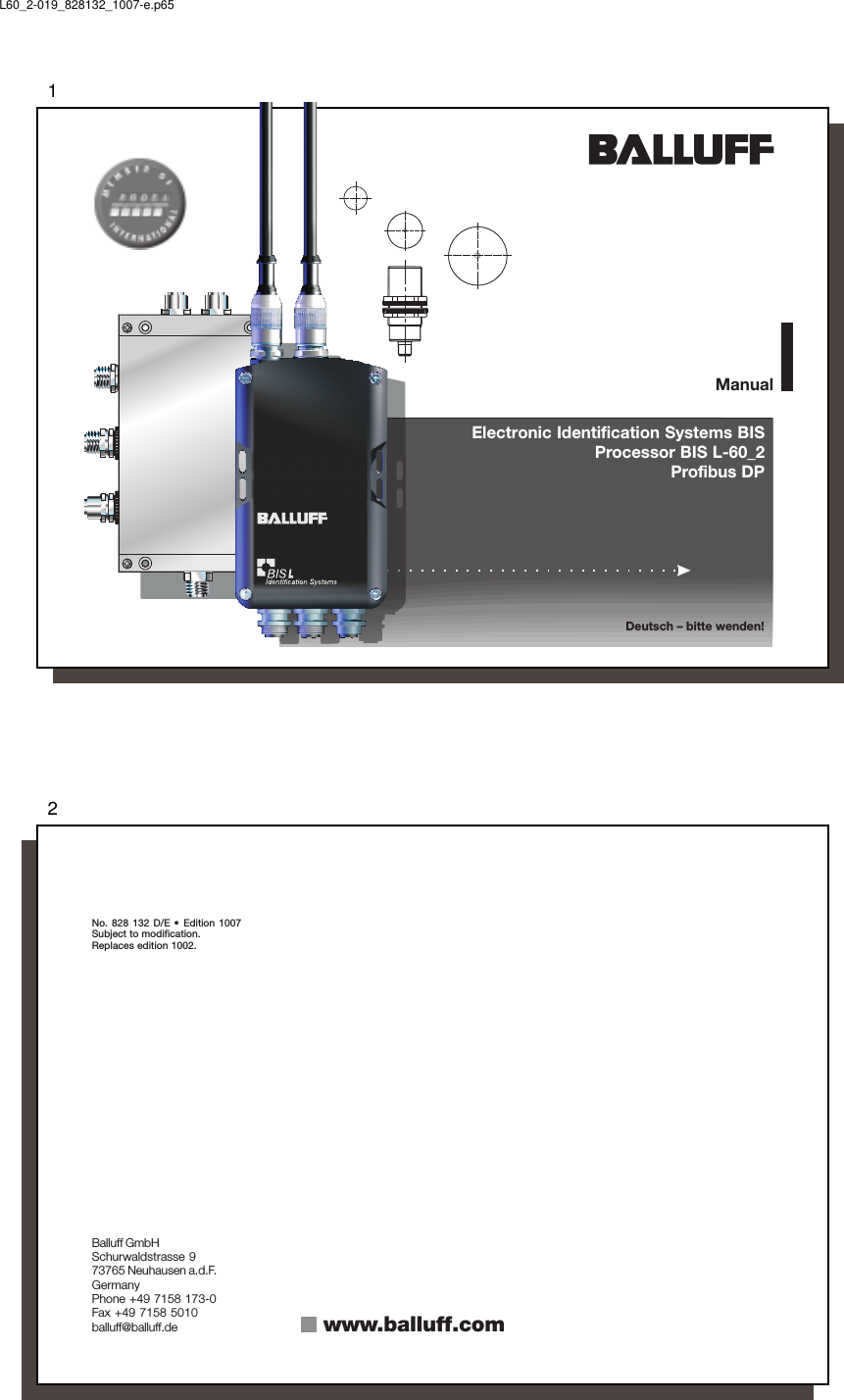
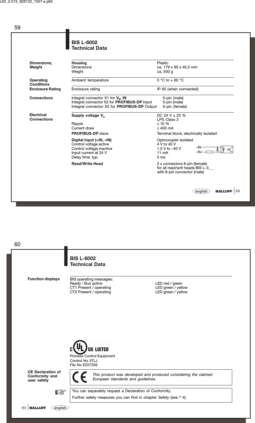
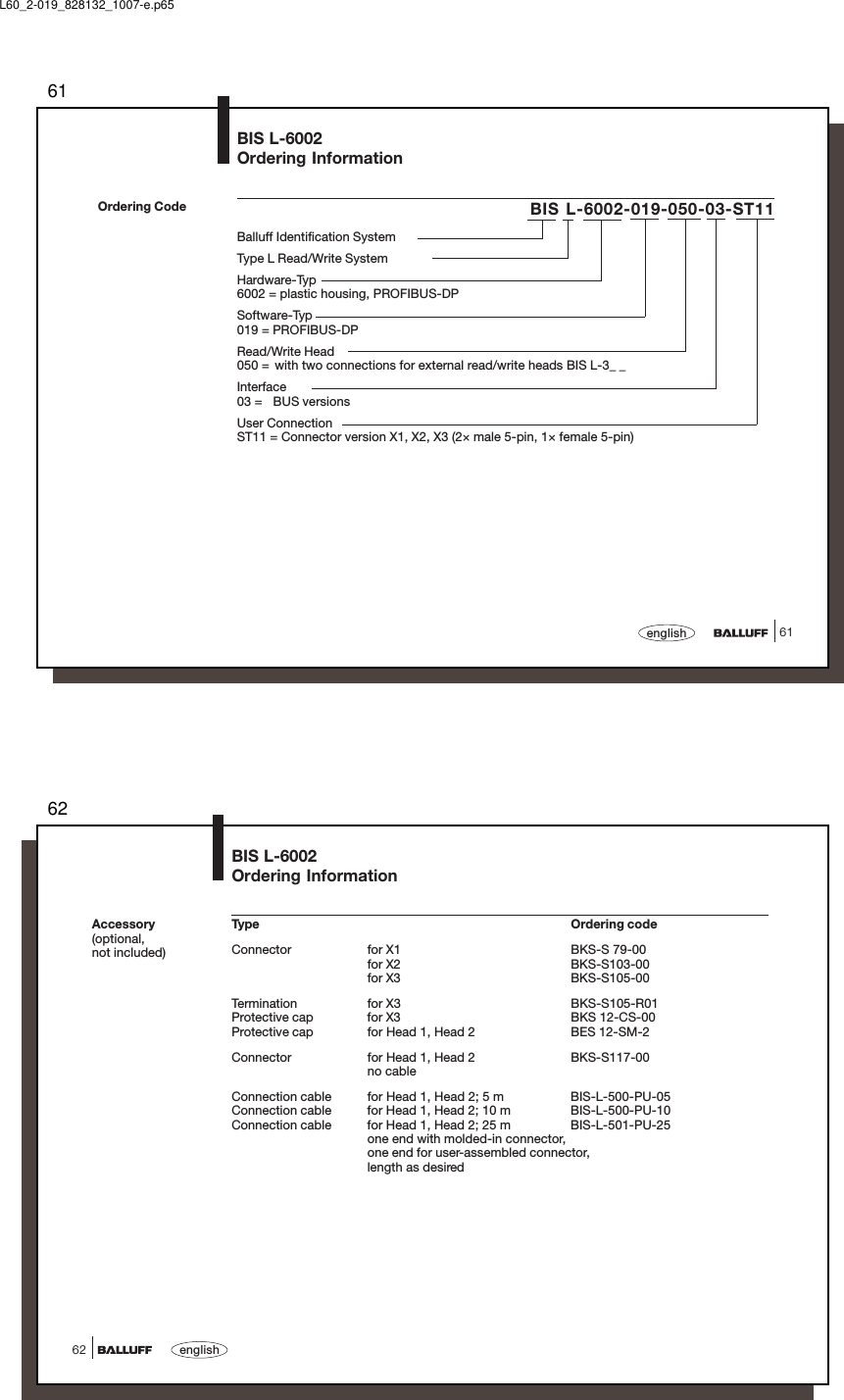
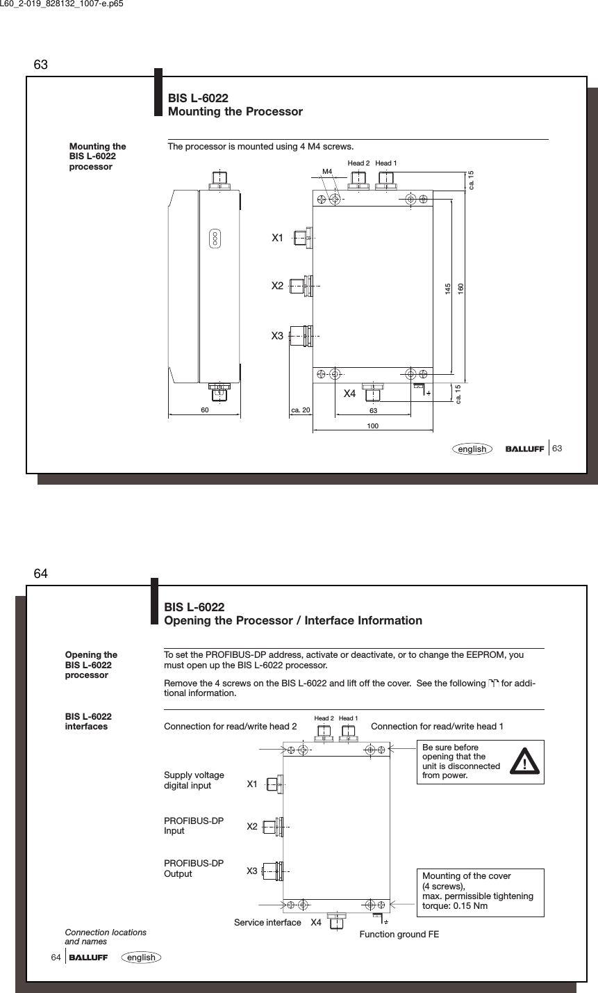
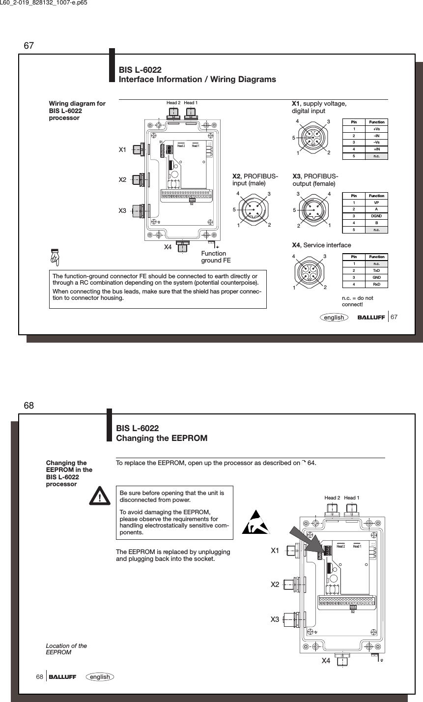
Balluff BISL303 Non-Contact Read/Write System User Manual L60 2 019 828132 1007 e p65

Balluff Inc Non-Contact Read/Write System L60 2 019 828132 1007 e p65

Contents

User Manual (1 of 2).pdf

1Electronic Identification Systems BISProcessor BIS L-60_2Profibus DPManualDeutsch – bitte wenden!L60_2-019_828132_1007-e.p652No. 828 132 D/E •  Edition 1007Subject to modification.Replaces edition 1002.Balluff GmbHSchurwaldstrasse 973765 Neuhausen a.d.F.GermanyPhone +49 7158 173-0Fax +49 7158 5010balluff@balluff.de www.balluff.com
33englishContentsSafety Considerations ................................................................................................................. 4Introduction, BIS L Identification Systems ............................................................................... 5/6BIS L-60_2 Processor, Basic knowledge for application.......................................................... 7/8BUS interface PROFIBUS-DP ................................................................................................ 9-11Function Description: Communication with the processor ................................................ 12Input and Output Buffers ........................................................... 13/14Output Buffer, configuration and explanation ............................ 15-18Input Buffer, configuration and explanation ............................... 19-22Parametering the BIS C-60_2 processor ................................... 23/24Parametering, Parametering Bytes ............................................ 25-27Data-carrier models BIS L-10_-01/L.............................................. 28Data-carrier models BIS L-20_-03/L.............................................. 29Processing data carriers .......................................................... 30-36Examples for protocol sequence ............................................. 37-50Read/Write Times ..................................................................................................................... 51LED Display .............................................................................................................................. 52BIS L-6002 BIS L-6022Mounting the Processor .................................................................................... 53 .................. 63Opening the Processor / Interface Information .................................................54 .................. 64Interface Information / Wiring Diagrams ..................................................... 55-57 ............. 65-67Changing the EEPROM .....................................................................................58 .................. 68Technical Data ............................................................................................. 59/60 ............. 69/70Ordering Information .................................................................................... 61/62 ............. 71/72Symbols / Abbreviations .......................................................................................................... 73Appendix, ASCII Table ............................................................................................................. 74L60_2-019_828132_1007-e.p654english4Safety ConsiderationsSeries BIS L-60_2 processors along with the other BIS L system components comprise anidentification system and may only be used for this purpose in an industrial environment inconformity with Class A of the EMC Law.Installation and operation should be carried out by trained personnel only. Unauthorized workand improper use will void the warranty and liability.When installing the processor, follow the chapters containing the wiring diagrams closely.Special care is required when connecting the processor to external controllers, in particularwith respect to selection and polarity of the signals and power supply.Only approved power supplies may be used for powering the processor. See chapter 'Techni-cal Data' for details.Prevailing safety regulations must be adhered to when using the identification system. Inparticular, steps must be taken to ensure that a failure of or defect in the identification systemdoes not result in hazards to persons or equipment.This includes maintaining the specified ambient conditions and regular testing for functionalityof the identification system including all its associated components.Should there ever be indications that the identification system is not working properly, itshould be taken out of commission and secured from unauthorized use.This manual applies to processors in the series  BIS L-6002-019-050-03-ST11 andBIS L-6022-019-050-03-ST14.Installation andOperationUse and CheckingFault ConditionsScopeApproved Operation
55englishPrinciplesIntroductionBIS L Identification SystemsApplications☞This manual is designed to assist the user in setting up the control program and installing andstarting up the components of the BIS L Identification System, and to assure rapid, trouble-free operation.The BIS L Identification Systems belongs in the category ofnon-contact systems for reading and writing.This dual function permits applications for not only transporting information in fixed-program-med data carriers, but also for gathering and passing along up-to-date information as well.The BIS L identification system allows the use of read-only data carriers.If 2 read/write heads are connected to a BIS L-60_2 processor, both heads can be operatedindependently of each other. This means for example that you can read a data carrier from onehead while writing to another data carrier at the other head.Some of the notable areas of application include– for controlling material flow in production processes(e.g. in model-specific processes),for workpiece conveying in transfer lines,in data gathering for quality assurance,for gathering safety-related data,– in storage systems for monitoring inventory movement;– in transporting and conveying systems.L60_2-019_828132_1007-e.p656english6System Components The main components of the BIS L Identification Systems are:–Processor,–Read/Write Heads and–Data carriersIntroductionBIS L Identification SystemsBIS L-3_ _BIS L-3_ _ BIS L-3_ _BIS L-3_ _PROFIBUS-DPConfiguration withBIS L-6002processorData carriers BIS L-1_ _ and BIS L-2_ _-03/L1)Processor  BIS L-60021) Mixed operation of type BIS L-1_ _ and BIS L-2_ _-03/L together is possibleRead/write headProcessor  BIS L-6022Schematicrepresentation of anIdentification System(example)
77englishSelecting SystemComponentsThe BIS L-6002 processor has a plastic housing.The BIS L-6022 processor has a metal housing.Connection is made through round connectors. Two read/write heads can be cable con-nected.Series BIS L-60_2 processors have in addition a digital input. The input has various functionsdepending on the configuration (see Parametering).The read/write distances depend on which data carriers are used. Additional information on theread/write heads in series BIS L-3_ _ including all the possible data carrier/read-write headcombinations can be found in the manuals for the respective read/write heads.The system components are electrically supplied by the processor. The data carrier representsa free-standing unit and needs no line-carried power. It receives its energy from the read/writehead. The latter constantly sends out a carrier signal which supplies the code head as soon asthe required distance between the two is reached. The read/write operation takes place duringthis phase. Reading and writing may be dynamic or static.BIS L-60_2 ProcessorBasic knowledge for applicationL60_2-019_828132_1007-e.p658english8BIS L-60_2 ProcessorBasic knowledge for applicationThe processor writes data from the host system to the data carrier or reads data from the datacarrier through the read/write head and prepares it for the host system. Host systems mayinclude:–a host computer (e.g. industrial PC) or– a programmable logic controller (PLC)For applications requiring high security against bad data, CRC_16 checking can be used.Here a check code is written to the data carrier which allows the data to be checked forintegrity at any time or location.Advantages to CRC_16: Very high data integrity, even during the non-active phase (datacarrier outside the active zone of the r/w head)Disadvantages to CRC_16: Longer read/write times, some user data space is taken up onthe data carrier.Use of CRC_16 can be parameterized by the user. (see   25)Control FunctionData checking withCRC_16
99englishCommunication between the BIS L-60_2 processor and the host system is via PROFIBUS-DP.The PROFIBUS-DP system consists of the components:– the bus master and– the bus modules/slaves (here the BIS L-60_2 processor).Important hints for use with PLC:In some control systems the PROFIBUS-DP data area is not synchronously transmitted with theupdating of the input/output content. If more than 2 bytes of data are sent, a mechanism mustbe used which guarantees that the data in the PLC and the data in the BIS L are always identi-cal!1st alternative: Synchronous data transmission as a setting on the MasterIn this method the bus Master ensures that all the data necessary for the respective Slave arealways sent contiguously. There is usually a special software function in the PLC which likewisecontrols access between the PLC and bus Master so that data are always sent contiguously.2nd alternative: Set 2nd bit headerData exchange between PLC and BIS is controlled by the so-called bit header. This is alwaysthe first byte of the respective read/write head in the data buffer. This bit header exists both inthe input range (data from BIS to the PLC) and in the output range (data from the PLC to theBIS). lIf this bit header is also sent as the last byte, a comparison of these two bytes can beused to guarantee the consistency of the transmitted data.In this method the PLC cycle is unaffected nor is the bus access time changed. All that isrequired is that a byte in the data buffer be used for the 2nd bit header instead of for user data.This 2nd alternative is the Balluff recommended setting (factory default).PROFIBUS-DP☞BUS interface PROFIBUS-DPL60_2-019_828132_1007-e.p6510english10Station AddressFor the correct parametering of the bus master as per type, CD ROM, containing the unit’smaster data in the form of a GSD file is included with the BIS L-60_2 processor.The Processor BIS L-60_2 is delivered with the station address 126. This has to be set indi-vidually before using in a bus system. See information on   11.An input buffer and an output buffer are used for the data exchange with the control system.The size of these buffers has to be configured via the master.The possible settings are entered in the GSD file (and Type file). A minimum of 4 and a maxi-mum of 128 bytes can be accommodated. However, it must be an even number.Besides, in the case of the BIS L-60_2 processor, there are 6 further bytes (User-ParameterBytes) which have to be set while parametering. The significance of the 6 bytes for para-metering is described starting from   25.The preset is stored in the GSD file.Input/Output BufferUnit's Master DataParametering BytesUser-Parameter BytesBUS interface PROFIBUS-DP☞☞
1111englishStation AddresssettingThe station address under which the unit is accessed on the bus can be assigned through theslide switch S1. Each address shall be assigned only once.The slide switch S1 is binary coded. The setting of the station address is carried out accordingto the scheme shown in the table. Switch position: no = left, yes = right.The address 85 is set in the following figure.no  yesTo open the cover of the processor, see   54 for BIS L-6002 or   64 for BIS L-6022.BUS interface PROFIBUS-DPSlide switch S1(with cover removed)StationAddressSlide switch S17654321262524232221200not allowed1 nonononononoyes2 nononononoyesno3 nononononoyesyes4 nonononoyesnono5 nonononoyesnoyes...85 yes no yes no yes no yes...123 yes yes yes yes no yes yes124 yes yes yes yes yes no no125 yes yes yes yes yes no yes126 yes yes yes yes yes yes no127 not allowedalways on noX1 X2 X3Head1Head21on243on onon67on on5on8ononon onHead 1Head 2S113246 578911121416 15 13 10S21719 18➪L60_2-019_828132_1007-e.p6512english12Function DescriptionCommunication with the processorCommunication between the host system and the processor takes place using a fixed proto-col sequence. Data integrity from the control to the processor and vice-versa is indicated by acontrol bit. This bit is used to implement a handshake between the control and the processor.Following is a simplified representation of the sequence of a job sent from the control to theprocessor:1. The control sends a command designator to the processor together with the associatedcommand parameters and sets a bit (AV bit). This bit indicates to the processor that thetransmitted data are valid and that the job is now beginning.2. The processor takes the job and sets a bit (AA bit), which indicates this to the control.3.  If an additional exchange of data between the control and the processor is required tocarry out the job, each uses a bit (TI bit and TO bit) to indicate that the control / processoris now ready for additional data exchange or has accepted the received data.4. Once the processor has carried out the job correctly, it sets a bit (AE bit).5. Once the control has accepted all the important data, it indicates this to the processor byresetting the bit that was set at the beginning (AV bit).6. The processor now in turn sets all the control bits that were set during the sequence(AA bit, AE bit) and is ready for the next job.Please see also 30...36 and theexamples on 37...50.Basic Procedure
1313englishInput and OutputBuffersIn order to transmit commands and data between the BIS L-60_2 and the host system, thelatter must prepare two fields. These two fields are:–the output bufferfor the control commands which are sent to the BIS Identification System andfor the data to be written.–the input bufferfor the data to be read andfor the designators and error codes which come from the BIS Identification System.The possible setting values are stored in the GSD file.The buffer size can be selected between 4 and 128 bytes in steps of 2 bytes. This must begiven by the master during parametering. The total buffer size is divided into 2 ranges:Buffer range 1 for Read/Write Head 1; size is specified in paramter byte 6.Buffer range 2 for Read/Write Head 2; size = total buffer size – buffer size of Read/WriteHead 1.See   14 for example.If a buffer size of less than 8 bytes is set for a read/write head, a read/write request can becarried out without specifying the start address and the number of bytes. Automatic reading forCodetag-Present (see   31) remains active. This permits fast reading of small data quantitieswithout placing an unnecessary load on the bus.Buffer size – 1 = number of bytes read without double bit header;Buffer size – 2 = number of bytes read with double bit header.☞Function DescriptionInput and Output BuffersPlease note thebasic procedure on 12 and 30...36and the exampleson pages   37...50.L60_2-019_828132_1007-e.p6514english14Function DescriptionInput and Output Buffers☞Example: The 82 bytes for the total buffer need to be distributed. An input/output buffer of46 bytes is assigned to Read/Write Head 1. This results in an input/output buffer of 36 bytesfor Read/Write Head 2.Procedure: The buffer size for Read/Write Head 1 is set to 46 bytes. This means using theparameter byte 6 to enter Hex value 2E (corresponds to 46 decimal), which corresponds tobinary 00101110.PLC Organisation: The buffer range starts at input byte IB 32 and output byte OB 32.Result:Read/Write Head 1: Subaddress 00 IB 32 and OB 32(R/W 1) Input buffer IB 32 to IB 77Output buffer OB 32 to OB 77Read/Write Head 2: Subaddress 00 IB 78 and OB 78(R/W 2) Input buffer IB 78 to IB 113Output buffer OB 78 to OB 113IB 0 / OB 0 PLC bufferBuffer for R/W 1Buffer for R/W 2Input and OutputBuffers(continued)Note that these buffers can be in two differentsequences depending on the type of control.The following description is based on sequence 1!Sequence 1 Sequence 2Subaddress 00 Subaddress 0101 0002 0303 0204 0505 0406 0707 06Please note thebasic procedure on 12 and 30...36and the exampleson pages   37...50.
1515englishConfiguration of theOutput Buffer forOne (1) Read/WriteHeadFunction DescriptionOutput buffer, configuration and explanationDescription ofOutput BufferPlease note thebasic procedure on 12 and 30...36and the exampleson pages   37...50.The last two bytes can be parameterized as the 2nd bit header (default).Bit No.76543210Subaddress00Hex = Bit Header TI KA GR AV Bit Name01Hex Command Designator or Data02Hex Start Address (Low Byte) or Program No. or Data03Hex Start Address (High Byte) or Data04Hex No. of Bytes (Low Byte) or Data05Hex No. of Bytes (High Byte) or Data06Hex Data... DataLast Byte 2nd Bit Header (as above) or DataSub- Bit Meaning Function Descriptionaddress Name00Hex TI Toggle-Bit In Shows during a read action that the controller is readyBit Header for additional data.KA Head function Turn read/write head on/off as needed.Active = 0 Read/write head is on.Inactive = 1 Read/write head is off.GR Ground state Causes the BIS system to go to the ground statefor the respective read/write head.Any pending command is cancelled.AV Command Signals the identification system that a commandfor the respective read/write head is present.(continued next  )L60_2-019_828132_1007-e.p6516english16Sub- Meaning Function Descriptionaddress01Hex Command designator00Hex No command present01Hex Read data carrier02Hex Write to data carrier06HEX Store program in the EEPROM for the Mixed Data Accessfunction07HEX Store the start address for the Auto-Read function in the EEPROM12HEX Initialize the CRC16 data check21HEX Read for Mixed Data Access function(corresponding to the program stored in the EEPROM)22HEX Write for Mixed Data Access function(corresponding to the program stored in the EEPROM)or: Data for writing to the data carrieror: Program data for writing to the EEPROM.(continued next  )Function DescriptionOutput buffer, configuration and explanationDescription ofOutput Buffer(continued)Please note thebasic procedure on 12 and 30...36and the exampleson pages   37...50.
1717englishFunction DescriptionOutput buffer, configuration and explanationPlease note thebasic procedure on 12 and 30...36and the exampleson pages   37...50.Description ofOutput Buffer(continued)Sub- Meaning Function Descriptionaddress02Hex Start address Address at which reading from or writing to the data carrier begins.(Low Byte) (The Low Byte includes the address range from 0 to 255).or: Start address Address for the Auto-Read function, starting at which the code(Low Byte) tag is to be read. The value is stored in the EEPROM. (The LowByte covers the address range from 0 to 255).or: Program No. Number of the program to be stored in the EEPROM inconjunction with command ID 06Hex for Mixed Data Accessfunction (values between 01Hex and 0AHex are allowed!).or: Program No. Number of the program stored in the EEPROM for read or writeoperations in conjunction with command ID 22Hex or 22Hex for theMixed Data Access function.or: Data for writing to the data carrieror: Program data for writing to the EEPROM.03Hex Start address Address for reading from or writing to the data carrier .(High Byte) (The High Byte includes the address range from 256 to 1999).or: Start address Address for the Auto-Read function, starting at which the code(High Byte) tag is to be read. The value is stored in the EEPROM.(The High Byte includes the address range from 256 to 1999).or: Data for writing to the data carrieror: Program data for writing to the EEPROM.(continued next  )L60_2-019_828132_1007-e.p6518english18Function DescriptionOutput buffer, configuration and explanationPlease note thebasic procedure on 12 and 30...36and the exampleson pages   37...50.Description ofOutput Buffer(continued)Sub- Meaning Function Descriptionaddress04Hex No. of bytes Number of bytes to read or write beginning with the start address(Low Byte) (the Low Byte includes from 1 to 255 bytes).or: Data for writing to the data carrieror: Program data for writing to the EEPROM.05Hex No. of bytes Number of bytes to read or write beginning with the start address(High Byte) (the High Byte includes the address range from 256 to 1999).or: Data for writing to the data carrieror: Program data for writing to the EEPROM.06Hex Data for writing to the data carrieror: Program data for writing to the EEPROM.... Data for writing to the data carrieror: Program data for writing to the EEPROM.Last byte2nd Bit header The data are valid if the 1st and 2nd bit header are identical.or: Data for writing to the Data carrieror: Program data for writing to the EEPROM.
1919englishFunction DescriptionInput buffer, configuration and explanationConfiguration of theinput buffer for one(1) read/write headThe last byte can be arranged as a 2nd bit header through parametering (default).Bit No.76543210Subaddress00Hex = Bit Header BB HF TO IN AF AE AA CP Bit Name01Hex Error Code or Data02Hex Data03Hex Data04Hex Data05Hex Data06Hex Data... DataLast byte 2nd Bit Header (as above) or DataSub- Bit Meaning Function Descriptionaddress Name00Hex BB Ready The BIS Identification System is in the Ready state.Bit Header HF Head Error Cable break from read/write head orno read/write head connected.TO Toggle-Bit Out for read: BIS has new/additional data ready.for write: BIS is ready to accept new/additional data.(continued on next  )Description ofInput BufferPlease note thebasic procedure on 12 and 30...36and the exampleson pages   37...50.L60_2-019_828132_1007-e.p6520english20Function DescriptionInput buffer, configuration and explanationDescription ofInput Buffer(continued)Sub- Bit Meaning Function Descriptionaddress Name00Hex (continued)Bit Header IN Input If the parameter "Input IN" is 1, this bit indicatesthe state of the Input.AF Command Error The command was incorrectly processed or aborted.AE Command end The command was finished without error.AA Command start The command was recognized and started.CP Codetag Present Data carrier present within the active zone of theread/write head.In addition to the CP bit, the output signal CT present is available. Thisallows you to process the presence of a data carrier directly as a hardwaresignal.Sub- Meaning Function Descriptionaddress01Hex Error code Error number is entered if command was incorrectly processedor aborted.  Only valid with AF bit!00Hex No error.01Hex Reading or writing not possible because no data carrier is presentin the active zone of a read/write head.02Hex Read error.03Hex Data carrier was removed from the active zone of the read/writehead while it was being read.04Hex Write error.(continued on next  )Please note thebasic procedure on 12 and 30...36and the exampleson pages   37...50.
2121englishFunction DescriptionInput buffer, configuration and explanationSub- Meaning Function Descriptionaddress01Hex Error code (continued)05Hex Data carrier was removed from the active zone of the read/writehead while it was being written.07Hex AV bit is set but the command designator is missing or invalid.                  or: Number of bytes is 00Hex.09Hex Cable break to select read/write head, or head not connected.0CHex The EEPROM cannot be read/programmed.0DHex Communication with the read/write head.0EHex The CRC of the read data does not coincide with the CRC ofthe data carrier.0FHex Contents of the 1st and 2nd bit header (1st and last bytes) ofthe output buffers are not identical (2nd bit header must beserved).20Hex Adressing of the read/write job is outside the memory range ofthe data carrier.21Hex Function invoked which is not possible for the data carriercurrently in front of the read/write head.or: Data Data which was read from the data carrier.(continued next  )Description ofInput Buffer(continued)Please note thebasic procedure on 12 and 30...36and the exampleson pages   37...50.L60_2-019_828132_1007-e.p6522english22Function DescriptionInput buffer, configuration and explanationSub- Meaning Function Descriptionaddress02Hex Data Data which was read from the data carrier.... Data Data which was read from the data carrier.Last byte2nd Bit header The data are valid if the 1st and 2nd bit headers are inagreement.or: Data Data which was read from  the data carrier.Description ofInput Buffer(continued)Please note thebasic procedure on 12 and 30...36and the exampleson pages   37...50.
2323englishFunction DescriptionParametering the BIS L-60_2 processorParameters,OverviewThere are 6 user parameter bytes stored on the Profibus master that can be used to activateand deactivate various functions. Setting is done directly by linking a device to the Profibusmaster. The parameter default settings are stored in the GSD file.– CRC_16 data check:If this function is activated, the correctness of the read or written data is ensured by aCRC_16 data check (see   8).– Dynamic operation on read/write head 1 or 2:If dynamic operation is parametered, a read/write job can be sent even though there is noData carrier in the active zone of the head. As soon as a Data carrier passes by the head,the command is immediately carried out.– "Auto-Read” for read/write head 1 or 2:If this function is activated, the processor reads out the first (max. 31) bytes from the Datacarrier starting at a defined start address as soon as the tag enters the active zone of theread/write head. The start address must first have been stored in the processor’s EEPROMwith the command ID 07Hex.– 2nd bit header at end of in- and output buffer:The 2nd bit header (factory setting) prevents data from being accepted by the bus as longas it is not fully updated.– Display state of the digital input in the bit header of the input buffer:If this function is activated, the IN-bit displays the state of the digital input of the processor:IN = 0 → digital input low; IN = 1 → digital input highPlease note thebasic procedure on 12 and 30...36and the exampleson pages   37...50.L60_2-019_828132_1007-e.p6524english24Function DescriptionParametering the BIS L-60_2 processorParameters,Overview(continued)– Reset BIS L-60_2 processor through the digital input:If this function is activated, the processor is reset when the digital input is set to high.– Selecting the data carrier type for processing:Depending on the selection, either all or only specified data carriers may be processed.– Output data carrier model and serial number:If this function is activated, at CT Present the data carrier model and serial number (UID =unique ID) are output.At data carrier model BIS L-1_ _-01 the serial number is 4 bytes. At all other data carriermodels the serial number is 8 bytes.If this function is activated and dynamic mode is not set, no read data are output atCT Present, but rather only the model and UID.Please note thebasic procedure on 12 and 30...36and the exampleson pages   37...50.☞
2525englishParametering BytesUser-Parameter BytesFor parametering all 6 bytes must always be transferred in Hex. Only the bits men-tioned may be changed. No guaranty will be given for the proper functioning of theBIS L-60_2 if any of the other bits are changed.The default values (factory setting) for the 6 bytes are:1st byte 2nd byte 3rd byte 4th byte 5th byte 6th byteHEX 00 80 00 82 00 02Binary 00000000 10000000 00000000 10000010 00000000 00000010       bit 4 bit 1...8   bit 7    bit 1       bit 4 bit 1...8      bit 5       bit 5 bit 8    bit 2       bit 5The bits which serve for parametering have the following functions:1st byte, bit 5, Activate CRC_16 data checking2nd byte, bit 5, Dynamic mode on read/write head 1(for effects on read/write times, see   51)2nd byte, bit 4, Activate Auto-Read function starting at specified address after CT presentfor Head 1 (the number of bytes read depends on the selected buffer sizeminus bit headers for Head 1)3nd byte, bit 1...8 Select data-carrier model for processing:00Hex: All data-carrier modelsFEHex: Mifare: All Mifare data carriers supported by Balluff.FFHex: ISO15693: All ISO15693 data carriers supported by Balluff.Function DescriptionParametering, Parametering BytesBit state: 0 = no1 = yesThese are used forconfiguration:Having the followingfunctions:Please note thebasic procedure on 12 and 30...36and the exampleson pages   37...50.L60_2-019_828132_1007-e.p6526english264th byte, bit 8, Arrange a 2nd bit header at the end of the input and output  buffersIf this function is selected, then the minimum size of both buffers is 4 words (8 bytes) each.4th byte, bit 7, Display state of the digital input in the bit header of the input buffers:0 = no1 = yes Input is Low: "IN" in the bit header of the input buffers = 0.Input is High: "IN" in the bit header of the input buffers = 1.4th byte, bit 2, Reset the BIS L-60_2 processor through the digital input:0 = no1 = yes Input is Low: Do not reset.Input is High: Reset.4th byte, bit 1, Output data-carrier model and serial number at CT present:0 = no At CT present the first data carrier data are output on Profibus.1 = yes At CT present the data carrier model and serial number (UID = unique ID)are output on Profibus. A distinction is made between type 01 with a4-byte UID and type 03 with a 5-byte UID.5th byte, bit 5 Dynamic mode on read/write head 2(for effects on read/write times, see   51)5th byte, bit 4 Activate Auto-Read function for Head 2 starting at specified address afterCT present (the number of bytes read depends on the selected buffer sizeminus bit headers for Head 2)Parametering BytesUser-Parameter Bytes(continued)Function DescriptionParametering, Parametering BytesBit state: 0 = no1 = yesPlease note thebasic procedure on 12 and 30...36and the exampleson pages   37...50.
2727english6th byte, bit 1...6 No. of bytes in input and output buffer which shall be used forread/write head 1, see example on   16The specification for the input and output buffer on the Master applies to both read/writeheads, i.e. this buffer must be divided for both heads. The specification is done in Hex formatand must be in a range between 02Hex and 80Hex (128 dec.).If only one read/write head (Head 1) will be used, you may enter the same value here as for thetotal buffer size. An entry of less than 2 bytes results in an undefined state.Please note the basic procedure on   12 and 30...36 and the examples on pages   37...50.Parametering BytesUser-Parameter Bytes(continued)Function DescriptionParametering, Parametering Bytes☞L60_2-019_828132_1007-e.p6528english28Data-carrier modelsBIS L-10_-01/LCT presentModel BIS L-10_-01/L data carriers have a memory capacity of 192 bytes of user data.These data can be read or programmed. These data carriers also have a unique, 4-byteserial number, which is read-only.The data carrier also contains additional memory ranges for configuration and protecteddata. These areas cannot be processed using the BIS L-60_2 processor.Model BIS L-10_-01/L data carriers are supplied with FFHex 37Hex configuration. Only datacarriers having this configuration are processed.At CT Present the first user data are read from the data carrier and stored in the Profibusinput buffer (see   31). If the “Output data-carrier model and serial number at CT present”function is enabled, model 01Hex is output in Byte 1 of the input buffer and then the 4 bytesrepresenting the unique serial number.The full command set of the BIS L-60_2 processor can be used with model BIS L-10_01/Ldata carriers.When using model BIS L-10_-01/L data carriers, the device parameterizing dependsmainly on the number of bytes to be read and programmed per head.Please refer to   13ff and   23ff.FunctionsDevice parameters☞Data carrierBIS L-10_-01/L
2929englishData-carrier modelsBIS L-20_-03/LCT presentModel BIS L-20_-03/L data carriers have a unique serial number consisting of 5 bytes. Theseare read-only and are considered like user data.At CT Present the 5 bytes of the serial number are read from the data carrier and stored in theProfibus input buffer (see   31). If the “Output data-carrier model and serial number at CTpresent” function is enabled, model 03Hex is output in Byte 1 of the input buffer and then the5 bytes representing the unique serial number.With model BIS L-20_-03/L data carriers, all data are read and output as soon as CT presentoccurs. No other BIS L-60_2 processor commands are usable.When using model BIS L-20_-03/L data carriers, set the following parameters:Total buffer size on Profibus: 16 bytes (8 bytes if only one read/write head is used)Parameterizing bytes: 00Hex 80Hex 00Hex 82Hex 00Hex 08Hexor: 00Hex 80Hex 03Hex 82Hex 00Hex 08Hex→ only model BIS L-20_-03/L data carriers are processed.00Hex 80Hex 00Hex 83Hex 00Hex 08Hex→ output data carrier model and serial number at CT present.FunctionsDevice parametersData carrierBIS L-20_-03/LL60_2-019_828132_1007-e.p6530english30Function DescriptionProcessing data carriersReading and writing To carry out a read or write job, the data carrier must be located in the active zone of theread/write head.A read/write job has the following sequence (see examples on   37ff):1. The host sends to the output buffer:– the command designator to subaddress 01Hex,– the start address for reading or writing to subaddress 02HEX/03HEX,– the number of bytes for reading or writing to subaddress 04HEX/05HEX,– and sets the AV bit in the bit header to high.2. The processor:– takes the request (AA in the bit header of the input buffer to high),– begins to transport the data;read = from data carrier to input buffer,write = from output buffer to data carrier.(Larger data quantities are sent in blocksblock size with 2nd bit header = buffer size - 2,block size without 2nd bit header = buffer size - 1).The toggle bits in the two bit headers are used as a kind of handshaking between thehost and the BIS L-60_2 processor.3. The processor has processed the command correctly (AE bit in the bit header of the inputbuffer). If an error occurred during execution of the command, an error number will bewritten to subaddress 01Hex of the input buffer and the AF bit in the bit header of the inputbuffer will be set.
3131englishStart address forAuto-ReadFunction DescriptionProcessing data carriersCodetag Present(CP bit)As soon as the data carrier enters the active one of the read/write head, the processor indi-cates this by setting the CP bit (Codetag Present).To accelerate the reading of small amounts of data, the ID system makes the first bytes of thedata carrier available in the input buffer of the respective read/write head as soon as the tag isdetected. The number of bytes sent corresponds to the configured buffer size – 1 byte (2 bytesfor 2nd bit header).If a model BIS L-20_-03L is present at the read/write head, a maximum of 5 bytes are output.If the parameter “Output data-carrier model and serial number at CT Present” is set, thedata-carrier model and unique serial number are output instead of the read data. For modelBIS L-20_-03/L data carriers the read data correspond to the serial number.The data are only valid after the rising edge of the CP bit in the bit header of the input buffer.They remain valid until the falling edge of the CP bit, or until the controller issues a new job.If the Auto-Read function is activated, the data are read starting with a specified start addressas soon as the data carrier is recognized. The rising edge of the CP bit is used to providethese data in the input buffer. The start address must be specified for each head usingcommand identifier 07Hex the start addresses may be different. The number of bytes read isdetermined by the selected size of the input buffer, which is distributed over both heads when2 are used.☞L60_2-019_828132_1007-e.p6532english32Function DescriptionProcessing data carriersReading and writingin dynamic modeIn normal operation a read/write job is rejected by the BIS L-60_2 processor by setting theAF bit and an error number if there is no data carrier in the active zone of the read/write head.If dynamic mode is configured, the processor accepts the read/write job and stores it. When adata carrier is recognized, the stored job is carried out.Reading without simultaneous data transmission: In the case of a read job the processorfirst reads our all requested data from the data carrier after receiving the start address and thedesired number of bytes, and then sets the AE bit. Then the data read from the data carrierare written to the input buffer. In the case of larger data amounts this is done in blocks,controlled by the handshake with the toggle bits as described on   30.Reading with simultaneous data transmission: In the case of a read job the processorbegins by transmitting the data into the input buffer as soon as the first 30 bytes (with 2nd bitheader, or 31 bytes without 2nd bit header, or less if the buffer size was set smaller) have beenread from the data carrier beginning with the start address, and indicates this by inverting theTO bit. As soon as the controller inverts the TI bit, the processor sends the data, which havein the meantime been read, to the input buffer. This is repeated until the processor has readout all the desired data from the data carrier. Now the processor sets the AE bit and outputsthe remaining data on the input buffer.Writing without simultaneous data transmission: In the case of a write job the processorwaits until it has received all the data that need to be written from the controller. Only then arethe data written to the data carrier as described on   30.Writing with simultaneous data transmission: In the case of a write job the processorbegins to write the data to the data carrier as soon as it has received the first data to bewritten from the controller’s output buffer. Once all the data have been written to the datacarrier, the AE bit is set.Reading and writingwith simultaneousdata transmission
3333englishMixed Data AccessFunction DescriptionProcessing data carriersSmall read/write programs can be stored in the BIS L-60_2 processor’s EEPROM.The Mixed Data Access function is useful when the required information is stored on the datacarrier at various addresses. This function makes it possible to read out this “mixed”, i.e. non-contiguously stored data from the data carrier in a single procedure and using just one com-mand.Up to 10 programs with up to 25 instructions can be stored. Each program instruction con-tains a “start address” and a “number of bytes” specification. The amount of data for readingmay not exceed 2 kB.Storing a program:The command identifier 06Hex is used to send the read/write program to the BIS L-60_2processor. One program per command can be stored. All 25 program records plus an addi-tional 2 bytes with FFHexFFHex as a terminator must always be sent. This means a total of104 bytes of information per program must be sent (including the command identifier andprogram number).The individual program records must all be contiguous. They must be sent one after the otherand be terminated with FFHexFFHex as a terminator. It is recommended that the remaining, un-used memory sector be filled with FFHexFFHex.If an address range is selected twice, the data will also be output twice.☞L60_2-019_828132_1007-e.p6534english34Mixed Data Access(continued)The following shows the structure of a program:Program structure Subaddress Value RangeCommand designator 01Hex 06Hex1. Program recordProgram number 02Hex 01Hex 01Hex to 0AHex1st data record:Start address Low Byte 03HexStart address High Byte 04HexNumber of bytes Low Byte 05HexNumber of bytes High Byte 06Hex2nd data record:...25th data record:Start address Low Byte 03HexStart address High Byte 04HexNumber of bytes Low Byte 05HexNumber of bytes High Byte 06HexTerminator FFHex FFHexTo store a second program, repeat this process.The procedure for writing these settings to the EEPROM is described in the 7th example on 45...47.Replacing the EEPROM is described on   58 for BIS L-6002 and on   68 for BIS L-6022.Function DescriptionProcessing data carriers
3535englishFunction DescriptionProcessing data carriersRead from datacarrier, with programMixed Data AccessWrite to data carrier,with program MixedData AccessThe command identifier 21Hex can be used to read out the program records stored in theprogram from the data carrier. The user must document exactly which data are to be readfrom where and with what number of bytes for the respective program (see example 8 on   48)The command identifier 22Hex can be used to write the program records stored in the programto the data carrier. The user must document exactly which data are to be written from whereand with what number of bytes for the respective program (see example 9 on   49)To be able to use the CRC_16 check, the data carrier must first be initialized with thecommand identifier 12Hex (see   37). The CRC_16 initialization is used like a normal write job.The latter is rejected (with an error message) if the processor recognizes that the data carrierdoes not contain the correct CRC_16 checksum. Data carriers as shipped from the factory(all data are 0) can immediately be written with CRC-checked data.If CRC_16 data checking is activated, a special error message is output to the interfacewhenever a CRC_16 error is detected.If the error message is not caused by a failed write request, it may be assumed that one ormore memory cells on the data carrier is defective. That data carrier must then be replaced.If the CRC error is however due to a failed write request, you must reinitialize the data carrierin order to continue using it.CRC_16 initializationL60_2-019_828132_1007-e.p6536english36Data-carrier modelsBIS L-10_-01/LCT presentModel BIS L-10_-01/L data carriers have a memory capacity of 192 bytes of user data.These data can be read or programmed. These data carriers also have a unique, 4-byteserial number, which is read-only.The data carrier also contains additional memory ranges for configuration and protecteddata. These areas cannot be processed using the BIS L-60_2 processor.Model BIS L-10_-01/L data carriers are supplied with FFHex 37Hex configuration. Only datacarriers having this configuration are processed.At CT Present the first user data are read from the data carrier and stored in the Profibusinput buffer (see   31). If the “Output data-carrier model and serial number at CT present”function is enabled, model 01Hex is output in Byte 1 of the input buffer and then the 4 bytesrepresenting the unique serial number.The full command set of the BIS L-60_2 processor can be used with model BIS L-10_01/Ldata carriers.When using model BIS L-10_-01/L data carriers, the device parameterizing dependsmainly on the number of bytes to be read and programmed per head.Please refer to   13ff and   23ff.FunctionsDevice parameters☞Data carrierBIS L-10_-01/L
3737englishExample No. 1For configuring withdouble bit headerand 8-byte buffersize!... To be continueduntil the completememory range iswritten. See next  .Function DescriptionExamples for protocol sequenceInitializing the data carrier for the CRC_16 data checkingThe processing of this command is similar to a write command. Start address and number ofbytes have to correspond to the maximum number of data to be used.In this example the complete memory range of a data carrier with 192 bytes shall be used(BIS L-10 _-01/L). Because 2 bytes are used for the CRC only 168 bytes can be used as databytes, hence: start address = 0, number of bytes = 168.5.) Process subaddresses of the output buffer:BIS L-60_2 Identification System:2.) Process subaddresses of the input buffer in theorder shown:3.) Process subaddresses of the output buffer: 4.) Process subaddresses of the output buffer:6.) Process subaddresses of the output buffer:Host:1.) Process subaddresses of the output buffer in theorder shown:00Hex/07Hex Set AA-Bit, invert TO-Bit01Hex Command designator 12Hex02Hex Start address 00Hex03Hex Start address 00Hex04Hex No. of bytes 92Hex05Hex No. of bytes 02Hex00Hex/07Hex Set AV-Bit01...06Hex Enter first 6 bytes of data00Hex/07Hex Invert TI-Bit01...06Hex Enter the second 6 data bytes00Hex/07Hex Invert TI-Bit01...06Hex Copy first 6 data bytes      Process subaddress of the input buffer:00Hex/07Hex Invert TO-Bit01...06Hex Copy second 6 data bytes     Process subaddress of the input buffer:00Hex/07Hex Invert TO-BitL60_2-019_828132_1007-e.p6538english38Example No. 1(continued)For configuring withdouble bit headerand 8-byte buffersize!Function DescriptionExamples for protocol sequenceHost: BIS L-60_2 Identification System:9.) Process subaddresses of the output buffer: 10.)Process subaddresses of the input buffer:7.) Process subaddresses of the output buffer: 8.) Process subaddresses of the output buffer:01...06Hex Enter the remaining data byte00Hex/07Hex Invert TI-Bit00Hex/07Hex Reset AV-Bit01...06Hex Copy the remaining data byte      Process subaddress of the input buffer:00Hex/07Hex Set AE-Bit00Hex/07Hex Reset AA-Bit and AE-Bit
3939englishFunction DescriptionExamples for protocol sequenceRead 17 bytes starting at data carrier address 10 (data carrier type BIS L-10 _-01/L):Example No. 2For configuring withdouble bit headerand 8-byte buffersize!7.) Process subaddresses of the input buffer: 8.) Process subaddresses of the input buffer:BIS L-60_2 Identification System:2.) Process subaddresses of the input buffer in theorder shown:3.) Process subaddresses of the input buffer: 4.) Process subaddresses of the input buffer:6.) Process subaddresses of the input buffer:5.) Process subaddresses of the input buffer:Host:1.) Process subaddresses of the output buffer in theorder shown:01Hex Command designator 01Hex02Hex Start address Low Byte 0AHex03Hex Start address High Byte 00Hex04Hex No. of bytes Low Byte 11Hex05Hex No. of bytes High Byte 00Hex00Hex/07Hex Set AV-Bit00Hex/07Hex Set AA-Bit01...06Hex Enter first 6 bytes of data00Hex/07Hex Set AE-Bit01...06Hex Copy first 6 data bytes      Process subaddress of the output buffer:00Hex/07Hex Invert TI-Bit01...06Hex Enter the second 6 data bytes00Hex/07Hex Invert TO-Bit01...06Hex Copy second 6 data bytes     Process subaddress of the output buffer:00Hex/07Hex Invert TI-Bit01...05Hex Enter the remaining 5 data bytes00Hex/07Hex Invert TO-Bit01...05Hex Copy the remaining 5 data bytes      Process subaddress of the output buffer:00Hex/07Hex Reset AV-Bit00Hex/07Hex Reset AA-Bit and AE-BitL60_2-019_828132_1007-e.p6540english40Function DescriptionExamples for protocol sequenceRead 17 bytes starting at data carrier address 10, with simultaneous data transmission(data carrier type BIS L-10 _-01/L):While the read job is being carried out and as soon as the input buffer is filled, the first dataare sent. The AE bit is not set until the “Read” operation is completed by the processor.The reply “Job End” = AE bit is reliably set no later than before the last data are sent. Theexact time depends on the requested data amount, the input buffer size and the timing of thecontroller. This is indicated in the following by the note Set AE-Bit (in italics).01Hex Command designator 01Hex02Hex Start address Low Byte 0AHex03Hex Start address High Byte 00Hex04Hex No. of bytes Low Byte 11Hex05Hex No. of bytes High Byte 00Hex00Hex/07Hex Set AV-Bit00Hex/07Hex Set AA-Bit01...06Hex Enter first 6 bytes of data00Hex/07Hex Invert TO-Bit00Hex/07Hex Set AE-Bit01...06Hex Enter the second 6 data bytes00Hex/07Hex Invert TO-Bit00Hex/07Hex Set AE-Bit01...06Hex Copy first 6 data bytes      Process subaddress of the output buffer:00Hex/07Hex Invert TI-BitExample No. 3like 2nd example butwith simultaneousdata transmissionFor configuring withdouble bit headerand 8-byte buffersize!Continued on next  .BIS L-60_2 Identification System:2.) Process subaddresses of the input buffer in theorder shown:Host:1.) Process subaddresses of the output buffer in theorder shown:3.) Process subaddresses of the input buffer: 4.) Process subaddresses of the input buffer:
4141englishFunction DescriptionExamples for protocol sequenceHost: BIS L-60_2 Identification System:01...05Hex Enter the remaining 5 data bytes00Hex/07Hex Invert TO-Bit00Hex/07Hex Set AE-BitExample No. 3(continued)like 2nd example butwith simultaneousdata transmissionFor configuring withdouble bit headerand 8-byte buffersize!7.) Process subaddresses of the input buffer: 8.) Process subaddresses of the input buffer:6.) Process subaddresses of the input buffer:5.) Process subaddresses of the input buffer:01...06Hex Copy second 6 data bytes     Process subaddress of the output buffer:00Hex/07Hex Invert TI-Bit01...05Hex Copy the remaining 5 data bytes      Process subaddress of the output buffer:00Hex/07Hex Reset AV-Bit00Hex/07Hex Reset AA-Bit and AE-BitL60_2-019_828132_1007-e.p6542english42Function DescriptionExamples for protocol sequenceExample No. 4For configuring withdouble bit headerand 8-byte buffersize!Read 30 bytes starting at data carrier address 10 with read error(data carrier type BIS L-10 _-01/L):Host:1.) Process subaddresses of the output buffer in theorder shown:BIS L-60_2 Identification System:2.) Process subaddresses of the input buffer in theorder shown:If an error occurs right away:3.) Process subaddress of the input buffer: 4.) Process subaddresses of the input buffer:01Hex Command designator 01Hex02Hex Start address Low Byte 0AHex03Hex Start address High Byte 00Hex04Hex No. of bytes Low Byte 1EHex05Hex No. of bytes High Byte 00Hex00Hex/07Hex Set AV-Bit00Hex/07Hex Set AA-Bit01Hex Enter error number00Hex/07Hex Set AF-Bit01Hex Copy error number      Process subaddress of the output buffer:00Hex/07Hex Reset AV-Bit00Hex/07Hex Reset AA-Bit and AE-Bit
4343englishFunction DescriptionExamples for protocol sequenceExample No. 5For configuring withdouble bit headerand 8-byte buffersize!Write 16 bytes starting at data carrier address 20 (data carrier type BIS L-10 _-01/L):Host:1.) Process subaddresses of the output buffer in theorder shown:BIS L-60_2 Identification System:2.) Process subaddresses of the input buffer in theorder shown:3.) Process subaddresses of the output buffer: 4.) Process subaddresses of the output buffer:9.) Process subaddresses of the output buffer: 10.)Process subaddresses of the input buffer:5.) Process subaddresses of the output buffer: 6.) Process subaddresses of the output buffer:7.) Process subaddresses of the output buffer: 8.) Process subaddresses of the output buffer:01Hex Command designator 02Hex02Hex/03Hex Start address 14Hex / 00Hex04Hex/05Hex No. of bytes 10Hex / 00Hex00Hex/07Hex Set AV-Bit00Hex/07Hex Set AA-Bit, invert TO-Bit01...06Hex Enter the first 6 data bytes00Hex/07Hex Invert TI-Bit01...06Hex Copy first 6 data bytes      Process subaddress of the input buffer:00Hex/07Hex Invert TO-Bit01...06Hex Enter the second 6 data bytes00Hex/07Hex Invert TI-Bit01...06Hex Copy second 6 data bytes     Process subaddress of the input buffer:00Hex/07Hex Invert TO-Bit01...04Hex Enter the remaining 4 data bytes00Hex/07Hex Invert TI-Bit01...04Hex Copy the remaining 4 data bytes     Process subaddress of the input buffer:00Hex/07Hex Set AE-Bit00Hex/07Hex Reset AV-Bit 00Hex/07Hex Reset AA-Bit and AE-BitL60_2-019_828132_1007-e.p6544english44Example No. 6Address assignmentfor the Auto-ReadfunctionFor configuring withdouble bit headerand 8-byte buffersize!Programming start address 75:01Hex Command designator 07Hex02Hex Start address Low Byte 4BHex03Hex Start address High Byte 00Hex00Hex/07Hex Set AV-Bit00Hex/07Hex Set AA-Bit and AE-BitTo ensure correct data output, use command identifier 07Hex for each distributed buffer Head 1and/or Head 2.If the Auto-Read function is not activated, the processor runs in standard mode and sendsstarting with data carrier address 0 until the buffer is filled.☞Host:1.) Process subaddresses of the output buffer in theorder shown:BIS L-60_2 Identification System:2.) Process subaddresses of the input buffer:3.) Process subaddresses of the output buffer: 4.) Process subaddresses of the input buffer:00Hex/07Hex Reset AV-Bit 00Hex/07Hex Reset AA-Bit and AE-BitFunction DescriptionExamples for protocol sequence
4545englishFunction DescriptionExamples for protocol sequenceExample No. 7Store Mixed DataAccess programFor configuring withdouble bit headerand 8-byte buffersize!Storing a program for reading out 3 data records:1st data record Start address  5 Number of bytes 72nd data record Start address  75 Number of bytes 33rd data record Start address  112 Number of bytes 17Total number of bytes exchanged in the operation: 27 bytesAll 104 bytes are written for the programming.Host:1.) Process subaddresses of the output buffer in theorder shown:BIS L-60_2 Identification System:2.) Process subaddresses of the input buffer:01Hex Command designator 06Hex02Hex Program number 01Hex00Hex/07Hex Set AV-Bit00Hex/07Hex Set AA-Bit, invert TO-Bit3.) Process subaddresses of the output buffer: 4.) Process subaddresses of the input buffer:01Hex 1st start address (Low Byte) 05Hex02Hex (High Byte) 00Hex03Hex 1st number ofbytes(Low Byte) 07Hex04Hex (High Byte) 00Hex05Hex 2nd start address (Low Byte) 4BHex06Hex (High Byte) 00Hex00Hex/07Hex Invert TI-Bit00Hex/07Hex Invert TO-BitContinued on next  .L60_2-019_828132_1007-e.p6546english46Function DescriptionExamples for protocol sequenceHost: BIS L-60_2 Identification System:Example No. 7Store Mixed DataAccess program(continued)For configuring withdouble bit headerand 8-byte buffersize!5.) Process subaddresses of the output buffer: 6.) Process subaddresses of the input buffer:01Hex02Hex2nd number ofbytes(Low Byte) 03Hex(High Byte) 00Hex03Hex 3rd start address (Low Byte) 70Hex04Hex (High Byte) 00Hex05Hex 3rd number ofbytes(Low Byte) 11Hex06Hex (High Byte) 00Hex00Hex/07Hex Invert TI-Bit00Hex/07Hex Invert TO-Bit7.) Process subaddresses of the output buffer: 8.) Process subaddresses of the input buffer:01Hex/02Hex Terminator FFHex/FFHex03Hex/04Hex (not used) FFHex/FFHex05Hex/06Hex (not used) FFHex/FFHex00Hex/07Hex Invert TI-Bit00Hex/07Hex Invert TO-BitFill all unused start addresses and number of bytes with FFHex! Continued on next  .
4747englishFunction DescriptionExamples for protocol sequenceHost: BIS L-60_2 Identification System:00Hex/07Hex Reset AV-Bit 00Hex/07Hex Reset AA-Bit and AE-Bit9.) Process subaddresses of the output buffer: 10.)Process subaddresses of the input buffer:01Hex/02Hex (not used) FFHex/FFHex03Hex/04Hex (not used) FFHex/FFHex05Hex/06Hex (not used) FFHex/FFHex00Hex/07Hex Invert TI-Bit00Hex/07Hex Set AE-Bit11.)Process subaddresses of the output buffer: 12.)Process subaddresses of the input buffer:We recommend that you carefully document which parameters are used for start addresses andnumber of bytes for writing/reading the desired data records.The data are sequenced in the exact order specified in the program.☞Example No. 7Store Mixed DataAccess program(continued)For configuring withdouble bit headerand 8-byte buffersize!L60_2-019_828132_1007-e.p6548english48Function DescriptionExamples for protocol sequenceExample No. 8Use Mixed DataAccess programFor configuring withdouble bit headerand 8-byte buffersize!Read data carrier using Program No. 1 (data carrier type BIS L-10 _-01/L):01Hex Command designator 21Hex02Hex Program number 01Hex00Hex/07Hex Set AV-Bit00Hex/07Hex Set AA-Bit01...06Hex Enter first 6 bytes of data00Hex/07Hex Set AE-Bit01...06Hex Enter the second 6 data bytes00Hex/07Hex Invert TO-Bit01...06Hex Copy first 6 data bytes      Process subaddress of the output buffer:00Hex/07Hex Invert TI-Bit... A total of 27 bytes of data are exchanged.For the remainder of the procedure, see Example 2 on   39.Dynamic mode is turned off while the Mixed Data Access program is being run.☞Host:1.) Process subaddresses of the output buffer in theorder shown:BIS L-60_2 Identification System:2.) Process subaddresses of the input buffer in theorder shown:3.) Process subaddresses of the input buffer: 4.) Process subaddresses of the output buffer:
4949englishFunction DescriptionExamples for protocol sequenceExample No. 9Use Mixed DataAccess programFor configuring withdouble bit headerand 8-byte buffersize!Write data carrier using Program No. 1 (data carrier type BIS L-10 _-01/L):01Hex Command designator 22Hex02Hex Program number 01Hex00Hex/07Hex Set AV-Bit... A total of 27 bytes of data are exchanged.For the remainder of the procedure, see Example 5 on   43.Dynamic mode is turned off while the Mixed Data Access program is being run.☞Host:1.) Process subaddresses of the output buffer in theorder shown:BIS L-60_2 Identification System:2.) Process subaddresses of the input buffer in theorder shown:3.) Process subaddresses of the output buffer: 4.) Process subaddresses of the output buffer:01...06Hex Enter first 6 bytes of data00Hex/07Hex Invert TI-Bit01...06Hex Copy first 6 data bytes      Process subaddress of the input buffer:00Hex/07Hex Invert TO-Bit00Hex/07Hex Set AA-Bit, invert TO-BitL60_2-019_828132_1007-e.p6550english50Function DescriptionExamples for protocol sequenceExample No. 10 Put the relevant read/write head into ground state:Both read/write heads can be independently set to the ground state.Host:1.) Process subaddresses of the output buffer:BIS L-60_2 Identification System:2.) Go to ground state;Process subaddresses of the input buffer:3.) Process subaddresses of the output buffer: 4.) Process subaddresses of the input buffer:00Hex/07Hex Set GR-Bit 00Hex/07Hex Reset BB-Bit00Hex/07Hex Reset GR-Bit 00Hex/07Hex Set BB-BitExample No. 11Host:1.) Process subaddresses of the output buffer:00Hex/07Hex Set KA-BitRead/write head deactivation:In normal operation both heads are active. If the installation is less than ideal, there maybe mutual interference between the heads. In this case the unused head should be turnedoff to prevent interference.Resetting the KA bit turns the read/write head back on. It may take up to a second toreactivate the head, whereas turning it off takes much less time.
5151englishRead/Write TimesRead timesAll data are typical values. Deviations are possible depending on the application and combinationof read/write head and data carrier!The data apply to static operation, no CRC_16 data checking.Write times☞Data carrier BIS L-2_ _Recognize data carrier + read data carrier ≈  270 msData carrier BIS L-2_ _Writing not possibleData carrier with each 16 bytes/block BIS L-1_ _-01 BIS L-1_ _-02Time for data carrier recognition/serial ID < 20 ms < 30 msRead bytes 0 to 15 < 20 ms < 30 msFor each additional 16 bytes add another < 10 ms < 15 msData carrier with each 16 bytes/block BIS L-1_ _-01 BIS L-1_ _-02Time for data carrier recognition/serial ID < 20 ms < 30 msWrite bytes 0 to 15 < 40 ms < 65 msFor each additional 16 bytes add another < 30 ms < 45 msL60_2-019_828132_1007-e.p6552english52Function displayson BIS L-60_2The BIS L-60_2 uses the three side-mounted LED's to indicate important conditions of theidentification system.Status LED MeaningReady / red Supply voltage OK; no hardware error,Bus active however, bus not active.green Supply voltage / hardware OK,bus active.CT1 Present / green Data carrier read/write-ready at read/write head 1.operating yellow Read/write command at read/write head 1 inprocess.yellow flashes Cable break to read/write head or not connected.[f ≈ 2 Hz]yellow flashes faster Communication with R/W Head 1 is faulty[f ≈ 4 Hz] or R/W Head 1 is defective.off No data carrier in read/write range ofread/write head 1.CT2 Present / green Data carrier read/write-ready at read/write head 2.operating yellow Read/write command at read/write head 2 inprocess.yellow flashes Cable break to read/write head or not connected.[f ≈ 2 Hz]yellow flashes faster Communication with R/W Head 2 is faulty[f ≈ 4 Hz] or R/W Head 2 is defective.off No data carrier in read/write range ofread/write head 2.If all three LED's are synchronously flashing, it means a hardware error. Return the unit to the factory.LED Display
5353englishBIS L-6002Mounting the ProcessorThe processor is attached using  4 M4 screws.Mounting theBIS L-6002processorX1 X2 X3Head1Head212.512.816.8150904.371.645.5~9.5~19.618.521.582BIS L-6002 dimensionsL60_2-019_828132_1007-e.p6554english54BIS L-6002Opening the Processor / Interface InformationX1 X2 X3Head1Head2BIS L-6002interfacesPROFIBUS-DPOutputPROFIBUS-DPInputConnection locationsand namesSupply voltagedigital inputFunctionground FETo set the PROFIBUS-DP address, activate or deactivate the internal termination resistor, or tochange the EEPROM, you must open up the BIS L-6002 processor.Remove the 4 screws on the BIS L-6002 and lift off the cover.  See the following   for addi-tional information.Connection for read/write head 2 Connection for read/write head 1Opening theBIS L-6002processorBe sure beforeopening that theunit is disconnectedfrom power.Mounting of the cover(4 screws),max. permissible tighteningtorque: 0.15 Nm
5555englishBIS L-6002Interface Information / Wiring DiagramsEnsure that the device is turned off.To insert BIS L-6002 processor into the serial PROFIBUS-DP, there are the terminal X2 for thePROFIBUS input and the terminal X3 for the PROFIBUS output....12341234ABVPDGNDABVPDGNDABABWiring To insert BIS L-6002 processor into the serial PROFIBUS and to connect the supply voltageand the digital input, the cables have to be connected to the terminals of the processor. Theread/write heads have to be connected to the terminals Head 1 and Head 2.Bus station BIS L-6002Bus station Bus station5-pin femaleX3, output5-pin maleX2, inputOutput InputConnect shieldto connectorhousingConnect shieldto connectorhousinggreenred redgreenPROFIBUS-DPL60_2-019_828132_1007-e.p6556english56BIS L-6002Interface Information / Wiring DiagramsThe last bus module must terminate the bus with a resistor. In the case of the BIS L-6002, thiscan be realized in two different ways:1. In the device by closing the switch S2(factory standard is open)Note: Output terminal must be closedoff with a screw cover in order tomaintain the enclosure rating.2. Outside the device in a connector to socket X3. In this case the signal VP (pin 1) andDGND (pin 3) should be brought out in order to connect the external resistor to the poten-tial.Note: In this case S2 has to be open!S2 Terminating resistorclosed activeopen passivePROFIBUS-DPTerminating resistor
5757englishWiring diagram forBIS L-6002processorBIS L-6002Interface Information / Wiring DiagramsX1 X2 X3Head1Head2PROFIBUS-DPSupplyvoltage,digital inputFunctionground FE12354X1, supply voltage, digital inputX2, PROFIBUS-input (male)12354n.c. = do notconnectX3, PROFIBUS-output (female)21453Pin Function1VP2A3DGND4B5n.c.Pin Function1+Vs2–IN3–Vs4+IN5n.c.Connection for Read/Write Head 2The function-ground connector FE should beconnected to earth directly or through a RCcombination depending on the system (poten-tial counterpoise).When connecting the bus leads, make surethat the shield has proper connection to con-nector housing.Connection forRead/Write Head 1Terminal location anddesignationL60_2-019_828132_1007-e.p6558english58Changing theEEPROM in theBIS L-6002processorLocation of theEEPROMBIS L-6002Changing the EEPROMTo replace the EEPROM, open up the processor as described on   54.Be sure before opening that the unit is discon-nected from power.To avoid damaging the EEPROM, please ob-serve the requirements for handling electrostati-cally sensitive components.The EEPROM is replaced by unplugging andplugging back into the socket.X1 X2 X3Head1Head21on243on onon67on on5on8ononon onHead 1Head 2S113246 578911121416 15 13 10S21719 18
5959englishDimensions,WeightHousing PlasticDimensions ca. 179 x 90 x 45,5 mmWeight ca. 500 gAmbient temperature 0 °C to + 60 °CEnclosure rating IP 65 (when connected)Integral connector X1 for VS, IN 5-pin (male)Integral connector X2 for PROFIBUS-DP Input 5-pin (male)Integral connector X3 for PROFIBUS-DP Output 5-pin (female)Supply voltage VSDC 24 V ± 20 %LPS Class 2Ripple ≤ 10 %Current draw ≤ 400 mAPROFIBUS-DP slave Terminal block, electrically isolatedDigital Input (+IN, –IN) Optocoupler isolatedControl voltage active 4 V to 40 VControl voltage inactive 1.5 V to –40 VInput current at 24 V 11 mADelay time, typ. 5 msRead/Write Head 2 x connectors 8-pin (female)for all read/writ heads BIS L-3_ _with 8-pin connector (male)OperatingConditionsConnectionsEnclosure RatingElectricalConnectionsBIS L-6002Technical DataL60_2-019_828132_1007-e.p6560english60BIS operating messages:Ready / Bus active LED red / greenCT1 Present / operating LED green / yellowCT2 Present / operating LED green / yellowBIS L-6002Technical DataFunction displaysThis product was developed and produced considering the claimedEuropean standards and guidelines.Control No 3TLJFile No E227256Process Control EquipmentCE Declaration ofConformity anduser safety☞You can separately request a Declaration of Conformity.Further safety measures you can find in chapter Safety (see   4).
6161englishBalluff Identification SystemType L Read/Write SystemHardware-Typ6002 = plastic housing, PROFIBUS-DPSoftware-Typ019 = PROFIBUS-DPRead/Write Head050 = with two connections for external read/write heads BIS L-3_ _Interface03 = BUS versionsUser ConnectionST11 = Connector version X1, X2, X3 (2× male 5-pin, 1× female 5-pin)Ordering CodeBIS L-6002Ordering InformationBIS L-6002-019-050-03-ST11L60_2-019_828132_1007-e.p6562english62Type Ordering codeConnector for X1 BKS-S 79-00for X2 BKS-S103-00for X3 BKS-S105-00Termination for X3 BKS-S105-R01Protective cap for X3 BKS 12-CS-00Protective cap for Head 1, Head 2 BES 12-SM-2Connector for Head 1, Head 2 BKS-S117-00no cableConnection cable for Head 1, Head 2; 5 m BIS-L-500-PU-05Connection cable for Head 1, Head 2; 10 m BIS-L-500-PU-10Connection cable for Head 1, Head 2; 25 m BIS-L-501-PU-25one end with molded-in connector,one end for user-assembled connector,length as desiredAccessory(optional,not included)BIS L-6002Ordering Information
6363englishMounting theBIS L-6022processorBIS L-6022Mounting the ProcessorThe processor is mounted using 4 M4 screws.M4ca. 156310060 ca. 20ca. 15145160Head 2   Head 1X1X4X2X3L60_2-019_828132_1007-e.p6564english64Head 2   Head 1X1X2X3X4BIS L-6022Opening the Processor / Interface InformationBIS L-6022interfacesPROFIBUS-DPOutputPROFIBUS-DPInputConnection locationsand namesSupply voltagedigital inputFunction ground FETo set the PROFIBUS-DP address, activate or deactivate, or to change the EEPROM, youmust open up the BIS L-6022 processor.Remove the 4 screws on the BIS L-6022 and lift off the cover.  See the following   for addi-tional information.Connection for read/write head 2 Connection for read/write head 1Opening theBIS L-6022processorBe sure beforeopening that theunit is disconnectedfrom power.Mounting of the cover(4 screws),max. permissible tighteningtorque: 0.15 NmService interface
6565englishBIS L-6022Interface Information / Wiring DiagramsEnsure that the device is turned off.To insert BIS L-6022 processor into the serial PROFIBUS-DP, there are the terminal X2 for thePROFIBUS input and the terminal X3 for the PROFIBUS output....12341234ABVPDGNDABVPDGNDABABWiring To insert BIS L-6022 processor into the serial PROFIBUS and to connect the supply voltageand the digital input, the cables have to be connected to the terminals of the processor. Theread/write heads have to be connected to the terminals Head 1 and Head 2.Bus station BIS L-6022Bus station Bus station5-pin femaleX3, output5-pin maleX2, inputOutput InputConnect shieldto connectorhousingConnect shieldto connectorhousinggreenred redgreenPROFIBUS-DPL60_2-019_828132_1007-e.p6566english66BIS L-6022Interface Information / Wiring DiagramsThe last bus module must terminate the bus with a resistor. In the case of the BIS L-6022, thiscan be realized in two different ways:1. In the device by closing the switch S2(factory standard is open)Note: Output terminal must be closedoff with a screw cover in order tomaintain the enclosure rating.2. Outside the device in a connector to socket X3. In this case the signal VP (pin 1) andDGND (pin 3) should be brought out in order to connect the external resistor to the poten-tial.Note: In this case S2 has to be open!S2 Terminating resistorclosed activeopen passivePROFIBUS-DPTerminating resistor
6767englishBIS L-6022Interface Information / Wiring DiagramsHead 2   Head 1X1X2X3X41on243on onon67on on5on8ononon onHead 1Head 2S113246 578911121416 15 13 10S21719 18n.c. = do notconnect!12354X1, supply voltage,digital inputX2, PROFIBUS-input (male)12354X3, PROFIBUS-output (female)21453Pin Function1VP2A3DGND4B5n.c.Wiring diagram forBIS L-6022processor1234X4, Service interfacePin Function1n.c.2TxD3GND4RxDThe function-ground connector FE should be connected to earth directly orthrough a RC combination depending on the system (potential counterpoise).When connecting the bus leads, make sure that the shield has proper connec-tion to connector housing.☞Pin Function1+Vs2–IN3–Vs4+IN5n.c.Functionground FEL60_2-019_828132_1007-e.p6568english68BIS L-6022Changing the EEPROMChanging theEEPROM in theBIS L-6022processorLocation of theEEPROMTo replace the EEPROM, open up the processor as described on   64.Be sure before opening that the unit isdisconnected from power.To avoid damaging the EEPROM,please observe the requirements forhandling electrostatically sensitive com-ponents.The EEPROM is replaced by unpluggingand plugging back into the socket.Head 2   Head 1X1X2X3X41on243on onon67on on5on8ononon onHead 1Head 2S113246 578911121416 15 13 10S21719 18
6969englishDimensions,WeightHousing MetalDimensions 190 x 120 x 60 mmWeight 820 gAmbient temperature 0 °C to +60 °CProtection class IP 65 (when connected)Integral connector X1 for VS, IN 5-pin (male)Integral connector X2 for PROFIBUS-DP input 5-pin (male)Integral connector X3 for PROFIBUS-DP output 5-pin (female)Integral connector X4 for Service interface 4-pin (male)Supply voltage VSDC 24 V ± 20 %LPS Class 2Ripple ≤ 10 %Current draw ≤ 400 mADigital input +IN Optocoupler isolatedControl voltage active 4 V to 40 VControl voltage inactive 1.5 V to –40 VInput current at 24 V 11 mADelay time, typ. 5 msPROFIBUS-DP, Connector X2, X3 serial interface for PROFIBUS stationsHead 1, Head 2, Read/Write Head via 2 x connectors 8-pin connector (female)for all read/write heads BIS L-3_ _with 8-pin connector (male)Service interface X4 RS 232BIS L-6022Technical DataOperating ConditionsConnectionsEnclosureElectricalConnectionsL60_2-019_828132_1007-e.p6570english70BIS operating messages:Ready / Bus active LED red / greenCT1 Present / operating LED green / yellowCT2 Present / operating LED green / yellowBIS L-6022Technical DataFunction displaysThis product was developed and produced considering the claimedEuropean standards and guidelines.Control No 3TLJFile No E227256Process Control EquipmentCE Declaration ofConformity anduser safety☞You can separately request a Declaration of Conformity.Further safety measures you can find in chapter Safety (see   4).
7171englishBIS L-6022-019-050-03-ST14Balluff Identification SystemType L Read/Write SystemHardware-Type6022 = metal housing, PROFIBUS-DPSoftware-Type019 =  PROFIBUS-DPAdapter050 = with two connectors for read/write heads BIS L-3_ _Interface03 =  BUS versionsUser ConnectionST14 = Connector version X1, X2, X3, X4 (male: 2 × 5-pin, 1 × 4-pin, female: 1 × 5-pin)Ordering codeBIS L-6022Ordering InformationL60_2-019_828132_1007-e.p6572english72Type Ordering codeMating connector for X1 BKS-S 79-00for X2 BKS-S103-00for X3 BKS-S105-00for X4 BKS-S 10-3Termination for X3 BKS-S105-R01Protective cap for X3 BKS 12-CS-00Protective cap for Head _, X4 BES 12-SM-2Connector for Head 1, Head 2 BKS-S117-00no cableConnection cable for Head 1, Head 2; 5 m BIS-L-500-PU-05Connection cable for Head 1, Head 2; 10 m BIS-L-500-PU-10Connection cable for Head 1, Head 2; 25 m BIS-L-501-PU-25one end with molded-in connector,one end for user-assembled connector,length as desiredAccessory(optional,not included)BIS L-6022Ordering Information
7373englishSymbols / AbbreviationsDC CurrentLimited Power Source Class 2Function groundESD SymbolLPSL60_2-019_828132_1007-e.p6574english74Appendix, ASCII TableDeci-mal Hex ControlCode ASCII Deci-mal Hex ControlCode ASCII Deci-mal Hex ASCII Deci-mal Hex ASCII Deci-mal Hex ASCII Deci-mal Hex ASCII0 00 Ctrl @ NUL 22 16 Ctrl V SYN 44 2C , 65 41 A 86 56 V 107 6B k1 01 Ctrl A SOH 23 17 Ctrl W ETB 45 2D - 66 42 B 87 57 W 108 6C l2 02 Ctrl B STX 24 18 Ctrl X CAN 46 2E . 67 43 C 88 58 X 109 6D m3 03 Ctrl C ETX 25 19 Ctrl Y EM 47 2F / 68 44 D 89 59 Y 110 6E n4 04 Ctrl D EOT 26 1A Ctrl Z SUB 48 30 0 69 45 E 90 5A Z 111 6F o5 05 Ctrl E ENQ 27 1B Ctrl [ ESC 49 31 1 70 46 F 91 5B [ 112 70 p6 06 Ctrl F ACK 28 1C Ctrl \ FS 50 32 2 71 47 G 92 5C \ 113 71 q7 07 Ctrl G BEL 29 1D Ctrl ] GS 51 33 3 72 48 H 93 5D ] 114 72 r8 08 Ctrl H BS 30 1E Ctrl ^ RS 52 34 4 73 49 I 94 5E ^ 115 73 s9 09 Ctrl I HT 31 1F Ctrl _ US 53 35 5 74 4A J 95 5F _ 116 74 t10 0A Ctrl J LF 32 20 SP 54 36 6 75 4B K 96 60 ` 117 75 u11 0B Ctrl K VT 33 21 ! 55 37 7 76 4C L 97 61 a 118 76 v12 0C Ctrl L FF 34 22 " 56 38 8 77 4D M 98 62 b 119 77 w13 0D Ctrl M CR 35 23 # 57 39 9 78 4E N 99 63 c 120 78 x14 0E Ctrl N SO 36 24 $ 58 3A : 79 4F O 100 64 d 121 79 y15 0F Ctrl O SI 37 25 % 59 3B ; 80 50 P 101 65 e 122 7A z16 10 Ctrl P DLE 38 26 & 60 3C < 81 51 Q 102 66 f 123 7B {17 11 Ctrl Q DC1 39 27 ' 61 3D = 82 52 R 103 67 g 124 7C |18 12 Ctrl R DC2 40 28 ( 62 3E > 83 53 S 104 68 h 125 7D }19 13 Ctrl S DC3 41 29 ) 63 3F ? 84 54 T 105 69 i 126 7E ~20 14 Ctrl T DC4 42 2A * 64 40 @ 85 55 U 106 6A j 127 7F DEL21 15 Ctrl U NAK 43 2B +

Navigation menu