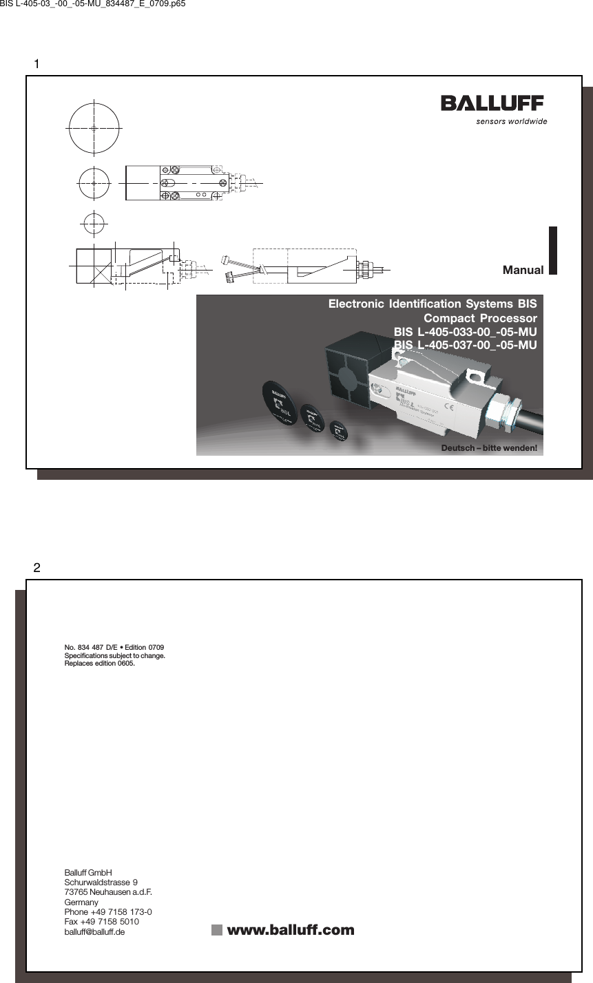
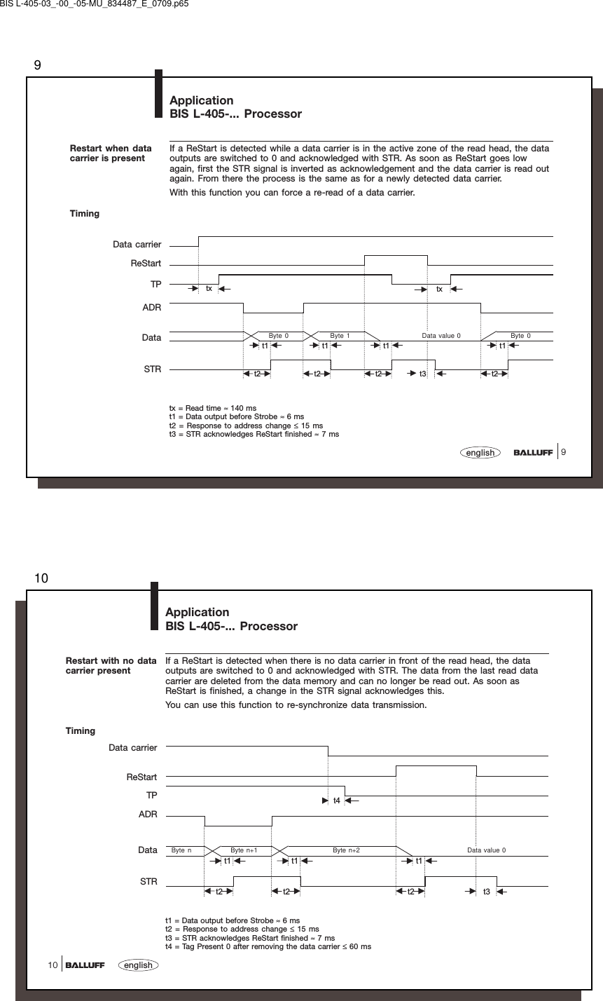
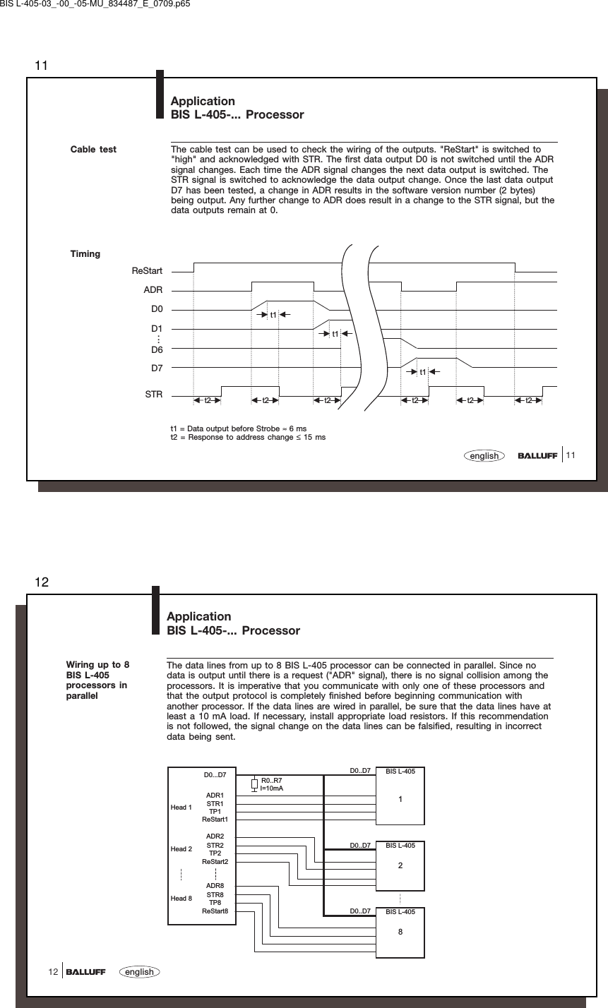
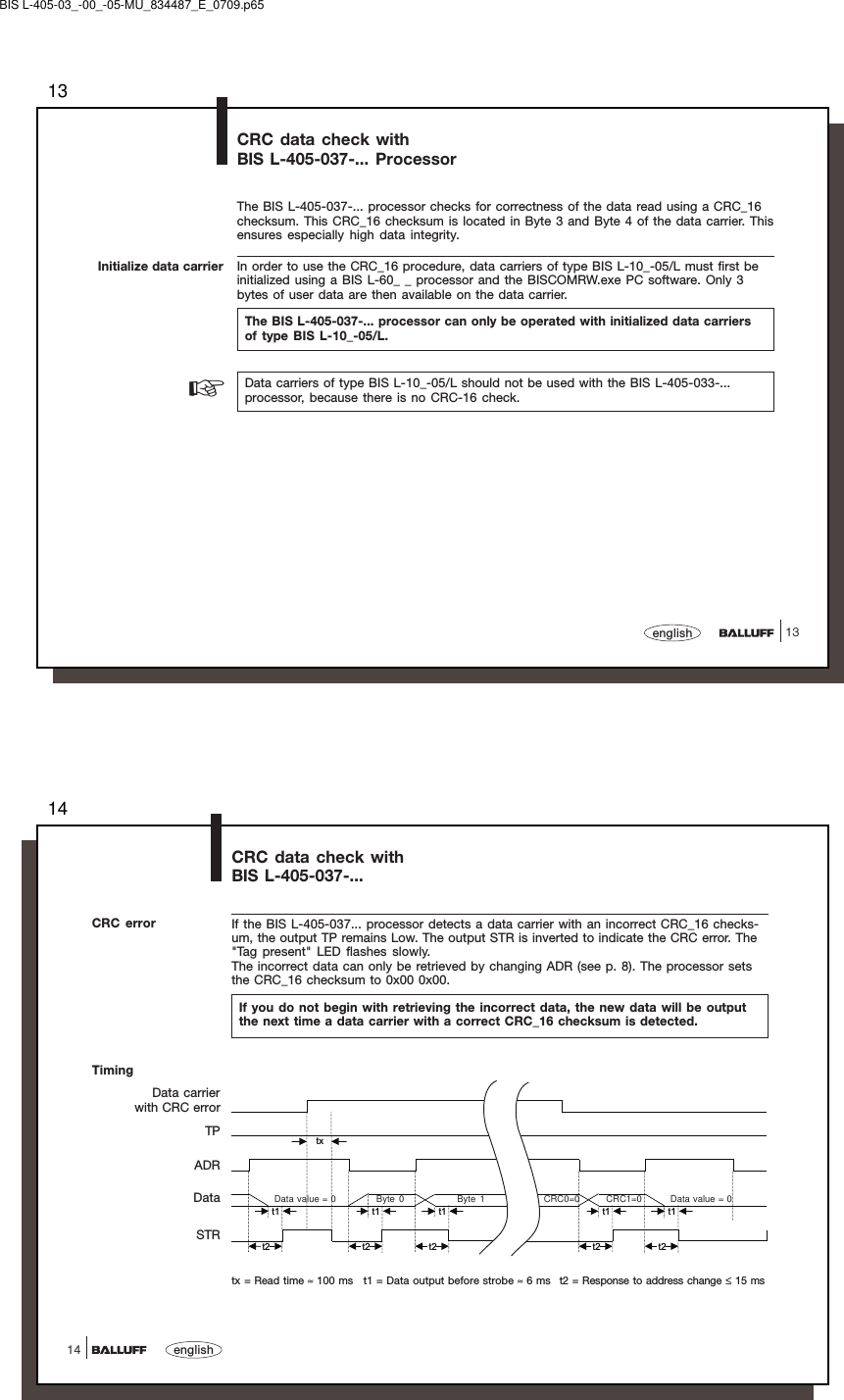
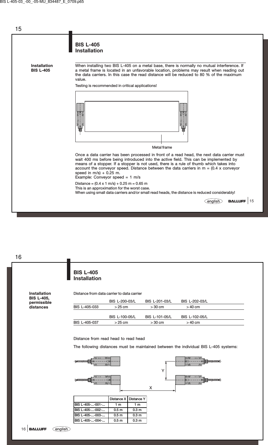
Balluff BISL405 BIS L-40X Series 3 User Manual BIS L 405 03 00 05 MU 834487 E 0709 p65

Balluff Inc BIS L-40X Series 3 BIS L 405 03 00 05 MU 834487 E 0709 p65

Contents

User Manual 1 of 2.pdf

1Electronic Identification Systems BISCompact ProcessorBIS L-405-033-00_-05-MUBIS L-405-037-00_-05-MUManualDeutsch – bitte wenden!BIS L-405-03_-00_-05-MU_834487_E_0709.p652No. 834 487 D/E • Edition 0709Specifications subject to change.Replaces edition 0605.Balluff GmbHSchurwaldstrasse 973765 Neuhausen a.d.F.GermanyPhone +49 7158 173-0Fax +49 7158 5010balluff@balluff.de www.balluff.com
33englishContentsSafety Notes ............................................................................................................................... 4Introduction BIS L-405 Identification System ........................................................................ 5/6Application BIS L-405 Processor .........................................................................................7-12CRC data check with BIS L-405-037-... Processor .......................................................... 13/14Installation L-405 ................................................................................................................. 15/16Installation L-405-...-001-........................................................................................................ 17Installation L-405-...-002-........................................................................................................ 18Installation L-405-...-003-........................................................................................................ 19Installation L-405-...-004-........................................................................................................ 20Installation ........................................................................................................................... 21/22Reorienting and Rotating the Read Head ............................................................................... 23Connection Diagrams ............................................................................................................... 24Technical  Data .......................................................................................................................... 25Ordering Information ................................................................................................................ 26Appendix, ASCII Table ............................................................................................................. 27BIS L-405-03_-00_-05-MU_834487_E_0709.p654english4Safety NotesBIS L-4_ _ processor together with the other BIS L system components comprise the Iden-tification System and may only be used for this purpose in industrial applications corre-sponding to Class A of the EMC Directive.Installation and operation are permitted by trained specialists only. Unauthorized modifica-tions and improper use will result in loss of the right to make warranty and liability claims.When installing the processor, follow exactly the connection diagrams provided later in thisdocument. Take special care when connecting the processor to external controllers, espe-cially with respect to the selection and polarity of the connections including the powersupply.Only approved power supplies may be used. For specific information, see the TechnicalData section.When deploying the identification system, all relevant safety regulations must be followed.In particular, measures must be taken to ensure that any defect in the identification systemdoes not result in a hazard to persons or equipment.This includes maintaining the permissible ambient conditions and regular inspection forproper function of the identification system and all the associated components.At the first sign that the identification system is not working properly, it should be takenout of service and guarded against unauthorized use.This document applies to the processor BIS L-405-03_-00_-05-MU (Software version V1.2and higher).ScopeMalfunctionInstallation andoperationDeployment andinspectionProper use andoperation
55englishPrincipleThis manual is intended to guide the user in installing and commissioning the componentsin the BIS L-405 identification system, so that start-up time is reduced to an absoluteminimum.The BIS L-405 identification system belongs to the category ofread-only, non-contacting systems.This function enables applications in which information which has been pre-coded into thedata carriers can be read out and used for further processing.The main areas of application include– in production for controlling material flow(e.g., for part-specific processes),in workpiece transport using conveying systems,for obtaining safety-relevant data,– in process materials organization.The processor and the read head form a compact unit which is contained in a plastichousing.The data carrier represents an independent unit. It does not require line-fed power andreceives its energy from the integrated read head in the BIS L-405 identification system.The read head continuously sends a carrier signal which supplies the data carrier as soonas the latter has reached the required distance from the read head. The read processtakes place during this phase. The data are output in 8-bit blocks over 8 parallel data linesand made available to the host system. These host systems may be:– a control computer (e.g., industrial PC) having a parallel port, or– a programmable logic controller (PLC).IntroductionBIS L-405 Identification SystemApplicationsSystem componentfunctionBIS L-405-03_-00_-05-MU_834487_E_0709.p656english6SystemcomponentsThe main components of the BIS L-405 identification system are–the processor with integrated read head, and–the data carrier(s).IntroductionBIS L-405 Identification SystemData carriers BIS L-2..Schematicrepresentation of anidentification system(example)Power TPPower TPConnections tohost system
77englishApplicationBIS L-405-... ProcessorSignal description Tag Present (TP): Indicates a data carrier in the field.Address (ADR): Signal change outputs the next data carrier address.Strobe (STR): This signal acknowledges the data output on the parallel interface.ReStart: Deletes the data memory in the BIS L-405 and sets all data outputs to0. The data carrier is then read again or, if no data carrier is present,only the data outputs are set to 0. This signal is also used to turn offthe read antenna. If two read heads are installed close together andinterfere with each other, this can deactivate one read head as long asthe other needs to be available.D0..D7: Data outputsWhen supply voltage is applied, the data outputs are in an undefined state for approx.100 ms. Then they switch to 0. The first byte cannot be read until the ADR signal changes.BIS L-405-03_-00_-05-MU_834487_E_0709.p658english8ApplicationBIS L-405-... ProcessorTimingRead 5 bytes Detection of a new data carrier is indicated by the TP signal. The first data value is notoutput until the ADR input signal changes. Each time ADR changes, the value of the nextaddress is given to the data outputs. As an acknowledgement of the data change, theprocessor invertes the STR signal. Once the last byte is output, a change in ADR isfollowed by a data value output of 0. Any further change to ADR does result in a change tothe STR signal, but the data remain 0. This is how the end of data can be recognized.If the data carrier leaves the read head before all the data have been output, the dataremain stored for a subsequent data read. Before a new data carrier is recognized by theread head, data transmission must have been completed.If the next data carrier enters the read zone before the data have been picked up, the "TagPresent" (Overflow) LED will indicate this by flashing. The data from the new tag are notoutput, and a ReStart must be performed to resynchronize.tx txt1 t1 t1 t1 t1t2 t2 t2 t2 t2 t2Data value = 0 Byte 0 Byte 1 Byte 3 Byte 4 Data value = 0Data carrierTPADRDataSTRtx = Read time ≈ 140 ms t1 = Data output before Strobe ≈ 6 ms t2 = Response to address change ≤ 15 ms
99englishApplicationBIS L-405-... ProcessorRestart when datacarrier is presentIf a ReStart is detected while a data carrier is in the active zone of the read head, the dataoutputs are switched to 0 and acknowledged with STR. As soon as ReStart goes lowagain, first the STR signal is inverted as acknowledgement and the data carrier is read outagain. From there the process is the same as for a newly detected data carrier.With this function you can force a re-read of a data carrier.TimingData carrierReStartTPADRDataSTRtxt1 t1 t1 t1t3t2 t2txt2 t2Byte 0 Byte 1 Data value 0 Byte 0tx = Read time ≈ 140 mst1 = Data output before Strobe ≈ 6 mst2 = Response to address change ≤ 15 mst3 = STR acknowledges ReStart finished ≈ 7 msBIS L-405-03_-00_-05-MU_834487_E_0709.p6510english10ApplicationBIS L-405-... ProcessorRestart with no datacarrier presentIf a ReStart is detected when there is no data carrier in front of the read head, the dataoutputs are switched to 0 and acknowledged with STR. The data from the last read datacarrier are deleted from the data memory and can no longer be read out. As soon asReStart is finished, a change in the STR signal acknowledges this.You can use this function to re-synchronize data transmission.Timingt4t1 t1 t1t3t2 t2 t2Byte n Byte n+1 Byte n+2 Data value 0Data carrierReStartTPADRDataSTRt1 = Data output before Strobe ≈ 6 mst2 = Response to address change ≤ 15 mst3 = STR acknowledges ReStart finished ≈ 7 mst4 = Tag Present 0 after removing the data carrier ≤ 60 ms
1111englishApplicationBIS L-405-... ProcessorCable test The cable test can be used to check the wiring of the outputs. "ReStart" is switched to"high" and acknowledged with STR. The first data output D0 is not switched until the ADRsignal changes. Each time the ADR signal changes the next data output is switched. TheSTR signal is switched to acknowledge the data output change. Once the last data outputD7 has been tested, a change in ADR results in the software version number (2 bytes)being output. Any further change to ADR does result in a change to the STR signal, but thedata outputs remain at 0.TimingReStartADRD0D1D6D7STRt1t1t1t2 t2 t2 t2 t2 t2t1 = Data output before Strobe ≈ 6 mst2 = Response to address change ≤ 15 ms...BIS L-405-03_-00_-05-MU_834487_E_0709.p6512english12ApplicationBIS L-405-... ProcessorWiring up to 8BIS L-405processors inparallelThe data lines from up to 8 BIS L-405 processor can be connected in parallel. Since nodata is output until there is a request ("ADR" signal), there is no signal collision among theprocessors. It is imperative that you communicate with only one of these processors andthat the output protocol is completely finished before beginning communication withanother processor. If the data lines are wired in parallel, be sure that the data lines have atleast a 10 mA load. If necessary, install appropriate load resistors. If this recommendationis not followed, the signal change on the data lines can be falsified, resulting in incorrectdata being sent.D0..D7ADR1STR1TP1ReStart1ADR2STR2 D0..D7TP2ReStart2ADR8STR8TP8ReStart8 D0..D7D0...D7 R0..R7I=10mAHead 1Head 282BIS L-405BIS L-405BIS L-4051Head 8
1313englishCRC data check withBIS L-405-037-... ProcessorInitialize data carrierThe BIS L-405-037-... processor checks for correctness of the data read using a CRC_16checksum. This CRC_16 checksum is located in Byte 3 and Byte 4 of the data carrier. Thisensures especially high data integrity.In order to use the CRC_16 procedure, data carriers of type BIS L-10_-05/L must first beinitialized using a BIS L-60_ _ processor and the BISCOMRW.exe PC software. Only 3bytes of user data are then available on the data carrier.The BIS L-405-037-... processor can only be operated with initialized data carriersof type BIS L-10_-05/L.☞Data carriers of type BIS L-10_-05/L should not be used with the BIS L-405-033-...processor, because there is no CRC-16 check.BIS L-405-03_-00_-05-MU_834487_E_0709.p6514english14txt1 t1 t1 t1 t1t2 t2 t2 t2 t2CRC data check withBIS L-405-037-...CRC error If the BIS L-405-037... processor detects a data carrier with an incorrect CRC_16 checks-um, the output TP remains Low. The output STR is inverted to indicate the CRC error. The"Tag present" LED flashes slowly.The incorrect data can only be retrieved by changing ADR (see p. 8). The processor setsthe CRC_16 checksum to 0x00 0x00.If you do not begin with retrieving the incorrect data, the new data will be outputthe next time a data carrier with a correct CRC_16 checksum is detected.TimingData carrierwith CRC errorTPADRDataSTRtx = Read time ≈ 100 ms t1 = Data output before strobe ≈ 6 ms t2 = Response to address change ≤ 15 msData value = 0 Byte 0 Byte 1 CRC0=0 CRC1=0 Data value = 0
1515englishPower TPPower TPBIS L-405InstallationMetal frameInstallationBIS L-405When installing two BIS L-405 on a metal base, there is normally no mutual interference. Ifa metal frame is located in an unfavorable location, problems may result when reading outthe data carriers. In this case the read distance will be reduced to 80 % of the maximumvalue.Testing is recommended in critical applications!Once a data carrier has been processed in front of a read head, the next data carrier mustwait 400 ms before being introduced into the active field. This can be implemented bymeans of a stopper. If a stopper is not used, there is a rule of thumb which takes intoaccount the conveyor speed. Distance between the data carriers in m = (0.4 x conveyorspeed in m/s) + 0.25 m.Example: Conveyor speed = 1 m/sDistance = (0.4 x 1 m/s) + 0.25 m = 0.65 mThis is an approximation for the worst case.When using small data carriers and/or small read heads, the distance is reduced considerably!BIS L-405-03_-00_-05-MU_834487_E_0709.p6516english16BIS L-405InstallationInstallationBIS L-405,permissibledistancesDistance from data carrier to data carrierBIS L-200-03/L BIS L-201-03/L BIS L-202-03/LBIS  L-405-033       > 25 cm       > 30 cm       > 40 cmBIS L-100-05/L BIS L-101-05/L BIS L-102-05/LBIS  L-405-037       > 25 cm       > 30 cm       > 40 cmDistance from read head to read headThe following distances must be maintained between the individual BIS L-405 systems:XYDistance X Distance YBIS L-405-...-001-... 1 m 1 mBIS L-405-...-002-... 0.5 m 0.3 mBIS L-405-...-003-... 0.5 m 0.3 mBIS L-405-...-004-... 0.5 m 0.3 m
1717englishSpecifications bydata carrierBIS L-405-037-001-...BIS L-405-...-001-...InstallationSpecifications bydata carrierBIS L-405-033-001-...Speeds:Clear zone anddistancesSpecificatio ns bydata carrier(installed in clearzone)For v = 0 (static condition)Readdistance (mm) Offset to center axis atdistance of: (mm)0-25 0-35 0-45 0-15BIS  L-200-03 0 - 30 ± 15 -BIS  L-201-03 0 - 40 - ± 20 - -BIS  L-202-03 0 - 55 - - ± 30 -BIS  L-203-03 0 - 20 - - - ± 10307.3ø5.340ø1007.35.3 (3x)60461206.540Power T PClear zoneSet screwActive surfaceLSpecificatio nsused with datacarrier (installed inclear zone)For v = 0 (static mode)Readdistance (mm) Offset to center axis atdistance of: (mm)0-25 0-35 0-45 0-15BIS  L-100-05 0 - 30 ± 15 -BIS  L-101-05 0 - 40 - ± 20 - -BIS  L-102-05 0 - 55 - - ± 30 -BIS  L-103-05 0 - 20 - - - ± 10At readdistance[mm]Speed [m/s]BIS L-200-03 15 0.4BIS L-201-03 20 0.45BIS  L-202-03 27.5 0.5BIS L-203-03 10 0.28At readdistance[mm]Speed [m/s]BIS L-100-05 15 0.45BIS L-101-05 20 0.5BIS L-102-05 27.5 0.72BIS L-103-05 10 0.36BIS L-405-03_-00_-05-MU_834487_E_0709.p6518english18BIS L-405-...-002-...InstallationInstallationBIS L-405-...-002-...Specifications bydata carrierBIS L-405-037-002-...Specifications bydata carrierBIS L-405-033-002-...Specificatio ns bydata carrier(installed in clearzone)For v = 0 (static condition)Readdistance (mm) Offset to center axis atdistance of: (mm)0-10 0-15 0-20 0-25BIS  L-200-03 0 -23 ± 12 ± 12 ± 8 -BIS  L-201-03 0 - 27 ± 15 ± 15 ± 15 ± 6BIS L-203-03 0 - 16 ± 8 ± 4 - -Speeds:Specificatio ns bydata carrier(installed in clearzone)For v = 0 (static condition)Readdistance (mm) Offset to center axis atdistance of: (mm)0-10 0-15 0-20 0-25BIS  L-100-05 0 -23 ± 12 ± 12 ± 8 -BIS  L-101-05 0 - 27 ± 15 ± 15 ± 15 ± 6BIS L-103-05 0 - 16 ± 8 ± 4 - -Set screwCable length50 cmActive surfaceStandard length 5 mClear zoneAt readdistance[mm]Speed [m/s]BIS  L-200-03 11.5 0.18BIS  L-201-03 13.5 0.22BIS L-203-03 8 0.15At readdistance[mm]Speed [m/s]BIS  L-100-05 11.5 0.22BIS  L-101-05 13.5 0.3BIS L-103-05 8 0.18
1919englishBIS L-405-...-003-...InstallationInstallationBIS L-405-...-003-...Specifications bydata carrierBIS L-405-037-003-...Specificatio ns bydata carrier(installed i n clearzone)For v = 0 (static condition)Readdistance (mm) Offset to centeraxis at distance of:(mm)0-5 0-8 0-11BIS L-103-05 0 - 11 ± 6 ± 4 ± 2Specifications bydata carrierBIS L-405-033-003-...Specificatio ns bydata carrier(installed i n clearzone)For v = 0 (static condition)Readdistance (mm) Offset to centeraxis at distance of:(mm)0-5 0-8 0-11BIS L-203-03 0 - 11 ± 6 ± 4 ± 2Speeds:Standard length 5 m(max. 20 m)At readdistance[mm]Speed [m/s]BIS L-203-03 51.5 0.11At readdistance[mm]Speed [m/s]BIS L-103-05 5.5 0.14BIS L-405-03_-00_-05-MU_834487_E_0709.p6520english20InstallationBIS L-405-...-004-...Specifications bydata carrierBIS L-405-037-004-...Specifications bydata carrierBIS L-405-033-004-...BIS L-405-...-004-...InstallationSpecificatio ns bydata carrier(installed in clearzone)For v = 0 (static condition)Readdistance (mm) Offset to center axis atdistance of: (mm)0-10 0-15 0-20 0-25BIS  L-100-05 0 -23 ± 12 ± 12 ± 8 -BIS  L-101-05 0 - 27 ± 15 ± 15 ± 15 ± 6BIS L-103-05 0 - 16 ± 8 ± 4 - -Specificatio ns bydata carrier(installed in clearzone)For v = 0 (static condition)Readdistance (mm) Offset to center axis atdistance of: (mm)0-10 0-15 0-20 0-25BIS  L-200-03 0 -23 ± 12 ± 12 ± 8 -BIS  L-201-03 0 - 27 ± 15 ± 15 ± 15 ± 6BIS L-203-03 0 - 16 ± 8 ± 4 - -Speeds:At readdistance[mm]Speed [m/s]BIS L-200-03 11.5 0.18BIS L-201-03 13.5 0.22BIS L-203-03 8 0.15At readdistance[mm]Speed [m/s]BIS  L-100-05 11.5 0.22BIS  L-101-05 13.5 0.3BIS L-103-05 8 0.18Set screwActive surfaceCable length 50 cmStandard length 5 m(max. 20 m)Clear zone 50Clear zone 50Clear zone 50
2121englishBIS L-405InstallationLead assignmentsBIS L-503-... Connection for Description ColorSUPPLY VOLTAGE +24 V DC RED0 V DC BLUEOUTPUTSBit 0 WHITEBit 1 BROWNBit 2 GREENBit 3 YELLOWBit 4 GRAYBit 5 ROSEBit 6 BLACKBit 7 VIOLETTP WHITE/GREENSTR BROWN/GREENINPUTS0V WHITE/YELLOWReStart GRAY/ROSEADR RED/BLUESHIELDING SHIELD -n/c - YELLOW/BROWNBIS L-405-03_-00_-05-MU_834487_E_0709.p6522english22BIS L-405InstallationWhen installing BIS L-405 and BIS L-503, remove the PG fitting. Insert BIS L-503 plug intothe correct sockets of the BIS L-405. Tighten screws and PG fitting.  Remove PG fitting before opening BIS L-405 and BIS L-503.Installing theBIS L-405 Processor☞Active surface Set screw BIS L405 moduleBIS L-503 mounting basePower TPSet screw Screws for fasteningmounting base
2323englishBIS L-405Reorienting and Rotating the Read HeadReorienting the readhead- Remove the two screws on the read head base- Turn the read head module 180°- Tighten both screws- Unscrew the set screw- Read head module can be rotated stepless (complete with read head base) to the  desired position (range: 270°)- Tighten set screw- Read head module is secured against over-rotationRotating the readhead  Read head modules are not interchangeable!Active surfacepositions☞Read headbaseScrewActivesurfaceSet screw BIS L405 moduleBIS L-503mounting baseRead headmoduleBIS L-405-03_-00_-05-MU_834487_E_0709.p6524english24BIS L-405Connection DiagramsWiring the inputsWiring the outputsfor dataDC+24 V–ADR, ReStartDC+24 V–D0...D 7, STR, TPLoadOpto-couplerSupply voltage: DC 24 V +10% / –20% (incl. ripple)Input high: min. 17 V, typ. 3 mAInput low: max. 6 V, < 1.5 mASupply voltage: DC 24 V +10% / –20% (incl. ripple)Output current: max. 50 mAVoltage drop at 50 mA: < 1.5 V
2525englishGeneral data Housing Plastic (PBT)Ambient temperature 0 °C to +60 °CEnclosure rating IP 67 (only when assembled)Supply voltage DC 24 V +10 % / –20 % (incl. ripple)Current consumption ≤ 50 mA with no loadOutput current per output max. 50 mAPower LED greenTag Present LED yellowOverflow LED yellow flashing(The "Tag Present" LED flashes rapidly if the datafrom a data carrier were not completely read and anew data carrier has arrived in the active zone.)BIS L-405Technical DataTemperature rangeEnclosure ratingSupply voltageThe CE Marking verifies that our products conform to the requirements of theEU Directive2004/108/EC (EMC Directive)and the EMC Law. In our EMC Laboratory, which is accredited by the DATech for TestingElectromagnetic Compatibility, we have verified that Balluff products meet the EMC re-quirements of the following Generic Standards:EN 61000-6-4  (Emission), EN 61000-6-2  (Noise Immunity).LED functionindicatorBIS L-405-03_-00_-05-MU_834487_E_0709.p6526english26Balluff Identification SystemSeries LHardware-Type405 = Plastic housingSoftware-Type033 = 8 bits parallel037 = 8 bits parallel with CRC_16 data checkHardware version001 = Coil Ø 34 mm002 = discharged read head modules M18 (0.5 m cable)003 = discharged read head modules M12 (0.5 m cable)004 = discharged read head modules C-305 housing (0.5 m cable)Interface05 = parallelModuleMU = Module unitUsed only together with mounting base BIS L-503-PU1-...BIS L-405-03_-00_-05-MUBIS L-405Ordering InformationPart Numbers  Read head modules are not interchangeable!☞
2727englishAppendix, ASCII TableDeci-mal Hex ControlCode ASCII Deci-mal Hex ControlCode ASCII Deci-mal Hex ASCII Deci-mal Hex ASCII Deci-mal Hex ASCII Deci-mal Hex ASCII0 00 Ctrl @ NUL 22 16 Ctrl V SYN 44 2C , 65 41 A 86 56 V 107 6B k1 01 Ctrl A SOH 23 17 Ctrl W ETB 45 2D - 66 42 B 87 57 W 108 6C l2 02 Ctrl B STX 24 18 Ctrl X CAN 46 2E . 67 43 C 88 58 X 109 6D m3 03 Ctrl C ETX 25 19 Ctrl Y EM 47 2F / 68 44 D 89 59 Y 110 6E n4 04 Ctrl D EOT 26 1A Ctrl Z SUB 48 30 0 69 45 E 90 5A Z 111 6F o5 05 Ctrl E ENQ 27 1B Ctrl [ ESC 49 31 1 70 46 F 91 5B [ 112 70 p6 06 Ctrl F ACK 28 1C Ctrl \ FS 50 32 2 71 47 G 92 5C \ 113 71 q7 07 Ctrl G BEL 29 1D Ctrl ] GS 51 33 3 72 48 H 93 5D ] 114 72 r8 08 Ctrl H BS 30 1E Ctrl ^ RS 52 34 4 73 49 I 94 5E ^ 115 73 s9 09 Ctrl I HT 31 1F Ctrl _ US 53 35 5 74 4A J 95 5F _ 116 74 t10 0A Ctrl J LF 32 20 SP 54 36 6 75 4B K 96 60 ` 117 75 u11 0B Ctrl K VT 33 21 ! 55 37 7 76 4C L 97 61 a 118 76 v12 0C Ctrl L FF 34 22 " 56 38 8 77 4D M 98 62 b 119 77 w13 0D Ctrl M CR 35 23 # 57 39 9 78 4E N 99 63 c 120 78 x14 0E Ctrl N SO 36 24 $ 58 3A : 79 4F O 100 64 d 121 79 y15 0F Ctrl O SI 37 25 % 59 3B ; 80 50 P 101 65 e 122 7A z16 10 Ctrl P DLE 38 26 & 60 3C < 81 51 Q 102 66 f 123 7B {17 11 Ctrl Q DC1 39 27 ' 61 3D = 82 52 R 103 67 g 124 7C |18 12 Ctrl R DC2 40 28 ( 62 3E > 83 53 S 104 68 h 125 7D }19 13 Ctrl S DC3 41 29 ) 63 3F ? 84 54 T 105 69 i 126 7E ~20 14 Ctrl T DC4 42 2A * 64 40 @ 85 55 U 106 6A j 127 7F DEL21 15 Ctrl U NAK 43 2B +BIS L-405-03_-00_-05-MU_834487_E_0709.p65

Navigation menu