Balluff BISL405 BIS L-40X Series 3 User Manual BIS L 405 03 00 05 MU 834487 E 0709 p65
Balluff Inc BIS L-40X Series 3 BIS L 405 03 00 05 MU 834487 E 0709 p65
Balluff >
Contents
- 1. User Manual 1 of 2.pdf
- 2. User Manual 2 of 2.pdf
User Manual 1 of 2.pdf
1
Electronic Identification Systems BIS
Compact Processor
BIS L-405-033-00_-05-MU
BIS L-405-037-00_-05-MU
Manual
Deutsch – bitte wenden!
BIS L-405-03_-00_-05-MU_834487_E_0709.p65
2
No. 834 487 D/E • Edition 0709
Specifications subject to change.
Replaces edition 0605.
Balluff GmbH
Schurwaldstrasse 9
73765 Neuhausen a.d.F.
Germany
Phone +49 7158 173-0
Fax +49 7158 5010
balluff@balluff.de www.balluff.com
3
3
english
Contents
Safety Notes ............................................................................................................................... 4
Introduction BIS L-405 Identification System ........................................................................ 5/6
Application BIS L-405 Processor .........................................................................................7-12
CRC data check with BIS L-405-037-... Processor .......................................................... 13/14
Installation L-405 ................................................................................................................. 15/16
Installation L-405-...-001-........................................................................................................ 17
Installation L-405-...-002-........................................................................................................ 18
Installation L-405-...-003-........................................................................................................ 19
Installation L-405-...-004-........................................................................................................ 20
Installation ........................................................................................................................... 21/22
Reorienting and Rotating the Read Head ............................................................................... 23
Connection Diagrams ............................................................................................................... 24
Technical Data .......................................................................................................................... 25
Ordering Information ................................................................................................................ 26
Appendix, ASCII Table ............................................................................................................. 27
BIS L-405-03_-00_-05-MU_834487_E_0709.p65
4
english4
Safety Notes
BIS L-4_ _ processor together with the other BIS L system components comprise the Iden-
tification System and may only be used for this purpose in industrial applications corre-
sponding to Class A of the EMC Directive.
Installation and operation are permitted by trained specialists only. Unauthorized modifica-
tions and improper use will result in loss of the right to make warranty and liability claims.
When installing the processor, follow exactly the connection diagrams provided later in this
document. Take special care when connecting the processor to external controllers, espe-
cially with respect to the selection and polarity of the connections including the power
supply.
Only approved power supplies may be used. For specific information, see the Technical
Data section.
When deploying the identification system, all relevant safety regulations must be followed.
In particular, measures must be taken to ensure that any defect in the identification system
does not result in a hazard to persons or equipment.
This includes maintaining the permissible ambient conditions and regular inspection for
proper function of the identification system and all the associated components.
At the first sign that the identification system is not working properly, it should be taken
out of service and guarded against unauthorized use.
This document applies to the processor BIS L-405-03_-00_-05-MU (Software version V1.2
and higher).
Scope
Malfunction
Installation and
operation
Deployment and
inspection
Proper use and
operation
5
5
english
Principle
This manual is intended to guide the user in installing and commissioning the components
in the BIS L-405 identification system, so that start-up time is reduced to an absolute
minimum.
The BIS L-405 identification system belongs to the category of
read-only, non-contacting systems.
This function enables applications in which information which has been pre-coded into the
data carriers can be read out and used for further processing.
The main areas of application include
– in production for controlling material flow
(e.g., for part-specific processes),
in workpiece transport using conveying systems,
for obtaining safety-relevant data,
– in process materials organization.
The processor and the read head form a compact unit which is contained in a plastic
housing.
The data carrier represents an independent unit. It does not require line-fed power and
receives its energy from the integrated read head in the BIS L-405 identification system.
The read head continuously sends a carrier signal which supplies the data carrier as soon
as the latter has reached the required distance from the read head. The read process
takes place during this phase. The data are output in 8-bit blocks over 8 parallel data lines
and made available to the host system. These host systems may be:
– a control computer (e.g., industrial PC) having a parallel port, or
– a programmable logic controller (PLC).
Introduction
BIS L-405 Identification System
Applications
System component
function
BIS L-405-03_-00_-05-MU_834487_E_0709.p65
6
english6
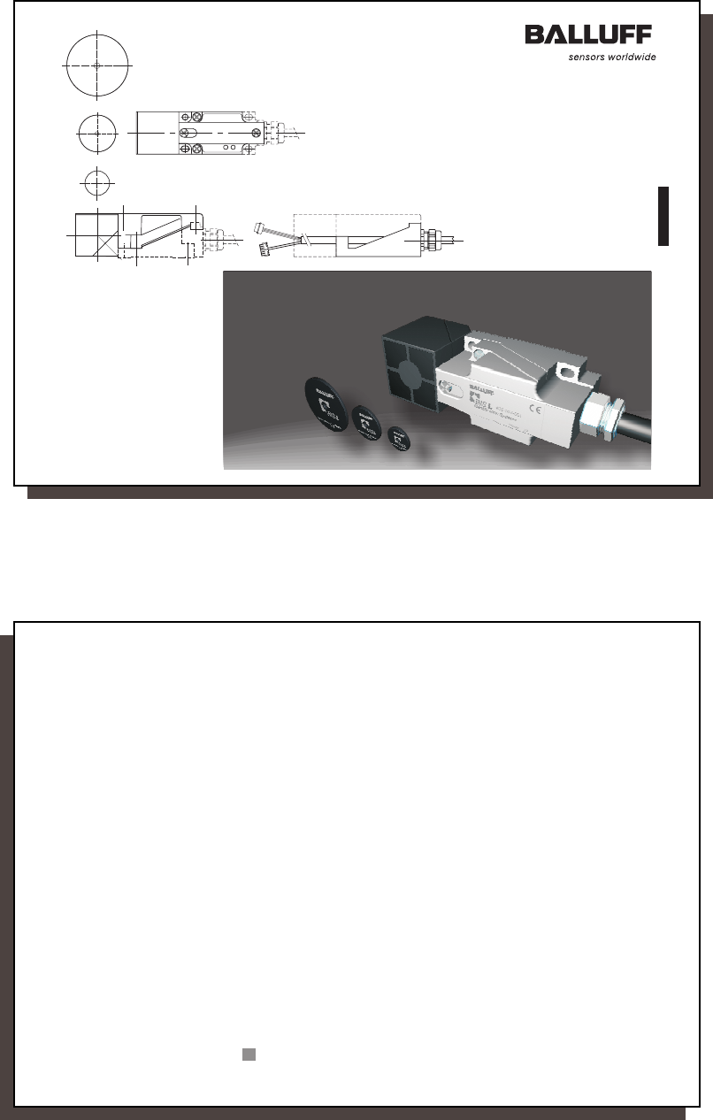
System
components
The main components of the BIS L-405 identification system are
–the processor with integrated read head, and
–the data carrier(s).
Introduction
BIS L-405 Identification System
Data carriers BIS L-2..
Schematic
representation of an
identification system
(example)
Power TP
Power TP
Connections to
host system
7
7
english
Application
BIS L-405-... Processor
Signal description Tag Present (TP): Indicates a data carrier in the field.
Address (ADR): Signal change outputs the next data carrier address.
Strobe (STR): This signal acknowledges the data output on the parallel interface.
ReStart: Deletes the data memory in the BIS L-405 and sets all data outputs to
0. The data carrier is then read again or, if no data carrier is present,
only the data outputs are set to 0. This signal is also used to turn off
the read antenna. If two read heads are installed close together and
interfere with each other, this can deactivate one read head as long as
the other needs to be available.
D0..D7: Data outputs
When supply voltage is applied, the data outputs are in an undefined state for approx.
100 ms. Then they switch to 0. The first byte cannot be read until the ADR signal changes.
BIS L-405-03_-00_-05-MU_834487_E_0709.p65
8
english8
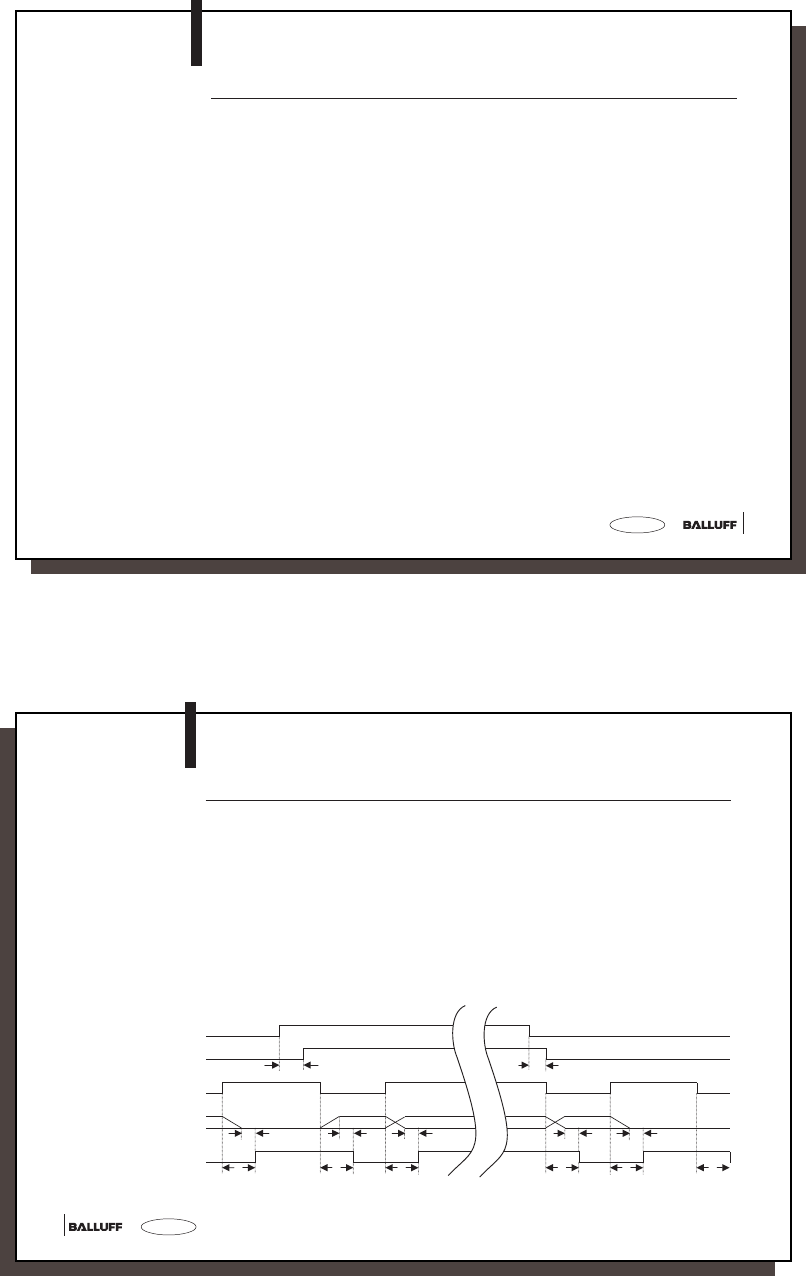
Application
BIS L-405-... Processor
Timing
Read 5 bytes Detection of a new data carrier is indicated by the TP signal. The first data value is not
output until the ADR input signal changes. Each time ADR changes, the value of the next
address is given to the data outputs. As an acknowledgement of the data change, the
processor invertes the STR signal. Once the last byte is output, a change in ADR is
followed by a data value output of 0. Any further change to ADR does result in a change to
the STR signal, but the data remain 0. This is how the end of data can be recognized.
If the data carrier leaves the read head before all the data have been output, the data
remain stored for a subsequent data read. Before a new data carrier is recognized by the
read head, data transmission must have been completed.
If the next data carrier enters the read zone before the data have been picked up, the "Tag
Present" (Overflow) LED will indicate this by flashing. The data from the new tag are not
output, and a ReStart must be performed to resynchronize.
tx tx
t1 t1 t1 t1 t1
t2 t2 t2 t2 t2 t2
Data value = 0 Byte 0 Byte 1 Byte 3 Byte 4 Data value = 0
Data carrier
TP
ADR
Data
STR
tx = Read time ≈ 140 ms t1 = Data output before Strobe ≈ 6 ms t2 = Response to address change ≤ 15 ms
9
9
english
Application
BIS L-405-... Processor
Restart when data
carrier is present
If a ReStart is detected while a data carrier is in the active zone of the read head, the data
outputs are switched to 0 and acknowledged with STR. As soon as ReStart goes low
again, first the STR signal is inverted as acknowledgement and the data carrier is read out
again. From there the process is the same as for a newly detected data carrier.
With this function you can force a re-read of a data carrier.
Timing
Data carrier
ReStart
TP
ADR
Data
STR
tx
t1 t1 t1 t1
t3
t2 t2
tx
t2 t2
Byte 0 Byte 1 Data value 0 Byte 0
tx = Read time ≈ 140 ms
t1 = Data output before Strobe ≈ 6 ms
t2 = Response to address change ≤ 15 ms
t3 = STR acknowledges ReStart finished ≈ 7 ms
BIS L-405-03_-00_-05-MU_834487_E_0709.p65
10
english10
Application
BIS L-405-... Processor
Restart with no data
carrier present
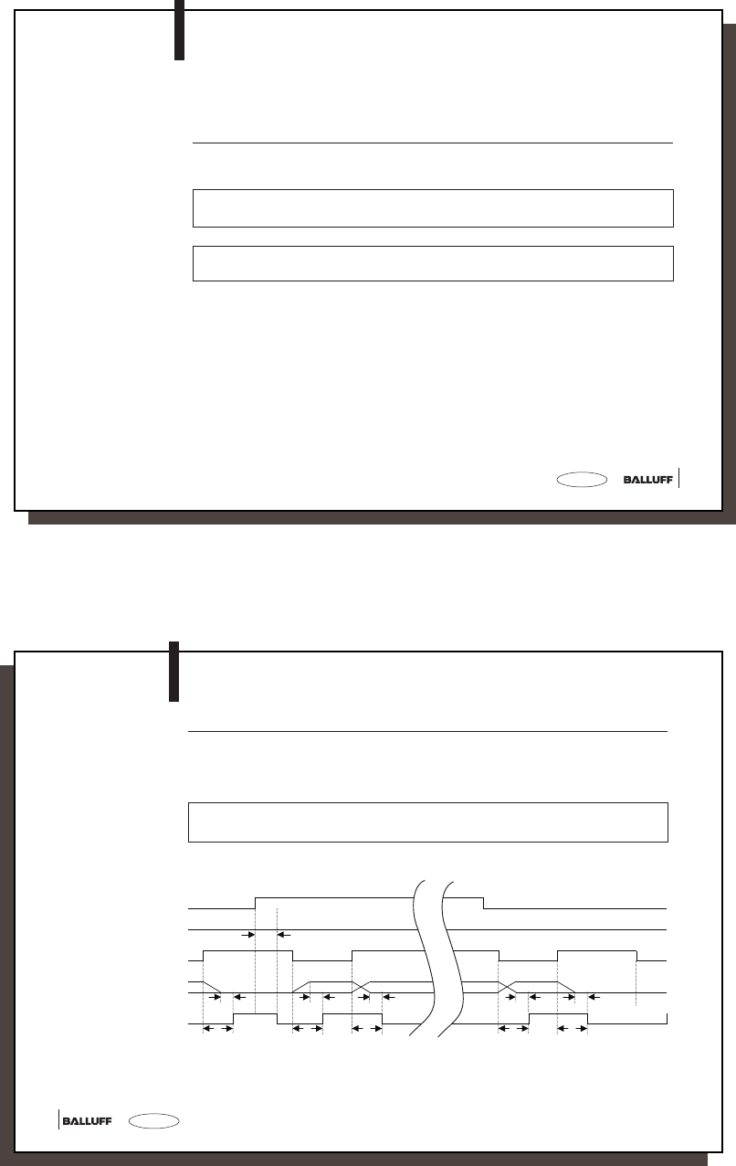
If a ReStart is detected when there is no data carrier in front of the read head, the data
outputs are switched to 0 and acknowledged with STR. The data from the last read data
carrier are deleted from the data memory and can no longer be read out. As soon as
ReStart is finished, a change in the STR signal acknowledges this.
You can use this function to re-synchronize data transmission.
Timing
t4
t1 t1 t1
t3t2 t2 t2
Byte n Byte n+1 Byte n+2 Data value 0
Data carrier
ReStart
TP
ADR
Data
STR
t1 = Data output before Strobe ≈ 6 ms
t2 = Response to address change ≤ 15 ms
t3 = STR acknowledges ReStart finished ≈ 7 ms
t4 = Tag Present 0 after removing the data carrier ≤ 60 ms
11
11
english
Application
BIS L-405-... Processor
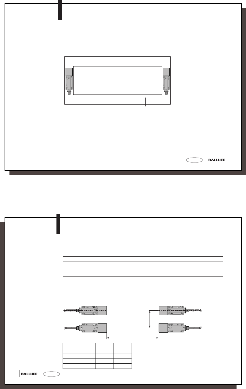
Cable test The cable test can be used to check the wiring of the outputs. "ReStart" is switched to
"high" and acknowledged with STR. The first data output D0 is not switched until the ADR
signal changes. Each time the ADR signal changes the next data output is switched. The
STR signal is switched to acknowledge the data output change. Once the last data output
D7 has been tested, a change in ADR results in the software version number (2 bytes)
being output. Any further change to ADR does result in a change to the STR signal, but the
data outputs remain at 0.
Timing
ReStart
ADR
D0
D1
D6
D7
STR
t1
t1
t1
t2 t2 t2 t2 t2 t2
t1 = Data output before Strobe ≈ 6 ms
t2 = Response to address change ≤ 15 ms
...
BIS L-405-03_-00_-05-MU_834487_E_0709.p65
12
english12
Application
BIS L-405-... Processor
Wiring up to 8
BIS L-405
processors in
parallel
The data lines from up to 8 BIS L-405 processor can be connected in parallel. Since no
data is output until there is a request ("ADR" signal), there is no signal collision among the
processors. It is imperative that you communicate with only one of these processors and
that the output protocol is completely finished before beginning communication with
another processor. If the data lines are wired in parallel, be sure that the data lines have at
least a 10 mA load. If necessary, install appropriate load resistors. If this recommendation
is not followed, the signal change on the data lines can be falsified, resulting in incorrect
data being sent.
D0..D7
ADR1
STR1
TP1
ReStart1
ADR2
STR2 D0..D7
TP2
ReStart2
ADR8
STR8
TP8
ReStart8 D0..D7
D0...D7 R0..R7
I=10mA
Head 1
Head 2
8
2
BIS L-405
BIS L-405
BIS L-405
1
Head 8
13
13
english
CRC data check with
BIS L-405-037-... Processor
Initialize data carrier
The BIS L-405-037-... processor checks for correctness of the data read using a CRC_16
checksum. This CRC_16 checksum is located in Byte 3 and Byte 4 of the data carrier. This
ensures especially high data integrity.
In order to use the CRC_16 procedure, data carriers of type BIS L-10_-05/L must first be
initialized using a BIS L-60_ _ processor and the BISCOMRW.exe PC software. Only 3
bytes of user data are then available on the data carrier.
The BIS L-405-037-... processor can only be operated with initialized data carriers
of type BIS L-10_-05/L.
☞Data carriers of type BIS L-10_-05/L should not be used with the BIS L-405-033-...
processor, because there is no CRC-16 check.
BIS L-405-03_-00_-05-MU_834487_E_0709.p65
14
english14
tx
t1 t1 t1 t1 t1
t2 t2 t2 t2 t2
CRC data check with
BIS L-405-037-...
CRC error If the BIS L-405-037... processor detects a data carrier with an incorrect CRC_16 checks-
um, the output TP remains Low. The output STR is inverted to indicate the CRC error. The
"Tag present" LED flashes slowly.
The incorrect data can only be retrieved by changing ADR (see p. 8). The processor sets
the CRC_16 checksum to 0x00 0x00.
If you do not begin with retrieving the incorrect data, the new data will be output
the next time a data carrier with a correct CRC_16 checksum is detected.
Timing
Data carrier
with CRC error
TP
ADR
Data
STR
tx = Read time ≈ 100 ms t1 = Data output before strobe ≈ 6 ms t2 = Response to address change ≤ 15 ms
Data value = 0 Byte 0 Byte 1 CRC0=0 CRC1=0 Data value = 0
15
15
english
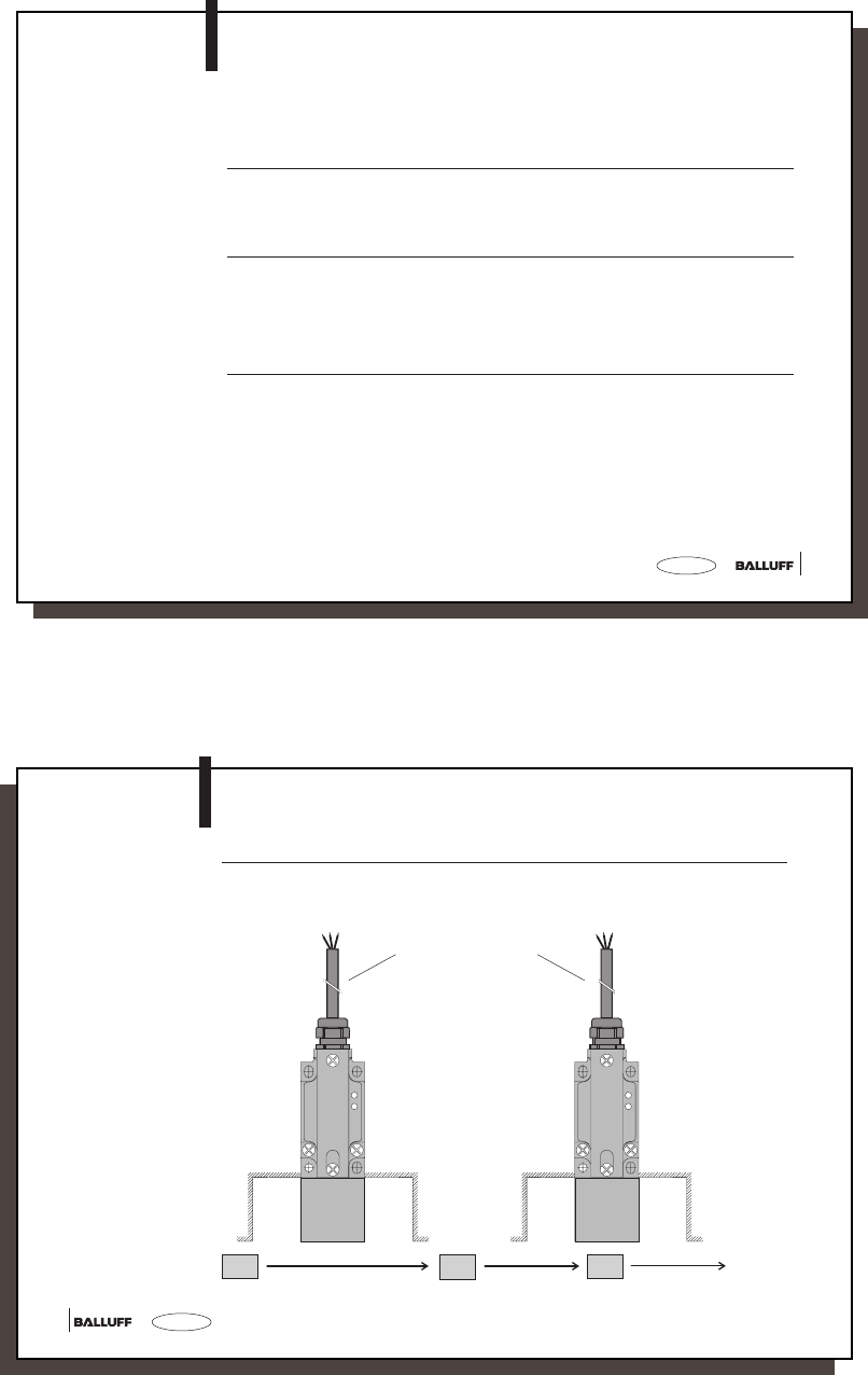
Power TP
Power TP
BIS L-405
Installation
Metal frame
Installation
BIS L-405
When installing two BIS L-405 on a metal base, there is normally no mutual interference. If
a metal frame is located in an unfavorable location, problems may result when reading out
the data carriers. In this case the read distance will be reduced to 80 % of the maximum
value.
Testing is recommended in critical applications!
Once a data carrier has been processed in front of a read head, the next data carrier must
wait 400 ms before being introduced into the active field. This can be implemented by
means of a stopper. If a stopper is not used, there is a rule of thumb which takes into
account the conveyor speed. Distance between the data carriers in m = (0.4 x conveyor
speed in m/s) + 0.25 m.
Example: Conveyor speed = 1 m/s
Distance = (0.4 x 1 m/s) + 0.25 m = 0.65 m
This is an approximation for the worst case.
When using small data carriers and/or small read heads, the distance is reduced considerably!
BIS L-405-03_-00_-05-MU_834487_E_0709.p65
16
english16
BIS L-405
Installation
Installation
BIS L-405,
permissible
distances
Distance from data carrier to data carrier
BIS L-200-03/L BIS L-201-03/L BIS L-202-03/L
BIS L-405-033 > 25 cm > 30 cm > 40 cm
BIS L-100-05/L BIS L-101-05/L BIS L-102-05/L
BIS L-405-037 > 25 cm > 30 cm > 40 cm
Distance from read head to read head
The following distances must be maintained between the individual BIS L-405 systems:
X
Y
Distance X Distance Y
BIS L-405-...-001-... 1 m 1 m
BIS L-405-...-002-... 0.5 m 0.3 m
BIS L-405-...-003-... 0.5 m 0.3 m
BIS L-405-...-004-... 0.5 m 0.3 m
17
17
english
Specifications by
data carrier
BIS L-405-037-001-...
BIS L-405-...-001-...
Installation
Specifications by
data carrier
BIS L-405-033-001-...
Speeds:
Clear zone and
distances
Specificatio ns by
data carrier
(installed in clear
zone)
For v = 0 (static condition)
Read
distance (mm)
Offset to center axis at
distance of: (mm)
0-25 0-35 0-45 0-15
BIS L-200-03 0 - 30 ± 15 -
BIS L-201-03 0 - 40 - ± 20 - -
BIS L-202-03 0 - 55 - - ± 30 -
BIS L-203-03 0 - 20 - - - ± 10
30
7.3
ø5.3
40
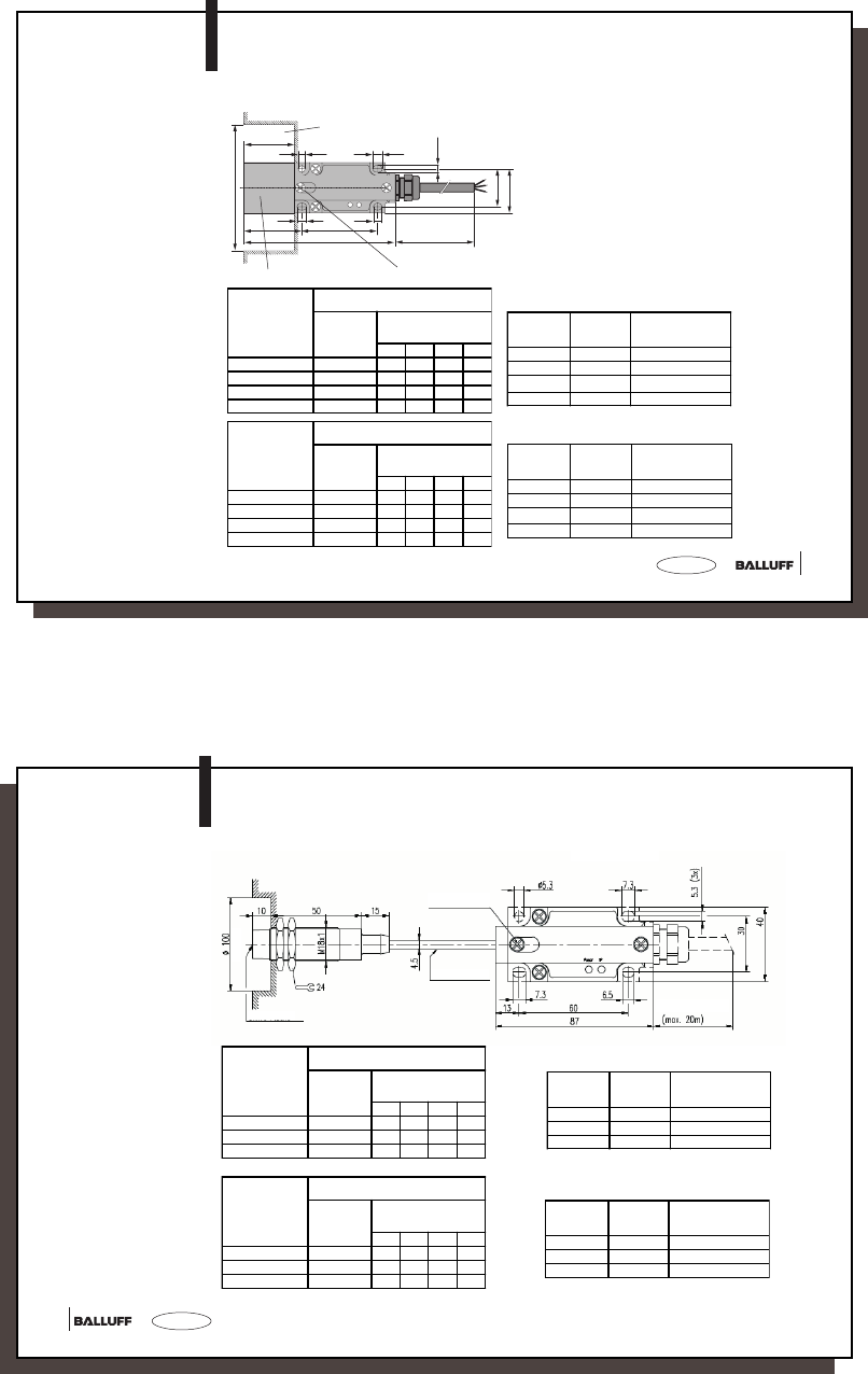
ø100
7.3
5.3 (3x)
60
46
120
6.5
40
Power T P
Clear zone
Set screwActive surface
L
Specificatio ns
used with data
carrier (installed in
clear zone)
For v = 0 (static mode)
Read
distance (mm)
Offset to center axis at
distance of: (mm)
0-25 0-35 0-45 0-15
BIS L-100-05 0 - 30 ± 15 -
BIS L-101-05 0 - 40 - ± 20 - -
BIS L-102-05 0 - 55 - - ± 30 -
BIS L-103-05 0 - 20 - - - ± 10
At read
distance
[mm]
Speed [m/s]
BIS L-200-03 15 0.4
BIS L-201-03 20 0.45
BIS L-202-03 27.5 0.5
BIS L-203-03 10 0.28
At read
distance
[mm]
Speed [m/s]
BIS L-100-05 15 0.45
BIS L-101-05 20 0.5
BIS L-102-05 27.5 0.72
BIS L-103-05 10 0.36
BIS L-405-03_-00_-05-MU_834487_E_0709.p65
18
english18
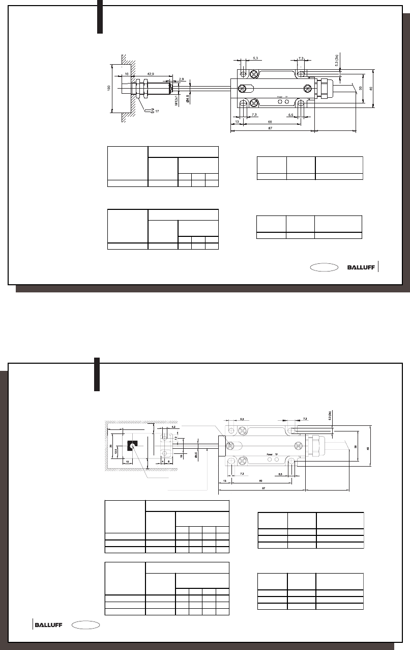
BIS L-405-...-002-...
Installation
Installation
BIS L-405-...-002-...
Specifications by
data carrier
BIS L-405-037-002-...
Specifications by
data carrier
BIS L-405-033-002-...
Specificatio ns by
data carrier
(installed in clear
zone)
For v = 0 (static condition)
Read
distance (mm)
Offset to center axis at
distance of: (mm)
0-10 0-15 0-20 0-25
BIS L-200-03 0 -23 ± 12 ± 12 ± 8 -
BIS L-201-03 0 - 27 ± 15 ± 15 ± 15 ± 6
BIS L-203-03 0 - 16 ± 8 ± 4 - -
Speeds:
Specificatio ns by
data carrier
(installed in clear
zone)
For v = 0 (static condition)
Read
distance (mm)
Offset to center axis at
distance of: (mm)
0-10 0-15 0-20 0-25
BIS L-100-05 0 -23 ± 12 ± 12 ± 8 -
BIS L-101-05 0 - 27 ± 15 ± 15 ± 15 ± 6
BIS L-103-05 0 - 16 ± 8 ± 4 - -
Set screw
Cable length
50 cm
Active surface
Standard length 5 m
Clear zone
At read
distance
[mm]
Speed [m/s]
BIS L-200-03 11.5 0.18
BIS L-201-03 13.5 0.22
BIS L-203-03 8 0.15
At read
distance
[mm]
Speed [m/s]
BIS L-100-05 11.5 0.22
BIS L-101-05 13.5 0.3
BIS L-103-05 8 0.18
19
19
english
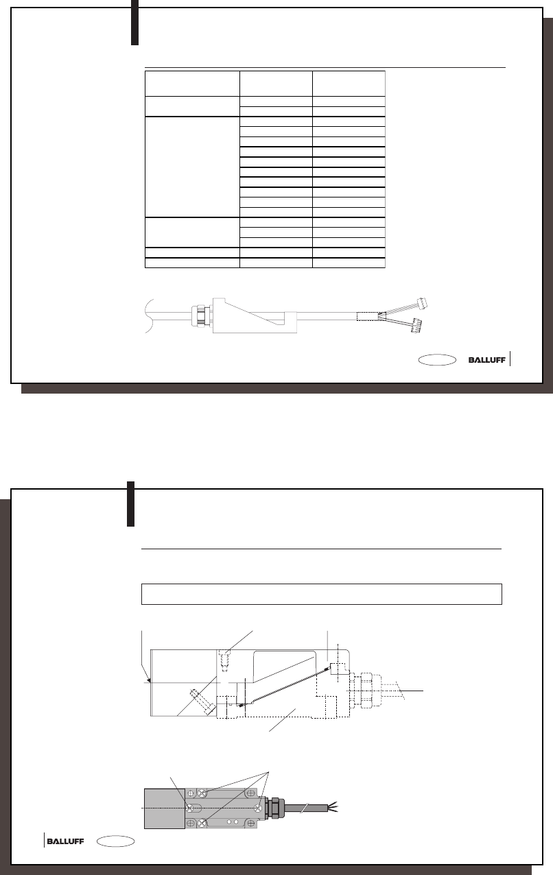
BIS L-405-...-003-...
Installation
Installation
BIS L-405-...-003-...
Specifications by
data carrier
BIS L-405-037-003-...
Specificatio ns by
data carrier
(installed i n clear
zone)
For v = 0 (static condition)
Read
distance (mm)
Offset to center
axis at distance of:
(mm)
0-5 0-8 0-11
BIS L-103-05 0 - 11 ± 6 ± 4 ± 2
Specifications by
data carrier
BIS L-405-033-003-...
Specificatio ns by
data carrier
(installed i n clear
zone)
For v = 0 (static condition)
Read
distance (mm)
Offset to center
axis at distance of:
(mm)
0-5 0-8 0-11
BIS L-203-03 0 - 11 ± 6 ± 4 ± 2
Speeds:
Standard length 5 m
(max. 20 m)
At read
distance
[mm]
Speed [m/s]
BIS L-203-03 51.5 0.11
At read
distance
[mm]
Speed [m/s]
BIS L-103-05 5.5 0.14
BIS L-405-03_-00_-05-MU_834487_E_0709.p65
20
english20
Installation
BIS L-405-...-004-...
Specifications by
data carrier
BIS L-405-037-004-...
Specifications by
data carrier
BIS L-405-033-004-...
BIS L-405-...-004-...
Installation
Specificatio ns by
data carrier
(installed in clear
zone)
For v = 0 (static condition)
Read
distance (mm)
Offset to center axis at
distance of: (mm)
0-10 0-15 0-20 0-25
BIS L-100-05 0 -23 ± 12 ± 12 ± 8 -
BIS L-101-05 0 - 27 ± 15 ± 15 ± 15 ± 6
BIS L-103-05 0 - 16 ± 8 ± 4 - -
Specificatio ns by
data carrier
(installed in clear
zone)
For v = 0 (static condition)
Read
distance (mm)
Offset to center axis at
distance of: (mm)
0-10 0-15 0-20 0-25
BIS L-200-03 0 -23 ± 12 ± 12 ± 8 -
BIS L-201-03 0 - 27 ± 15 ± 15 ± 15 ± 6
BIS L-203-03 0 - 16 ± 8 ± 4 - -
Speeds:
At read
distance
[mm]
Speed [m/s]
BIS L-200-03 11.5 0.18
BIS L-201-03 13.5 0.22
BIS L-203-03 8 0.15
At read
distance
[mm]
Speed [m/s]
BIS L-100-05 11.5 0.22
BIS L-101-05 13.5 0.3
BIS L-103-05 8 0.18
Set screw
Active surface
Cable length 50 cm
Standard length 5 m
(max. 20 m)
Clear zone 50
Clear zone 50
Clear zone 50
21
21
english
BIS L-405
Installation
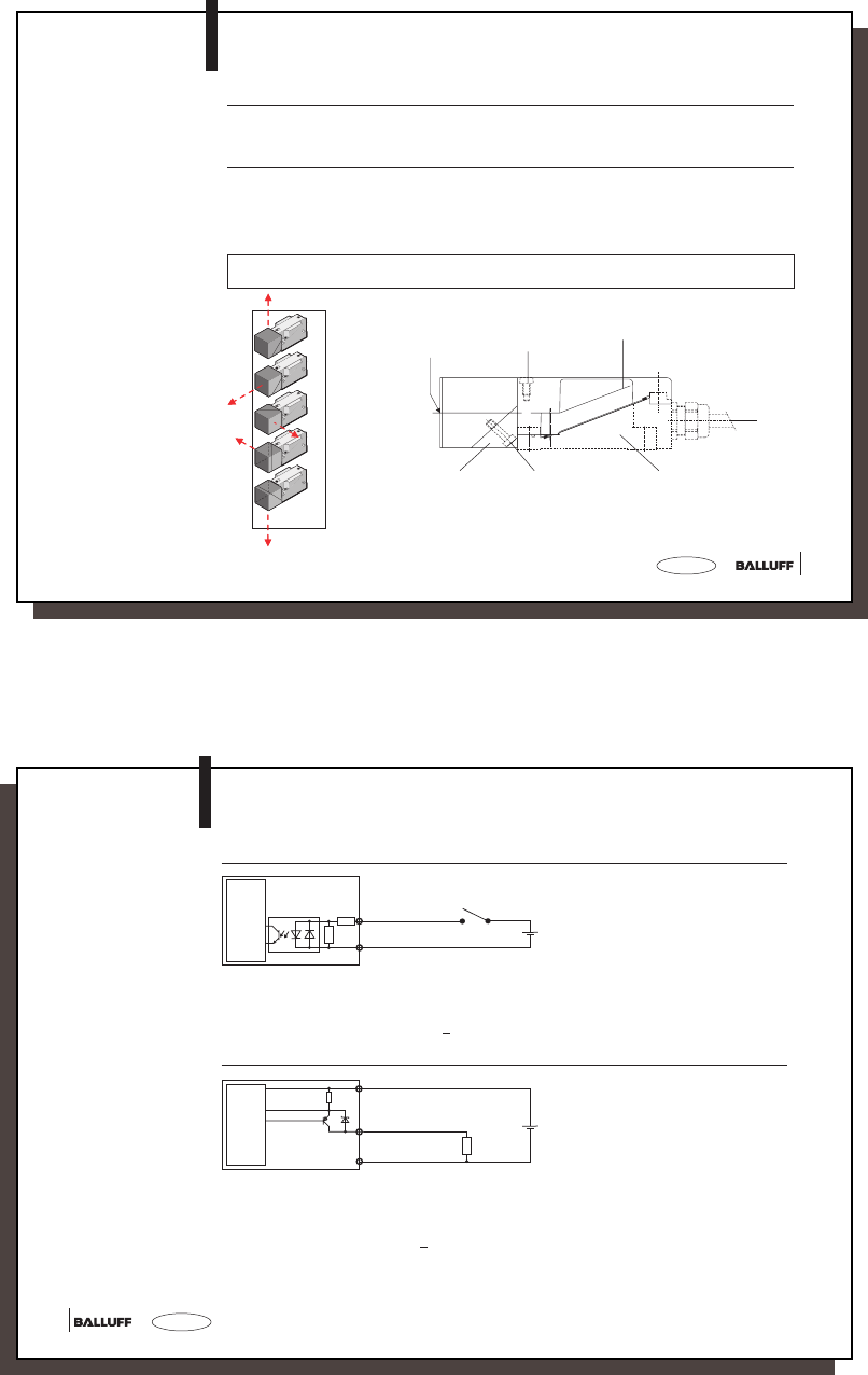
Lead assignments
BIS L-503-... Connection for Description Color
SUPPLY VOLTAGE +24 V DC RED
0 V DC BLUE
OUTPUTS
Bit 0 WHITE
Bit 1 BROWN
Bit 2 GREEN
Bit 3 YELLOW
Bit 4 GRAY
Bit 5 ROSE
Bit 6 BLACK
Bit 7 VIOLET
TP WHITE/GREEN
STR BROWN/GREEN
INPUTS
0V WHITE/YELLOW
ReStart GRAY/ROSE
ADR RED/BLUE
SHIELDING SHIELD -
n/c - YELLOW/BROWN
BIS L-405-03_-00_-05-MU_834487_E_0709.p65
22
english22
BIS L-405
Installation
When installing BIS L-405 and BIS L-503, remove the PG fitting. Insert BIS L-503 plug into
the correct sockets of the BIS L-405. Tighten screws and PG fitting.
Remove PG fitting before opening BIS L-405 and BIS L-503.
Installing the
BIS L-405 Processor
☞
Active surface Set screw BIS L405 module
BIS L-503 mounting base
Power TP
Set screw Screws for fastening
mounting base
23
23
english
BIS L-405
Reorienting and Rotating the Read Head
Reorienting the read
head
- Remove the two screws on the read head base
- Turn the read head module 180°
- Tighten both screws
- Unscrew the set screw
- Read head module can be rotated stepless (complete with read head base) to the
desired position (range: 270°)
- Tighten set screw
- Read head module is secured against over-rotation
Rotating the read
head
Read head modules are not interchangeable!
Active surface
positions
☞
Read head
base
Screw
Active
surface
Set screw BIS L405 module
BIS L-503
mounting base
Read head
module
BIS L-405-03_-00_-05-MU_834487_E_0709.p65
24
english24
BIS L-405
Connection Diagrams
Wiring the inputs
Wiring the outputs
for data
DC+24 V
–
ADR, ReStart
DC+24 V
–
D0...D 7, STR, TP
Load
Opto-
coupler
Supply voltage: DC 24 V +10% / –20% (incl. ripple)
Input high: min. 17 V, typ. 3 mA
Input low: max. 6 V, < 1.5 mA
Supply voltage: DC 24 V +10% / –20% (incl. ripple)
Output current: max. 50 mA
Voltage drop at 50 mA: < 1.5 V
25
25
english
General data Housing Plastic (PBT)
Ambient temperature 0 °C to +60 °C
Enclosure rating IP 67 (only when assembled)
Supply voltage DC 24 V +10 % / –20 % (incl. ripple)
Current consumption ≤ 50 mA with no load
Output current per output max. 50 mA
Power LED green
Tag Present LED yellow
Overflow LED yellow flashing
(The "Tag Present" LED flashes rapidly if the data
from a data carrier were not completely read and a
new data carrier has arrived in the active zone.)
BIS L-405
Technical Data
Temperature range
Enclosure rating
Supply voltage
The CE Marking verifies that our products conform to the requirements of the
EU Directive
2004/108/EC (EMC Directive)
and the EMC Law. In our EMC Laboratory, which is accredited by the DATech for Testing
Electromagnetic Compatibility, we have verified that Balluff products meet the EMC re-
quirements of the following Generic Standards:
EN 61000-6-4 (Emission), EN 61000-6-2 (Noise Immunity).
LED function
indicator
BIS L-405-03_-00_-05-MU_834487_E_0709.p65
26
english26
Balluff Identification System
Series L
Hardware-Type
405 = Plastic housing
Software-Type
033 = 8 bits parallel
037 = 8 bits parallel with CRC_16 data check
Hardware version
001 = Coil Ø 34 mm
002 = discharged read head modules M18 (0.5 m cable)
003 = discharged read head modules M12 (0.5 m cable)
004 = discharged read head modules C-305 housing (0.5 m cable)
Interface
05 = parallel
Module
MU = Module unit
Used only together with mounting base BIS L-503-PU1-...
BIS L-405-03_-00_-05-MU
BIS L-405
Ordering Information
Part Numbers
Read head modules are not interchangeable!
☞
27
27
english
Appendix, ASCII Table
Deci-
mal Hex Control
Code ASCII Deci-
mal Hex Control
Code ASCII Deci-
mal Hex ASCII Deci-
mal Hex ASCII Deci-
mal Hex ASCII Deci-
mal Hex ASCII
0 00 Ctrl @ NUL 22 16 Ctrl V SYN 44 2C , 65 41 A 86 56 V 107 6B k
1 01 Ctrl A SOH 23 17 Ctrl W ETB 45 2D - 66 42 B 87 57 W 108 6C l
2 02 Ctrl B STX 24 18 Ctrl X CAN 46 2E . 67 43 C 88 58 X 109 6D m
3 03 Ctrl C ETX 25 19 Ctrl Y EM 47 2F / 68 44 D 89 59 Y 110 6E n
4 04 Ctrl D EOT 26 1A Ctrl Z SUB 48 30 0 69 45 E 90 5A Z 111 6F o
5 05 Ctrl E ENQ 27 1B Ctrl [ ESC 49 31 1 70 46 F 91 5B [ 112 70 p
6 06 Ctrl F ACK 28 1C Ctrl \ FS 50 32 2 71 47 G 92 5C \ 113 71 q
7 07 Ctrl G BEL 29 1D Ctrl ] GS 51 33 3 72 48 H 93 5D ] 114 72 r
8 08 Ctrl H BS 30 1E Ctrl ^ RS 52 34 4 73 49 I 94 5E ^ 115 73 s
9 09 Ctrl I HT 31 1F Ctrl _ US 53 35 5 74 4A J 95 5F _ 116 74 t
10 0A Ctrl J LF 32 20 SP 54 36 6 75 4B K 96 60 ` 117 75 u
11 0B Ctrl K VT 33 21 ! 55 37 7 76 4C L 97 61 a 118 76 v
12 0C Ctrl L FF 34 22 " 56 38 8 77 4D M 98 62 b 119 77 w
13 0D Ctrl M CR 35 23 # 57 39 9 78 4E N 99 63 c 120 78 x
14 0E Ctrl N SO 36 24 $ 58 3A : 79 4F O 100 64 d 121 79 y
15 0F Ctrl O SI 37 25 % 59 3B ; 80 50 P 101 65 e 122 7A z
16 10 Ctrl P DLE 38 26 & 60 3C < 81 51 Q 102 66 f 123 7B {
17 11 Ctrl Q DC1 39 27 ' 61 3D = 82 52 R 103 67 g 124 7C |
18 12 Ctrl R DC2 40 28 ( 62 3E > 83 53 S 104 68 h 125 7D }
19 13 Ctrl S DC3 41 29 ) 63 3F ? 84 54 T 105 69 i 126 7E ~
20 14 Ctrl T DC4 42 2A * 64 40 @ 85 55 U 106 6A j 127 7F DEL
21 15 Ctrl U NAK 43 2B +
BIS L-405-03_-00_-05-MU_834487_E_0709.p65