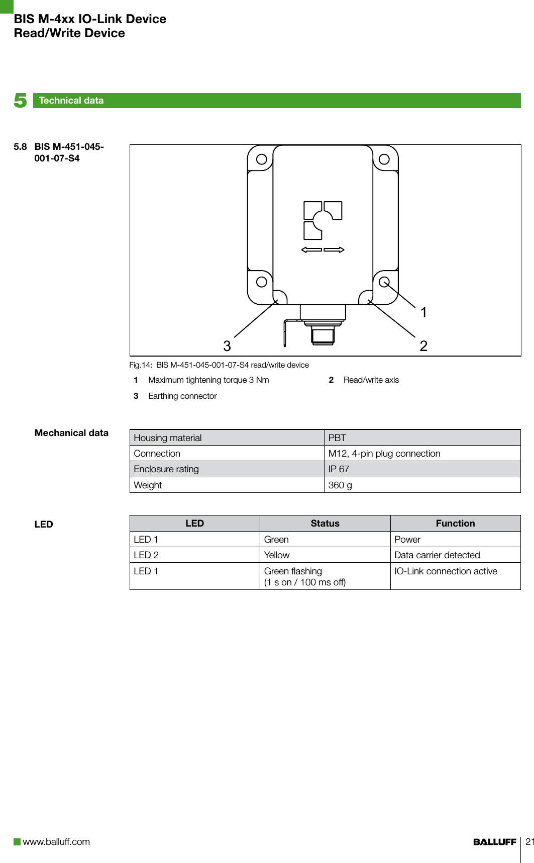
Balluff BISM4XX07 RFID Read-only, non-contact User Manual 1 of 2
Balluff Inc RFID Read-only, non-contact 1 of 2
UserManual.wiki
>
Balluff
>
BISM4XX07 User Manual
>
User Manual 1 of 2.pdf
Contents
1.
User Manual 1 of 2.pdf
2.
User Manual 2 of 2.pdf
User Manual 1 of 2.pdf
Navigation menu
Upload a User Manual
Namespaces
Wiki Guide
HTML
PDF
Info
Views
User Manual
Discussion / Help
Navigation

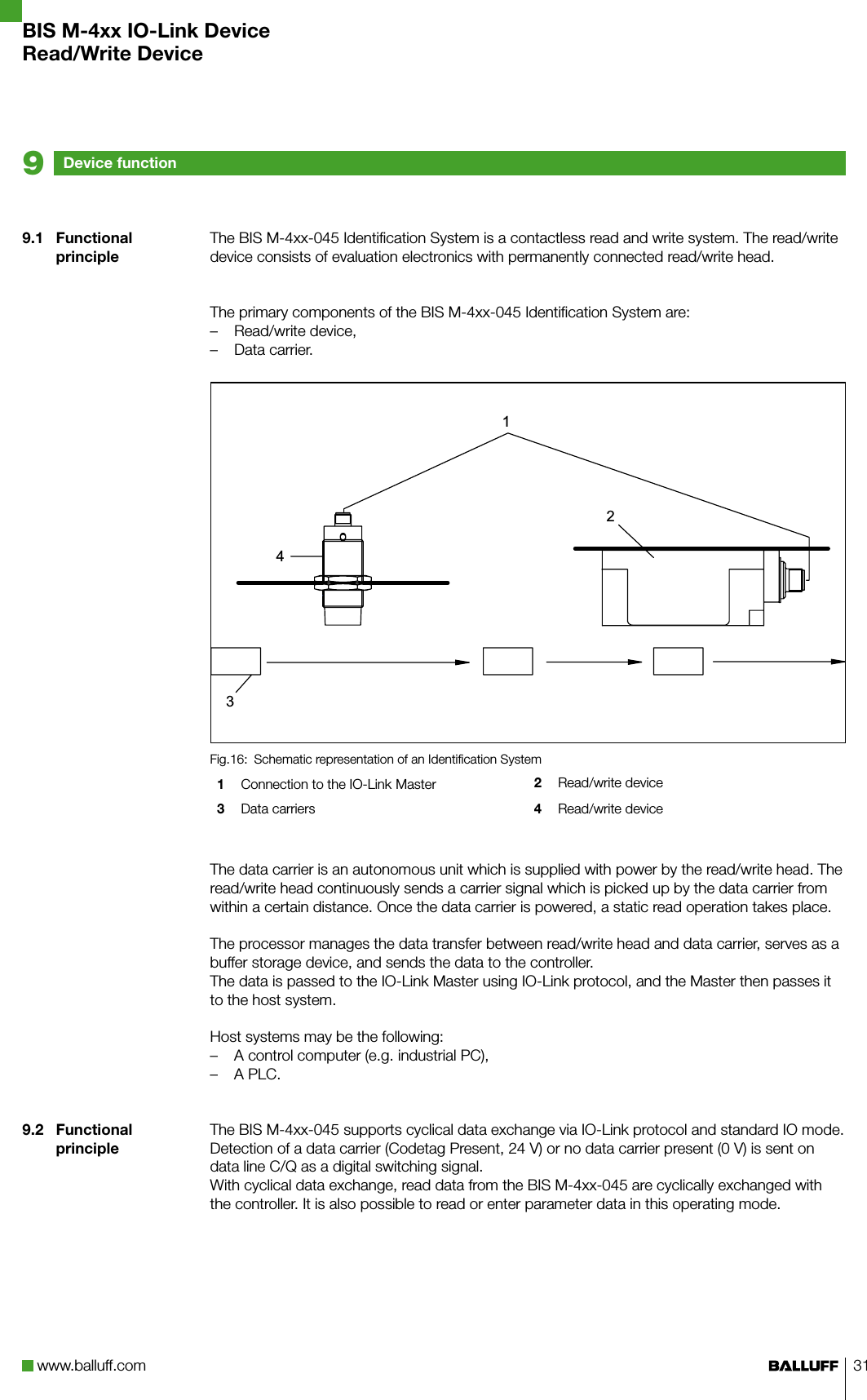
![22The read/write device can read or write each individual byte on the data carrier. But since the data carrier is divided into 16-byte memory blocks, the actual writing can only be performed in blocks. Our processor electronics convert this time accordingly.To calculate the read/write times, the block read or write time must, therefore, always be estima-ted.Data-carrier detection time [mm]Parameter "Used data carrier type“All BIS M1xx-01 BIS M1xx-02BIS M1xx-02 data carrier ≤ 40 - ≤ 27BIS M1xx-01 data carrier ≤ 30 ≤ 18 -Data carrier with 16 byte blocks BIS M-1xx-01 BIS M-1xx-02First block to be read ≤ 20 ≤ 35Other started 16 bytes ≤ 10 ≤ 25Data carrier with 16 bytes per block BIS M-1xx-01 BIS M-1xx-02First block to be read ≤ 40 ≤ 65Other started 16 bytes ≤ 30 ≤ 55NoteFluctuations in the ms range are possible. Electrical noise effects may increase the read/write time.To calculate the permissible speed at which the data carrier and head may move relative to one another, the static distance values are used (see Chapter 5 "Technical data“, pages 16 to 23).The permissible speed is:Vmax. perm..Path 2 * |offset value|= =Time Processing timeThe offset value is dependent on the read/write distance actually used in the system.Processing time = Data-carrier detection time +Read/write time of first block to be read+ n1XRead/write time for other started blocks1 Number of started blocksTechnical data55.9 Dynamic modeMemory accessData carrier detection timeRead timesWrite timesMaximum speedBIS M-4xx IO-Link DeviceRead/Write Device](https://usermanual.wiki/Balluff/BISM4XX07.User-Manual-1-of-2-pdf/User-Guide-2977155-Page-22.png)
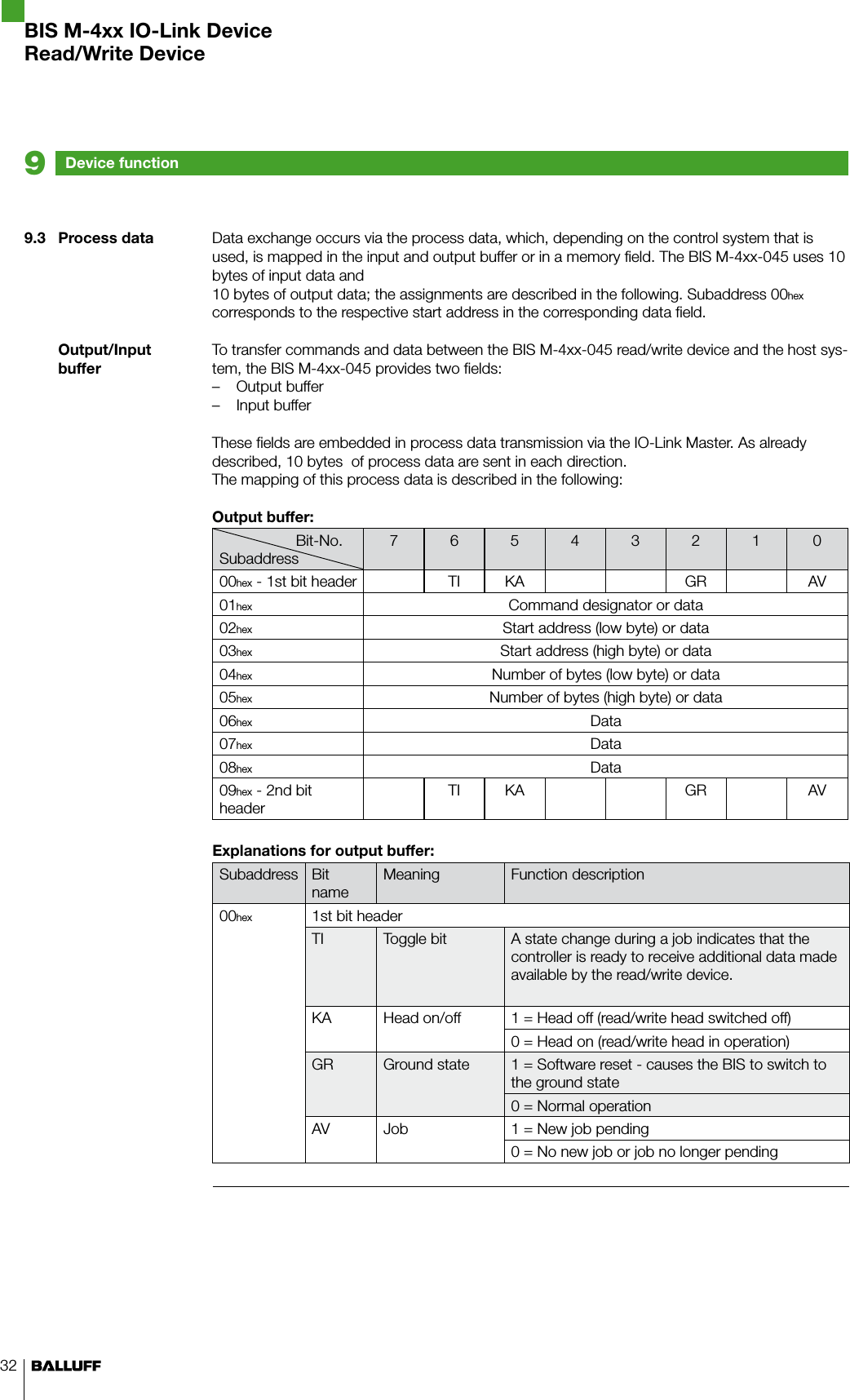
![28Action if tag presentStart address for autoreadData carrierBaud rateThe "Action on tag present" parameter specifies how the read/write device is to react if a new data carrier is detected in the field. The default setting is to send the UID (serial number). In addition, it is possible to set that nothing or a selected range of 8 bytes is to be sent immediately as read data. The following values are permissible:Index 40hex, subindex 3hex - 1 byte0hex No action1hex Send UID immediately7hex Immediately send 8 bytes of data beginning at a set address (parameter "Autoread start address“)This parameter is only valid if "Autoread“ was selected as the action on tag present. The start address can be set via subindices 4hex (low byte) and 5hex (high byte). The value range is depen-dent on the specification of the data carrier; take this into account. An incorrect setting prevents autoread from functioning; no data is output.This parameter offers the possibility of specifying certain data carrier models that are to be detected. All models, all BIS M1xx-01 models or all BIS M1xx-02 models can be selected. The data carriers are detected more quickly if only those that are used are parameterized. The fol-lowing values are permissible:Index 40hex, subindex 6hex - 1 byte0hex All data carrier models supported by BalluffFEhex All BIS M1xx-01 model data carriersFEhex All BIS M1xx-02 model data carriersThe Baud Rate parameter can be used to set the used transfer rate. The Min Cycle Time, i.e. the time intervals at which the device may be queried by the IO-Link Master, is dependent on the setting of this parameter. The following table applies:Index 41hex, subindex 1hex - 1 byteIO Link designationBaud Rate [baud]Parameter settingMin Cycle TimeCOM1 4800 00hex 60hex = 12.8 msCOM2 38400 01hex 35hex = 5.3 msCOM3 230400 02hex 20hex = 3.2 msNoteNot all IO-Link Masters support COM3. This must absolutely be checked before parameterizing! After the speed has been parameterized once, the device is only parameterized for this speed and can only be reparameterized using a COM3-capa-ble IO-Link Master. The Balluff-USB-Master is recommended for this purpose. Please contact Balluff Sales for further information.After saving the parameter, the M-4xx-045-... performs a reset. During this process, IO Link communication is interrupted and errors can be displayed in the controller. Only after this reset does the device restart with the newly set baud rate.Parameterizing the read/write device7BIS M-4xx IO-Link DeviceRead/Write Device](https://usermanual.wiki/Balluff/BISM4XX07.User-Manual-1-of-2-pdf/User-Guide-2977155-Page-28.png)
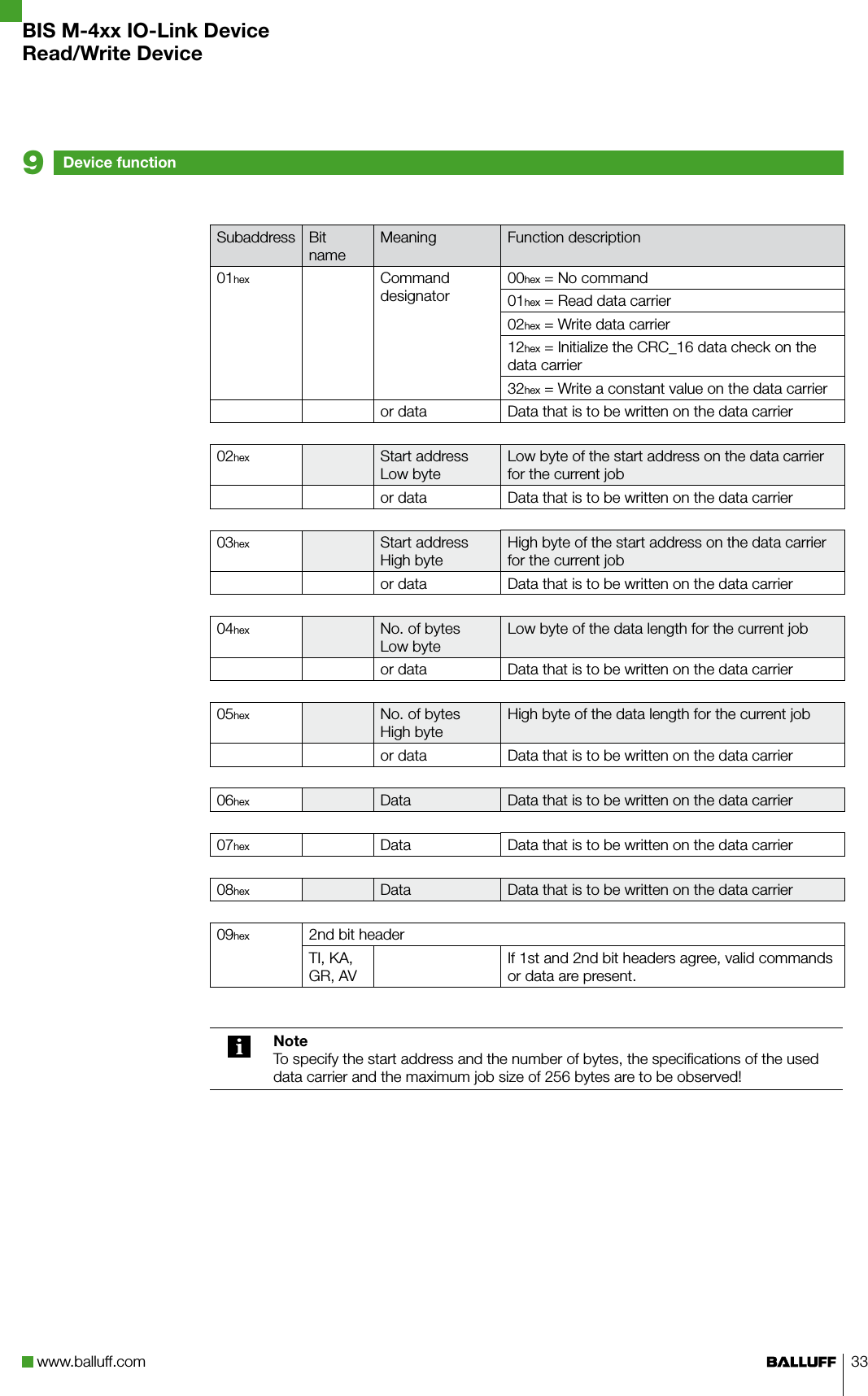
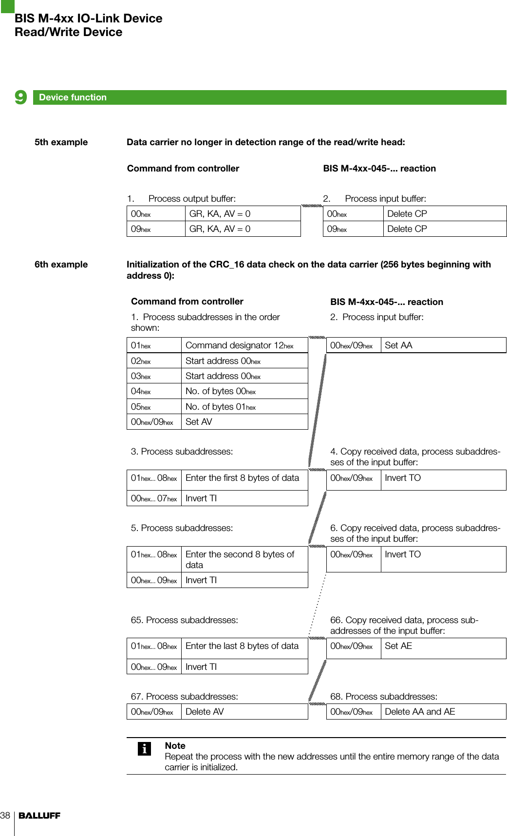
![48Decimal Hex Control codeASCII Decimal Hex ASCII Decimal Hex ASCII0 00 Ctrl @ NUL 43 2B + 86 56 V1 01 Ctrl A SOH 44 2C , 87 57 W2 02 Ctrl B STX 45 2D - 88 58 X3 03 Ctrl C ETX 46 2E . 89 59 Y4 04 Ctrl D EOT 47 2F / 90 5 A Z5 05 Ctrl E ENQ 48 30 0 91 5B [6 06 Ctrl F ACK 49 31 1 92 5C \7 07 Ctrl G BEL 50 32 2 93 5D [8 08 Ctrl H BS 51 33 3 94 5E ^9 09 Ctrl I HT 52 34 4 95 5F _10 0 A Ctrl J LF 53 35 5 96 60 `11 0B Ctrl K VT 54 36 6 97 61 A12 0C Ctrl L FF 55 37 7 98 62 B13 0D Ctrl M CR 56 38 8 99 63 c14 0E Ctrl N SO 57 39 9 100 64 d15 0F Ctrl O SI 58 3 A : 101 65 e16 10 Ctrl P DLE 59 3B ; 102 66 f17 11 Ctrl Q DC1 60 3C < 103 67 g18 12 Ctrl R DC2 61 3D = 104 68 h19 13 Ctrl S DC3 62 3E > 105 69 i20 14 Ctrl T DC4 63 3F ? 106 6 A j21 15 Ctrl U NAK 64 40 @ 107 6B k22 16 Ctrl V SYN 65 41 A 108 6C L23 17 Ctrl W ETB 66 42 B 109 6D m24 18 Ctrl X CAN 67 43 C 110 6E n25 19 Ctrl Y EM 68 44 D 111 6F o26 1 A Ctrl Z SUB 69 45 E 112 70 p27 1B Ctrl [ ESC 70 46 F 113 71 q28 1C Ctrl \ FS 71 47 G 114 72 r29 1D Ctrl ] GS 72 48 H 115 73 s30 1E Ctrl ^ RS 73 49 I 116 74 t31 1F Ctrl _ US 74 4 A J 117 75 u32 20 SP 75 4B K 118 76 V33 21 ! 76 4C L 119 77 W34 22 " 77 4D M 120 78 X35 23 # 78 4E N 121 79 Y36 24 $ 79 4F O 122 7 A Z37 25 % 80 50 P 123 7B {38 26 & 81 51 Q 124 7C |39 27 ‘ 82 52 R 125 7D }40 28 ( 83 53 S 126 7E ~41 29 ) 84 54 T 127 7F DEL42 2 A * 85 55 U ASCII tableAppendixBIS M-4xx IO-Link DeviceRead/Write Device](https://usermanual.wiki/Balluff/BISM4XX07.User-Manual-1-of-2-pdf/User-Guide-2977155-Page-48.png)