Balluff BISM4XX07 RFID Read-only, non-contact User Manual 1 of 2
Balluff Inc RFID Read-only, non-contact 1 of 2
Balluff >
Contents
- 1. User Manual 1 of 2.pdf
- 2. User Manual 2 of 2.pdf
User Manual 1 of 2.pdf
Technical Description, User's Guide
English
BIS M-4xx-045-00x-07-S4
www.balluff.com

www.balluff.com 3
8
7
6
5
4
3
2
1
9
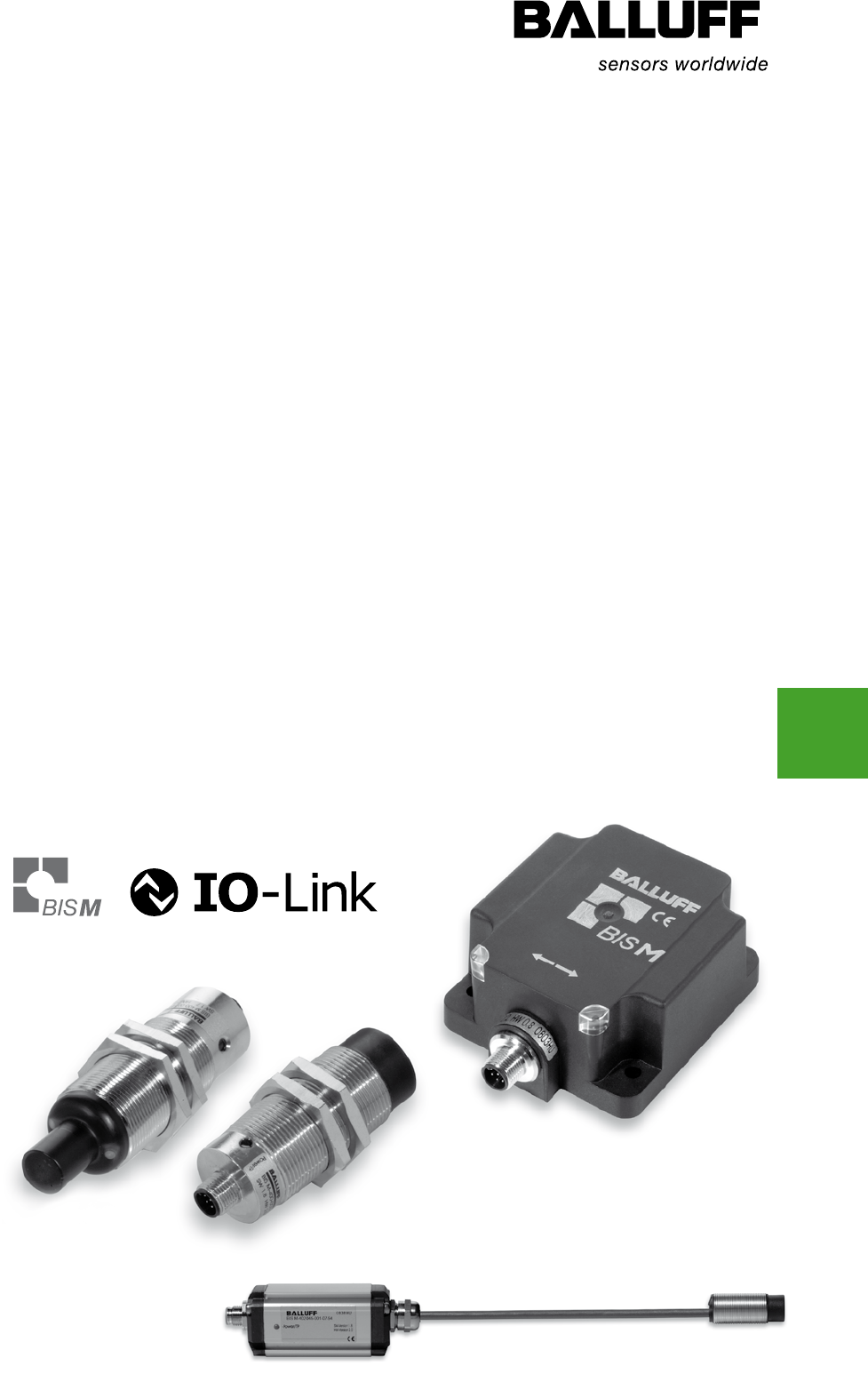
BIS M-4xx IO-Link Device
Read/Write Device
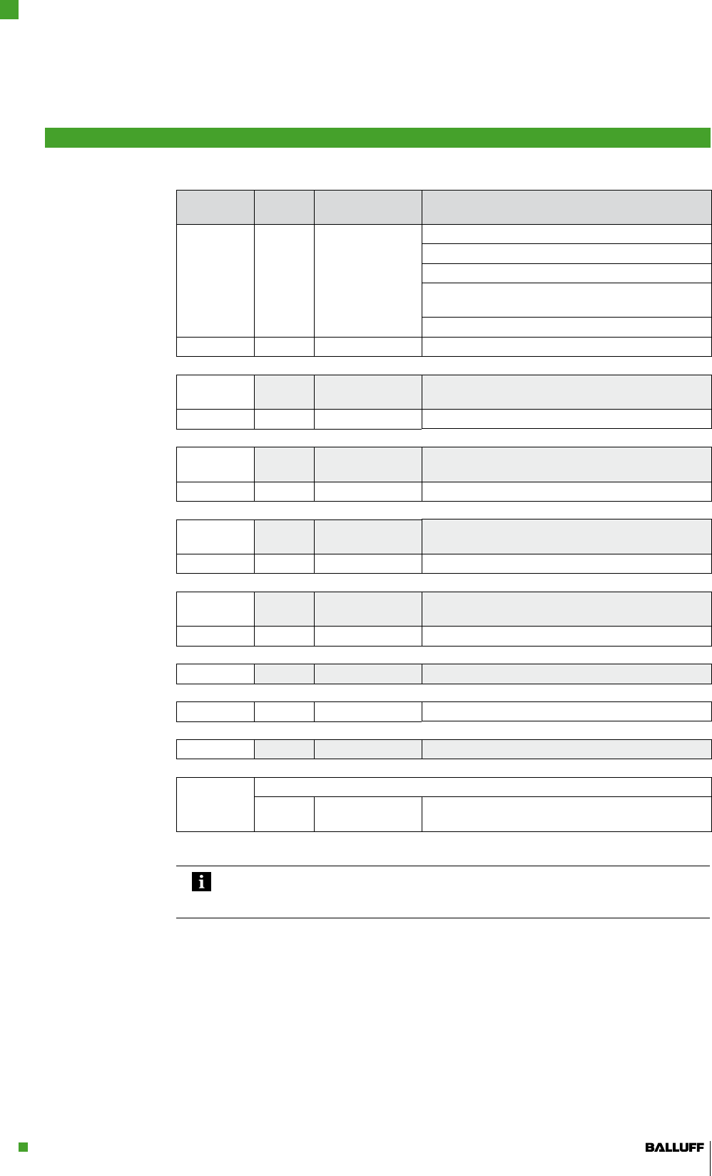
User instructions 5
1.1 Conformity and user safety 5
1.2 Scope of delivery 5
1.3 About this manual 5
1.4 Structure of the manual 5
1.5 Typographical conventions 5
1.6 Symbols 6
1.7 Abbreviations 6
Safety 7
2.1 Intended use 7
2.2 General safety notes 7
2.3 Meaning of the warnings 7
Getting started 8
3.1 Mechanical connection 8
3.2 Electrical connection 11
Basic knowledge 12
4.1 Function principle of Identification Systems 12
4.2 Example 13
4.3 Read distance/offset 14
4.4 Product description 14
4.5 Data integrity 14
4.6 Autoread 15
4.7 Supported data carrier types 15
4.8 IO-Link basic knowledge 15
Technical data 16
5.1 Electrical data 16
5.2 Operating conditions 16
5.3 BIS M-400-045-001-07-S4 16
5.4 BIS M-400-045-002-07-S4 17
5.5 BIS M-401-045-001-07-S4 18
5.6 BIS M-402-045-002-07-S4 19
5.8 BIS M-451-045-001-07-S4 21
5.9 Dynamic mode 22
IO-Link basics 24
6.1 Digital point-to-point connection 24
6.2 Process data container 25
6.3 Identificationdata and device information 25
Parameterizing the read/write device 26
7.1 Required data 26
7.2 Mapping of parameterization data 27
7.3 Storing the parameterization data 29
Startup 30
Device function 31
9.1 Functional principle 31
9.2 Functional principle 31
9.3 Process data 32


www.balluff.com 5
This product was developed and manufactured in accordance with applicable European stan-
dards and directives.
Declaration of Conformity
This product was developed and manufactured in accordance with applicable Euro-
pean standards and
directives.
Note
You can request a Declaration of Conformity separately.
For additional safety instruction, refer to Chapter "Safety“ on page 7.
UL listing
Control No. 3TLJ
File No. E227256
Included in the scope of delivery:
BIS M-4xx IO-Link device –
BIS software CD –
Condensed manual in printed form (DE, EN) –
This manual describes the read/write device of the BIS M-4xx-IO-Link Identification System and
includes startup instructions for immediate operation.
This manual does not describe:
The start-up, function and safe operation of the host device (PC, PLC, IO-Link Master). –
The installation and function of accessories and expansion devices. –
The manual is organized so that the sections build on each other.
Chapter 2: Basic safety information.
Chapter 3: The key steps for installing the Identification System.
Chapter 4: Introduction to the material.
Chapter 5: Technical data for the read/write device.
Chapter 6: Basics on the IO-Link communications standard.
Chapter 7: User-defined settings for the read/write device.
Chapter 8: Integration into a fieldbus system using Profibus as an example.
Chapter 9: Processor and host system interaction.
The following conventions are used in this manual.
Enumerations are shown as a list with an en-dash.
Entry 1, –
Entry 2. –
Action instructions are indicated by a preceding triangle. The result of an action is indicated by
an arrow.
1.1 Conformity and
user safety
1.2 Scope of delivery
1.3 About this
manual
1.4 Structure of the
manual
1.5 Typographical
conventions
Enumerations
Actions
User instructions
1
BIS M-4xx IO-Link Device
Read/Write Device
6
Action instruction 1. ►
Action result. ⇒
Action instruction 2. ►
Numbers:
Decimal numbers are shown without additional indicators (e.g. 123), –
Hexadecimal numbers are shown with the additional indicator – hex (e.g. 00hex).
Parameters:
Parameters are shown in italics (e.g. CRC_16).
Directory paths:
References to paths in which data are stored or are to be saved are shown in small caps (e.g.
Pr o j e c t :\Da t a ty P e s \Us e r De f i n e D ).
Cross-references indicate where additional information on the topic can be found (see "Technical
Data“ starting on page 16).
Attention!
This symbol indicates a safety instruction that absolutely must be followed.
Note, tip
This symbol indicates general notes.
BIS Balluff Identification System
CRC Cyclic Redundancy Code
DPP Direct Parameter Page
EMC Electromagnetic Compatibility
LSB Least Significant Bit
MSB Most Significant Bit
PC Personal Computer
SIO Standard IO
SPDU Service Protocol Data Unit
PLC Programmable Logic Controller
TCP Transmission Control Protocol
Syntax
Cross-references
1.6 Symbols
1.7 Abbreviations
User instructions
1
BIS M-4xx IO-Link Device
Read/Write Device

www.balluff.com 7
The BIS M-4xx-... read/write device, together with other components of the BIS M, form the
Identification System.
They may only be used for this purpose in an industrial environment corresponding to Class A of
the EMC law.
This description applies for the read/write devices of the BIS M-4xx-... series.
Installation and startup
Installation and startup are only to be performed by trained specialists. Any damage resulting
from unauthorized manipulation or improper use voids the manufacturer's guarantee and war-
ranty.
When connecting the read/write device to an external controller, pay attention to the choice and
polarity of the connection as well as the power supply.
The read/write device must only be powered using approved power supplies (see Chapter 5
"Technical data" beginning on page 16).
Attention!
This is a Class A device. This device may cause RF disturbances in residential areas;
in such a case the operator may be required to take appropriate countermeasures.
Operation and testing
The operator is responsible for ensuring that locally applicable safety regulations are observed.
In the event of defects and non-correctable faults in the Identification System, take the system
out of service and secure it from unauthorized use.
Attention!
The pictogram used with the word "Attention" warns of a possible hazardous situation
affecting the health of persons or equipment damage. Failure to observe these
warning notes may result in injury or damage to equipment.
Always observe the described measures for preventing this danger. ►
2.1 Intended use
2.2 General safety
notes
2.3 Meaning of the
warnings
Safety
2
BIS M-4xx IO-Link Device
Read/Write Device
8
3.1 Mechanical
connection
BIS M-400-...-001
BIS M-400-...-002
Getting started
3
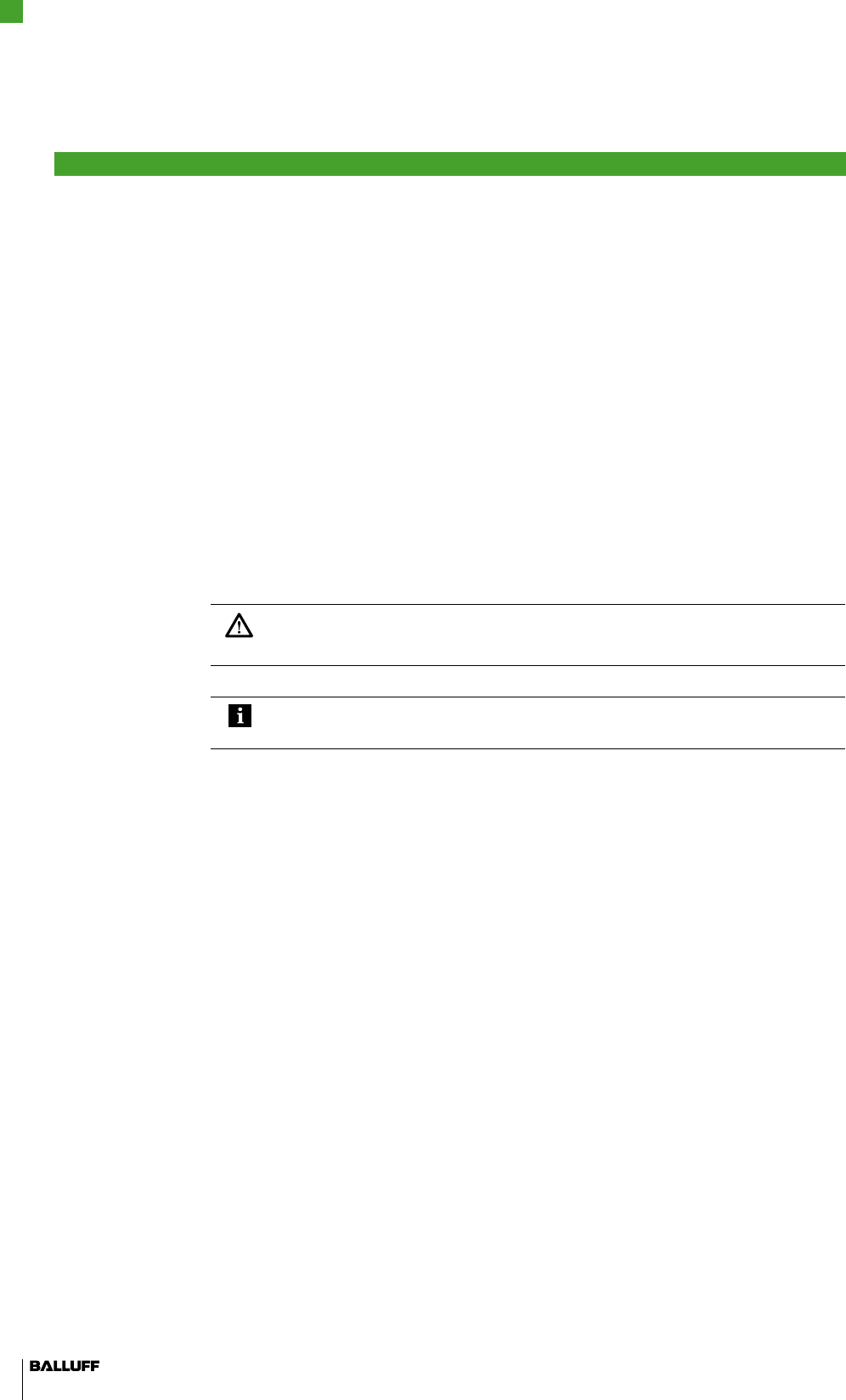
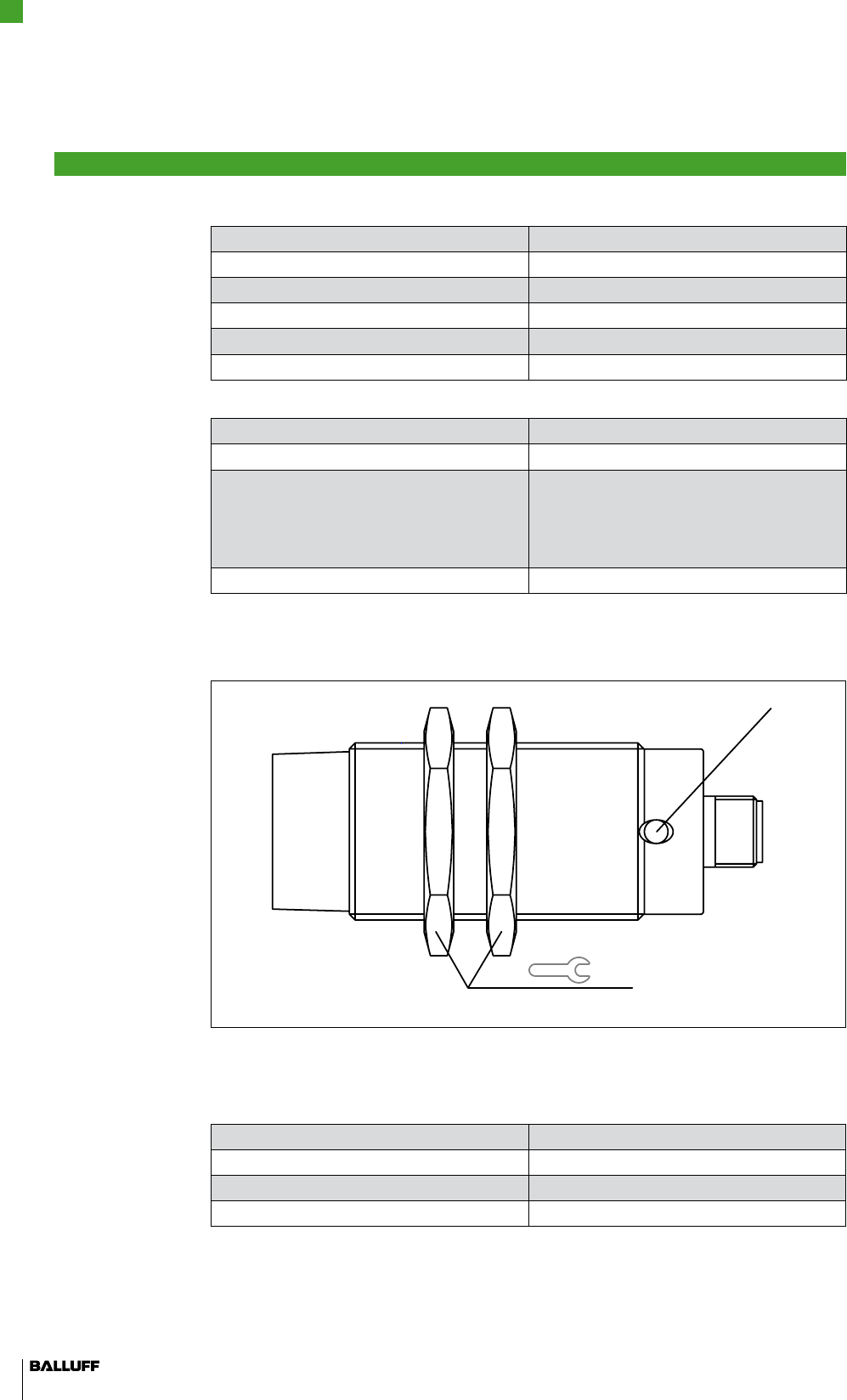
BIS M-400-045-001-07-S4 read/write device, values in mmFig.1:
1 Maximum tightening torque 40 Nm 2 Sensing surface
BIS M-400-045-002-07-S4 read/write device, values in mmFig.2:
1 Maximum tightening torque 40 Nm 2 Sensing surface
BIS M-4xx IO-Link Device
Read/Write Device
www.balluff.com 9
BIS M-401-...-001
BIS M-402-...-002
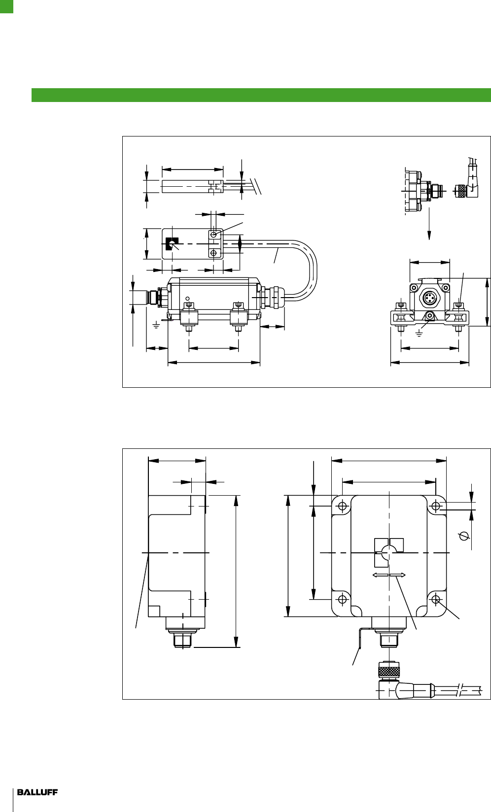
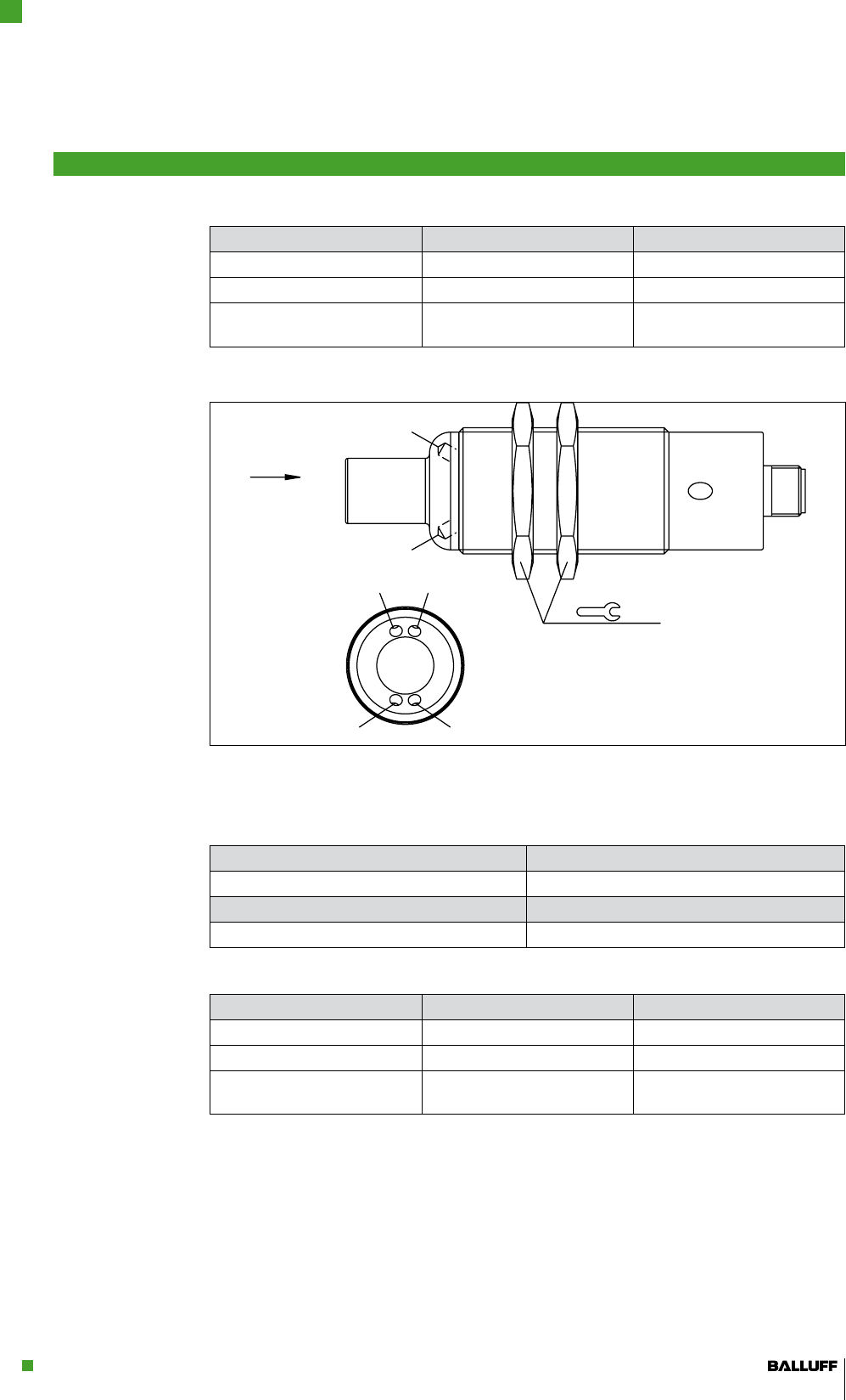
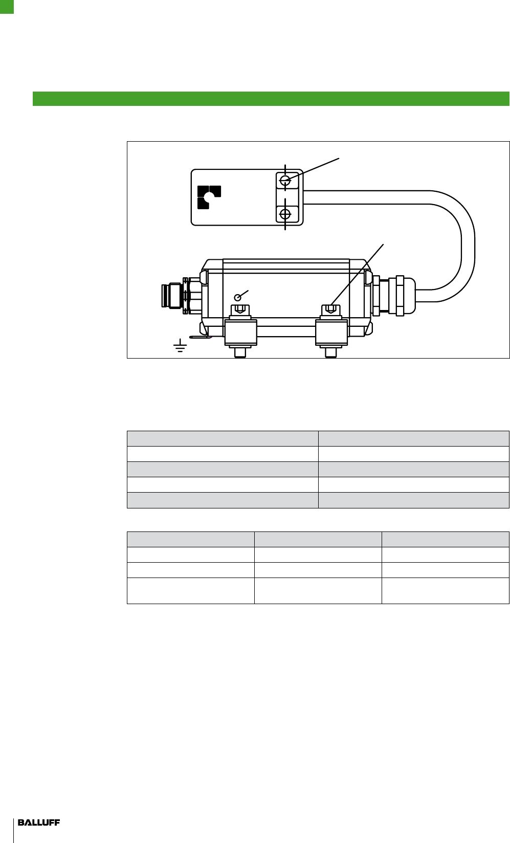
BIS M-401-045-001-07-S4 read/write device, values in mmFig.3:
1 Maximum tightening torque 3 Nm 2 Earthing connector
3 Sensing surface
BIS M-402-045-002-07-S4 read/write device, values in mmFig.4:
1 Sensing surface 2 Maximum tightening torque 25 Nm
3 Cable length 0.5 m 4 Maximum tightening torque 2 Nm
0
[
0
[
A
A
Getting started
3
BIS M-4xx IO-Link Device
Read/Write Device
10
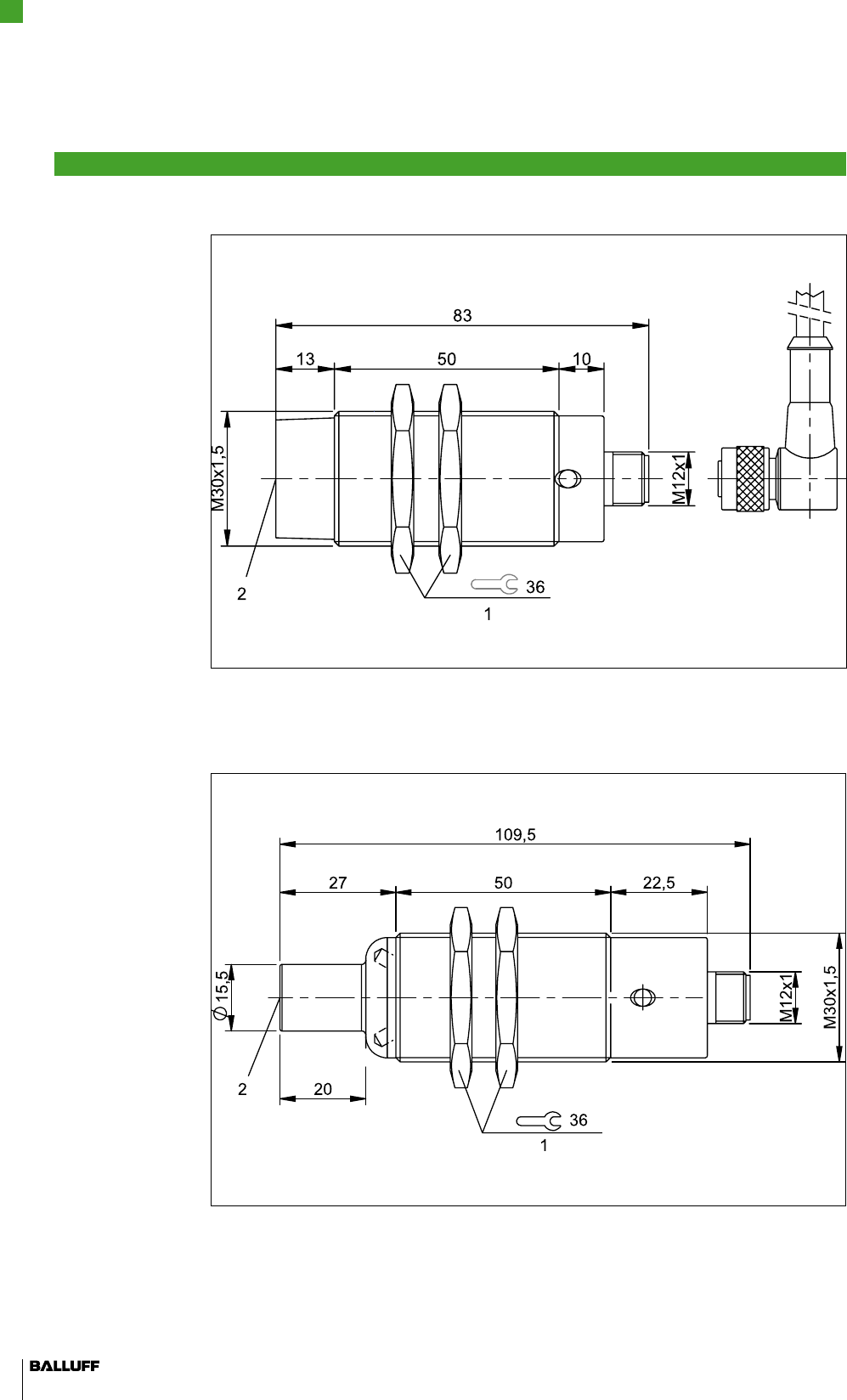
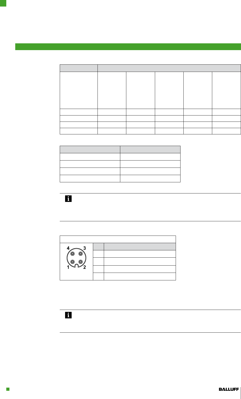
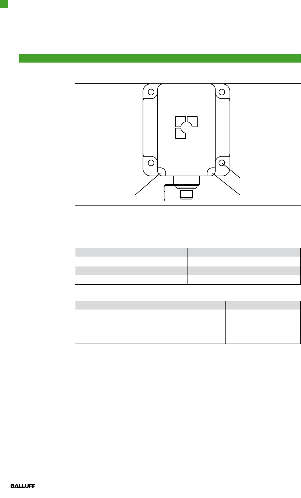
BIS M-402-045-004-07-S4 read/write device, values in mmFig.5:
1 Sensing surface 2 Maximum tightening torque 1 Nm
3 Cable length 0.5 m 4 Maximum tightening torque 2 Nm
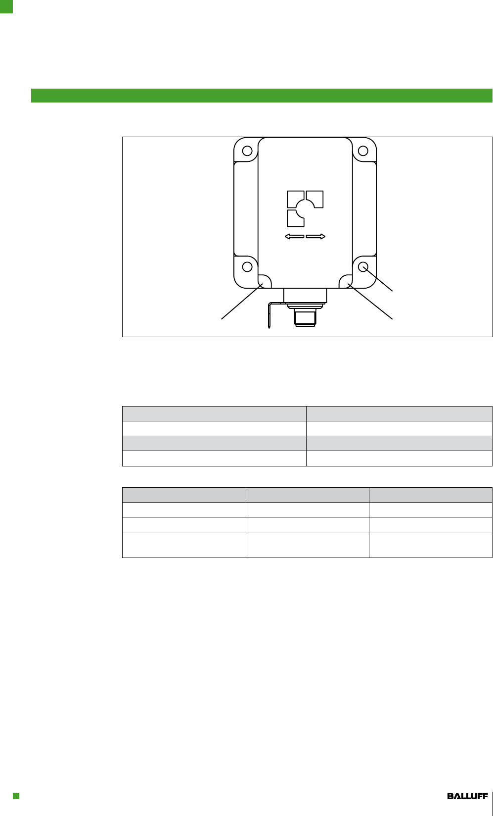
BIS M-451-045-001-07-S4 read/write device, values in mmFig.6:
1 Maximum tightening torque 3 Nm 2 Read/write axis
3 Earthing connector 4 Sensing surface
0
[
A
A
BIS M-402-...-004
BIS M-451-...-001
Getting started
3
BIS M-4xx IO-Link Device
Read/Write Device
www.balluff.com 11
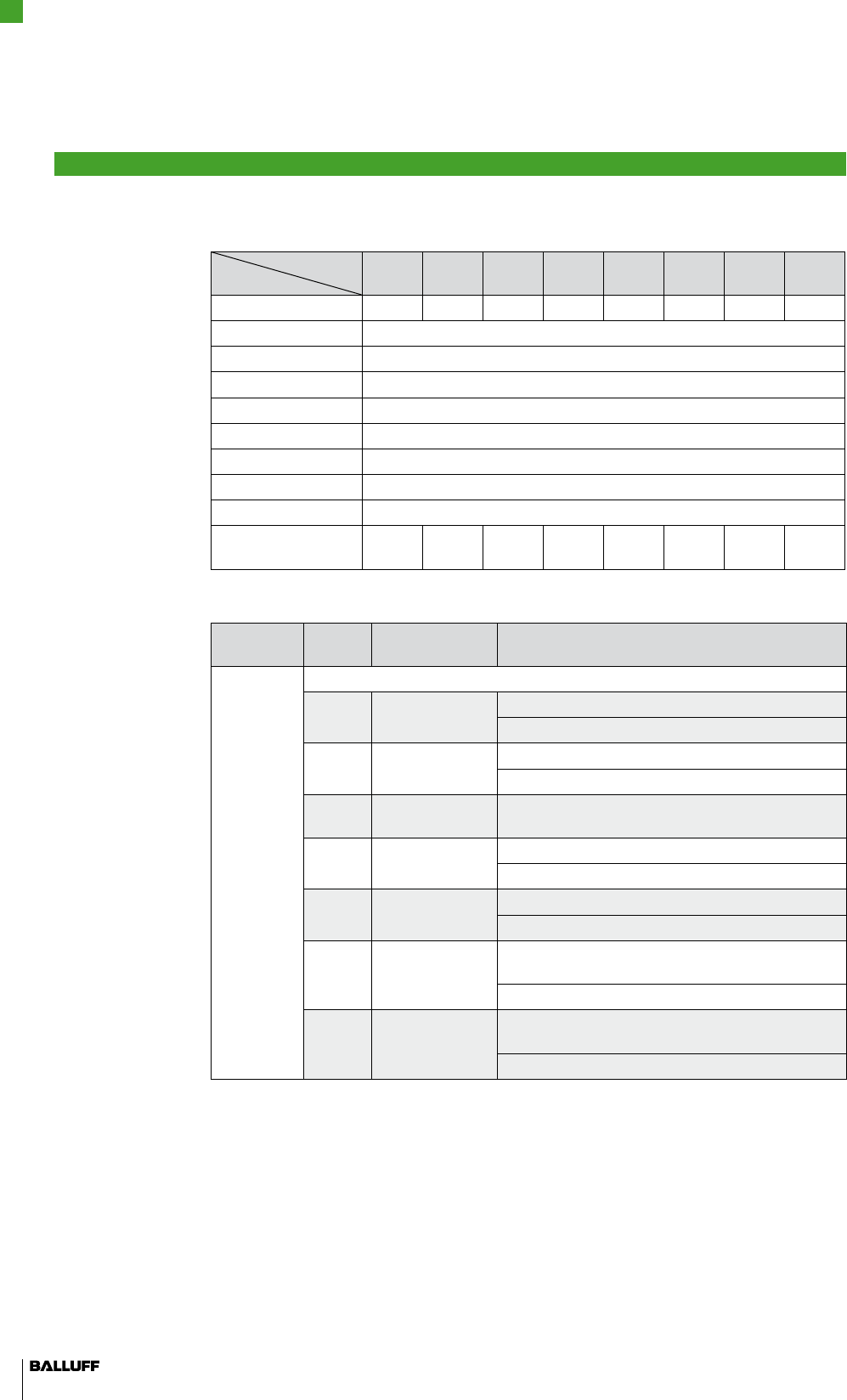
Data carrier Distance
BIS M-101-...
BIS M-106-...
BIS M-107-...
BIS M-108-...
BIS M-110-...
BIS M-111-...
BIS M-115-...
BIS M-102-...
BIS M-112-...
BIS M-105-...
BIS M-122-...
BIS M-120-... BIS M-150-...
BIS M-151-...
BIS M-400-045-... > 10 cm > 15 cm > 10 cm – –
BIS M-401-045-... > 20 cm > 20 cm – > 25 cm –
BIS M-402-045-... > 10 cm – > 10 cm – –
BIS M-451-045-... – – – – > 25 cm
Read/write device Minimum distance
BIS M-400-045-0xx-... 20 cm
BIS M-401-045-001-... 60 cm
BIS M-402-045-001-... 20 cm
BIS M-451-045-001-... 60 cm
Note
When installing two BIS M-4xx-...on metal, there is normally no mutual interference.
Unfavorable use of a metal frame can result in problems when reading a data carrier.
In this case, the read distance is reduced to 80% of the maximum value.
In critical applications, a pre-test is recommended.
IO-Link port (M12, A-coded, female)
PIN Function
1 +24 V
2 NC
3 GND
4 C/Q
Connect data line to IO-Link Master. ►
(See Balluff IO-Link catalog for connection cable and accessories)
Shielded cables are recommended in electromagnetically distorted environments.
Note
For all variants, the ground connection of the read/write device or of the function
ground are, depending on the system, to be connected to ground either directly / with
low impedance or via a suitable RC combination.
Distance
between the data
carriers
Distance
between the
read/write
devices
3.2 Electrical
connection
Getting started
3
BIS M-4xx IO-Link Device
Read/Write Device
12
4.1 Function
principle of
Identification
Systems
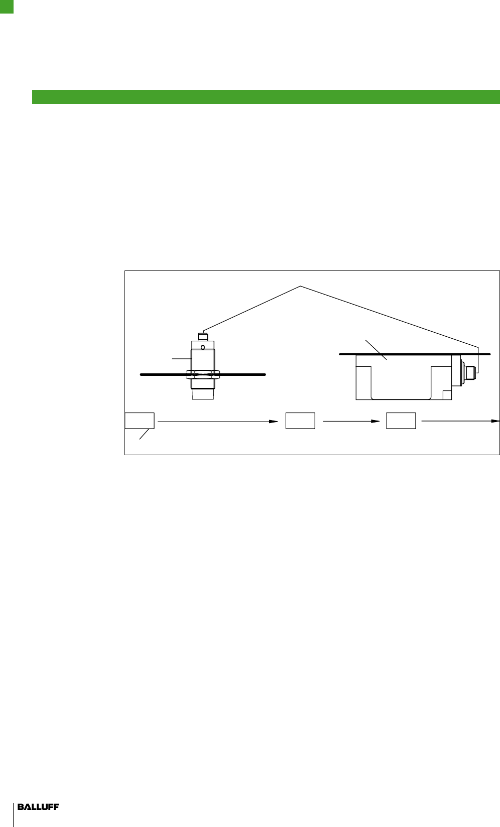
The BIS M-4xx-045 Identification System is a contactless read and write system. The read/write
device consists of evaluation electronics with permanently connected read/write head. The
system can be used to program and to read information on a data carrier. The data and current
status messages are transmitted from the Identification System to the host system via a defined
protocol. This protocol can also be used to transmit additional commands to the device, such as
switching off the read-head antenna.
The primary components of the BIS M-4xx-045 Identification System are:
Read/write device, –
Data carrier. –
Data is transmitted to the host system via an IO-Link Master.
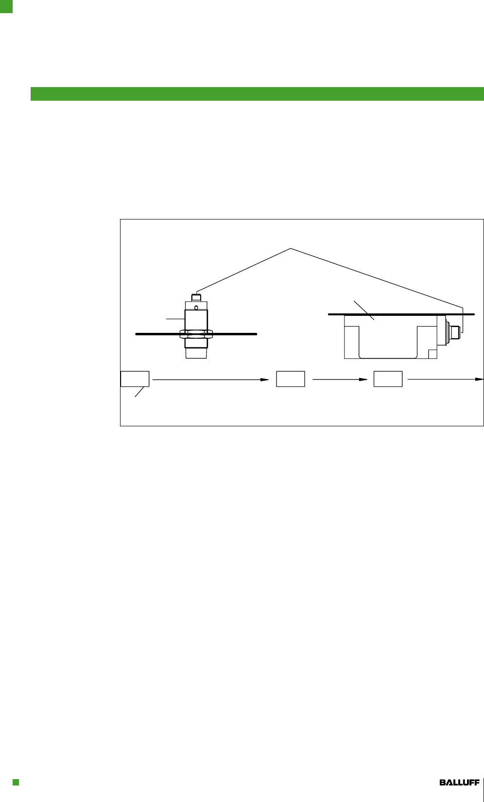
Schematic representation of an Identification SystemFig.7:
1 Connection to the IO-Link Master 2 Read/write device
3 Data carriers 4 Read/write device
The data carrier is an autonomous unit that is supplied with power by the read/write head. The
read/write head continuously sends a carrier signal that is picked up by the data carrier from
within a certain distance. As soon as the data carrier is powered up by the carrier signal, a static
read operation takes place.
The read/write device manages the data transfer between read/write head and data carrier,
serves as a buffer storage device, and sends the data to the host controller.
The data is passed to the IO-Link Master using IO-Link protocol, and the Master then passes it
to the host system.
Host systems may be the following:
a control computer (e.g. industrial PC), –
as PLC. –
The main areas of application are:
in production for controlling material flow (e.g. in model-specific processes, in workpiece –
transport with conveying systems, for acquiring safety-relevant data),
in warehousing for monitoring material movements, –
transportation, and –
conveying technology. –
Basic knowledge
4
BIS M-4xx IO-Link Device
Read/Write Device
www.balluff.com 13
Topology of a BIS M-4xx-045 Identification SystemFig.8:
1 PLC 2 PC
3 Fieldbus 4 IO-Link Master
5 Connection to the host system 6 BIS M-4xx-045 read/write device
1
3
4
5
6
2
4.2 Example
Basic knowledge
4
BIS M-4xx IO-Link Device
Read/Write Device

14
Basic knowledge
4
4.3 Read distance/
offset
4.4 Product
description
4.5 Data integrity
To ensure that data carriers are detected without error and the data can be reliably read, do not
exceed a maximum distance and maximum offset between the data carriers and read heads
(see Chapter 5 "Technical data“, page 16).
The "distance" value refers to the maximum distance from the data carrier to the sensing surface
of the read/write head.
The "offset" value indicates the maximum offset between the center axis of the data carrier and
the center axis of the sensing surface.
Data carriers can only be reliably detected and the data reliably read within the permissible read
distance and offset.
Data carrier detection is indicated by an LED on the device ("TP – Tag Present", see Chapter 5
"Technical data“, page 16). At the same time, the CP bit is set in the input buffer ("CP – Codetag
Present“, see Chapter 9.3 "Process data“, page 32).
BIS M-400-045-0xx-07-S4 read/write device:
M30 threaded tube, –
round connector terminations, –
integrated read/write head, –
the read/write head is suitable for dynamic or static operation, –
data carrier is powered by the read/write head using a carrier signal. –
BIS M-4x1-045-0xx-07-S4 read/write device:
plastic housing, –
round connector terminations, –
integrated read/write head, –
the read/write head is suitable for dynamic or static operation, –
data carrier is powered by the read/write head using a carrier signal. –
BIS M-402-045-0xx-07-S4 read/write device:
metal housing, –
round connector terminations, –
integrated read/write head, –
the read/write head is head suitable for dynamic or static operation, –
data carrier is powered by the read/write head using a carrier signal. –
read/write head in plastic (...-004-...) or metal housing (...-002-...). –
To ensure data integrity, data transfer between the data carrier and read/write device can be
monitored using a CRC_16 data check.
With the CRC_16 data check, a checksum is written to the data carrier which enables the data
to be checked for validity at any time.
Advantages of the CRC_16 data check:
Very high data integrity, even during the non-active phase (data carrier outside the read/write –
head)
Restrictions of the CRC_16 data check:
Longer write times, as the CRC must also be written. –
User bytes are lost on the data carrier – (see table on page 15).
Use of CRC_16 can be parameterized by the user (see Chapter 7 "Parameterizing the read/write
device“, page 26).
BIS M-4xx IO-Link Device
Read/Write Device

www.balluff.com 15
Basic knowledge
4
4.6 Autoread
4.7 Supported data
carrier types
4.8 IO-Link basic
knowledge
The Autoread function is used to immediately read out a specific memory area of the data carrier
when the data carrier enters the vicinity of the read head. The data quantity in this case is always
8 bytes; the start address can be parameterized.
If a read error occurs during autoread or if the specified data area lies outside the capacity of the
data carrier, no error is displayed. In this case, no data is output.
Mifare
Balluff data
carrier type
Manufac-
turer
Description Memory
capacity
Usable
bytes with
CRC
Memory
type
BIS M-1_ _-01 NXP Mifare Classic 752 bytes 658 bytes EEPROM
ISO15693
Balluff data
carrier type
Manufac-
turer
Description Memory
capacity
Usable
bytes with
CRC
Memory
type
BIS M-1_ _-02 Fujitsu MB89R118 2000 bytes 1750 bytes FRAM
BIS M-1_ _-03 NXP SL2ICS20 112 bytes 98 bytes EEPROM
BIS M-1_ _-04 Texas Inst. TAG-IT Plus 256 bytes 224 bytes EEPROM
BIS M-1_ _-05 Infineon SRF55V02P 224 bytes 196 bytes EEPROM
BIS M-1_ _-06 EM EM4135 288 bytes 252 bytes EEPROM
BIS M-1_ _-07 Infineon SRF55V10P 992 bytes 868 bytes EEPROM
BIS M-1_ _-08 NXP SL2IC553 160 bytes 140 bytes EEPROM
BIS M-1_ _-09 NXP SL2ICS50 32 bytes 28 bytes EEPROM
Advantages of IO-Link:
Uniform, simple wiring of different devices –
Host system can be used to change the device parameters –
Remote querying of diagnostic information is possible –
Centralized data retention of the device parameters is possible –
The manufacturer-specific standard IO-Link sends not only the actual process signal, but also all
relevant parameter and diagnostic data on the process level over a single standard cable.
Communication is based on a standard UART protocol with 24V pulse modulation; no separate
power supply is required.
The BIS M-4xx-045-... is an IO-Link device which uses three-conductor technology (Physics 2).
The transfer rate can be configured to 4800 (COM1), 38400 (COM2) or 230400 (COM3) baud.
The data quantity of the process data is 10 bytes in each direction (see Chapter 9 "Device
function“, page 31).
BIS M-4xx IO-Link Device
Read/Write Device
16
5.1 Electrical data
(valid for all
device versions)
5.2 Operating
conditions
(valid for all
device versions)
5.3 BIS M-400-045-
001-07-S4
Mechanical data
Technical data
5
Operating voltage VS18...30 VDC LPS/Class 2 supplied only
Ripple 1.3 Vss
Current draw 150 mA
Load current capacity in SIO mode Maximum 50 mA
Output C/Q Short-circuit protected
Device interface IO-Link
Storage temperature -20 °C … +85 °C
Ambient temperature 0 °C … +70 °C
EMC
EN 301 489-1/-3 –
EN 61000-4-2/-3/-4/-6 –
EN 300 330-1 –
Class B
Severity 2A/2A/4B*/XA**
Power Class 5
Vibration/shock EN 60068 Part 2 6/27/29/64/32
*For 230.4 kBaud, use shielded cable.
**Verified with shielded cable.
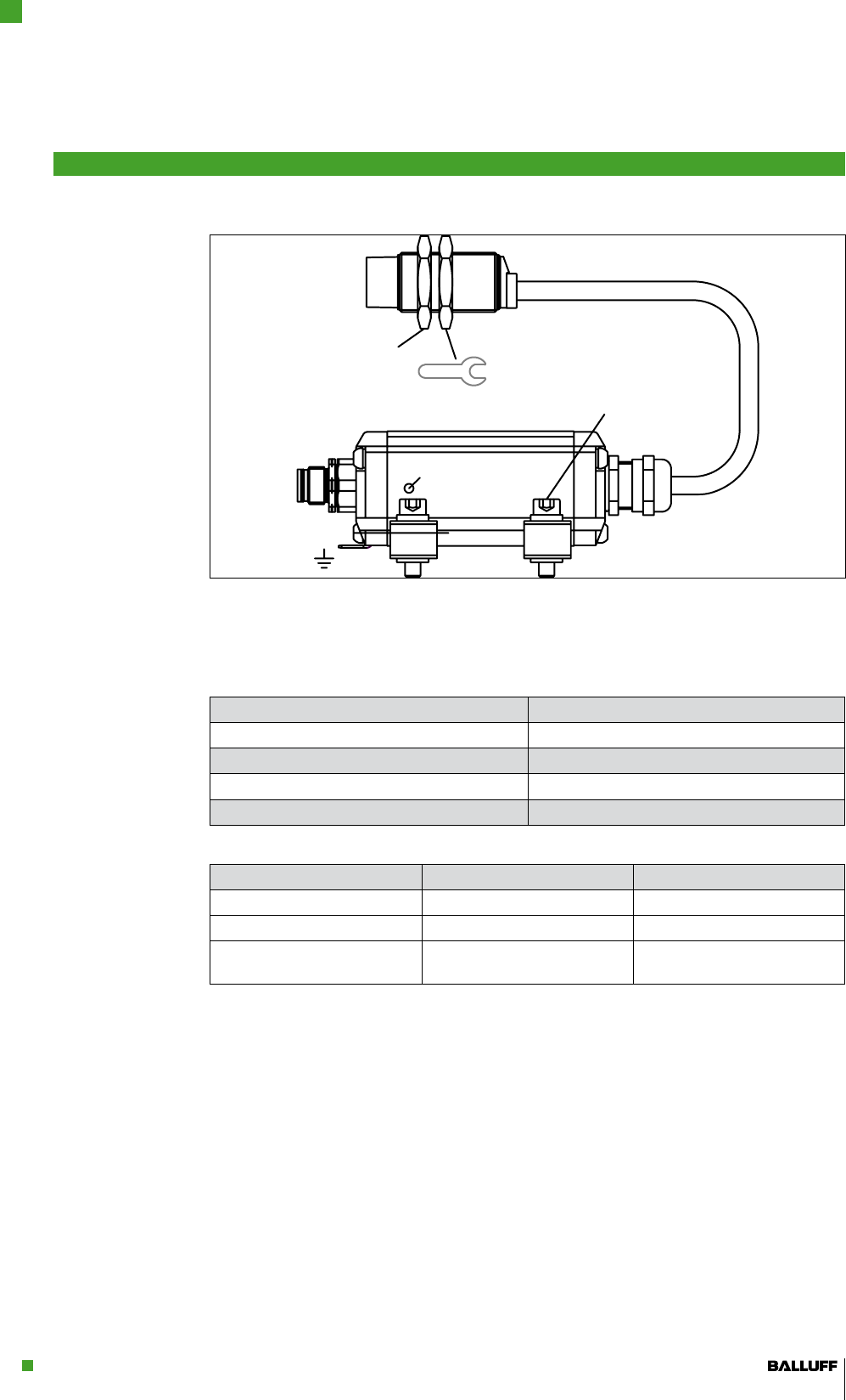
BIS M-400-045-001-07-S4 read/write deviceFig.9:
1 LED 2 Maximum tightening torque 40 Nm
Housing material Nickel-plated brass
Connection M12, 4-pin plug connection
Enclosure rating IP 67
Weight 100 g
BIS M-4xx IO-Link Device
Read/Write Device
www.balluff.com 17
LED Status Function
LED 1 Green Power
LED 1 Yellow Data carrier detected
LED 1 Green flashing
(1 s on / 100 ms off)
IO-Link connection active
BIS M-400-045-002-07-S4 read/write deviceFig.10:
1 LED 2 Maximum tightening torque 40 Nm
Housing material Nickel-plated brass
Wiring M12, 4-pin plug connection
Enclosure rating IP 67
Weight 100 g
LED Status Function
LED 1 and LED 2 Green Power
LED 1 and LED 2 Yellow Data carrier detected
LED 1 and LED 2 Green flashing
(1 s on / 100 ms off)
IO-Link connection active
$
/('
/('
/('
/('
$
LED
5.4 BIS M-400-045-
002-07-S4
Mechanical data
LED
Technical data
5
BIS M-4xx IO-Link Device
Read/Write Device
18
Technical data
5
5.5 BIS M-401-045-
001-07-S4
Mechanical data
LED
BIS M-401-045-001-07-S4 read/write deviceFig.11:
1 Maximum tightening torque 3 Nm 2 Earthing connector
3 Sensing surface
Housing material PBT
Connection M12, 4-pin plug connection
Enclosure rating IP 67
Weight 190 g
LED Status Function
LED 1 Green Power
LED 2 Yellow Data carrier detected
LED 1 Green flashing
(1 s on / 100 ms off)
IO-Link connection active
BIS M-4xx IO-Link Device
Read/Write Device
www.balluff.com 19
BIS M-402-045-002-07-S4 read/write device, values in mmFig.12:
1 Maximum tightening torque 25 Nm 2 Maximum tightening torque 2 Nm
3 LED
Housing material AlMGSIO5
Read/write head housing material Nickel-plated brass
Connection M12, 4-pin plug connection
Enclosure rating IP 67
Weight 220 g
LED Status Function
LED 1 Green Power
LED 1 Yellow Data carrier detected
LED 1 Green flashing
(1 s on / 100 ms off)
IO-Link connection active
5.6 BIS M-402-045-
002-07-S4
Mechanical data
LED
Technical data
5
BIS M-4xx IO-Link Device
Read/Write Device
20
BIS M-402-045-004-07-S4 read/write deviceFig.13:
1 Sensing surface 2 Maximum tightening torque 1 Nm
3 LED
Housing material AlMGSIO5
Read/write head housing material ABS-GF16
Connection M12, 4-pin plug connection
Enclosure rating IP 67
Weight 220 g
LED Status Function
LED 1 Green Power
LED 1 Yellow Data carrier detected
LED 1 Green flashing
(1 s on / 100 ms off)
IO-Link connection active.
5.7 BIS M-402-
045-004-07-S4
Mechanical data
LED
Technical data
5
BIS M-4xx IO-Link Device
Read/Write Device
www.balluff.com 21
BIS M-451-045-001-07-S4 read/write deviceFig.14:
1 Maximum tightening torque 3 Nm 2 Read/write axis
3 Earthing connector
Housing material PBT
Connection M12, 4-pin plug connection
Enclosure rating IP 67
Weight 360 g
LED Status Function
LED 1 Green Power
LED 2 Yellow Data carrier detected
LED 1 Green flashing
(1 s on / 100 ms off)
IO-Link connection active
5.8 BIS M-451-045-
001-07-S4
Mechanical data
LED
Technical data
5
BIS M-4xx IO-Link Device
Read/Write Device
22
The read/write device can read or write each individual byte on the data carrier. But since the
data carrier is divided into 16-byte memory blocks, the actual writing can only be performed in
blocks. Our processor electronics convert this time accordingly.
To calculate the read/write times, the block read or write time must, therefore, always be estima-
ted.
Data-carrier detection time
[mm]
Parameter "Used data carrier type“
All BIS M1xx-01 BIS M1xx-02
BIS M1xx-02 data carrier ≤ 40 - ≤ 27
BIS M1xx-01 data carrier ≤ 30 ≤ 18 -
Data carrier with 16 byte blocks BIS M-1xx-01 BIS M-1xx-02
First block to be read ≤ 20 ≤ 35
Other started 16 bytes ≤ 10 ≤ 25
Data carrier with 16 bytes per block BIS M-1xx-01 BIS M-1xx-02
First block to be read ≤ 40 ≤ 65
Other started 16 bytes ≤ 30 ≤ 55
Note
Fluctuations in the ms range are possible. Electrical noise effects may increase the
read/write time.
To calculate the permissible speed at which the data carrier and head may move relative to one
another, the static distance values are used (see Chapter 5 "Technical data“, pages 16 to 23).
The permissible speed is:
Vmax. perm..
Path 2 * |offset value|
= =
Time Processing time
The offset value is dependent on the read/write distance actually used in the system.
Processing time = Data-carrier
detection time +
Read/write time
of first block to
be read
+ n1X
Read/write time
for other started
blocks
1 Number of started blocks
Technical data
5
5.9 Dynamic mode
Memory access
Data carrier
detection time
Read times
Write times
Maximum speed
BIS M-4xx IO-Link Device
Read/Write Device

www.balluff.com 23
Technical data
5
Example
calculation
Note
The texts, such as "Read time of first block to be read", can also be represented as
variables: tL1.
Read and write 44 bytes starting with address 15 of a BIS M-102-01/L data carrier with
EEPROM memory and parameter setting of ALL for "Used data carrier type" using the BIS
M-400-045-001-07-S4 read/write device
The distance from the sensing surface of the read/write head to the data carrier is 12 mm. A
maximum clear zone is assumed, i.e. installation completely in plastic frame.
Address 15 is in block 1 (15/16 = 0.94 block 1)
Address 58 is in block 4 (58/16 = 3.63 block 4)
Therefore, a total of 4 blocks will be processed, where the first block always has a slightly longer
read or write time.
Calculation of read/write time:
Total read time = 30 ms + 20 ms + 3 x 10 ms = 80 ms
Total write time = 30 ms + 40 ms + 3 x 30 ms = 160 ms
For the specified values, this yields an offset of ± 20 mm.
Calculation of maximum speed:
Vmax.perm.read = 40 mm/80 ms = 0.5 m/s
Vmax.perm.write = 40 mm/160 ms = 0.25 m/s
Note
Fluctuations in the ms range are possible. Electrical noise effects may increase the
read/write time.
BIS M-4xx IO-Link Device
Read/Write Device
24
6.1 Digital point-to-
point connection
Three-conductor
physics
Communication
mode
Interleave mode
IO-Link integrates conventional and intelligent actuators and sensors into automation systems.
Mixed use of traditional and intelligent devices is possible with no additional expense.
IO-Link is intended as a communications standard below the traditional fieldbus level. Fieldbus-
neutral IO-Link transmission uses existing communications systems (fieldbuses or Ethernet-
based systems).
The actuators and sensors are connected in point-to-point connection using conventional
unshielded cables.
IO-Link devices can send application-specific parameters and data (e.g. diagnostics data) using
a serial communication procedure. Flexible telegrams are possible for sending larger quantities of
data. Communication is based on a standard UART protocol with 24V pulse modulation. Only
one data line is used for communication. This carries both the controller telegram as well as the
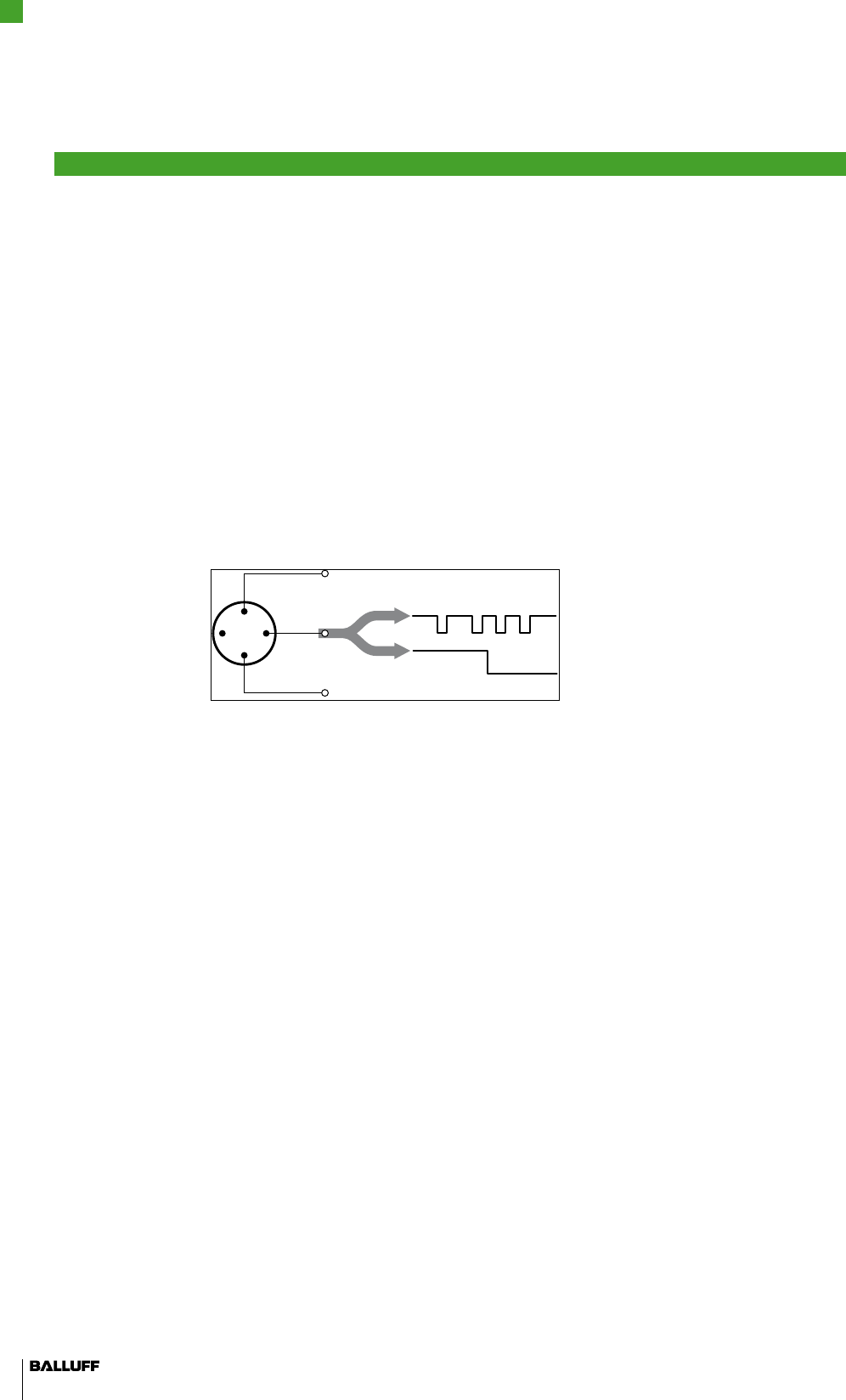
device telegram. This means that conventional 3-conductor physics is possible.
IO-Link supports both communication mode as well as standard IO mode (SIO). Standard IO
provides a switching signal on the communication line, as is used by normal binary switching
sensors. This mode is only possible with devices using 3-conductor connection technology.
Three-conductor physics of the IO-LinkFig.15:
The BIS M-4xx-045... supports both modes. In SIO mode, the "Data carrier in range" (24 V) or
"No data carrier in range" (0 V) signal is made available to the host system as a switching signal.
If the BIS M-4xx-045… is not used with an IO-Link Master and without triggering IO-Link com-
munication, it works in SIO mode and can be operated on a digital input.
The BIS M-4xx-045-... works in communication mode with Frame Type 1. In this transmission
type, 2 bytes of process data or required data are sent per frame (data block). This can take
place either from the IO-Link Master to the device or vice-versa.Process data are the application-
specific data; required data may contain parameters, service or diagnostic data.
So-called "Interleave Mode" makes it possible to send larger quantities of data. There, multiple
type 1 frames must be combined into a sequence. One frame with process data and one with
required data are sent in alternation.
With the BIS M-4xx-045-..., a sequence consists of 20 individual frames. 10 bytes of process
data are sent in each direction per sequence. This process data is described in greater detail in
Section 9.3 "Process data“ on page 32.
IO-Link basics
6
BIS M-4xx IO-Link Device
Read/Write Device

www.balluff.com 25
6.2 Process data
container
6.3 Identification
data and device
information
The IO-Link protocol provides a process data container 32 bytes in size. Addressing occurs in
the command byte, which is sent by the IO-Link Master. When process data is sent, addressing
is directly to the subindices 00hex … 1Fhex.
The BIS M-4xx-045-... processes 10 bytes of input and 10 bytes of output data (input
buffer/output buffer). The process data is mapped to the first 10 bytes of the process data
container (subindices 00hex…09hex).
IO-Link protocol
Subaddress
BIS M-4xx IO-Link device
Subaddress
00hex ⇒00hex
...
...
...
09hex ⇒09hex
0Ahex
...
1Fhex
Via the Service-PDu, in addition to the application-specific parameters, information stored on the
device can also be read.
SPDU Object name Length Information
Index Subindex
Identification data
0hex 8
9
10
11
12
Vendor ID 2 bytes Balluff Vendor ID = 0378hex
Device ID 3 bytes Balluff Device ID = 0602xxhex
10hex 0 Vendor name 7 bytes Balluff
11hex 0 Vendor text 15
bytes
www.balluff.com
12hex 0 Product name 23
bytes
Device designation
13hex 0 Product ID 7 bytes Order code
14hex 0 Product text 27
bytes
IO-Link RFID read-write
head
16hex 0 Hardware revision 5 bytes Hardware version
17hex 0 Firmware revision 5 bytes Firmware version
IO-Link basics
6
BIS M-4xx IO-Link Device
Read/Write Device

26
7.1 Required data The device-specific parameters of the Identification System can be parameterized via the SPDU.
The parameterization data of the BIS M-4xx-045-... is described in the following in greater detail.
Access Description Data
width
Value range Factory
setting
SPDU
Index Subindex
Parameterization data
40hex 1hex CRC yes/no 1 byte 0 = without CRC
1 = with CRC
0
40hex 2hex Dynamic mode
- yes/no
1 byte 0 = no
1 = yes
0
40hex 3hex Action if tag
present
1 byte 0 = no action
1 = serial number and tag type
7 = automatically read 8 bytes of data beginning at
a set start address after subindex 4 and 5
1
40hex 4hex Low byte of start
address for
autoread
2 bytes Observe data-carrier specifications. 0
40hex 5hex High byte of start
address for
autoread
40hex 6hex Used data-carrier
type
1 byte See Chapter 7.2 "Mapping of parameterization
data“, page 27
00hex=ALL
FEhex=BIS M1xx-01
FFhex=BIS M1xx-02
0
41hex 1hex Baud rate 1 byte 00hex = 4800 baud
01hex = 38400 baud
02hex = 230400 baud
1
Note
An entire index can be addressed via subindex 0 . For example, with index 40hex/
subindex 1hex, only the "CRCCheck" parameter is accessed. With index 40hex/subin-
dex 0, on the other hand, all parameters from "RCCheck" to "Used data carrier type"
can be addressed. The parameters are then arranged in byte blocks.
Parameterizing the read/write device
7
BIS M-4xx IO-Link Device
Read/Write Device
www.balluff.com 27
7.2 Mapping of
parameterization
data
CRC_16
Data check
Dynamic mode
To ensure data integrity, data transfer between the data carrier and read/write device can be
monitored using a CRC_16 data check.
With the CRC_16 data check, a checksum is written to the data carrier which enables the data
to be checked for validity at any time.
Advantages of the CRC_16 data check:
Very high data integrity, even during the non-active phase (data carrier outside the read/write –
head)
Restrictions of the CRC_16 data check:
Longer write times, as the CRC must also be written. –
User data capacity is sacrificed. – (see table on page 15).
Note
The CRC_16 data check can only be used in combination with data carriers that have
been appropriately initialized. If a data carrier is not initialized and this parameter is
nevertheless set, CRC errors occur during reading and writing (see Chapter 9.6 "Error
codes" page 43).
The data carriers can be initialized for using CRC16 with command designator 12 hex.
The checksum is written on the data carrier as 2 bytes (per block) of information. Thus, 2 bytes
of user data is lost per block.
The following figure applies for this parameter:
Index 40hex, subindex 1hex - 1 byte
7-MSB 6 5 4 3 2 1 0-LSB
not relevant 1/0*
* 0 = CRC_16 data check is not used (default setting).
1 = CRC_16 data check is used.
If dynamic mode is activated, a job can be sent even if no data carrier is located in the read/write
range of the read/write head, which would result in errors without dynamic mode. The job is then
stored and is executed as soon as a data carrier is detected.
The following figure applies for this parameter:
Index 40hex, subindex 2hex - 1 byte
7-MSB 6 5 4 3 2 1 0-LSB
not relevant 1/0*
* 0 = dynamic mode not activated (default setting).
1 = dynamic mode activated.
Parameterizing the read/write device
7
BIS M-4xx IO-Link Device
Read/Write Device
28
Action if tag
present
Start address for
autoread
Data carrier
Baud rate
The "Action on tag present" parameter specifies how the read/write device is to react if a new
data carrier is detected in the field. The default setting is to send the UID (serial number). In
addition, it is possible to set that nothing or a selected range of 8 bytes is to be sent immediately
as read data. The following values are permissible:
Index 40hex, subindex 3hex - 1 byte
0hex No action
1hex Send UID immediately
7hex Immediately send 8 bytes of data beginning at a set address
(parameter "Autoread start address“)
This parameter is only valid if "Autoread“ was selected as the action on tag present. The start
address can be set via subindices 4hex (low byte) and 5hex (high byte). The value range is depen-
dent on the specification of the data carrier; take this into account. An incorrect setting prevents
autoread from functioning; no data is output.
This parameter offers the possibility of specifying certain data carrier models that are to be
detected. All models, all BIS M1xx-01 models or all BIS M1xx-02 models can be selected. The
data carriers are detected more quickly if only those that are used are parameterized. The fol-
lowing values are permissible:
Index 40hex, subindex 6hex - 1 byte
0hex All data carrier models supported by Balluff
FEhex All BIS M1xx-01 model data carriers
FEhex All BIS M1xx-02 model data carriers
The Baud Rate parameter can be used to set the used transfer rate. The Min Cycle Time, i.e. the
time intervals at which the device may be queried by the IO-Link Master, is dependent on the
setting of this parameter. The following table applies:
Index 41hex, subindex 1hex - 1 byte
IO Link
designation
Baud Rate
[baud]
Parameter
setting
Min Cycle Time
COM1 4800 00hex 60hex = 12.8 ms
COM2 38400 01hex 35hex = 5.3 ms
COM3 230400 02hex 20hex = 3.2 ms
Note
Not all IO-Link Masters support COM3. This must absolutely be checked before
parameterizing! After the speed has been parameterized once, the device is only
parameterized for this speed and can only be reparameterized using a COM3-capa-
ble IO-Link Master. The Balluff-USB-Master is recommended for this purpose. Please
contact Balluff Sales for further information.
After saving the parameter, the M-4xx-045-... performs a reset. During this process,
IO Link communication is interrupted and errors can be displayed in the controller.
Only after this reset does the device restart with the newly set baud rate.
Parameterizing the read/write device
7
BIS M-4xx IO-Link Device
Read/Write Device

www.balluff.com 29
7.3 Storing the
parameterization
data
The set parameters are stored in the EEPROM memory of the BIS M-4xx-045-... On restart, the
most recently used parameters are used.
Note
Should it be necessary to exchange a BIS M-400-045-... in the system, make certain
that the correct parameter settings are programmed in the new device.
Parameterizing the read/write device
7
BIS M-4xx IO-Link Device
Read/Write Device

30
For information on starting up, please read the instructions for your IO-Link Master. BIS M4-xx
IO-Link devices use a process buffer of 10 bytes for both the input and the output.
Startup
8
BIS M-4xx IO-Link Device
Read/Write Device
www.balluff.com 31
9.1 Functional
principle
9.2 Functional
principle
The BIS M-4xx-045 Identification System is a contactless read and write system. The read/write
device consists of evaluation electronics with permanently connected read/write head.
The primary components of the BIS M-4xx-045 Identification System are:
Read/write device, –
Data carrier. –
Schematic representation of an Identification SystemFig.16:
1 Connection to the IO-Link Master 2 Read/write device
3 Data carriers 4 Read/write device
The data carrier is an autonomous unit which is supplied with power by the read/write head. The
read/write head continuously sends a carrier signal which is picked up by the data carrier from
within a certain distance. Once the data carrier is powered, a static read operation takes place.
The processor manages the data transfer between read/write head and data carrier, serves as a
buffer storage device, and sends the data to the controller.
The data is passed to the IO-Link Master using IO-Link protocol, and the Master then passes it
to the host system.
Host systems may be the following:
A control computer (e.g. industrial PC), –
A PLC. –
The BIS M-4xx-045 supports cyclical data exchange via IO-Link protocol and standard IO mode.
Detection of a data carrier (Codetag Present, 24 V) or no data carrier present (0 V) is sent on
data line C/Q as a digital switching signal.
With cyclical data exchange, read data from the BIS M-4xx-045 are cyclically exchanged with
the controller. It is also possible to read or enter parameter data in this operating mode.
Device function
9
BIS M-4xx IO-Link Device
Read/Write Device
32
9.3 Process data
Output/Input
buffer
Data exchange occurs via the process data, which, depending on the control system that is
used, is mapped in the input and output buffer or in a memory field. The BIS M-4xx-045 uses 10
bytes of input data and
10 bytes of output data; the assignments are described in the following. Subaddress 00hex
corresponds to the respective start address in the corresponding data field.
To transfer commands and data between the BIS M-4xx-045 read/write device and the host sys-
tem, the BIS M-4xx-045 provides two fields:
– Output buffer
– Input buffer
These fields are embedded in process data transmission via the IO-Link Master. As already
described, 10 bytes of process data are sent in each direction.
The mapping of this process data is described in the following:
Output buffer:
Bit-No.
Subaddress
76543210
00hex - 1st bit header TI KA GR AV
01hex Command designator or data
02hex Start address (low byte) or data
03hex Start address (high byte) or data
04hex Number of bytes (low byte) or data
05hex Number of bytes (high byte) or data
06hex Data
07hex Data
08hex Data
09hex - 2nd bit
header
TI KA GR AV
Explanations for output buffer:
Subaddress Bit
name
Meaning Function description
00hex 1st bit header
TI Toggle bit A state change during a job indicates that the
controller is ready to receive additional data made
available by the read/write device.
KA Head on/off 1 = Head off (read/write head switched off)
0 = Head on (read/write head in operation)
GR Ground state 1 = Software reset - causes the BIS to switch to
the ground state
0 = Normal operation
AV Job 1 = New job pending
0 = No new job or job no longer pending
Device function
9
BIS M-4xx IO-Link Device
Read/Write Device
www.balluff.com 33
Subaddress Bit
name
Meaning Function description
01hex Command
designator
00hex = No command
01hex = Read data carrier
02hex = Write data carrier
12hex = Initialize the CRC_16 data check on the
data carrier
32hex = Write a constant value on the data carrier
or data Data that is to be written on the data carrier
02hex Start address
Low byte
Low byte of the start address on the data carrier
for the current job
or data Data that is to be written on the data carrier
03hex Start address
High byte
High byte of the start address on the data carrier
for the current job
or data Data that is to be written on the data carrier
04hex No. of bytes
Low byte
Low byte of the data length for the current job
or data Data that is to be written on the data carrier
05hex No. of bytes
High byte
High byte of the data length for the current job
or data Data that is to be written on the data carrier
06hex Data Data that is to be written on the data carrier
07hex Data Data that is to be written on the data carrier
08hex Data Data that is to be written on the data carrier
09hex 2nd bit header
TI, KA,
GR, AV
If 1st and 2nd bit headers agree, valid commands
or data are present.
Note
To specify the start address and the number of bytes, the specifications of the used
data carrier and the maximum job size of 256 bytes are to be observed!
Device function
9
BIS M-4xx IO-Link Device
Read/Write Device
34
Input buffer:
Bit-No.
Subaddress
76543210
00hex - 1st bit header BB HF TO AF AE AA CP
01hex Error code or data or high-byte version
02hex Data or low-byte version
03hex Data
04hex Data
05hex Data
06hex Data
07hex Data
08he Data
09hex - 2nd bit
header
BB HF TO AF AE AA CP
Explanations for input buffer:
Subaddress Bit
name
Meaning Function description
00hex 1st bit header
BB Power 1 = Device is ready
0 = Device is in ground state
HF Head Failure 1 = Head is turned off
0 = Head is turned on
TO Toggle Bit A state change during a job indicates that the read/
write device is ready to transfer other data
AF Job Error 1 = Job incorrectly processed
0 = Job processed without errors
AE Job End 1 = Job processed without errors
0 = No job or job running
AA Job accepted 1 = The job was detected and accepted. Is being
processed.
0 = No job active
CP Codetag Present Data carrier is in the read range of the read/write
head
No data carrier in read range
Device function
9
BIS M-4xx IO-Link Device
Read/Write Device

www.balluff.com 35
Subaddress Bit
name
Meaning Function description
01hex Error code Error number is entered if the job was incorrectly
processed or canceled.
Only valid with AF bit!
00hex = No error
01hex = No data carrier in read/write range
02hex = Error during reading
03hex = Data carrier was removed from the read
range of
the head during reading
04hex = Error during writing
05hex = Data carrier was removed from the write
range of
the read/write head during writing.
07hex = AV-bit is set but command designator is
invalid or missing. Or: number of bytes is 00hex.
0Ehex = The CRC on the data carrier does not
agree with the calculated CRC for the read data.
0Fhex = 1st and 2nd bit header of the output buffer
do not agree.
20hex = Addressing of the job lies outside of the
memory range of the data carrier
21hex = Calls up a function that is not possible with
the current data carrier.
or data Data which was read from the data carrier
or SW version High byte of the software version
02hex Data Data which was read from the data carrier
or SW version Low byte of the software version
03hex Data Data which was read from the data carrier
04hex Data Data which was read from the data carrier
05hex Data Data which was read from the data carrier
06hex Data Data which was read from the data carrier
07hex Data Data which was read from the data carrier
08hex Data Data which was read from the data carrier
09hex 2nd bit header
BB, HF, TO, AF, AE, AA,
CP
If 1st and 2nd bit headers agree, there is valid data
present
Device function
9
BIS M-4xx IO-Link Device
Read/Write Device

36
Note
The 1st and 2nd headers must be compared by the user (host system) in order to
query the validity of the sent data.
When communication is initiated by the IO-Link Master, transmission of the current process data
begins.
As long as no data carrier was detected after start-up of the device, the firmware version of the
device is displayed in the first two user bytes (see Chapter 9.5 "Protocol examples“, page 37).
If a data carrier is detected, the "Reaction to Tag Present" set in the parameterization is execu-
ted. If, for example, display serial number is set here, the serial number of the currently detected
data carrier is displayed in index 01hex...08hex.
The bit headers of the output buffer can be used to control the device. For example, a device
restart can be triggered by setting the GR bit or a new job can be passed by setting the AV bit.
Furthermore, the write data can be passed to the device here.
The state of the device is displayed in the input buffer. Here, for example, the AF bit indicates an
error in the current job and the HF bit indicates that the head is currently switched off. In addi-
tion, the input buffer is used to pass read data and status codes. If no data carrier is present, the
most recent data is displayed in the input buffer. The deleted CP bit indicates that no data carrier
is in the field.
By means of this method, all functions of the read/write device can be used. This includes
reading, –
writing, –
dynamic reading, –
dynamic writing, –
writing a constant value, –
initializing CRC16 on the data carrier. –
Note
Note here that a job is limited to a maximum of 256 bytes. If more than 256 bytes are
to be processed, multiple, individual jobs must be started.
Functions can only be executed if a data carrier is in the read/write range. If a command is to be
sent that is not to be executed until the next tag is encountered, the device must be paramete-
rized for dynamic mode (see Chapter 7 "Parameterizing the read/write device“, page 26).
9.4 Protocol
sequence
Device function
9
BIS M-4xx IO-Link Device
Read/Write Device
www.balluff.com 37
The following examples show the protocol sequence in various situations.
Start the device, still no data in the output buffer:
Command from controller BIS M-4xx-045-... reaction
1. Process output buffer: 2. Process input buffer:
00hex GR, KA, AV = 0 00hex Set BB
09hex GR, KA, AV = 0 01hex e.g. 10hex = V 1.00
02hex e.g. 10hex
09hex Set BB
Reaction to Tag Present = no and new data carrier in the read range:
Command from controller BIS M-4xx-045-... reaction
1. Process output buffer: 2. Process input buffer:
00hex GR, KA, AV = 0 00hex Set CP
09hex GR, KA, AV = 0 09hex Set CP
Reaction to Tag Present = serial number and new data carrier in the read range:
Command from controller BIS M-4xx-045-... reaction
1. Process output buffer: 2. Process input buffer:
00hex GR, KA, AV = 0 00hex Set CP
09hex GR, KA, AV = 0 01 ... 08hex UID
09hex Set CP
Reaction to TagPresent = read (start address 5) and data carrier in the read range:
Command from controller BIS M-4xx-045-... reaction
1. Process output buffer: 2. Process input buffer:
00hex GR, KA, AV = 0 00hex Set CP
09hex GR, KA, AV = 0 01hex Address 5 read data
... Address 12 read data
01 ... 08hex UID
09hex Set CP
9.5 Protocol
examples
1st example
2nd example
3rd example
4th example
Device function
9
BIS M-4xx IO-Link Device
Read/Write Device
38
5th example
6th example
Device function
9
BIS M-4xx IO-Link Device
Read/Write Device
Data carrier no longer in detection range of the read/write head:
Command from controller BIS M-4xx-045-... reaction
1. Process output buffer: 2. Process input buffer:
00hex GR, KA, AV = 0 00hex Delete CP
09hex GR, KA, AV = 0 09hex Delete CP
Initialization of the CRC_16 data check on the data carrier (256 bytes beginning with
address 0):
Command from controller BIS M-4xx-045-... reaction
1. Process subaddresses in the order
shown:
2. Process input buffer:
01hex Command designator 12hex 00hex/09hex Set AA
02hex Start address 00hex
03hex Start address 00hex
04hex No. of bytes 00hex
05hex No. of bytes 01hex
00hex/09hex Set AV
3. Process subaddresses: 4. Copy received data, process subaddres-
ses of the input buffer:
01hex... 08hex Enter the first 8 bytes of data 00hex/09hex Invert TO
00hex... 07hex Invert TI
5. Process subaddresses: 6. Copy received data, process subaddres-
ses of the input buffer:
01hex... 08hex Enter the second 8 bytes of
data
00hex/09hex Invert TO
00hex... 09hex Invert TI
65. Process subaddresses: 66. Copy received data, process sub-
addresses of the input buffer:
01hex... 08hex Enter the last 8 bytes of data 00hex/09hex Set AE
00hex... 09hex Invert TI
67. Process subaddresses: 68. Process subaddresses:
00hex/09hex Delete AV 00hex/09hex Delete AA and AE
Note
Repeat the process with the new addresses until the entire memory range of the data
carrier is initialized.
www.balluff.com 39
7th example
Device function
9
BIS M-4xx IO-Link Device
Read/Write Device
Read 17 bytes starting at data carrier address 10:
Command from controller BIS M-4xx-045-... reaction
1. Process subaddresses in the order
shown:
2. Process input buffer:
01hex Command designator 01hex 00hex/09hex Set AA
02hex Start address 0Ahex 01hex... 08hex Enter the first 8 bytes of data
03hex Start address 00hex
04hex No. of bytes 11hex
05hex No. of bytes 00hex
00hex/09hex Set AV
3. Copy received data, process subaddres-
ses of the input buffer:
4. Process subaddresses of the input
buffer:
00hex... 09hex Invert TI 01hex... 08hex Enter second 8 bytes of data
00hex/09hex Invert TO
5. Copy received data, process subaddres-
ses of the input buffer:
6. Process subaddresses of the input
buffer:
00hex... 09hex Invert TI 01hex Enter last byte of data
02hex... 08hex 0x00 (empty)
00hex/09hex Invert TO, set AE
7. Copy received bytes, process sub-
addresses of the input buffer:
8. Process subaddresses of the input
buffer:
00hex... 09hex Delete AV 00hex/09hex Delete AF and AA
40
8th example Read 30 bytes starting at address 10 with read error:
Command from controller BIS M-4xx-045-... reaction
1. Process subaddresses in the order
shown:
2. Process input buffer:
01hex Command designator 01hex *Error occurred immediately*
02hex Start address 0Ahex 00hex/09hex Set AA
03hex Start address 00hex 01hex Enter error number
04hex No. of bytes 1Ehex 00hex/09hex Set AF
05hex No. of bytes 00hex
00hex/09hex Set AV
3. Evaluate error number and process
subaddresses of the output buffer:
4. Process subaddresses of the input
buffer:
00hex... 09hex Delete AV 00hex/09hex Delete AF and AA
Device function
9
BIS M-4xx IO-Link Device
Read/Write Device
www.balluff.com 41
9th example Write 18 bytes starting at data carrier address 20
Command from controller BIS M-4xx-045-... reaction
1. Process subaddresses in the order
shown:
2. Process input buffer:
01hex Command designator 02hex 00hex/09hex Set AA
02hex Start address 14hex
03hex Start address 00hex
04hex No. of bytes 12hex
05hex No. of bytes 00hex
00hex/09hex Set AV
3. Process subaddresses: 4. Copy received data, process subaddres-
ses of the input buffer:
01hex... 08hex Enter the first 8 bytes of data 00hex/09hex Invert TO
00hex... 07hex Invert TI
5. Process subaddresses: 6. Copy received data, process subaddres-
ses of the input buffer:
01hex... 08hex Enter the second 8 bytes of
data
00hex/09hex Invert TO
00hex... 09hex Invert TI
7. Process subaddresses: 8. Copy received data, process subaddres-
ses of the input buffer:
01hex... 02hex Enter the remaining 2 bytes of
data
00hex/09hex Set AE
00hex... 09hex Invert TI
9. Process subaddresses: 10. Process subaddresses:
00hex/09hex Delete AV 00hex/09hex Delete AA and AE
Device function
9
BIS M-4xx IO-Link Device
Read/Write Device
42
10th
example
11th
example
12th
example
Write constant data. 20 bytes, value 5Ahex, starting at address 0:
Command from controller BIS M-4xx-045-... reaction
1. Process subaddresses in the order
shown:
2. Process input buffer:
01hex Command designator 32hex 00hex/09hex Set AA
02hex Start address 00hex
03hex Start address 00hex
04hex No. of bytes 14hex
05hex No. of bytes 00hex
06hex Value 5Ahex
00hex/09hex Set AV
3. Data is written
00hex/09hex Set AE
4. Process subaddresses: 5. Process subaddresses:
00hex/09hex Delete AV 00hex/09hex Delete AA and AE
Move read/write device to ground state:
Command from controller BIS M-4xx-045-... reaction
1. Process subaddresses: 2. Process input buffer:
00hex/09hex Set GR 01...08hex 00hex (empty)
00hex/09hex Delete BB
3. Process subaddresses: 4. Process input buffer:
00hex/09hex Delete GR 00hex/09hex Set BB
Perform head shutdown:
Command from controller BIS M-4xx-045-... reaction
1. Process subaddresses: 2. Process input buffer:
00hex/09hex Set KA 00hex/09hex Set HF, delete CP
New data carriers are not detected,
antenna is shut down.
3. Process subaddresses: 4. Process input buffer:
00hex/09hex Delete KA 00hex/09hex Set HF
New data carriers are now detected
again.
Device function
9
BIS M-4xx IO-Link Device
Read/Write Device

www.balluff.com 43
9.6 Error codes Error
code
Meaning Remedy
01hex No data carrier in read/write range Data carriers must already be in the
read/write range when a command is
sent; otherwise dynamic mode must be
parameterized.
02hex Read error Repeat job.
03hex Data carrier was removed from the read
range of the head during reading.
04hex Write error Repeat job.
05hex Data carrier was removed from the write
range of the read/write head during
writing.
07hex AV is set, but the command designator is
invalid or missing. Or: number of bytes is
00hex.
Please check and correct.
0Ehex CRC error Data carrier was not successfully read.
Possible causes:
Data carrier defective –
Transmission failed –
Data carrier not CRC capable –
0Fhex Bit header error The two headers in the output buffer and
in the host system do not agree.
The headers must be matched (see
"Output buffer“,
page 32).
20hex Addressing of the job lies outside of the
memory range of the data carrier.
Please correct addressing, taking into
account the used data carrier.
21hex Calls up a function that is not possible
with the current data carrier.
Observe permissible commands for the
current data carrier.
Note
If an error occurs, a new command cannot be executed until the AV has first been
deleted, i.e. the faulty job has been completed in full.
Device function
9
BIS M-4xx IO-Link Device
Read/Write Device
44
9.7 Data
transmission
timing
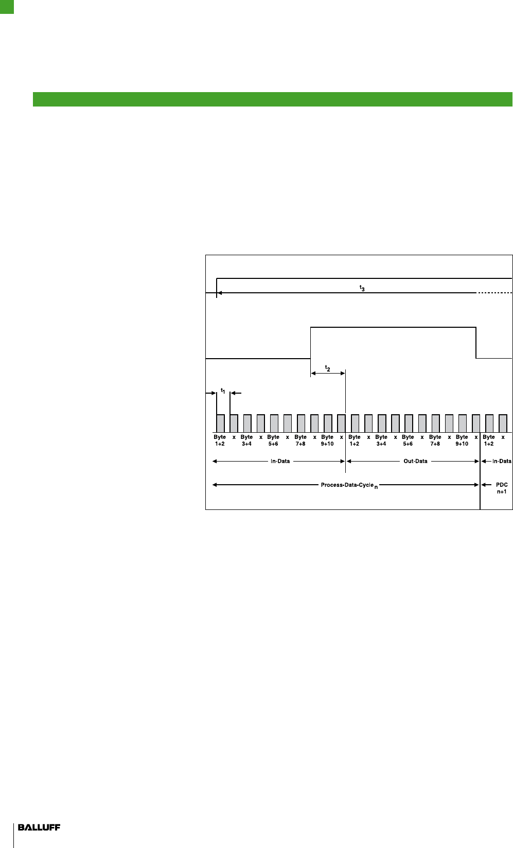
The sequence of the IO-Link communication is shown in the following diagram. Exchange alter-
nates between the input buffer and the output buffer. As soon as current data is pending in one
of the buffers, it is exchanged on the next in or out data cycle. The problem arises here that the
transmission times can vary greatly. If data is updated shortly before the start of the respective
exchange cycle, the transfer lasts just over 10 x cycle time (e.g. t2). If, however, data is updated
shortly after the start of an exchange cycle, it lasts a maximum of 3 x 10 x cycle time (e.g. t3).
The processing sequence of a command is shown on the next page using a read job of 9…16
bytes (2 x input buffer for read data) as an example.
IO-Link transmission sequenceFig.17:
t1 Cycle time In-Data: Input data
t2 Polling time Out-Data: Output data
t3 Cycle time Process Data Cycle: Process data cycle
Byte a+b: Process data
x: Required data
Cycle time t1:
Time until the data of a data carrier that enters the read range is read. The read time is 70 ms x
number of parameterized data comparison counts, default = 2 (see Chapter 7.2 "Mapping of
parameterization data“, page 27).
Polling time t2:
Time until it is recognized that the data carrier is no longer in the read range (polling time). The
polling time is xx ms.
Cycle time t3:
Time between the sending of two frames. The cycle time is dependent on the set baud rate and
on the respective Master.
Device function
9
BIS M-4xx IO-Link Device
Read/Write Device
www.balluff.com 45
In-Data/Out-Data:
Sending of the input data and output data. 10 frames of 2 bytes each are sent, alternating
between process data and required data (x).
Process Data Cycle:
A process data cycle consists of the complete sending of the input and output data. At the
beginning of each process data cycle, the current data are polled and immediately sent.
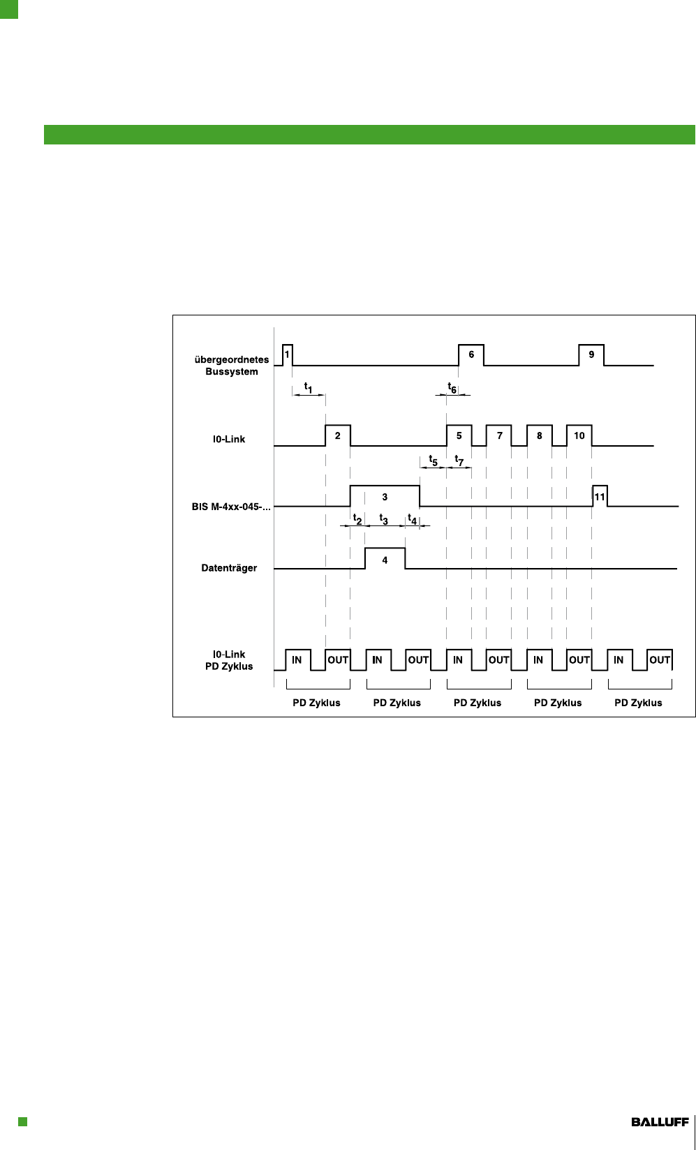
IO-Link transmission sequenceFig.18:
1 The command is passed on to the IO-Link Master by the controller via a bus system.
2 After the synchronization time t1, the command is passed on to the BIS M-400-045-… via IO-Link. The
duration is dependent on the bus system, the Master, the cycle time and the current state of the IO-
Link communication (see problem described above).
3 The processing time begins with the arrival of the command at the M-400-045-…This is composed of
the time for the command processing t2, the time for the actual read operation t3 and the evaluation
time for the read data t4. A flat value of max. 3 ms can be estimated for t2 and t3. The pure read time is
calculated as described (see Chapter 5.9 "Dynamic mode", page 22). Please note: If the data carrier that
is to be read was already detected by the device, the time for data carrier detection is eliminated.
4 The pure time for data carrier processing is shown here.
5 Following another synchronization time t5, the first data is passed on to the IO-Link Master with the next
In-Data cycle. In addition, the AE-bit is set in the bit header. The time for this is t7 = 10 x cycle time.
6 The data is only passed on to the controller via the host bus system. The latency period t6 is dependent
on the bus system and the IO-Link Master.
7 After the first data arrives at the controller, the toggle-bit in the output buffer must be inverted (see
Chapter 9 "Device function“, page 31). In the example, it is assumed that the this occurs immediately
and that the transfer to the IO-Link Master happens fast enough that the BIS M-400-045-… receives the
new data on the next Out-Data cycle.
Device function
9
BIS M-4xx IO-Link Device
Read/Write Device

46
8 Now, the device places the next and, thus, the last bytes of the read data in the input buffer and inverts
the toggle bit.
9 The controller retrieves the data and deletes the AV bit.
10 The re-updated output buffer is sent to the BIS M-400-045-….
11 The device ends the read command and deletes the bits in the bit header in the input buffer that belong
to the job .
Note
The sequence for a write command occurs analogously. Here, the data is transfered
via IO-Link and the actual writing on the data carrier is interchanged.
A maximum command processing time can be approximated as follows:
Ttotproc.max = 40 x tcyc + read/write speed + 5 ms + 30 x tcyc + 20 x tcyc x n1 =
5 ms + tread/write speed2 + tcyc3 x (70 + 20 x n)
1 Number of bytes/8 (rounded to the next whole number)
2 Calculated time for data carrier processing (see Chapter 5.9 "Dynamic mode“, page 22)
3 Master Cycle Time.
Note
The actual required time may be considerably less than the maximum processing
duration.
Note
Prerequisite for calculating the maximum command processing time is that no delays
occur in the host bus system and in the controller.
Device function
9
BIS M-4xx IO-Link Device
Read/Write Device

www.balluff.com 47
Type designation
code
Accessories
(optional, not
included)
Appendix
BIS M-4xx IO-Link Device
Read/Write Device
BIS M – 4xx – 045 – 0xx –07– S4
Balluff Identification System
Series
M = Read and write system, 13.56 MHz
Hardware type
4xx = Read/write device
Software type
045 = Software number, IO-Link
Version
001 = Standard
002 = Tapered
interface
0 7 = IO-Link
module
S4 = M12 4-pin male
Accessories for the BIS M-4xx-... can be found in the Balluff IO-Link catalog.
The catalog can be downloaded on the Internet at "www.balluff.de".

48
Decimal Hex Control
code
ASCII Decimal Hex ASCII Decimal Hex ASCII
0 00 Ctrl @ NUL 43 2B + 86 56 V
1 01 Ctrl A SOH 44 2C , 87 57 W
2 02 Ctrl B STX 45 2D - 88 58 X
3 03 Ctrl C ETX 46 2E . 89 59 Y
4 04 Ctrl D EOT 47 2F / 90 5 A Z
5 05 Ctrl E ENQ 48 30 0 91 5B [
6 06 Ctrl F ACK 49 31 1 92 5C \
7 07 Ctrl G BEL 50 32 2 93 5D [
8 08 Ctrl H BS 51 33 3 94 5E ^
9 09 Ctrl I HT 52 34 4 95 5F _
10 0 A Ctrl J LF 53 35 5 96 60 `
11 0B Ctrl K VT 54 36 6 97 61 A
12 0C Ctrl L FF 55 37 7 98 62 B
13 0D Ctrl M CR 56 38 8 99 63 c
14 0E Ctrl N SO 57 39 9 100 64 d
15 0F Ctrl O SI 58 3 A : 101 65 e
16 10 Ctrl P DLE 59 3B ; 102 66 f
17 11 Ctrl Q DC1 60 3C < 103 67 g
18 12 Ctrl R DC2 61 3D = 104 68 h
19 13 Ctrl S DC3 62 3E > 105 69 i
20 14 Ctrl T DC4 63 3F ? 106 6 A j
21 15 Ctrl U NAK 64 40 @ 107 6B k
22 16 Ctrl V SYN 65 41 A 108 6C L
23 17 Ctrl W ETB 66 42 B 109 6D m
24 18 Ctrl X CAN 67 43 C 110 6E n
25 19 Ctrl Y EM 68 44 D 111 6F o
26 1 A Ctrl Z SUB 69 45 E 112 70 p
27 1B Ctrl [ ESC 70 46 F 113 71 q
28 1C Ctrl \ FS 71 47 G 114 72 r
29 1D Ctrl ] GS 72 48 H 115 73 s
30 1E Ctrl ^ RS 73 49 I 116 74 t
31 1F Ctrl _ US 74 4 A J 117 75 u
32 20 SP 75 4B K 118 76 V
33 21 ! 76 4C L 119 77 W
34 22 " 77 4D M 120 78 X
35 23 # 78 4E N 121 79 Y
36 24 $ 79 4F O 122 7 A Z
37 25 % 80 50 P 123 7B {
38 26 & 81 51 Q 124 7C |
39 27 ‘ 82 52 R 125 7D }
40 28 ( 83 53 S 126 7E ~
41 29 ) 84 54 T 127 7F DEL
42 2 A * 85 55 U
ASCII table
Appendix
BIS M-4xx IO-Link Device
Read/Write Device

www.balluff.com 49
A
Dimensions 16, 18, 19, 21, 22
Distance
between the data carriers 11
between the read/write devices 11
Sensing surface 8, 9, 10, 16, 17, 18, 20
ASCII table 48
Output buffer 25, 32, 37, 43, 44, 45, 46
B
Baud rate 26, 28, 44
Intended use 7
Operating conditions 16
C
CRC check
Error message 31
D
Data carrier
ISO 15693 15, 26
Mifare 15, 22, 26
Data transfer 12, 14, 27, 31
Data transmission 12
E
Input buffer 14, 25, 32, 34, 36, 38, 39,
40, 41, 42, 44, 46
Electrical data 17
Ground 11
Earthing connector 9, 10, 18, 21
F
Clear zone 23
Function indicators 20
Functional principle 12
I
Startup 5, 7
Installation 5, 7
K
Cable length 9, 10, 19, 20
Characteristic data in combination with
data carriers 22, 23
Communications standard 5, 24
L
Read distance 11, 14, 22
M
Mechanical data 16, 17, 18, 19, 20, 21
P
Protocol examples 36
Process data 14, 15, 24, 25, 32, 36,
44, 45
S
Safety 7
Operation 7
Startup 7
Installation 7
Safety regulations 7
T
Technical data
Operating conditions 16
Electrical data 17
Function indicators 20
Characteristic data in combination
with data carriers 22, 23
Mechanical data 16, 17, 18, 19, 20,
21
Type designation code 47
Z
Accessories 47
Appendix
BIS M-4xx IO-Link Device
Read/Write Device

Balluff GmbH
Schurwaldstraße 9
73765 Neuhausen a.d.F.
Germany
Tel. +49 7158 173-0
Fax +49 7158 5010
balluff@balluff.de
No. 870554 E . Edition 1005; Subject to modifications.
www.balluff.com
www.balluff.com