Bang and Olufsen a s CR870-2Q JukeBlox Networked Media User Manual dat CR860 CR870 3 6 datasheet
Bang & Olufsen a/s JukeBlox Networked Media dat CR860 CR870 3 6 datasheet
Contents
- 1. user manual
- 2. Revised user manual
user manual
Data Sheet: CR Series
JukeBlox Networked Media Modules
dat_CR860_CR870_3_6_datasheet.doc CONFIDENTIAL Version 3.6 – August 4th 2011 - Page 1 of 26
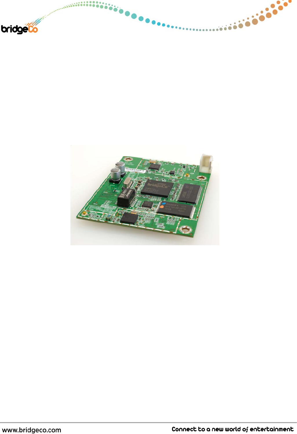
JukeBlox Networked Media Module
CR Series
Datasheet
Complete audio networking system on a small module
Integrated Ethernet + USB2.0
WiFi-certified 802.11b/g
Built-in PIFA antenna
Glueless audio, video and control ports
FCC certified
Ideal for enabling network and USB audio playback for iPod
docks, audio systems, AV Receivers, active speaker systems,
internet radios, network playback adaptors
CONFIDENTIAL

Data Sheet: CR Series
JukeBlox Networked Media Modules
dat_CR860_CR870_3_6_datasheet.doc CONFIDENTIAL Version 3.6 – August 4th 2011 - Page 2 of 26
Table of Contents
1. Introduction 4
2. Block Diagram 4
3. Board Pictures 5
3.1 Top View of CR870-2A 5
3.2 Bottom View of CR870 types 2A, 2D & 2S 5
3.3 Top View of CR870 types 2C, 2F, 2G, 2I, 2J, 2K & 2R 6
3.4 Bottom View of CR870 types 2C, 2G, 2I, 2J, 2K, 2L, 2N, 2O, 2P & 2R 6
3.5 Top View of CR870 types 2D, 2L, 2N, 2O, 2P, 2Q & 2S 7
4. Ordering Guide 8
5. Electrical Specifications 9
5.1 Absolute Maximum Ratings 9
5.2 Operating Conditions 10
5.3 WiFi Specification (CR870 only) 10
6. Regulatory Compliance and Quality 11
6.1 RoHS 12
6.2 Environmental Test 12
6.3 ESD and Transient Test (Applies to LAN and USB external connections only) 12
6.4 Magnetic Field Test 12
6.5 MTBF 12
6.6 Mechanical Specifications 12

Data Sheet: CR Series
JukeBlox Networked Media Modules
dat_CR860_CR870_3_6_datasheet.doc CONFIDENTIAL Version 3.6 – August 4th 2011 - Page 3 of 26
6.7 Module Quality 12
7. Board Dimensions and Weight 13
7.1 Top View and Side View of CR870 modules with PIFA antenna & no shields 13
7.2 Bottom View of CR870 modules with no bottom shield 13
7.3 Top View and Side View of CR870 modules without PIFA antenna 14
7.4 Top View and Side View of CR870 modules with PIFA antenna & top shield 14
7.5 Module weight 15
8. Connectors and Connections 15
8.1 WLAN UFL Antenna Connector (optional) 15
8.1.1 Coaxial antenna connector dimensions 15
8.2 Module Connectors 15
8.2.1 Pin Descriptions 16
8.2.2 Connector PIN Assignments 20
9. Application Guidelines 21
9.1 Power Supply sequencing and Reset Timing 21
9.1.1 Power up, Reset and Power Down Timing 22
9.2 RF Considerations 22
10. Revision Control 23
Module Revision History 26
Trademarks 26
Warranty Limitations 26
Data Sheet: CR Series
JukeBlox Networked Media Modules
dat_CR860_CR870_3_6_datasheet.doc CONFIDENTIAL Version 3.6 – August 4th 2011 - Page 4 of 26
1. Introduction
The CR-series module is a single-board networked media player module, based on BridgeCo’s DM860
and DM870 media processors, and enables fast product developments with Ethernet, USB and
optional WiFi connectivity. The module connects to standard legacy components in various audio,
video/LCD and control formats.
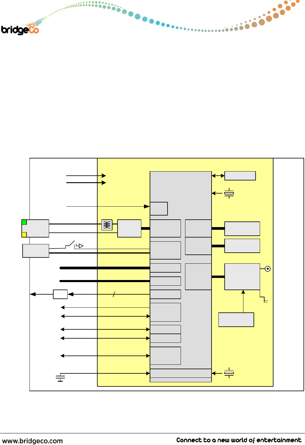
2. Block Diagram
Ethernet
PHY
DM860
or
DM870
256 Mbit
SDRAM
JTAG
RJ-45
100B-T
Mem
USB
GPIO
24.000 MHz
Reset In
NAND 1 GB
NAND flash
802.11
RF amp
(optional)
802.11
RMII
SPI
RTC 32.768 kHz
USB
(Host)
USB
RST
UART
5V
3.3V
JukeBlox Networked Media Module – CR Series
1.2V
Stereo Out
Video Out
Audio I/O
4/8bit MMC
3x6bit RGB
2 x UART
SPI Ctrl.
max. 20 GPIOs
3.3V (RTC)
SuperCap
IR sensor
reset signals
analog mute
I2C bus
shift register
IC control
serial control
A/D, D/A
S/PDIF
CCIR-656
LP 2
HP out
Display
SD-Card
AV
Ports
LCD
SSM
DAC
PIFA
Antenna
Switcher
1.9V
Data Sheet: CR Series
JukeBlox Networked Media Modules
dat_CR860_CR870_3_6_datasheet.doc CONFIDENTIAL Version 3.6 – August 4th 2011 - Page 5 of 26
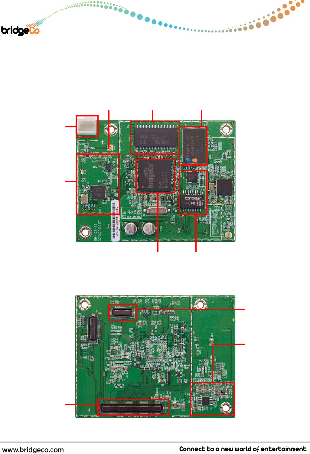
3. Board Pictures
3.1 Top View of CR870-2A
3.2 Bottom View of CR870 types 2A, 2D & 2S
PIFA
antenna
802.11b/g
front-end
BridgeCo
p
rocessor
Ethernet
FLASH
SDRAM
antenna
connector
Media
connector
LCD
connector
Note: Components and
Socket to the right of the
Ethernet and Flash
sections are not installed
in production modules.
Please see Section 3.3
for example production
module top view picture.
Note: The connector
shown to the left of the
LCD connector is not
installed on production
modules. Please see
section 3.4 for example
production module
bottom view picture.
+1.9V DC to DC
converter
Data Sheet: CR Series
JukeBlox Networked Media Modules
dat_CR860_CR870_3_6_datasheet.doc CONFIDENTIAL Version 3.6 – August 4th 2011 - Page 6 of 26
3.3 Top View of CR870 types 2C, 2F, 2G, 2I, 2J, 2K & 2R
3.4 Bottom View of CR870 types 2C, 2G, 2I, 2J, 2K, 2L, 2N, 2O, 2P & 2R
Versions with no bottom
shield and no LCD
connector.
Please note that
production version does
not have exposed solder
on the underside of the
mounting holes.
Version with no top
shield.
Please note that label
text will change to show
version, and versions 2I,
2J, 2K will have no
Ethernet components
mounted.
Data Sheet: CR Series
JukeBlox Networked Media Modules
dat_CR860_CR870_3_6_datasheet.doc CONFIDENTIAL Version 3.6 – August 4th 2011 - Page 7 of 26
3.5 Top View of CR870 types 2D, 2L, 2N, 2O, 2P, 2Q & 2S
Versions with top shield.
For versions without PIFA
antenna, PIFA antenna is
not present and UFL
connector is present, see
the top view of CR870-2A
for location of UFL
connector.
Data Sheet: CR Series
JukeBlox Networked Media Modules
dat_CR860_CR870_3_6_datasheet.doc CONFIDENTIAL Version 3.6 – August 4th 2011 - Page 8 of 26
4. Ordering Guide
Part
Number BridgeCo ICs
WiFi Ethernet USB Real-
Time
Clock LCD PIFA
Antenna
Ext.
Antenna
UFL Conn. SDRAM Top Module
Shielding
Contains
shield
Incl.
connector
CR870-2A DM870+T6201 X X X X X X (X)* 32MB
CR870-2C DM870+T6201 X X X X 32MB
CR870-2D DM870+T6201 X X X X X 32MB X
CR870-2F DM870+T6201 X X X X X X (X)* 32MB
CR870-2G DM870+T6201 X X X X 32MB
CR870-2I DM870+T6201 X X X 16MB
CR870-2J DM870+T6201 X X X X 16MB
CR870-2K DM870+T6201 X X X X 16MB
CR870-2L DM870+T6201 X X X X 32MB X
CR870-2M DM870+T6201 X X X X X X (X)* 32MB X
CR870-2N DM870+T6201 X X X 16MB X
CR870-2O DM870+T6201 X X X X 16MB X
CR870-2P DM870+T6201 X X X X 32MB X
CR870-2Q DM870+T6201 X X X X 32MB X
CR870-2R DM870+T6201 X X X X 16MB
CR870-2S DM870+T6201 X X X X X 32MB X
CR860-2A DM860 n/a X X n/a n/a 32MB
CR860-2B DM860 n/a X X X X n/a n/a 32MB
* Connector on board, but not enabled
Note: Shaded rows are Custom or Obsolete configurations – not to be used for new /
standard MP designs.
Data Sheet: CR Series
JukeBlox Networked Media Modules
dat_CR860_CR870_3_6_datasheet.doc CONFIDENTIAL Version 3.6 – August 4th 2011 - Page 9 of 26
5. Electrical Specifications
Parameter State Model Voltage Symbol min. typ. max. Units
Power Supply Voltage VIN +2.97
+1.08 +3.3
+1.2 +3.63
+1.32 V
V
Logic Input high voltage VIH 1.7 5.5 V
Logic Input low voltage VIL -0.3 0.7 V
Logic Input threshold voltage VIT 1.29 1.39 1.5 V
Schmitt-trigger input low to
high threshold voltage VIT+ 1.58 1.65 1.71 V
Schmitt-trigger input high to
low threshold voltage VIT- 0.95 1.01 1.06 V
Logic Output high voltage VOH 2.4 V
Logic Output low voltage VOL 0.4 V
Logic Low-level output current
(VOL=0.4V) IOL -9.6 -15.6 -19.3 mA
Logic High-level output current
(VOH=2.4V) IOH 11.1 22.5 35.3 mA
3.3V PIN3.3 - 230 300 mW CR870
int 1.9V 1.2V PIN1.2 - 45 60 mW
3.3V PIN3.3 - 165 215 mW
1.2V PIN1.2 - 45 60 mW
CR870
ext 1.9V 1.9V PIN1.9 - 35 50 mW
3.3V PIN3.3 - 145 190 mW
Reset
State
CR860 1.2V PIN1.2 - 45 60 mW
3.3V PIN3.3 - 1750 2275 mW CR870
int 1.9V 1.2V PIN1.2 - 600 800 mW
3.3V PIN3.3 - 825 1075 mW
1.2V PIN1.2 - 600 800 mW
WLAN
Operating
CR870
ext 1.9V 1.9V PIN1.9 - 535 700 mW
3.3V PIN3.3 - 760 990 mW
Power Consumption
Operating CR860 1.2V PIN1.2 - 600 800 mW
Note: The maximum power consumption values are 30% larger than the typical values.
The maximum values are intended to be used for power supply sizing calculations.
5.1 Absolute Maximum Ratings
Parameter Component Min Max Units
3.3V Supply Voltage -0.5 4.6 V
1.2V Supply Voltage -0.5 1.8 V
Logic Input Voltage -0.5 6 V
Logic Output Voltage
Main
-0.5 4.6 V
Data Sheet: CR Series
JukeBlox Networked Media Modules
dat_CR860_CR870_3_6_datasheet.doc CONFIDENTIAL Version 3.6 – August 4th 2011 - Page 10 of 26
5.2 Operating Conditions
Parameter Min Max Units
Operating Temperature 0 +70 °C
Operating Humidity 10 90 (non condensing) %RH
Storage Temperature -10 +75 °C
Storage Humidity 10 95 (non condensing) %RH
Storage Temperature Cycle Test 24 hrs -10 +75 °C
5.3 WiFi Specification (CR870 only)
Feature Description
WLAN Standards IEEE 802.11b
IEEE 802.11g
Frequency Band 2.412 – 2.472 GHz (2.4GHz ISM Band, 13 Channels)
Channel 1 - Channel 13
North America, Japan Telec, Europe ETSI
Modulation 802.11b mode (DS-SS: IEEE 802.11b)
802.11g mode (OFDM: IEEE 802.11g)
Transmission Speed 802.11b mode
11Mbps, 5.5Mbps, 1Mbps
802.11g mode
54Mbps, 48Mbps, 36Mbps, 24Mbps, 18Mbps, 12Mbps, 9Mbps, 6Mbps
Tx Power 802.11b mode (16.5dBm, +/-1dBm)
802.11g mode (21dBm, +/-1dBm)
Power-on Ramp < 2us
RF Carrier Suppression < 15dBc
TX EVM < -9dB @ 6Mbps
< -25dB @ 54Mbps
Rx Sensitivity
(incl. CE2 Mother board) 802.11b mode
=<-88dBm @ 1Mbps, =<-85dBm @ 5.5Mbps, =<-83dBm @ 11Mbps
802.11g mode
=<-86dBm @ 6Mbps, =<-75dBm @ 36Mbps, =<-69dBm @ 54Mbps
Throughput Rate
(measured for each
module)
See factory test specification
Data Sheet: CR Series
JukeBlox Networked Media Modules
dat_CR860_CR870_3_6_datasheet.doc CONFIDENTIAL Version 3.6 – August 4th 2011 - Page 11 of 26
6. Regulatory Compliance and Quality
Description Country Compliance Module Versions Passed
Electromagnetic Compatibility
(Prescan) USA
Europe FCC CFR47 Part15B
EN 55022
EN 55024
EN 61000-3-2
EN 61000-3-3
EN 61000-4-2
EN 61000-4-3
EN 61000-4-4
EN 61000-4-5
EN 61000-4-6
EN 61000-4-8
EN 61000-4-11
Radio Regulations (CR870
only) USA
Japan
Canada
Europe
New Zealand/Australia
China
Korea
FCC Part 15C
Telec
IC RSS-210
CE
CE
SRRC
KCC
C, G, I, J, D
C, G, J, D
C, G, I, J, D
C, G, J
Note: BridgeCo does not certify all module variants for all countries.
Please contact your BridgeCo sales office for the latest information about which modules
are certified for which countries, and arranging for additional certification for
your chosen module if needed. Product manufacturers are responsible for the end
product certification.
Several products using CR870 series modules have passed the WiFi Alliance logo
certification tests. BridgeCo can help manufacturers to prepare for the WiFi Alliance tests
by providing an example test plan and the required commands to enable special test
modes. Please contact your BridgeCo sales office about WiFi Alliance logo certification
assistance.

Data Sheet: CR Series
JukeBlox Networked Media Modules
dat_CR860_CR870_3_6_datasheet.doc CONFIDENTIAL Version 3.6 – August 4th 2011 - Page 12 of 26
6.1 RoHS
Uses only RoHS compliant components
6.2 Environmental Test
Withstands 4 hours at 70°C, 90% RH
6.3 ESD and Transient Test (Applies to LAN and USB external connections
only)
ESD: +/- 2kV operation, +/- 4kV no destruction (part of CE test)
Fast electrical transients: +/- 500V operation, +/- 1000V no destruction (part of CE test)
6.4 Magnetic Field Test
Passes EN55022 and EN55024 (part of CE test)
6.5 MTBF
>10000 hours
6.6 Mechanical Specifications
Passes drop test according to I.E.C. 68-2-32, height 100 cm, 1 corner, 6 faces.
Passes vibration test with sine, vertical, 60 minutes, 600 to 18000 cpm, 1G
6.7 Module Quality
Defect Rate: 7 months <0.5% failures, 14 months <1% failures
AQL CR=0, MA=0.4, MI=0.4
Data Sheet: CR Series
JukeBlox Networked Media Modules
dat_CR860_CR870_3_6_datasheet.doc CONFIDENTIAL Version 3.6 – August 4th 2011 - Page 13 of 26
7. Board Dimensions and Weight
Note: For mechanical details of versions CR870-2C Mfg200 and CR870-2Q, please see the appropriate addendum:
dat_CR860_CR870_3_3_datasheet_addendum_2C_Mfg200a.pdf or dat_CR860_CR870_3_5_datasheet_addendum_2Q.pdf.
These addendums are available upon request from BridgeCo.
7.1 Top View and Side View of CR870 modules with PIFA antenna & no
shields
7.2 Bottom View of CR870 modules with no bottom shield
Note:
1. All dimensions are measured in millimetres (mm).
2. PCB’s thickness: 1.00 +/- 0.10mm
3. Tolerance: +/-0.10mm
4. Outline Tolerance: +/-0.10mm
5. NPTH Hole: +/-0.05mm
6. PTH Hole: +/-0.075mm
7. Connector positions, board dimensions, mounting
hole positions and sizes are the same for all module
variants.
8. Connector position tolerance: +/- 0.38mm
Drawings shown:
With PIFA antenna
No top shield
No bottom shield
RF section shield is
always present in CR870
modules.
Drawing shown:
With connector locations
No bottom shield
Data Sheet: CR Series
JukeBlox Networked Media Modules
dat_CR860_CR870_3_6_datasheet.doc CONFIDENTIAL Version 3.6 – August 4th 2011 - Page 14 of 26
7.3 Top View and Side View of CR870 modules without PIFA antenna
7.4 Top View and Side View of CR870 modules with PIFA antenna & top
shield
Drawings shown:
Without PIFA
antenna
No top shield
No bottom shield
RF section shield is
always present in CR870
modules.
Drawings shown:
With PIFA Antenna
With top shield
For versions without PIFA
antenna, ignore PIFA
antenna shown on the
drawings in this section.
RF section top shield is
always present in CR870
modules.
Data Sheet: CR Series
JukeBlox Networked Media Modules
dat_CR860_CR870_3_6_datasheet.doc CONFIDENTIAL Version 3.6 – August 4th 2011 - Page 15 of 26
7.5 Module weight
CR860: 25g
CR870: 25g Note: Module weight applies to all versions of the module.
8. Connectors and Connections
8.1 WLAN UFL Antenna Connector (optional)
One coaxial antenna connector is provided as an alternative to the built-in PIFA antenna. The choice
between using the PIFA antenna or using the coaxial socket is a build option, determined by the
position of a surface mount capacitor on the module PCB. Please see ordering guide for build option
details.
The surface-mount receptacle parts:
Hirose
U.FL-R-SMT (CL No. 331-0471-0)
8.1.1 Coaxial antenna connector dimensions
8.2 Module Connectors
The CR860/870 module uses 3 female board-to-board connectors as interfaces to the product main
board. The connectors needed on the product main board are male type, with the part numbers as
shown in the table below.
Connector
Number Connector
Purpose Connector
Type Number
of Pins Pin
Configuration
Male Mating Connector Part
Numbers
J1 LCD 30 2 x 15 x 0.5mm 14-5046-030-145-829+ (Kyocera)
J2 Media B2B
Connector 120 2 x 60 x 0.5mm 14-5046-120-145-829+ (Kyocera)
Data Sheet: CR Series
JukeBlox Networked Media Modules
dat_CR860_CR870_3_6_datasheet.doc CONFIDENTIAL Version 3.6 – August 4th 2011 - Page 16 of 26
8.2.1 Pin Descriptions
Signal(s) Type Description
POWER
VIN(+3.3V) P Power supply input ; +3.3V.
VIN (+1.2V) P Power supply input ; +1.2V.
VIN_OUTSIDE(+1.9V) P +1.9V for powering RF section. This voltage is generated internally on the module from
the 3.3V supply for all current module versions. Leave these pins open.
3V3RTC P For module versions without Real Time Clock (RTC) option, and for module versions with
RTC option where the RTC function is not used, this pin should be left open. For module
versions with RTC option, and the RTC function is used, then this pin should be connected
to the positive terminal of a 1F capacitor connected to GND. This capacitor will power the
RTC circuits in the DM870 IC when the module power supply is switched off.
GND P Ground (GND) connection for power supply 0V, signal returns and shielding.
SPI
SPI_DOUT O SPI data from DM870 to host controller.
SPI_DIN I SPI data from host controller to DM870.
SPI_CLK I SPI clock from host controller to DM870. Maximum recommended frequency is 2MHz,
typical frequency is 1MHz. See Note 2 below.
SPI_NCS0 I SPI chip select from host controller to DM870.
PDOUT1 O This signal is used as SPI_REQ, SPI request signal, from DM870 to host controller for
eDMP applications. Logic 1 indicates that there is an SPI message waiting to be read,
the host controller should start the SPI clock and read any changed registers. Logic 0
indicates that all changed register messages have been read and the message buffer is
empty. Also GPIO-06.
SPI_NCS1 I Not used. Leave open.
UART
RXD1 I UART1 input to the DM870, used for shell access. BridgeCo recommends providing a
connection to an external RS-232 transceiver and DB9 connector to connect to a PC COM
port. Such a connection can be used for product development debugging, and for module
programming control on the product manufacturing line and for module control during
certification procedures.
TXD1 O UART1 output from the DM870, used for shell access. BridgeCo recommends providing a
connection to an external RS-232 transceiver and DB9 connector to connect to a PC COM
port. Such a connection can be used for product development debugging, and for module
programming control on the product manufacturing line and for module control during
certification procedures.
RXD0 I UART0 input. Optionally used for controlling an iPod via UART.
TXD0 O UART0 output. Optionally used for controlling an iPod via UART.
Data Sheet: CR Series
JukeBlox Networked Media Modules
dat_CR860_CR870_3_6_datasheet.doc CONFIDENTIAL Version 3.6 – August 4th 2011 - Page 17 of 26
AUDIO
AV2DATA0 O I2S or left justified audio data output. Typically connected to external D/A converter
input or to external DSP for further audio processing. Used for main left and right
channel audio output data. See Note 3.
AV2CTRL0 O LRCK, audio data word clock at the audio sample rate (Fs). Maximum currently
supported frequency is 192kHz.
AV2CTRL1 O MCLK, audio master clock at 256Fs. This can be used to clock an external D/A converter
or DSP.
AV2CLK O SCLK, audio data bit clock at 64Fs. Allows for up to 32 audio data bits per sample word.
AV4DATA1 O SPDIF format output. Can support samples rates up to 192kHz, so the maximum
instantaneous frequency on this pin is 24.576MHz.
AV4DATA0 I SPDIF input. Not used at present. Leave open.
AV2DATA1 O I2S or left justified audio data output. Not used at present. Leave open.
AOUTLP/AOUTLN,
AOUTRP/AOUTRN O Differential stereo output from PWM-DAC, right and left channels. These signals require
analog low pass filtering. BridgeCo is not recommending using the PWM-DAC outputs
because of the potential for high out-of-band noise and uncharacterized audio quality.
BridgeCo recommends using an external D/A converter connected to AV2DATA0.
AV2DATA2 I I2S or left justified audio data input. Can be driven from an optional external A/D
converter used to interface to iPod analog output or other analog audio sources. If not
used, leave open.
AV2DATA3 I I2S or left justified audio data input. Not used at present. Leave open.
CONTROL
NCS3 I BIST activate. Low-active input to invoke the Built In Self Test (BIST) function. This
only applies to factory fresh modules. After JB2 firmware is loaded, this signal becomes
GPIO-17 and is currently not used. DM870-internal pull-up. Leave this pin open.
PDOUT0 I Factory Reset. GPIO-04. Return the CnE to factory settings. High-active input, DM870-
internal pull-down. Pull to GND with a 10kohm resistor, unless return to factory settings
from a hardware control is needed. Normally, return to factory settings is controlled from
the host controller via
SPI register. This pin is only monitored during the boot up process.
VCO0 I Infrared sensor input. GPIO-05. This is a Schmitt-Trigger input and can handle inputs
with slow slopes. Used for aDMP firmware builds for infrared remote control sensor
output connection to DM870. For applications with a host controller, pull this pin to +3.3V
via a 10kohm resistor.
AV3CLK O ETH_NRESET Low-active reset for the on-board ethernet PHY. This output is driven by
the DM870. GPIO-12. Leave this pin open.
AV3CTRL0, AV3CTRL1 I/O I2C_SCL, I2C_SDA bus created by GPIO-13 and GPIO-14.
No internal pull-ups; Use 4.7kohm pull up resistor on each pin to +3.3V. Maximum
frequency is 400kHz.
NRESET_MOD I Low-active input to reset the module. This signal must be driven by an external reset
generator, or by a GPIO output from a host controller. See the application section of this
data sheet for the timing requirements for NRESET_MOD. Includes internal 10K pull-up
resistor to +3.3V.
NPD_RF I Active low input to shut down the power for the 802.11 RF section. Internal 10kohm
pull-up resistor to +3.3V. Leave open if powering down the RF section is not required.
ETHERNET
ETH_RX-, ETH_RX+,
ETH_CT, ETH_TX+,
ETH_TX-
M Ethernet signals between the magnetics (transformer) on the module and the external
RJ45 connector. See Note 4. Maximum bit rate is 100Mbps.
ETH_LED_SPEED,
ETH_LED_ACT O
3.3V push-pull outputs (max. ±12mA) to drive the ethernet LEDs.
100Mbps speed mode and activity are indicated by the outputs being low. Connect to
LEDs through 220ohm resistors.
Data Sheet: CR Series
JukeBlox Networked Media Modules
dat_CR860_CR870_3_6_datasheet.doc CONFIDENTIAL Version 3.6 – August 4th 2011 - Page 18 of 26
USB
USB_DN, USB_DP M USB data signals, normally connected to type A connector, USB switch or iPod dock
connector. Maximum bit rate is USB High Speed at 480Mbps.
USB_VBUS M Analog input for monitoring USB type A connector power. Connect to the +5V power
which is driving the USB type A connector power pins. If this pin drops below 4.6V, then
the DM870 will drive the USBVBUSDRV signal low to control an external power MOSFET
to disconnect +5V power from the USB type A connector. See Note 5.
USBVBUSDRV O Logic output to control an external MOSFET that is in series with USB type A connector
power. See USB_VBUS above and Note 5.
JTAG
TMS,TCK,TDI, TDO I/O JTAG port for DM870. Leave open.
SSM
SSMD4, SSMD5,
SSMD6, SSMD7 I/O Can be used to drive external shift registers to make extended GPIO signals (see Note 6),
or as individual GPIO signals, or to make an SD card interface. SD card firmware is not
supported at present in JB2. Can be mapped to GPIO #s 08,09,10,11. Leave open if not
used.
SSMD0, SSMD1,
SSMD2, SSMD3,
SSMCLK, SSMCP,
SSMCMD, SSMWP
I/O Used to make an SD card interface. SD card firmware is not supported at present in JB2.
Leave open.
VIDEO
AV0CLK, AV0CTRL0,
AV0CTRL1, AV0CTRL2,
AV0DATA0, AV0DATA1,
AV0DATA2, AV0DATA3,
AV1DATA0, AV1DATA1,
AV1DATA2, AV1DATA3
O ITU-R BT.656 digital video output signals. Optionally used to make a TVout menu display,
or to display decoded album art. Can be connected to video D/A converter (see Note 7),
or connected to a video DSP.
GPIO (not already
mentioned elsewhere in
this table)
A22 O GPIO18 Reserved for NOR flash address A22. Leave open.
A23 O GPIO-16 Reserved for NOR flash address A23. Leave open.
NWAIT I/O GPIO-15 Not currently assigned. Leave open.
NCS2 I GPIO-19 Assigned to iPod dock connector iPod NDETECT. See Note 8.
VCO1 I/O GPIO-07 Not currently assigned. Leave open.
MMIICRS I/O GPIO-00 Not currently assigned. Leave open.
MIICOL I/O GPIO-01 Not currently assigned. Leave open.
MIITXER I/O GPIO-02 Not currently assigned. Leave open.
MIITXCLK I/O GPIO-03 iPod dock connector Accessory Power signal. See Note 8.
MII
MIITXD0, MIITXD1,
MIIRXD0, MIIRXD1 I/O Can be used, with GPIO signals above, to drive an external ethernet PHY. This is not
supported by JB2 firmware. Leave open.
LCD
LCDD0, LCDD1,
LCDD2, LCDD3,
LCDD4, LCDD5,
LCDD6, LCDD7,
LCDD8, LCDD9,
LCDD10, LCDD11,
LCDD12, LCDD13,
LCDD14, LCDD15,
LCD16, LCDD17,
LCDCLK, LCDCTRL0,
LCDCTRL1, LCDCTRL2,
LCDCTRL3
O Uses optional J1 LCD connector. Connect to local LCD display. See Note 9. Leave open if
not used.
Data Sheet: CR Series
JukeBlox Networked Media Modules
dat_CR860_CR870_3_6_datasheet.doc CONFIDENTIAL Version 3.6 – August 4th 2011 - Page 19 of 26
Notes:
1. Signal type codes:
I – 3.3V level Digital Logic Input into the DM870
O – 3.3V level Digital Logic Output from the DM870
IO – 3.3V level Digital Logic Input and Output (bi-directional) signal
M – Miscellaneous, see text for description
P – Power Supply
2. For SPI timing diagram for eDMP applications, please see:
BridgeCo_JB2x - DeviceControlProtocol_Registers_v_2_1.pdf, or later version.
For detailed setup and hold timing details, see DM870 IC data sheet:
dat_DM870_16_datasheet.pdf, or later version.
3. For audio port timing diagrams, and for detailed setup and hold timing, please see DM870 IC data sheet:
dat_DM870_16_datasheet.pdf, or later version.
4. For example ethernet external schematic, see:
CR Module Ethernet_V1.0.pdf, or later version.
5. For example USB schematics, see:
CR Module USB_V1.0.pdf, or later version.
6. For example use of extended GPIO shift registers, see CE2 schematic:
A EVMCE2-4_schematic.pdf, or later version.
7. For example connection to a video D/A converter, see CE2 schematic:
A EVMCE2-4_schematic.pdf, or later version.
8. iPod dock connector pin and GPIO assignments are under discussion. Please contact BridgeCo for
recommendations for iPod dock connections to CR870 module.
9. For example connection to an LCD display, see CE2 schematic:
A EVMCE2-4_schematic.pdf, or later version.
10. BridgeCo has a set of example motherboard schematics that shows example external circuitry that is typically
connected to the module. Please check the BridgeCo customer portal for a copy of these example schematics.
11. Please check the BridgeCo Customer Portal DOWNLOAD area for the latest version of BridgeCo documents.
Go to bridgeco.com, click on Client Login button. If you do not have an account, please contact BridgeCo.
Data Sheet: CR Series
JukeBlox Networked Media Modules
dat_CR860_CR870_3_6_datasheet.doc CONFIDENTIAL Version 3.6 – August 4th 2011 - Page 20 of 26
8.2.2 Connector PIN Assignments
J2 – Media Connector
Function GPIO IC PIN Signal Signal IC PIN GPIO Function
GND 1 2 GND
VIN (+3.3V) 3 4 VIN (+3.3V)
VIN (+3.3V) 5 6 VIN (+3.3V)
GND 7 8 GND
VIN (+1.2V) 9 10 VIN (+1.2V)
VIN (+1.2V) 11 12 VIN (+1.2V)
GND 13 14 GND
VIN_OUTSIDE (+1.9V) 15 16 VIN_OUTSIDE (+1.9V)
GND 17 18 GND
F4 3V3RTC 19 20 GND
GND 21 22 TMS B20
GND 23 24 TCK A20
E17 SPI_DOUT 25 26 TDI B19
F17 SPI_DIN 27 28 TDO A19
D17 SPI_CLK 29 30 SPI_NCS0 D16
C17 TXD0 31 32 SPI_NCS1 D15
A18 RXD0 33 34 NRESET_MOD Module reset input
B17 RXD1 35 36 SSMD6 B16 GPIO-10 SPI_E_CLK
A17 TXD1 37 38 SSMD4 C15 GPIO-08 SPI_E_SDO
GND 39 40 SSMD2 A15
SPI_E_NCS GPIO-11 C16 SSMD7 41 42 SSMD1 C14
SPI_E_SDI GPIO-09 A16 SSMD5 43 44 SSMCMD A14
B15 SSMD3 45 46 SSMWP C11
B14 SSMD0 47 48 NCS3 M18 GPIO-17 BIST activate
C13 SSMCLK 49 50 NCS2 L18 GPIO-19 iPod NDETECT
C12 SSMCP 51 52 GND
GND 53 54 USB_VBUS
A1 USB_DN 55 56 GND
B1 USB_DP 57 58 AOUTRN K2
USBVBUSDRV 59 60 AOUTRP J2
GND 61 62 GND
H3 AOUTLP 63 64 PDOUT1 L1 GPIO-06 SPI_REQ
J3 AOUTLN 65 66 VCO1 L2 GPIO-07
GND 67 68 PDOUT0 M1 GPIO-04 Factory reset
GPIO-16 K20 A23 69 70
V
CO0 M2 GPIO-05 IR input
GPIO-18 K19 A22 71 72
A
V3CLK U3 GPIO-12 ETH NRESET
I2C SDA GPIO-14 V1 AV3CTRL1 73 74 AV0CTRL0 M3
I2C SCL GPIO-13 V2 AV3CTRL0 75 76 AV1DATA3 P3
K3 AV0CTRL2 77 78 AV1DATA2 R1
L3 AV0CTRL1 79 80 AV1DATA1 R2
N1 AV0CLK 81 82 AV1DATA0 R3
N2 AV0DATA3 83 84 GND
N3 AV0DATA2 85 86 AV2CTRL1 T1 MCLK
P1 AV0DATA1 87 88 GND
P2 AV0DATA0 89 90 AV2CLK R4 SCLK
GND 91 92 GND
LRCK T2 AV2CTRL0 93 94 AV4DATA1 W2 SPDIF output
A/D data 1 T3 AV2DATA3 95 96 AV4DATA0 Y1 SPDIF input
A/D data 0 T4 AV2DATA2 97 98 GND
D/A data 1 U1 AV2DATA1 99 100 ETH_LED_ACT
D/A data 0 U2 AV2DATA0 101 102 ETH_LED_SPEED
GND 103 104 MIICRS Y14 GPIO-00
ETH_RX- 105 106 MIICOL W14 GPIO-01
ETH_RX+ 107 108 MIITXER V10 GPIO-02
ETH_CT 109 110 MIITXCLK V11 GPIO-03 iPod Access Power
ETH_TX- 111 112 MIITXD0 W10
ETH_TX+ 113 114 MIITXD1 Y10
GND 115 116 MIIRXD0 W12
Free GPIO-15 N18 NWAIT 117 118 MIIRXD1 Y12
NPD_RF 119 120 GND
USB
Video Output
Ethernet
USB
Video Output
Ethernet
PIN Number
SPI
Debug UART
JTAG
SPI
Note: The IC PIN column indicates the pin number on the DM860 or DM870 integrated
circuit. This allows for easy cross-reference to the DM860 or DM870 data sheet
information.
Data Sheet: CR Series
JukeBlox Networked Media Modules
dat_CR860_CR870_3_6_datasheet.doc CONFIDENTIAL Version 3.6 – August 4th 2011 - Page 21 of 26
J1 – LCD Connector
Function GPIO IC PIN Signal Signal IC PIN GPIO Function
GND 12
GND
Y7 LCDD0 34
LCDD1 W7
V7 LCDD2 56
LCDD3 Y6
W6 LCDD4 78
LCDD5 V6
U6 LCDD6 910
LCDD7 Y5
W5 LCDD8 11 12 LCDD9 V5
U5 LCDD10 13 14 LCDD11 Y4
W4 LCDD12 15 16 LCDD13 V4
U4 LCDD14 17 18 LCDD15 Y3
W3 LCDD16 19 20 LCDD17 Y2
GND 21 22 GND
Y9 LCDCLK 23 24 LCDCTRL0 W9
Y8 LCDCTRL1 25 26 LCDCTRL2 W8
V8 LCDCTRL3 27 28 GND
GND 29 30 GND
PIN Number
LCD Interface
LCD Interface
LCD Interface
LCD Interface
Note: The IC PIN column indicates the pin number on the DM860 or DM870 integrated
circuit. This allows for easy cross-reference to the DM860 or DM870 data sheet
information.
9. Application Guidelines
9.1 Power Supply sequencing and Reset Timing
There are strict power sequencing and reset timing requirements.
Power up the I/O voltage (3.3V) first and hold NRESET_MOD low.
The core voltage (1.2V) must never be higher than (I/O voltage +0.5 V).
The core voltage (1.2V) must be within the specified core voltage limits less than 300ms after
the I/O voltage (3.3V) reaches the specified I/O voltage limits.
Throughout the power down process, the 3.3V supply must maintain a higher voltagethan the
1.2V supply, until both have reached ground potential.
To assure a proper IC reset, the power supplies must be present for a minimum time of 2ms
before NRESET_MOD is de-asserted.
Please see the power and reset timing figure in Section 9.1.1 below.
Data Sheet: CR Series
JukeBlox Networked Media Modules
dat_CR860_CR870_3_6_datasheet.doc CONFIDENTIAL Version 3.6 – August 4th 2011 - Page 22 of 26
9.1.1 Power up, Reset and Power Down Timing
Time
Voltage
NRESET_MOD
0V
+1.2V
+3.3V
< 300ms
>= 2ms
Power Up Power Down
9.2 RF Considerations
Note that overall system, RF and WiFi performance is significantly affected by the product design,
environment and the application. It is the responsibility of the product designer to ensure proper
system level shielding (if required) and to verify performance and fitness for the given product
features and applications.
The WiFi performance will be affected by the RF environment surrounding the CR module. Please
ensure that the CR module is positioned in a “quiet” RF environment, as far away as possible from
high frequency clock signals and any other sources of RF energy. Also, make sure the antenna is not
shielded by any metal objects, for example loudspeakers or other metal parts. Please make sure that
the power supplies, in particular the +1.9V supply, are quiet and free from noise.
BridgeCo recommends that systems implementing AirPlay should use a module configuration that
includes top module shielding, as well as paying particular attention to system configuration and
shielding.
Data Sheet: CR Series
JukeBlox Networked Media Modules
dat_CR860_CR870_3_6_datasheet.doc CONFIDENTIAL Version 3.6 – August 4th 2011 - Page 23 of 26
10. Revision Control
Revision Date / Author Remarks
V3.6 August 4, 2011 / SHs Added CR870-2S row to Section 4 Ordering Guide
Updated Section 3.5 title to include 2S
Updated Section 3.2 title to include 2D & 2S
Removed “(Optional)” from WiFi-certified 802.11b/g entry on
title page
Updated TX EVM in Section 5.3 WiFi Specification from “< -5dB
@ 6Mbps” to “< -9dB @ 6Mbps”
V3.5 b May 15, 2011 / SHs Updated the Feature list on Cover page
Updated J1 & J2 “Connector PIN Assignments” tables: removed
Power column & re-organised columns + added Notes
Changed “Application Notes” title to “Application Guidelines”
Updated Copyright date to “2011”
Updated Table of Contents font styling
Updated “Electrical Specifications” table: new logic I/O values
Updated Top View of CR870-2A Board Picture: removed
“Optional socket” label + added a Note
Updated Bottom View of CR870-2A Board Picture: added a Note
+ labelled “+1.9V DC to DC converter”
Added Note 11 to the “Pin Descriptions” section
Updated “Regulatory Compliance and Quality” table: updated
the Module Versions Passed for Radio Regulations
Removed text before “Pin Descriptions” table
V3.5 a May 6, 2011 / SHs Updated “Power up, Reset & Power down Timing” figure
V3.5 May 5, 2011 / SHs Added note to Module Weight section
Updated the Ordering Guide – added new Q & R versions &
shaded version K
Updated appropriate Board Picture section titles with new
versions
Added note to “Board Dimensions and Weight” section
Updated text in the “Power Supply sequencing and Reset
Timing” section
Added new Power Supply & Timing figure
Updated the Key Connections table
Updated “Key Connections” section title to “Pin Descriptions”
Updated “Detailed Connector PIN Descriptions” section title to
“Connector PIN Assignments”
Updated J2 Media Connector table
Re-imported Block Diagram as a wmf file
V3.4 b March 3, 2011 / SHs Updated J2 Media Connector table
Updated Block Diagram
V3.4 February 5, 2011 / SHs Updated “Ordering Guide” – added CR870-2P configuration,
CR870-2M to 32MB SDRAM
Updated Board Pictures subsection titles – 3.4 & 3.5
V3.3 c January 24, 2011 / SHs Updated “Board Pictures” subsection titles & notes – removing
mention of Mfg code
Updated “Ordering Guide” – removed Mfg column, fixed Top
Shielding column
V3.3 b January 22, 2011 / SHs Updated “Board Pictures” subsection titles
Added text to “Board Pictures” subsections
Data Sheet: CR Series
JukeBlox Networked Media Modules
dat_CR860_CR870_3_6_datasheet.doc CONFIDENTIAL Version 3.6 – August 4th 2011 - Page 24 of 26
Updated “Board Dimensions and Weight” subsection titles
Added text to “Board Dimensions and Weight” subsections
Removed all references to “DAB” as this option is no longer
available
Updated Block Diagram by removing DAB block and moving USB
switch
Updated Application Notes – RF Considerations section
Updated the Ordering Guide table with L, M, N, O configurations
and new explanatory shading
V3.3 January 14, 2011 / SHs Updated “Board Pictures” section sub-section titles
Updated “Top View of CR870-2F Mfg 100, CR870-2G Mfg 101,
CR870-2I Mfg 100, CR870-2J Mfg 100, CR870-2K Mfg 100”
section board image
Removed “Bottom View of CR870-2C Mfg 200” section and
associated image
Updated Ordering Guide – removed CR870-2C Mfg 200 row and
Bottom Module Shielding column
Updated “Board Dimensions and Weight” section sub-section
titles
Removed section 7.4.2 – “Bottom View” and associated image
Updated Side View drawing in “Top View and Side View of
CR870 modules with top shields, with PIFA antenna” section
V3.2 b January 11, 2011 / SHs Updated Application Notes section with new subsections –
“Power Supply sequencing and Reset Timing” & “RF
Considerations”
Updated subsection titles for Board Pictures section
Updated subsection titles for Board Dimensions and Weight
section
Updated Ordering Guide with CR870-2K options
V3.2 January 3, 2011 / SHs Updated the Ordering Guide
V3.1 December 3, 2010 / SHs Added Top and Bottom View images of new CR870-2C Mfg 200
Added mechanical drawings of new CR870-2C Mfg 200
Updated the Ordering Guide with CR870-2C Mfg 200 information
V3.0 August 13, 2010 / SHs Added Page Numbers to pages 1-3
Moved “Module Revision History” section to underneath
“Revision Control” table
Removed © from Table of Contents
Added a Note to Section 3.3 – Top View of CR870-2G
Amended Section 3.4 title to include more versions – Bottom
View
Updated Section 7.1 title to say “with PIFA Antenna”
Updated Section 7.3 title to say “without PIFA Antenna”
Updated “Regulatory Compliance” table
Added Note underneath “Regulatory Compliance” table
V3.0 July 22, 2010 / SHs Add mechanical tolerances note to “Board Dimensions and
Weight “ section
Updated Key Connections table with audio outputs data
Added section numbering
Added Table of Contents
V2.15 July 4, 2010 / SHs Updated “Ordering Guide” table
V2.14 June 10, 2010 / SHs Updated Frequency Band entry in “WiFi Specification” table
V2.13 June 6, 2010 / SHs Updated “Ordering Guide” table
V2.12 May 27, 2010 / SHs Updated TX EVM entry in “WiFi Specifications” table
Data Sheet: CR Series
JukeBlox Networked Media Modules
dat_CR860_CR870_3_6_datasheet.doc CONFIDENTIAL Version 3.6 – August 4th 2011 - Page 25 of 26
Updated Power Consumption entries in “Electrical Specifications”
table
Added Note to “Electrical Specifications” table
Removed box from “Bottom View of CR870-2C version” photo
Updated “Bottom View of CR870-2C version” title to “Bottom
View of CR870-2B, CR870-2C, CR870-2G versions”
Added “Top View of CR870-2G version” photo
Updated “Top View” title to “Top View of CR870-2A version”
Updated “Bottom View” to “Bottom View of CR870-2A version”
Updated Notes in Board Dimensions section
Added “Top and Side View of CR870-2G” drawings
Updated Module Weight titles
V2.11 April 25, 2010 / SHs Updated Power Consumption/WLAN Operating entry in
“Electrical Specifications” table
V2.10 April 10, 2010 / SHs Corrected “Module Connectors” section text to say “female
board-to-board connectors”
Updated Module Connectors table with correct “Male” Mating
Connector Part Numbers
V2.9 March 22, 2010 / SHs Renamed “WLAN Antenna Connectors” section to “WLAN UFL
Antenna Connector”
In the “WLAN Antenna Connectors” table, “receptible” became
“receptacle”
CR870-2G option and External Antenna UFL connector column
added to Ordering Guide
Power Consumption values added to Electrical Specifications
table
Added Absolute Maximum Ratings table
Added Application Notes section
NREST became NRESET_MOD for Pin 34 in Key Connections
table
SPI_REQ row added to Key Connections table
SPI_REQ added to Function column of Pin 64 in J2-Media
Connector table
V2.8 Feb. 24, 2010 / SHs Added “Bottom View of CR870-2C version” image to “Overview”
section
V2.7 Feb. 16, 2010 / SHs Updated “Module Connectors” table
V2.6 Feb. 15, 2010 / SHs Updated “Ordering Guide” table
V2.5 Feb. 10, 2010 / SHs Updated “Ordering Guide” table
Added new coaxial text in “WLAN Antenna Connectors” section
Added manufacturer name to “Module Connectors” table
V2.4 Feb. 08, 2010 / SHs Updated Rx Sensitivity description in “WiFi Specification” table
V2.3 Feb. 03, 2010 / SHs “Key Connectors” table title changed to “Key Connections”
Updated entries in “Key Connections” table
Updated pins 1, 2, 25, 27, 58 & 60 in “J2 – Media Connector”
table
V2.2 Feb. 02, 2010 / SHs Added new items to “WiFi Specification” table
Amended Block Diagram to show input of 1.2V instead of 1.8V
V2.1 Jan. 04, 2010 / SHs Updated header layout
Removed “CR860/CR870” from data sheet title
Left justified Key Features list on front page
New Ordering Guide table
Updated Module Weights
Data Sheet: CR Series
JukeBlox Networked Media Modules
dat_CR860_CR870_3_6_datasheet.doc CONFIDENTIAL Version 3.6 – August 4th 2011 - Page 26 of 26
V2.0 Jan. 02, 2010 / JWs and
SHs New header and footer layout
Fit front and back Overview images onto one page
Bulletise Revision Control table
V1.1 Dec. 18, 2009 / SHs Changed Core Module name to “JukeBlox Networked Media
Module(CR Series)”
Front page revisions: removed front and back images of board;
inserted angled image of board; moved Key Features list to
front page
Moved Disclaimers page to end of document
Replaced previous board images (front and back) in Overview
section with better quality images
Added box and label to BridgeCo processor in Overview images
Revised Ordering Guide
Reduced Board Dimension drawings to fit on one page
Added mating connector part numbers to Module Connectors
section.
V1.0 Dec. 9, 2009 / SHs Initial version
Module Revision History
To be determined.
© 2011 by BridgeCo Inc
All rights reserved. This document is the sole property of BridgeCo. It contains information
proprietary to BridgeCo. Reproduction or duplication by any means of any portion of this document
without the prior written consent of BridgeCo is expressly forbidden.
Trademarks
The names of products of BridgeCo or other vendors and suppliers appearing in this document may
be trademarks or service marks of their respective owners which may be registered in some
jurisdictions.
Warranty Limitations
BridgeCo assumes no responsibility for inaccuracies, errors, or omissions in this document. BridgeCo
assumes no responsibility for the use of this information, and all use of such information shall be
entirely at the user’s own risk. Prices and specifications are subject to change without notice.

Class B:
FEDERAL COMMUNICATIONS COMMISSION INTERFERENCE
STATEMENT
This equipment has been tested and found to comply with the limits for a Class B
digital device, pursuant to part 15 of the FCC Rules. These limits are designed to
provide reasonable protection against harmful interference in a residential installation.
This equipment generates, uses and can radiate radio frequency energy and, if not
installed and used in accordance with the instructions, may cause harmful
interference to radio communications. However, there is no guarantee that
interference will not occur in a particular installation. If this equipment does cause
harmful interference to radio or television reception, which can be determined by
turning the equipment off and on, the user is encouraged to try to correct the
interference by one or more of the following measures:
-Reorient or relocate the receiving antenna.
-Increase the separation between the equipment and receiver.
-Connect the equipment into an outlet on a circuit different from that to which the
receiver is connected.
-Consult the dealer or an experienced radio/ TV technician for help.
CAUTION:
Any changes or modifications not expressly approved by the grantee of this device
could void the user's authority to operate the equipment.
Labeling requirements
This device complies with Part 15 of the FCC Rules. Operation is
subject to the following two conditions: (1) this device may not cause
harmful interference, and (2) this device must accept any interference
received, including interference that may cause undesired operation.
Information for the OEMs and Integrators
The following statement must be included with all versions of this document supplied to an
OEM or integrator, but should not be distributed to the end user.
This device is intended for OEM integrators only.
Please See the full Grant of Equipment document for other restrictions.
This device must be operated and used with a locally approved access point.
Information To Be Supplied to the End User by the OEM or Integrator
The following regulatory and safety notices must be published in documentation supplied to
the end user of the product or system incorporating an adapter in compliance with local
regulations. Host system
must be labeled with "Contains FCCID:TTUCR870-2Q“, FCC ID displayed on label.

RF exposure warning
This equipment must be installed and operated in accordance with provided instructions and
the antenna(s) used for this transmitter must be installed to provide a separation distance of at
least 20 cm from all persons and must not be co-located or operating in conjunction with any
other antenna or transmitter. End-users and installers must be provide with antenna
installation instructions and transmitter operating conditions for satisfying RF exposure
compliance.
Canada, Industry Canada (IC) Notices
This Class B digital apparatus complies with Canadian ICES-003 and RSS-210.
Operation is subject to the following two conditions: (1) this device may not cause
interference, and (2) this device must accept any interference, including interference that
may cause undesired operation of the device.
Radio Frequency (RF) Exposure Information
The radiated output power of the Wireless Device is below the Industry Canada (IC) radio
frequency exposure limits. The Wireless Device should be used in such a manner such
that the potential for human contact during normal operation is minimized.
This device has also been evaluated and shown compliant with the IC RF Exposure limits
under mobile exposure conditions. (antennas are greater than 20cm from a person's body).
This device has been certified for use in Canada. Status of the listing in the Industry
Canada’s REL (Radio Equipment List) can be found at the following web address:
http://www.ic.gc.ca/app/sitt/reltel/srch/nwRdSrch.do?lang=eng
Additional Canadian information on RF exposure also can be found at the following web
address: http://www.ic.gc.ca/eic/site/smt-gst.nsf/eng/sf08792.html
Canada, avis d'Industry Canada (IC)
Cet appareil numérique de classe B est conforme aux normes canadiennes ICES-003 et
RSS-210.
Son fonctionnement est soumis aux deux conditions suivantes : (1) cet appareil ne doit
pas causer d'interférence et (2) cet appareil doit accepter toute interférence, notamment
les interférences qui peuvent affecter son fonctionnement.
Informations concernant l'exposition aux fréquences radio (RF)
La puissance de sortie émise par l’appareil de sans fil est inférieure à la limite
d'exposition aux fréquences radio d'Industry Canada (IC). Utilisez l’appareil de sans fil de
façon à minimiser les contacts humains lors du fonctionnement normal.
Ce périphérique a également été évalué et démontré conforme aux limites d'exposition
aux RF d'IC dans des conditions d'exposition à des appareils mobiles (les antennes se
situent à moins de 20 cm du corps d'une personne).
Ce périphérique est homologué pour l'utilisation au Canada. Pour consulter l'entrée
correspondant à l’appareil dans la liste d'équipement radio (REL - Radio Equipment List)
d'Industry Canada rendez-vous sur:
http://www.ic.gc.ca/app/sitt/reltel/srch/nwRdSrch.do?lang=eng
Pour des informations supplémentaires concernant l'exposition aux RF au Canada
rendez-vous sur : http://www.ic.gc.ca/eic/site/smt-gst.nsf/eng/sf08792.html
Modular with multiple Antennas
This radio transmitter IC: 3775B-CR870-2Q has been approved by Industry Canada
to operate with the antenna types listed below with the maximum permissible gain
and required antenna impedance for each antenna type indicated. Antenna types not
included in this list, having a gain greater than the maximum gain indicated for that
type, are strictly prohibited for use with this device.
Antenna List
No Manufacturer Part No. Antenna Type Peak Gain
1 NISSEI 544116 Inverted-F 1.92 dBi for 2.4 GHz
Note: The antenna connector is I-pex type.
Modular information form OEM
Information to Be Supplied to the End User by the OEM or Integrator
The following regulatory and safety notices must be published in documentation
supplied to the end user of the product or system incorporating an adapter in
compliance with local regulations.
Host system must be labeled with "Contains IC: 3775B-CR870-2Q “