Bilian Electronic R8188EU1G 150Mbps Wireless N USB Module User Manual E
Shenzhen Bilian Electronic Co., Ltd. 150Mbps Wireless N USB Module E
User Manual

0
BL-R8188EU1.2
Product Specification
WLAN 11b/g/n USB MODULE
Approval Sheet
Ver:2.7

B-LINK ELECTRONIC CO., LTD in shenzhen
1
Content
Content.................................................................................................................................................................
..................................................................................................................................................................................................................................................................................................................................
................................................................................................................................................................. 0
0. Revision History................................................................................................................................................
................................................................................................................................................................................................................................................................................................
................................................................................................................................................2
1. General Description.........................................................................................................................................
..................................................................................................................................................................................................................................................................................
......................................................................................................................................... 2
2. The range of applying.......................................................................................................................................
..............................................................................................................................................................................................................................................................................
.......................................................................................................................................2
3. Product Specification.......................................................................................................................................
..............................................................................................................................................................................................................................................................................
....................................................................................................................................... 2
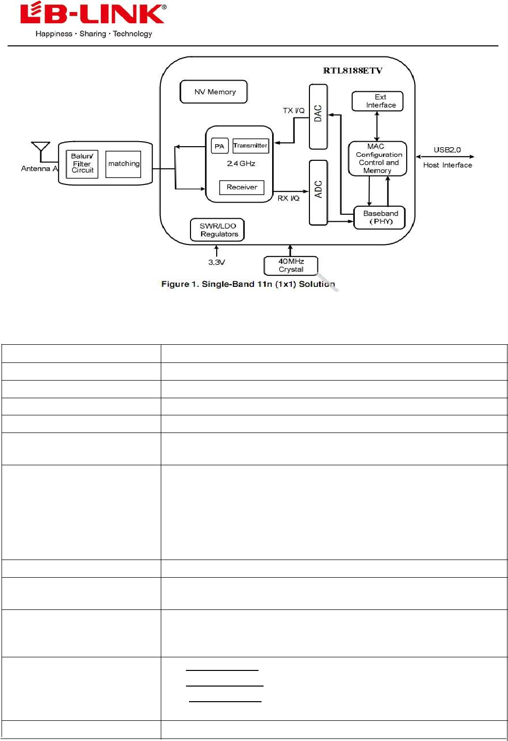
3.1 Function Block diagram.............................................................................................................................. 2
3.2 Electrical and Performance Specification................................................................................................... 3
3.3 DC Characteristic.........................................................................................................................................4
3.4 RF Characteristic......................................................................................................................................... 5
3.5 Product Photo............................................................................................................................................. 5
3.6 Mechanical Specification............................................................................................................................ 7
3.7 Product Pin Definition.................................................................................................................................7
4. Supported platform..........................................................................................................................................
....................................................................................................................................................................................................................................................................................
..........................................................................................................................................8
5. Peripheral Schematic Reference Design..........................................................................................................
....................................................................................................................................................................................................................
..........................................................................................................8
5.1 WiFi RF Circuit reference pictures.............................................................................................................. 9
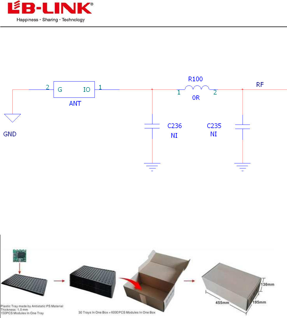
6. Package Information........................................................................................................................................
................................................................................................................................................................................................................................................................................
........................................................................................................................................9
7. Typical Solder Reflow Profile...........................................................................................................................
......................................................................................................................................................................................................................................................
...........................................................................................................................9

B-LINK ELECTRONIC CO., LTD in shenzhen
2
0. Revision History
Date Document
revision
Product
revision
Change Description
2014/06/18 1.0 V2.7 Update format ,change product size tolerance.
1. General Description
BL-8188EU1 product is designed base on Realtek RTL8188ETV chipset .It combines CMOS MAC,
Baseband PHY and RF in a single chip for IEEE 802.11a/b/g/n compatible. It supports IEEE802.11i
safety protocol, along with IEEE 802.11e standard service quality. It supports the new data
encryption on 64/128 bit WEP and safety mechanism on WPA-PSK/WPA2-PSK, WPA/WPA2. It can
implement the wireless network function on the laptop/desktop/MID and other wireless devices
easily . This module has implemented some efficient mechanisms in its software and hardware to
maximize the performance.
2. The range of applying
MID, networking camera, STB GPS, E-book, Hard disk player, Network Radios, PSP and other device
which need be supported by wireless networking.
3. Product Specification
3.1 Function Block diagram
B-LINK ELECTRONIC CO., LTD in shenzhen
3
3.2 Electrical and Performance Specification
Item Description
Product Name BL-R8188EU1
Major Chipset RTL8188ETV
Host Interface USB2.0
Standard IEEE 802.11b, IEEE 802.11g,IEEE 802.11n,
Frequency Range 2.4GHz~2.4835GHz
Modulation Type
802.11b: CCK, DQPSK, DBPSK
802.11g: 64-QAM,16-QAM, QPSK, BPSK
802.11n: 64-QAM,16-QAM, QPSK, BPSK
Working Mode Infrastructure, Ad-Hoc
Data Transfer Rate 1,2,5.5,6,11,12,18,22,24,30,36,48,54,60,90,120 and
maximum of 150Mbps
Spread Spectrum
IEEE 802.11b: DSSS (Direct Sequence Spread Spectrum)
IEEE 802.11g/n:OFDM (Orthogonal Frequency Division
Multiplexing)
Sensitivity @PER
1M: -90dBm@8%PER
6M: -88dBm@10%PER
11M:-86dBm@8%PER
54M:-73dBm@10%PER
Antenna Gain External 2dbi antenna,damping 50dbm in shielding box
B-LINK ELECTRONIC CO., LTD in shenzhen
4
RF Power >16dBm@11b, >14dBm@11g , >13dBm@11n,
Antenna type Connect to the external antenna through the half hole
The transmit distance Indoor 100M, Outdoor 300M, according the local environment
Dimension(L*W*H) 13.0 x 12.3 x 1.55mm (LxWxH) ;Tolerance: +-0.2mm
Power supply 3.3V +/-0.2V
Power Consumption standby mode 140mA@3.3V ,
TX mode 280mA@3.3V
Clock source 40MHz
Working Temperature 0ºC to +70ºC
Storage temperature -40°C ~ +85°C
3.3 DC Characteristic
Terms Contents
Specification : IEEE802.11b
Mode DSSS / CCK
Frequency 2412 – 2484MHz
Data rate 1, 2, 5.5, 11Mbps
DC Characteristics min Typ. max. unit
TX mode 300 310 320 mA
Rx mode 148 150 155 mA
Sleep mode 140 145 146 mA
Specification : IEEE802.11g
Mode OFDM
Frequency 2412 - 2484MHz
Data rate 6, 9, 12, 18, 24, 36, 48, 54Mbps
DC Characteristics min Typ. max. unit
TX mode 280 285 288 mA
Rx mode 140 145 150 mA
Sleep mode 143 145 146 mA
Specification : IEEE802.11n
Mode OFDM
Frequency 2412 - 2484MHz
Data rate 6.5, 13, 19.5, 26, 39, 52, 58.5, 65Mbps
DC Characteristics min Typ. max. unit
TX mode 280 286 230 mA
Rx mode 148 150 150 mA
Sleep mode 144 145 146 mA
B-LINK ELECTRONIC CO., LTD in shenzhen
5
3.4 RF Characteristic
Mode Rate(Mbps) Power(dBm) EVM(dB) Sensitivity(dBm)
CH1 CH7 CH13 CH1 CH7 CH13 CH1 CH7 CH13
11b
1 17.52 17.45 17.39 -28.36 -28.00 -27.95 -95 -95 -95
2 17.35 17.36 17.52 -24.38 -25.30 -25.20 -92 -92 -92
5.5 17.98 17.78 17.85 -24.21 -24.18 -24.01 -88 -88 -88
11 18.00 17.86 17.77 -23.51 -24.11 -24.30 -86 -86 -86
11g
6 15.20 15.31 15.42 -32.01 -31.52 -31.06 -90 -90 -90
9 15.10 15.11 15.42 -32.05 -31.75 -32.99 -88 -88 -88
12 14.86 14.98 14.79 -31.50 -31.78 -31.89 -86 -86 -86
18 14.58 14.68 14.96 -32.06 -31.45 -31.66 -85 -85 -85
24 14.94 14.86 14.88 -32.04 -31.90 -31.78 -83 -83 -83
36 14.69 14.86 14.60 -31.44 -31.70 -32.00 -80 -80 -80
48 14.90 14.800 14.77 -32.01 -32.01 -31.88 -75 -75 -75
54 14.88 14.90 15.00 -33.12 -32.72 -32.20 -73 -73 -73
11n
HT20
MCS0 15.11 15.21 15.42 -32.25 -31.75 -32.99 -90 -90 -90
MCS1 14.87 14.88 14.78 -31.52 -31.28 -31.29 -87 -87 -87
MCS2 14.68 14.78 14.66 -32.26 -31.45 -31.66 -85 -85 -85
MCS3 14.84 14.76 14.38 -32.24 -31.92 -31.28 -82 -82 -82
MCS4 15.12 15.21 15.44 -32.05 -31.25 -32.29 -79 -79 -79
MCS5 14.76 14.88 14.43 -31.50 -31.28 -31.29 -74 -74 -74
MCS6 14.68 14.78 14.34 -32.06 -31.42 -31.26 -71 -71 -71
MCS7 14.84 14.76 14.80 -32.04 -31.92 -31.28 -70 -70 -70
Mode Rate(Mbps) Power(dBm) EVM(dB) Sensitivity(dBm)
CH3 CH7 CH11 CH3 CH7 CH11 CH3 CH7 CH11
11n
HT40
MCS0 15.41 15.44 15.42 -32.45 -31.74 -32.94 -88 -88 -88
MCS1 14.47 14.48 14.70 -31.42 -31.58 -31.24 -84 -84 -84
MCS2 14.64 14.74 14.65 -31.27 -31.48 -31.06 -82 -82 -82
MCS3 14.54 14.56 14.58 -31.24 -31.32 -32.08 -78 -78 -78
MCS4 15.12 15.21 15.44 -32.05 -31.25 -32.29 -74 -74 -74
MCS5 14.77 14.89 14.44 -31.51 -31.29 -31.30 -71 -71 -71
MCS6 14.69 14.76 14.75 -32.17 -31.43 -31.27 -70 -70 -70
MCS7 14.74 14.70 14.82 -32.15 -31.93 -31.29 -68 -68 -68
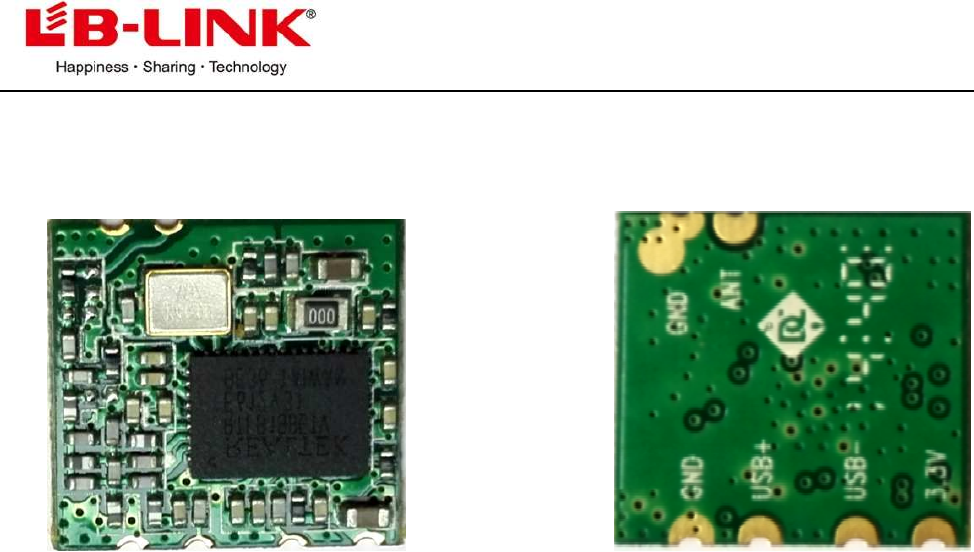
3.5 Product Photo
B-LINK ELECTRONIC CO., LTD in shenzhen
6
TOP Bottom
B-LINK ELECTRONIC CO., LTD in shenzhen
7
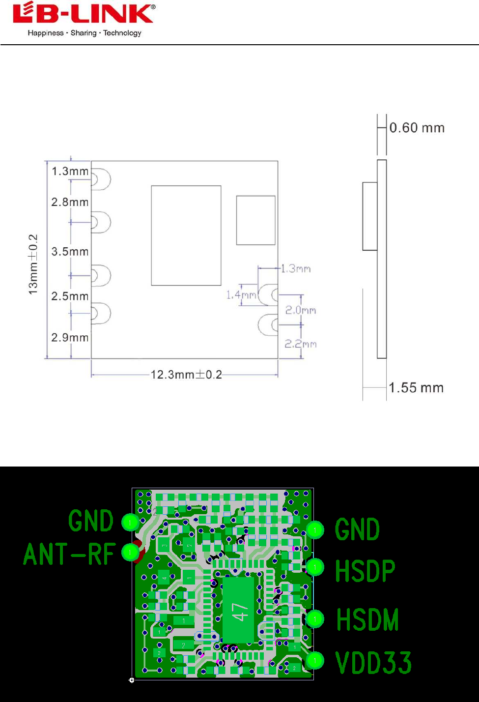
3.6 Mechanical Specification
Module dimension: Typical (L x W x H): 13mmx12.3mmx1.55mm Tolerance : +/-0.2mm
3.7 Product Pin Definition
B-LINK ELECTRONIC CO., LTD in shenzhen
8
4. Supported platform
Operating System CPU Framework Driver
WIN2000/XP/VISTA/WIN7 X86 Platform Enable
LINUX2.4/2.6 ARM, MIPSII Enable
WINCE5.0/6.0 ARM ,MIPSII Enable
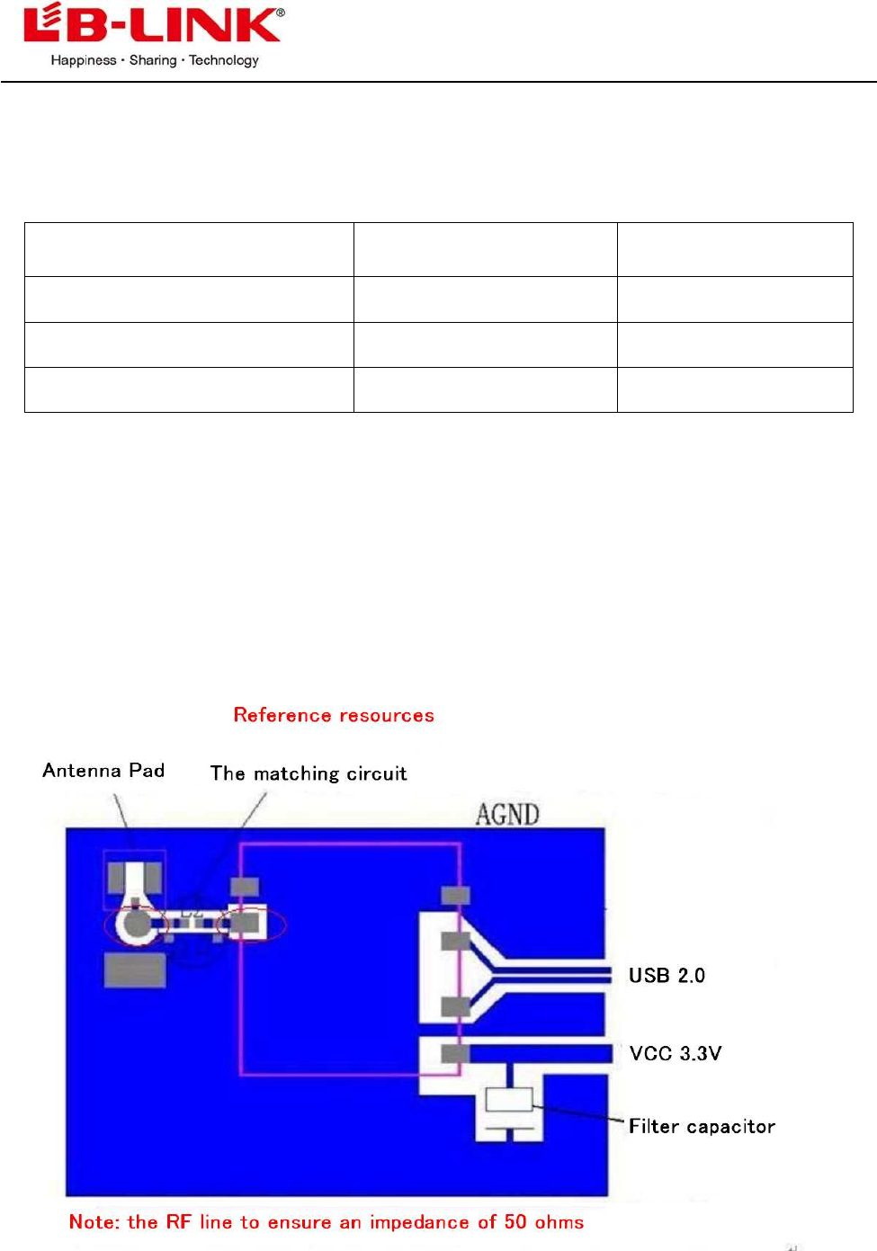
5. Peripheral Schematic Reference Design
(Layout suggestion)
B-LINK ELECTRONIC CO., LTD in shenzhen
9
5.1 WiFi RF Circuit reference pictures
6. Package Information
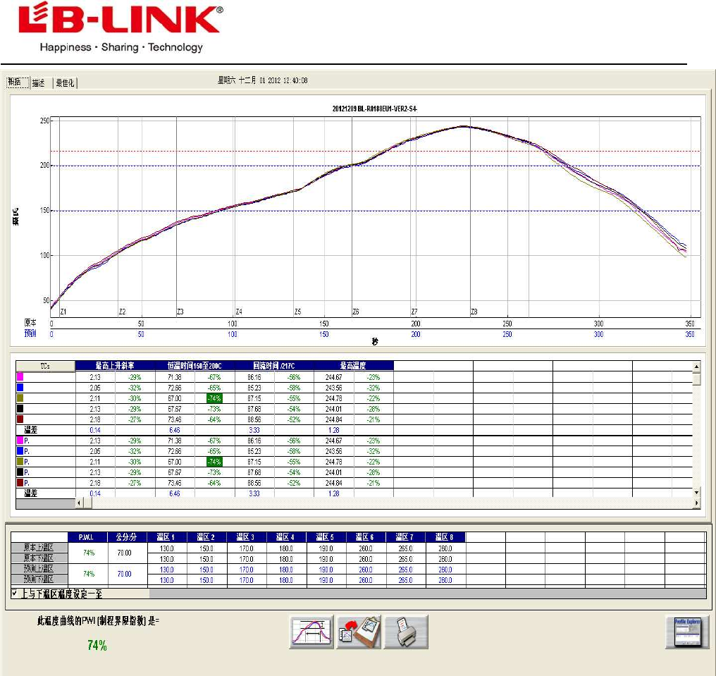
7. Typical Solder Reflow Profile
B-LINK ELECTRONIC CO., LTD in shenzhen
10
FCC Statement
This device complies with part 15 of the FCC Rules. Operation is subject to the following two conditions: (1) This
device may not cause harmful interference, and (2) this device must accept any interference received, including
interference that may cause undesired operation.
Any Changes or modifications not expressly approved by the party responsible for compliance could void the user's
authority to operate the equipment.
Note: This equipment has been tested and found to comply with the limits for a Class B digital device, pursuant to
part 15 of the FCC Rules. These limits are designed to provide reasonable protection against harmful interference
in a residential installation. This equipment generates uses and can radiate radio frequency energy and, if not
installed and used in accordance with the instructions, may cause harmful interference to radio communications.
However, there is no guarantee that interference will not occur in a particular installation. If this equipment does
cause harmful interference to radio or television reception, which can be determined by turning the equipment off
and on, the user is encouraged to try to correct the interference by one or more of the following measures:
-Reorient or relocate the receiving antenna.
-Increase the separation between the equipment and receiver.
-Connect the equipment into an outlet on a circuit different from that to which the receiver is connected.
-Consult the dealer or an experienced radio/TV technician for help.
The 150Mbps Wireless N SDIO
Module is designed to comply with the FCC statement. FCC ID is S8J-R8188EUG. The host system using 150
Mbps Wireless N SDIO Module, should have label indicated it contain modular’s
FCC ID:S8J-R8188EUG.
This radio module must not installed to colocate and operating simultaneously with other radios in host system
additional testing and equipment authorization
may be required to operating simultaneously with other radio.
RF warning for Mobile device:
This equipment complies with FCC radiation exposure limits set forth for an uncontrolled environment. This
equipment should be installed and operated with minimum distance 20cm between the radiator & your body.