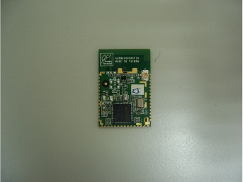
Billion Electric BIL-MD1000 ZigBee Module User Manual
Billion Electric Co., Ltd. ZigBee Module Users Manual
Users Manual

Billion ZigBee Module
User Manual
(MD1000)
DESCRIPTION
The MD1000 module is a ZigBee™ network solution that integrates a 2.4Ghz, IEEE
802.15.4-compliant transceiver with a 32 bit ARM® Cortex M3microprocessor. It contains
integrated Flash and RAM memory and peripherals of use to designers of ZigBee-based
applications.
The transceiver utilized an efficient architecture in which the integrated receiver channel
filtering allows for co-existence with other communication standards in the 2.4Ghz
spectrum such as Wi-Fi and Bluetooth. An optional high performance radio mode (boost
mode) is software selectable to boost dynamic range by a further 8dB. The highly
integrated antenna, power regulator, and Xtal keep the external component count low. The
internal PCB traced antenna and an external U.FL connector port is user selectable. This is
maximum the flexibility for the designer to minimize the cost or maximize the system
performance.
The EM357 has 192kB of embedded Flash memory and 12kB of integrated RAM for data
and program storage. The EM357 software stack employs an effective wear-leveling
algorithm in order to optimize the lifetime of the embedded Flash.
To support user-defined application, a number of peripherals such as GPIO, UART, SPI,
I2C, ADC, and general purpose timers are integrated. Also, an integrated voltage regulator,
power-on-reset circuitry, sleep timer, and low-power sleep modes are available. The deep
sleep mode draws less than 2uA, allowing products to achieve long battery life. The
equipped internal watch-dog timer allows the system to be reactivated once the system go
into a dead-lock state. This mechanism makes the system more reliable and available.
Target application for the MD1000 includes:
• Home automation and control
• Building automation and control
• Smart energy monitoring and control
• Tele-healthcare
• Asset tracking
The information of this document is subject to change without prior notice.
1

GENERAL FEATURES
Ember™ EM357 platform
192KB Flash memory, with option read protection
12KB SRAM
32-bit ARM® Cortex M3 microprocessor
24 general purpose I/O ports
DMA-SPI, I2C and UART interfaces
Integrated 12-bit resolution ADC
Designed for EmberZNet ZigBee Pro compliant networks
Miniature footprint: 2cm x 3cm
Integrated PCB trace antenna and U.FL external antenna connector
16 RF channels
Over indoor 30m and outdoor visual contact 100m of range
JTAG interface
AES 128-bit encryption
Low power consumption
Constant RF out power over 2.1~3.6 V voltage range
FCC and NCC certified
RoHS compliant
Product Specification
Chip Set Ember EM357 SoC
Operation Voltage 2.1~3.6V
Network Standard IEEE 802.15.4
Modulation DSSS PHY employing Offset-QPSK
Network Architectures Star or Mesh
Data Rate 250Kbps
Integrated Memory 192KB of Flash, 12KB of SRAM
Power Consumption TX: under 40mA, RX: under 40mA
Deep sleep: under 2uA
Watchdog Internal watchdog timer and power-on-reset circuitry
Encryption Integrated 128-bit AES encryption accelerator
Operating Frequency Band 2.405Ghz ~ 2.480Ghz (16 Channels with 5Mhz wide)
Antenna Type 1. Internal PCB Traced Planar Inverted-F Antenna
2. U.FL Connector for External Antenna
TX Output Power Max. +3dBm (+8dBm in Boost mode) , Min. -43dbm
2

RX Sensitivity Typical -100dBm(-101dBm in Boost mode) at 1% packet error rate
Operating Temperature (Ambient)
-40 °C ~ +85 °C
Humidity (Non-condensing) 0~95% RH
I/O PIN ASSIGNMENT
Pin # Name Direction
Description
1 GND Ground Ground
2 NC NC No connection
3 GND Ground Ground
4 GND Ground Ground
5 GND Ground Ground
6 NC NC No connection
7 VCC Power 3.3V power supply input (2.1V~3.6V)
8 VCC Power 3.3V power supply input (2.1V~3.6V)
9 nReset I Reset input (>26usec, active low)
10 PC5 I/O GPIO
11 PC6 I/O GPIO
12 PC7 O ZigBee status LED output (current: 4mA)
13 PA7 I/O GPIO
14 PB3 I UART CTS input
15 GND Ground Ground
16 GND Ground Ground
17 PB4 O UART RTS output
18 PA0 O SC2MOSI (OTA)
19 PA1 I SC2MISO (OTA)
20 PA2 O SC2SCLK (OTA)
21 PA3 O SC2nSSEL (OTA)
22 PA4 I/O GPIO
23 PA5 I/O GPIO
24 PA6 I/O GPIO
25 PB1 O UART TXD output
26 PB2 I UART RXD input
27 JTCK I JTAG JTCK
28 JTDO-PC2 O JTAG JTDO
29 JTDI-PC3 I JTAG JTDI
30 GND Ground Ground
31 GND Ground Ground
32 JTMS-PC4 I JTAG JTMS
33 PB0 I/O GPIO
34 PC1 I/O GPIO
35 JRST-PC0 I JTAG JRST
36 NC NC No connection
3

37 PB6 I ZigBee WPS input
38 VCC Power 3.3V power supply input
39 ANT_0 I Internal Antenna: ANT_0 = High, ANT_1 = Low input (default)
External Antenna: ANT_0 = Low, ANT_1 = High input
Pin # Name Direction Description
40 ANT_1 I Internal Antenna: ANT_0 = High, ANT_1 = Low input (default)
External Antenna: ANT_0 = Low, ANT_1 = High input
41 GND Ground Ground
42 GND Ground Ground
43 GND Ground Ground
44 NC NC No connection
45 GND Ground Ground
4

ELECTRICAL CHARACTERISTICS
Absolute Maximum Ratings
Parameter
Min.
Typ.
Max.
Unit
Power supply voltage -0.3 3.6 V
Voltage on any digital pin -0.3 VCC + 0.3
Max 3.6
V
Operation temperature range -40 85 °C
Storage temperature range -40 125 °C
Note: Exceeding the maximum ratings may cause permanent damage to the module or devices.
Operating Conditions
Paramete
r
Min.
Typ.
Max.
Unit
Power supply voltage 2.1 3.6 V
Input current for logic 0 -0.5 µA
Input current for logic 1 0.5 µA
Input voltage for logic 0 0 20% VCC
V
Input voltage for logic 1 80% VCC
VCC V
Output voltage for logic 0 0 18% VCC
V
Output voltage for logic 1 82% VCC
VCC
V
Input pull-up resistor value 24
29 34
KΩ
Input pull-down resistor value 24
29 34
KΩ
Output source current (standard current pad) 4
mA
Output sink current (standard current pad) 4
mA
Output source current
high current pad: PA6,PA7,PB6,PB7,PC0 8
mA
Output sink current
high current pad: PA6,PA7,PB6,PB7,PC0 8
mA
Ambient temperature range -40 25 +85 °C
5

DC Characteristics
Parameter
Min.
Typ.
Max.
Unit
Active Current (TX)
TX, Normal Mode, +3 dBm 31 mA
TX, Boost Mode, +8 dBm 39 mA
TX, Normal Mode, 0 dBm 28.5 mA
Active Current (RX)
RX, Normal Mode, +3 dBm 26 mA
RX, Boost Mode, +8 dBm 27 mA
summarizes the DC characteristics at 25°C and VDD of 3V of the EM35x Module.
RF Characteristics (@25°C, VCC=3.3V)
Parameter
Min.
Typ.
Max.
Unit
Frequency Range 2405 2480 MHz
Channel Spacing 5 MHz
RX Sensitivity (1% PER, 20-byte packet)
Normal Mode -100 -94 dBm
Boost Mode -101 -95 dBm
Adjacent Channel Rejection
High Side 35 dB
Low Side 35 dB
2nd High Side 43 dB
2nd Low Side 43 dB
All other channels 40 dB
TX Power (Maximum) dB
Boost Mode 8 dBm
Normal Mode 3 dBm
Error Vector Magnitude (Offset EVM) (per IEEE 802.15.4-2003)
5 15 %
6
7
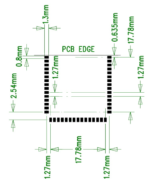
PCB COPPER PATTERN LAYOUT
8
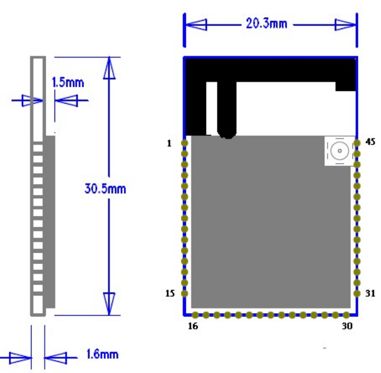
DIMENSIONS
9

Placement Guideline
It is recommended that MD1000 be placed on the corner of the main board and near
the edge as shown below.
10
Federal Communication Commission Interference Statement
This equipment has been tested and found to comply with the limits for a Class B digital device,
pursuant to Part 15 of the FCC Rules. These limits are designed to provide reasonable protection
against harmful interference in a residential installation. This equipment generates, uses, and can
radiate radio frequency energy and, if not installed and used in accordance with the instructions,
may cause harmful interference to radio communications. However, there is no guarantee that
interference will not occur in a particular installation. If this equipment does cause harmful
interference to radio or television reception, which can be determined by turning the equipment off
and on, the user is encouraged to try to correct the interference by one or more of the following
measures:
Reorient or relocate the receiving antenna.
Increase the separation between the equipment and receiver.
Connect the equipment into an outlet on a circuit different from that to which the receiver is
connected.
Consult the dealer or an experienced radio/TV technician for help.
FCC Caution:
This device complies with Part 15 of the FCC Rules. Operation is subject to the following two
conditions:
(1) This device may not cause harmful interference
(2) This device must accept any interference received, including interference that may cause
undesired operation.
Any changes or modifications not expressly approved by the party responsible for compliance could
void the user's authority to operate this equipment. . This device and its antenna(s) must not be co-
located or operating in conjunction with any other antenna or transmitter.
Co-location statement
This device and its antenna(s) must not be co-located or operating in conjunction with any other
antenna or transmitter.
FCC Radiation Exposure Statement
This equipment complies with FCC radiation exposure limits set forth for an uncontrolled
environment. This equipment should be installed and operated with minimum distance 20cm
between the radiator & your body.
11
This module is intended for OEM integrator. The OEM integrator is responsible for the compliance to
all the rules that apply to the product into which this certified RF module is integrated. Additional
testing and certification may be necessary when multiple modules are used.