Biostar M7Vig 400 Owners Manual VIG40414c
2014-07-31
: Biostar Biostar-M7Vig-400-Owners-Manual biostar-m7vig-400-owners-manual biostar pdf
Open the PDF directly: View PDF ![]() .
.
Page Count: 60

M
M
M7
7
7V
V
VI
I
IG
G
G
4
4
40
0
00
0
0
i
FCC Information and Copyright
This equipment has been tested and found to comply with the limits of a
Class B digital device, pursuant to Part 15 of the FCC Rules . T hese limits
are designed to provide reasonable protection against harmful
interference in a residential installation. This equipment generates, uses
and can radiate radio frequency energy and, if not installed and used in
accordance with the instructions, may cause harmful interference to radio
communications . There is no guarantee that interference will not occur in
a partic ular installation.
The vendor makes no representations or warranties with respect to the
contents here of and specially disclaims any implied warranties of
merchantability or fitness for any purpose. F urther the vendor reserves
the right to revise this publication and to make changes to the contents
here of without obligation to notify any party beforehand.
Duplication of this publication, in part or in whole, is not allowed without
firs t obtaining the vendor’s approval in writing.
The content of this user’s manual is subject to be changed without notice
and we will not be responsible for any mistakes found in this user’s
manual. All the brand and product names are trademarks of their
respective companies.

C
C
Co
o
on
n
nt
t
te
e
en
n
nt
t
ts
s
s
ii
LAYOUT OF M7VIG 400......................................................................... 1
COMPONENT INDEX............................................................................. 2
M7VIG 400 SYSTEM STRUCTURE...................................................... 3
ENGLISH................................................................................................... 4
M7VIG 400 Features...................................................................................4
Package contents.......................................................................................5
How to set up Jumper.................................................................................6
CPU Installation.........................................................................................6
DDR DIMM Modules: DDR1, DDR2................................................................7
Installing DDR Module................................................................................8
Jumpers, Headers, Connectors & Slots.........................................................8
FRANÇAIS .............................................................................................. 13
Caractéristiques de M7VIG 400..................................................................13
Contenu de l'Emballage............................................................................14
WARPSPEEDER™................................................................................. 15
Introduction.............................................................................................15
System Requirement................................................................................15
Installation..............................................................................................16
Usage.....................................................................................................17
TROUBLE SHOOTING......................................................................... 25
M
M
M7
7
7V
V
VI
I
IG
G
G
4
4
40
0
00
0
0
1
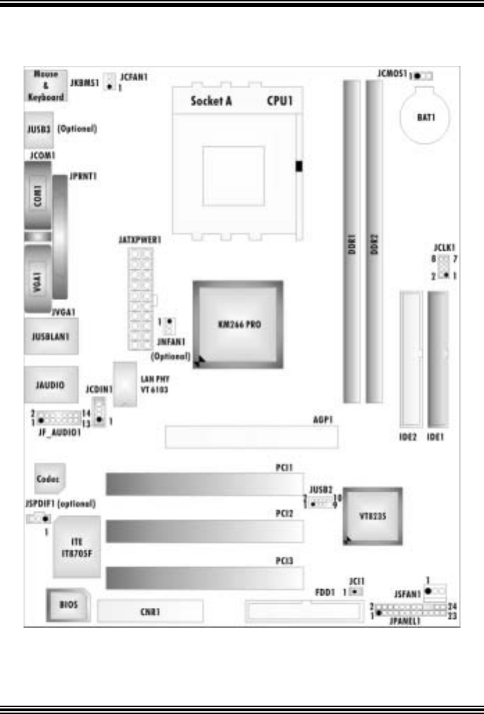
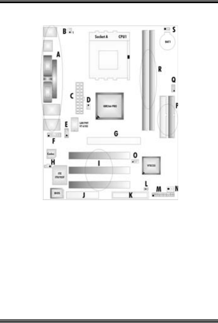
Layout of M7VIG 400
NOTE: ●represents the f irst pin.
M
M
M7
7
7V
V
VI
I
IG
G
G
4
4
40
0
00
0
0
2
Components Index
A. Back Panel Connectors K. Floppy Disk Connector (FDD1)
B. CPU Fan Connector (JCFAN1) L. Case Open Connector (JCI1)*
C. ATX Power Connector (JATXPW ER1) M. Front Panel Connector (JPANEL1)
D. North Bridge Fan Connector (JNFAN1)* N. System FAN Header (JSFAN1)
E. CD-ROM Audio-In Header (JCDIN1) O. Front USB Headers (JUSB2)
F. Front Audio Header (JF_AUDIO1) P. IDE Connectors (IDE1-2)
G. Accelerated Graphics Port Slot (AGP1) Q. Frequency Selection (JCLK1)
H. Digital Audio Connector (JSPDIF1)* R. DDR Modules (DDR1-2)
I. PCI BUS Slots (PCI 1-3) S. Clear CMOS Function (JCMOS1)
J. Communication Net work Riser Slot
(CNR1)* * stands for “optional”.
M
M
M7
7
7V
V
VI
I
IG
G
G
4
4
40
0
00
0
0
3
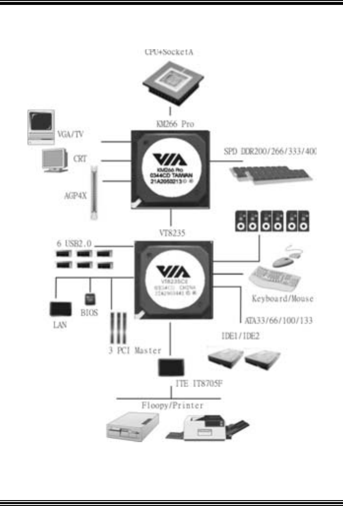
M7VIG 400 System Structure
M
M
M7
7
7V
V
VI
I
IG
G
G
4
4
40
0
00
0
0
4
English
M7VIG 400 Features
A. Har dware
CPU
Prov ides Soc k et A.
Supports single AMD® Athlon XP/ Duron Family processor.
Front Side Bus at 200/266/333 MHz.
Chipset
North Bridge: VIA KM266 Pro.
South Bridge: VIA VT8235.
Main Memory
Supports up to 2 DDR devices.
Supports SPD DDR 200/266/333/400 MHz (without ECC) DDR dev ices.
Maximum memory size is 2GB.
Super I/O
Chip: ITE8705F.
Prov ides the most commonly used legacy Super I/O functionality.
Env ironm ent C ont rol initiat iv es,
- H/W Monitor
- ITE's “Smart Guardian” function
Slots
Three 32-bit PCI bus master slots.
One CNR slot. (Optional)
One AGP 4X slot.
On Board IDE
Supports four IDE disk drives.
Supports PIO Mode 4, Master Mode and Ultra DMA 33/66/100/133 Bus Master
Mode.
LAN
PHY: VIA VT6103.
Supports 10 Mb/s and 100Mb/s auto-negotiation.
Half -Full duplex capability.
On Board AC’97 Sound Codec
Chip: CMI9761A.
Compliant with AC’97 specification.
Supports 6 channels.
Supports stereo microphone.
M
M
M7
7
7V
V
VI
I
IG
G
G
4
4
40
0
00
0
0
5
On Board Peripherals
a. Rear side
1 serial port.
1 VGA port.
1 parallel port. (SPP/EPP/ECP mode)
Audio ports in vertical position.
1 RJ-45 LAN jack.
PS/2 mouse and PS/2 keyboard.
4 USB2.0 ports.
b. Front Side
1 floppy port supports 2 FDDs with 360K, 720K, 1.2M, 1.44M and 2.88Mbytes.
2 USB2.0 ports.
1 front audio header.
1 S/PDIF Out header. (optional)
Dimensions
Micro ATX Form Factor: 19.4 cm X 24.4 cm (W X L)
B. BIOS & Software
BIOS
Award legal BIOS.
Supports APM1.2.
Supports ACPI.
Supports USB Function.
Software
Supports Warpspeeder™, 9th Touch™, FLASHER™
Off ers the highest performance for Windows 98 SE, Windows 2000, Windows Me,
Windows XP, UNIX Series etc.
Package contents
HDD Cable X 1
FDD Cable X 1
User’s Manual X 1
Fully Setup Driver CD X 1
StudioFun! Application CD X 1 (optional)
USB 2.0 Cable X 1 (optional)
S/PDIF Cable X 1 (optional)
Rear I/O Panel f or Micro ATX Case X 1 (optional)
M
M
M7
7
7V
V
VI
I
IG
G
G
4
4
40
0
00
0
0
6
How to set up Jumper
The illustration shows how to set up a jumper. When the Jumper cap is placed on pins, the
jumper is “close”. If no jumper cap is placed on the pins, the jumper is ”open”. The
illustration shows a 3-pin jumper whose pin 1 and 2 are “close” when jumper cap is placed
on these 2 pins.
Jumper open Jumper close Pin1-2 close
CPU Installation
Step1: Pull the lever sideway s away from the socket and then raise the lev er up to a
90-degree angle.
Step2: Look for the white dot/cut edge. The white dot/cut edge should point towards the
lev er piv ot. The CPU will f it only in the correct orientation.
Step3: Hold the CPU down f irmly, and then close the lever to complete the installation.
Step4: Put the CPU Fan on the CPU and buckle it. Connect the CPU fan power cable to
the JCFAN1. Then the installation is completed.
Ste p1 Step2 Step3 Step4

M
M
M7
7
7V
V
VI
I
IG
G
G
4
4
40
0
00
0
0
7
CPU Fan Header: JCFAN1
Pin Assignment
1 Ground
2 +12V
1
JCFAN1 3 FAN RPM rate Sense
System Fan Header: JSFAN1
Pin Assignment
1 Ground
2 +12V
1
JSFAN1 3 FAN RPM rate Sense
North Bridge Fan Header: JNFAN1 (optional)
Pin Assignment
1 Ground
2 +12V
1
JNFAN1 3 FAN RPM rate Sense
DDR DIMM Modules: DDR1, DDR2
DRAM Access Time: 2.5V Unbuffered/ SPD DDR 200 MHz (PC1600)/DDR 266
MHz (PC2100)/ DDR 333 MHz (PC2700)/DDR 400 MHz
(PC3200) Ty pe required.
DRAM Ty pe: 64MB/ 128MB/ 256MB/ 512MB/ 1GB DIMM Module (184 pin)
DIMM Socket
Location DDR Module Total Memor
y
Size (MB)
DDR 1 64MB/128MB/256MB/512MB/1GB
*1
DDR 2 64MB/128MB/256MB/512MB/1GB
*1
Max is
2GB
***Only for reference***
M
M
M7
7
7V
V
VI
I
IG
G
G
4
4
40
0
00
0
0
8
Installing DDR Module
1. Unlock a DIMM slot by pressing the retaining clips
outward. Align a DIMM to the slot in the way that
the notch of the DIMM matches the break of the
slot.
2. Insert the DIMM v ertically and firmly into the slot
until the retaining chip snap back in place and the
DIMM is properly seated.
Jumpers, Headers, Connectors & Slots
Floppy Disk Connector: FDD1
The motherboard provides a standard f loppy disk connector that supports 360K,
720K, 1.2M, 1.44M and 2.88M floppy disk types. This connector supports the
prov ided f loppy drive ribbon cables.
Hard Disk Connectors: IDE1/ IDE2
The motherboard has a 32-bit Enhanced PCI IDE Controller that provides PIO
Mode 0~5, Bus Master, and Ultra DMA 33/ 66/ 100/ 133 functionality. It has two
HDD connectors IDE1 (primary) and IDE2 (secondary).
The IDE connectors can connect a master and a slave driv e, so you can connect
up to f our hard disk driv es. The f irst hard drive should alway s be connected to
IDE1.
Peripheral Component Interconnect Slots: PCI 1-3
This motherboard is equipped with 3 standard PCI slots. PCI stands f or Peripheral
Component Interconnect, and it is a bus standard for expansion cards. This PCI
slot is designated as 32 bits.
Accelerated Graphics Port S lot: AGP1
Your monitor will attach directly to that v ideo card. This motherboard supports
video cards for PCI slots, but it is also equipped with an Accelerated Graphics Port
(AGP). An AGP card will take adv antage of AGP technology f or improved v ideo
efficiency and performance, especially with 3D graphics.
Communication Network Riser Slot: CNR1 (optional)
The CNR specification is an open Industry Standard Architecture, and it defines a
hardware scalable riser card interf ace, which supports modem only.
Case Open Connector: JCI1
Pin Assignment
1 Case Open Signal
1
JCI1 2 Ground
M
M
M7
7
7V
V
VI
I
IG
G
G
4
4
40
0
00
0
0
9
Front Panel Connector: JPANEL1
Power Connectors: JATXPWER1
PIN Assignment PIN Assignment
1 +3.3V 11 +3 . 3 V
2 +3.3V 12 -12V
3 Ground 13 Ground
4 +5V 14 PS_ON
5 Ground 15 Ground
6 +5V 16 Ground
7 Ground 17 Ground
8 PW_OK 18 -5V
9 Standby Voltage
+5V 19 +5V
JATXPWER1 10 +12V 20 +5V
SPK
PW R_ LED
HLED
SLP
RS T
224
IR
123
IRON/ OFF
(+ ) (- )
(+ ) (- )(+ )
Pin Assignment Function Pin Assignment Function
1 +5 V 2 Sleep Control
3 NA 4 Ground
Sleep
Button
5 NA 6 NA NA
7 Speaker
Speaker
Connector
8 Power LED (+)
9 HDD LED (+) 10 Power LED (+)
11 HDD LED (-)
Hard Drive
LED 12 Power LED (-)
POWER
LED
13 Ground 14 Power Button
15 Reset Control
Reset
Button 16 Ground
Power-on
Button
17 NA 18 KEY
19 NA 20 KEY
21 +5 V 22 Ground
23 IRTX
IrDA
Connector
24 IRRX
IrDA
Connector
JPAN EL 1
M
M
M7
7
7V
V
VI
I
IG
G
G
4
4
40
0
00
0
0
10
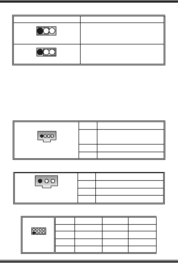
Clear CMOS Jumper: JCMOS1
JCMOS1 Assignment
1
Pin 1-2 Close
Normal Operation (default)
1
Pin 2-3 Close
Clear CMOS Data
※ Clear CMOS Procedures:
1. Remov e AC power line.
2. Set the jumper to “Pin 2-3 Close”.
3. Wait for fiv e seconds.
4. Set the jumper to “Pin 1-2 Close”.
5. Power on the AC.
6. Reset y our desired password or clear the CMOS data.
CD-ROM Audio-In Header: JCDIN1
Pin Assignment
1 Left Channel Input
2 Ground
3 Ground
1 4
JCDIN1
4 Right Channel Input
Digital Audio Connector: JSPDIF1 (optional)
Pin Assignment
1 +5V
2 SPDIF_OUT
13
JSPDIF1 3 Ground
Frequency Selection: JCLK1
Pin 100 MHz 133 MHz 166 MHz
1-2 Close Open Open
3-4 Close Close Open
5-6 Open Open Open
1
27
8
7-8 Open Open Open
M
M
M7
7
7V
V
VI
I
IG
G
G
4
4
40
0
00
0
0
11
Front Panel Audio Header: JF_AUDIO1
1
213
14
JF_AUDIO1
Pin Assignment Pin Assignment
1 Mic In/ Center 2 Ground
3 Mic Power/ Bass 4 Audio Power
5 Right Line Out/ Speaker Out
Right 6 Right Line Out/ Speaker Out Righ
t
7 Reserv ed 8 Key
9 Left Line Out/ Speaker Out
Left 10 Left Line Out/ Speaker Out Left
11 Right Line In/ Rear Speaker
Right 12 Right Line In/ Rear Speaker Right
13 Left Line In/ Rear Speaker Left 14 Left Line In/ Rear Speaker Left
Front USB Header: JUSB2
Pin Assignment Pin Assignment
1 +5V(f used) 2 +5V(fused)
3 USB- 4 USB-
5 USB+ 6 USB+
7 Ground 8 Ground
2
1
10
9
JUSB1/ JUSB2
9 KEY 10 NA
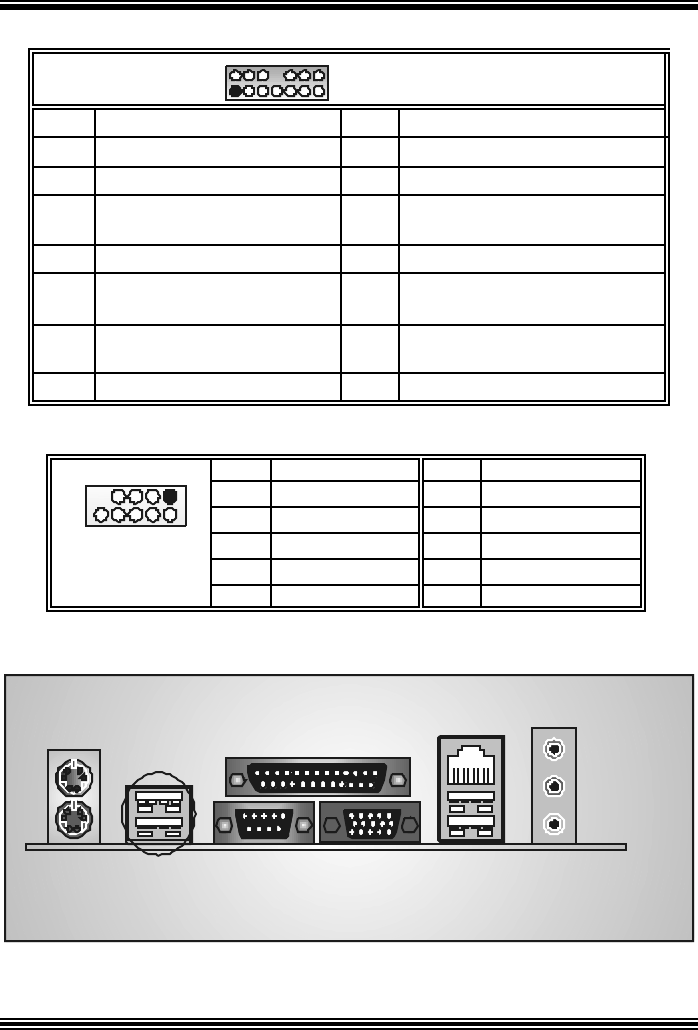
Back Panel Connectors
PS/2
Keyboard
PS/2
Mouse
COM1
Parallel Port
JP RNT1
JCOM1
JKB MS1
USB
JUSB3 JVGA1
VGA1 USB
JUSBLAN1
Speaker Out
Line In
Mic In
JAUDIO
LAN
(optional)
M
M
M7
7
7V
V
VI
I
IG
G
G
4
4
40
0
00
0
0
12
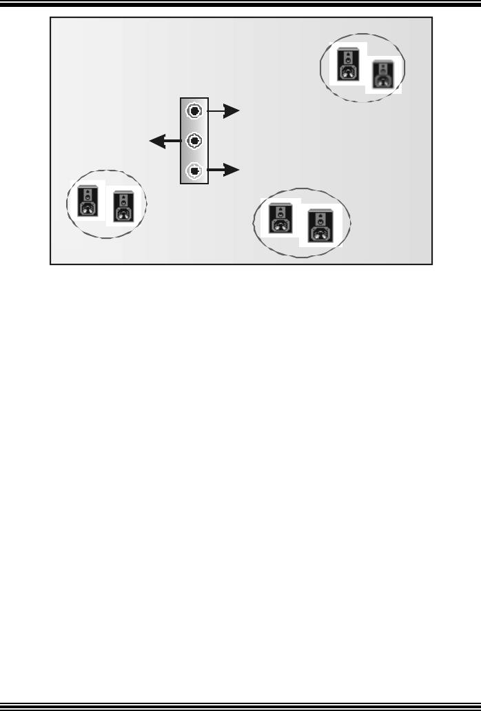
6 Channel Speakers
Speaker O ut/
Front Speaker
(Right & Left)
Line In/
Rear Speaker (Left & Right)
Mic In/ Center & Bass

M
M
M7
7
7V
V
VI
I
IG
G
G
4
4
40
0
00
0
0
13
Français
Caractéristiques de M7VIG 400
A. Ma tér ie l
Processeur
A v ec s o ck et A .
Prise en charge du processeur AMD® Athlon XP/Duron Family.
Bus f rontal à 200/266/333 MHz.
Jeu de puces
North Bridge : VIA KM266 Pro.
South Bridge : VIA VT8235.
Mémoire principale
Prise en charge de deux périphériques 2 DDR.
Prise en charge des périphériques SPD DDR 200/266/333/400 MHz (sans ECC).
Taille maximale de la mémoire :2Go.
Super E/S
Puce : ITE8705F.
Interf ace de Comptage de Broche Faible.
Offre la f onctionnalité Super E/S héritée la plus couramment utilisée.
Initiatives de Controle d’Env ironnement.
- Moniteur H/W
- Fonction “Smart Guardian” de ITE
Fentes
3 fentes Bus Master PCI à 32 bits.
Une f ente AGP 4X.
Une f ente CNR. (optionnel)
IDE intégré
Prise en charge de quatre lecteurs de disque IDE.
Prise en charge de PIO Mode 4 et Ultra DMA 33/66/100/133 Bus Master Mode.
LAN
PHY : VIA VT6103
Double Vitesse: 10/100Mbps.
Full/Half Duplex.
Négociation automatique : 10/100 Mbps, Full/Half Duplex.
M
M
M7
7
7V
V
VI
I
IG
G
G
4
4
40
0
00
0
0
14
AC’97 Sound Codec intégré
Puce: CMI 9761A
Conf orme aux spécif ications AC’97.
I nt erf ac e AC ’97 2. 3.
Prise en charge de 6 canaux.
Prise en charge de la microphone stereo.
Périphériques intégrés
a. Côté arrière
1 port série.
1 port VGA.
1 port parallèle (mode SPP/EPP/ECP)
1 port audio en position v erticale.
1 RJ-45 LAN Jack.
Souris PS/2 et clavier PS/2.
4 ports USB2.0.
b. Côté frontal
1 port disquette prenant en charge 2 FDD avec 360K, 720K, 1.2M, 1.44M et
2,88Mo.
2 ports USB2.0, 1 Embase Audio, 1 Embase de Sortie S/PDIF (optionnel).
Dimensions
Facteur de forme ATX : 19.4 cm x 24.4 cm. (Larg x L)
B. BIOS et logiciel
BIOS
Award legal Bios.
APM1.2.
ACPI.
Fonction USB.
Logiciel
Prise en charge de WarpspeederTM
, 9t h Touc hTM
, FLASHER™.
Offrant la meilleure performance pour Windows 98 SE, Windows 2000, Windows Me,
Windows XP, UNI X series etc .
Contenu de l'Emballage
Câble de Disque Dur X1
Câble de Lecteur de Disquette X1
Manuel d’utilisation X1
CD de Sollicitation StudioFun! X 1 (Optionnel)
Câble USB 2.0 X1 (Optionnel)
Panneau d’E/S Arrière pour Boîtier Flex X 1 (Optionnel)
CD de Pilote Complet X 1
Câble S/PDIF X 1 (optionnel)

M
M
M7
7
7V
V
VI
I
IG
G
G
4
4
40
0
00
0
0
15
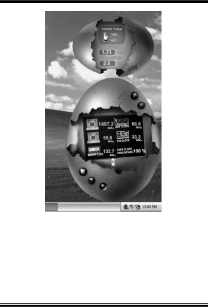
WarpSpeeder™
Introduction
[ WarpSpeeder™ ], a new powerf ul control utility, f eatures three user-friendly functions
including Ov erclock Manager, Ov ervoltage Manager, and Hardware Monitor.
With the Ov erclock Manager, users can easily adjust the frequency they prefer or they can
get the best CPU perf ormance with just one click. The Ov ervoltage Manager, on the other
hand, helps to power up CPU core v oltage and Memory voltage. The cool Hardware
Monitor smartly indicates the temperatures, voltage and CPU fan speed as well as the
chipset information. Also, in the About panel, you can get detail descriptions about BIOS
model and chipsets. In addition, the frequency status of CPU, memory, AGP and PCI
along with the CPU speed are synchronically shown on our main panel.
Moreov er, to protect users' computer systems if the setting is not appropriate when testing
and results in system f ail or hang, [ WarpSpeeder™ ] technology assures the system
stability by automatically rebooting the computer and then restart to a speed that is either
the original system speed or a suitable one.
System Requirement
OS Support: Windows 98 SE, Windows Me, Windows 2000, Windows XP
DirectX: DirectX 8.1 or above. (The Windows XP operating system includes DirectX 8.1. If
y ou use Windows XP, y ou do not need to install DirectX 8.1.)
M
M
M7
7
7V
V
VI
I
IG
G
G
4
4
40
0
00
0
0
16
Installation
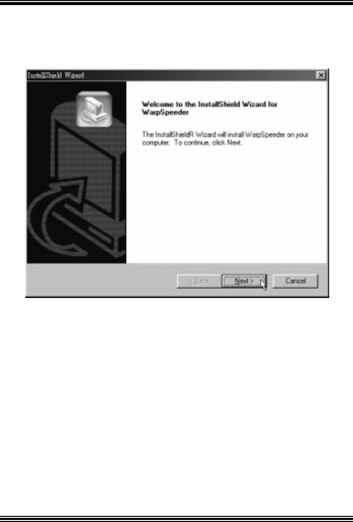
1. Execute the setup execution f ile, and then the following dialog will pop up.
Please click “Next” button and f ollow the default procedure to install.
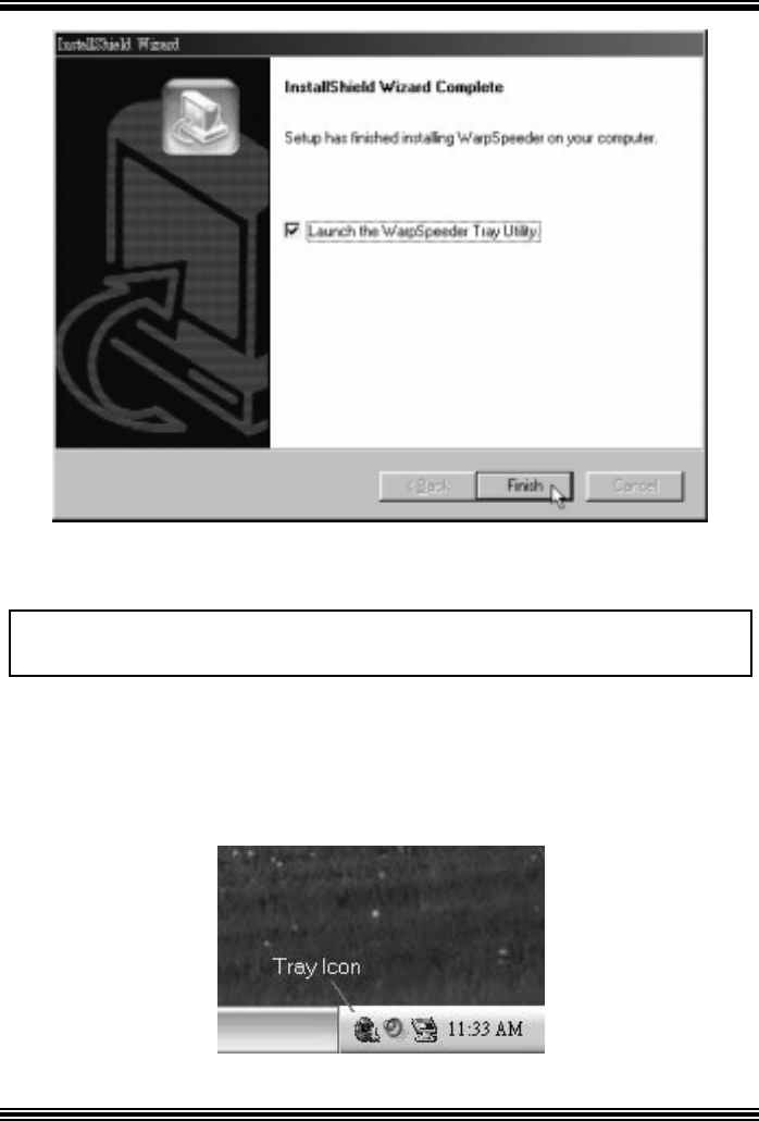
2. When y ou see the f ollowing dialog in setup procedure, it means setup is
completed. If the “Launch the WarpSpeeder Tray Utility ” checkbox is checked,
the Tray Icon utility and [WarpSpeeder™] utility will be automatically and
immediately launched after y ou click “Finish” button.
M
M
M7
7
7V
V
VI
I
IG
G
G
4
4
40
0
00
0
0
17
Usage
The following figures are just only for reference, the screen printed in this user manual will
change according to your motherboard on hand.
[WarpSpeeder™] includes 1 tray icon and 5 panels:
1. Tray Icon:
Whenev er the Tray Icon utility is launched, it will display a little tray icon on the right side of
Windows Taskbar.
M
M
M7
7
7V
V
VI
I
IG
G
G
4
4
40
0
00
0
0
18
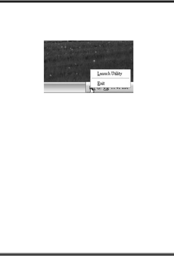
This utility is responsible f or conveniently invoking [WarpSpeeder™] Utility. You can use
the mouse by clicking the left button in order to inv oke [WarpSpeeder™] directly from the
little tray icon or you can right-click the little tray icon to pop up a popup menu as following
f igure. The “Launch Utility” item in the popup menu has the same function as mouse
left-click on tray icon and “Exit” item will close Tray Icon utility if selected.
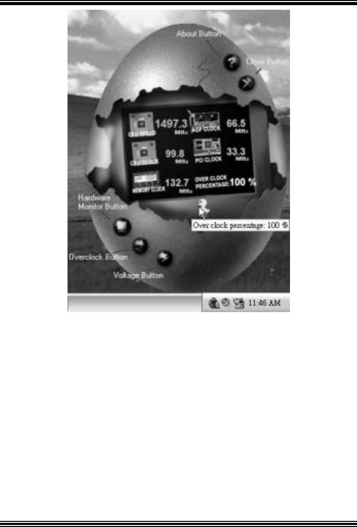
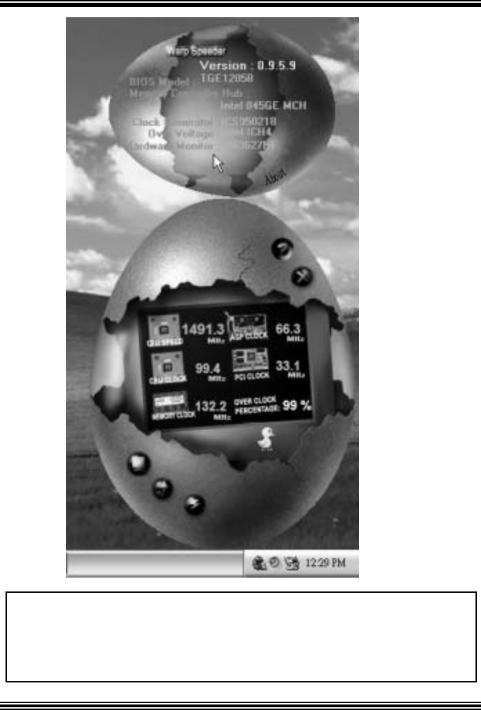
2. Main Panel
If you click the tray icon, [ WarpSpeeder™ ] utility will be inv oked. Please ref er
do the following f igure; the utility’s f irst window y ou will see is Main Panel.
Main Panel contains features as follows:
a. D is play t he C PU Speed, C PU ex t ernal cloc k, Mem ory cloc k, AGP c loc k, and PC I
clock inf ormation.
b. Contains About, Voltage, Overclock, and Hardware Monitor Buttons f or invoking
respective panels.
c. With a user-friendly Status Animation, it can represent 3 ov erclock percentage
stages:
Man walking => ov erclock percentage from 100% ~ 110 %
Panther running => overclock percentage from 110% ~ 120%
Car racing => ov erclock percentage f rom 120% ~ above
M
M
M7
7
7V
V
VI
I
IG
G
G
4
4
40
0
00
0
0
19
3. Voltage Panel
Click the Voltage button in Main Panel, the button will be highlighted and the Voltage
Panel will slide out to up as the f ollowing figure.
In this panel, you can decide to increase CPU core voltage and Memory voltage or not.
The def ault setting is “No”. If y ou want to get the best performance of ov erclocking, we
rec om m end y ou clic k t he option “Y es ”.
M
M
M7
7
7V
V
VI
I
IG
G
G
4
4
40
0
00
0
0
20
4. Overclock Panel
Click the Ov erclock button in Main Panel, the button will be highlighted and the Overclock
Panel will slide out to left as the f ollowing figure.
M
M
M7
7
7V
V
VI
I
IG
G
G
4
4
40
0
00
0
0
21
Overclock Panel contains the these features:
a. “–3MHz button”, “-1MHz button”, “+1MHz button”, and “+3MHz button”: provide user
the ability to do real-time overclock adjustment.
Warning: Manually overclock is potentially dangerous, especially when the
overclocking percentage is over 110 %. We strongly recommend you verify
every speed you overclock by click the Verify button. Or, you can just click
Auto overclock button and let [ WarpSpeeder™ ] automatically gets the best
result for you.
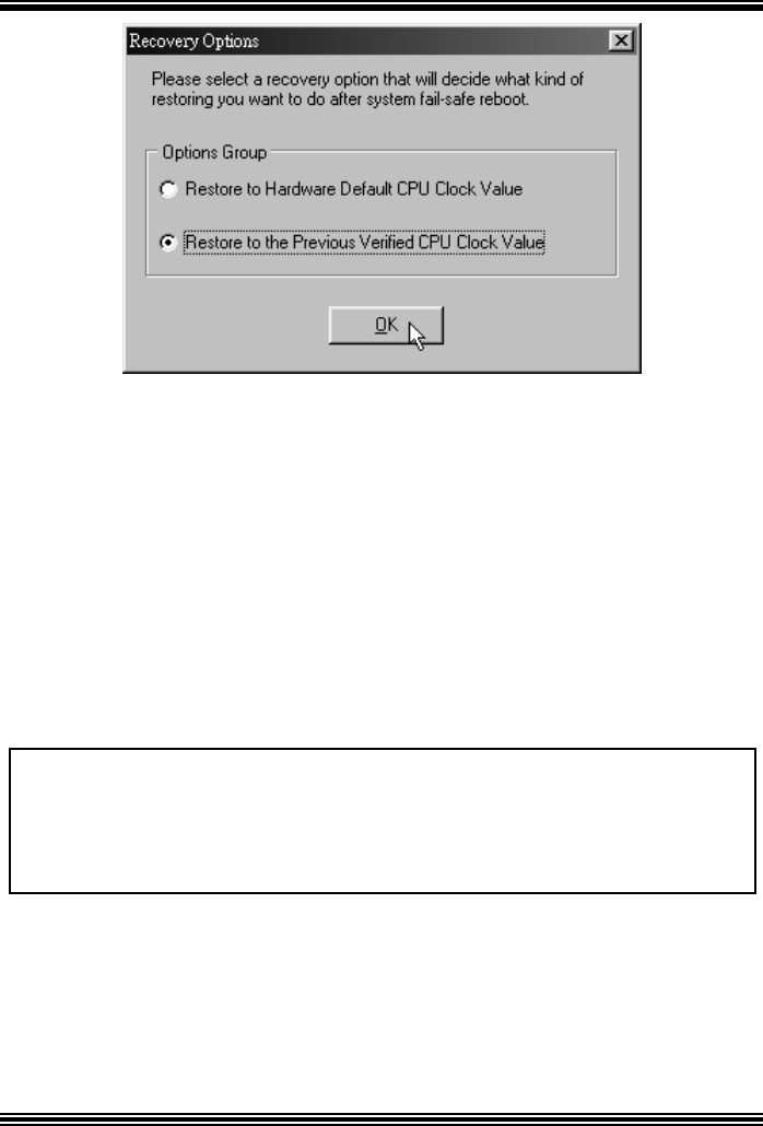
b. “Recovery Dialog button”: Pop up the following dialog. Let user select a restoring
way if system need to do a f ail-safe reboot.
M
M
M7
7
7V
V
VI
I
IG
G
G
4
4
40
0
00
0
0
22
d. “Auto-ov erclock button”: User can click this button and [ WarpSpeeder™ ] will set
the best and stable performance and frequency automatically. [ WarpSpeeder™ ]
utility will execute a series of testing until system f ail. Then system will do f ail-saf e
reboot by using Watchdog f unction. After reboot, the [ WarpSpeeder™ ] utility will
restore to the hardware default setting or load the verif ied best and stable
frequency according to the Recovery Dialog’s setting.
e. “Verify button”: User can click this button and [ WarpSpeeder™ ] will proceed a
testing f or current frequency. If the testing is ok, then the current f requency will be
saved into system registry. If the testing fail, system will do a fail-safe rebooting.
After reboot, the [ WarpSpeeder™ ] utility will restore to the hardware default
setting or load the verif ied best and stable frequency according to the Recovery
Dialog’s setting.
Note: Because the testing programs, invoked in Auto-overclock and Verify,
include DirectDraw , Direct3D and DirectShow tests, the DirectX 8.1 or newer
runtime library is required. And please make sure your display card’s color
depth is High color (16 bit) or True color( 24/32 bit ) that is required for
Direct3D rendering.
M
M
M7
7
7V
V
VI
I
IG
G
G
4
4
40
0
00
0
0
23
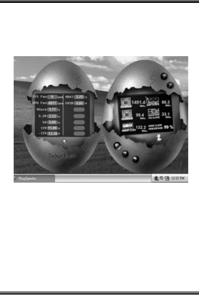
5. Hardware Monitor Panel
Click the Hardware Monitor button in Main Panel, the button will be highlighted and the
Hardware Monitor panel will slide out to left as the f ollowing figure.
In this panel, y ou can get the real-time status inf ormation of y our system. The information
will be ref reshed ev ery 1 second.
6. About Panel
Click the About button in Main Panel, the button will be highlighted and the About Panel
will slide out to up as the following f igure.
In this panel, you can get model name and detail inf ormation in hints of all the chipset that
are related to overclocking. You can also get the mainboard’s BIOS model and the
Version number of [ WarpSpeeder™ ] utility.
M
M
M7
7
7V
V
VI
I
IG
G
G
4
4
40
0
00
0
0
24
Note: Because the overclock, overvoltage, and hardware monitor features
are controlled by several separate chipset, [ WarpSpeeder™ ] divide these
features to separate panels. If one chipset is not on board, the correlative
button in Main panel will be disabled, but will not interfere other panels’
functions. This property can make [ WarpSpeeder™ ] utility more robust.
M
M
M7
7
7V
V
VI
I
IG
G
G
4
4
40
0
00
0
0
25
Trouble Shooting
PROBABLE SOLUTION
No power to the system at all Power light don’t
illuminate, fan inside power supply does not turn
on. Indicator light on keyboard does not turn on
* Make sure power cable is securely plugged in
* Rep l ac e c a bl e
* Contact techni c al s upp ort
PROBABLE SOLUTION
System ino
p
erative. Ke
y
board li
g
hts are on,
power indicator lights are lit, hard drive is
s p i n ni ng .
* Usin
g
even
p
ressure on both ends of th
e
DI M M,
p
ress down firml
y
until the modul
e
snaps into place.
PROBABLE SOLUTION
System does not boot from hard disk drive, can
be booted from CD-ROM drive. * Check cable runnin
g
from disk to disk controlle
r
board. Make sure both ends are securel
y
p
lu
gg
ed in; check the drive t
yp
e in th
e
standard CMOS setup.
* Backin
g
u
p
the hard drive is extremel
y
important. All hard disks are ca
p
able o
breaking down at any time.
PROBABLE SOLUTION
System only boots from CD-ROM. Hard disk can
be read and applications can be used but
booting from hard disk is impossible.
* Back u
p
data and a
pp
lications files. Reforma
the hard drive. Re-install a
pp
lications and dat
a
using backup disks.
PROBABLE SOLUTION
Screen message says “Invalid Configuration” or
“CMOS Failure.” * Review s
y
stem’ s e
q
ui
p
ment . Make sure
correct information is in setup.
PROBABLE SOLUTION
Cannot boot system after installin
g
second hard
drive. * Set master/slave jumpers correctly.
* Run SETUP
p
ro
g
ram and select correct driv
e
t
yp
es. Call drive manufacturers fo
r
compatibility with other drives.

M
M
M7
7
7V
V
VI
I
IG
G
G
4
4
40
0
00
0
0
26
4/14/2004

M7VIG 400 BIOS Setup
i
BIOS Setup........................................................................................1
1 Main Menu..................................................................................................... 3
2 Standard CMOS Features .............................................................................. 6
3 Advanced BIOS Features............................................................................... 9
4 Advanced Chipset Features.......................................................................... 12
5 Integrated Peripherals ..................................................................................16
6 Power Management Setup ........................................................................... 21
7 PnP/PCI Configurations ...............................................................................26
8 PC Health Status .......................................................................................... 29
9 Frequency/ Voltage Control......................................................................... 31

M7VIG 400 BIOS Setup
1
BIOS Setup
Introduction
T his manual discussed Award™ Setup program built into the ROM BIOS. T he Setup
program allows users to modify the basic system configuration. This special information is
then stored in battery-backed RAM so that it retains the Setup information when the power
is turned off.
T he Award BIOS™ installed in your computer system’s ROM (Read Only Memory) is a
custom version of an industry standard BIOS. This means that it supports AMD processor
input/output system. The BIOS provides critical low-level support for standard devices
such as disk drives and serial and parallel ports.
Adding important has customized the Award BIOS™, but nonstandard, features such as
virus and password protection as well as special support for detailed fine-tuning of the
chipset controlling the entire system.
The rest of this manual is intended to guide you through the process of configuring your
system using Setup.
Plug and Play Support
These AWARD BIOS supports the Plug and Play Version 1.0A specification. ESCD
(Extended System Configuration Data) write is supported.
EPA Green PC Support
This AWARD BIOS supports Version 1.03 of the EPA Green PC specification.
APM Support
These AWARD BIOS supports Version 1.1&1.2 of the Advanced Power Management
(APM) specification. Power management features are implemented via the System
Management Interrupt (SMI). Sleep and Suspend power management modes are supported.
Power to the hard disk drives and video monitors can be managed by this AWARD BIOS.
ACPI Support
Award ACPI BIOS support Version 1.0 of Advanced Configuration and Power interface
specification (ACPI). It provides ASL code for power management and device
configuration capabilities as defined in the ACPI specification, developed by Microsoft,
Intel and Toshiba.

M7VIG 400 BIOS Setup
2
PCI Bus Suppo rt
This AWARD BIOS also supports Version 2.1 of the Intel PCI (Peripheral Component
Interconnect) local bus specification.
DRAM Support
DDR SDRAM (Double Data Rate Synchronous DRAM) are supported.
Suppo rte d CP Us
T h is AW ARD BIO S s u pp o rt s the AM D C P U.
Us ing Setup
In general, you use the arrow keys to highlight items, press <Enter> to select, use the
<PgUp> and <PgDn> keys to change entries, press <F1> for help and press <Esc> to quit.
The following table provides more detail about how to navigate in the Setup program by
using the keyboard.
Keystroke Function
Up arrow Move to p revious item
Down a rrow Move to next item
Left arrow Move to the item o n the left (menu bar)
Right arrow Move to the item on the right (menu bar)
Move Enter Move to the item you desired
PgUp key Increase the numeric value or make changes
PgDn key Decrease the numeric value or make changes
+ Key Increase the numeric value or make changes
- Key Decrease the numeric value or make changes
Esc key Main Menu – Quit and not save changes into CMOS
Status Page Setup Menu and Option Page Setup Menu – Exit
Current page and return to Main Menu
F1 key Genera l help o n Setup navigation keys
F5 key Load previous values from CMOS
F7 key Load the optimized defaults
F10 key Save all the CMOS changes and exit
M7VIG 400 BIOS Setup
3
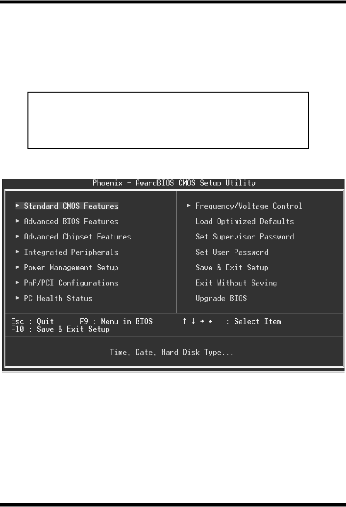
1 Main Menu
Once you enter Award BIOS™ CMOS Setup Utility, the Main Menu will appear on the
screen. The Main Menu allows you to select from several setup functions. Use the arrow
keys to select among the items and press <Enter> to accept and enter the sub-menu.
Figure 1. Main Menu
Standard CMOS Features
This submenu contains industry standard configurable options.
Advance d BIOS Features
This submenu allows you to configure enhanced features of the BIOS.
Advanced Chipset Features
This submenu allows you to configure special chipset features.
!! WARNING !!
The information about BIOS defaults on manual (Figu re
1,2,3,4,5,6,7,8,9) is just for reference, please refer to the BIOS
installed on board, for update information.
M7VIG 400 BIOS Setup
4
Integrated Peripherals
This submenu allows you to configure certain IDE hard drive options and Programmed
Input/ Output features.
Power Management Setup
This submenu allows you to configure the power management features.
PnP/PCI Configurations
This submenu allows you to configure certain “Plug and Play” and PCI options.
PC Health Status
This submenu allows you to monitor the hardware of your system.
Frequency/ Voltage Control
This submenu allows you to change CPU Vcore Voltage and CPU/PCI clock. (However,
this function is strongly recommended not to use. Not properly change the voltage
and clock may cause the CPU or M/B damage!)
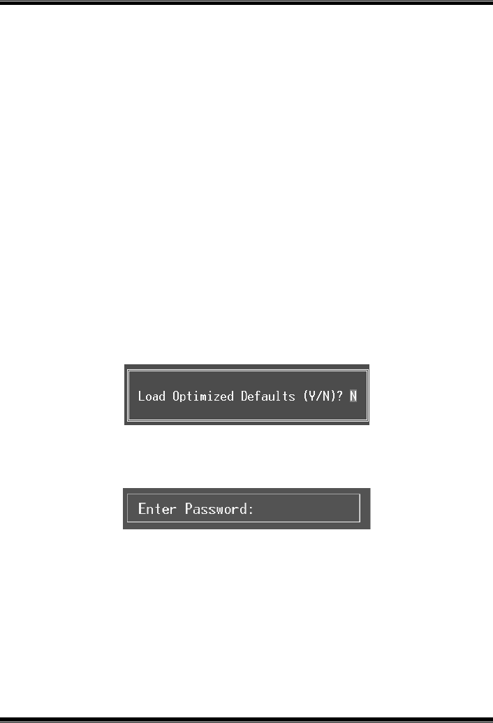
Load Opti mi ze d Defa ul ts
This selection allows you to reload the BIOS when the system is having problems
particularly with the boot sequence. These configurations are factory settings optimized
for this system. A confirmation message will be displayed before defaults are set.
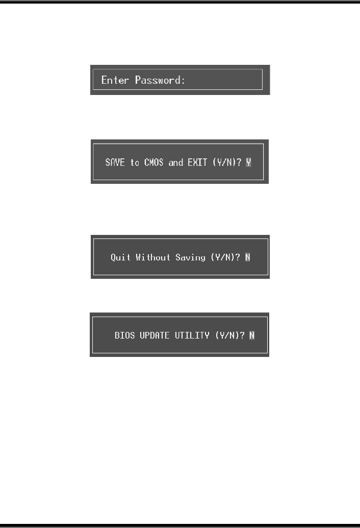
Set Supervisor Password
Setting the supervisor password will prohibit everyone except the supervisor from making
changes using the CMOS Setup Utility. You will be prompted with to enter a password.
M7VIG 400 BIOS Setup
5
Set User Password
If the Supervisor P assword is not set, then the User P assword will function in the same way
as the Supervisor Password. If the Supervisor P assword is set and the User P assword is
set, the “User” will only be able to view configurations but will not be able to change them.
Save & Exit Setup
Save all configuration changes to CMOS(memory) and exit setup. Confirmation message
will be displayed before proceeding.
Exit Without Saving
Abandon all changes made during the current session and exit setup. confirmation
message will be displayed before proceeding.
Upgrade BIOS
This submenu allows you to upgrade bios.
M7VIG 400 BIOS Setup
6
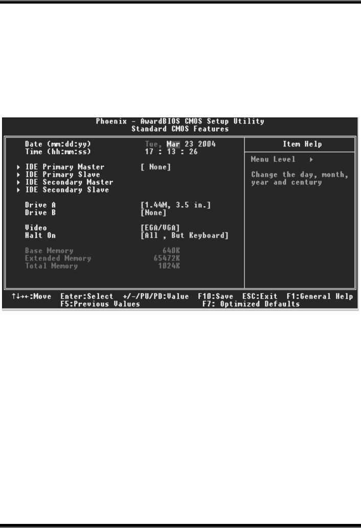
2 Standard CMOS Features
The items in Standard CMOS Setup Menu are divided into 10 categories. Each category
includes no, one or more than one setup items. Use the arrow keys to highlight the item and
then use the<PgUp> or <PgDn> keys to select the value you want in each item.
Figure 2. Standard CMOS Setup

M7VIG 400 BIOS Setup
7
Main Menu Selections
This table shows the selections that you can make on the Main Menu.
Item Options Description
Date mm : dd : yy Set the system date. Note
that the ‘Day’ automatically
changes when you set the
date.
Time hh : mm : ss Set the system internal
clock.
IDE Primary Master Options are in its sub
menu.
Press <Enter> to enter the
sub menu of detailed
options
IDE Primary Slave Options are in its sub
menu.
Press <Enter> to enter the
sub menu of detailed
options.
IDE Secondary Master Options are in its sub
menu.
Press <Enter> to enter the
sub menu of detailed
options.
IDE Secondary Slave Options are in its sub
menu.
Press <Enter> to enter the
sub menu of detailed
options.
Drive A
Drive B
360K, 5.25 in
1.2M, 5.25 in
720K, 3.5 in
1.44M, 3.5 in
2.88M, 3.5 in
None
Select the type of floppy
disk drive installed in your
system.
Video EGA/VGA
CGA 40
CGA 80
MONO
Select the default video
device.

M7VIG 400 BIOS Setup
8
Item Options Description
Halt On All Errors
No Errors
All, but Keyboard
All, but Diskette
All, but Disk/ Key
Select the situation in which
you want the BIOS to stop
the POST process and
notify you.
Base Memory N/A Displays the amount of
conventional memory
detected during boot up.
Extended Memory N/A Displays the amount of
extended memory detected
during boot up.
Total Memory N/A Displays the total memory
available in the system.
M7VIG 400 BIOS Setup
9
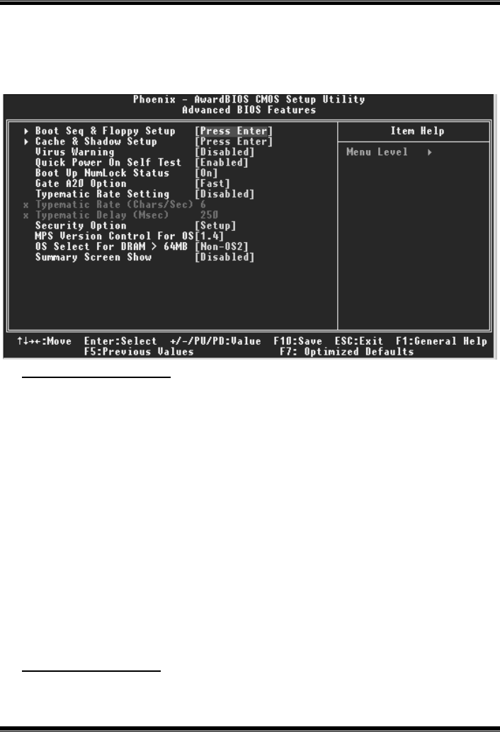
3 Advanced BIOS Features
Figure 3. Adva nced BIOS Se tup
Boot Seq & Floppy Setup
This item allows you to setup boot seq & Floppy.
First/ Second/ Third/ Boot Other Device
These BIOS attempt to load the operating system from the devices in the
sequence selected in these items.
The Choices: Floppy, LS120, HDD-0, SCSI, CDROM, HDD-1, HDD-2, HDD-3,
ZIP100, LAN, Disabled.
Swap Floppy Drive
For systems with two floppy drives, this option allows you to swap logical drive
assignments.
The Choices: Disabled (default), Enabled.
Boot Up Floppy Seek
Enabling this option will test the floppy drives to determine if they have 40 or 80
tracks. Disabling this option reduces the time it takes to boot-up.
The Choices: Enabled (default), Disabled.
Cache & Shadow Setup
This item allows you to setup cache & shadow setup.

M7VIG 400 BIOS Setup
10
CPU Internal Cache
Depending on the CPU/chipset in use, you may be able to increase memory
access time with this option.
Enabled (default) Enable cache.
Disabled Disable cache.
External Cache
This option enables or disables “Level 2” secondary cache on the CPU, which
may improve performance.
Enabled (default) Enable cache.
Disabled Disable cache.
CPU L2 Cache ECC Checking
T his item allows you to enable/disab le CP U L2 Cache ECC Checking.
The Choices: Enabled (default), Disabled.
Video BIOS Shadow
Determines whether video BIOS will be copied to RAM for faster execution.
Enabled (default) Optional ROM is enabled.
Disabled Optional ROM is disabled.
Virus Warning
T his option allows you to choose the Virus Warnin g feature that is used to protect the IDE
Hard Disk boot sector. If this function is enabled and an attempt is made to write to the
boot sector, BIOS will display a warning message on the screen and sound an alarm beep.
Disabled (default) Virus protection is disabled.
Enabled Virus protection is activated.
Quick Power On Self Test
Enabling this option will cause an abridged version of the Power On Self-Test (POST) to
execute after you power up the computer.
Enabled (default) Enable quick POST.
Disabled Normal POST.
Boot Up NumLock Sta tus
Selects the NumLock. State after power on.
On (default) Numpad is number keys.
Off Numpad is arrow keys.
Gate A20 Option
Select if chipset or keyboard controller should control Gate A20.
Normal A pin in the keyboard controller
controls Gate A20.
Fast (default) Lets chipset control Gate A20.

M7VIG 400 BIOS Setup
11
Typematic Rate Setting
When a key is held down, the keystroke will repeat at a rate determined by the keyboard
controller. When enabled, the typematic rate and typematic delay can be configured.
Disabled (default)
Enabled
Typematic Rate (Chars/Sec)
Sets the rate at which a keystroke is repeated when you hold the key down.
The Choices: 6 (default), 8,10,12,15,20,24,30.
Typematic Delay (Msec)
Sets the delay time after the key is held down before it begins to repeat the keystroke.
The Choices: 250 (default), 500,750,1000.
Security Option
This option will enable only individuals with passwords to bring the system online and/or
to use the CMOS Setup Utility.
System A password is required for the system to boot and is
also required to access the Setup Utility.
Setup (default) A password is required to access the Setup Utility
only.
This will only apply if passwords are set from the Setup main menu.
MPS Version Control For OS
The BIOS supports version 1.1 and 1.4 of the Intel multiprocessor specification.
Select version supported by the operation system running on this computer.
The Choices: 1.4 (default), 1.1.
OS Select For DRAM > 64MB
A choice other than Non-OS2 is only used for OS2 systems with memory exceeding 64MB.
The Choices: Non-OS2 (default), OS2.
Summary Screen Show
This item allows you to enable/ disable display the Summary Screen Show.
The Choices: Disabled (default), Enabled.
M7VIG 400 BIOS Setup
12
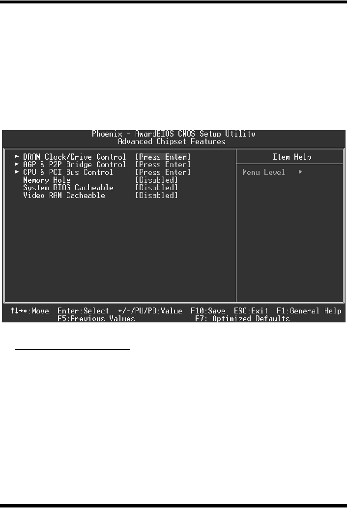
4 Advanced Chipset Features
This submenu allows you to configure the specific features of the chipset installed on your
system. This chipset manage bus speeds and access to system memory resources, such as
DRAM. It also coordinates communications with the PCI bus. The default settings that came
with your system have been optimized and therefore should not be changed unless you are
suspicious that the settings have been changed incorrectly.
Fig ure 4. Advance d Chipse t Setup
DRAM Clock/Drive Control
To control the Clock/Drive. If you highlight the literal “Press Enter” next to the “DRAM
Clock/Drive Control” label and then press the enter key, it will take you a submenu with
the followin g options :
DRAM Clock
This item determines DRAM clock following 100MHz, 133MHz, 166MHz or By
SPD.
The Choices: 100MHz, 133MHz, By SPD (default), 166MHz.

M7VIG 400 BIOS Setup
13
DRAM Timing
This item determines DRAM clock/ timing follow SPD or not.
The Choices: Auto By SPD (default), Manual, Turbo, Ultra.
DRAM CAS Latency
When DRAM is installed, the number of clock cycles of CAS latency depends on
the DRAM timing.
The Choices: 2.5 (default), 2.
Bank Interleave
This item allows you to enable or disable the bank interleave feature.
The Choices: Disabled (default), 2 bank, 4 bank.
Precharge to Active (Trp)
This items allows you to specify the delay from precharge command to activate
command.
The Choices: 2T, 3T, 4T, 5T (default).
Tras Non DDR 400/ DDR 400
This item allows you to choose Non DDR 400/ DDR 400
The Choices: 6T/ 8T, 7T/10T (default), 5T / 6T , 8T , 12T .
Active to Precharge (Tras)
This items allows you to specify the minimum bank active time.
The Choices: 7T, 6T (default).
Active to CMD (Trcd)
Use this item to specify the delay from the activation of a bank to the time that a
read or write command is accepted.
The Choices: 2T, 3T, 4T, 5T (default).
DRAM Burst Length
This item allows you to place the length of the memory.
The Choices: 4 (default), 8.
DRAM Queue Depth
This item permits to place the depths of the memory. The deeper the depth is,
the better is this function.
The Choices: 4 level (default), 2 level, 3 leve l.
DRAM Command Rate
This item controls clock cycle that must occur between the last valid write
operation and the next command.
The Choices: 1T Command, 2T Co mmand (default).
Write Recovery Time
This item allows you to select the recovery time.

M7VIG 400 BIOS Setup
14
The Choices: 2T, 3T (default).
tWTR for DDR400 only
This item allows you to choose tWTR for DDR 400 only.
The Choices: 1T, 2T, 3T (default).
AGP & P2P Bridge Control
If you highlight the literal “Press Enter” next to the “AGP & P2P Bridge Control” label and
then press the enter key, it will take you a submenu with the follow in g options :
AGP Aperture Size
Select the size of the Accelerated Graphics Port (AGP) aperture. The aperture is
a portion of the PCI memory address range dedicated for graphics memory
address space. Host cycles that hit the aperture range are forwarded to the AGP
without any translation.
The Choices: 64M, 256M, 128M (default), 32M, 16M, 8M, 4M.
AGP Mode
This item allows you to select the AGP Mode.
The Choices: 4X (default), 2X, 1X.
AGP Driving Control
By choosing “Auto” the system BIOS will the AGP output Buffer Drive strength
P Ctrl by AGP Card. By choosing “Manual”, it allows user to set AGP output
Buffer Drive strength P Ctrl by manual.
The Choices: Auto (default), Manual.
AGP Driving Value
While AGP driving control item set to “Manual”, it allows user to set AGP
driving.
The Choices: DA (default).
AGP Fast Write
This item allows you to enable or disable AGP Fast Write function.
The Choices: Enabled, Disabled (default).
AGP Master 1 WS Write
When Enabled, writes to the AGP (Accelerated Graphics Port) are executed with
one-wait states.
The Choices: Disabled (default), Enabled.
AGP Master 1 WS Write
When Enabled, write to the AGP (Accelerated Graphics Port) are executed with
one wait states.
The Choices: Disabled (default), Enabled.
AGP Master 1 WS Read
When Enabled, read to the AGP (Accelerated Graphics Port) are executed with

M7VIG 400 BIOS Setup
15
one wait states.
The Choices: Disabled (default), Enabled.
CPU & PCI Bus Control
If you highlight the literal “Press Enter” next to the “CPU & PCI Bus Control” label and
then press the enter key, it will take you a submenu with the follow in g options :
PCI1 Master 0 WS Write
When enabled, writes to the PCI bus are executed with zero-wait states.
The Choices: Enabled (default), Disabled.
PCI2 Master 0 WS Write
When enabled, writes to the AGP bus are executed with zero-wait states.
The Choices: Enabled (default), Disabled.
PCI1 Po st Write
When Enabled, CPU writes are allowed to post on the PCI bus.
The Choices: Enabled (default), Disabled.
PCI2 Po st Write
When Enabled, CPU writes are allowed to post on the AGP bus.
The Choices: Enabled (default), Disabled.
VLink 8X Support
This item allows you to enable or disable VLink 8X support.
The Choices: Enabled (default), Disabled.
PCI Delay Transaction
The chipset has an embedded 32-bit posted write buffer to support delay
transactions cycles. Select Enabled to support compliance with PCI specification.
The Choices: Enabled (default), Disabled.
Memory Hole
When enabled, you can reserve an area of system memory for ISA adapter ROM. When
this area is reserved, it cannot be cached. Refer to the user documentation of the peripheral
you are installing for more information.
The Choices: Disabled (default), 15M – 16M.
System BIOS Cacheable
Selecting the “Enabled” option allows caching of the system BIOS ROM at
F0000h-FFFFFh, which can improve system performance. However, any programs writing
to this area of memory will cause conflicts and result in system errors.
The Choices: Enabled, Disabled (default).
Video RAM Cacheable
Enabling this option allows caching of the video RAM, resulting in better system
performance. However, if any program writes to this memory area, a system error may
result.
The Choices: Enabled, Disabled (default).
M7VIG 400 BIOS Setup
16
5 Integrated Peripherals
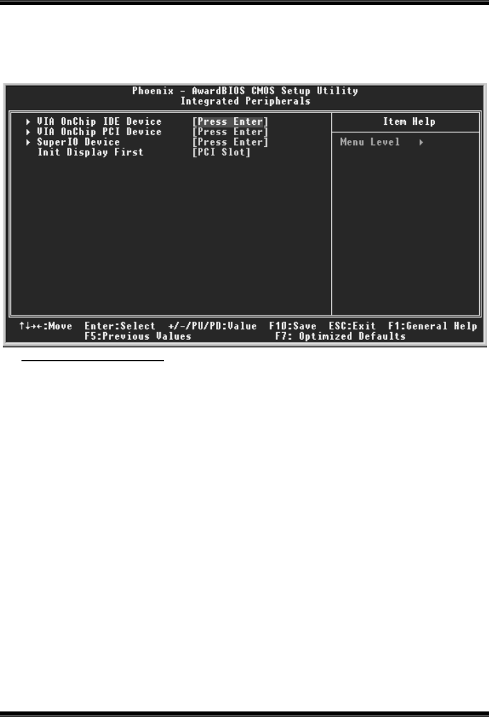
Figure 5. Integrated Peripherals
VIA OnChip IDE Device
The chipset contains a PCI IDE interface with support for two IDE channels.
Select “Enabled” to activate the first and / or second IDE interface. If you install a primary
and / or secondary add-in IDE interface, select “Disabled” to deactivate an interface. If you
high light the litera l “P ress Enter” next to the “Onchip IDE Control” labe l and then press the
enter key, it will take you a submenu with the following options:
OnChip SATA
This item allows you to enable or disable the On-Chip Serial ATA.
The Choices: Enabled (default), Disabled.
IDE DMA transfer access
The “onboard” IDE drive interface supports IDE DMA read/write function.
The Choices: Enabled (default), Disabled.
OnChip IDE Channel 0/1
The motherboard chipset contains a PCI IDE interface with support for
two IDE channels. Select “Enabled” to activate the first and/or second IDE
interface. Select “Disabled” to deactivate an interface if you are going to install a
primary and/or secondary add-in IDE interface.
The Choices: Enabled (default), Disabled.

M7VIG 400 BIOS Setup
17
IDE Prefetch Mode
The “onboard” IDE drive interfaces supports IDE prefetching for faster drive
access. If the interface does not support prefetching. If you install a primary
and/or secondary add-in IDE interface, set this option to “Disabled”.
The Choices: Enabled (default), Disabled.
Primary / Secondary Master / Slave PIO
The IDE PIO (Programmed Input / Output) fields let you set a PIO mode (0-4)
for each of the IDE devices that the onboard IDE interface supports. Modes 0
through 4 provides successively increased performance. In Auto mode, the
system automatically determines the best mode for each device.
The Choices: Auto (default), Mode0, Mode1, Mode2, Mode3, Mode4.
Primary / Secondary Master / Slave UDMA
Ultra DMA/100 functionality can be implemented if it is supported by the IDE
hard drives in your system. As well, your operating environment requires a DMA
driver (Windows 95 OSR2 or a third party IDE bus master driver). If your hard
drive and your system software both support Ultra DMA/100, select Auto to
enable BIOS support.
The Choices: Auto (default), Disabled.
IDE HDD Block Mode
If your IDE hard drive supports block mode, select “Enabled” for automatic
detection of the optimal number of block read/ writes per sector the drive can
support.
The Choices: Enabled (default), Disabled.
VIA OnChip PCI Device
If you highlight the literal “Press Enter” next to the “OnChip PCI Device” labe l and then
press the enter key, it will take you a submenu with the following options:
VIA-3058 AC97 Audio
This option allows you to control the onboard AC97 audio.
The Choices: Auto (default), Disabled.
VIA-3068 MC97 Modem
This option allows you to control the onboard MC97 modem.
The Choices: Auto (default), Disabled.
VIA-3043 OnChip LAN
This option allows you to control the onboard LAN.
The Choices: Enabled (default), Disabled.
Onboard LAN Boot ROM
This item allows you to enable or disable Onboard LAN Boot ROM.
The Choices: Disabled (default), Enabled.

M7VIG 400 BIOS Setup
18
Onchip USB Co ntro ller
Select “Enabled” if your system contains a Universal Serial Bus (USB) controller
and you have USB peripherals.
The Choices: All Enabled (default), All Disab led.
Onchip EHCI Controller
This item allows you to enable or disable the Onchip EHCI controller.
The Ch o i ce s : En a b le d (default), Disabled.
USB Keyboard/ Mouse Support
This item allows you to enable or disable the USB Keyboard/ Mouse Legacy
Support.
The Choices: Disabled (default), Enabled.
1394 Fire Wire
This item allows you to enable or disable 1394 Fire Wire.
The Choices: Enabled (default), Disabled.
Super IO Device
If you highlight the literal “Press Enter” next to the “Super IO Device” labe l and then
press the enter key, it will take you a submenu with the following options:
Onboard FDC Controller
Select Enabled if your system has a floppy disk controller (FDC) installed on the
system board and you wish to use it. If install and FDC or the system has no
floppy drive, select Disabled in this field.
The Choices: Enabled (default), Disabled.
Onboard Serial Port 1
Select an address and corresponding interrupt for the first and second serial ports.
The Choices: Disabled, 3F8/IRQ4 (default), 2F8/IRQ3, 3E8/IRQ4, 2E8/IRQ3,
Auto.
Onboard Serial Port 2
Select an address and corresponding interrupt for the first and second serial ports.
The Choices: Disabled (default), 2F8/IRQ3, 3F8/IRQ4, 3E8/IRQ4,
2E8/IRQ3, Auto.
UART Mode Select
This item allows you to determine which Infra Red (IR) function of onboard I/O
chip.
The Choices: Normal, AS KIR, IrDA (default).
RxD, TxD Active
This item allows you to determine which Infrared (IR) function of onboard I/O
chip.
The Choices: Hi / Lo (default), Hi / Hi, Lo / Hi, Lo / Lo.

M7VIG 400 BIOS Setup
19
IR Transmission Delay
T his item allows you to enable/disab le IR transmission de lay.
The Choices: Enabled (default), Disabled.
UR2 Duplex Mode
Select the value required by the IR device connected to the IR port. Full-duplex
mode permits simultaneous two-direction transmission. Half-duplex mode
permits transmission in one direction only at a time.
The Choices: Half (default), Full.
Use IR Pins
Consult your IR peripheral documentation to select the correct setting of the TxD
and RxD signals.
The Choices: IR-Rx2Tx2 (default), RxD2, TxD2.
Onboard Parallel Port
This item allows you to determine access onboard parallel port controller with
which I/O Address.
The Choices: 378/IRQ7 (default), 278/IRQ5, 3BC/IRQ7, Disabled.
Parallel Port Mode
The default value is SPP.
The Choices:
SPP(default) Using Parallel port as Standard Printer Port.
EPP Usin g P aralle l Port as Enhanced P aralle l P ort.
ECP Usin g P aralle l port as Extended Capabilities Port.
ECP+EPP Usin g P aralle l port as ECP & EPP mode.
EPP Mode Select
Select EPP port type 1.7 or 1.9.
The Choices: EPP 1.7(default), EPP1.9.
ECP Mode Use DMA
Select a DMA Channel for the port.
The Choices: 3 (default), 1.
Game Port Address
Game Port I/O Address.
The Choices: 201 (default), 209, Disabled.
Midi Port Address
Midi Port Base I/O Address.
The Choices: 330 (default), 300, 290, Disabled.
Midi Port IRQ
This determines the IRQ in which the Midi Port can use.

M7VIG 400 BIOS Setup
20
The Choices: 5, 10 (default)
Init Display First
With systems that have multiple video cards, this option determines whether the primary
display uses a PCI Slot or an AGP Slot.
The Choices: PCI Slot (default), AGP.
M7VIG 400 BIOS Setup
21
6 Power Management Setup
The Power Management Setup Menu allows you to configure your system to utilize energy
conservation and power up/power down features.
Figure 6. Power Management Setup
ACPI functio n
This item displays the status of the Advanced Configuration and Power Management
(ACPI).
The Choices: Enabled (default), Disabled.
ACPI Sus pend Type
The item allows you to select the suspend type under the ACPI operating system.
The Choices: S1 (POS) (default) Power on Suspend
S3 (STR) Suspend to RAM
S1+S3 POS+STR
Power Management
This category allows you to select the type (or degree) of power saving and is directly
related to the following modes:
1.HDD Power Down.
2.Suspend Mode.

M7VIG 400 BIOS Setup
22
There are four options of Power Management, three of which have fixed mode settings
Min. Power Saving
Minimum power management.
Suspend Mode = 1 hr.
HDD Power Down = 15 min
Max. Power Saving
Maximum power management only available for sl CPU’s.
Suspend Mode = 1 min.
HDD Power Down = 1 min.
User De fine (default)
Allows you to set each mode individually.
When not disabled, each of the ranges are from 1 min. to 1 hr. except for HDD
Power Down which ranges from 1 min. to 15 min. and disable.
HDD Power Down
When enabled, the hard disk drive will power down and after a set time of system inactivity.
All other devices remain act ive.
The Choices: Disabled (default), 1 Min, 2 Min, 3 Min, 4 Min, 5 Min, 6 Min, 7 Min, 8 Min,
9 Min, 10 Min, 11 Min, 12 Min, 13 Min, 14 Min, 15Min.
Suspend Mode
The item allows you to select the suspend type under ACPI operating system.
The Choices: Disabled (default), 1 Min, 2 Min, 4 Min, 6 Min, 8 Min, 10 Min, 20 Min, 30
Min, 40 Min, 1 Hour.
Video Off Option
This field determines when to activate the video off feature for monitor power
management.
The Choices: Suspend→Off (default), Always on.
Video Off Method
T his option determines the manner in which the monitor is goes blank.
V/H SYNC+Blank (default)
This selection will cause the system to turn off the vertical and horizontal
synchronization ports and write blanks to the video buffer.
Blank Screen
This option only writes blanks to the video buffer.
DPMS

M7VIG 400 BIOS Setup
23
Initial disp lay power management signa lin g.
The Choices: Stop Grant, PwrOn Suspend.
Modem Use IRQ
This determines the IRQ, which can be applied in MODEM use.
The Choices: 3 (default),4 / 5 / 7 / 9 / 10 / 11 / NA.
Run VGABIOS if S3 Resume
Choosing Enabled will make BIOS run VG A BIOS to in itialize the VGA card when system
wakes up from S3 state . The system time is shortened if you disable the function , but
system will need AGP driver to init ialize the card . So , if the AGP driver of the VGA card
does not support the initialization feature , the display may work abnormally or not function
after S3 .
The Choices:Au t o , Yes (default), No.
Soft-Off by PWRBTN
Pressing the power button for more than 4 seconds forces the system to enter the
Soft-Off state when the system has “hung.”
The Choices: Delay 4 Sec, Instant-Off (default).
PWRON After PWR-Fail
This field determines the action the system will automatically take when power is
restored to a system that had lost power previously without any subsequent
manual intervention. There are 3 sources that provide current to the CMOS area
that retains these Power-On instructions; the motherboard battery (3V), the Power
Supply (5VSB), and the Power Supply (3.3V). While AC is not supplying power,
the motherboard uses the motherboard battery (3V). If AC power is supplied and
the Power Supply is not turned on, 5VSB from the Power Supply is used. When
the Power Supply is eventually turned on 3.3V from the Power Supply will be
used.
There are 3 options: “Former-Sts”, “On”, “Off”.
“Former-Sts” Means to maintain the last status of the CMOS when AC
power is lost.
“On” Means always set CMOS to the “On” status when AC
power is lost
“Off” (default) Means always set CMOS to the “Off” status when AC
power is lost.
For example: If set to “Former-Sts” and AC power is lost when system is live,
then after AC power is restored, the system will automatically power on. If AC
power is lost when system is not live, system will remain powered off.
IRQ/Event Activity Detect

M7VIG 400 BIOS Setup
24
If you highlight the literal “Press Enter” next to the “IRQ/Event Activity Detect” label
and then press the enter key, it will take you a submenu with the following options:
PS2KB Wakeup Select
When select password, please press Enter key to change password Max 8
numbers.
The Choices: Hot Key (default)
PS2KB Wakeup from S3/S4/S5
When select password, please press Enter key to change password with a
maximum of 8 numbers.
The Choices: Wake (default), Power, Ctrl+F7, Ctrl+F8, Ctrl+F9, Ctrl+F10,
Ctrl+F11, Ctrl+F12.
USB Resume from S3
This item allows you to disable /enable USB resume from S3.
The Choices: Disable (default), Enable.
VGA
When set to On, any event occurring at a VGA Port will awaken a system which
has been powered down.
The Choices: Off (default), On.
LPT & COM
When this option is set to On, any event occurring at a COM(serial)/LPT (printer)
port will awaken a system which has been powered down.
The Choices: LPT/COM (default), COM, LPT, NONE.
HDD & FDD
When this option is set to On, any event occurring on a hard drive or a floppy
drive will awaken a system which has been powered down.
The Choices: On (default), Off.
PCI Master
When set to On, you need a LAN add-on card which supports the power function.
It should also support the wake-up on LAN jump.
The Choices: Off (default), On.
PowerOn by PCI Card
When you select Enabled, a PME signal from PCI card returns the system to Full
ON state.
The Choices: Disabled (default), Enabled.
Wake Up On LAN/Ring
To use this function, you need a LAN add-on card which support power on
function. It should also support the wake-up on LAN jump.
Disabled (default) Wake up on LAN/Ring not supported.
Enabled Wake up on LAN/Ring supported.

M7VIG 400 BIOS Setup
25
RTC Alarm Resume
When “Enabled”, you can set the date and time at which the RTC (real-time
clock) alarm awakens the system from Suspend mode.
The Choices: Enabled, Disabled (default).
IRQs Activity Monitoring
Press Enter to access another sub menu used to configure the different wake up
events (i.e. wake on LPT & COMM activity).
Primary INTR On
IRQ3 (COM2) Enabled
IRQ4 (COM1) Enabled
IRQ5 (LPT2) Enabled
IRQ6 (Floppy Disk) Enabled
IRQ7 (LPT1) Enabled
IRQ8 (RTC Alarm) Disabled
IRQ9 (IRQ2 Redir) Disabled
IRQ10 (Reserved) Disabled
IRQ11 (Reserved) Disabled
IRQ12 (PS/2 Mouse) Enabled
IRQ13 (Coprocessor) Enabled
IRQ14 (Hard Disk) Enabled
IRQ15 (Reserved) Disabled
M7VIG 400 BIOS Setup
26
7 PnP/PCI Configurations
This section describes configuring the PCI bus system. PCI, or Personal Computer
Interconnect, is a system which allows I/O devices to operate at speeds nearing the speed of
the CPU itself uses when communicating with its own special components. This section
covers some very technical items and it is strongly recommended that only experienced
users should make any changes to the default settings.
Figure 7. PnP/PCI Configurations
PNP OS Installed
When set to YES, BIOS will only in itialize the P nP cards used for the boot sequence (VGA,
IDE, SCSI). The rest of the cards will be initialized by the PnP operating system like
Window™ 95. When set to NO, BIOS will init ia lize a ll the P nP cards. For non-P nP
operating systems (DOS, Netware™), this option must set to NO.
The Choices: No (default), Yes.
Reset Configuration Data
The system BIOS supports the PnP feature which requires the system to record which
resources are assigned and protects resources from conflict. Every peripheral device has a
node, which is called ESCD. This node records which resources are assigned to it. The
system needs to record and update ESCD to the memory locations. T hese locations (4K)
are reserved in the system BIOS. If the Disabled (default) option is chosen, the system‘s
ESCD will update only when the new configuration varies from the last one. If the Enabled

M7VIG 400 BIOS Setup
27
option is chosen, the system is forced to update ESCDs and then is automatically set to the
“Disab led” mode.
The above settings will be shown on the screen only if “Manual” is chosen for the resources
controlled by function.
Legacy is the term, which signifies that a resource is assigned to the ISA Bus and provides
non-PnP ISA add-on cards. PCI / ISA PnP signifies that a resource is assigned to the PCI
Bus or provides for ISA PnP add-on cards and peripherals.
The Choices: Disabled (default), Enabled.
Resources Controlled By
By Choosing “Auto(ESCD)” (default), the system BIOS will detect the system resources
and automatically assign the relative IRQ and DMA channel for each peripheral.By
Choosing “Manual”, the user will need to assign IRQ & DMA for add-on cards. Be sure
that there are no IRQ/DMA and I/O port conflicts.
IRQ Resources
This submenu will allow you to assign each system interrupt a type, depending on the type
of device using the interrupt. When you press the “Press Enter” tag, you will be directed to
a submenu that will allow you to configure the system interrupts. This is only
configurable when “Resources Controlled By” is set to “Manual”.
IRQ-3 assigned to PCI Device
IRQ-4 assigned to PCI Device
IRQ-5 assigned to PCI Device
IRQ-7 assigned to PCI Device
IRQ-9 assigned to PCI Device
IRQ-10 assigned to PCI Device
IRQ-11 assigned to PCI Device
IRQ-12 assigned to PCI Device
IRQ-14 assigned to PCI Device
IRQ-15 assigned to PCI Device
PCI / VGA Palette Snoop
Choose Disabled or Enabled. Some graphic controllers which are not VGA compatible
take the output from a VGA controller and map it to their display as a way to provide boot
information and VGA compatibility.
However, the color information coming from the VGA contro ller is drawn from the palette
table inside the VGA controller to generate the proper colors, and the graphic controller
needs to know what is in the palette of the VGA controller. To do this, the non-VGA
graphic controller watches for the Write access to the VGA palette and registers the snoop
data. In PCI based systems, where the VGA controller is on the PCI bus and a non-VGA
graphic controller is on an ISA bus, the Write Access to the palette will not show up on the
ISA bus if the PCI VGA controller responds to the Write.

M7VIG 400 BIOS Setup
28
In this case, the P CI VGA controller shou ld not respond to the Write, it should only snoop
the data and permit the access to be forwarded to the ISA bus. The non-VGA ISA graphic
controller can then snoop the data on the ISA bus. Unless you have the above situation,
you should disable this option.
Disabled (default) Disables the function.
Enabled Enables the function.
Assign IRQ For VGA
This item allows the users to choose which IRQ to assign for the VGA.
The Choices: Enabled (default), Disabled.
Assign IRQ For USB
This item allows the users to choose which IRQ to assign for the USB.
The Choices: Enabled (default), Disabled.
M7VIG 400 BIOS Setup
29
8 PC Health Status
Figure 8. PC Health Status
Current CPU1 Temperature
This field displays the current temperature of the CPU.
Current CPU FAN Speed
This field displays the current speed of CPU fan.
Current SYS FAN Speed
This field displays the current speed SYSTEM fan.
Shutdown Temperature
T his item allows you to set up the CPU shutdown T emperature. T his item only effective
under Windows 98 ACPI mode.
The Choices: Disabled (default), 60℃/140F, 65℃/149F, 70℃/158F, 75℃/167F.
CPU Vcore/ 3.3V/ +5V/ +12V/ -12V/ -5V/ 5VSB/ VBAT(V)
Detect the system’s voltage status automatically.

M7VIG 400 BIOS Setup
30
Show H/W Monitor in POST
If your computer contains a monitoring system, it will show PC health status during POST
stage. The item offers several delay time for you to choose.
The Choices: Enabled (default), Disabled.
Chassis Open Warning
This item allows you to enable or disable Chassis Open Warning beep.
The Choices: Disabled (Default), Enabled.
M7VIG 400 BIOS Setup
31
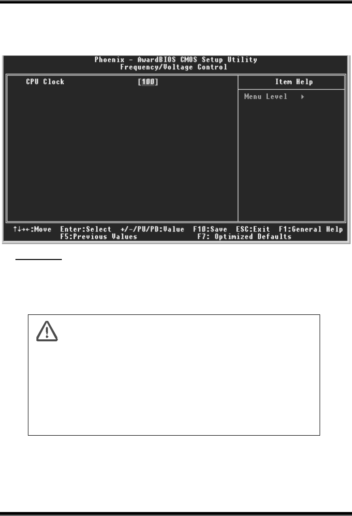
9 Frequency/ Voltage Control
Fig ure 9. Frequency/ Voltage Co ntro l
CPU Clock
This item allows you to select CPU Clock, and CPU over clocking.
The Choices: 100MHz (Default)
Min = 100 Max = 132
Key in a Dec Number.
If unfortunately, the system’s frequency that you are selected is
not functioning, there are two methods of booting-up the system.
Method 1: Clear the COMS data by setting the JCOMS1 ((2-3) closed))
as “ON” status. All the CMOS data will be loaded as
defaults setting.
Method 2: Press the <Insert> key and Power button simultaneously,
after that keep-on pressing the <Insert> key until the
power-on screen showed. This action will boot-up the
system according to FSB of the processor.
※ It’s strongly recommended to set CPU Vcore and clock in
default setting. If the CPU Vcore and clock are not in default
setting, it may cause CPU or M/B damage.
