Bird Technologies Group 5PI613805 SIGNAL BOOSTER User Manual 9408cvr 1 2
Bird Technologies Group SIGNAL BOOSTER 9408cvr 1 2
USERS MANUAL

Part No.
61-38-05 UserMan page 1 of 38
Installation and Operation Manual
for the Two-Way Signal Booster System
Model Number 61-38-05
First Printing: June 2005
7-9408-1.2
Version Number Version Date
1 06/14/05
1.1 07/12/05
1.2 07/25/05
Copyright © 2005 TX RX Systems Inc.
61-38-05 UserMan page 2 of 38
NOTE
WARNING
Warranty
This warranty applies for one year from shipping date.
TX RX Systems Inc. warrants its products to be free from defect in material and workman-
ship at the time of shipment. Our obligation under warranty is limited to replacement or
repair, at our option, of any such products that shall have been defective at the time of
manufacture.
TX RX Systems Inc. reserves the right to replace with merchandise of equal performance
although not identical in every way to that originally sold.
TX RX Systems Inc. is not liable for damage caused by lightning or other natural disasters.
No product will be accepted for repair or replacement without our prior written approval.
The purchaser must prepay all shipping charges on returned products. TX RX Systems
Inc. shall in no event be liable for consequential damages, installation costs or expense of
any nature resulting from the purchase or use of products, whether or not they are used in
accordance with instructions. This warranty is in lieu of all other warranties, either ex-
pressed or implied, including any implied warranty or merchantability of fitness. No repre-
sentative is authorized to assume for TX RX Systems Inc. any other liability or warranty
than set forth above in connection with our products or services.
Terms and Conditions of Sale
PRICES AND TERMS: Prices are FOB seller’s plant in Angola, NY domestic packaging
only, and are subject to change without notice. Federal, State and local sales or excise
taxes are not included in prices. When Net 30 terms are applicable, payment is due
within 30 days of invoice date. All orders are subject to a $100.00 net minimum.
QUOTATIONS: Only written quotations are valid.
ACCEPTANCE OF ORDERS: Acceptance of orders is valid only when so acknowledged
in writing by the seller.
SHIPPING: Unless otherwise agreed at the time the order is placed, seller reserves the
right to make partial shipments for which payment shall be made in accordance with
seller’s stated terms. Shipments are made with transportation charges collect unless
otherwise specified by the buyer. Seller’s best judgement will be used in routing, except
that buyer’s routing is used where practicable. The seller is not responsible for selection
of most economical or timeliest routing.
CLAIMS: All claims for damage or loss in transit must be made promptly by the buyer
against the carrier. All claims for shortages must be made within 30 days after date of
shipment of material from the seller’s plant.
SPECIFICATION CHANGES OR MODIFICATIONS: All designs and specifications of
seller’s products are subject to change without notice provided the changes or modifi-
cations do not affect performance.
RETURN MATERIAL: Product or material may be returned for credit only after written
authorization from the seller, as to which seller shall have sole discretion. In the event
of such authorization, credit given shall not exceed 80 percent of the original purchase.
In no case will Seller authorize return of material more than 90 days after shipment from
Seller’s plant. Credit for returned material is issued by the Seller only to the original
purchaser.
ORDER CANCELLATION OR ALTERATION: Cancellation or alteration of acknowledged
orders by the buyer will be accepted only on terms that protect the seller against loss.
NON WARRANTY REPAIRS AND RETURN WORK: Consult seller’s plant for pricing.
Buyer must prepay all transportation charges to seller’s plant. Standard shipping policy
set forth above shall apply with respect to return shipment from TX RX Systems Inc. to
buyer.
Disclaimer
Product part numbering in photographs and drawings is accurate at time of printing.
Part number labels on TX RX products supercede part numbers given within this manual.
Information is subject to change without notice.
Symbols
Commonly Used
CAUTION or
ATTENTION
High Voltage
Use Safety
Glasses
ESD
Electrostatic
Discharge
Hot Surface
Electrical Shock
Hazard
Important
Information
61-38-05 UserMan page 3 of 38
To satisfy FCC RF exposure requirements for transmitting
devices, a separation distance of 70 Centimeters or more
should be maintained between the UPLINK antenna of this
device and persons during device operation. To satisfy FCC
RF exposure requirements for transmitting devices, a sepa-
ration distance of 21.5 Centimeters or more should be main-
tained between the DOWNLINK antenna of this device and
persons during device operation. To ensure compliance,
operations at closer than these distances is not recom-
mended.
The antenna used for this transmitter must not be co-located
in conjunction with any other antenna or transmitter.
WARNING
For Class A Unintentional Radiators
This equipment has been tested and found to comply with the limits for a Class A digital device, pursuant to
part 15 of the FCC rules. These limits are designed to provide reasonable protection against harmful inter-
ference when the equipment is operated in a commercial environment. This equipment generates, uses,
and can radiate radio frequency energy and, if not installed and used in accordance with the instruction
manual, may cause harmful interference to radio communications. Operation of this equipment in a resi-
dential area is likely to cause harmful interference in which case the user will be required to correct the
interference at his own expense.
Changes or modifications not expressly approved by TX
RX System Inc. could void the user’s authority to operate
the equipment.
WARNING
This device complies with Part 15 of the FCC Rules. Operation is subject to the
following two conditions: (1) this device may not cause harmful interference and
(2) this device must accept any interference received, including interference
that may cause undesired operation.
61-38-05 UserMan page 4 of 38
Antenna System Installation
The antenna or signal distribution system consists of two branches. An uplink
branch typically uses an outdoor mounted, unidirectional gain antenna such
as a yagi and a downlink signal radiating system consisting of a network of
zero-gain whip antennas or lengths of radiating cable usually mounted inside
of the structure.
Even though the antenna system may not be supplied or installed by TX RX
Systems. The following points need to be observed because both the safety
of the user and proper system performance depend on them.
1) Antenna system installation should only be performed by qualified techni-
cal personnel.
2) The following instructions for your safety describe antenna installation
guidelines based on FCC Maximum RF Exposure Compliance require-
ments.
3) The uplink antenna is usually mounted outside and exchanges signals
with the repeater base station or donor site. It is typically mounted perma-
nently-attached to the building wall or roof. The gain of this antenna should
NOT exceed 10 dB. Only qualified personnel should have access to the
antenna and under normal operating conditions, no one should be able to
touch or approach it within 70 Centimeters (28 inches).
4) The downlink or in-building signal distribution system is connected to the
downlink booster port using coaxial cable. The distribution system may
use radiating coaxial cable or a network 1/4 wave whip antennas whose
gain does not exceed 0 dB for any radiator. These antennas should be
installed so that the user cannot approach any closer than 21.5 Centime-
ters (9 inches) from the antenna.
Table of Contents Manual 7-9408-1.2 07/25/05
61-38-05 UserMan page 5 of 38
Table of Contents
Section 1
Introduction ......................................................................................................... 1
Note About Output Power Rating ........................................................................ 3
Installation............................................................................................................ 3
Cautionary Notes ................................................................................................. 4
Pre-RF Connection Tests.................................................................................... 4
Test Equipment ................................................................................................... 5
Antenna Isolation ................................................................................................. 5
Procedure for Measuring Antenna Isolation ........................................................ 5
Increasing Isolation.............................................................................................. 6
Input Signal Levels .............................................................................................. 6
Procedure for Measuring Input Signal Levels...................................................... 6
Reduction of Incoming Signal Strength ............................................................... 8
Setting Signal Booster Gain ................................................................................ 8
Gain Reduction Methods ..................................................................................... 8
Bypassing Amplifier Sections ............................................................................ 9
Operation.............................................................................................................. 9
Signal Flow........................................................................................................... 9
System Components.........................................................................................10
Passive Filtering ................................................................................................ 10
DC Regulator (3-5969) ...................................................................................... 11
OLC Assembly (3-6280) .................................................................................... 11
Pre-amplifier Stage (3-11423) ...........................................................................12
Driver Amplifier Stage (3-11423) ....................................................................... 13
Hi Power Amplifier Assembly (3-11792)............................................................13
Signal Sampler (3-6999).................................................................................... 13
Signal Sampler (3-3569).................................................................................... 13
DC Junction Box (3-6254) ................................................................................. 13
Power Supply Assembly (3-15503) ................................................................... 13
Performance Survey.......................................................................................... 14
Field Adjustments ............................................................................................. 14
Filter Tuning....................................................................................................... 15
Helical Preselectors........................................................................................... 16
Required Equipment........................................................................................ 16
Tuning Procedure ............................................................................................ 16
Bandpass Filters................................................................................................ 17
Required Equipment........................................................................................ 17
Tuning Procedure ............................................................................................ 17
Pseudo-Bandpass Filters ..................................................................................18
Required Equipment........................................................................................ 19
Tuning Procedure ............................................................................................ 19
Notch Filters ...................................................................................................... 20
Required Equipment........................................................................................ 20
Tuning Procedure ............................................................................................ 21
Single Section Amplifier Subassemblies ........................................................... 22
Amplifier Tuning...............................................................................................22
Required Equipment........................................................................................ 22
Adjustment Procedure ..................................................................................... 23
Output Level Control (OLC)............................................................................... 25
Checking for Overload.....................................................................................25
Table of Contents Manual 7-9408-1.2 07/25/05
61-38-05 UserMan page 6 of 38
Maintenance and Repair ................................................................................... 26
Recommended Replacement Parts ................................................................. 26
Conversion Chart .............................................................................................. 26
Figures and Tables
Figure 1: Front view of typical 61-38-05 system ................................................... 2
Figure 2: Bottom view of the cabinet enclosure.................................................... 3
Figure 3: Top view of the cabinet enclosure......................................................... 4
Figure 4: Measuring antenna isolation ................................................................. 5
Figure 5: Measuring input signal levels ................................................................ 7
Figure 6: Observing RF power output .................................................................. 8
Figure 7: 1 stg/3 stg amplifier assembly 3-11423................................................. 9
Figure 8: OLC assembly 3-6280......................................................................... 12
Figure 9: Measuring signal booster gain ............................................................ 14
Figure 10: Surveying performance .....................................................................15
Figure 11: Preselector tuning ............................................................................. 16
Figure 12: Observing preselector return loss ..................................................... 17
Figure 13: Bandpass filter tuning........................................................................18
Figure 14: The pseudo-bandpass filter...............................................................18
Figure 15: Tuning for maximum return loss ........................................................19
Figure 16: Tuning for maximun attenuation ........................................................ 20
Figure 17: The notch filter................................................................................... 20
Figure 18: Tuning for maximum return loss ........................................................21
Figure 19: Tuning for maximum attenuation ....................................................... 22
Figure 20: Mechanical layout of single section amplifier ....................................23
Figure 21: Measuring amplifer gain .................................................................... 24
Figure 22: Meqsuring input return loss ...............................................................24
Figure 23: Measuring output return loss ............................................................. 25
Figure 24: Measuring reverse isolation ..............................................................25
Specifications .................................................................................................... 33
Power Conversion Chart................................................................................... 35
Notes................................................................................................................... 38

TXRX Systems Inc. Manual 7-9408-1.2 07/25/05 Page 7
61-38-05 UserMan page 7 of 38
INTRODUCTION
This publication, Instruction Manual 7-9408-1, con-
tains information to support the installation, opera-
tion, and maintenance of the model 61-38-05
signal booster system. Also included in this manual
are the procedures necessary for field adjust-
ments. It is assumed that procedures in this man-
ual will be carried out by a skilled electronics
technician who is familiar with the communications
system. This manual also gives an elementary
explanation of the operation of signal boosters and
signal distribution systems. For a more detailed
discussion of signal booster systems and design
methods, refer to the TX RX Systems Inc. publica-
tion "SEMINAR SUBJECTS" entitled "Repeater
Amplifier Systems: Principles and Applications" (lit-
erature number C2012J94). Contact your TX RX
Systems, sales representative if you wish to order
a copy.
The 61-38-05 booster family is designed to cover
the frequency range of 138 to 174 MHz in two non
contiguous bands, One version covers 138 to 144
MHz for operation in Canada and another version
to cover 148 to 174 MHz. This version is also used
to cover U.S. land-mobile frequencies from 150.8
to 174 MHz. Units for both bands share common
active circuitry but differ in the passive filter units
that duplex the downlink and uplink branches from
a common input or to a common output. Because
signal booster systems are often times subjected
to very demanding environments with extreme con-
ditions of temperature, moisture, dirt and corro-
sives, the system is housed in a high quality
(NEMA style) enclosure. This type of housing
maintains its dimensional stability and appearance
better than other materials. Figure 1 shows a front
view of the unit with the door opened.
The system uses linear RF active amplifiers, filters,
OLC (output level control) circuitry, and DC power
sources to adequately boost the level of the RF sig-
nals. Linear power amplifiers (Class-A) are used in
the amplifier stages of this signal booster system in
contrast to the highly efficient Class-C power
amplifiers used in the output stages of most FM
landmobile transmitters. Linear amplifiers are
biased for a relatively high continuous DC current
drain that does not change with changing RF drive
levels.
Class-A amplifiers generally have the lowest effi-
ciency of the various amplifier types, typically in the
range of 25-33%. They also draw relatively high
current levels on a continuous basis, making heat
dissipation an important factor. Their biggest
advantage is faithful reproduction of the input
waveform which results in the lowest levels of inter-
modulation distortion products (IM) of all the
classes of amplifiers. IM generation is a serious
design consideration when two or more channels
are simultaneously present in the same amplifier
stage.
Preselector filters are used in the system to provide
a number of functions including; reduction of the
level of undesired signals that may enter the sys-
tem and also help suppress any IM products that
may be inadvertently generated. They also pro-
duce a convenient impedance characteristic that
allows multiple branch paths to be tied together to
a common input/output port. This is accomplished
using critical length cables from the filter assem-
blies to a tee junction.
The output level of any signal passing through a
signal booster is determined by the input signal
level, the gain of the booster, and the maximum
output power per carrier rating of the booster. The
high power output stages used in the signal
booster may be damaged by excessive input sig-
nals. An output level control (OLC) circuit is added
to each amplifier chain to protect the amplifiers and
reduce spurious signals. The OLC circuit is
designed to maintain the maximum output level of
the booster during times of excessive input signal
levels.
OLC circuitry actuates when a predetermined max-
imum output level is reached. The output power
level in all OLC branches is sampled, and then fed
to a detector circuit which generates a DC voltage
proportional to the output power level. The DC out-
put of the detector is then applied to a control cir-
cuit which develops a voltage used to control a
variable electronic attenuator. The electronically
controlled attenuator is placed within the amplifier
signal path and reduces the incoming signal by an
amount necessary to keep the power from exceed-
ing the maximum safe level. The gain reduction
range is typically from 5 to 40 dB which is more
than adequate for most real life situations.
OLC circuitry should not be considered a panacea
for a poor system design. One undesirable affect of
OLC is that the signal level of all signals being pro-
cessed by the branch will be reduced when the cir-
cuitry is activated. This means that the
61-38-05 UserMan page 8 of 38
TXRX Systems Inc. Manual 7-9408-1.2 07/25/05 Page 8
Figure 1: Front view of a typical model 61-38-05 signal booster system.
Backup Battery
connects here
Filtering Filtering
Signal
Sampler
3-3569
Signal
Sampler
3-3569
Signal
Sampler
3-6999
Signal
Sampler
3-6999
OLC
Assembly
3-6280
OLC
Assembly
3-6280
1 stg/3 stg
Amplifier
Assembly
3-11423
1 stg/3 stg
Amplifier
Assembly
3-11423
High Power
Amplifier
Assembly
3-11792
High Power
Amplifier
Assembly
3-11792
Regulator
3-5969
Regulator
3-5969
Power Supply
Assembly 3-11503
RF In/Output
Connector RF In/Output
Connector
TXRX Systems Inc. Manual 7-9408-1.2 07/25/05 Page 9
61-38-05 UserMan page 9 of 38
performance of the system is actually decreased
on all other channels within the branch as long as
gain reduction is taking place. This implies that
OLC has been designed to handle short term or
transient overdrive episodes only.
Note About Output Power Rating
A single maximum output power rating does not
apply to broadband signal boosters because the
linear amplifiers (Class A) used in them may have
to process multiple simultaneous signals. Under
these conditions, the questions of power rating
becomes more complex.
When more than one signal is amplified, a number
of spurious signals will also appear in the amplified
output. They are referred to as intermodulation dis-
tortion products, more commonly called I.M. These
spurious products would not be present in a per-
fectly linear amplifier but as in all things, something
short of perfection is realized. The net result is that
the total power out in each signal will be somewhat
less than the single carrier rating in order to main-
tain adequate I.M. performance.
INSTALLATION
The layout of the signal distribution system will be
the prime factor in determining the mounting loca-
tion of the signal booster enclosure. However,
safety and serviceability are also key consider-
ations. The unit should be located where it cannot
be tampered with by unauthorized personnel yet is
easily accessible to service personnel using trou-
ble shooting test equipment such as digital multim-
eters and spectrum analyzers. Also consider the
weight and size of the unit should it become
detached from its mounting surfaces for any rea-
son.
Very little is required to install this signal booster.
The unit should be bolted in its permanent position
using lag bolts or other suitable fasteners. Make
sure there is an unobstructed airflow over the
external heatsinks. Safety and serviceability are
key considerations. The signal booster cabinet will
stay warm during normal operation so in the inter-
est of equipment longevity, avoid locations that will
expose the cabinet to direct sun or areas where the
temperature is continually elevated.
The signal booster is designed to be powered from
120 VAC and a conduit entry box is provided at the
bottom of the enclosure for bringing the AC line into
the cabinet. AC line connections should be made in
accordance with local electrical and building codes.
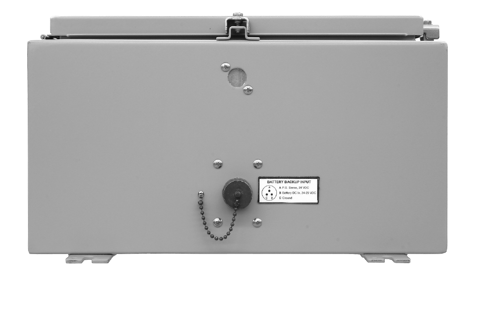
The battery backup system should also be con-
Figure 2: Bottom view of cabinet enclosure.
61-38-05 UserMan page 10 of 38
TXRX Systems Inc. Manual 7-9408-1.2 07/25/05 Page 10
nected at this time. The 3-pin MS style connector
for the backup power system is labeled and is
located on the bottom of the enclosure. A photo-
graph of the bottom of the cabinet is shown in Fig-
ure 2.
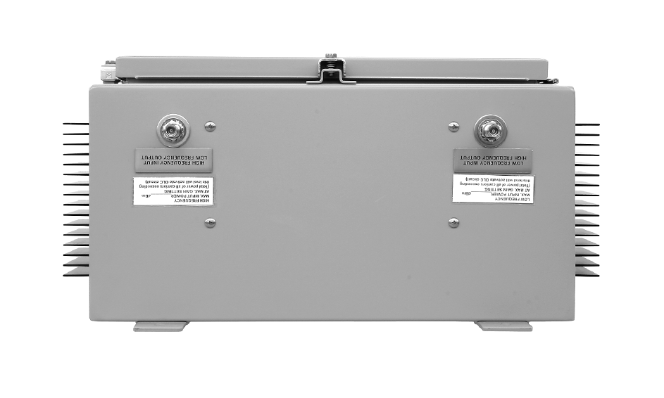
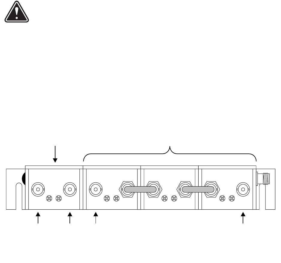
Connection of RF to the unit is made via “N” female
connectors located on top of the cabinet. These
connectors are individually labeled “High Frequen-
cies IN Low frequencies OUT” and “Low Frequen-
cies IN High Frequencies OUT”. Care should be
used when making connections to these ports to
insure the correct antenna cable is connected to its
corresponding input / output port or the system will
not work. The use of high quality connectors with
gold center pins is advised. Flexible jumper cables
made of high quality coax are also acceptable for
connecting to rigid cable sections. A photograph of
the top of the cabinet is shown in Figure 3.
CAUTIONARY NOTES
The following cautions are not intended to frighten
the user but have been added to make you aware
of and help you avoid the areas where experience
has shown us that trouble can occur.
1) Just like the feedback squeal that can occur
when the microphone and speaker get too close to
each other in a public address system, a signal
booster can start to self oscillate. This will occur
when the isolation between the input antenna or
signal source and the output antenna or signal dis-
tribution system does not exceed the signal
booster gain by at least 10 dB. This condition will
reduce the effectiveness of the signal booster and
possibly damage the power amplifier stages.
2) The major cause of damage to signal boosters is
the application of input RF power levels in excess
of the maximum safe input. This can happen inad-
vertently when connecting a signal generator with
full power out to one of the inputs or by a very
strong signal that is far stronger than expected.
The Maximum Safe Power input level for your unit
can be found on the laminated tag affixed to the top
of the cabinet near the RF input/outputs. Following
the pre-installation checks listed below will help to
avoid these two problems.
PRE-RF CONNECTION TESTS
Certain characteristics of the signal distribution
system should be measured before connecting it to
the signal booster. This step is necessary to insure
that no conditions exist that could possibly damage
the signal booster and should not be skipped for
even the most thoroughly designed system. Two
characteristics need to be measured; antenna iso-
lation and input signal levels.
Figure 3: Top view of cabinet enclosure.
TXRX Systems Inc. Manual 7-9408-1.2 07/25/05 Page 11
61-38-05 UserMan page 11 of 38
Test Equipment
The following equipment is required in order to per-
form the pre-installation measurements.
1) Signal generator for the frequencies of interest
capable of a 0 dBm output level. Modulation is
not necessary.
2) Spectrum analyzer that covers the frequencies
of interest and is capable of observing signal
levels down to -100 dBm.
3) Double shielded coaxial test cables made from
RG142 or RG55 coaxial cable.
Antenna Isolation
Antenna isolation is the signal path isolation
between the two sections of the signal distribution
system that are to be connected to the signal
boosters antenna ports. Lack of sufficient isolation
between the input and output antennas can cause
the amplifiers in the system to oscillate. This can
happen at a high enough level to damage the
power amplifier stages. In general, if one or both
antenna ports are connected to sections of radiat-
ing coaxial cable (lossy cable) via short jumpers of
non-radiating cable the isolation will be more than
adequate because of the high coupling loss values
that are encountered with this type of cable. When
a network of antennas are used for the input and
output, this problem is much more likely. Isolation
values are relatively easy to measure with a spec-
trum analyzer and signal generator.
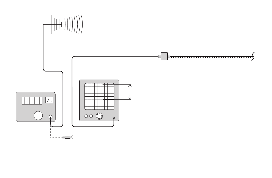
Procedure for Measuring Antenna Isolation
1) Set the signal generator for a 0 dBm output
level at the center frequency of one of the signal
boosters passbands.
2) Set the spectrum analyzer for the same center
frequency and a sweep width equal to or just
slightly greater than the passband chosen in
step one.
3) Connect the test leads of the signal generator
and the spectrum analyzer together using a
female barrel connector, see Figure 4. Observe
the signal on the analyzer and adjust the input
attenuator of the analyzer for a signal level that
just reaches the 0 dBm level at the top of the
graticule.
INTERNAL
SIGNAL DISTRIBUTION
SYSTEM
SPECTRUM
ANALYZER
EXTERNAL
ANTENNA
SIGNAL
GENERATOR
ZERO LOSS
REFERENCE
ISOLATION (dB)
Figure 4: Typical test equipment setup for measuring antenna isolation.

61-38-05 UserMan page 12 of 38
TXRX Systems Inc. Manual 7-9408-1.2 07/25/05 Page 12
4) Referring to figure 4, connect the generator test
lead to one side of the signal distribution system
(external antenna) and the spectrum analyzer
lead to the other (internal distribution system)
and observe the signal level. The difference
between this observed level and 0 dBm is the
isolation between the sections. If the signal is
too weak to observe, the spectrum analyzer's
bandwidth may have to be narrowed and its
input attenuation reduced. Record the isolation
value. The isolation value measured should
exceed the amplifier gain figure by at least
15 dB.
It is wise to repeat the procedure listed above for
measuring antenna isolation, with the signal gener-
ator set to frequencies at the passbands edges in
order to see if the isolation is remaining relatively
constant over the complete width of the passband.
Also, the procedure should be repeated for each of
the remaining channels in the system.
Increasing Isolation
If the measured isolation does not exceed the
amplifier gain figure by at least 15 dB then modifi-
cation of the signal distribution system is required.
Alternately, the gain of the signal booster can also
be reduced to insure the 15 dB specification is met.
If the isolation cannot be increased then the
amount of gain reduction required is determined as
shown in the following example.
Input Signal Levels
Excessive input signal levels can damage the sig-
nal booster. Although this problem is less severe in
OLC protected branches, strong signals may cause
sudden reductions in gain and an associated
decrease in the desired output signal strength.
Even in the most carefully designed signal distribu-
tion systems, unpredictable situations can arise
that can cause this trouble. A few of the more com-
mon causes are:
a) Unintended signals entering the system. Prima-
rily caused by radios operating on channels that
are within the operational bandwidth of the sig-
nal booster. Sometimes this will be a transient
problem caused by mobile units when they
transmit while in close proximity to your system.
b) Hand-held and mobile units that approach
much closer than expected to one of the anten-
nas in the signal distribution system.
c) Unexpected signal propagation anomalies.
Building geometry can cause signal ducting and
other phenomena that cause signal levels that
are much stronger (or lower) than expected.
d) Lower than estimated signal attenuation causes
signals to be unusually strong. Higher losses
can also occur giving weaker signals than
desired.
e) Signal booster model with excessive gain. In
systems that have an existing signal booster, it
is sometimes assumed that an identical unit
should be installed when expanding the system
to provide extended coverage. In most cases, a
signal booster with far less gain than the first is
required.
f) Improper installation or application of signal
splitters or directional couplers in the signal dis-
tribution system. This is usually the cause of too
low a signal level but deserves mentioning here.
Signal splitting needs to be done with constant
impedance signal splitters so that the proper
power splitting ratios and VSWR are main-
tained. Using tee connectors by themselves is
inviting trouble. Directional couplers must be
connected with regard to their directionality and
coupling levels or improper system signal levels
may result.
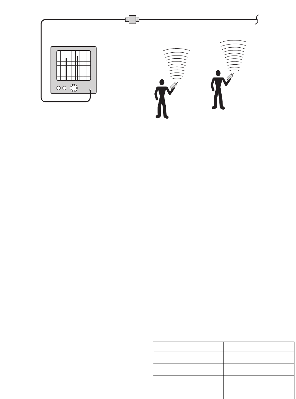
Procedure for Measuring Input Signal Levels
1) Set a spectrum analyzer for the center fre-
quency of one of the branches (look at the
specification drawing for this information).
2) Set the analyzer sweep width so that the entire
passband frequency range can be observed.
EXAMPLE
Gain Reduction (dB) = Minimum Isolation (dB) -
Measured Isolation (dB)
If the measured isolation is -75dB and the mini-
mum isolation is -80dB then the amount of gain
reduction required is: -80dB - (-75) = -5 dB
TXRX Systems Inc. Manual 7-9408-1.2 07/25/05 Page 13
61-38-05 UserMan page 13 of 38
3) The analyzer input attenuator should be set to
observe input signal levels from approximately -
80 dBm to 0 dBm.
4) Connect the analyzer to the section of the sig-
nal distribution system that is going to serve as
the input for the branch you want to observe
(see Figure 5).
5) Record the power level (in dBm) of all carriers in
the passband frequency range that are signifi-
cantly greater than the noise floor displayed on
the analyzer.
6) Repeat steps 1 through 5 for the remaining sig-
nal booster channels.
7) To find the total power being applied to the
channel, the calculations listed below must be
performed. The conversion chart at the rear of
the manual can be used. Here are the steps:
a) Convert all values in dBm to Watts
b) Total the power for all carriers in Watts
c) Convert the total power in Watts to dBm
Repeat the calculation for all of the branches in the
system. For example: suppose we have a signal
booster with a maximum gain of 70 dB. After
checking the input signal levels, it was determined
that there are three signals that are significantly
greater than the noise floor displayed on the ana-
lyzer. These signals have strengths of -45 dBm, -
43 dBm and -41 dBm.
First we use the conversion chart at the end of this
manual to convert the power levels in dBm to watts
so that we can add them together. The power in
watts is written in scientific notation but the chart
uses computer notation. For example, in the chart,
an exponent may be written as E-08. In conven-
tional mathematical notation E-08 is written 10-8.
The total power must be written as a number
between 0 and 10 to use the chart. Look up
1.611E-7 in the Watts column. This number falls
between -38 and -37 dBm so we chose -37
because it is the next higher value.
Power (dBm) Power (watts)
-45 dBm 3.16 x 10⁻⁸
-43 dBm 5.01 x 10⁻⁸
-41 dBm 7.94 x 10⁻⁸
TOTAL 16.11 x 10⁻⁸
S p e c t r u m A n a l y z e r
R a d i o 1
R a d i o 2
S I G N A L D I S T R I B U T I O N S Y S T E M
Figure 5: Typical test equipment setup for measuring input signal levels.
61-38-05 UserMan page 14 of 38
TXRX Systems Inc. Manual 7-9408-1.2 07/25/05 Page 14
Reduction of Incoming Signal Strength
Reducing the strength of offending signals may
require some or all of the following steps:
a) The addition of extra filtering. Consult TX RX
System's sales engineers for help in this
respect.
b) Modification of the signal distribution layout by
changing the type or location of pickup anten-
nas. This has to be approached in an empirical
way, that is, change-and-try until you get the
desired results. Sometimes changing from omni
to directional antennas will correct the problem.
Setting Signal Booster Gain
The Pre-Installation checks as outlined earlier
should have been performed to determine if gain
reduction will be necessary for your installation.
This can be due to low antenna isolation or exces-
sive input signal levels, or both. The actual amount
of gain reduction is determined by the largest num-
ber required because of either low isolation or
excessive signal levels.
For example, if the results of the isolation measure-
ment indicated the need for a gain reduction of -10
dB but signal level measurements indicate a need
for only a -5 dB gain reduction; then 10 dB is the
number required since both conditions are satis-
fied.
Gain Reduction Methods
As shipped from the factory, the system was setup
for maximum gain. Gain reduction is accomplished
by adding fixed attenuator pads or where even
greater reductions are required by bypassing one
section in a multi-section amplifier stage. Bypass-
ing of amplifier sections is preferred for large gain
reductions so that excessive noise levels are not
produced. Use of attenuator pads alone will reduce
gain but the signal booster will also amplify the
noise generated in the lower level sections.
The addition of attenuator pads may be necessary
in order to achieve the proper signal levels in the
overall communications system. This is quite com-
mon as actual signal losses in a radiating cable
system can vary somewhat from predicted theoret-
ical values. Fine adjustment of gain in communica-
tions systems with cascaded signal boosters can
be very important to keep performance uniform
over the entire length of the system.
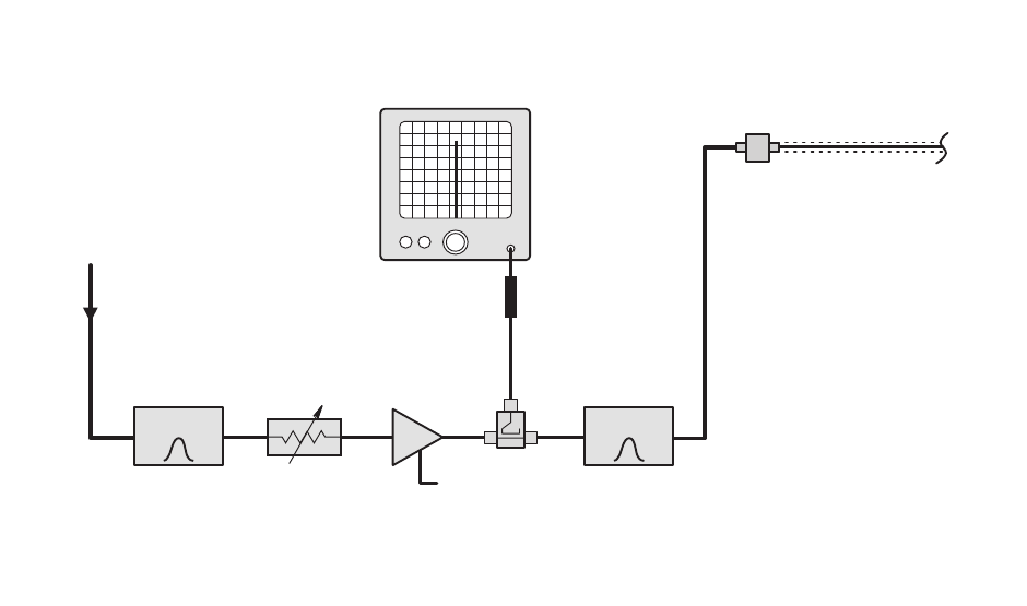
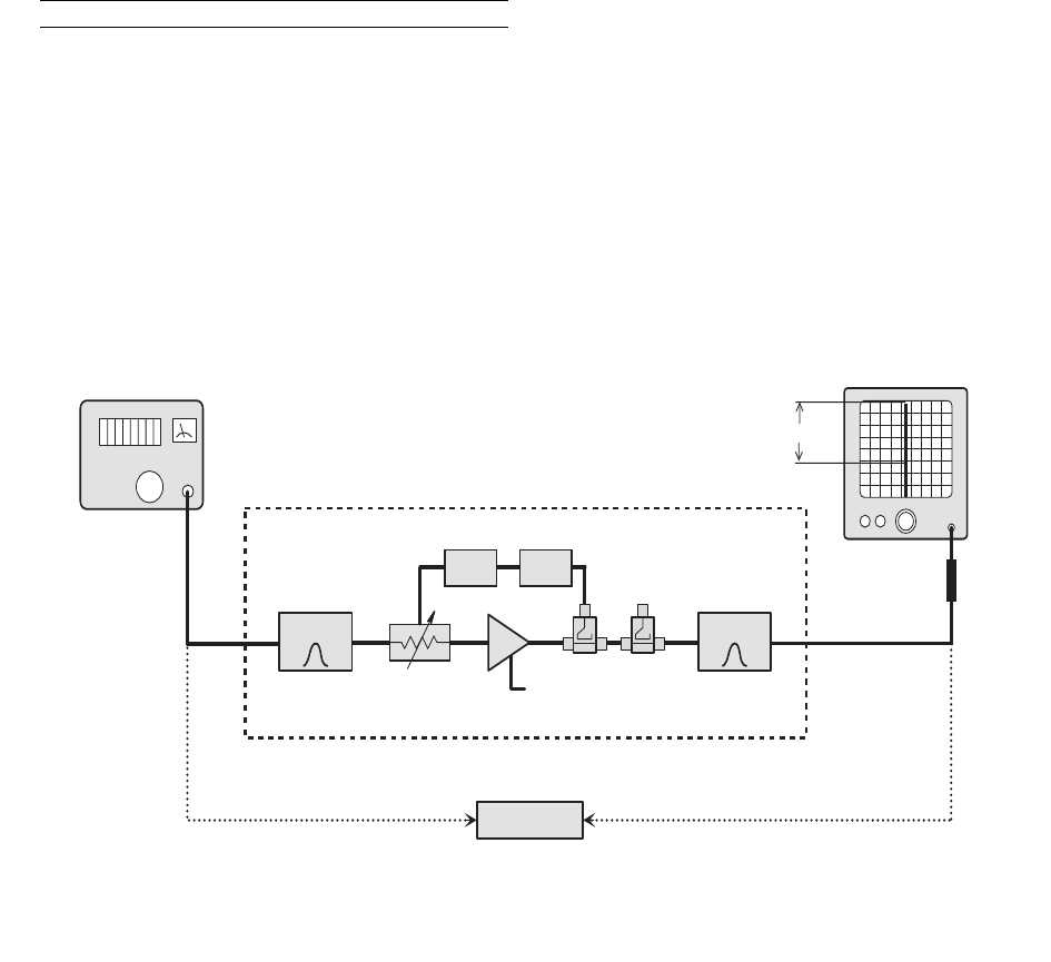
Figure 6 shows the use of a spectrum analyzer to
monitor signal levels in a signal booster. The ana-
lyzer connects to the signal sampler on the output
end of the branch to be tested. Attenuation is then
adjusted for the proper signal levels factoring in the
RF from Antenna or
Previous Repeater Amplifier
Signal Distribution System
FilterFilter
DC
Sampler
Variable
Attenuator
Spectrum
Analyzer
10 dB Pad
Amp
Figure 6: Observing RF power output of a signal booster using a spectrum analyzer.
TXRX Systems Inc. Manual 7-9408-1.2 07/25/05 Page 15
61-38-05 UserMan page 15 of 38
-50 dB coupling loss of the signal sampler and any
additional loss produced by attenuator pads on the
analyzer input. A pad on the analyzer input can
help to minimize measurement errors due to
VSWR mismatch that occurs with some analyzers.
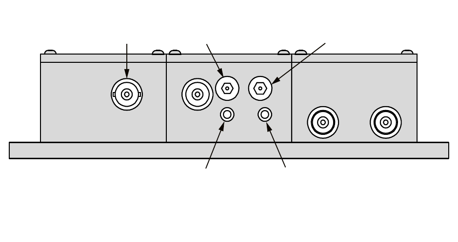
A pair of fixed attenuator pads (3 and 6 dB) are
supplied for the purpose of gain reduction. They
are mounted in clips to the top of the filter assem-
blies in the center of the unit. The pads’ attenuation
values are clearly labeled on the body of the atten-
uator. The correct position for adding fixed pads to
the system is at the input or output of the electronic
attenuator ports on the OLC assembly (shown as
the dotted outline symbols on the specification
drawing).
CAUTION: Any fixed attenuator pads
that are already connected into the
booster circuitry have been installed
at the factory and should not be
removed for any reason. Their func-
tion may be other than gain reduc-
tion.
BYPASSING AMPLIFIER SECTIONS
Sometimes the amount of gain reduction needed is
greater than the amount available with the fixed
attenuator pads alone. In this case, the first stage
of the three stage portion of amplifier assembly (3-
11423) in the uplink or downlink branch may be
bypassed. The individual stages of these multi-
stage amplifiers are connected together with short
lengths of coaxial cable. To bypass the first stage of
the driver amp remove the coax cable that inter-
connects the first and second stages of the driver
amplifier (see Figure 7). Move the input cable from
the input connector on the first stage to the corre-
sponding connector on the second stage of the
driver amp. The BNC RF input connector for each
amplifier stage is located furthest from the DC
input TNC connector. Keep in mind that the total
gain reduction is the sum of the added padding
plus the loss of gain for the bypassed amplifier sec-
tion. Quality 50 ohm terminations should be
installed on the open terminals of any bypassed
stage.
OPERATION
It is imperative that the pre-installation checks be
performed as outlined earlier. Failure to do so may
lead to unsatisfactory operation or damage to the
signal booster. All that is required in order to put
the system into operation after the installation is to
turn on the power supply assembly. The green LED
on the power supply will illuminate indicating nor-
mal operation. If the red LED on the power supply
assembly illuminates it indicates operation from the
backup power source.
SIGNAL FLOW
Signal flow through the system is illustrated using
the system block diagram that is shown in specifi-
cations drawing shipped with your system. The 61-
38-05 model signal boosters are composed of 2
branches, uplink and downlink. Because the uplink
Pre-Amp
(Single Stage)
Driver Amp
(3 Cascaded Stages)
RF
Output
RF
Input
RF
Output
RF
Input
Figure 7: 1stg/3stg amplifier assembly 3-11423.
61-38-05 UserMan page 16 of 38
TXRX Systems Inc. Manual 7-9408-1.2 07/25/05 Page 16
and downlink branches are physically identical,
both being constructed from the same set of sub-
assemblies, the signal flow discussion that follows
is applicable equally well to both branches. The
only difference between the two branches is the
tuning of their passbands.
Signals enter the system through the RF connec-
tors at the top of the cabinet. This is where the cus-
tomers antenna system is interfaced to the booster.
Input signals are immediately passed through pas-
sive filtering. The filter configurations can vary
slightly depending on the exact model of booster.
The filters provide the necessary isolation to allow
a pair of amplifier chains to be tied together provid-
ing bi-directional amplification with a single com-
mon input and common output connection. A
secondary but very beneficial effect of filtering is
instantaneous input and output frequency spec-
trum limiting which helps to prevent amplification of
unwanted channels. After filtering signals are then
applied to a preamplifier stage (the first section of
the multi-stage amplifier assembly 3-11423).
Following the preamplifier signals are applied to
the input of OLC (output level control) assembly 3-
6280. This assembly will attenuate the incoming
signals if necessary, to protect the final amplifier
from being overdriven by stronger than usual input
signals. The amount of attenuation is determined
by a reference voltage produced by a detector cir-
cuit built into the OLC assembly, which continu-
ously samples the output level of the final amplifier.
Once past the OLC assembly the signals are
applied to a driver amplifier composed of the final
three sections of the multi-stage amplifier assem-
bly 3-11423. The driver amplifier ensures that sig-
nals applied to the next stage, the final amplifier,
are at their optimum level and as free of any inter-
modulation distortions as possible. The high power
amplifier 3-11792 is a linear amp operated at con-
siderably less than it’s maximum output power to
insure maximum linearity.
Signals output from the high power amplifier stage
are routed to the detector input of the OLC assem-
bly by the first signal sampler 3-6999. The purpose
of the detected signal is to adjust the amount of
attenuation provided by the OLC assembly to the
incoming signal after the preamplifier stage. The
output of the high power amplifier is passed
through a second signal sampler 3-5969 that pro-
vides a -50 dB sampled signal as a convenience for
service technicians. The signals then pass through
passive filtering before leaving the signal booster at
the output connector located on the top of the cabi-
net. This is where the customers antenna system is
interfaced to the booster.
SYSTEM COMPONENTS
Each of the major system components used in the
model 61-38-05 family of signal boosters are briefly
discussed in the following text. Refer to the system
specification drawing that shipped with your system
during this discussion. The specification drawing
will include complete electrical and mechanical
specifications for your model. These include fre-
quency band, bandwidth, power gain and maxi-
mum power ratings. Recommended maximum
power ratings are shown for single signal and multi-
ple signal applications.
The functional block diagram included on the spec-
ification drawing shows all of the major subassem-
blies and their interconnections. Part numbers for
the major assemblies are also shown. We suggest
you look this drawing over carefully to fully familiar-
ize yourself with the unit.
Passive Filtering
The passive filters on the input and output ends of
each active section have one major purpose: they
provide the necessary isolation to allow a pair of
amplifier chains to be tied together providing bi-
directional amplification with a single common
input and common output connection. The filters
provide duplex operation and each one is tuned to
pass either the downlink or uplink frequency band.
They must provide a minimum isolation factor that
exceeds the amplifier gain by 15 dB in order to pre-
vent regenerative feedback and maintain spurious-
free operation. In the VHF spectrum, these filters
are usually constructed from cascaded coaxial
bandpass cavities or multistage helical bandpass
filters. Bandpass filters may be augmented by
notch filters using the same basic resonator style
(coaxial or helical). Notching filters allow the filter
response to be closely tailored to the specific isola-
tion requirements for the specific uplink and down-
link frequency band separation. Typical VHF
frequency pairs (repeater input/output frequencies
= Down/uplink frequencies) vary considerably in
frequency separation making flexibility in tailoring
the filter response a necessity for proper operation.
When necessary, single channel bandpass filters
may also be used as an augment to facilitate close-
spaced frequency operation without interference.

TXRX Systems Inc. Manual 7-9408-1.2 07/25/05 Page 17
61-38-05 UserMan page 17 of 38
Single channel bandpass filters are generally 4-
pole crystal filters using piezo-electric resonators.
A secondary but very beneficial effect of filtering is
instantaneous input and output frequency spec-
trum limiting which helps to prevent amplification of
unwanted channels.
While filtering can reduce or eliminate spurious
output signal, this is a tertiary function in the VHF
signal booster because this booster family uses
Class-A linear amplifiers that generate much lower
harmonic content than the typical Class C or D
amplifier used in typical landmobile transmitters.
The input and output filter assemblies used in the
model 61-38-05 signal booster systems are com-
posed of helical preselectors, 2” square bandpass
cavities, and 2” square notch cavities. These filters
all have a carefully shaped response curves that
define the pass windows for the booster.
The helical preselectors are composed of four cas-
caded helical cavities. The cavities are intercon-
nected with critical length cables to synthesize a
shaped response. The bandpass filters pass one
narrow band of frequencies (the passband) and
attenuate all others with increasing attenuation
above and below the pass frequencies. The inser-
tion loss setting determines the filters selectivity
and maximum power handling capability. Insertion
loss is set at the factory. The notch filters are used
to notch out a very narrow range of frequencies
and improve the skirt selectivity of associated
bandpass filters.
The filters used in the booster are factory pretuned
and do not require any adjustment. The filters are
easy to misalign. Being passive devices using sil-
ver plated contacts means they requires no mainte-
nance and will stay tuned indefinitely unless they
are physically damaged or tampered with. If it is
suspected that a filter is out of alignment, we sug-
gest returning it to the factory for re-alignment.
However, if the necessary test equipment is avail-
able then the tuning procedure outlined later in this
manual may be used to put it back on frequency.
DC Regulator (3-5969)
The DC regulator receives 24.7 VDC from the
power supply assembly through it's input 'TNC'
connector. Two regulator assemblies are used, one
for each signal branch in the bi-directional system.
each of the regulators provides two different output
voltages, +15 VDC and +21.7 VDC. A minimal volt-
age differential of 3 volts is required between the
input and the output of the 3-5969 regulator in
order to maintain proper operation. The regulator
assembly can provide up to 5 amps of total current.
The regulator circuit uses two conventional IC reg-
ulator chips. An LM338K is used to produce the
fixed 15 VDC, and an LM340K is used for the vari-
able output which is factory adjusted to +21.7 VDC.
Test jacks (red & black) are available on the regula-
tor chassis for measuring the input, fixed-output,
and the variable-output voltages. The regulator has
an access hole on the side of it's case for adjusting
the variable-output voltage. A thin blade screw-
driver is used to engage a trim-pot type variable
resistor R2 which is then rotated until the desired
output voltage is obtained. Adjustment of the regu-
lator is only required after making repairs to the
regulator circuitry.
OLC Assembly (3-6280)
The OLC assembly 3-6280 is used in both
branches of the system is divided into three
shielded compartments; one housing the RF to DC
converter, the second a DC control circuit, and the
third containing the PIN diode attenuator circuit. A
test point is provided for measuring the voltage that
is applied to the PIN diode attenuator. A second
test point allows measurement of the voltage sup-
plied by the converter to the DC control circuit (see
Figure 8). Regulated 21.7 VDC is supplied to the
"TNC" female connector to power the assembly.
The RF to DC converter receives RF from the sig-
nal sampler and produces a negative polarity DC
output voltage that is proportional to the RF signal.
A Schottky Barrier diode is used as the detector.
Because this detector circuit has a very high input
impedance, the magnitude of the voltage that it
produces will vary if the length of the coaxial cable
which connects it to the signal sampler changes.
Therefore, it is important not to change this length.
The voltage produced by the RF to DC converter is
directly proportional to the output signal strength of
the final amplifier. The voltage is supplied to the DC
control circuit at the non-inverting terminal of op-
amp IC2. A variable reference voltage is applied to
the inverting terminal of the same op-amp. Variable
resistor VR2 is used to set the magnitude of this
reference voltage and controls the level at which
gain reduction will start to occur. As the signal
strength increases the output voltage of the con-
verter, which is of negative polarity, becomes
61-38-05 UserMan page 18 of 38
TXRX Systems Inc. Manual 7-9408-1.2 07/25/05 Page 18
larger. This change causes the output of IC2 to
also become increasingly negative. This output
voltage is connected via diode D1 to bias the PIN
diode attenuator. As this voltage becomes more
negative, the attenuation is increased thus achiev-
ing a certain range of gain control. Diode D1
insures that the gain control voltage is always posi-
tive and never goes below 0 volts. In actual opera-
tion, OLC operation is set to commence when the
power output of the final amplifier reaches its maxi-
mum two-carrier level as shown on the specifica-
tion drawing.
Two other IC’s are mounted on the DC control cir-
cuit board. IC1 is a 10 volt regulator that supplies
DC to the other two chips. Variable resistor VR1 is
used to set this voltage. IC3 is a voltage inverter
that produces -4.5 volts which is applied to the op-
amp IC2. This negative bias allows the output volt-
age of IC2 to closely approach 0 volts.
The PIN diode attenuator board has two diodes
that are used in series to extend the attenuation
range. The diodes are always forward biased with
minimum forward resistance and insertion loss
occurring at about 20 ma of current.
Pre-Amplifier Stage (3-11423)
The pre-amplifier consists of the 400 milliwatt
amplifier stage connected to the input of the OLC
assembly. The preamp is the first stage of the four
identical stages found in the amplifier assembly 3-
11423. This amplifier stage is used to insure that a
sufficient signal level is applied to the OLC assem-
bly.
The 1-section/3-section amplifier assembly (3-
11423) is composed of four individual and identical
amplifier sections. Each of the individual sections
(part# 3-8089) are complete 400 milliwatt amplifi-
ers. The individual sections are mounted on a com-
mon mounting panel and have a common DC
distribution bus running internally between them.
Each section provides 18.5 dB of gain with a power
requirement of 21.7 VDC (nominal) and a typical
current draw of 121 ma. The maximum single car-
rier power output is 400 milliwatts.
Each 400 milliwatt amplifier section consists of two
circuits, the amplifier circuit (3-8087) and the bias
regulator circuit (3-10742). Both of these circuits
are housed in their own enclosures which are then
physically joined together to make up one section.
The circuits are electrically joined using feed-thru
capacitors Cf1 and Cf2.
The amplifier circuit uses a linear RF transistor Q1
(Phillips part# BFQ34/01) which is operated in a
class "A" configuration in order to keep any inter-
modulation distortion to a minimum. The RF tran-
sistor is biased for a nominal collector current of
121 ma. A bias regulator circuit is used to keep the
collector current constant with changes in tempera-
ture. Narrow band matching techniques are used in
this amplifier and it will require tuning if the transis-
tor or matching network components are replaced.
CONTROL
VOLTAGE
+15 VDC
OUTPUT INPUT
OLC Voltage
Adjust
10V Regulator
Adjust
RF from
Sampler
Detector
Voltage
Test Point
OLC
Voltage
Test Point
RF to DC
Converter
Pin Diode
Attenuator
Figure 8: OLC assembly 3-6280.
TXRX Systems Inc. Manual 7-9408-1.2 07/25/05 Page 19
61-38-05 UserMan page 19 of 38
The bias regulator circuit uses an Op-Amp compar-
ator IC1 to supply a variable bias current which var-
ies as required to keep the RF transistors collector
current constant. Current to the collector of the RF
transistor flows through resistor R1. The voltage at
the collector side of this resistor is applied to the
non-inverting input of IC1. Voltage divider R2 / R4
sets the desired reference voltage on the inverting
terminal of IC1. The variable output voltage at pin 6
of IC1 is then applied to the base of the RF transis-
tor. The bias on the RF transistor will now vary in
such a way as to keep the voltage at the collector
end of R1 equal to the reference voltage provided
by divider R2/R4, thus keeping the RF transistor's
collector current constant (121 ma nominal).
Repair or replacement of bias circuit components
does not necessitate retuning of the amplifier.
Driver Amplifier Stage (3-11423)
The remaining three stages of the amplifier assem-
bly 3-11423 are used to form a driver amplifier
which amplifies the passband signals to levels suf-
ficient for driving the input of the final High Power
Amplifier stage. Each of the three individual 400
milliwatt stages in the driver amp are identical and
were discussed in detail in the earlier sub-section
entitled "Pre-Amplifier (3-11423)".
High Power Amplifier Assembly (3-11792)
This amplifier stage uses a single ultra-linear RF
transistor. The 3.0 watt rating indicates the maxi-
mum safe output from this amplifier assembly
using a single carrier. The actual maximum allow-
able power output with multiple carriers is much
lower and is determined by the maximum allowable
intermodulation product level. It is also limited by
the collector to emitter breakdown rating of the RF
transistor.
This amplifier stage is physically mounted to the
inside of the heatsink located on the side of the
cabinet. The amplifier draws a nominal 420 ma. A
bias regulator circuit within the amplifier assembly
is used to keep the collector current of the RF tran-
sistor constant with changes in temperature. This
amplifier has a minimum gain of 18 dB, 19 dB typi-
cal. The amplifier uses narrow band matching tech-
niques and will require tuning if the transistor or
matching network components are replaced.
Signal Sampler (3-6999)
Following the output of the power amplifier assem-
bly is a -25 dB signal sampler. This sampler is used
to couple the output signal level back to the OLC
assembly.
Signal Sampler (3-3569)
This sampler is located at the output of the uplink
and downlink branches and is used for connecting
test equipment to the branch, such as a spectrum
analyzer. The 3-3569 signal sampler capacitively
couples signals to the sample port at a -50 dB
level.
DC Junction Box (3-6254)
This assembly has no internal components and is
used to couple battery backup voltage (supplied by
the customer) to the power supply.
Power Supply Assembly (3-15503)
The power supply assembly consists of two sub-
assemblies, an OEM power supply module and a
failure switching circuit. The switching circuit is
designed to pass the output from either the OEM
power supply or the backup batteries to the TNC
style output connectors which are labeled “24.7
VDC Output” located on the assemblies front panel
next to the fuses.
The output of the OEM supply (part# 8-15495) is
applied to the output TNC connectors through relay
K2 pins 9 and 10. The voltage feed is protected by
fuse F1 (10 amp). During normal operation relay
K2 is energized connecting pin 9 to pin 10. If AC
power is interrupted relay K2 becomes de-ener-
gized connecting pin 9 to pin 8 which is fed from
the battery backup. This will pass battery voltage to
the output TNC connectors.
With AC voltage applied to relay K2 pin 6 will be
connected to pin 7 completing the ground path for
the green LED D2. When K2 is de energized indi-
cating AC power failure pin 5 is connected to pin 6
completing the ground path for the red LED D1
indicating the unit is operating on DC backup volt-
age.
The Loss of AC Alarm Terminal block is provided
for customer convenience. Under normal system
operation, when the OEM supply voltage is active,
the NC terminal is shorted to the COM terminal
because pins 5 and 6 are connected by relay K1.
K1 is energized whenever the AC power supply is
active. When the system is running on battery
backup voltage the NO terminal is connected to the
COM terminal because pin 5 will now be con-
61-38-05 UserMan page 20 of 38
TXRX Systems Inc. Manual 7-9408-1.2 07/25/05 Page 20
nected to pin 4. Relay K1 is de-energized when the
AC power supply is off.
PERFORMANCE SURVEY
It is a good idea to document the performance of
the system after installation so that a reference
exists for future comparisons. This information can
make troubleshooting an interference problem or
investigation of a complaint about system perfor-
mance much easier. If there are coverage prob-
lems with a system, this survey will usually reveal
them allowing corrective measures to be taken
before the system is put into routine use. The fol-
lowing is an outline of how to do such a survey.
Because the nature of each installation can be
quite different, only a broad outline is given.
1) Measure the gain of the signal booster being
careful not to exceed the maximum input level.
Figure 9 shows this being done using a signal
generator and spectrum analyzer. This is basi-
cally a substitution measurement. Record the
measured values for each passband.
2) Each branch of the signal booster system is
equipped with a -50 dB signal sampler port fol-
lowing the final output amp (part of the OLC
assembly). This port is for the connection of test
equipment such as a spectrum analyzer and
will allow the observation of the amplifier output
at a considerably reduced output level. This
decoupling figure needs to be added to a mea-
sured signal value in order to arrive at the actual
signal level. OLC assemblies appear in sche-
matic representation on the specification draw-
ings.
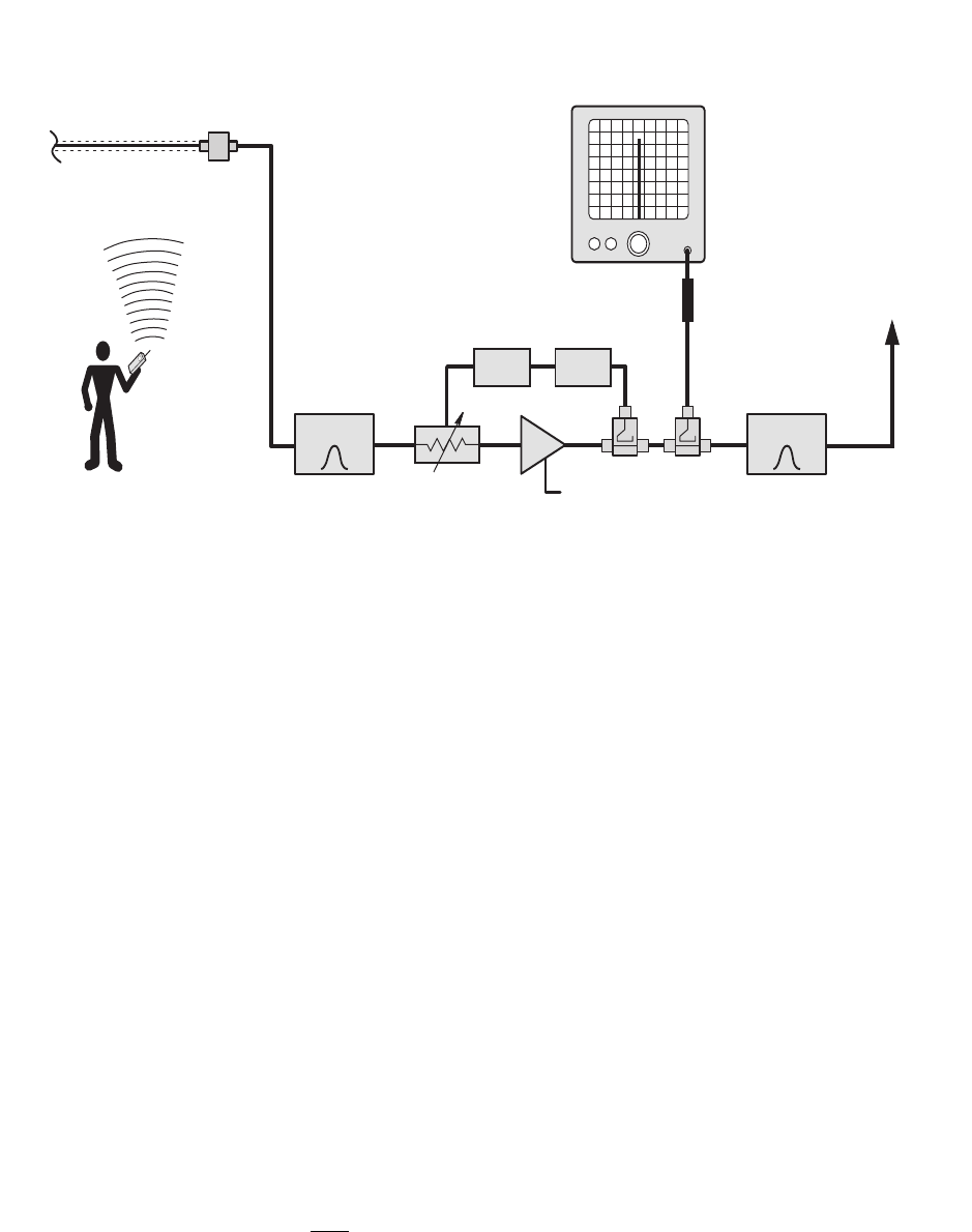
3) With a spectrum analyzer connected to the sig-
nal sampler port for the branch under test (see
Figure 10), have personnel with handheld
radios move to predetermined points and key
their radios. Record the level of these signals as
observed on the analyzer and also record the
location of the person transmitting. In this way, a
map of the systems performance can be gener-
ated.
4) For branches that amplify signals coming from a
fixed antenna or station, record the level of all
the desired incoming signals for future refer-
ence.
FIELD ADJUSTMENTS
The following information is provided in support of
field support activities, including routine mainte-
nance, repairs, adjustments and tuning. It is
DC
Sampler Sampler
Detector
Electronic
Attenuator
OLC Assembly
Filter Filter
Amp
DC
Control
ZERO
REFERENCE
GAIN
10 dB Pad
SIGNAL
GENERATOR
SPECTRUM
ANALYZER
Figure 9: Test equipment interconnection for measuring signal booster gain.
TXRX Systems Inc. Manual 7-9408-1.2 07/25/05 Page 21
61-38-05 UserMan page 21 of 38
assumed that the procedures will be carried out by
a qualified electronics technician observing all
standard safety practices.
Filter Tuning
Filters used in TX RX Systems’ signal boosters are
passive devices of rugged electrical and mechani-
cal design. They are tuned at the factory for the
original design requirements and require no adjust-
ment or maintenance. These devices will stay prop-
erly tuned unless they have been physically
damaged or are tampered with. Filter tuning falls
into two categories; retuning to the original fre-
quency such as when a filter is being repaired or
replaced, or tuning to new frequencies.
A number of points need to be considered before
attempting to tune a signal booster to frequencies
different from the original.
1) The Frequency Range Specification for the 61-
38-05 signal booster family does not mean that
an individual signal booster is field tunable over
the entire indicated frequency range. This spec-
ification only indicates the frequency range for
which the 61-38-05 components are intended.
Many of the filter assemblies used in a particu-
lar booster maintain reasonable performance
over a range that is within ± 2% of the original
frequency. For greater changes in frequency,
the performance of the filters may degrade
severely. Therefore some filters may need to be
replaced or modified when large frequency
changes are made.
2) In a bidirectional system, will the new inbound
and outbound channels have the same fre-
quency separation from each other as the origi-
nal ones? Frequency separation in bidirectional
designs is one of the prime design criteria. If the
frequency separation decreases from the origi-
nal, the filters will provide less isolation so the
gain may also have to be reduced to prevent the
signal booster from oscillating. Increases in fre-
quency separation are more easily accommo-
dated.
3) If the bandwidth requirement increases, the
bandpass filters may not pass all of the new fre-
quencies. In most cases, the bandwidth of the
bandpass filters cannot be changed by the cus-
tomer.
DC
Sampler Sampler
Detector
Electronic
Attenuator
OLC Assembly
Filter Filter
Amp
DC
Control
10 dB Pad
SPECTRUM
ANALYZER
SIGNAL DISTRIBUTION SYSTEM
BOOSTED
RF SIGNAL
Figure 10: Test equipment interconnection for surveying performance.
61-38-05 UserMan page 22 of 38
TXRX Systems Inc. Manual 7-9408-1.2 07/25/05 Page 22
4) The amplifier assemblies may have to be
retuned.
5) The length sensitive interconnect cables may
need to be changed.
If you are not sure about tuning the signal booster
system to new frequencies then contact your TX
RX Systems, Inc. representative. Our knowledge-
able engineering and sales staff are happy to dis-
cuss what it will take to tune your system to the
new frequencies.
Helical Preselectors
The helical preselectors are composed of four cas-
caded individual helical cavities. The cavities are
interconnected with critical length cables to synthe-
size a shaped response. This filter assembly can
not be tuned by tuning the individual cavities, the
assembly must be tuned as a whole. The band-
width of the filter is determined by the critical align-
ment of internal “reactive” components. Bandwidth
is therefore fixed by construction in this type of filter
The helical preselectors are pretuned at the factory
for a specific bandwidth and no attempt should be
made to adjust the bandwidth.
REQUIRED EQUIPMENT
A two channel network analyzer that simulta-
neously displays both transmission and reflection
is best for properly tuning a preselector. A single
channel tracking generator / spectrum analyzer
combination may be adequate but insure that it is
accurate enough to verify factory specifications. A
return loss bridge would also be required when
using a tracking generator / spectrum analyzer.
Skill and experience are also needed and the per-
sonnel doing the work should be thoroughly famil-
iar with the test equipment.
TUNING PROCEDURE
The following is an outline of the general proce-
dure.
1) Connect test equipment as shown in Figure 11.
2) Set the analyzer to the desired center fre-
quency and desired bandwidth.
3) Loosen the tuning rod locking nuts.
4) If the preselector is severely out of tune, set the
analyzer for 10 dB/div vertical scale and alter-
nately adjust the tuning rods in pairs working
from the center to the end rods for maximum
signal at the center frequency. Start with the
center rods and then move to the outer rods.
5) Repeat step 4 tuning to maximize the signal at
the center frequency. The response should start
to take on the desired shape and symmetry.
Setup the analyzer for 2 dB/div and then re-
adjust the rods in the same fashion. Make sure
that the response is relatively symmetrical. Fine
adjust the tuning rods as necessary to adjust
symmetry.
6) When using the spectrum analyzer/tracking
generator, the equipment must be connected as
shown in Figure 12 in order to check the return
loss curve. The network analyzer will show the
return loss curve as a matter of course.
7) Lock all tuning rods after the desired response
is obtained. Note that a slight dissymmetry in
Analyzer
Input
Generate
Output
+30
+40
+20
+10
0
-10
-20
-30
-40
4 Section
Helical Preselector
Figure 11: Preselector tuning.
TXRX Systems Inc. Manual 7-9408-1.2 07/25/05 Page 23
61-38-05 UserMan page 23 of 38
either the transmission or reflection response
may be unavoidable.
Bandpass Filters
The bandpass filters pass one narrow band of fre-
quencies (the passband) and attenuate all others
with increasing attenuation above and below the
pass frequencies. The insertion loss setting deter-
mines the filters selectivity and maximum power
handling capability. Insertion loss is set at the fac-
tory.
Cavity tuning follows a two step process. First the
cavity is temporarily disconnected from the system
and rough tuned, this will ensure the response
curve is very close to it's ideal. Next the cavity is
reconnected to the system and fine tuned. This is
done in large systems such as the model 61-38-05
in order to eliminate any slight distortions which
could result from interactions with other cavities.
The pass frequency is the only field adjustable
parameter found in the individual Bandpass reso-
nant cavity filters. Adjustment of the tuning rod on
these filters will allow the passband to be centered
at the desired frequency. The insertion loss of each
cavity is not field adjustable.
REQUIRED EQUIPMENT
Due to the sensitivity of the adjustments, it is
strongly recommended that the proper equipment
be used when tuning the individual filters, other-
wise the filter should be sent to the factory or an
authorized representative for retuning. The follow-
ing equipment or it's equivalent is recommended in
order to properly perform the tuning adjustments.
1. IFR A-7550 spectrum analyzer with optional
tracking generator installed.
2. 7/16” wrench.
3. Double shielded coaxial cable test leads
(RG142 B/U or RG223/U).
4. Female union (UG29-N or UG914-BNC).
TUNING PROCEDURE
The following is an outline of the general proce-
dure.
1. Turn off the system power and disconnect the
cables that are attached to the cavity.
2. Setup the analyzer / generator for the desired
frequency and bandwidth (center of display)
and also a vertical scale of 2 dB/div. Set the
sweep width of the display to 100 KHz.
4. A zero reference must first be established at the
IFR A-7550 before making measurements. This
is accomplished by temporarily placing a
"female union" between the generator output
and the analyzer input.
5. The flat line across the screen is the generator's
output with no attenuation, this value will
become our reference value by selecting the
4 Section
Helical Preselector
Analyzer
Input
Generate
Output
+30
+40
+20
+10
0
-10
-20
-30
-40
Bridge
50 ohm Load
Figure 12: Observing preselector return loss.
61-38-05 UserMan page 24 of 38
TXRX Systems Inc. Manual 7-9408-1.2 07/25/05 Page 24
"MODE" main menu item and choosing the
"STORE" command. This will store the flat-line
value in the analyzer's internal memory.
6. Next select the "DISPLAY" main menu item and
choose the "REFERENCE" command. This will
cause the stored value to be displayed on the
screen as the 0 dB reference value.
7. The resonant frequency of the filter is checked
by connecting the tracking generator to the
input of the cavity filter assembly while the
spectrum analyzer is connected to the output,
as shown in Figure 13.
8. Insure the IFR A-7550 menu's are set as fol-
lows:
DISPLAY - line
MODE - live
FILTER - none
SETUP - 50 ohm/dBm/gen1.
9. Adjust the pass frequency by setting the peak
(minimum loss value) of the response curve to
the desired frequency (should be the center-
vertical graticule line on the IFR A-7550's dis-
play). The resonant frequency is adjusted by
adjusting the tuning rod, which is a sliding
adjustment (invar rod) that rapidly tunes the fil-
ter's response curve.
Pseudo-Bandpass Filters
The pseudo-bandpass filter passes a relatively nar-
row band of frequencies and rejects (notches out)
a relatively wide frequency band. These cavity fil-
ters are two inch square, helical type resonators
that include a tunable notching section, refer to
Figure 14. These filters are pretuned and require
no adjustment unless they have been damaged
and repaired or tampered with in some way. They
are passive devices that require no maintenance.
Female Union
Used to determine 0 dB reference
Analyzer
Input
Generate
Output
+60
+80
+40
+20
0
-20
-40
-60
-80
Tracking Generator
2" Sq. Bandpass
Cavity Filter
Figure 13: Bandpass filter tuning.
Sliding Main
Tuning Rod
(Passband)
Main Tuning
Lock Nut
Rejection
Notch Tuning
Capacitor
Input/Output
Connectors
Figure 14: The Pseudo-bandpass filter.
TXRX Systems Inc. Manual 7-9408-1.2 07/25/05 Page 25
61-38-05 UserMan page 25 of 38
REQUIRED EQUIPMENT
Due to the sensitivity of the adjustments, it is
strongly recommended that the proper equipment
be used when tuning the individual filters, other-
wise the filter should be sent to the factory or an
authorized representative for retuning. The follow-
ing equipment or it's equivalent is recommended in
order to properly perform the tuning adjustments.
1) IFR A-7550 Spectrum Analyzer / Tracking Gen-
erator combination.
2) Eagle Model RLB150BN3 Return Loss Bridge
(35 dB directivity).
3) Double shielded coaxial cable test leads
(RG142 B\U or RG223/U).
4) 50 Ohm load with at least -35 dB return loss
(1.10:1 VSWR).
5) Insulated metal blade tuning tool for adjusting
ceramic and/or piston variable capacitors.
Similar equipment from other manufacturers
should yield acceptable results.
TUNING PROCEDURE
The following general procedure assumes familiar-
ity with the use of a tracking generator.
1) Set the tracking generator to a center frequency
of the filter to be tuned. Set the tracking genera-
tor for 0 dBm output and a 10 dB/div scale.
Connect the equipment as shown in Figure 15
but leave the load port of the bridge uncon-
nected.
2) Set a 0 dB return loss reference. For the IFR A-
7550 perform the following procedure:
a) Make sure that the unit is in "LIVE" mode
when performing step 7.
b) From the Mode Menu, "STORE" the above
trace.
c) Switch to the Display Menu and select
"REF". The trace should appear at the 0 dB
level.
3) Connect the load port of the bridge to the filter
as shown in figure 15.
4) Adjust the cavity main tuning rod for maximum
return loss at the center frequency.
5) Set the tracking generator for the center fre-
quency of the filter and connect the test leads
as shown in Figure 16 but first temporarily con-
nect the leads together through a female barrel
connector and set a zero dB loss reference. On
the IFR A-7550 proceed as follows:
a) Make sure that the unit is in "LIVE" mode when
performing step 2.
LOAD
REFLECTED
SOURCE
Analyzer
Input
Generate
Output
+30
+40
+20
+10
0
-10
-20
-30
-40
RLB - 150 Bridge
2" Square VHF
Pseudo-Bandpass Filter
Tracking Generator
Tune
Figure 15: Tuning the Pseudo-bandpass filter
for maximum return loss.
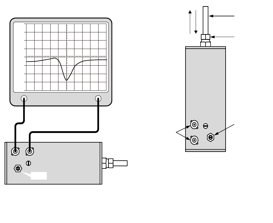
61-38-05 UserMan page 26 of 38
TXRX Systems Inc. Manual 7-9408-1.2 07/25/05 Page 26
b) From the Mode Menu, "STORE" the above
trace.
c) Switch to the Display Menu and select "REF".
6) Connect the leads to the cavity as shown in fig-
ure 16 and use a tuning tool or small screw
driver to engage the notch tuning capacitor and
rotate it to obtain maximum attenuation at the
notch frequency.
7) Tighten the cavity main tuning locking nuts.
The cavity may be put back into the repeater ampli-
fier.
Notch Filters
The notch filter passes a relatively wide band of
frequencies while rejecting (notches out) a very
narrow band of frequencies. They are used to
improve the skirt selectivity of associated band-
pass filters. These cavity filters are two inch
square, helical type resonators that include a tun-
able notching section, refer to Figure 17. These fil-
ters are pretuned and require no adjustment unless
they have been damaged and repaired or tam-
pered with in some way. They are passive devices
that require no maintenance.
REQUIRED EQUIPMENT
Due to the sensitivity of the adjustments, it is
strongly recommended that the proper equipment
be used when tuning the individual filters, other-
wise the filter should be sent to the factory or an
authorized representative for retuning. The follow-
ing equipment or it's equivalent is recommended in
order to properly perform the tuning adjustments.
1) IFR A-7550 Spectrum Analyzer / Tracking Gen-
erator combination.
2) Eagle Model RLB150BN3 Return Loss Bridge
(35 dB directivity).
3) Double shielded coaxial cable test leads
(RG142 B\U or RG223/U).
Analyzer
Input
Generate
Output
+30
+40
+20
+10
0
-10
-20
-30
-40
2" Square VHF
Pseudo-Bandpass Filter
Tracking Generator
Tune
Figure 16: Tuning the Pseudo-bandpass filter
for maximum attenuation.
Sliding Main
Tuning Rod
(Notch)
Main Tuning
Lock Nut
Passband
Tuning
Capacitor
Input/Output
Connectors
Figure 17: The Notch filter.
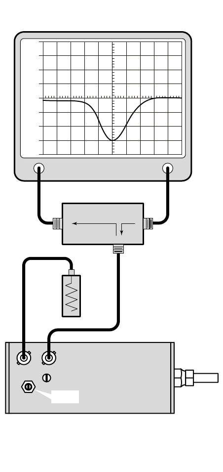
TXRX Systems Inc. Manual 7-9408-1.2 07/25/05 Page 27
61-38-05 UserMan page 27 of 38
4) 50 Ohm load with at least -35 dB return loss
(1.10:1 VSWR).
5) Insulated metal blade tuning tool for adjusting
ceramic and/or piston variable capacitors.
Similar equipment from other manufacturers
should yield acceptable results.
TUNING PROCEDURE
The following general procedure assumes familiar-
ity with the use of a tracking generator.
1) Set the tracking generator to a center frequency
of the filter to be tuned. Set the tracking genera-
tor for 0 dBm output and a 10 dB/div scale.
Connect the equipment as shown in Figure 18
but leave the load port of the bridge uncon-
nected.
2) Set a 0 dB return loss reference. For the IFR A-
7550 perform the following procedure:
a) Make sure that the unit is in "LIVE" mode
when performing step 7.
b) From the Mode Menu, "STORE" the above
trace.
c) Switch to the Display Menu and select
"REF". The trace should appear at the 0 dB
level.
3) Connect the load port of the bridge to the filter
as shown in figure 18.
4) Adjust the cavity main tuning rod for maximum
attenuation at the notch frequency.
5) Set the tracking generator for the center fre-
quency of the filter and connect the test leads
as shown in Figure 19 but first temporarily con-
nect the leads together through a female barrel
connector and set a zero dB loss reference. On
the IFR A-7550 proceed as follows:
a) Make sure that the unit is in "LIVE" mode when
performing step 2.
b) From the Mode Menu, "STORE" the above
trace.
c) Switch to the Display Menu and select "REF".
6) Connect the leads to the cavity as shown in fig-
ure 19 and use a tuning tool or small screw
driver to engage the notch tuning capacitor and
rotate it to obtain maximum return loss at the
center frequency.
7) Tighten the cavity main tuning locking nuts.
The cavity may be put back into the repeater ampli-
fier.
LOAD
REFLECTED
SOURCE
Analyzer
Input
Generate
Output
+30
+40
+20
+10
0
-10
-20
-30
-40
RLB - 150 Bridge
2" Square VHF
Notch Filter
Tracking Generator
Tune
Figure 18: Tuning the Notch filter for maximum
return loss.
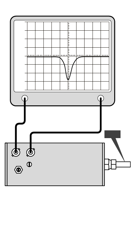
61-38-05 UserMan page 28 of 38
TXRX Systems Inc. Manual 7-9408-1.2 07/25/05 Page 28
Single Section Amplifier Subassemblies
Amplifiers with 400 Milliwatt RF power output rat-
ings are manufactured by TX RX Systems, Inc. for
use in the model 61-38-05 family of signal boost-
ers. These amplifiers utilize bi-polar transistors
operating as class-A linear amplifiers with varying
RF power output capability. They offer a good com-
promise between low noise figure and low levels of
intermodulation distortion. In addition, these ampli-
fiers use narrow band impedance matching cir-
cuitry which offers significant improvements in
noise figure compared to broadband designs. How-
ever, narrow band circuits necessitate having to
tune the matching networks to obtain best perfor-
mance. This tuning procedure needs to be done
when the RF transistor and/or matching network
components are replaced.
Each single amplifier section (see Figure 20) uses
a bias regulator circuit to keep the RF transistor
biased for constant collector current with changes
in temperature. The collector current remains con-
stant when these amplifiers are running properly.
The actual value of bias current will be different for
different types of amplifiers but can also vary
slightly if the power supply voltage varies. All ver-
sions of the current production bias regulators are
designed for fixed values of RF transistor collector
current.
The multi section amplifier assembly 3-11423 is a
combination of individual single section subassem-
blies (part # 3-8089) which have a 400 Milliwatt
output power rating per section. These single sec-
tion subassemblies are interconnected with short
lengths of double shielded coaxial cable for the RF
interconnection. The individual sections are
mounted on a common bracket with a DC distribu-
tion wire running internally between sections. A
multi section amplifier is tuned on a per section
basis. Never attempt to tune the interconnected
sections.
AMPLIFIER TUNING
Field repair and tuning of our amplifiers is sup-
ported by TX RX Systems Inc. and the following
procedure will allow satisfactory operation to be
obtained. At the factory, TX RX amplifiers are tuned
using two channel network analyzers that allow
adjustment of both gain, input/output return loss
and verification of reverse isolation. After this tun-
ing, the amplifiers are checked with an advanced
noise figure measurement system and are fine
tuned to obtain best noise figure. Because this
equipment is rarely available in even the most well
equipped service centers, we recommend return-
ing the amplifier to the factory for repair and retun-
ing if the specified noise figure has to be obtained.
In actual practice, most of the amplifiers retuned in
the field will exhibit noise figures that range from
being equal to the published specification or
exceed it by 0.5 to 2 dB. Low noise figure may be of
minimal importance in any system where very
weak signal sensitivity is not an issue.
REQUIRED EQUIPMENT
The following procedure was developed to be prac-
tical as a field bench service procedure. This pro-
cedure is intended for single sections only. All multi
section TX RX amplifiers are composed of cas-
caded single sections interconnected with short
lengths of double shielded coaxial cable. Individu-
ally tuned single sections do not require any further
adjustment when they are connected together
Analyzer
Input
Generate
Output
+30
+40
+20
+10
0
-10
-20
-30
-40
2" Square VHF
Notch Filter
Tracking Generator
Tune
Figure 19: Tuning the Notch filter for max attenuation.
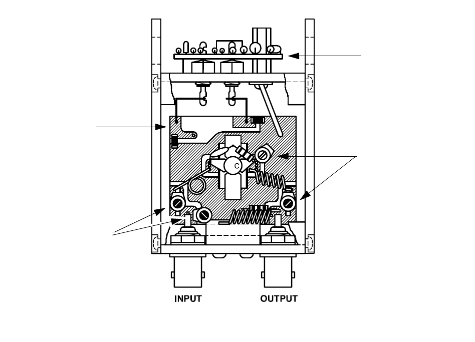
TXRX Systems Inc. Manual 7-9408-1.2 07/25/05 Page 29
61-38-05 UserMan page 29 of 38
forming a multi-section subassembly. This proce-
dure requires the following equipment:
1) IFR A-7550 Spectrum Analyzer / Tracking Gen-
erator combination.
2) Eagle RLB150N3 Return Loss Bridge or equiv-
alent (35 dB directivity).
3) Double shielded coaxial cable test leads
(RG142 B\U or RG223/U).
4) 50 Ohm load with at least -35 dB return loss
(1.10:1 VSWR). JFW Industries model 50T-007
or equivalent.
5) Regulated DC power supply at the required
voltage.
6) Insulated metal blade tuning tool for adjusting
ceramic and/or piston variable capacitors.
Similar equipment from other manufacturers
should yield acceptable results.
ADJUSTMENT PROCEDURE
1) Set the tracking generator output level to -20
dBm, the desired center frequency and sweep
width of 20 MHz.
2) Connect the test lead together through a female
barrel connector to obtain a zero dB reference
level. On the IFR A-7550 proceed as follows:
a) Make sure that the unit is in "LIVE" mode
when performing step 2.
b) From the Mode Menu, "STORE" the above
trace.
c) Switch to the Display Menu and select "REF".
A display with a vertically centered trace should
be visible.
3) Connect the equipment as shown in Figure 21.
4) Remove the amplifier top cover. Engage the
Output Tuning Capacitors one at a time and
rotate them for maximum gain.
Figure 20: Mechanical layout of a single section amplifier subassembly.
Bias Regulator
Circuit Board
Output Tuning
Capacitors
RF Board
Input Tuning
Capacitors
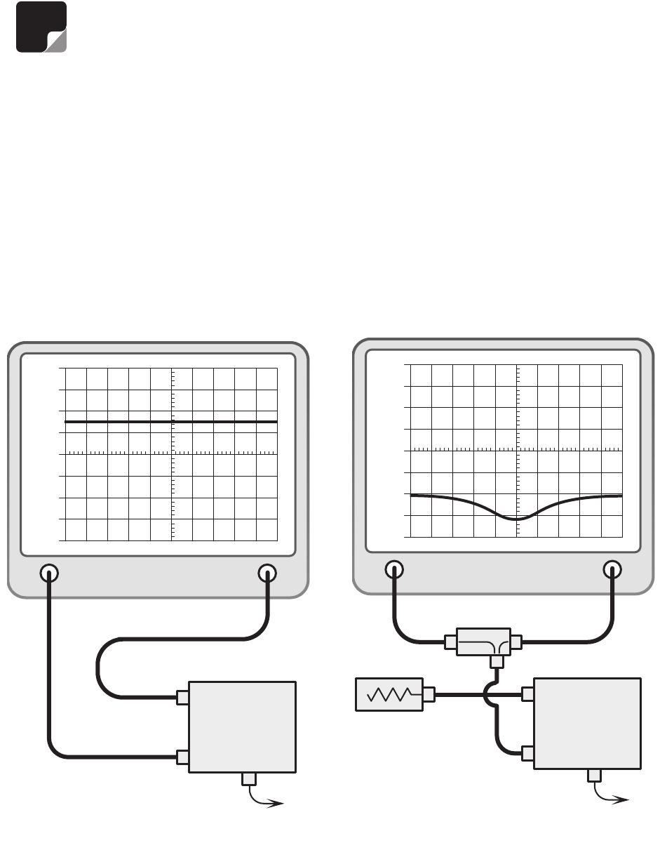
61-38-05 UserMan page 30 of 38
TXRX Systems Inc. Manual 7-9408-1.2 07/25/05 Page 30
5) Engage the Input Tuning Capacitors one at a
time and rotate them for maximum gain.
NOTE: If the gain peaks at a level
about 60% of maximum, one of the
variable capacitors should be rotated
180° and steps 4 and 5 repeated.
6)Connect the return loss bridge to
the tracking generator as shown in
Figure 22 but do not connect it to the
amplifier. Leave the test port on the
bridge open.
7) Set up the 0 dB return loss reference. For the
IFR A-7550 do the following procedure:
a) Make sure that the unit is in "LIVE" mode
when performing step 7.
b) From the Mode Menu, "STORE" the above
trace.
c) Switch to the Display Menu and select "REF".
The trace should appear at the 0 dB level.
8) Connect the bridge and load to the amplifier as
shown in figure 22 and see if the input return
loss is down -16 dB or more. If it is, skip to step
10.
9) Alternately adjust the input tuning capacitors for
increased return loss. A return loss of -20 to -30
dB loss should be obtained with maximum loss
at the center frequency.
10) Reverse the connections as shown in
Figure 23 and see if the output return loss is -
16 dB or more. If it is, skip to step 12.
11) Alternately adjust the output tuning capacitors
for increased return loss. It should be possible
to obtain -20 to -30 dB loss with maximum loss
at the center frequency.
NOTE
GENERATE
OUTPUT
ANALYZER
INPUT
+40
+30
+20
+10
0
-10
-20
-30
-40
BRIDGE
DC
AMPLIFIER
INPUT
OUTPUT
50 OHM
LOAD
Figure 22: Measuring input return loss.
GENERATE
OUTPUT
ANALYZER
INPUT
+40
+30
+20
+10
0
-10
-20
-30
-40
DC
AMPLIFIER
INPUT
OUTPUT
Figure 21: Measuring amplifier gain.
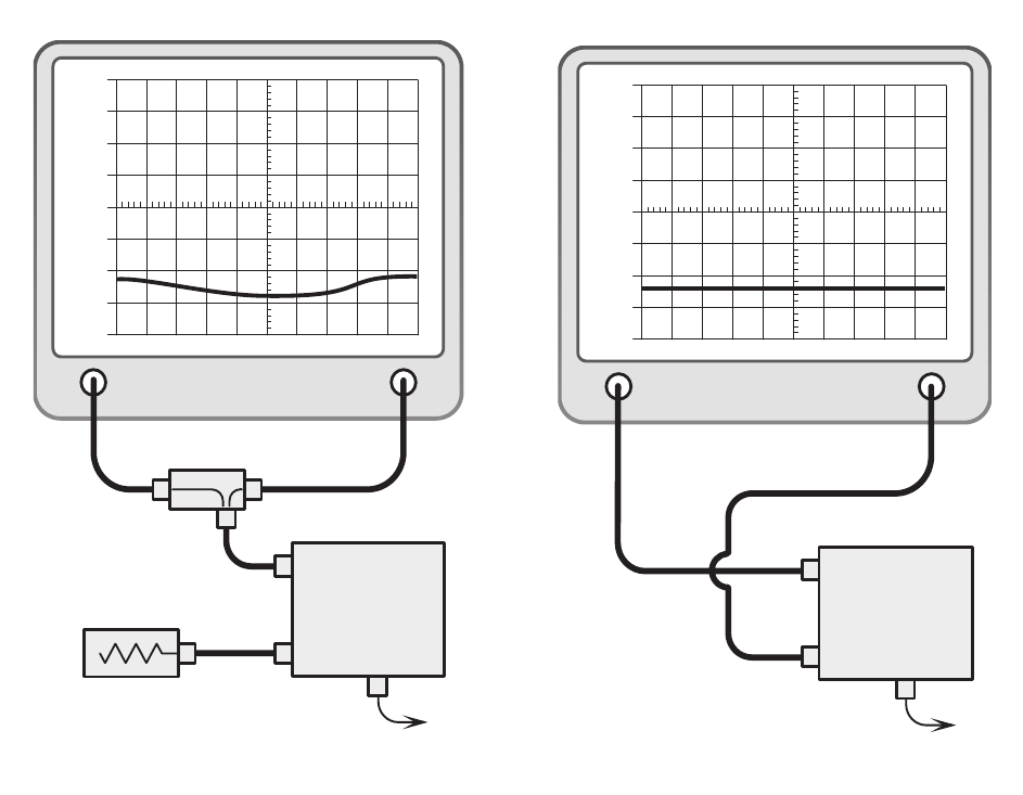
TXRX Systems Inc. Manual 7-9408-1.2 07/25/05 Page 31
61-38-05 UserMan page 31 of 38
12) Due to interaction, tuning the output circuitry
affects the input tuning and vise-versa. Repeat
steps 8 through 11 until acceptable input and
output return loss occurs without further tun-
ing.
13) Connect the equipment as shown in Figure 24
but connect the test leads together through a
female barrel connector and repeat the zero
reference procedure of step 2.
14) Using the figure 24 connection, verify that the
reverse isolation is at least -20 to -22 dB. This
value will occur normally as the result of proper
tuning.
The greater the reverse isolation the better as this
value must exceed the gain of the amplifier or oscil-
lation may occur. If after proper tuning this value
remains low, it may indicate a bad bypass capacitor
or defective RF transistor.
Output Level Control (OLC)
The OLC circuits are preset at the factory to limit
the RF power output of the signal booster branch to
the maximum two-carrier level as indicated on the
specification drawing. DO NOT attempt to adjust
or change this setting. This setting will be ade-
quate for protecting the final amplifier stage and
limiting intermodulation products.
OLC voltage data sheets are included with the
equipment shipment and list the actual OLC volt-
age values in relation to the degree of overload
detected for your unit. These sheets also record
the measured 1 dB compression point for the
branch and the calculated output intercept point
based on this compression point data.
CHECKING FOR OVERLOAD
Measurement of the DC voltage developed by the
OLC circuitry is a way to determine the degree of
input signal overload. In normal operation, up to 10
dB of overload on an intermittent basis is consid-
ered acceptable in most installations. Higher levels
GENERATE
OUTPUT
ANALYZER
INPUT
+40
+30
+20
+10
0
-10
-20
-30
-40
DC
AMPLIFIER
INPUT
OUTPUT
Figure 24: Measuring reverse isolation.
GENERATE
OUTPUT
ANALYZER
INPUT
+40
+30
+20
+10
0
-10
-20
-30
-40
DC
50 OHM
LOAD
BRIDGE
AMPLIFIER
INPUT
OUTPUT
Figure 23: Measuring output return loss.
61-38-05 UserMan page 32 of 38
TXRX Systems Inc. Manual 7-9408-1.2 07/25/05 Page 32
generally cause noticeable gain reductions to other
channels on the system and may also exceed the
maximum input level.
Connect the positive lead of a multimeter set to
measure DC voltage on a 0-20 volt scale, to the
OLC voltage test point on the OLC assembly. Fig-
ure 8 shows the location of the test point on the 3-
6280 OLC assembly. The negative lead of the mul-
timeter is connected to the chassis. (The black test
probe jacks on the voltage regulator assembly are
convenient for this). Compare the measured volt-
age readings with those on the OLC test data
sheet to see what degree of overload, if any, is tak-
ing place. Refer to the section in this manual titled
"Gain Reduction Methods" to correct an excessive
overload condition.
MAINTENANCE AND REPAIR
Signal boosters manufactured by TX RX Systems,
Inc. can function reliably for 10 or more years with
little or no maintenance. However, if the amplifiers
are subjected to excessively high signal levels,
power surges or lightning strikes, failures may
occur. The following procedures may be followed
for detecting a malfunctioning unit or as part of a
periodic maintenance program.
1) Heat sinks for the power amplifiers should be
cleared of dust and debris.
2) Inspect the units to see that the LED DC indica-
tors are lit (remove any dust or debris that may
obscure the LEDs). This will verify that DC
power is flowing properly. Check all hardware
for tightness.
3) Compare system performance to initial perfor-
mance levels measured when the system was
first installed. The lack of signal can be traced to
a malfunctioning amplifier by progressive signal
monitoring from the output (far end) to the input
end of the system noting the area where the
signal returns to normal level. The next amplifier
toward the output end of the system will proba-
bly be the one that failed.
or
Measure the gain of each branch at any conve-
nient frequency in the working frequency bands
to verify that the gain specifications are being
met. If the gain values fall below that specified
for a given model check the following:
A) Open the signal booster cabinet and inspect for
any loose or broken connections or cables, and
repair as necessary.
B) Measure the output of the power supply and
power regulators to see that the proper operat-
ing voltage is being maintained.
C) If the operating voltage is proper but the gain is
still low, measure the gain of each amplifier
stage until the one with low gain is isolated.
Replace a low gain amplifier with a new ampli-
fier stage to correct the problem.
RECOMMENDED REPLACEMENT PARTS
One each of the following: Power Amplifier Assem-
bly 3-11792, 1stg/3stg Amplifier Assembly 3-
11423, Voltage Regulator Assembly 3-5969, and
Power Supply Assembly 3-15503.
CONVERSION CHART
A Power in Watts to dBm conversion chart is
included on the following three pages. Most of the
setup and conversion procedures refer to power
levels in dBm more often than in Watts. This is
much more convenient when dealing with the
power levels and gain figures of signal boosters.
The chart allows easy conversion between the two
scales when necessary.
TXRX Systems Inc. Manual 7-9408-1.2 07/25/05 Page 33
61-38-05 UserMan page 33 of 38
61-38-05 Signal Booster Family Specifications by Part Number
------------------------------------------------------------------- Part Numbers -------------------------------------------------------------------
Specification 61-38-05331 61-38-05251 61-38-04401 61-38-04359
Frequency Range (MHz) 138 - 144 148 -174 148-174 138 - 144
Minimum Guard Band (MHz) 5.85 9 3.04 4.02
Number of Passbands 2222
Pass Bandwidth 150 KHz 1 MHz 1.) 1.965 MHz Single Channel
2.) Single Channel 1.56 MHz
Maximum Gain (dB) 88 88 88 88
Maximum Input Signal Level (dBm) -20 -20 -20 -20
Maximum Output Power (1 carrier)Watts +28 +28 +26 +27
Gain Set Method--fixed-pads (dB) -3 , -6, -10 -3 , -6, -10 -3 , -6, -10 -3 , -6, -10
Gain Adjust Range (dB) 0, -3, -6, -9, -10, -13, -16, -19 0, -3, -6, -9, -10, -13, -16, -19 0, -3, -6, -9, -10, -13, -16, -19 0, -3, -6, -9, -10, -13, -16, -19
1 dB Compression Point (dBm) 31 31 31 31
3rd Order Output IP (dBm) 39 39 39 39
Output RF Sampler (dB) -50 -50 -50 -50
System Noise Figure (dB) without pads 6.5 6.5 6.5 6.5
Operating Temperature Range (°C) -30 to +60 -30 to +60 -30 to +60 -30 to +60
Nominal Impedance (ohms) 50 50 50 50
VSWR 2.0 : 1 2.0 : 1 2.0 : 1 2.0 : 1
Input / Output Connectors Type 'N' female Type 'N' female Type 'N' female Type 'N' female
RF Sampler Port Connectors BNC female BNC female BNC female BNC female
AC Input Voltage (VAC) 100-120 / 200-240 @ 50/60 Hz 100-120 / 200-240 @ 50/60 Hz 100-120 / 200-240 @ 50/60 Hz 100-120 / 200-240 @ 50/60 Hz
DC Backup Input Voltage (VDC) 24 - 29 VDC 24 - 29 VDC 24 - 29 VDC 24 - 29 VDC
Unit Current Drain 2 Amps DC, <0.5 Amps AC 2 Amps DC, <0.5 Amps AC 2 Amps DC, <0.5 Amps AC 2 Amps DC, <0.5 Amps AC
Housing G1: Painted Steel to NEMA 4 G1: Painted Steel to NEMA 4 G1: Painted Steel to NEMA 4 G1: Painted Steel to NEMA 4
G2: Stainless Steel to NEMA 4X G2: Stainless Steel to NEMA 4X G2: Stainless Steel to NEMA 4X G2: Stainless Steel to NEMA 4X
Nominal Size (in./ mm) 24 x 20 x 10 (610 x 508 x 254) 24 x 20 x 10 (610 x 508 x 254) 14 x 19 x 23 (356 x 483 x 585) 36 x 30 x 12 (915 x 762 x 305)
Net Weight (Lbs / Kg) 70 (31) 70 (31) 50 (23) 220 (96)
61-38-05 UserMan page 34 of 38
TXRX Systems Inc. Manual 7-9408-1.2 07/25/05 Page 34
61-38-05 Signal Booster Family Specifications by Part Number
---------------------------------------------- Part Numbers ----------------------------------------------
Specification 61-38-03324 61-38-04742 61-38-04744
Frequency Range (MHz) 138 - 144 138 - 144 138 - 144
Minimum Guard Band (MHz) 4.21 3 2.805
Number of Passbands 222
Pass Bandwidth 500 KHz/1.0 MHz 1.0 MHz Max 1.185 MHz
1.0 MHz 900 KHz/150 KHz
Maximum Gain (dB) 88 88 88
Maximum Input Signal Level (dBm) -20 -20 -20
Maximum Output Power (1 carrier) Watts +26 +26 +26
Gain Set Method--fixed-pads (dB) -3 , -6, -10 -3 , -6, -10 -3 , -6, -10
Gain Adjust Range (dB) 0, -3, -6, -9, -10, -13, -16, -19 0, -3, -6, -9, -10, -13, -16, -19 0, -3, -6, -9, -10, -13, -16, -19
1 dB Compression Point (dBm) 31 31 31
3rd Order Output IP (dBm) 39 39 39
Output RF Sampler (dB) -50 -50 -50
System Noise Figure (dB) (without pads) 6.5 6.5 6.5
Operating Temperature Range (°C) -30 to +60 -30 to +60 -30 to +60
Nominal Impedance (ohms) 50 50 50
VSWR 2.0 : 1 2.0 : 1 2.0 : 1
Input / Output Connectors Type 'N' female Type 'N' female Type 'N' female
RF Sampler Port Connectors BNC female BNC female BNC female
AC Input Voltage (VAC) 100-120 / 200-240 @ 50/60 Hz 100-120 / 200-240 @ 50/60 Hz 100-120 / 200-240 @ 50/60 Hz
DC Backup Input Voltage (VDC) 24 - 29 VDC 24 - 29 VDC 24 - 29 VDC
Unit Current Drain 2 Amps DC, <0.5 Amps AC 2 Amps DC, <0.5 Amps AC 2 Amps DC, <0.5 Amps AC
Housing G1: Painted Steel to NEMA 4 G1: Painted Steel to NEMA 4 G1: Painted Steel to NEMA 4
G2: Stainless Steel to NEMA 4X G2: Stainless Steel to NEMA 4X G2: Stainless Steel to NEMA 4X
Nominal Size (in./ mm) 30 x 20 x 8 (762 x 508 x 203) 30 x 20 x 8 (762 x 508 x 203) 30 x 20 x 8 (762 x 508 x 203)
Net Weight (Lbs / Kg) 75 (33) 75 (33) 75 (33)

TXRX Systems Inc. Manual 7-9408-1.2 07/25/05 Page 35
61-38-05 UserMan page 35 of 38
dBm dBw Watts Volts (50Ω)
80 50 100000 2236.07
79 49 79432.82 1992.9
78 48 63095.74 1776.17
77 47 50118.72 1583.01
76 46 39810.72 1410.86
75 45 31622.78 1257.43
74 44 25118.86 1120.69
73 43 19952. 62 998.81
72 42 15848.93 890.19
71 41 12589.25 793.39
70 40 10000 707.11
69 39 7943.28 630.21
68 38 6309.57 561.67
67 37 5011.87 500.59
66 36 3981.07 446.15
65 35 3162.28 397.64
64 34 2511.89 354.39
63 33 1995.26 315.85
62 32 1584.89 281.5
61 31 1258.93 250.89
60 30 1000 223.61
59 29 794.33 199.29
58 28 630.96 177.62
57 27 501.19 158.3
56 26 398.11 141.09
55 25 316.23 125.74
54 24 251.19 112.07
53 23 199.53 99.88
52 22 158.49 89.02
51 21 125.89 79.34
50 20 100 70.71
49 19 79.43 63.02
48 18 63.1 56.17
47 17 50.12 50.06
46 16 39.81 44.62
45 15 31.62 39.76
44 14 25.12 35.44
43 13 19.95 31.59
42 12 15.85 28.15
41 11 12.59 25.09
dBm dBw Watts Volts (50Ω)
40 10 10 22.36
39 9 7.94 19.93
38 8 6.31 17.76
37 7 5.01 15.83
36 6 3.98 14.11
35 5 3.16 12.57
34 4 2.51 11.21
33 3 2 9.99
32 2 1.59 8.9
31 1 1.26 7.93
30 0 1 7.07
29 -1 0.79 6.3
28 -2 0.63 5.62
27 -3 0.5 5.01
26 -4 0.4 4.46
25 -5 0.32 3.98
24 -6 0.25 3.54
23 -7 0.2 3.16
22 -8 0.16 2.82
21 -9 0.13 2.51
20 -10 0.1 2.24
19 -11 0.08 1.99
18 -12 0.06 1.78
17 -13 0.05 1.58
16 -14 0.04 1.41
15 -15 0.03 1.26
14 -16 0.03 1.12
13 -17 0.02 1
12 -18 0.02 0.89
11 -19 0.01 0.79
10 -20 0.01 0.71
9 -21 0.01 0.63
8 -22 0.01 0.56
7 -23 0.01 0.5
6-2400.45
5-250 0.4
4-2600.35
3-2700.32
2-2800.28
1-2900.25
Power Conversion Chart
dBm to dBw: Watts: Microvolts

61-38-05 UserMan page 36 of 38
TXRX Systems Inc. Manual 7-9408-1.2 07/25/05 Page 36
dBm dBw Watts uVolts (50Ω)
0 -30 1.0000E-03 223606.8
-1 -31 7.9433E-04 199289.77
-2 -32 6.3096E-04 177617.19
-3 -33 5.0119E-04 158301.49
-4 -34 3.9811E-04 141086.35
-5 -35 3.1623E-04 125743.34
-6 -36 2.5119E-04 112068.87
-7 -37 1.9953E-04 99881.49
-8 -38 1.5849E-04 89019.47
-9 -39 1.2589E-04 79338.69
-10 -40 1.0000E-04 70710.68
-11 -41 7.9433E-05 63020.96
-12 -42 6.3096E-05 56167.49
-13 -43 5.0119E-05 50059.33
-14 -44 3.9811E-05 44615.42
-15 -45 3.1623E-05 39763.54
-16 -46 2.5119E-05 35439.29
-17 -47 1.9953E-05 31585.3
-18 -48 1.5849E-05 28150.43
-19 -49 1.2589E-05 25089.1
-20 -50 1.0000E-05 22360.68
-21 -51 7.9433E-06 19928.98
-22 -52 6.3096E-06 17761.72
-23 -53 5.0119E-06 15830.15
-24 -54 3.9811E-06 14108.64
-25 -55 3.1623E-06 12574.33
-26 -56 2.5119E-06 11206.89
-27 -57 1.9953E-06 9988.15
-28 -58 1.5849E-06 8901.95
-29 -59 1.2589E-06 7933.87
-30 -60 1.0000E-06 7071.07
-31 -61 7.9433E-07 6302.1
-32 -62 6.3096E-07 5616.75
-33 -63 5.0119E-07 5005.93
-34 -64 3.9811E-07 4461.54
-35 -65 3.1623E-07 3976.35
-36 -66 2.5119E-07 3543.93
-37 -67 1.9953E-07 3158.53
-38 -68 1.5849E-07 2815.04
-39 -69 1.2589E-07 2508.91
dBm dBw Watts uVolts (50Ω)
-40 -70 1.0000E-07 2236.07
-41 -71 7.9433E-08 1992.9
-42 -72 6.3096E-08 1776.17
-43 -73 5.0119E-08 1583.02
-44 -74 3.9811E-08 1410.86
-45 -75 3.1623E-08 1257.43
-46 -76 2.5119E-08 1120.69
-47 -77 1.9953E-08 998.82
-48 -78 1.5849E-08 890.2
-49 -79 1.2589E-08 793.39
-50 -80 1.0000E-08 707.11
-51 -81 7.9433E-09 630.21
-52 -82 6.3096E-09 561.68
-53 -83 5.0119E-09 500.59
-54 -84 3.9811E-09 446.15
-55 -85 3.1623E-09 397.64
-56 -86 2.5119E-09 354.39
-57 -87 1.9953E-09 315.85
-58 -88 1.5849E-09 281.5
-59 -89 1.2589E-09 250.89
-60 -90 1.0000E-09 223.61
-61 -91 7.9433E-10 199.29
-62 -92 6.3096E-10 177.62
-63 -93 5.0119E-10 158.3
-64 -94 3.9811E-10 141.09
-65 -95 3.1623E-10 125.74
-66 -96 2.5119E-10 112.07
-67 -97 1.9953E-10 99.88
-68 -98 1.5849E-10 89.02
-69 -99 1.2589E-10 79.34
-70 -100 1.0000E-10 70.71
-71 -101 7.9433E-11 63.02
-72 -102 6.3096E-11 56.17
-73 -103 5.0119E-11 50.06
-74 -104 3.9811E-11 44.62
-75 -105 3.1623E-11 39.76
-76 -106 2.5119E-11 35.44
-77 -107 1.9953E-11 31.59
-78 -108 1.5849E-11 28.15
-79 -109 1.2589E-11 25.09
Power Conversion Chart
dBm to dBw: Watts: Microvolts

TXRX Systems Inc. Manual 7-9408-1.2 07/25/05 Page 37
61-38-05 UserMan page 37 of 38
dBm dBw Watts uVolts (50Ω)
-80 -110 1.0000E-11 22.36
-81 -111 7.9433E-12 19.93
-82 -112 6.3096E-12 17.76
-83 -113 5.0119E-12 15.83
-84 -114 3.9811E-12 14.11
-85 -115 3.1623E-12 12.57
-86 -116 2.5119E-12 11.21
-87 -117 1.9953E-12 9.99
-88 -118 1.5849E-12 8.9
-89 -119 1.2589E-12 7.93
-90 -120 1.0000E-12 7.07
-91 -121 7.9433E-13 6.3
-92 -122 6.3096E-13 5.62
-93 -123 5.0119E-13 5.01
-94 -124 3.9811E-13 4.46
-95 -125 3.1623E-13 3.98
-96 -126 2.5119E-13 3.54
-97 -127 1.9953E-13 3.16
-98 -128 1.5849E-13 2.82
-99 -129 1.2589E-13 2.51
-100 -130 1.0000E-13 2.24
-101 -131 7.9433E-14 1.99
-102 -132 6.3096E-14 1.78
-103 -133 5.0119E-14 1.58
-104 -134 3.9811E-14 1.41
-105 -135 3.1623E-14 1.26
-106 -136 2.5119E-14 1.12
-107 -137 1.9953E-14 1
-108 -138 1.5849E-14 0.89
-109 -139 1.2589E-14 0.79
-110 -140 1.0000E-14 0.71
-111 -141 7.9433E-15 0.63
-112 -142 6.3096E-15 0.56
-113 -143 5.0119E-15 0.5
-114 -144 3.9811E-15 0.45
-115 -145 3.1623E-15 0.4
-116 -146 2.5119E-15 0.35
-117 -147 1.9953E-15 0.32
-118 -148 1.5849E-15 0.28
-119 -149 1.2589E-15 0.25
dBm dBw Watts uVolts (50Ω)
-120 -150 1.0000E-15 0.22
-121 -151 7.9433E-16 0.2
-122 -152 6.3096E-16 0.18
-123 -153 5.0119E-16 0.16
-124 -154 3.9811E-16 0.14
-125 -155 3.1623E-16 0.13
-126 -156 2.5119E-16 0.11
-127 -157 1.9953E-16 0.1
-128 -158 1.5849E-16 0.09
-129 -159 1.2589E-16 0.08
-130 -160 1.0000E-16 0.07
-131 -161 7.9433E-17 0.06
-132 -162 6.3096E-17 0.06
-133 -163 5.0119E-17 0.05
-134 -164 3.9811E-17 0.05
-135 -165 3.1623E-17 0.04
-136 -166 2.5119E-17 0.04
-137 -167 1.9953E-17 0.03
-138 -168 1.5849E-17 0.03
-139 -169 1.2589E-17 0.03
-140 -170 1.0000E-17 0.02
-141 -171 7.9433E-18 0.02
-142 -172 6.3096E-18 0.02
-143 -173 5.0119E-18 0.02
-144 -174 3.9811E-18 0.01
-145 -175 3.1623E-18 0.01
-146 -176 2.5119E-18 0.01
-147 -177 1.9953E-18 0.01
-148 -178 1.5849E-18 0.01
-149 -179 1.2589E-18 0.01
-150 -180 1.0000E-18 0.01
Power Conversion Chart
dBm to dBw: Watts: Microvolts
61-38-05 UserMan page 38 of 38
TXRX Systems Inc. Manual 7-9408-1.2 07/25/05 Page 38
NOTES