Bwave Technology TETHYS Tethys User Manual revised
Shanghai Bwave Technology Co.,Ltd. Tethys Users Manual revised
Contents
- 1. Users Manual
- 2. Users Manual revised
Users Manual revised
All information contained in these materials, including products and product specifications,
represents information on the product at the time of publication and is subject to change by
Renesas Electronics Corp. without notice. Please review the latest information published by
Renesas Electronics Corp.
RTK00V2XRC7746SFS
User’s Manual: Hardware
Rev.1.3 September. 2017
ASD-B-16-0247

Hardware Design Specification
ASD-B-16-0247 Rev1.3 Page
2
of 105
September 8, 2017
RTK00V2XRC7746SFS
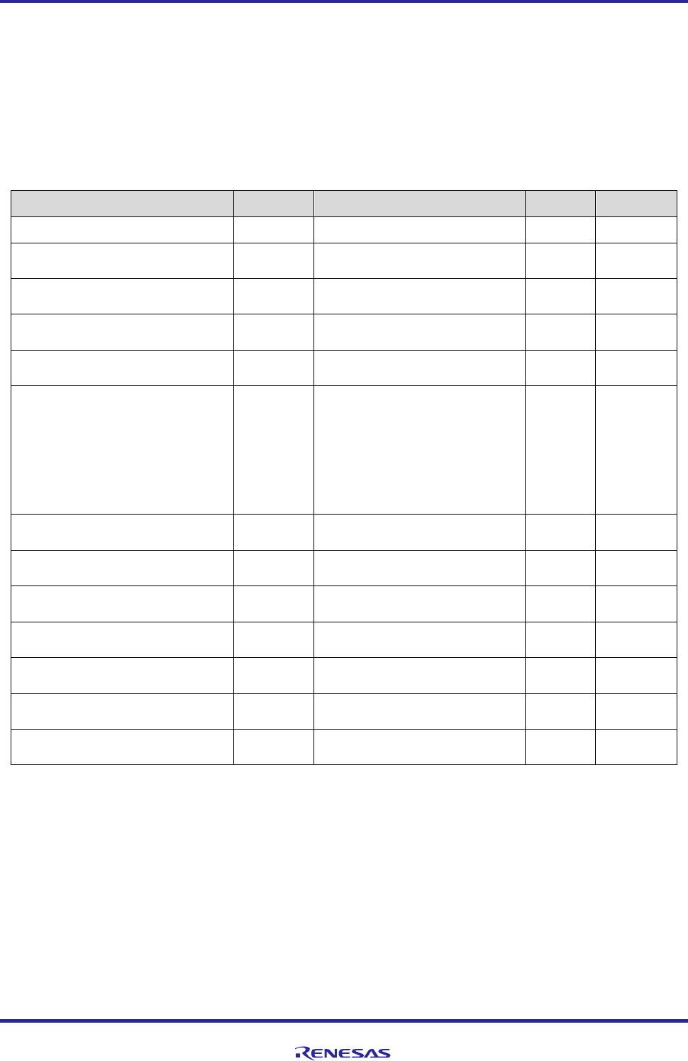
CONTENTS
1 OVERVIEW ..........................................................................................................................................9
1.1 FEATURES ............................................................................................................................................ 10
1.1.1 Features of the Tethys Board
..................................................................................................... 10
1.1.2 Functions of the Tethys Board
.................................................................................................... 11
1.2 USAGE NOTES ...................................................................................................................................... 12
1.2.1 Specifications of the Tethys Board
............................................................................................. 12
1.3 BOARD CONFIGURATION ....................................................................................................................... 13
1.3.1 Block Diagram of the Tethys Board
........................................................................................... 13
2 OPERATING CONDITION AND ANTENNA CHARACTERISTIC ....................................................... 14
2.1 OPERATING CONDITION ......................................................................................................................... 14
3 SPECIFICATIONS OF INTERFACE MODULES ON THE TETHYS BOARD ....................................... 15
3.1 MODE SETTING .................................................................................................................................... 15
3.1.1 Specifications
............................................................................................................................. 15
3.1.2 MD0 Pin -Selection of Free-Running Mode or Step-Up Mode
.................................................. 15
3.1.3 MD [3:1] Pins-Selection of Boot Device
..................................................................................... 15
3.1.4 MD4 Pin-Selection of CS0 Space Size
...................................................................................... 15
3.1.5 MD5 Pin-Reserved
..................................................................................................................... 15
3.1.6 MD [7:6] Pins-Selection of Master Boot Processor
................................................................... 15
3.1.7 MD8 Pin-Selection of Area 0 Space Data Bus Width
................................................................ 16
3.1.8 MD9 Pin-Selection of Crystal Resonator or Crystal Oscillator
................................................... 16
3.1.9 MD21, MD20, MD11, MD10, and MDT [1:0] Pins-Switching of JTAG, SDHI1, and SDHI2
....... 16
3.1.10 MD [14:13] Pins-Frequency Mode Setting
................................................................................. 17
3.1.11 Initial Values of Mode Setting Pins on Tethys Board
................................................................. 17
3.2 DDR3-SDRAM INTERFACE (DBSC) ...................................................................................................... 17
3.2.1 Specifications
............................................................................................................................. 17
3.2.2 Signal Connections between R-Car W2H and DDR3-SDRAMs
................................................ 18
3.2.3 Block Diagram
............................................................................................................................ 19
3.3 SPI-FLASH INTERFACE (QSPI) ............................................................................................................... 20
3.3.1 Specifications
............................................................................................................................. 20
3.3.2 Block Diagram
............................................................................................................................ 20
3.4 AUDIO CODEC INTERFACES (SSI0, SSI1) ................................................................................................ 21
3.4.1 Specifications
............................................................................................................................. 21
3.4.2 Block Diagram
............................................................................................................................ 21
3.5 EMMC MEMORY INTERFACE (EMMC) ................................................................................................... 22
3.5.1 Specifications
............................................................................................................................. 22

Hardware Design Specification
ASD-B-16-0247 Rev1.3 Page
3
of 105
September 8, 2017
RTK00V2XRC7746SFS
3.5.2 Block Diagram
............................................................................................................................ 22
3.6 SD CARD HOST INTERFACE (SDHI2) ...................................................................................................... 23
3.6.1 Specifications
............................................................................................................................. 23
3.6.2 Block Diagram
............................................................................................................................ 23
3.7 MINI PCI EXPRESS INTERFACE ............................................................................................................... 24
3.7.1 Specifications
............................................................................................................................. 24
3.7.2 The Mini PCIE connector signal configuration are shown as below:
......................................... 24
3.7.3 Block Diagram
............................................................................................................................ 28
3.8 USB TO UART ..................................................................................................................................... 29
3.8.1 Specifications
............................................................................................................................. 29
3.8.2 Block Diagram
............................................................................................................................ 29
3.9 USB2.0 INTERFACE .............................................................................................................................. 30
3.9.1 Specifications
............................................................................................................................. 30
3.9.2 Block Diagram
............................................................................................................................ 31
3.10 DEBUG INTERFACE ............................................................................................................................... 32
3.10.1 CPU debug
................................................................................................................................. 32
3.10.2 CPU JTAG2 debug
..................................................................................................................... 33
3.10.3 MCU debug
................................................................................................................................ 34
3.11 GYRO/G-SENSOR.............................................................................................................................. 35
3.11.1 Specifications
............................................................................................................................. 35
3.11.2 Block Diagram
............................................................................................................................ 35
3.12 I2C INTERFACES ................................................................................................................................... 36
3.12.1 Specifications
............................................................................................................................. 36
3.12.2 List of Slave Addresses
.............................................................................................................. 37
3.12.3 Block Diagram
............................................................................................................................ 37
3.13 GPS MODULE ...................................................................................................................................... 38
3.13.1 Specifications
............................................................................................................................. 38
3.13.2 Block Diagram
............................................................................................................................ 38
3.14 CAN AND FLEXRAY INTERFACE ............................................................................................................. 39
3.14.1 Specifications
............................................................................................................................. 39
3.14.2 Block Diagram
............................................................................................................................ 39
3.15 LEDS AND SWITCHES ........................................................................................................................... 41
3.15.1 Specifications
............................................................................................................................. 41
3.16 CONNECTION BETWEEN CPU AND MCU ................................................................................................. 44
3.16.1 Specifications
............................................................................................................................. 44
3.16.2 Block Diagram
............................................................................................................................ 44
3.17 CLOCK SYSTEM .................................................................................................................................... 45
3.17.1 Clock Signals Supplied to the R-Car W2H
................................................................................ 45
3.17.2 Differential Clock Signals Supplied to the R-Car W2H
.............................................................. 45

Hardware Design Specification
ASD-B-16-0247 Rev1.3 Page
4
of 105
September 8, 2017
RTK00V2XRC7746SFS
3.17.3 Clock Signals Supplied to Devices Other than R-Car W2H
...................................................... 45
3.17.4 Block Diagram
............................................................................................................................ 46
3.18 EXTERNAL INTERRUPTS ........................................................................................................................ 47
3.18.1 Specifications
............................................................................................................................. 47
3.18.2 Block Diagram
............................................................................................................................ 47
3.19 RESET SYSTEM ..................................................................................................................................... 48
3.19.1 Specifications
............................................................................................................................. 48
3.19.2 Block Diagram
............................................................................................................................ 48
3.19.3 Reset Sequence
........................................................................................................................ 49
3.20 POWER SYSTEM .................................................................................................................................... 50
3.20.1 Specifications
............................................................................................................................. 50
3.20.2 Block Diagram
............................................................................................................................ 51
3.20.3 Power Sequence
........................................................................................................................ 52
4 MEMORY MAP ................................................................................................................................... 53
4.1 SPECIFICATIONS ................................................................................................................................... 53
4.2 FUNCTION ........................................................................................................................................... 57
4.2.1 Control the power of the Tethys Custom Board.
........................................................................ 57
4.2.2 Realize the UART with the baud rate of 115200
........................................................................ 58
4.2.3 Realize an asynchronous serial with baud rate of 1M between RH850 and CPU.
................... 59
4.2.4 Make CAN0 and CAN1 working with baud rate of 1M
............................................................... 59
5 OUTLINE DIAGRAMS OF THE TETHYS BOARD .............................................................................. 60
5.1 TETHYS BOARD DIMENSION ................................................................................................................... 60
5.2 THE WEIGHT OF THE TETHYS BOARD ...................................................................................................... 60
5.3 TETHYS ID DIMENSION ......................................................................................................................... 61
5.4 TETHYS ASSEMBLY ............................................................................................................................... 63
6 BOARD CONNECTORS ...................................................................................................................... 67
6.1 TOP SIDE CONNECTORS ......................................................................................................................... 67
6.2 BOTTOM SIDE CONNECTORS ................................................................................................................... 68
6.3 THE DETAILS OF CONNECTORS ............................................................................................................... 69
7 APPENDIX .......................................................................................................................................... 71
7.1 USB DEBUG CABLE .............................................................................................................................. 71
7.2 AC ADAPTER ....................................................................................................................................... 72
7.2.1 Specifications
............................................................................................................................. 72
7.2.2 Mechanic Size and Picture
........................................................................................................ 73
7.3 GPS ANTENNA ..................................................................................................................................... 75
7.3.1 Specification
............................................................................................................................... 75

Hardware Design Specification
ASD-B-16-0247 Rev1.3 Page
5
of 105
September 8, 2017
RTK00V2XRC7746SFS
7.4 V2X ANTENNA1 WITH 2M CABLE ........................................................................................................... 77
7.4.1 Specification
............................................................................................................................... 77
7.5 V2X ANTENNA (ROD TYPE) .................................................................................................................. 84
7.5.1 Specification
............................................................................................................................... 84
7.6 RF CABLE ........................................................................................................................................... 91
7.6.1 Specification
............................................................................................................................... 91
7.7 JTAG DEBUG BOARD WITH FPC CABLE ................................................................................................. 92
7.7.1 Specifications
............................................................................................................................. 92
7.7.2 Block Structure
........................................................................................................................... 92
7.7.3 Block Diagram
............................................................................................................................ 93
7.8 V2X CONNECTION BOARD ..................................................................................................................... 94
7.8.1 Board Structure
.......................................................................................................................... 94
7.8.2 Block Diagram
............................................................................................................................ 95
7.8.3 Block dimension
........................................................................................................................... 95
7.9 SUB BOARD TORTUGA WIRELESS MODULE BOARD DIMENSION ................................................................... 96
7.9.1 RF characteristic
........................................................................................................................ 96
7.9.2 Board Dimension
....................................................................................................................... 98
7.10 SIDE COVER OPTION OF CASE ............................................................................................................... 100
7.11 ACRONYMS AND ABBREVIATIONS ........................................................................................................ 101
8 REGULATORY WARNING STATEMENTS ........................................................................................ 102
9 EU DECLARATION OF CONFORMITY (DOC) ................................................................................. 104
10 MANUFACTURER INFORMATION.................................................................................................. 105
WEBSITE AND SUPPORT ....................................................................................................................... 106
NOTICE ................................................................................................................................................... 108

Hardware Design Specification
ASD-B-16-0247 Rev1.3 Page
6
of 105
September 8, 2017
RTK00V2XRC7746SFS
Tables
Table 1 Features of the Tethys Board .......................................................................................................... 10
Table 2 List of Tethys Board Functions ....................................................................................................... 11
Table 3 Operating Condition...................................................................................................................... 14
Table 4 DDR3-SDRAM Interface Specifications ......................................................................................... 18
Table 5 Signal Connections between R-Car W2H and DDR3-SDRAMs ........................................................ 18
Table 6 SPI-Flash Interface Specifications .................................................................................................. 20
Table 7 SSI Codec Specifications ............................................................................................................... 21
Table 8 eMMC Memory Interface (eMMC) Specifications........................................................................... 22
Table 9 Specifications of SD Card Host Interface (SDHI2) .......................................................................... 23
Table 10 USB to UART Specifications ....................................................................................................... 29
Table 11 USB2.0 Interface ........................................................................................................................ 30
Table 12 CPU debug Specifications ........................................................................................................... 32
Table 13 CPU JTAG2 debug ..................................................................................................................... 33
Table 14 MCU debug Specification............................................................................................................ 34
Table 15 GYRO/G-SENSOR Specifications ............................................................................................... 35
Table 16 List of I2C Devices ..................................................................................................................... 36
Table 17 List of I2C Slave Addresses ......................................................................................................... 37
Table 18 CAN and Flexray Interface Specifications ..................................................................................... 39
Table 19 DIP Switches default setting is as below table ............................................................................... 41
Table 20 Slide Switches default setting is as below table: ............................................................................. 43
Table 21 List of Clock Signals and Crystals for the R-Car W2H ................................................................... 45
Table 22 List of Differential Clock Signals Supplied to the R-Car W2H ........................................................ 45
Table 23 List of Clocks and Crystals other than for R-Car W2H ................................................................... 45
Table 24 External Interrupts Specifications ................................................................................................. 47
Table 25 Reset System Specifications......................................................................................................... 48
Table 26 List of the Switching Controllers and Regulators on the Tethys Board ............................................. 50
Table 27 Antenna Specification for GPS module ......................................................................................... 75
Table 28 Antenna Specification for V2X (2m cable) .................................................................................... 77
Table 29 Antenna Specification for V2X (Rod Type) ................................................................................... 84
Table 30 RF Cable Specification for GPS module & RF Board..................................................................... 91

Hardware Design Specification
ASD-B-16-0247 Rev1.3 Page
7
of 105
September 8, 2017
RTK00V2XRC7746SFS
Figures
Figure 1 Block Diagram of the Tethys Board .............................................................................................. 13
Figure 2 Block Diagram of the DDR3-SDRAM Interface ............................................................................ 19
Figure 3 Block Diagram of the SPI-Flash Interface ..................................................................................... 20
Figure 4 Block Diagram of the Audio Codec Interface ................................................................................. 21
Figure 5 Block Diagram of the eMMC Memory Interface ............................................................................ 22
Figure 6 Block Diagram of the SDHI2 Interface ......................................................................................... 23
Figure 7 Block Diagram of Mini PCI Express Interface ............................................................................... 28
Figure 8 Block Diagram of the USB to UART ............................................................................................ 29
Figure 9 Block Diagram of the USB2.0 Interface ........................................................................................ 31
Figure 10 Block Diagram of the CPU debug ............................................................................................... 32
Figure 11 Block Diagram of the CPU JTAG2 (SH-4AL) debug .................................................................... 33
Figure 12 Block Diagram of the MCU debug .............................................................................................. 34
Figure 13 Block Diagram of the GYRO/G-SENSOR ................................................................................... 35
Figure 14 Block Diagram of the I2C Interfaces ........................................................................................... 37
Figure 15 Block Diagram of the GPS module ............................................................................................. 38
Figure 16 Block Diagram of the CAN and Flexray Interface ........................................................................ 39
Figure 17 Block Diagram of the Connection between CPU and MCU ........................................................... 44
Figure 18 Block Diagram of the Clock system ............................................................................................ 46
Figure 19 Block Diagram of the External Interrupts .................................................................................... 47
Figure 20 Block Diagram of the Reset System ............................................................................................ 48
Figure 21 The Reset Sequence ................................................................................................................... 49
Figure 22 Block Diagram of the Power System ........................................................................................... 51
Figure 23 The Power Sequence.................................................................................................................. 52
Figure 24 The Tethys board dimension ....................................................................................................... 60
Figure 25 TOP Side Connectors ................................................................................................................. 67
Figure 26 Bottom side connectors .............................................................................................................. 68
Figure 27 Image of USB debug cable ......................................................................................................... 71
Figure 28 Power Adapter ID LOG specification .......................................................................................... 74
Figure 29 Image of Power Adapter ............................................................................................................. 74
Figure 30 Image of GPS Antenna from Bottom view ................................................................................... 76
Figure 31 Image of GPS Antenna from Top view ........................................................................................ 76
Figure 32 V2X Antenna Test Chamber description ...................................................................................... 78
Figure 33 V2X Antennal test axis definition description .............................................................................. 79
Figure 34 V2X Antennal VSWR test character ............................................................................................ 80
Figure 35 V2X Antennal 2D radiation pattern ............................................................................................. 81
Figure 36 V2X Antennal 3D radiation pattern ............................................................................................. 82
Figure 37 Image of V2X Antenna1 from Bottom view ................................................................................. 83
Figure 38 Image of V2X Antenna1 from Top view ...................................................................................... 83

Hardware Design Specification
ASD-B-16-0247 Rev1.3 Page
8
of 105
September 8, 2017
RTK00V2XRC7746SFS
Figure 39 V2X Antenna2 Test Chamber description .................................................................................... 85
Figure 40 V2X Antenna2 test axis definition description .............................................................................. 86
Figure 41 V2X Antenna2 VSWR test character ........................................................................................... 87
Figure 42 V2X Antenna2 2D radiation pattern ............................................................................................ 88
Figure 43 V2X Antenna2 3D radiation pattern ............................................................................................ 89
Figure 44 Image of V2X Antenna2 (SMA rotate 90 degree) ......................................................................... 90
Figure 45 Image of V2X Antenna2 (SMA rotate 0 degree) ........................................................................... 90
Figure 46 RF Cable .................................................................................................................................. 91
Figure 47 JTAG Debug Board with FPC Cable for R-CAR W2H & RH850 MCU ......................................... 92
Figure 48 JTAG Debug Board block structure ............................................................................................. 92
Figure 49 Block Diagram of the JTAG Debug Board ................................................................................... 93
Figure 50 Top side view of V2X Connection board ..................................................................................... 94
Figure 51 Bottom side view of V2X Connection board ................................................................................ 94
Figure 52 Block structure of V2X Connection board ................................................................................... 94
Figure 53 Block Diagram of the V2X Connection board .............................................................................. 95
Figure 54 Side cover option of case ......................................................................................................... 100
Appendix
Appendix 1 Acronyms and Abbreviations ................................................................................................. 101
Hardware Design Specification
ASD-B-16-0247 Rev1.3 Page
9
of 105
September 8, 2017
RTK00V2XRC7746SFS
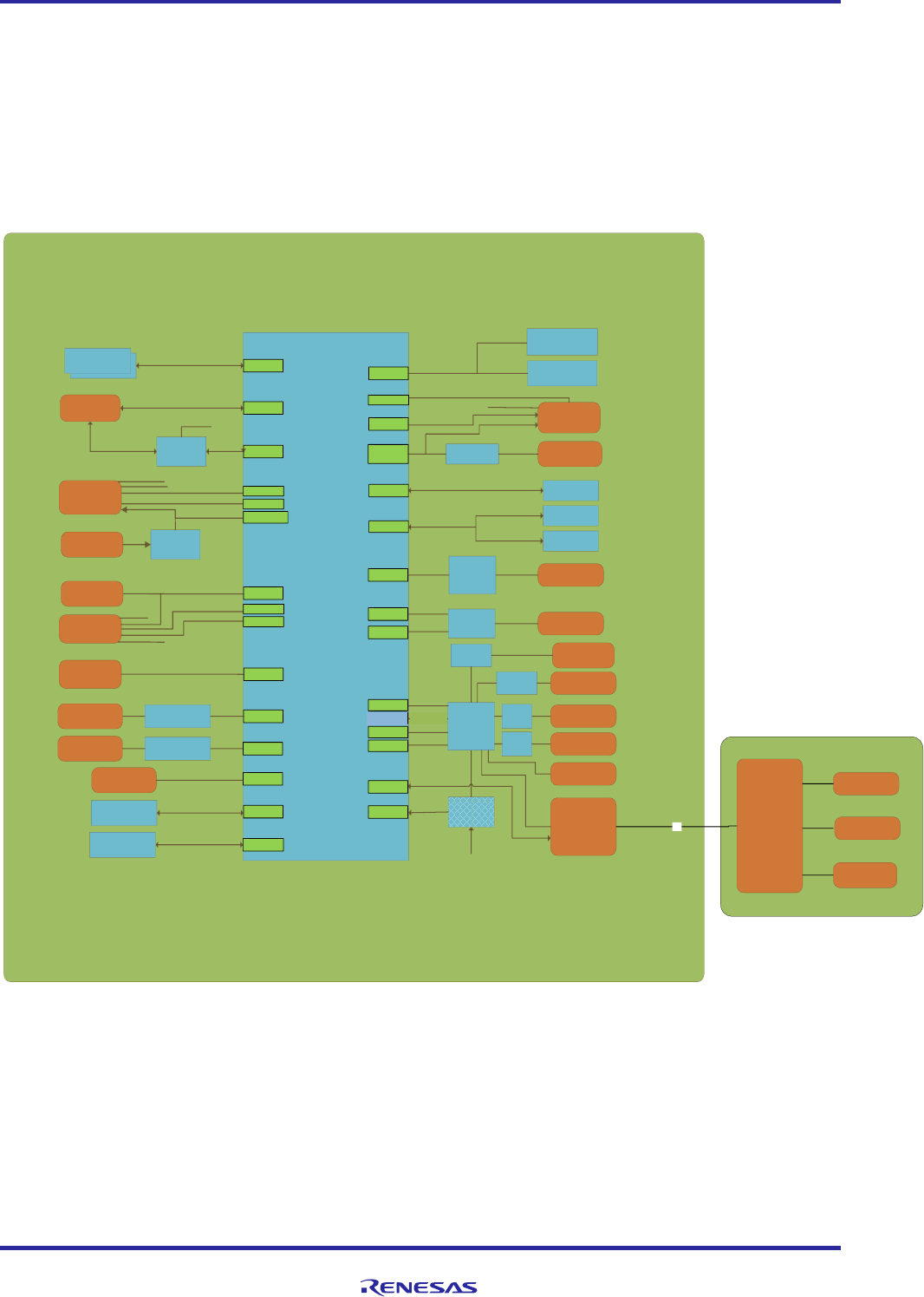
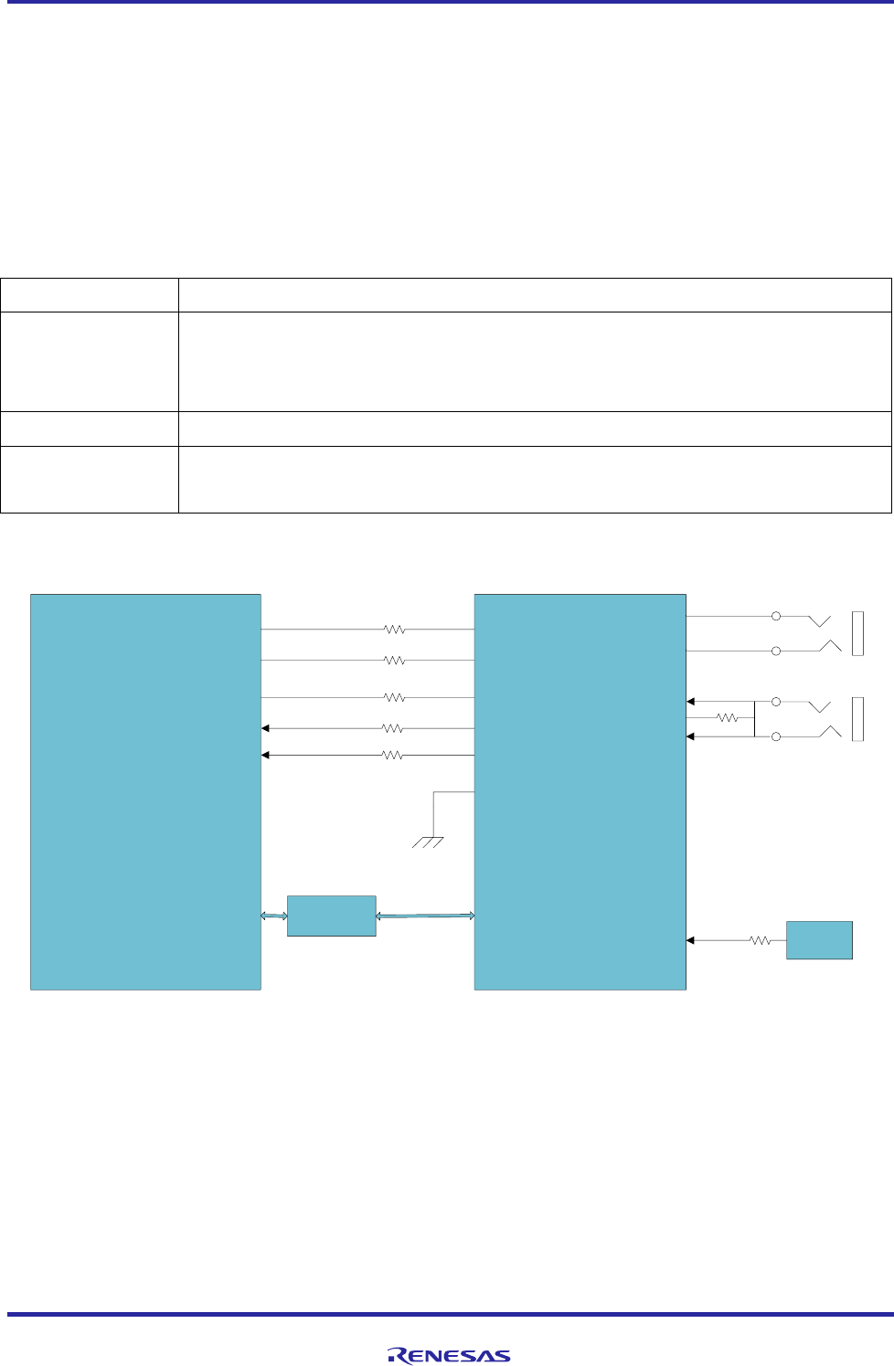
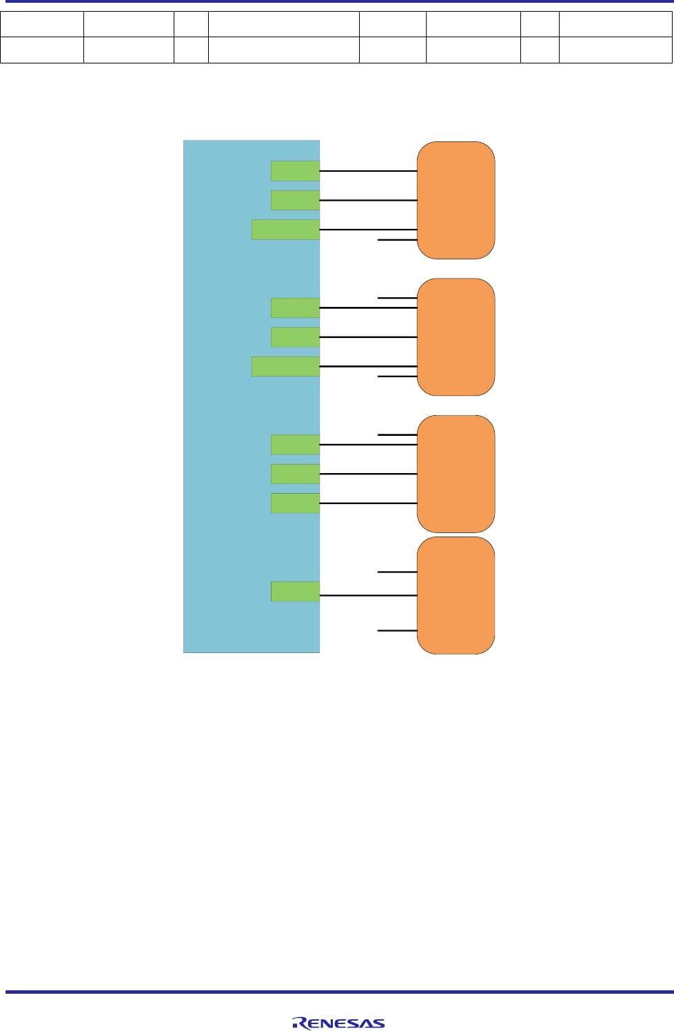
1 Overview
The Tethys board is R-Car W2H-specific evaluation board that can be used to evaluate systems using the R-Car
W2H and to develop operating systems, device drivers, and applications. Using the Tethys board allows developers to
efficiently conduct required tasks such as evaluating the performance of R-Car W2H-based systems, thus greatly
reducing turn-around times in product development.
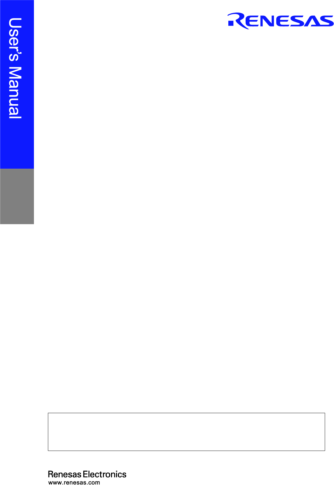
SD Card CN2
GPS Antenna CN7
HSM CN14
CAN&Flexray
CN6
Ethernet CN3
Audio jack
J1
USB CN1
DEBUG CN4
POWER Switch
SW18
POWER IN JACK
CN17 and CN18
Micro USB : CN16、CN10、CN5
ETNB CN13
D12 (GPS_LED)、D4、D6、D8、D10
CN9、CN8、CN12、CN11
SW1、SW2
SW11、SW10、SW9、SW8
SW16、SW15、SW14、SW13、SW4 (MCU reset)
D9、D7、D5、D3、D11 (GPS_LED)
SW5、SW6、SW7
Hardware Design Specification
ASD-B-16-0247 Rev1.3 Page
10
of 105
September 8, 2017
RTK00V2XRC7746SFS
1.1 Features
1.1.1 Features of the Tethys Board
Table 1 Features of the Tethys Board
Item
Description
CPU
·U1:R-Car W2H
( Operating clock: ARM 1.0GHz(Max), SH-4AL 260MHz)
MCU
·U32:RH850F1H/F1L
( Operating clock: RH850F1H 120MHz, RH850F1L 60MHz)
Audio Interfaces
·J1:
(1) L/R Audio output for SSI0
(2) Microphone input for SSI1
Connectors
·CN6:CAN & Flexray Connector( Flexray’s software not support)
·CN7:GPS ANT Connector
·CN14:HSM Connector(Software not support)
·CN13:ETNB Connector (Software not support)
PCIE Connectors
·CN9:Mini PCIE Connector for V2X Sub Board
·CN8: Mini PCIE Connector for Ethernet AVB Sub Board (Software not support)
·CN12:Mini PCIE Connector for V2X Sub Board
·CN11:Standard Mini PCIE
Debugger Interfaces
·CN4:26 pin FPC connector for CPU and MCU.
·CN10:UART-USB for Debug
·CN5:UART-USB for CPU Debug
·CN16:UART-USB for MCU Debug
Network Interfaces
·CN3:10M/100M Ethernet connector for Ethernet MAC
Storage Interfaces
·CN1:USB2.0 type A receptacle x 2
·CN2:SD card slots for SDHI2
·eMMC memory for MMC
Power Supply
·CN17 or CN18: DC 12V input
Hardware Design Specification
ASD-B-16-0247 Rev1.3 Page
11
of 105
September 8, 2017
RTK00V2XRC7746SFS
1.1.2 Functions of the Tethys Board
Table 2 List of Tethys Board Functions
Board Function
Tethys
RAM
DDR3 I/F: DDR3-SDRAM 1600MHz 1 GB x2
USB 2.0
USB2.0 CH0 : USB2.0 type A
USB2.0 CH1 : USB2.0 type A
SDHI
SDHI0 : Mini PCIE Connector for V2X Sub Board
SDHI2 : SD card slots , Mini PCIE Connector for V2X Sub Board
SCIF
SCIF0_D/HSCIF0_B : (1) Mini PCIE Connector for V2X Sub Board ,
(2) UART-USB
SCIF3_B/HSCIF2 : Mini PCIE Connector for V2X Sub Board
SCIF2_B(Debug serial) : UART-USB for CPU Debug
SCIF5_C : GPS Module
ROM(QSPI)
QSPI0 : SPI Flash 64MB
QSPI1 : SPI Flash 4MB
Ethernet MAC / Ethernet AVB
Ethernet MAC: RJ45 Connector
Ethernet AVB: Mini PCIE Connector for Ethernet AVB Sub Board (Ethernet AVB’s software
not support)
HSCIF
HSCIF1_A: Mini PCIE Connector for Ethernet AVB Sub Board (Ethernet AVB’s software
not support)
SCIF0_D/HSCIF0_B : (1) Mini PCIE Connector for V2X Sub Board ,
(2) UART-USB
SCIF3_B/HSCIF2 : Mini PCIE Connector for V2X Sub Board
I2C
I2C1_A/SPI : HSM Connector (Software not support)
I2C1_A : G-Sensor , Gyro , MCU
SSI
SSI0,1,2,9 : Audio CODEC
MSIOF
MSIOF1_B : MCU [Flexray (Software not support)、Ethernet AVB’s software not support]
MMC
MMC : eMMC(8GB)
PCI Express
Mini PCIE Connector
CAN
R-CAR W2H CAN channel support, RH850 CAN0/1 support, Flexray Software not support
Debug I/F
DBG : TO Sub Connector
VCC
Power Block
.

Hardware Design Specification
ASD-B-16-0247 Rev1.3 Page
12
of 105
September 8, 2017
RTK00V2XRC7746SFS
1.2 Usage Notes
1.2.1 Specifications of the Tethys Board
When the AC adapter is connected to the outlet, the 12V DC power is supplied to the Tethys board and some of the circuitry start
operating. Setting the ACC switch (SW18) to the ON side after that leads to the generation of various power supply levels including
5V DC and 3.3V DC from the 12V DC power.
Take particular care to ensure the correct configurations of the jumpers and switches mounted on the Tethys board. Incorrect
configurations may damage on-board devices.
For power supply to the Tethys, be sure to use the power supply that comes with it. Applying a voltage greater than 12 V may
damage devices on the Tethys board.
There are sequences for turning on and off the power supply to the Tethys board. Be sure to obey the notes below when using
the Tethys board.
(1) When turning on the power
Be sure to confirm that the ACC switch (SW18) is off before plugging the AC adapter into the power source.
It is prohibited to plug the AC adapter into a power source while the ACC switch (SW18) is on.
(2) When turning off the power
Be sure to turn off the ACC switch (SW18) before unplugging the AC adapter from the power source.
It is prohibited to unplug the AC adapter from the power source while the ACC switch (SW18) is on.
The AC adapter that comes with the Tethys board can supply current up to 3A at 12V. If you intend sub board to PCIe connect
on Tethys board, ensure that this does not lead to supply current exceeding 3A.
If the system configuration is such that the current supply does exceed 3A, prepare a separate stabilized DC power supply that
can supply more current at 12V.
Regarding the dedicated socket for the R-Car W2H, neither disconnect it from nor connect it to the Tethys board; also,
regarding the R-Car W2H, neither remove it from nor insert it in the dedicated socket. Both actions lead to malfunctions of
R-Car W2H operation on the board due to loosening of contacts between the socket and the board and between the socket and
the R-Car W2H.
Hardware Design Specification
ASD-B-16-0247 Rev1.3 Page
13
of 105
September 8, 2017
RTK00V2XRC7746SFS
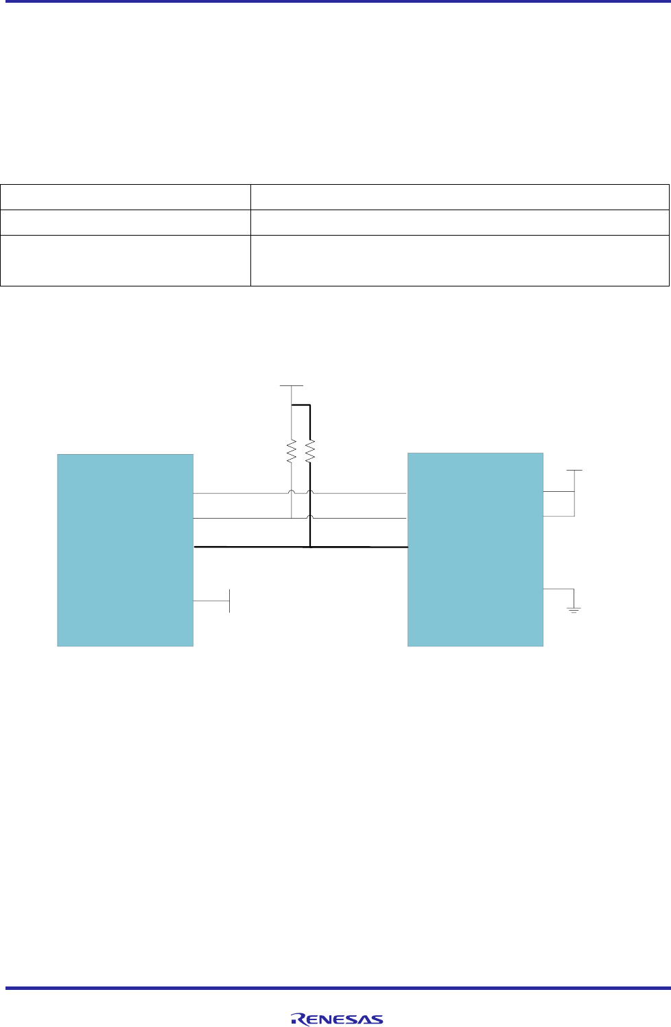
1.3 Board Configuration
The Tethys board is composed of a single board whose size is 185 mm ×110 mm
1.3.1 Block Diagram of the Tethys Board
Figure 1 shows a block diagram of the Tethys board
DDR3 I/F
DDR3 4G*32 bit
2 devices
DDR3 4Gbit
2 devices
MT41K256M16HA-125
Micron QSPI
RJ45 CN
HY911105AE
Hanrun
EtherMAC/
EtherAVB
USB 2.0-H
Type-A CN 2 in1
1775468-1
Samtec
USB 2.0 CH1
USB 2.0 CH0
HSCIF1_A
GPIO
SCIF0_D/HSCIF0_B
USB micro-B CN
47346-0001
Molex
Tact SW 4bit
SKRKAEE010
ALPS
Emmc(8GB)
SDIN8DE1-8G-XA
Sandisk
SDHI0
SDHI2
Mini PCI
Express CN
1759546-1
TE
USB to UART
CP2102
Silicon
SD Card Slot CN
503182-1852
Molex
MMC
GPIO Power Block
VCC
CAN CN
TSW-104-08-F-D
Samtec
GPIO
CAN0_C
1PPS
HSCIF2
DBG
USB to UART
CP2102
Silicon
SCIF2_B
(debug serial)
Tethy Board
1PPS
LED 4bit
SML-D13FW
ROHM
MCU
RH850F1H
Renesas
I2C1_A
RESET
To sub Connector
FH12-20S-0.5SV
Irios
GPS Module
NEO-7M
U-blox
GPS ANT
U.FL-R-SMT
Murata
CAN CN
TSW-104-08-F-D
Samtec
RMII PHY
KSZ8041RNLI
Micrel
SPI Flash(4MB)
S25FL132K0XMFI011
Spansion
SPI Flash(64MB)
S25FL512SAGMFIG11
Spansion
GPIO
GPIO
CPU
R-CarW2H
Renesas
BU12V
CAN transceiver
TJA1050
NXP
CAN
transceiver
TJA1050
NXP
Mini PCI
Express CN
1759546-1
TE
Mini PCI
Express CN
1759546-1
TE
USB micro-B CN
47346-0001
Molex
USB to UART
CP2102
Silicon
USB micro-B CN
47346-0001
Molex
GPIO
SCIF3_B/HSCIF2
CAN CN
TSW-104-08-F-D
Samtec
CAN
transceiver
TJA1050
NXP
1PPS
G-Sensor
AIS328DQ
ST
Gyro
A3G4250D
ST
I2C1_A
USB2.0 CH1-2
USB 2.0 CH1-4
USB 2.0 CH1-3 SCIF5_C
USB HUB
GL852GT-MNGXX
GENESYS
USB 2.0 CH1-2,3,4
USB CH1 -1
CPU JTAG CN
HTST-110-01-S-DV
Samtec
MCU JTAG CN
1-1634688-4
Samtec
Connector
FH12-20S-0.5SV
Irios
Debug Board
GPIO
FPC
MSIOF1_B
PCI Express
Mini PCI
Express CN
1759546-1
TE
I2C1_A/SPI
Mini Jack Line OUT Audio DAC/ADC
AK4642
AKM SSI0,1,2,9
HSM CN
FlexrayDriver FlexrayCN
EtherAVB CN
CPU SH4A JTAG CN
1-1634688-4
Samtec
Figure 1 Block Diagram of the Tethys Board
Notice:
White text means not support the function
(HSM CN, Flexray_CN, Ethernet AVB CN)
Hardware Design Specification
ASD-B-16-0247 Rev1.3 Page
14
of 105
September 8, 2017
RTK00V2XRC7746SFS
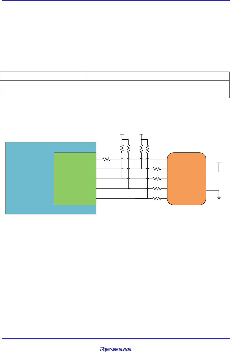
2 Operating condition and antenna characteristic
2.1 Operating condition
Table 3 shows the operating condition. To use the Tethys board system, please keep the condition.
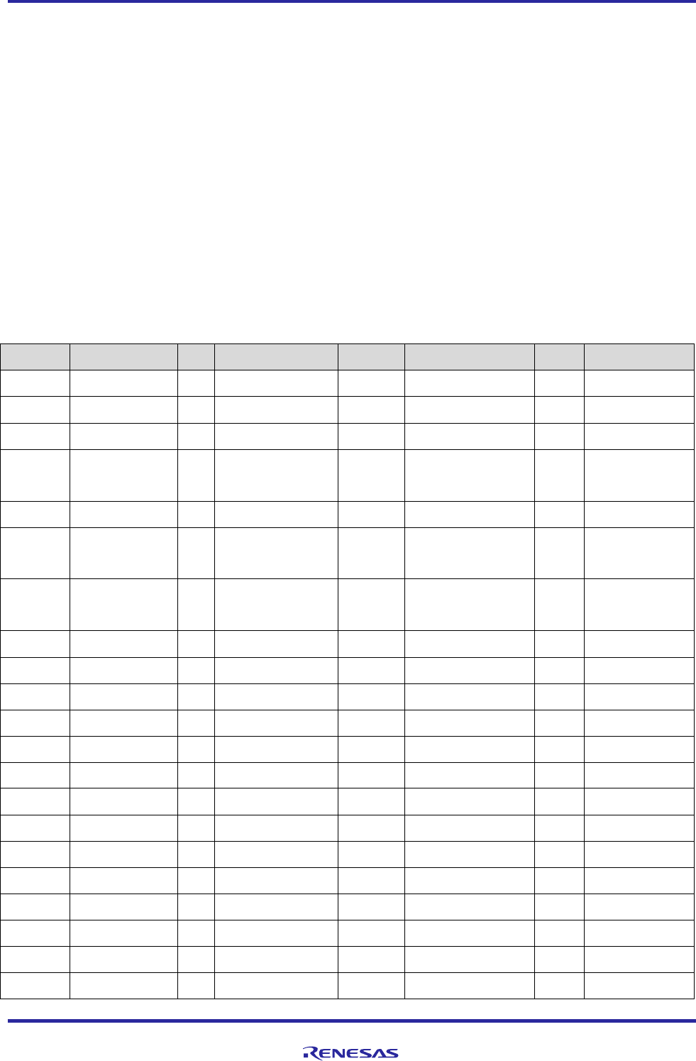
Table 3 Operating Condition
Item
Min
Typ
Max
Units
Input Voltage
7
12
25
V
Consumption Current
200
450
3000(*1)
mA
Operating Temperature
-25
25
+85
Degree C
V2X antenna Frequency range
5860
5920
MHz
V2X antenna VSWR
2.0
V2X antenna Gain
2M Cable Type:
(1)3.0(without cable loss)
(2) -1.0(with cable loss)
Rod Type:
(1)5.0
dBi
V2X antenna Cable Loss
4.0 (L=2m)
dB
GPS antenna Center Frequency
1575 ± 3
MHz
GPS antenna VSWR
2.0
GPS antenna Bandwidth
20
MHz
GPS antenna Gain
30
dB
Storage Temperature
-25
85
Degree C
Operating Humidity
25
85(*2)
%
Notice:
(*1): 3000mA is the maximum current of AC adapter. If user need more current for Tethys board, user need
prepare stable big current AC adapter.
(*2): Humidity: No condensation.
Hardware Design Specification
ASD-B-16-0247 Rev1.3 Page
15
of 105
September 8, 2017
RTK00V2XRC7746SFS
3 Specifications of Interface Modules on the Tethys Board
This section describes the main function of the Tethys board, which includes the following sections:
3.1 Mode Setting
3.1.1 Specifications
The operating mode of the R-Car W2HR-Car W2H is set by a power-on reset. For details on the operating mode, see the
documents related to the R-Car W2HR-Car W2H operating mode specifications.
3.1.2 MD0 Pin -Selection of Free-Running Mode or Step-Up Mode
Do not change the initial setting at shipment (MD0=0).
3.1.3 MD [3:1] Pins-Selection of Boot Device
These pins select the boot device.
MD3
MD2
MD1
Selection of Boot Device
0
0
0
External ROM boot (area 0)
0
0
1
eMMC boot via SDHI1
0
1
0
Serial flash ROM boot via QSPI; 16Kbytes transferred at 48.75 MHz
0
1
1
Reserved
1
0
0
Serial flash ROM boot via QSPI; 16Kbytes transferred at 39 MHz
1
0
1
Reserved
1
1
0
Serial flash ROM boot via QSPI; 4 Kbytes transferred at 39 MHz
1
1
1
Reserved
3.1.4 MD4 Pin-Selection of CS0 Space Size
This pin selects whether the area 0 space (CS0) is used as a normal space (64 Mbytes) or an expanded space (128 Mbytes).
MD4
Area Division
0
Area 0: 64 Mbytes
1
Area 0: 128 Mbytes
3.1.5 MD5 Pin-Reserved
Do not change the initial setting at shipment (MD5=1).
3.1.6 MD [7:6] Pins-Selection of Master Boot Processor
These pins select the master boot processor.
Hardware Design Specification
ASD-B-16-0247 Rev1.3 Page
16
of 105
September 8, 2017
RTK00V2XRC7746SFS
MD7
MD6
Selection of Master Boot Processor
0
0
Setting prohibited
0
1
Booted through CPU0 in CA7.
1
0
Booted through SH-4AL in 32-bit mode
1
1
Setting prohibited
3.1.7 MD8 Pin-Selection of Area 0 Space Data Bus Width
This pin sets the data bus width of the area 0 space (CS0) to 8 bits or 16 bits. Select the data bus width of the boot device
connected to the LBSC.
MD8
EXBUS Area 0 Data Bus Width
0
8-bit bus
1
16-bit bus
3.1.8 MD9 Pin-Selection of Crystal Resonator or Crystal Oscillator
This pin selects either a crystal resonator or a crystal oscillator to be connected to the EXTAL/XTAL pins. A crystal oscillator
(Y2: 20 MHz) is mounted on the Tethys board by default.
MD9
EXTAL/XTAL Pin Setting
0
An external clock is input to the EXTAL pin.
1
A crystal resonator is connected to the EXTAL and XTAL pins.
3.1.9 MD21, MD20, MD11, MD10, and MDT [1:0] Pins-Switching of JTAG, SDHI1, and SDHI2
These pins select the debugging function through the JTAG connector (CN4) or the SD card slot for the SDHI1. The debugging
through the SDHI1 or SDHI2 is possible by the combination of MD pin settings in the R-Car W2H specifications.
MD10
MD[21:20]
MD11
MDT[1:0]
JTAG
MMC
SDHI2
0
00
-
--
Boundary scan
Normal function
Normal function
0
01
-
--
Reserved
Reserved
Reserved
0
10
0
--
Coresight (*1)
Normal function
Normal function
0
10
1
00
Coresight (*1)
Reserved
Reserved
0
10
1
01
Coresight (*1)
SH-4AL
Normal function
0
10
1
10
Coresight (*1)
Reserved
Reserved
0
10
1
11
Coresight (*1)
Normal function
SH-4AL
0
11
0
--
SH-4AL
Normal function
Normal function
0
11
1
00
SH-4AL
Coresight (*1)
Normal function
1
00
-
--
Reserved
Reserved
Reserved
1
01
0
--
Reserved
Reserved
Reserved
1
01
1
01
Reserved
Reserved
Reserved
1
10
-
--
Reserved
Reserved
Reserved
1
11
-
--
Reserved
Reserved
Reserved
Hardware Design Specification
ASD-B-16-0247 Rev1.3 Page
17
of 105
September 8, 2017
RTK00V2XRC7746SFS
(*1) “Coresight” is an abbreviation of “Coresight debug port”.
3.1.10 MD [14:13] Pins-Frequency Mode Setting
These pins select the frequency mode. A crystal oscillator (Y2: 20 MHz) is mounted on the Tethys board. Do not change the
initial setting at shipment (MD14 = 0, MD13 = 0).
MD14
MD13
EXTAL
Frequency
EXTAL
Divider
PLL0 Multiplication
Ratio
PLL1 Multiplication
Ratio
PLL3 Multiplication Ratio
0
0
20 MHz
× 1
×80
VCO = 1600 MHz
×78
VCO = 1560 MHz
×50
VCO = 1000 MHz
0
1
26 MHz
× 1
×60
VCO = 1560 MHz
×60
VCO = 1560 MHz
×56
VCO = 1456 MHz
1
0
Prohibited
setting
1
1
30 MHz
× 1
×52
VCO = 1560 MHz
×52
VCO = 1560 MHz
×50
VCO = 1500 MHz
3.1.11 Initial Values of Mode Setting Pins on Tethys Board
The following table shows the Initial Values of Mode Setting Pins on the Board, and how the individual mode pins are set:
MD Pins
Initial
Value
Initial Function
Setting Method
MD0
0
-
Set by a dip switch
MD[3:1]
010
Boot from the QSPI(48.75 MHz/16-Kbyte
transfer)
Set by a dip switch
MD4
0
CS0 space size (64 Mbytes)
Set by a dip switch
MD5
1
-
Set by a dip switch
MD[7:6]
01
Cortex-A7 boot
Set by a dip switch
MD8
1
CS0 space data bus width (16 bits)
Set by a dip switch
MD9
1
Crystal resonator is used.
Set by a dip switch
MD10, MD[21:20], MD11,
MDT[1:0]
0,10,0,00
JTAG = Coresight
SDHI1 and SDHI2 = Normal function
Set by a dip switch
MD[14:13]
00
Input frequency = 20 MHz
Set by a dip switch
3.2 DDR3-SDRAM Interface (DBSC)
3.2.1 Specifications
The Tethys board incorporates two 4-Gbit DDR3-SDRAMs (16-bit bus width) and operates at a maximum speed of
Hardware Design Specification
ASD-B-16-0247 Rev1.3 Page
18
of 105
September 8, 2017
RTK00V2XRC7746SFS
DDR3-1000. The Tethys board can support memory size up to 2GB (8-Gbit memory x 2) and the data bus width is 32 bits x1. The
DDR3-SDRAMs are allocated to the address space from H'01_0000 0000 to H'01_FFFF FFFF in the R-Car W2H. The address
ranges from H'00_40000000 to H'00_BFFF FFFF can be accessed by default as a mirror area of H'01_0000 0000 to H'01_7FFF
FFFF.
Table 4 DDR3-SDRAM Interface Specifications
Controller
On-chip external bus controller for DDR3-SDRAM (DBSC) in the R-Car W2H
Product name
MT41K256M16HA-125 AAT:E from Micron
DDR3-1600 (x 16 bits, 4 Gbits) x 2 pcs
Power supply voltage
1.50 V
Capacity
H'01_0000 0000 to H'01_FFFF FFFF
Bus width
32-bit data bus
Memory bus frequency(R-Car W2H Spec.)
DDR3-1000
3.2.2 Signal Connections between R-Car W2H and DDR3-SDRAMs
Table 5 Signal Connections between R-Car W2H and DDR3-SDRAMs
R-Car W2H
DDR3-SDRAM (U3)
DDR3-SDRAM (U4)
D[31:16]
D[15:0]
M0DQ[31:16]
DQ[15:0]
--
M0DQ[15:0]
--
DQ[15:0]
M0A[15:0]
A[15:0]
←
M0BA[2:0]
BA[2:0]
←
M0CK1、M0CK1#
CK、CK#
--
M0CK0、M0CK0#
--
CK、CK#
MCKE1
CKE
--
MCKE0
--
CKE
M0CS1#
CS#
--
M0CS0#
--
CS#
M0WE#
WE#
←
M0RAS#
RAS#A
←
M0CAS#
CAS#
←
M0DQS3、M0DQS3#
UDQS、UDQS#
--
M0DQS2、M0DQS2#
LDQS、LDQS#
--
M0DQS1、M0DQS1#
--
UDQS、UDQS#
M0DQS0、M0DQS0#
--
LDQS、LDQS#
M0DM3、M0DM2
UDM、LDM
--
M0DM1、M0DM0
--
UDM、LDM
Hardware Design Specification
ASD-B-16-0247 Rev1.3 Page
19
of 105
September 8, 2017
RTK00V2XRC7746SFS
M0ODT1
ODT
--
M0ODT0
--
ODT
M0RESET#
RESET#
←
3.2.3 Block Diagram
R-CarW2H
M0DQ[31:0]
M0A[15:0]
M0BA[2:0]
M0RAS#
M0CAS#
M0WE#
M0RESET#
M0CS0#
M0CKE0
M0ODT0
M0CK0
M0CK0#
M0DQS[1:0]
M0DQS[1:0]#
M0DM[1:0]
M0CKE1
M0ODT1
M0CK1
M0CK1#
M0DQS[3:2]
M0DQS[3:2]#
M0DM[3:2]
M0BKPRST#
M0VREFDQ1
M0VREFDQ0
M0VREFCA
M0ZQ
A[15:0]
BA[2:0]
RAS#
CAS#
WE#
RESET#
CS#
CKE
ODT
CK
CK#
DQS
DQS#
DM
DQS
DQS#
DM
DQL[7:0]
DQU[7:0]
VREFCA
VREFDQ
DQL[7:0]
DQU[7:0]
0.1uF 0.1uF
0.1uF
20K20K
DDR3
0.1uF 0.1uF
0.1uF
20K20K
M0BKPRST D1.5V D1.5V
120
MT41K256M16H
A-125 AAT:E
0.1uF 0.1uF
20K20K
22
22
22
22
22
M0CS1# CS#
22
22
CKE
22
22
22
100
M0ZQ
240
ODT
CK
CK#
D1.5V
0.1uF
51
51
0
0.1uF
Figure 2 Block Diagram of the DDR3-SDRAM Interface
Hardware Design Specification
ASD-B-16-0247 Rev1.3 Page
20
of 105
September 8, 2017
RTK00V2XRC7746SFS
3.3 SPI-Flash Interface (QSPI)
3.3.1 Specifications
The Tethys board incorporates 512-Mbit and 32-Mbit SPI flash memory devices manufactured by Spansion. These flash memory
devices are connected to the QSPI of the R-Car W2H’s pin of (GP1_21/QSPI0_SSL/WE1#). And the connection is controlled by
SW9 When the 512-Mbit SPI flash memory is to be assessed, set SW9 pin 3 and 6 short, and when the 32-Mbit SPI flash memory is
to be accessed, set SW9 pin 4 and 8 short. Do not short them at the same time.
Table 6 SPI-Flash Interface Specifications
Flash memory interfaces
QSPI0 and QSPI1 in the R-Car W2H
Operating voltage
D3.3 V_FLASH = 3.3V
Capacity
512-Mbit and 32-Mbit
Mapping area (512-Mbit)
0x0000000~0x3ffffff
Mapping area (32-Mbit)
0x0000000~0x3fffff
3.3.2 Block Diagram
R-Car W2H
SPI FLASH
S25FL132K0XMFI011
32Mbit
U6
GP1_21/QSPI0_SSL/WE1#
GP1_20/QSPI0_IO3/RD#
GP1_19/QSPI0_IO2/CS0#
GP1_18/QSPI0_MISO/QSPI0_IO1/RD/WR#
GP1_17/QSPI0_MOSI/QSPI0_IO0/BS#
GP1_16/QSPI0_SPCLK/WE0#
CS#
QSPI_IO3
QSPI_IO2
QSPI_SO/IO1
QSPI_SI/IO0
QSPI_CLK
HOLD#/IO3
W#/ACC/IO2
SI/IO0
SI/IO1
CLK
QSPI
D3.3V_FLASH
SPI FLASH
S25FL512SAGMFIG11
512Mbit
U5
CS#
DQ3
DQ2
DQ0
DQ1
CLK
D3.3V_FLASH
5
6
4
3
SW9
Figure 3 Block Diagram of the SPI-Flash Interface
QSPI0 devices
U5:S25FL512SAGMFIG11 (512 Mbits, 8-/16-bit data width) from Spansion ×1 pcs
U6:S25FL132K0XMFI011(32Mbits, 8-/16-bit data width) from Spansion ×1 pcs
Hardware Design Specification
ASD-B-16-0247 Rev1.3 Page
21
of 105
September 8, 2017
RTK00V2XRC7746SFS
3.4 Audio Codec Interfaces (SSI0, SSI1)
3.4.1 Specifications
The Tethys board incorporates an audio codec (AK4642EN, U29) which is connected to SSI0 and SSI1 of the R-Car W2H. For
details on the SSI, see the R-Car W2H Hardware Manual. For details on the AK4642EN, see the datasheet published by Asahi Kasei
Micro devices.
Table 7 SSI Codec Specifications
Controller
On-chip SSI0and SSI1 in the R-Car W2H
Audio codec
AK4642EN (U29) from AKM
I2C bus : Interface 1
I2C slave address: 0x25 for read, 0x24 for write (CAD0= 0)
Master/slave mode
AK4642EN: Master/slave selectable(slave mode by default)
Audio connector
MIC IN (J1)
LINE-OUT( J1)
3.4.2 Block Diagram
U1
R-Car W2H
GP5_9/SSI_SCK0129_A
GP5_10/SSI_WS0129_A
U29
AUDIO
AK4642EN
GP5_11/SSI_SDATA0_A
LRCK
BICK
SDTI
0
0
0
GP5_21/SSI_SDATA1_A
0
SDTO
GP5_28/AUDIO_CLKA_A 22 MCKO
I2C Buffer
LTC4313IMS8-
1#PBF
CSN/CAD0
MCK
IX3
12.288MHz
LOUT
ROUT
RIN1/IN1+
LIN1/IN1-
MPWR 2K 1%
J1
Line Out
J1
MIC In
Figure 4 Block Diagram of the Audio Codec Interface
Hardware Design Specification
ASD-B-16-0247 Rev1.3 Page
22
of 105
September 8, 2017
RTK00V2XRC7746SFS
3.5 eMMC Memory Interface (eMMC)
3.5.1 Specifications
The Tethys board incorporates an eMMC memory SDIN8DE1-8G-XA manufactured by SanDisk that is connected to the on-chip
MMC interface of the R-Car W2H.For details on the MMC, see the R-Car W2H Hardware Manual.
Table 8 eMMC Memory Interface (eMMC) Specifications
MMC controller
On-chip MMC in the R-Car W2H
Interface voltage control
D3.3V_eMMC=3.3V
eMMC memory
SDIN8DE1-8G-XA(U7) from SanDisk
Capacity:8GB
3.5.2 Block Diagram
MMC_CLK
MMC_CMD
MMC_D[7:0]
VCCQ_MMC
eMMC
CLK
CMD
DATA[7:0]
D3.3V
VCCQ
VCC
D3.3V_eMMC
10K
D3.3V_eMMC
R-Car W2H
Figure 5 Block Diagram of the eMMC Memory Interface
Hardware Design Specification
ASD-B-16-0247 Rev1.3 Page
23
of 105
September 8, 2017
RTK00V2XRC7746SFS
3.6 SD Card Host Interface (SDHI2)
3.6.1 Specifications
The Tethys board incorporates a SD card slot (CN2) and a mini-PCI Express CN (CN12) for the on-chip SD card host interface
(SDHI2) of the R-Car W2H. For details on the SDHI2, please refer to the R-Car W2H hardware manual. CN12 and CN2 can not be
used at the same time.
Table 9 Specifications of SD Card Host Interface (SDHI2)
SD Host Interface
On-chip SDHI2 in the R-Car W2H
Voltage control for VDD
VCCQ_SD2 =3.3V/1.8V it can be switched by software , D3.3V=3.3V
SD Card Slot
503182-1852(CN2) from Molex
3.6.2 Block Diagram
R-Car W2H SDHI2
SD2_CLK
SD2_DATA[3:0]
SD2_CD
SD2_WP
SD2_CMD
VCCQ_SD2
47K
100
33
33
33
33
CLK
DATA[3:0]
WP
CD
CMD
SD Slot
CN2
D3.3V
D3.3V
Figure 6 Block Diagram of the SDHI2 Interface
Hardware Design Specification
ASD-B-16-0247 Rev1.3 Page
24
of 105
September 8, 2017
RTK00V2XRC7746SFS
3.7 Mini PCI Express Interface
3.7.1 Specifications
The Tethys board incorporates four mini PCIE interface manufactured by TE. One Mini-PCI Express CN(CN9) is connected to
SDHI0, GPIO, SCIF0 and the HSCIF0 of the R-Car W2H, another Mini-PCI Express CN(CN12) is connected to SDHI2, GPIO,
SCIF3 and the HSCIF2 of the R-Car W2H, and the third Mini-PCI Express CN(CN8) is connected to the Ethernet MAC/Ethernet
AVB, GPIO and the HSCIF1 of the R-Car W2H, The fourth Mini-PCI Express CN(CN11) acts as a standard Mini-PCI Express
signal connector and transmits the standard Mini-PCI Express signals. There are also USB 2.0 signals and 1pps signal connected to
the mini PCIE connectors.
3.7.2 The Mini PCIE connector signal configuration are shown as below:
3.7.2.1 CN9 of figure 7 signal assignments are shown as below:
Pin NO.
Signal
I/O
Remark
Pin NO.
Signal
I/O
Remark
1
C2X0_DCMODE
O
GPIO
2
D3.3V
PO
Power
3
N.C.
-
4
GND
-
Power
5
PCIE_5.0V
PO
Power
6
PCIE_5.0V
PO
Power
7
C2X0_RESETB
O
GPIO
8
GPS_1PPS/
C2X0_GPIO_B3
I/O
GPS 1PPS output
or GPIO
9
GND
-
Power
10
C2X0_GPIO_B2
I/O
GPIO
11
RX0_D/
C2X_RXD
I
UART from CPU
or USB2UART
12
C2X0_GPIO_B1
I/O
GPIO
13
TX0_D/
C2X_TXD
O
UART from CPU
or USB2UART
14
C2X0_GPIO_B0
I/O
GPIO
15
GND
-
Power
16
C2X0_STATE
I
C2X state
17
N.C.
-
18
GND
-
Power
19
N.C.
-
20
C2X0_GPIO_A6
I/O
GPIO
21
GND
-
Power
22
C2X0_GPIO_A5
I/O
GPIO
23
HRX0_B
I
UART from CPU
24
PCIE_5.0V
PO
Power
25
HTX0_B
O
UART from CPU
26
GND
-
Power
27
GND
-
Power
28
PCIE_5.0V
PO
Power
29
GND
-
Power
30
C2X0_GPIO_A4
I/O
GPIO
31
MD10/HCTS0#
I/O
UART from CPU
32
C2X0_GPIO_A3
I/O
GPIO
33
MD11/HRTS0#
I/O
UART from CPU
34
GND
-
Power
35
GND
-
Power
36
N.C
-
37
SD0_CLK
O
SD0 clock
38
N.C
-
39
SD0_WP
I
SD0 write protect
40
GND
-
Power
41
SD0_CD
I
SD0 card detect
42
C2X0_GPIO_A2
I/O
GPIO
Hardware Design Specification
ASD-B-16-0247 Rev1.3 Page
25
of 105
September 8, 2017
RTK00V2XRC7746SFS
43
SD0_DATA3
I/O
SD0 data3
44
C2X0_GPIO_A1
I/O
GPIO
45
SD0_DATA2
I/O
SD0 data2
46
C2X0_GPIO_A0
I/O
GPIO
47
SD0_DATA1
I/O
SD0 data1
48
PCIE_5.0V
PO
Power
49
SD0_DATA0
I/O
SD0 data0
50
GND
-
Power
51
SD0_CMD
I/O
SD0 command
52
D3.3V
PO
Power
3.7.2.2 CN12 of figure 7 signal assignments are shown as below:
Pin NO.
Signal
I/O
Remark
Pin
NO.
Signal
I/O
Remark
1
C2X1_DCMODE
O
GPIO
2
D3.3V
PO
Power
3
N.C.
-
4
GND
-
Power
5
PCIE_5.0V
PO
Power
6
PCIE_5.0V
PO
Power
7
C2X1_RESETB
O
GPIO
8
GPS_1PPS/
C2X1_GPIO_B3
I/O
GPS 1PPS output
or GPIO
9
GND
-
Power
10
C2X1_GPIO_B2
I/O
GPIO
11
RX3_B
I
UART from CPU
12
C2X1_GPIO_B1
I/O
GPIO
13
TX3_B
O
UART from CPU
14
C2X1_GPIO_B0
I/O
GPIO
15
GND
-
Power
16
C2X1_STATE
I
C2X state
17
N.C.
-
18
GND
-
Power
19
N.C.
-
20
C2X1_GPIO_A6
I/O
GPIO
21
GND
-
Power
22
C2X1_GPIO_A5
I/O
GPIO
23
HRX2
I
UART from CPU
24
PCIE_5.0V
PO
Power
25
HTX2
O
UART from CPU
26
GND
-
Power
27
GND
-
Power
28
PCIE_5.0V
PO
Power
29
GND
-
Power
30
C2X1_GPIO_A4
I/O
GPIO
31
HCTS2#
I/O
UART from CPU
32
C2X1_GPIO_A3
I/O
GPIO
33
HRTS2#
I/O
UART from CPU
34
GND
-
Power
35
GND
-
Power
36
USB1_DM3
I/O
USB data
negative
37
SD2_CLK
O
SD0 clock
38
USB1_DP3
I/O
USB data
positive
39
SD2_WP
I
SD0 write protect
40
GND
-
Power
41
SD2_CD
I
SD0 card detect
42
C2X1_GPIO_A2
I/O
GPIO
43
SD2_DATA3
I/O
SD0 data3
44
C2X1_GPIO_A1
I/O
GPIO
45
SD2_DATA2
I/O
SD0 data2
46
C2X1_GPIO_A0
I/O
GPIO
47
SD2_DATA1
I/O
SD0 data1
48
PCIE_5.0V
PO
Power
49
SD2_DATA0
I/O
SD0 data0
50
GND
-
Power
51
SD2_CMD
I/O
SD0 command
52
D3.3V
PO
Power
Hardware Design Specification
ASD-B-16-0247 Rev1.3 Page
26
of 105
September 8, 2017
RTK00V2XRC7746SFS
3.7.2.3 CN8 of Figure 7 signal assignments are shown as below:
Pin NO.
Signal
I/O
Remark
Pin NO.
Signal
I/O
Remark
1
AVB_TX_ER
O
Transmit error signal
2
D3.3V
PO
Power
3
AVB_MDIO
I/O
Management information
transmit/receive data
4
GND
-
Power
5
PCIE_5.0V
PO
Power
6
PCIE_5.0V
PO
Power
7
AVB_GPIO6
(AVB_CRS)
I
Carrier detection signal
8
ETH_CRS_DV/
AVB_RX_DV
I
Receive data
enable signal
9
GND
-
Power
10
ETH_RX_ER/
AVB_RXD3
I
Receive data
signal
11
AVB_PHY_INT
I
PHY interrupt signal
12
ETH_TXD0/
AVB_RX_ER
I
Reception error
signal
13
AVB_MDC
O
Management information
transfer clock signal
14
ETH_RXD1/
AVB_RXD1
I
Receive data
signal
15
GND
-
Power
16
ETH_MDIO/
AVB_RXD2
I
Receive data
signal
17
AVB_TX_CLK
I
Transmit clock signal
18
GND
-
Power
19
C2X1_RESETB/
AVB_GTX_CLK
O
GMII transmit clock signal
20
ETH_REF_CLK/
AVB_RX_CLK
I
Receive clock
signal
21
GND
-
Power
22
AVB_RESETn
O
GPIO
23
HRX1_A
I
High speed uart
24
PCIE_5.0V
PO
Power
25
HTX1_A
O
High speed uart
26
GND
-
Power
27
C2X1_GPIO_A1/
AVB_TXD7
O
Transmit data signal
28
PCIE_5.0V
PO
Power
29
C2X1_GPIO_B0/
AVB_TXD6
O
Transmit data signal
30
GTXREFCLK
O
GMII reference
clock signal
31
HCTS1#_A
I/O
High speed uart
32
ETH_RXD0/
AVB_RXD0
I
Receive data
signal
33
HRTS1#_A
I/O
High speed uart
34
GND
-
Power
35
C2X1_GPIO_B1/
AVB_TXD5
O
Receive data signal
36
USB1_DM2
I/O
USB data
negative
37
AVB_TXD3
O
Transmit data signal
38
USB1_DP2
I/O
USB data
positive
39
AVB_TXD0
O
Transmit data signal
40
GND
-
Power
41
AVB_TXD1
O
Transmit data signal
42
AVB_GPIO5
(AVB_RXD7)
I
GPIO
43
AVB_TXD2
O
Transmit data signal
44
ETH_TX_EN/
AVB_GPIO3
I
GPIO
Hardware Design Specification
ASD-B-16-0247 Rev1.3 Page
27
of 105
September 8, 2017
RTK00V2XRC7746SFS
(AVB_RXD6)
45
C2X1_GPIO_B2/
AVB_TXD4
O
Transmit data signal
46
AVB_GPIO4
(AVB_COL)
I
GPIO
47
ETH_LINK/
AVB_GPIO1
(AVB_RXD4)
I
GPIO
48
PCIE_5.0V
PO
Power
49
ETH_TXD1/
AVB_GPIO2
(AVB_RXD5)
I
GPIO
50
GND
-
Power
51
AVB_TX_EN
O
Transmit data enable
signal
52
D3.3V
PO
Power
3.7.2.4 CN11 of figure 7 signal assignments are shown as below:
Pin NO.
Signal
I/O
Remark
Pin NO.
Signal
I/O
Remark
1
N.C
-
2
D3.3V
PO
Power
3
N.C
-
4
GND
-
Power
5
N.C
-
6
D1.5V
PO
Power
7
N.C
-
8
N.C
-
9
GND
-
Power
10
N.C
-
11
PCIe_CLKN
I
PCIe clock minus
12
N.C
-
13
PCIe_CLKP
I
PCIe clock plus
14
N.C
-
15
GND
-
Power
16
N.C
-
17
N.C
-
18
GND
-
Power
19
N.C
-
20
N.C
-
21
GND
-
Power
22
N.C
-
23
PCIe_RXN
I
PCIe receive data minus
24
D3.3V
PO
Power
25
PCIe_RXP
I
PCIe receive data plus
26
GND
-
Power
27
GND
-
Power
28
D1.5V
PO
Power
29
GND
-
Power
30
I2C1-SCL
I/O
I2C clock
31
PCIe_TXN
O
PCIe transmit data minus
32
I2C1-SDA
I/O
I2C data
33
PCIe_TXP
O
PCIe transmit data plus
34
GND
-
Power
35
GND
-
Power
36
USB1_DM4
I/O
USB data negative
37
N.C
-
38
USB1_DP4
I/O
USB data positive
39
N.C
-
40
GND
-
Power
41
N.C
-
42
N.C
-
43
N.C
-
44
N.C
-
45
N.C
-
46
N.C
-
47
N.C
-
48
D1.5V
PO
Power
Hardware Design Specification
ASD-B-16-0247 Rev1.3 Page
28
of 105
September 8, 2017
RTK00V2XRC7746SFS
49
N.C
-
50
GND
-
Power
51
N.C
-
52
D3.3V
PO
Power
3.7.3 Block Diagram
R-car W2H
SDHI0
Mini PCI
Express CN
TE
CN9
GPIO
SCIF0/HSCIF0
SDHI2
Mini PCI
Express CN
TE
CN12
GPIO
Mini PCI
Express CN
TE
CN8
1PPS
USB 2.0
1PPS
SCIF3/HSCIF2
EtherAVB
GPIO
USB 2.0
HSCIF1
Mini PCI
Express CN
TE
CN11
PCIe
USB 2.0
I2C
Figure 7 Block Diagram of Mini PCI Express Interface
Hardware Design Specification
ASD-B-16-0247 Rev1.3 Page
29
of 105
September 8, 2017
RTK00V2XRC7746SFS
3.8 USB to UART
3.8.1 Specifications
The Tethys board incorporates three USB to UART bridges: One is connected to a mini PCIE connector, one is connected to
the R-Car W2H and another is connected to the MCU. Users can control and debug the Tethys board through the USB port.
Table 10 USB to UART Specifications
USB to UART IC
CP2102-GM from Silicon
USB function connector
47346-0001 from Molex x 3pcs
Common mode filter with ESD protection diode
PRTR5V0U2X from NXP x 3pcs
3.8.2 Block Diagram
R-car W2H
MCU
USB to UART
CP2102
Silicon
USB micro-B CN
CN10
USB to UART
CP2102
Silicon
USB micro-B CN
CN5
SCIF2
(debug)
USB to UART
CP2102
Silicon
USB micro-B CN
CN16
Mini PCI
Express CN
TE
ESD protection
PRTR5V0U2X
D22
ESD protection
PRTR5V0U2X
D24
ESD protection
PRTR5V0U2X
D23
Figure 8 Block Diagram of the USB to UART
USB controller
On-chip SCIF2(debug) function controller in the R-Car W2H, MCU,
and Mini PCI express CN
Hardware Design Specification
ASD-B-16-0247 Rev1.3 Page
30
of 105
September 8, 2017
RTK00V2XRC7746SFS
3.9 USB2.0 Interface
3.9.1 Specifications
The Tethys board incorporates two A Type USB Connectors for the USB2.0 host interface. The USB0 of the R-Car W2H is
connected to a USB 2.0 type A port directly. The USB1 of the R-Car W2H is connected to the GL852GT which manufactured by
Genesys to expand 4 USB 2.0. The expand 1 port of the GL852GT is connected to a USB 2.0 type A port. There is a switch IC for
the two USB ports’ power supply. The other 3 USB port of the GL650USB are connected to the three of four mini PCIE connectors
separately.
Table 11 USB2.0 Interface
USB controller
On-chip USB2.0 function controller in the R-Car W2H
USB Power Switch
BD2066FJ-LBE2 from ROHM
USB Hub
GL852GT-MNGXX from Genesys
USB host connector x 2
On-chip USB2.0 interface1 in the R-Car W2H
1759546-1 from TE x 2
Common mode filter with ESD protection diode
PRTR5V0U2X from NXP
Hardware Design Specification
ASD-B-16-0247 Rev1.3 Page
31
of 105
September 8, 2017
RTK00V2XRC7746SFS
3.9.2 Block Diagram
VBUS
GND
D+
D-
VBUS
GND
D+
D-
ESD Protection
PRTR5V0U2X
D2
USB0_DP
USB0_DM
USB1_DP
USB1_DM
CTRLA
FLAGA
CTRLB
FLAGB
1K
D3.3V
USB1_PWEN
USB1_OVC
USB0_PWEN
USB0_OVC
10K
USB 2.0
BD2066FJ
-LBE2
0
0
Mini PCI
Express CN
TE CN8
USB 2.0-H
type-A CN 2
in1
1775468-1
TE
CN1
Mini PCI
Express CN
TE CN12
Mini PCI
Express CN
TE CN11
DP0
DM0 DP1
DM1
DP2
DM2
DP3
DM3
DP4
DM4
OVCUR1#
PWRENB1#
OVCUR1#
PWRENB1#
OVCUR1#
PWRENB1#
OVCUR1#
PWRENB1#
GL852GT
R-car W2H
RESET
12M
D3.3V
10K
D3.3V
10K
10K
D3.3V
PWRENB1
OVCUR1
OVCUR1
PWRENB1
1K
SYS_RESETn_33
ESD Protection
PRTR5V0U2X
D1
Figure 9 Block Diagram of the USB2.0 Interface
Hardware Design Specification
ASD-B-16-0247 Rev1.3 Page
32
of 105
September 8, 2017
RTK00V2XRC7746SFS
3.10 Debug Interface
The JTAG connector can be found in the debug sub board including CPU Debug connector, JTAG debug connector and MCU
JTAG connector through 26 pin FPC (CN4) connector.
3.10.1 CPU debug
3.10.1.1 Specifications
The R-Car W2H incorporates three debugger interfaces: one is a 26-pin connector (DBG) incorporates ARM core and
Real-time processing core for connection to the JTAG emulator, one USB-B connector and the third Ethernet MAC for connection to
the host PC.
The SW3 and SW12 switch 2-3 short is for normal operation and 2-1 short for CPU JTAG Debug.
On the Tethys board, the SCIF2 of the R-Car W2H are used as debug serial interfaces by connecting the USB-B connector to
the host PC through a USB cable. The SCIF2 of the R-Car W2H is connected to the USB-B connector via the USB to UART Bridge
CP2102. The R-Car W2H incorporates the Ethernet MAC that supports 100Base-T or 10Base-T compliant with IEEE 802.3u. On the
Tethys board, the Ethernet MAC signals are connected to the RMII PHY interface (KSZ8041RNLI) manufactured by Micrel.
Table 12 CPU debug Specifications
Control Interface
CPU JTAG Debug.
Debug Interface
CN4: IMSA-9632S-26Y801 from IRISO
operating conditions
SW3 and SW12 switch 2-1 short
3.10.1.2 Block Diagram
R-Car W2H
D1.8V
TCK, TDI, TMS
JTAG CN
CN4
49.9
DUI TCK
TRST_N
TDI
TMS
TDO
ASEBRK
PRESETn
EtherMAC
INTRP
RMII
D3.3V
TX-
TX+
RX+
RX-
100nF
LED1
LED0
ETH_LINK
RJ45
CN3
KSZ8041RNLI
DP
DM
RXD
TXD VBUS
USB micro-B CN
CN5
SCIF2 TX2_B
RX2_B
D3.3V
10K
4.7K
CP2102
GP5_8/SSI_SDATA7_A/IRQ8/
AUDIO_CLKA_D/CAN_CLK_D
D1.8V
TRST
4.7K
4.7K
1K
2
1
3
SW3,SW12
Figure 10 Block Diagram of the CPU debug
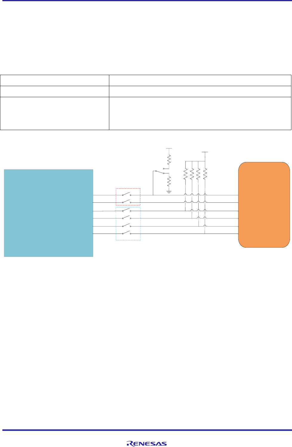
Hardware Design Specification
ASD-B-16-0247 Rev1.3 Page
33
of 105
September 8, 2017
RTK00V2XRC7746SFS
3.10.2 CPU JTAG2 debug
3.10.2.1 Specification
On the Tethys board, the R-Car W2H has the CPU JTAG2 debug interface. The SW12 switch 2-3 short is for normal operation
and 2-1 short for CPU JTAG2 debug
Table 13 CPU JTAG2 debug
Control Interface
CPU JTAG2
Debug Interface
CN4: IMSA-9632S-26Y801 from IRISO
operating conditions
The SW12 switch 2-1 short
The SW1 switch 9-8 short, switch 10-7 short
The SW2 switch 8-1 short, switch 7-2 short, switch 6-3 short, switch 5-4 short
3.10.2.2 Block Diagram
D1.8V
10K
R-Car W2H
U1
JTAG CN
CN4
D1.8V
10K
10K
SW12
3
1
2
MMC0_CMD_TRST
MMC0_D2_TDI
MMC0_D1_TMS
MMC0_D0_TCK
MMC0_D3_ASEBRK#/ACK
MMC0_CLK_TDO
5 4
36
7 2
8 1
SW2
9
10
8
7
SW1
GP0_15/MMC0_D0
GP0_16/MMC0_D1
GP0_17/MMC0_D2
GP0_18/MMC0_D3
GP0_13/MMC0_CLK
GP0_14/MMC0_CMD
Figure 11 Block Diagram of the CPU JTAG2 (SH-4AL) debug
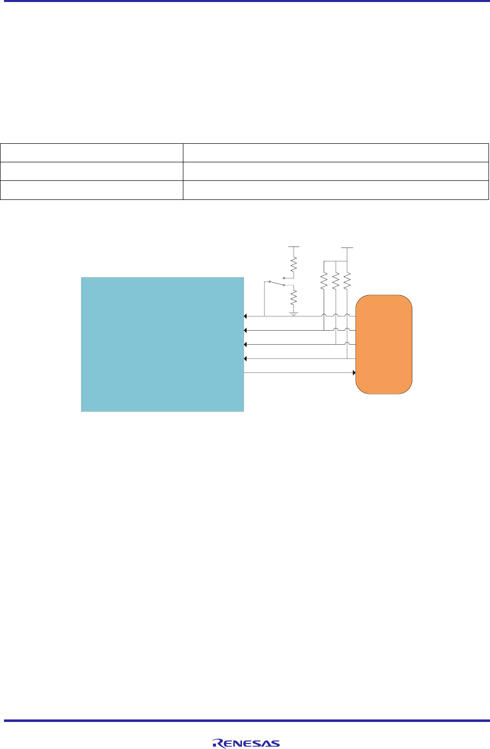
Hardware Design Specification
ASD-B-16-0247 Rev1.3 Page
34
of 105
September 8, 2017
RTK00V2XRC7746SFS
3.10.3 MCU debug
3.10.3.1 Specifications
On the Tethys board, the RH850 F1H / F1L has the JTAG interface and provides the serial programming function. The serial
programming function is used to test the connection between the devices mounted on the printed-circuit board. The SW17 switch 2-3
short is for normal operation and 2-1 short for MCU Debug.
Table 14 MCU debug Specification
Control Interface
MCU Debug
Debug Interface
CN4: IMSA-9632S-26Y801 from IRISO
operating conditions
The SW17 switch 2-1 short for MCU Debug
3.10.3.2 Block Diagram
DCUTCK
DCUTMS
DCUTRST
BU3.3V
DCUTDO
DCUTDI
4.7K
RH850F1H/F1L JTAG CN
CN4
BU3.3V
4.7K
1K
SW17
3
1
2
Figure 12 Block Diagram of the MCU debug
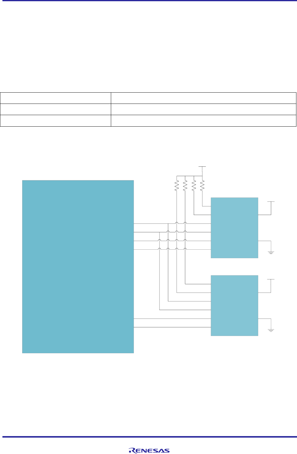
Hardware Design Specification
ASD-B-16-0247 Rev1.3 Page
35
of 105
September 8, 2017
RTK00V2XRC7746SFS
3.11 GYRO/G-SENSOR
3.11.1 Specifications
The A3G4250D manufactured by ST is a low-power 3-axis angular rate sensor able to provide unprecedented stability at zero
rate level and sensitivity over temperature and time. The AIS328DQ is an ultra low-power high performance 3-axis linear
accelerometer. The CPU communicates with the A3G4250D and AIS328DQ through its I2C1 and GPIOs.
Table 15 GYRO/G-SENSOR Specifications
Controller
R-Car W2H
Control Interface
The A3G4250D and AIS328DQ from ST
Supply voltage
D3.3V=3.3V
3.11.2 Block Diagram
SDO/SA0
CS
SCL
SDA
DRDY/INT2
INT1
SDO/SA0
CS
SCL
SDA
INT1
INT2
D3.3V
SCL1
SDA1
GP4_22
GP4_23
GP4_24
GP4_25
GYRO
A3G4250D
G-SENSOR
AIS328DQ
R-car W2H
10K
Figure 13 Block Diagram of the GYRO/G-SENSOR

Hardware Design Specification
ASD-B-16-0247 Rev1.3 Page
36
of 105
September 8, 2017
RTK00V2XRC7746SFS
3.12 I2C Interfaces
3.12.1 Specifications
The R-Car W2H incorporates five I2C interfaces (3.3 V). Since the R-Car W2H uses LVTTL-type I/O buffers on I2C interfaces, it
cannot directly drive an I2C bus with a relatively high load capacitance (e.g. 100 pF).
While the above restriction applies to interfaces of the R-Car W2H, the design of the Tethys board calls for multiple I2C devices
being connected to I2C interfaces 1. In order to compensate for the driving ability of the R-Car W2H, the Tethys board incorporates
an LTC4313IMS8-1#PBF I2C buffer manufactured by Linear Technology, through which each I2C device is connected to the I2C
interface for the device.
The following devices are connected to each I2C interface on the Tethys board.
Table 16 List of I2C Devices
I2C Controller
On-chip I2C controllers in the R-Car W2H
I2C devices through I2C interface 1
Through LTC4313IMS8-1#PBF (U2) from Linear Technology
U17: 24LC64EST from Microchip
U28: A3G4250D from ST
U29: AK4642EN from AKM
U30: AIS328DQ from ST
U32: RH850F1H/F1L from Renesas
CN11: 1759546-1 from TE for PCIE Express
CN14: HTST-103-04-S-D-RA from Samtec for HSM
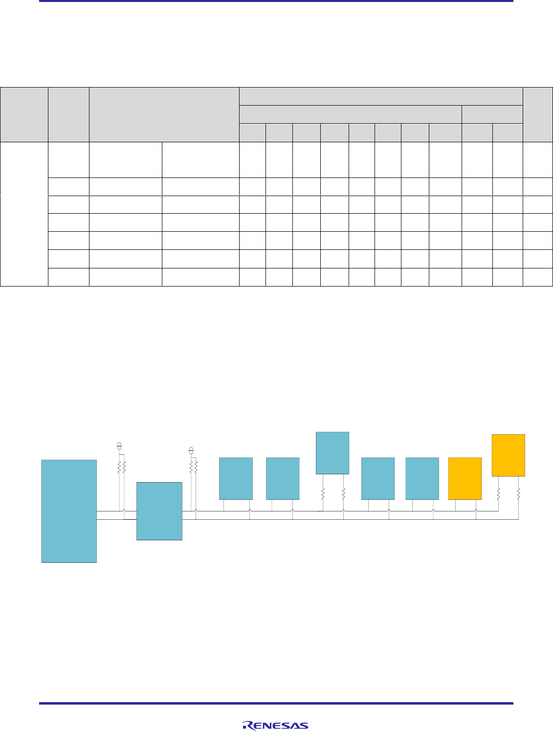
Hardware Design Specification
ASD-B-16-0247 Rev1.3 Page
37
of 105
September 8, 2017
RTK00V2XRC7746SFS
3.12.2 List of Slave Addresses
The table below lists the slave addresses of the I2C devices on the Tethys board
Table 17 List of I2C Slave Addresses
I2C
Interfaces
Ux/CNx
Device
Slave Addresses
Note
Binary
Hexadecimal
SA7
SA6
SA5
SA4
SA3
SA2
SA1
R/W#
RD
WR
1
U17
24LC64EST
I2C EEPROM for
MAC address
1
0
1
0
0
0
0
x
0xA1
0xA0
*1
U28
A3G4250D
GYRO
1
1
0
1
0
1
1
x
0xD7
0xD6
*2
U29
AK4642EN
AUDIO
0
0
1
0
0
1
0
x
0x25
0x24
*3
U30
AIS328DQ
G-SENSOR
0
0
1
1
0
0
1
x
0x33
0x32
*4
U32
RH850F1H/F1L
MCU
--
--
--
--
--
--
--
--
--
--
*5
CN11
Mini PCIE
Connector
--
--
--
--
--
--
--
--
--
--
CN14
HSM CN
Connector
--
--
--
--
--
--
--
--
--
--
-
Note:
*1 Pins 3 to 1 (A [2:0]) = GND
*2 Pin 8 to 12 (RESERVED [5:1]) = GND
*3 Pin 8 (CSN/CAD0) = GND
*4 Pin 25(EP) and Pin 4 (RESERVED1) = GND
*5 I2C no use
3.12.3 Block Diagram
U2
LTC4313IMS8-1#PBF
U1
R-Car W2H
SCL1_A
SDA1_A
SCL SDA
U17
24LC64EST
SCL SDA
U28
A3G4250D
U29
AK4642EN
SCL SDA
U30
AIS328DQ
SCL SDA
U32
RH850F1H/F1L
SCL SDA
CN14
HSM CN
SCL SDA
CN11
Mini PCIE
SCL SDA
0033 33
2K
1% 2K
1% 2K
1% 2K
1%
D3.3V D3.3V
Figure 14 Block Diagram of the I2C Interfaces
Hardware Design Specification
ASD-B-16-0247 Rev1.3 Page
38
of 105
September 8, 2017
RTK00V2XRC7746SFS
3.13 GPS Module
3.13.1 Specifications
The NEO-7P /7M/M8L manufactured by UBLOX is a high-performance GPS module. It has high performance active antenna.
It communicates with the CPU through the SCIF5 interface.
3.13.2 Block Diagram
GPS Receiver Module
NEO-7P/7M/M8L TXD
RXD SCIF5 R-Car W2H
CN7
U.FL-R-SMT
Hirose
GPS
Antenna
Figure 15 Block Diagram of the GPS module
Hardware Design Specification
ASD-B-16-0247 Rev1.3 Page
39
of 105
September 8, 2017
RTK00V2XRC7746SFS
3.14 CAN and Flexray Interface
3.14.1 Specifications
On the Tethys board, there are three CAN bus, one is connected to the R-Car W2H, and another two are connected to the MCU.
The high speed CAN driver TJA1050 manufactured by NXP is used for the two CAN bus.
On the Tethys board, there are one Flexray bus connected to the MCU. The high speed Flexray driver TJA1082 manufactured
by NXP is used for the Flexray bus.
Table 18 CAN and Flexray Interface Specifications
Controller
R-Car W2H and RH850F1H/F1L, if mounting RH850F1L, not Flexray function
Control Interface
CN6: HTST-105-04-S-D-RA from Samtec
CAN Transceiver Interface
TJA1050 from NXP
Flexray Transceiver Interface
TJA1082 from NXP
3.14.2 Block Diagram
CAN transceiver
TJA1050
NXP
U19
R-car W2H
CPU
U1
CAN transceiver
TJA1050
NXP
U21
RH850F1H/F1L
MCU
U32 CAN transceiver
TJA1050
NXP
U23
CN6
10 pin 2.54 pitch
connector
HTST-105-04-S-D-RA
Flexray transceiver
TJA1082
NXP
U47
Figure 16 Block Diagram of the CAN and Flexray Interface
Hardware Design Specification
ASD-B-16-0247 Rev1.3 Page
40
of 105
September 8, 2017
RTK00V2XRC7746SFS
The 10 pin connector (CN6) pin assignment is shown as below:
CN6 PIN Number
Signal
Remark
1
CPU_CAN0_H
HIGH-level CAN bus line
2
CPU_CAN0_L
LOW-level CAN bus line
3
MCU_CAN0_H
HIGH-level CAN bus line
4
MCU_CAN0_L
LOW-level CAN bus line
5
MCU_CAN1_H
HIGH-level CAN bus line
6
MCU_CAN1_L
LOW-level CAN bus line
7
BP
Flexray bus line plus
8
BM
Flexray bus line minus
9
GND
Ground
10
GND
Ground
Hardware Design Specification
ASD-B-16-0247 Rev1.3 Page
41
of 105
September 8, 2017
RTK00V2XRC7746SFS
3.15 LEDs and Switches
3.15.1 Specifications
The Tethys board incorporates four bits of tactile switches, and four bits of LEDs (eight LEDS for 4 GPIO place both top and
bottom side of the PCB) for debugging and status indication. They are connected to the GPIO pins of the R-Car W2H. Besides, there
are two LEDS control by the GPS 1PPS signal to indicate the GPS work status. The LED controlled by R-Car W2H port and GPS
1PPS signal correspondingly is shown as the table below,
LED
R-Car W2H PORT
Color
D3&D4
GP5_4
Green
D5&D6
GP5_5
Green
D7&D8
GP5_6
Green
D9&D10
GP5_7
Green
LED
Signal
Color
D11&D12
GPS_1PPS
Green
The tactile switch controlled by R-Car W2H or MCU port correspondingly is shown as the table below,
Tact SW
R-Car W2H or MCU PORT
SW13
GP5_0
SW14
GP5_1
SW15
GP5_2
SW16
GP5_3
SW4
MCU reset
There are other Switches are listed as below:
Table 19 DIP Switches default setting is as below table
DIP Switch
Description
Function
Default setting
ON(Short)
OFF(Open)
SW1
eMMC interface
and RL JTAG
Select switch
eMMC
JTAG
SW1: 1-16 short
SW1: 1-16 open
○
SW1: 2-15 short
SW1: 2-15 open
○
SW1: 3-14 short
SW1: 3-14 open
○
SW1: 4-13 short
SW1: 4-13 open
○
SW1: 5-12 short
SW1: 5-12 open
○
SW1: 6-11 short
SW1: 6-11 open
○
SW1: 7-10 open
SW1: 7-10 short
○
SW1: 8-9 open
SW1: 8-9 short
○
Hardware Design Specification
ASD-B-16-0247 Rev1.3 Page
42
of 105
September 8, 2017
RTK00V2XRC7746SFS
SW2
MMC interface and
RL JTAG Select
switch
JTAG
eMMC
SW2: 1-8 short
SW2: 1-8 open
○
SW2: 2-7 short
SW2: 2-7 open
○
SW2: 3-6 short
SW2: 3-6 open
○
SW2: 4-5 short
SW2: 4-5 open
○
SW5
Mode select switch
Mode=0
Mode=1
MD0
SW5: 1-16 short
SW5: 1-16 open
○
MD1
SW5: 2-15 short
SW5: 2-15 open
○
MD2
SW5: 3-14 short
SW5: 3-14 open
○
MD3
SW5: 4-13 short
SW5: 4-13 open
○
MD4
SW5: 5-12 short
SW5: 5-12 open
○
MD5
SW5: 6-11 short
SW5: 6-11 open
○
MD6
SW5: 7-10 short
SW5: 7-10 open
○
MD7
SW5: 8-9 short
SW5: 8-9 open
○
SW6
Mode select switch
Mode=0
Mode=1
MD8
SW6: 1-16 short
SW6: 1-16 open
○
MD9
SW6: 2-15 short
SW6: 2-15 open
○
MD10
SW6: 3-14 short
SW6: 3-14 open
○
MD11
SW6: 4-13 short
SW6: 4-13 open
○
MD13
SW6: 5-12 short
SW6: 5-12 open
○
MD14
SW6: 6-11 short
SW6: 6-11 open
○
MD20
SW6: 7-10 short
SW6: 7-10 open
○
MD21
SW6: 8-9 short
SW6: 8-9 open
○
SW7
Mode select switch
Mode=0
Mode=1
MDT0
SW7: 1-4 short
SW7: 1-4 open
○
MDT1
SW7: 2-3 short
SW7: 2-3 open
○
SW8
Ethernet MAC and
Ethernet AVB
Selected switch
Ethernet MAC
Ethernet/Ethernet AVB:
SW8: 1-8 short
SW8: 1-8 open
○
SW8: 2-7 short
SW8: 2-7 open
○
SW8: 3-6 short
SW8: 3-6 open
○
SW8: 4-5 short
SW8: 4-5 open
○
SW9
1.Ethernet MAC
and Ethernet AVB
Selected switch
2.512Mbit or
32Mbit SPI
FLASH Selected
Ethernet MAC
Ethernet/Ethernet AVB
SW9: 1-8 short
SW9: 1-8 open
○
SW9: 2-7 short
SW9: 2-7 open
○
SW9: 3-6 short
SW9: 3-6 open
○
SW9: 4-5 short
SW9: 4-5 open
○
QSPI0(512Mbit) Default
QSPI1 (32Mbit)
Hardware Design Specification
ASD-B-16-0247 Rev1.3 Page
43
of 105
September 8, 2017
RTK00V2XRC7746SFS
switch
SW9 : 3-6 short
SW9 : 3-6 open
○
SW9 : 4-5 open
SW9 : 4-5 short
○
SW10
Ethernet MAC and
Ethernet AVB
Selected switch
Ethernet/Ethernet AVB
Ethernet MAC
SW10: 1-8 open
SW10: 1-8 short
○
SW10: 2-7 open
SW10: 2-7 short
○
SW10: 3-6 open
SW10: 3-6 short
○
SW10: 4-5 open
SW10: 4-5 short
○
SW11
Ethernet MAC and
Ethernet AVB
Selected switch
Ethernet/Ethernet AVB
Ethernet MAC
SW11: 1-4 open
SW11: 1-4 short
○
SW11: 2-3 open
SW11: 2-3 short
○
Table 20 Slide Switches default setting is as below table:
Slide Switch
Description
Function
Default setting
ON(Short)
OFF(Open)
SW3
JTAG Debug/Normal
Operation select switch
JTAG Debug
Normal operation
SW3: 1-2 short
SW3: 1-2 open
○
SW3: 2-3 open
SW3: 2-3 short
○
SW12
JTAG Debug/Normal
Operation select switch
JTAG2 Debug
Normal operation
SW12: 1-2 short
SW12: 1-2 open
○
SW12: 2-3 open
SW12: 2-3 short
○
SW17
JTAG Debug/Normal
Operation select switch
MCU JTAG Debug
Normal operation
SW17: 1-2 short
SW17: 1-2 open
○
SW17: 2-3 open
SW17: 2-3 short
○
SW18
Power switch
System power
ON
OFF
SW18: 2-3 short
SW18: 2-3 open
○
SW18: 1-2 open
SW18: 1-2 short
○
Hardware Design Specification
ASD-B-16-0247 Rev1.3 Page
44
of 105
September 8, 2017
RTK00V2XRC7746SFS
3.16 Connection between CPU and MCU
3.16.1 Specifications
The Tethys board have a MCU to control the Power sequence and Reset sequence. The power sequence and reset sequence are shown
as Figure 23 and Figure 21 respectively in the next chapter.
The Tethys and MCU connection include MSIOF0 and I2C1 and RESET signal. The corresponding signals are shown as below:
HSCIF2 connection:
R-Car-W2H
Signal
MCU signal
MSIOF0_RXD_A
P11_9/CSIG1SO/RLIN35RX/INTP15/PWGA49O/TAUB1I13/TAUB1O13/MEMC0CS1
MSIOF0_SCK_A
P11_10/CSIG1SC/PWGA50O/TAUB1I15/TAUB1O15/MEMC0CS2/ETNB0COL
MSIOF0_TXD_A
P11_11/CSIG1SI/RLIN25TX/PWGA51O/TAUB1I0/TAUB1O0/MEMC0CS3/ETNB0RXDV
I2C connection:
R-Car-W2H
Signal
MCU signal
I2C1-SDA
P0_11/RIIC0SDA/DPIN12/CSIH1CSS2/TAUB0I8/TAUB0O8/RLIN26RX/PWGA34O
I2C1-SCL
P0_12/RIIC0SCL/DPIN13/PWGA45O/TAUB0I10/TAUB0O10/CSIG0SI/RLIN26TX
The CPU reset signal is controlled by MCU GPIO. That is P1_0/RLIN33RX/INTP13.
3.16.2 Block Diagram
Rcar-W2H
MSIOF
I2C1
RESET
MSIOF1_B
I2C1
RESET
MCU
RH850F1H/F1L
RIIC0
RESET
RLIN
Figure 17 Block Diagram of the Connection between CPU and MCU
Hardware Design Specification
ASD-B-16-0247 Rev1.3 Page
45
of 105
September 8, 2017
RTK00V2XRC7746SFS
3.17 Clock system
The Tethys board uses the crystal oscillators and resonators shown below.
3.17.1 Clock Signals Supplied to the R-Car W2H
Table 21 List of Clock Signals and Crystals for the R-Car W2H
NO.
Xn
Supply voltage
R-Car W2H pin name
Frequency
Description
Part number
Manufacturer
Type
1
X1
3.3V
GP1_22/EX_WAIT0/CAN_
CLK_B/SCIF_CLK_A
14.7456MHz
SCIF clock
SG-8003CE14.7456
00MHzPCL
Epson
Oscillator
2
X2
3.3V
GP3_11/RX0_B/SCL0_C/A
VB_GTXREFCLK/ETH_M
DC
125.00MHz
AVB_GTXREF
CLK
SG-8003CE125.000
000MHzPCL
Epson
Oscillator
3
Y1
USB_XTAL ,
USB_EXTAL
48MHz
USB clock
FA-238A48.000MH
z10
Epson
Crystal
4
Y2
-
XTAL , EXTAL
20.00MHz
CPU main clock
FA-238A20.000000
MHz10
Epson
Crystal
3.17.2 Differential Clock Signals Supplied to the R-Car W2H
Table 22 List of Differential Clock Signals Supplied to the R-Car W2H
NO.
R-Car W2H Pin Assignment
R-Car W2H pin name
Clock Driver Pin Name
Signal Type
1
AC12
CLKP
REFCLK-
Differential signal
2
AB12
CLKN
REFCLK+
3.17.3 Clock Signals Supplied to Devices Other than R-Car W2H
Table 23 List of Clocks and Crystals other than for R-Car W2H
NO.
Xn
Device
Device pin name
Frequency
Description
Part number
Manufacturer
Type
1
X3
AK4642EN
MCKI
12.288MHz
Audio Clock
SG-8003CE12.2880
00MHzPCL
Epson
Oscillator
2
Y3
GL852GT(USB Hub)
X1 , X2
12MHz
USB Hub Clock
FA-238A12.000000
MHz10
Epson
Crystal
3
Y4
KSZ8041RNLI
XI , XO
25MHz
Ethernet clock
FA-238A25.0000M
Hz18
Epson
Crystal
4
Y5
RH850F1H/F1L
X1 , X2
12MHz
MCU main clock
FA-238A12.000000
MHz10
Epson
Crystal
5
Y6
RH850F1H/F1L
XT1 , XT2
32.768kHz
MCU sub clock
FC-13A32.768000k
Hz12.5
Epson
Crystal
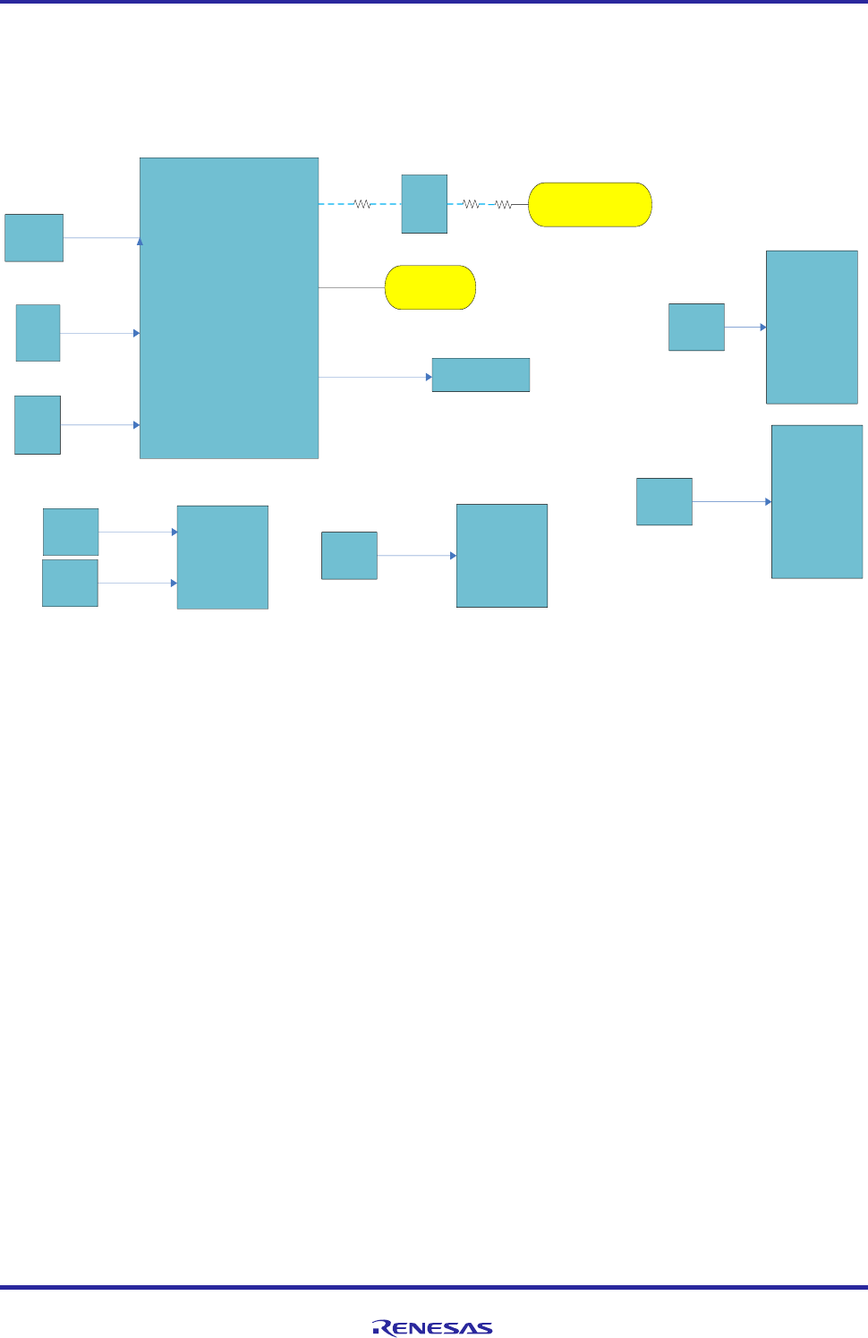
Hardware Design Specification
ASD-B-16-0247 Rev1.3 Page
46
of 105
September 8, 2017
RTK00V2XRC7746SFS
3.17.4 Block Diagram
Y1
Crystal
48MHz
Y2
Crystal
20MHz
U1
R-Car W2H
U3、U4
DDR3 x 2psc
PCIE CON
CN11
X1
OSC
14.7456MHz
U32
RH850F1H/F1L
Y5
Crystal
12MHz
U29
AK4642EN
X3
OSC
12.288MHz
Y6
Crystal
32.768KHz U16
KSZ8041RNLI
Y4
Crystal
25MHz
X2
OSC
125MHz
N.M.
U14
GL852GT-MNGXX
Y3
Crystal
12MHz
0
Mini PCIE Connector for
EtherAVB Sub Board
CN8
N.M.
22 33
Figure 18 Block Diagram of the Clock system
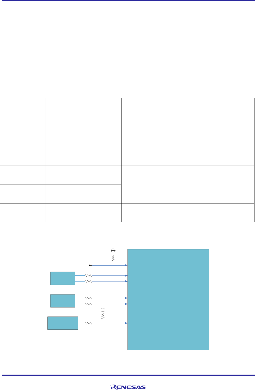
Hardware Design Specification
ASD-B-16-0247 Rev1.3 Page
47
of 105
September 8, 2017
RTK00V2XRC7746SFS
3.18 External Interrupts
3.18.1 Specifications
The R-Car W2H has external interrupt input pins which are NMI, GP4_22, GP4_23, GP4_24, GP4_25, and GP5_8. For details on the
external interrupts, please refer to the R-Car W2H Hardware Manual.
The Tethys board uses NMI as external interrupt input pin, GP4_22, GP4_23, GP4_24, GP4_25, and GP5_8 as GPIO interrupts.
These pins should be used as active-low signals in programs.
The devices and connectors of the interrupt request sources on the Tethys board are shown below table 24.
Table 24 External Interrupts Specifications
Interrupt Pin
Other pin function
Devices that Output Interrupt Request
Connectors
NMI
——
Test point
TP5
——
GP4_22
RX3_A/SCL1_C/MSIOF1_RXD_B
/AUDIO_CLKA_C/SSI_SDATA4_B
GYRO
U28 A3G4250D from ST
——
GP4_23
TX3_A/SDA1_C/MSIOF1_TXD_B
/AUDIO_CLKB_C/SSI_WS4_B
GP4_24
SCL2_A/MSIOF1_SCK_B
/AUDIO_CLKC_C/SSI_SCK4_B
G-SENSOR
U30 AIS328DQ from ST
——
GP4_25
SDA2_A/MSIOF1_SYNC_B
/AUDIO_CLKOUT_C
GP5_8/IRQS#
SSI_SDATA7_A/
AUDIO_CLKA_D/CAN_CLK_D
ETHERNET
KSZ8041RNLI from Micrel
——
3.18.2 Block Diagram
U1
R-Car W2H
NMI
D3.3V
TP5
Test point
GP4_22
GP4_23
U28
GYRO
A3G4250D
0
0
GP4_24
GP4_25
0
0
U30
G-SENSOR
AIS328DQ
GP5_8/IRQ8#
0
U16
ETHERNET
KSZ8041RNLI
10K
D3.3V_ETH
Figure 19 Block Diagram of the External Interrupts
Hardware Design Specification
ASD-B-16-0247 Rev1.3 Page
48
of 105
September 8, 2017
RTK00V2XRC7746SFS
3.19 Reset System
3.19.1 Specifications
On the Tethys board, the MCU power-on reset signal is cleared by the reset IC TPS3808G01DBVT, 389ms after the D3.3V
power supply has settled. Also a power-on reset signal can be generated by pushing the push switch (SW4). The reset signal is
level-shifted from 3.3 V to 1.8 V by the HD74LV1G08ACME and is input to the PRESET# pin of the R-Car W2HR-Car W2H.
Table 25 Reset System Specifications
Reset IC
TPS3808G01DBVT from TI
Threshold voltage: 1.7415V
Reset delay time : 389ms (Reset delay time=CT ( nF )/175+0.0005 (s ) )
3.19.2 Block Diagram
U32
MCU
RH850F1H/F1L
CN4
MCU JTAG
IMSA-9632S-26Y801
U8
Reset IC
TPS3808G01DBVT
MR#
BU3.3V
SOC_RST
U5
SPI FLASH
S25FL512SAGMFIG11
SYS_RESETn_33
U7
EMMC
SDIN8DE1-8G-XA
CN4
CPU JTAG
IMSA-9632S-26Y801
U1
R-CarW2H
SYS_RESETn_18
DDR3*2( U3、U4)
MT41K256M16HA-125
AAT:E
CN9
Mini PCIE CN
1759546-1
VDD
BU3.3V
D3.3V
CN8
Mini PCIE CN
1759546-1
CN12
Mini PCIE CN
1759546-1
U16
ETHERNET
KSZ8041RNLI
D1.8V
10K
ResetB
ResetB
ResetB
M0RESET#
RST#
RST_n
RESET
#
RESET#
PRESET#
0
10K
U14
USB HUB
GL852GT-MNGXX
U29
AUDIO CODEC
AK4642EN
SW4
U36
DCDC
R2A11301FT
U9
HD74LV1G08ACME
IN_A
IN_B OUT_Y
VCC
Figure 20 Block Diagram of the Reset System
MCU_RESETn
Hardware Design Specification
ASD-B-16-0247 Rev1.3 Page
49
of 105
September 8, 2017
RTK00V2XRC7746SFS
3.19.3 Reset Sequence
The Reset sequence is shown below:
BU5.0V
BU3.3V
MCU_RESETn
P5.0V
P3.3V
VSYS
D1.8V
SOC_D18PWGD
D1.0V
D1.5V
VREF/VTT
SOC_D10PWGD
D3.3V
D5.0V
SOC_RST(MCU)
1ms min
Reset sequence
SOC_PWRON(MCU)
Reset time
3ms
2ms
2ms
1us min
MCU boot
Figure 21 The Reset Sequence
Hardware Design Specification
ASD-B-16-0247 Rev1.3 Page
50
of 105
September 8, 2017
RTK00V2XRC7746SFS
3.20 Power system
3.20.1 Specifications
The Tethys board operates on a single BU12V power supply. The power supplies used for the Tethys board are generated by the
switching regulators and low-dropout regulators. Because the maximum output current of the AC adapter attached for Tethys board
is 3A at 12v input status, please make sure not to exceed 3A for all sub-board inserted in extending interface connector such as mini
PCIE etc. If end user need more current AC adapter, please prepare over 6A/12V stable AC adapter by end user.
Table 26 List of the Switching Controllers and Regulators on the Tethys Board
Vin
Vout
Switching Controller/Regulator
Power MOSFET
ACC Switch Control
Power Supply BU12V
Through CN17 or CN18 (1*)
BU12.0V
_________
_________
Not supported
BU12.0V
VSYS
Renesas
R2A11301FT (U36)
Renesas
HAT2210R
(U35 and U37)
supported
BU5.0V
supported
P3.3V
supported
PCIE_5.0V
Texas Instruments
TPS54531DDA(U26)
supported
VSYS
P5.0V
Vishay Siliconix
Si3433CDV-T1-E3(U34)
supported
BU5.0V
BU3.3V
RICOH
RP111N331D-TR-AE(U33)
supported
P3.3V
D3.3V
Vishay Siliconix
SI3433CDV-T1-E3(U40)
supported
D1.5V
Texas Instruments
TPS3808G01DBVT(U45)
supported
D2.5V
RICOH
RP111N251D-TR-AE(U46)
supported
P5.0V
D1.2V
Texas Instruments
TPS54531DDA(U44)
supported
D1.8V
SEMTECH
SC183CULTRT(U38)
supported
D5.0V
Vishay Siliconix
Si3433CDV-T1-E3(U43)
supported
D3.3V
VCCQ_SD2
RICOH
RP111N181D-TR-AE(U12)
supported
VCCQ_SD0
Vishay Siliconix
Supported
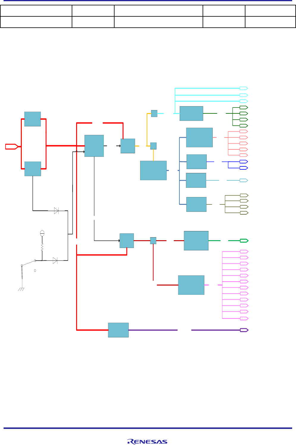
Hardware Design Specification
ASD-B-16-0247 Rev1.3 Page
51
of 105
September 8, 2017
RTK00V2XRC7746SFS
SI3433CDV-T1-E3(U13)
BU3.3V
BU3.3V_MCU
supported
(1*) CN17 and CN18 are 12V power connectors, use can choose one connector according to the demand
3.20.2 Block Diagram
R2A11301FT
MOS FET
HAT2210R
MOS FET
HAT2210R
Gate Ctrl
Gate Ctrl
BU12V
FB
FB
VSYS
FB
BU12V
RP111N331D-TR-AE
BU5.0V
MOSFET(Power Switch)
Si3433CDV-T1-E3
BU3.3V Flexray transceiver(max:350mA)
MCU
Flexray transceiver (max:350mA)
MCU CAN (max:75mA)
MCU CAN (max:75mA)
MOSFET(Power Switch)
Si3433CDV-T1-E3
CPU CAN transceiver(max:75mA)
To USB Host Type A Receptacle(max:500mA)
To USB Host Type A Receptacle(max:500mA)
To USB HUB: GL852GT-MNGXX(max:100mA)
RP111N251D-TR-AE
P3.3V D2.5V Main CPU(max:400mA)
MOSFET(Power Switch)
Si3433CDV-T1-E3
P3.3V
[LED (max:10mA)]X10
SC183CULTRT
TPS54531DDA
LM3102MH
Main CPU(max:120mA)
Micro SD slot(max:100mA)
D1.2V Main CPU(max:3525mA)
D1.5V
Main CPU(max:450mA)
DDR3(max:360mA)
DDR3(max:360mA)
PCIE CN(max:375mA)
Main CPU(max:324mA)
SPI Flash(max:100mA)
SPI Flash(max:100mA)
GPS Receive(Max:63mA)
RMII PHY(min:53mA)
EMMC(max:300mA)
GYRO(max:7mA)
G-SENSOR(max:450uA)
AUDIO Codec(max:167mA)
Micro SD slot(max:100mA)
PCIE CN(max:1000mA)
D3.3V
TPS54531DDA [PCIE CN(max:1500mA)]X3
P5.0V
D5.0V
D1.8V
PCIE_5.0V
BU12V
CN18
HEC0470-01-
630(MJ-179P)
CN17
34793-9040
SW18 1
3
2
SW18:2-3 short: ON
1-2 short: OFF
ACC_CONT_EXT
ACC_CONT_EXT
BU12V
EN1/EN2
MCU reset (max:0.005mA)
CPU and MCU JTAG
HSM CN
Figure 22 Block Diagram of the Power System
Hardware Design Specification
ASD-B-16-0247 Rev1.3 Page
52
of 105
September 8, 2017
RTK00V2XRC7746SFS
3.20.3 Power Sequence
There are no restrictions on the power-on sequence. Ensure that all other power supplies rise from the ground (VSS**)
within 300 ms of any single power supply rising from the ground (VSS**). We do power up sequence as the Tethys power up
sequence. The diagram of the sequence for turning on the power to the Tethys board is shown as below
BU5.0V
BU3.3V
VSYS
P5.0V
P3.3V
SOC_PWRON(MCU)
D1.8V
SOC_D18PWGD
D1.0V
D1.5V
VREF/VTT
SOC_D10PWGD
D3.3V
D5.0V
SOC_RST(MCU)
1ms min
3ms
2ms
2ms
1um min
Power on sequence
300ms max
Figure 23 The Power Sequence
There are no restrictions on the power-off sequence. Ensure that all other power supplies fall to the ground (VSS**)
level within 300 ms of any single power supply being turned off. We do the power off sequence as the Tethys power off sequence,
turn off the power supplies in reverse order of the power-on sequence.
Hardware Design Specification
ASD-B-16-0247 Rev1.3 Page
53
of 105
September 8, 2017
RTK00V2XRC7746SFS
4 Memory map
4.1 Specifications
Memory map for R-Car W2H boot loader is shown below. The maximum size of U-Boot is the value that
subtracted Initialization stack from 240Kbytes. The maximum size of initialization stack is 256Kbytes.
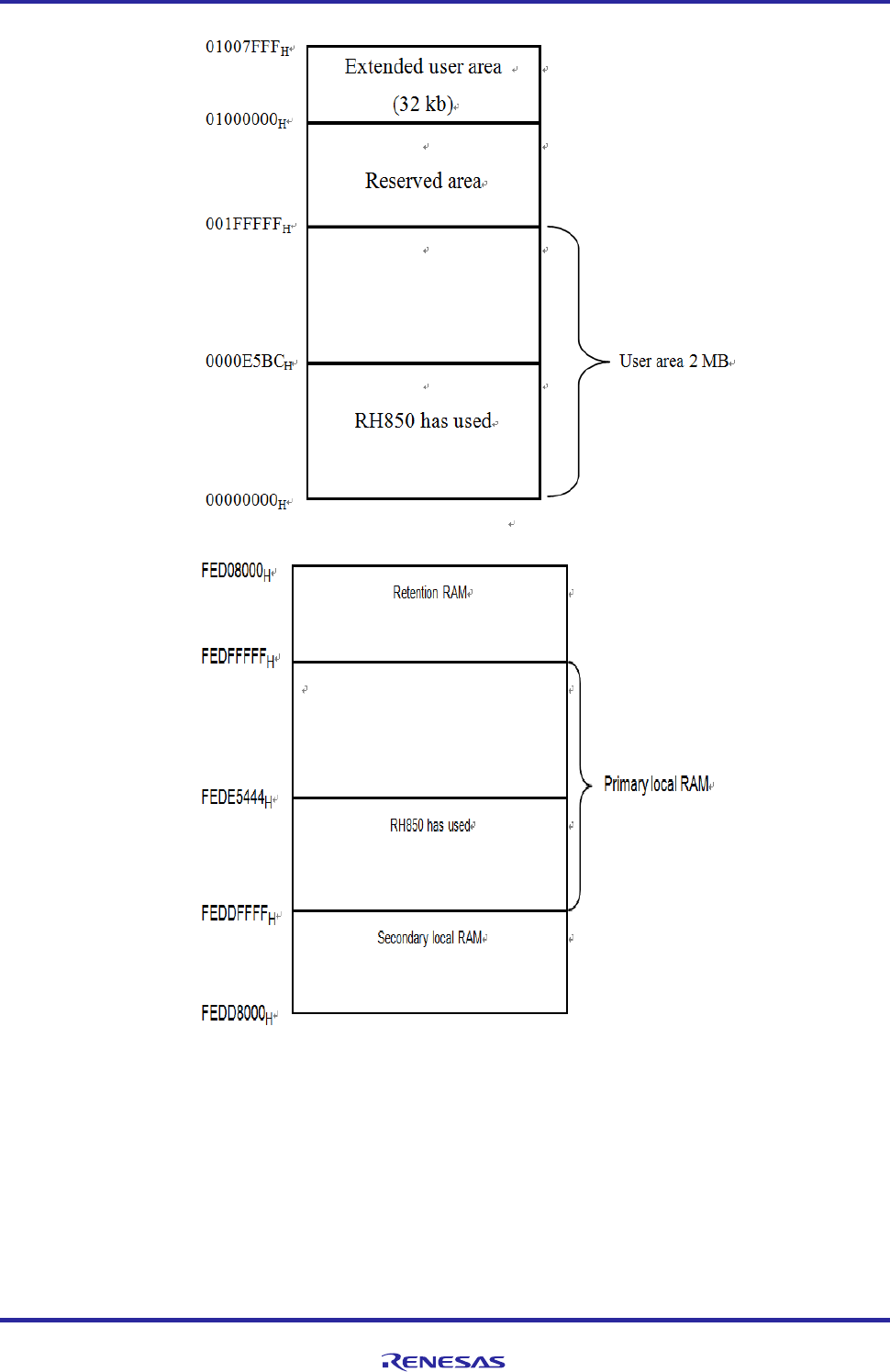
Hardware Design Specification
ASD-B-16-0247 Rev1.3 Page
54
of 105
September 8, 2017
RTK00V2XRC7746SFS
Memory map for RH850F1H/F1L is shown in the above figure. The user area of the code flash memory of
the RH850F1H/F1L is 2MB. A single block of 32-Kbyte extended user area is also incorporated.
RH8500F1H/F1L includes three types of the local RAM: Primary local RAM, Secondary local RAM, Retention
RAM. RH850’s data memory uses Primary local RAM which is RAM area that can be accessed with speed.
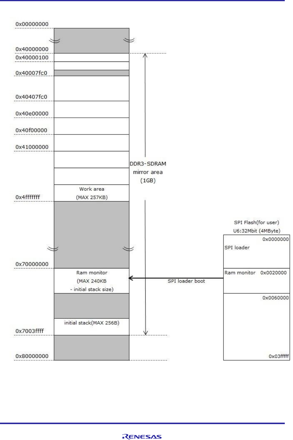
Hardware Design Specification
ASD-B-16-0247 Rev1.3 Page
55
of 105
September 8, 2017
RTK00V2XRC7746SFS
Memory map for 32MB SPI flash is shown below:
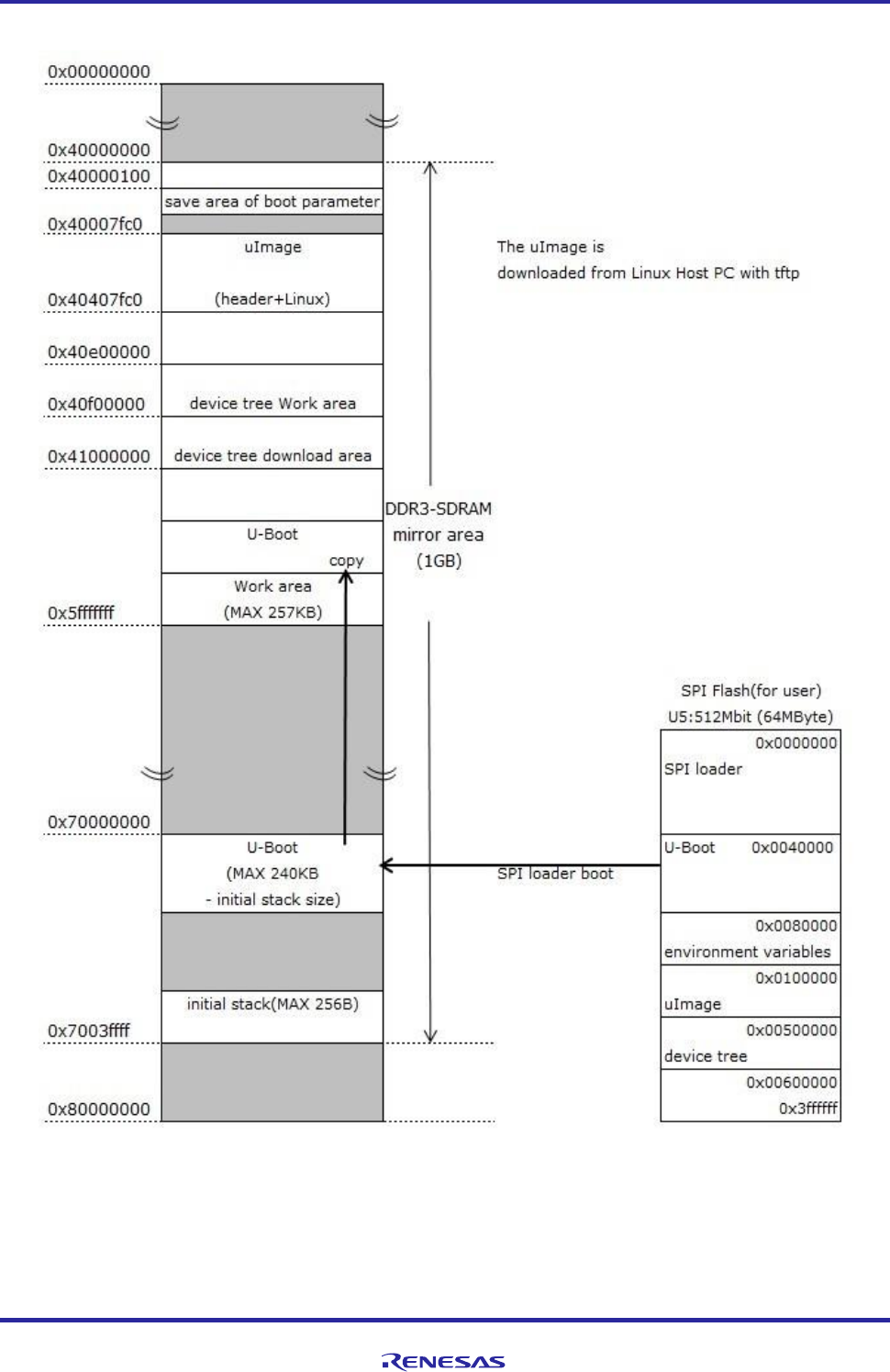
Hardware Design Specification
ASD-B-16-0247 Rev1.3 Page
56
of 105
September 8, 2017
RTK00V2XRC7746SFS
Memory map for 512MB SPI flash is shown below:
Hardware Design Specification
ASD-B-16-0247 Rev1.3 Page
57
of 105
September 8, 2017
RTK00V2XRC7746SFS
4.2 Function
These codes of RH850 have realized four functions as follows.
4.2.1 Control the power of the Tethys Custom Board.
The flow chart is as follows:
Delay 300ms (max)
Pull up SOC_RST
END
YES
NO
START
Pull down the SOC_RST
and SOC_PWRON
Pull up
SOC_PWRO
N
SOC_PWRON has
been pulled up
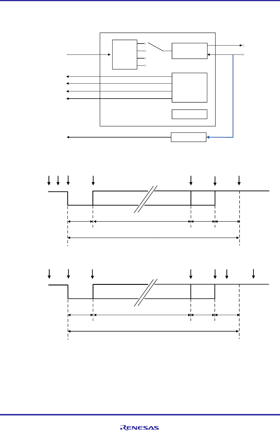
Hardware Design Specification
ASD-B-16-0247 Rev1.3 Page
58
of 105
September 8, 2017
RTK00V2XRC7746SFS
4.2.2 Realize the UART with the baud rate of 115200
This UART uses RLIN31 of RH850’s LIN/UART interface.
Edge detection circuit
RLIN3nTX
RLIN3nRX
LINn registers
LINn interrupt
controller circuit
LINn baud rate
generator
Protocol
controller
LIN communication
clock source
INTRLIN3nUR0
INTRLIN3nUR1
INTRLIN3nUR2
INTRLIN3n
INTP1n
RLIN3n
Figure shows LIN/UART interface (in UART mode) transmission operations as follows
Start bit
(1)(2)(3) (4) (5)(6)(7)
Idle Idle
7 , 8, or 9 data bits
0 or 1
parity bit
1 or 2
stop bits
UART frame
RLIN3nTX
Figure shows the LIN/UART interface (in UART mode) reception operation as follows.
(1)(2)(3)(4) (5)(6)(7)
Idle Idle
7 , 8, or 9 data bits
0 or 1
parity bit
1 or 2
stop bits
UART frame
RLIN3nTX
(about [NSPB], [IBS]’s definition, please refer to [r01uh0445ej0100_rh850f1h.pdf] page 937,859’s description).
This UART’s operations are as follows:
1. 15: The NSPB bits select the number of sampling in one Tbit (reciprocal of the bit rate).
2. Noise filter ON: The noise filter is enabled when receiving data
3. Non-parity, 8bit, 1stop.
4. No space: The IBS bits set the width of the space between the UART frame in UART buffer transmit
Hardware Design Specification
ASD-B-16-0247 Rev1.3 Page
59
of 105
September 8, 2017
RTK00V2XRC7746SFS
4.2.3 Realize an asynchronous serial with baud rate of 1M between RH850 and CPU.
This UART uses RLIN30 of RH850’s LIN/UART interface. The operations are same as above.
4.2.4 Make CAN0 and CAN1 working with baud rate of 1M
1. CAN0 sends 4-byte data only once.
2. CAN1 receives the data coming from CAN0.
3. Once CAN1 receives, the wave form can not be monitored.
The flow chart is as follows
YES
END
NO
START
Initialize can0
and can1
Can0 sends
4-byte data
Can1 has received
the data
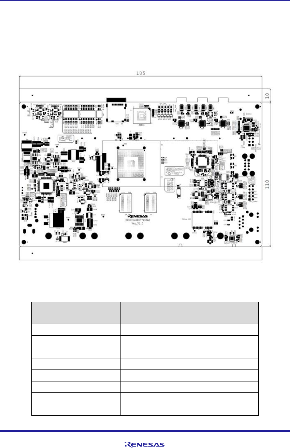
Hardware Design Specification
ASD-B-16-0247 Rev1.3 Page
60
of 105
September 8, 2017
RTK00V2XRC7746SFS
5 Outline Diagrams of the Tethys Board
5.1 Tethys Board dimension
The Tethys board dimension is shown as below (Unit: mm):
Board: 1.6 mm
Board: 8 Layers
Figure 24 The Tethys board dimension
5.2 The weight of the Tethys Board
Condition
Weight (Unit : g)
Screw (total)
4
Spacer (two piece)
4
Shell
165
Heat dissipation silica gel
4
Board
143
RF Cable (15cm, four piece)
16
RF Cable (20cm, one piece)
5
Tethys assembly(total)
341
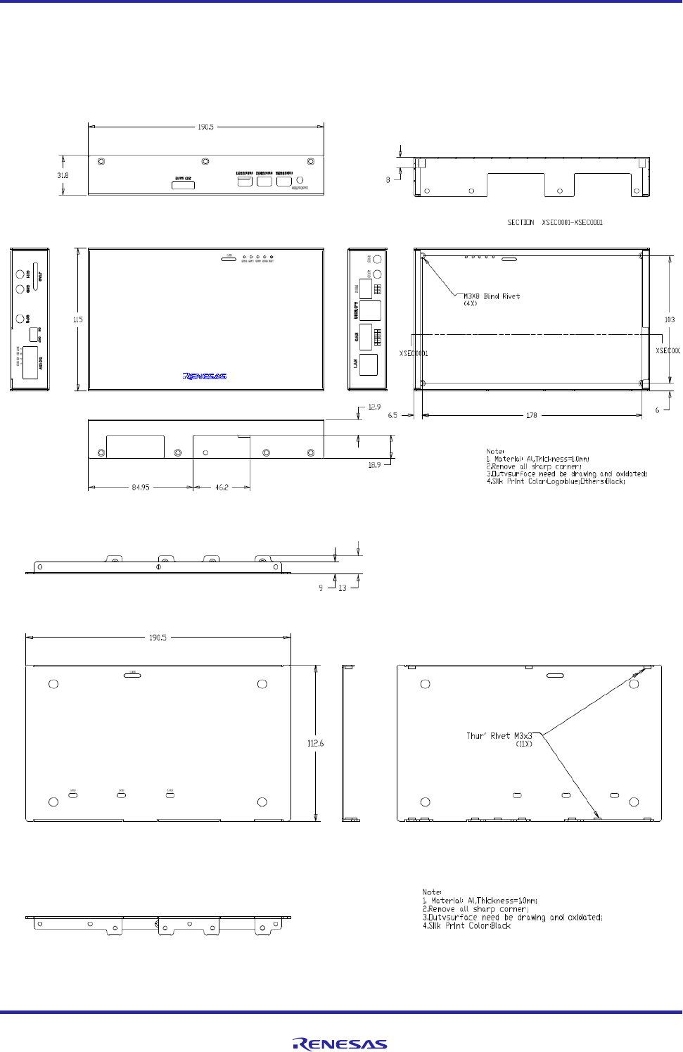
Hardware Design Specification
ASD-B-16-0247 Rev1.3 Page
61
of 105
September 8, 2017
RTK00V2XRC7746SFS
5.3 Tethys ID dimension
The ID of Tethys board dimension is shown as below (Unit: mm):
Base Panel size
Cover Panel size:
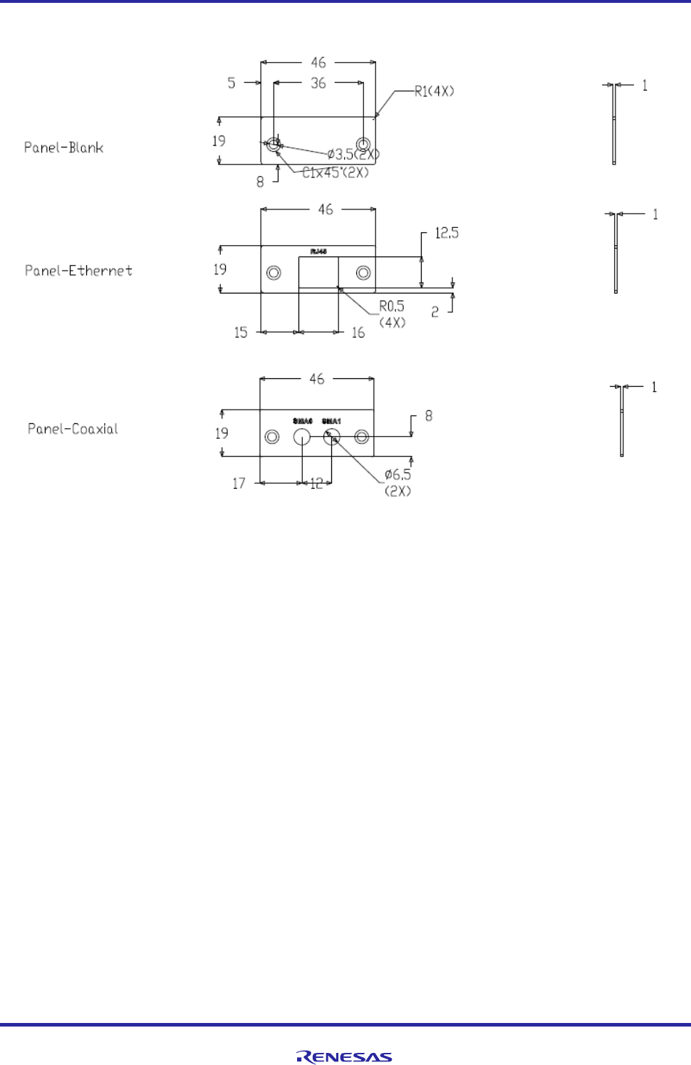
Hardware Design Specification
ASD-B-16-0247 Rev1.3 Page
62
of 105
September 8, 2017
RTK00V2XRC7746SFS
Side Cover size (Option)
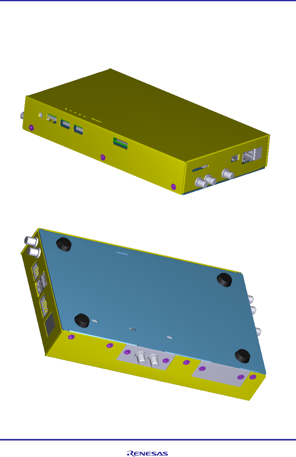
Hardware Design Specification
ASD-B-16-0247 Rev1.3 Page
63
of 105
September 8, 2017
RTK00V2XRC7746SFS
5.4 Tethys assembly
The assembly pictures of Tethys board are shown as below
Top side view:
Bottom side view:
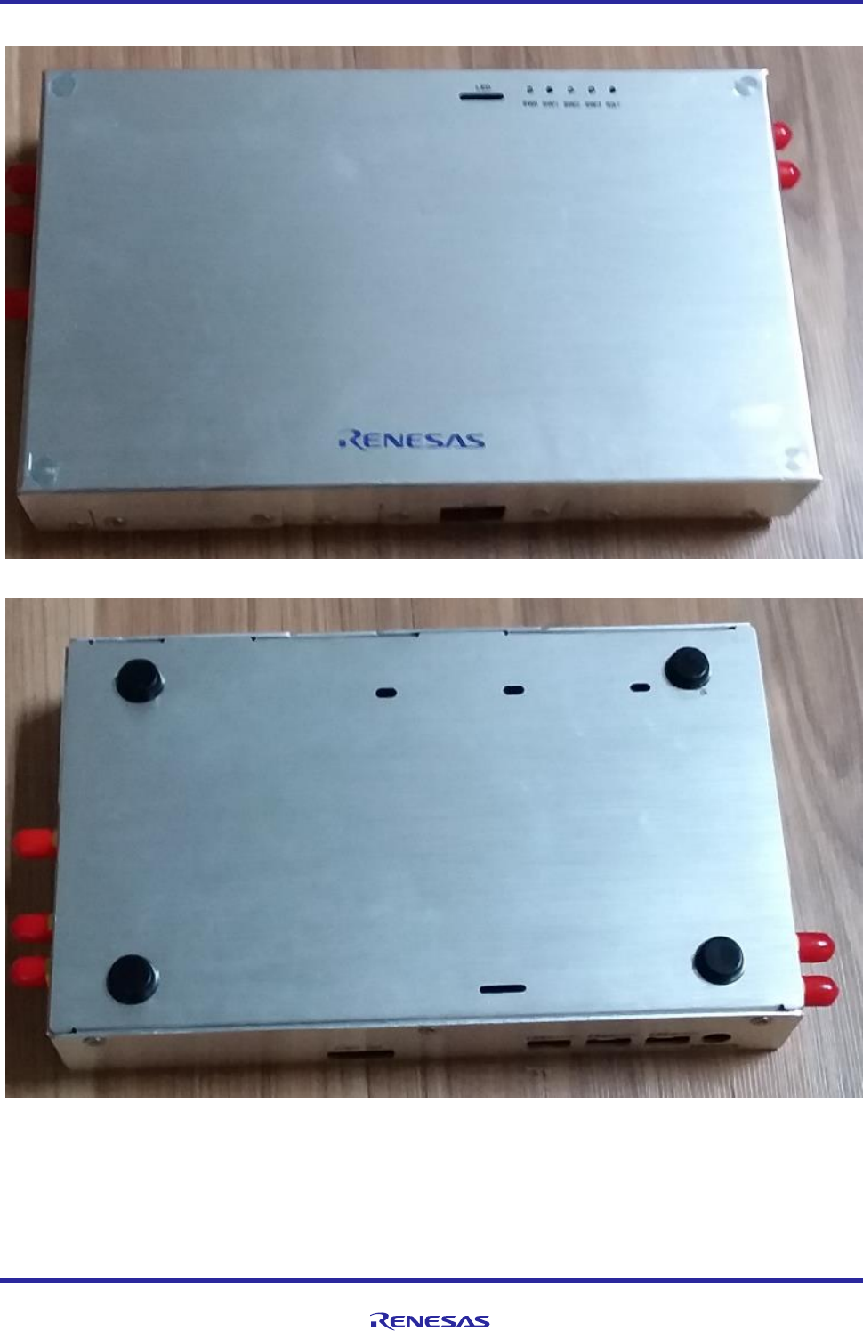
Hardware Design Specification
ASD-B-16-0247 Rev1.3 Page
64
of 105
September 8, 2017
RTK00V2XRC7746SFS
Top Side View:
Bottom Side View:
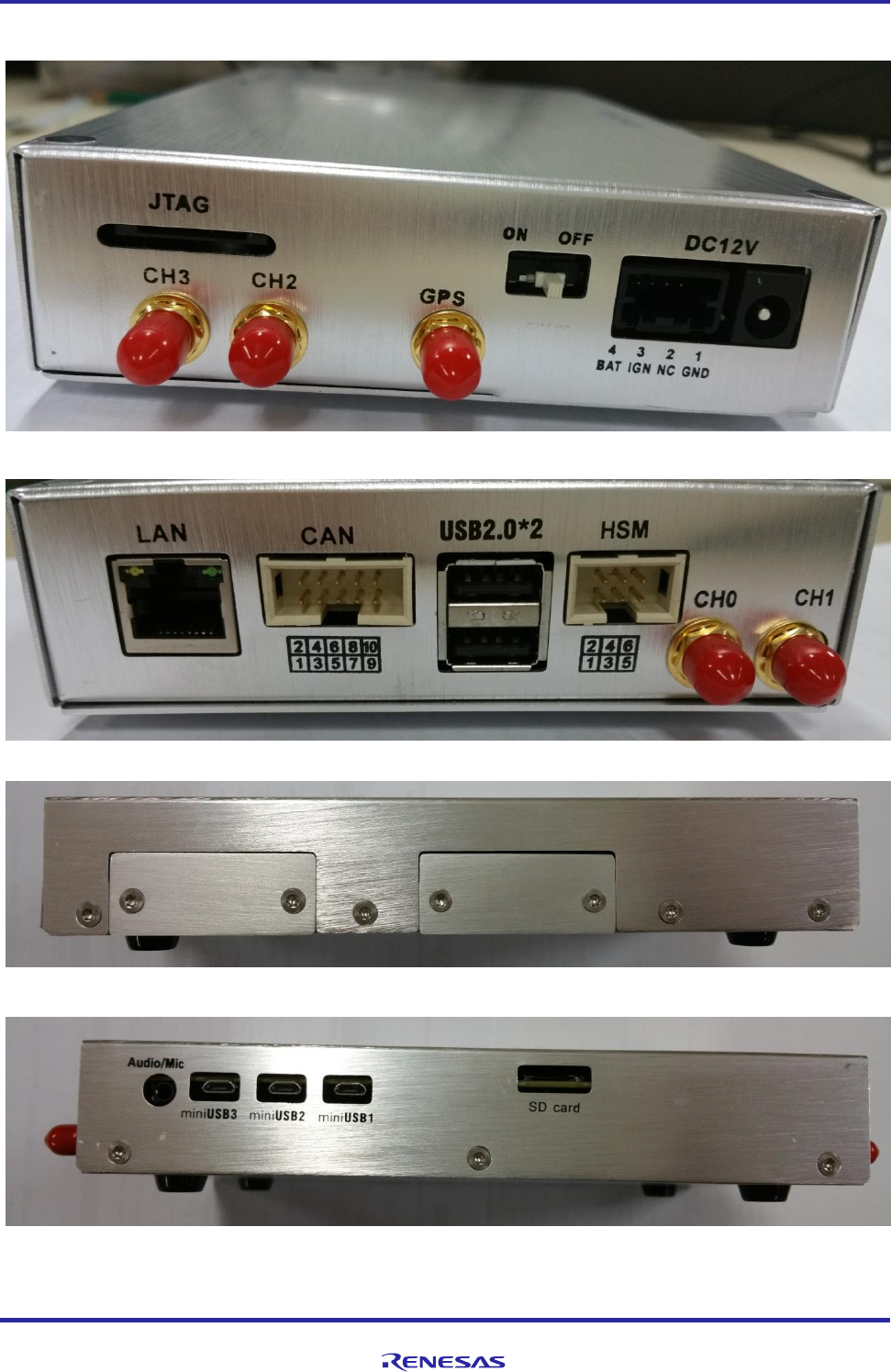
Hardware Design Specification
ASD-B-16-0247 Rev1.3 Page
65
of 105
September 8, 2017
RTK00V2XRC7746SFS
Left Side View
Right View Side
Front Side View
Back Side View
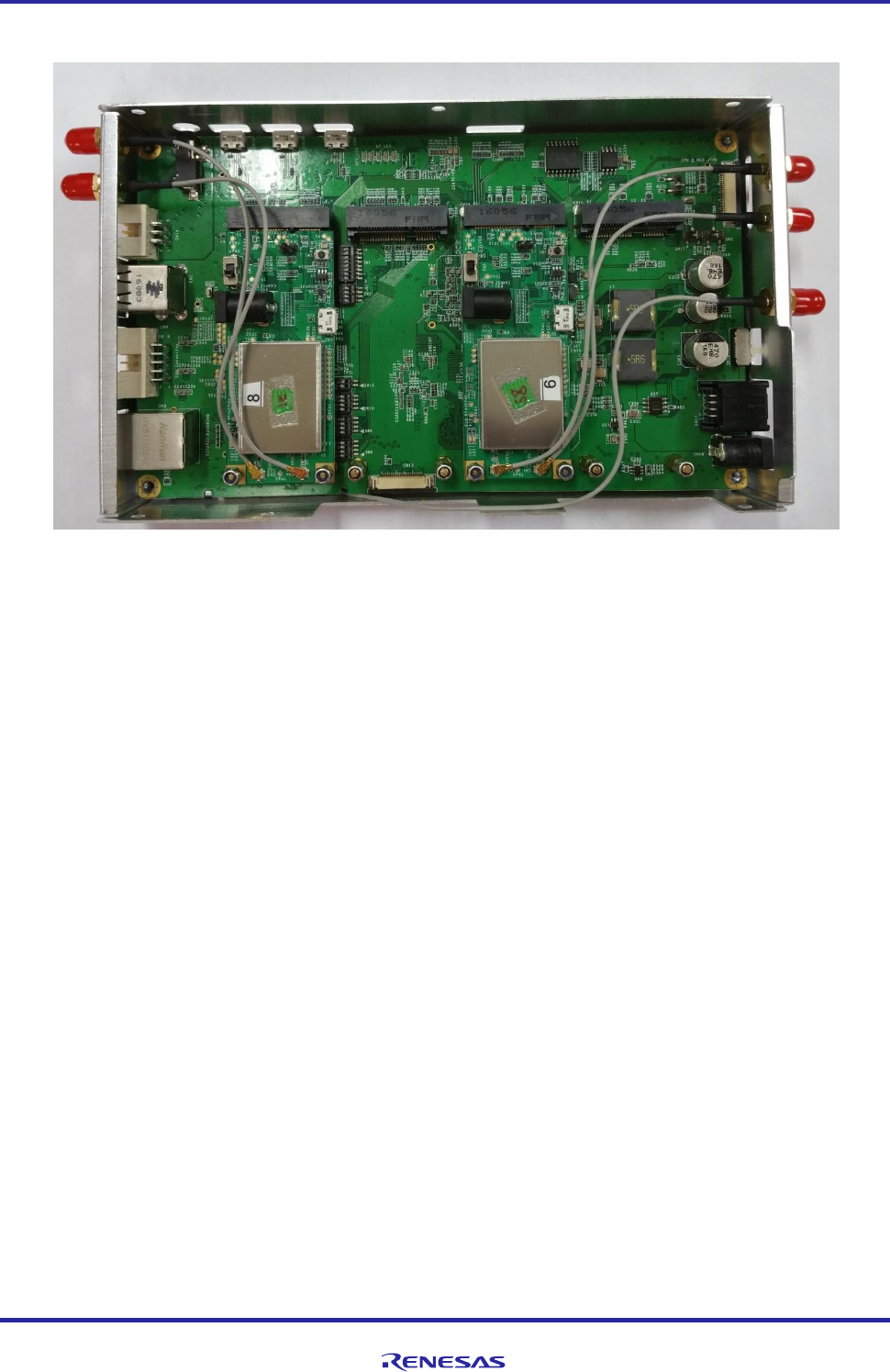
Hardware Design Specification
ASD-B-16-0247 Rev1.3 Page
66
of 105
September 8, 2017
RTK00V2XRC7746SFS
V2X RF Cable/GPS RF Cable connection image internal AL case
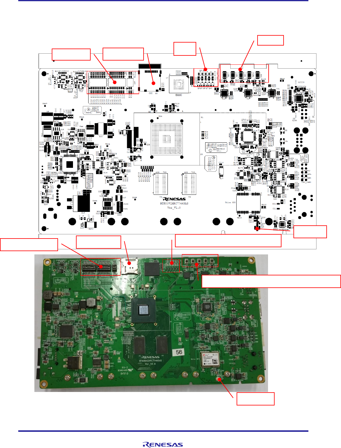
Hardware Design Specification
ASD-B-16-0247 Rev1.3 Page
67
of 105
September 8, 2017
RTK00V2XRC7746SFS
6 Board connectors
6.1 TOP side connectors
The top side connector is shown as the picture in the following.
Figure 25 TOP Side Connectors
SD Card CN2
GPS CN7
SD Card CN
GPS CN
DIP Switch
Switch
LED
SW5、SW6、SW7
D9、D7、D5、D3、D11 (GPS_LED)
SW16、SW15、SW14、SW13、(SW4) MCU reset
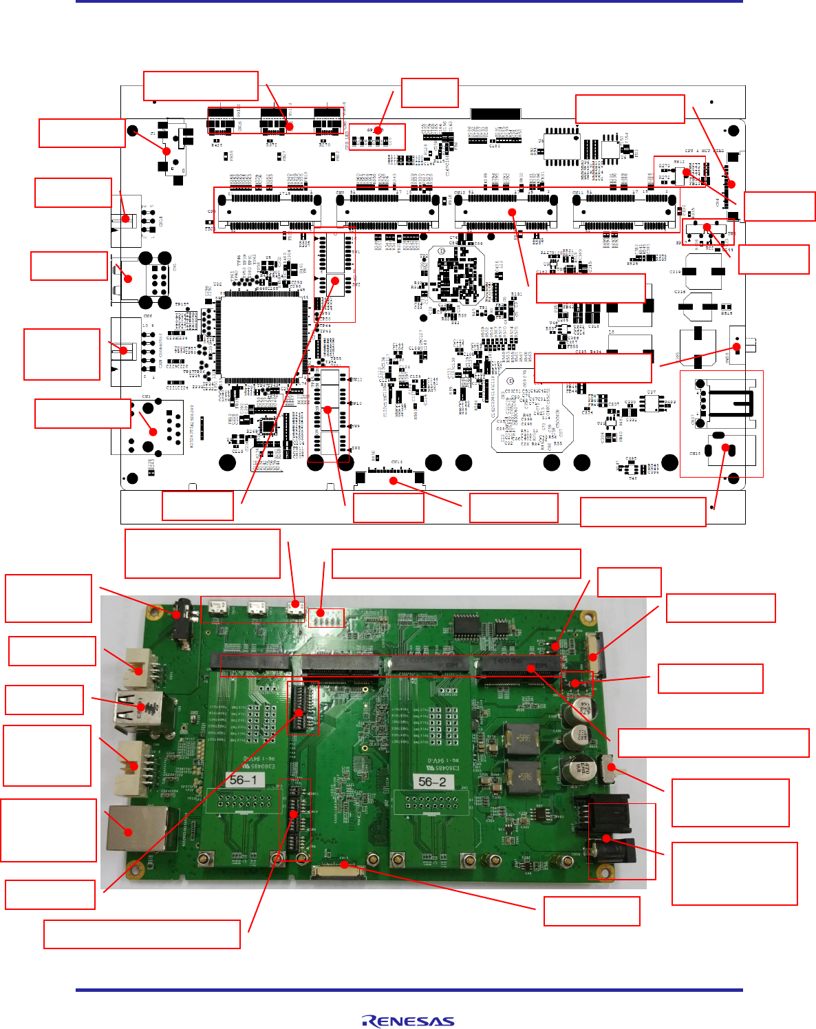
Hardware Design Specification
ASD-B-16-0247 Rev1.3 Page
68
of 105
September 8, 2017
RTK00V2XRC7746SFS
6.2 Bottom side connectors
The bottom side connectors are shown as the picture in the following.
Figure 26 Bottom side connectors
HSM CN
CAN&Fle
xray CN
Ethernet CN
Audio jack
USB CN
Micro USB
CN16、CN10、CN5
POWER Switch
SW18
POWER IN JACK
CN17 and CN18
ETNB CN13
MINI PCIE CN
DEBUG CN
DEBUG CN14
HSM CN14
CAN&Flexr
ay CN6
Ethernet
CN3
Audio jack
J1
USB CN1
CN9、CN8、CN12、CN11
POWER Switch
POWER IN JACK
ETNB CN
DIP SW
DIP SW
DIP SW
Micro USB CN
LED
DIP SW
D12 (GPS_LED)、D4、D6、D8、D10
SW12
SW17、SW3
SW1、SW2
SW11、SW10、SW9、SW8
Hardware Design Specification
ASD-B-16-0247 Rev1.3 Page
69
of 105
September 8, 2017
RTK00V2XRC7746SFS
6.3 The details of connectors
(1) There are two USB connectors, the CN1B is corresponding to Tethys from HUB and CN1A is
corresponding to Tethys from W2H respectively as the picture shown above.
(2) The CAN pin assignments are shown as below:
CN6 PIN Number
Signal
Remark
1
CPU_CAN0_H
HIGH-level CAN bus line
2
CPU_CAN0_L
LOW-level CAN bus line
3
MCU_CAN0_H
HIGH-level CAN bus line
4
MCU_CAN0_L
LOW-level CAN bus line
5
MCU_CAN1_H
HIGH-level CAN bus line
6
MCU_CAN1_L
LOW-level CAN bus line
7
BP
Flexray bus line plus
8
BM
Flexray bus line minus
9
GND
Ground
10
GND
Ground
As the picture shown above, there are there USB2UART connectors from the left to right as the figure
shown, they are for MCU debug, sub board V2X debug and CPU debug respectively.
MCU Debug
CPU Debug
Sub Board V2X
Debug
CH2 & CH3 GPS:
to V2X SUB(CN12) to Tethys CN7
2 4 6 8 10
1 3 5 7 9
CN1B: USB1
CN1A:USB0
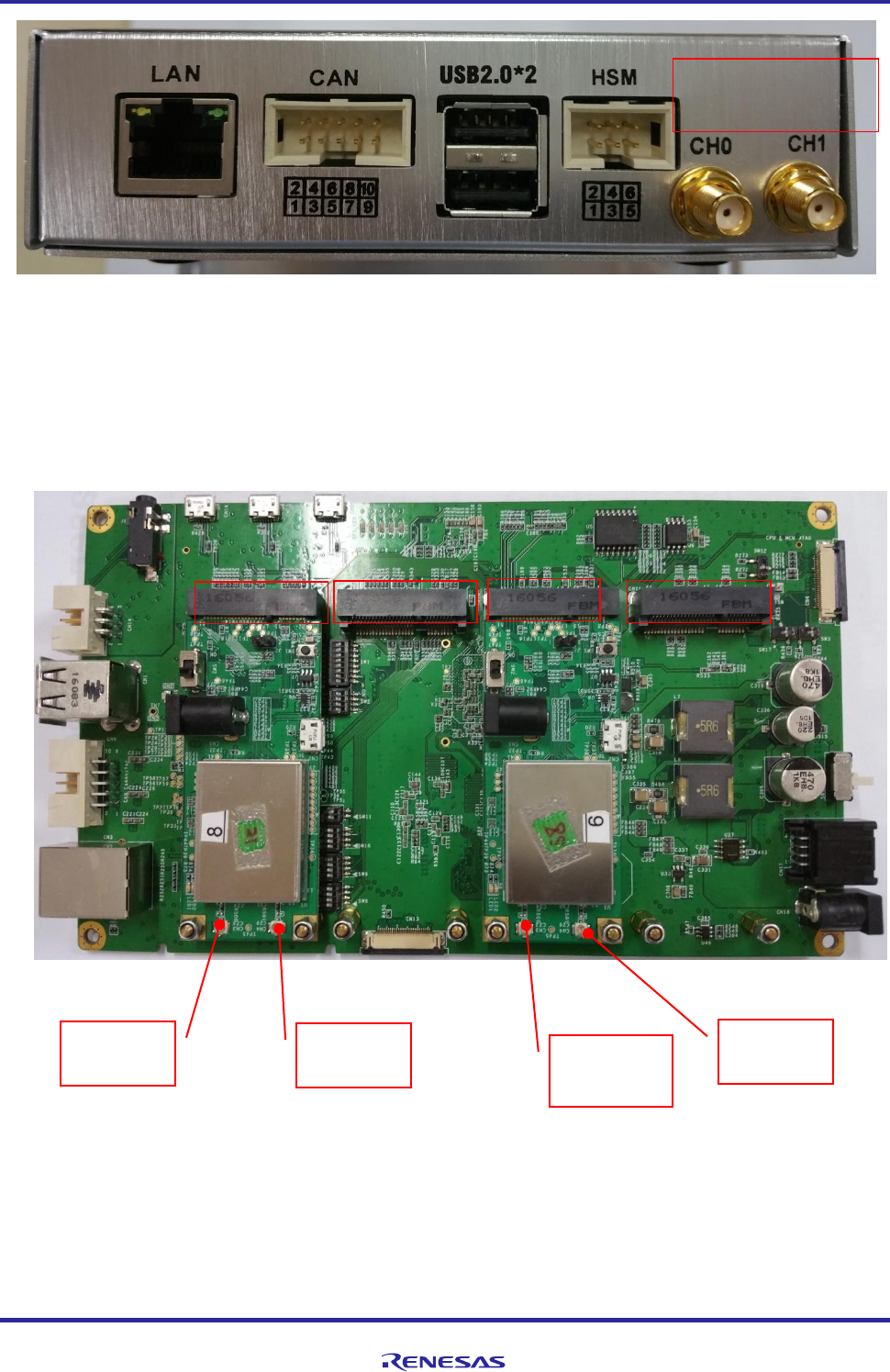
Hardware Design Specification
ASD-B-16-0247 Rev1.3 Page
70
of 105
September 8, 2017
RTK00V2XRC7746SFS
As the picture shown above, there are five RF connectors to the antenna. In the inner connection, the CH2 and
CH3 are for the V2X sub-board which is inserted in Tethys MINI PCIE connector CN12, the CH0 and CH1 are
for the V2X sub-board which is inserted in the Tethys MINI PCIE connector CN9. The GPS is for Tethys GPS
module antenna connector CN7 at the top side.
One possible connection is shown as the picture in the following picture:
CH0 & CH1
to V2X SUB (CN9)
CN12
CN8
CN9
Connect to
CH0
Connect to
CH1
Connect to
CH2
Connect to
CH3
CN11
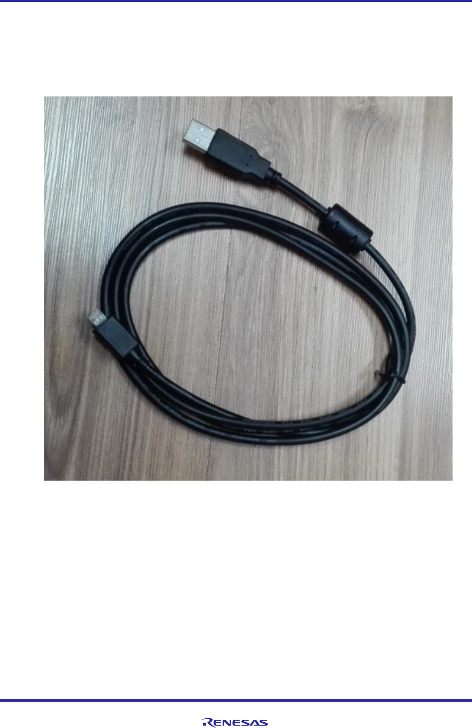
Hardware Design Specification
ASD-B-16-0247 Rev1.3 Page
71
of 105
September 8, 2017
RTK00V2XRC7746SFS
7 Appendix
7.1 USB debug Cable
USB debug Cable Length:1.5m, This USB cable is used for Micro USB type B connector CN5, CN10, CN16 for debug
on V2X main board. This cable can be inserted to miniUSB1/miniUSB2/miniUSB3 connector.
Figure 27 Image of USB debug cable
Hardware Design Specification
ASD-B-16-0247 Rev1.3 Page
72
of 105
September 8, 2017
RTK00V2XRC7746SFS
7.2 AC Adapter
This 12V AC adapter is used for power supply to the Tethys.
7.2.1 Specifications
Item
Specification
Part Number
GPE048A-120300-W
Manufacturer
GOLDEN PROFIT ELECTRONICS LTD
Input voltage range
90-264V AC
Input frequency range
63/47 Hz
AC input current
1A Max .@100V AC
AC input power saving
0.075W Max .@230V AC at no load
Inrush Current
60 A Max .@100VAC (Cold start)
90 A Max .@230VAC (Cold start)
Leakage current
0.25mA Max
Output voltage
12V
Max. load current
3A
Min. load current
0A
Output voltage
12 V± 5%
Output ripple & noise
12 V± 5%
Total output power
36 W
Operating Temp
0~40℃
Storage Temp
–25℃ to 85℃
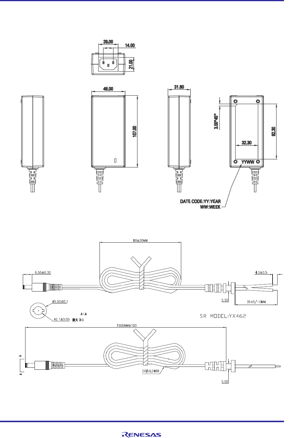
Hardware Design Specification
ASD-B-16-0247 Rev1.3 Page
73
of 105
September 8, 2017
RTK00V2XRC7746SFS
7.2.2 Mechanic Size and Picture
Mechanic Size:
Cable Spec:
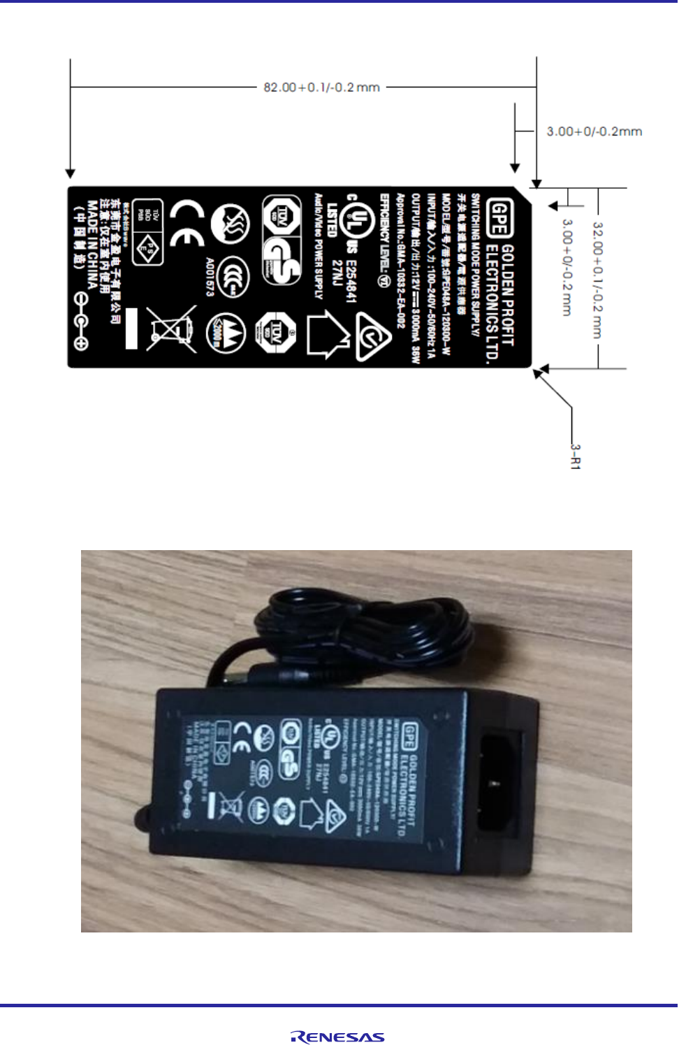
Hardware Design Specification
ASD-B-16-0247 Rev1.3 Page
74
of 105
September 8, 2017
RTK00V2XRC7746SFS
LOG Image:
Figure 28 Power Adapter ID LOG specification
Figure 29 Image of Power Adapter
Hardware Design Specification
ASD-B-16-0247 Rev1.3 Page
75
of 105
September 8, 2017
RTK00V2XRC7746SFS
7.3 GPS antenna
7.3.1 Specification
About GPS antenna specification, please refer to the following data:
Table 27 Antenna Specification for GPS module
Item
Specification
Part Number
DAM1575 A4D1
Manufacturer
Taiwan ACC
Cable Length
5m
Center Frequency
1575MHz ± 3MHz
VSWR
Maximum 2.0
Bandwidth
Minimum 20MHz
IF Resister
50ohm
Peak Gain
4 dBic(base on 70mm x 70mm ground plane)
Gain coverage
≥-4dBic at -90°<θ<+90°(over 75% volume)
Polarity
RHCP
Power consumption
1 watt
Gain
30dB(typical)
Noise parameter
1.5dB(typical)
Material
Copper
Plating treatment
Gold plating
Male/Female
Male
Filter
-24dB(±100mHz)
DC voltage
3-5.0V ±0.25V
DC current
Maximum 16mA
Weight
≤110 g
Size
50x50x17 mm3
Cable type
rg174, 5m
IF Type
SMA
Color
Black
Work temperature
-40℃~ +85℃
Save temperature
-40℃~ +85℃
Vibration
sine wave, 1g(0-p) 10-150-10Hz for each axis
Humidity
95%~100%, no condensation
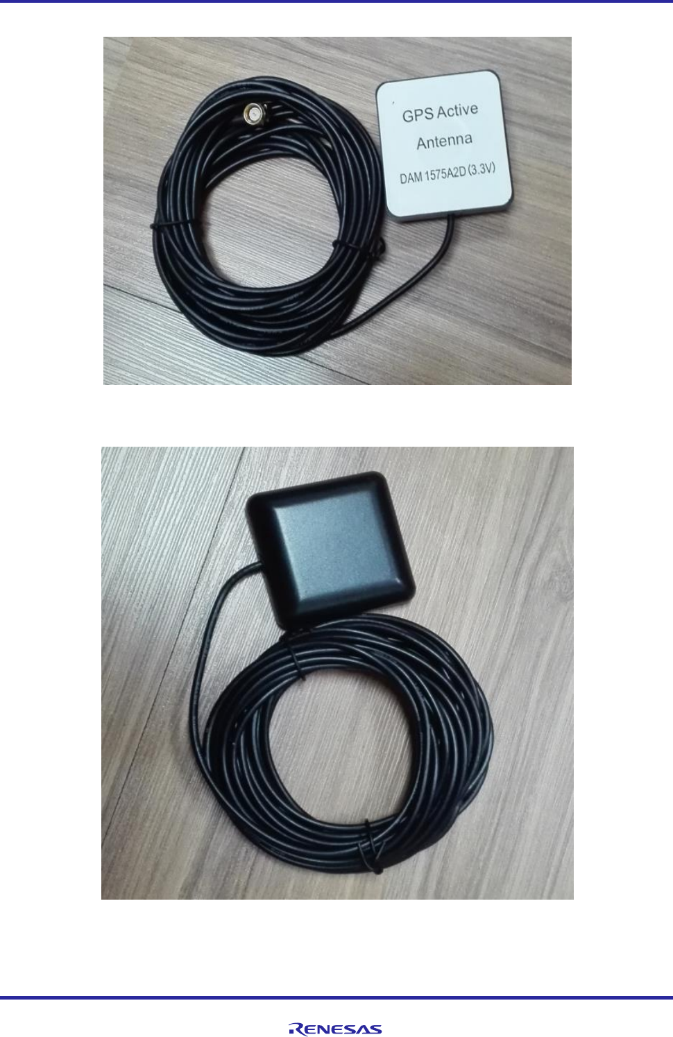
Hardware Design Specification
ASD-B-16-0247 Rev1.3 Page
76
of 105
September 8, 2017
RTK00V2XRC7746SFS
This GPS antenna connect the SMA connector labeled GPS in the case. Cable Length: 5m
Figure 30 Image of GPS Antenna from Bottom view
Figure 31 Image of GPS Antenna from Top view
Hardware Design Specification
ASD-B-16-0247 Rev1.3 Page
77
of 105
September 8, 2017
RTK00V2XRC7746SFS
7.4 V2X Antenna1 with 2m cable
7.4.1 Specification
About V2X antenna specification, please refer to the following data:
Table 28 Antenna Specification for V2X (2m cable)
Item
Specification
Part Number
6073F00005
Manufacturer
Signal Plus
Frequency Range
5860~ 5920MHz
Polarization
Horizontal
Impedance
50 Ohm
VSWR
2.0 Max
Gain
3.0dBi(without cable loss)
-1.0dBi(with cable loss)
Cable Loss
4.0dB(L=2m)
Radiation
Omni Directional
Cable length
2m
Antenna Cap
ABS
Color
Black
Connector
SMA Plug Standard
Material
Copper
Plating treatment
Gold plating
Male/Female
Male
Operating Temp
-20℃ ~ +65℃
Storage Temp
-30℃ ~ +75℃
Hardware Design Specification
ASD-B-16-0247 Rev1.3 Page
78
of 105
September 8, 2017
RTK00V2XRC7746SFS
This Antenna’s radiation pattern is described as below figures.
Figure 32 V2X Antenna Test Chamber description
Hardware Design Specification
ASD-B-16-0247 Rev1.3 Page
79
of 105
September 8, 2017
RTK00V2XRC7746SFS
Figure 33 V2X Antennal test axis definition description
Hardware Design Specification
ASD-B-16-0247 Rev1.3 Page
80
of 105
September 8, 2017
RTK00V2XRC7746SFS
Figure 34 V2X Antennal VSWR test character
Hardware Design Specification
ASD-B-16-0247 Rev1.3 Page
81
of 105
September 8, 2017
RTK00V2XRC7746SFS
Figure 35 V2X Antennal 2D radiation pattern
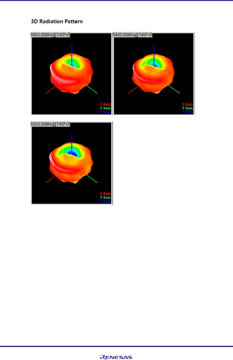
Hardware Design Specification
ASD-B-16-0247 Rev1.3 Page
82
of 105
September 8, 2017
RTK00V2XRC7746SFS
Figure 36 V2X Antennal 3D radiation pattern
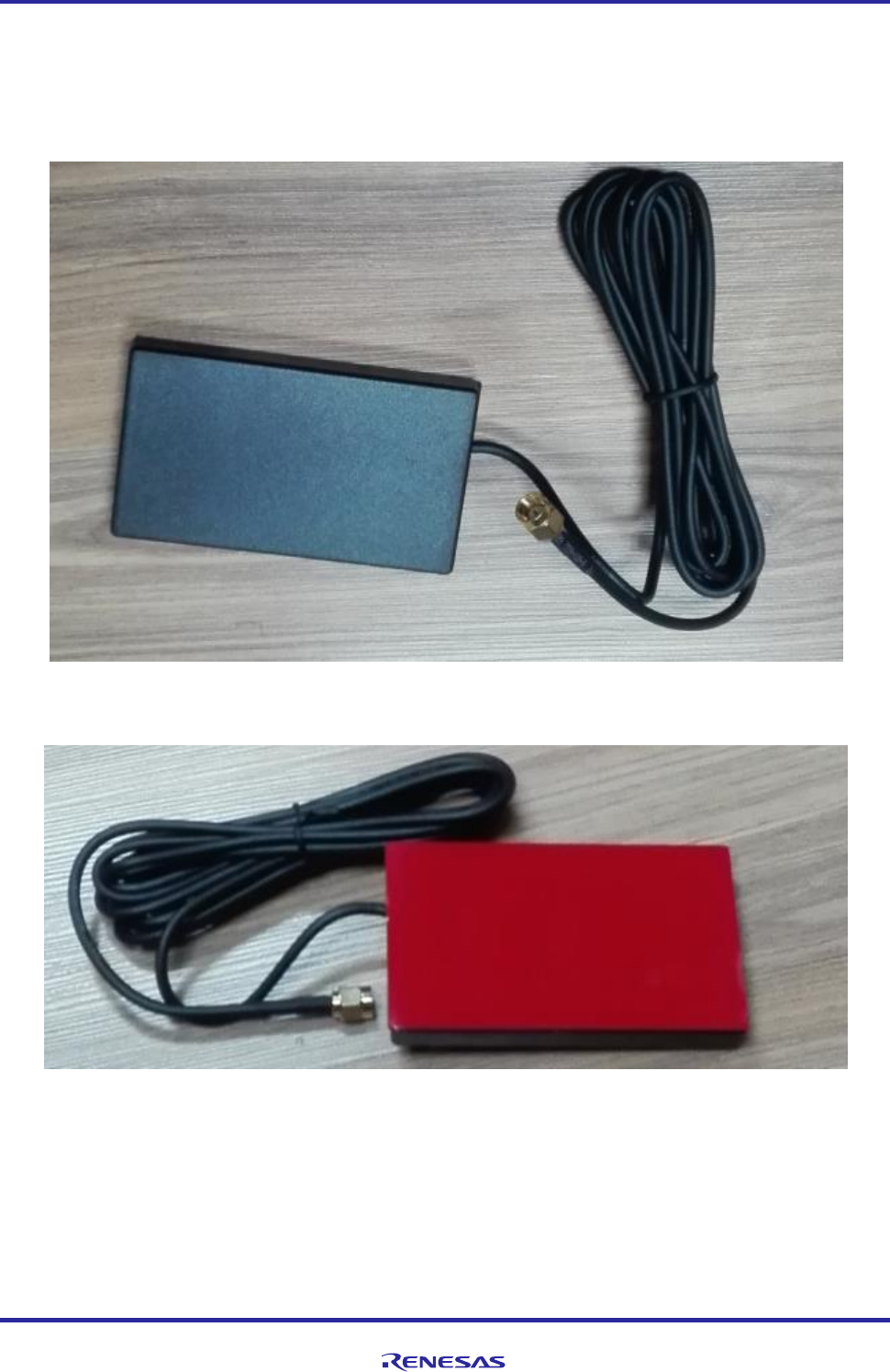
Hardware Design Specification
ASD-B-16-0247 Rev1.3 Page
83
of 105
September 8, 2017
RTK00V2XRC7746SFS
This V2X antenna connects with the SMA connector labeled CH0, CH1, CH2, CH3 in the case by default while
delivery.
Cable Length: 2m
Figure 37 Image of V2X Antenna1 from Bottom view
Figure 38 Image of V2X Antenna1 from Top view
Hardware Design Specification
ASD-B-16-0247 Rev1.3 Page
84
of 105
September 8, 2017
RTK00V2XRC7746SFS
7.5 V2X Antenna (Rod Type)
7.5.1 Specification
About 5.9GHz V2X antenna specification, please refer to the following data:
Table 29 Antenna Specification for V2X (Rod Type)
Item
Specification
Part Number
6073F00006
Manufacturer
Signal Plus
Frequency Range
5860~ 5920MHz
Polarization
Vertical
Impedance
50 Ohm
VSWR
2.0 Max
Gain
5.0dBi
Cable Loss
0.5dB (with SMA)
Radiation
Omni Directional
Color
Black
Connector
SMA Plug Standard
Material
nickel
Plating treatment
nickel plating
Male/Female
Male
Operating Temp
-20℃ ~ +65℃
Storage Temp
-30℃ ~ +75℃
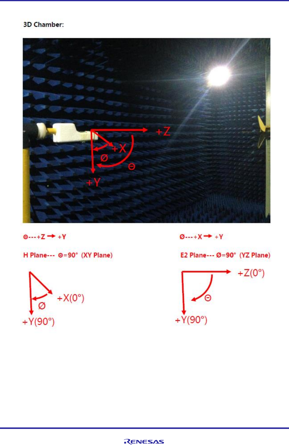
Hardware Design Specification
ASD-B-16-0247 Rev1.3 Page
85
of 105
September 8, 2017
RTK00V2XRC7746SFS
This Antenna’s radiation pattern is described as below figures.
Figure 39 V2X Antenna2 Test Chamber description
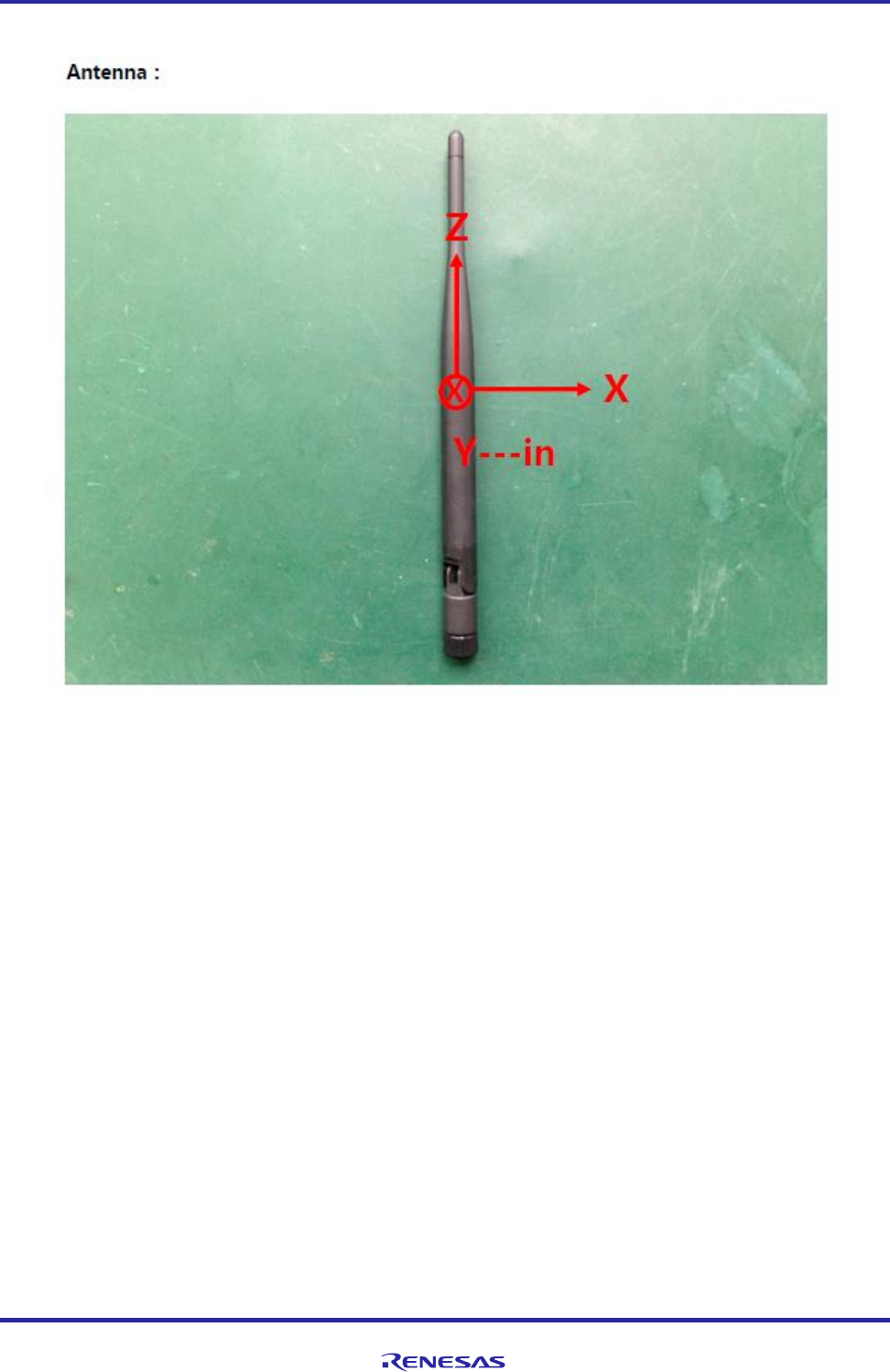
Hardware Design Specification
ASD-B-16-0247 Rev1.3 Page
86
of 105
September 8, 2017
RTK00V2XRC7746SFS
Figure 40 V2X Antenna2 test axis definition description
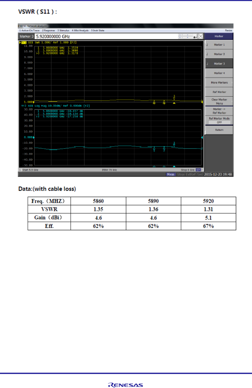
Hardware Design Specification
ASD-B-16-0247 Rev1.3 Page
87
of 105
September 8, 2017
RTK00V2XRC7746SFS
Figure 41 V2X Antenna2 VSWR test character
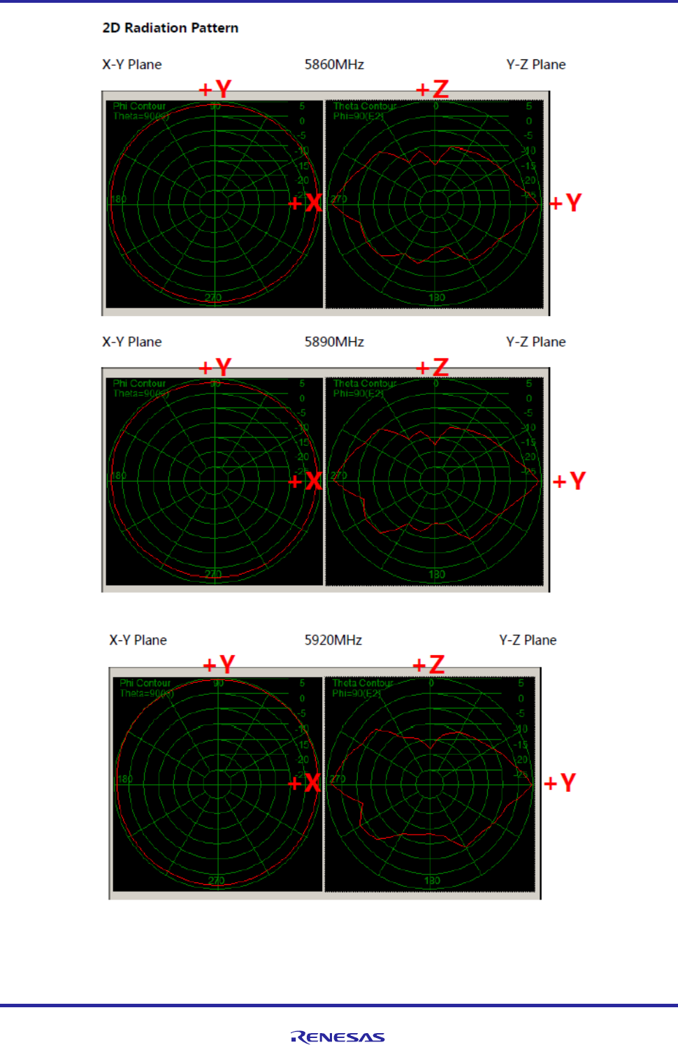
Hardware Design Specification
ASD-B-16-0247 Rev1.3 Page
88
of 105
September 8, 2017
RTK00V2XRC7746SFS
Figure 42 V2X Antenna2 2D radiation pattern
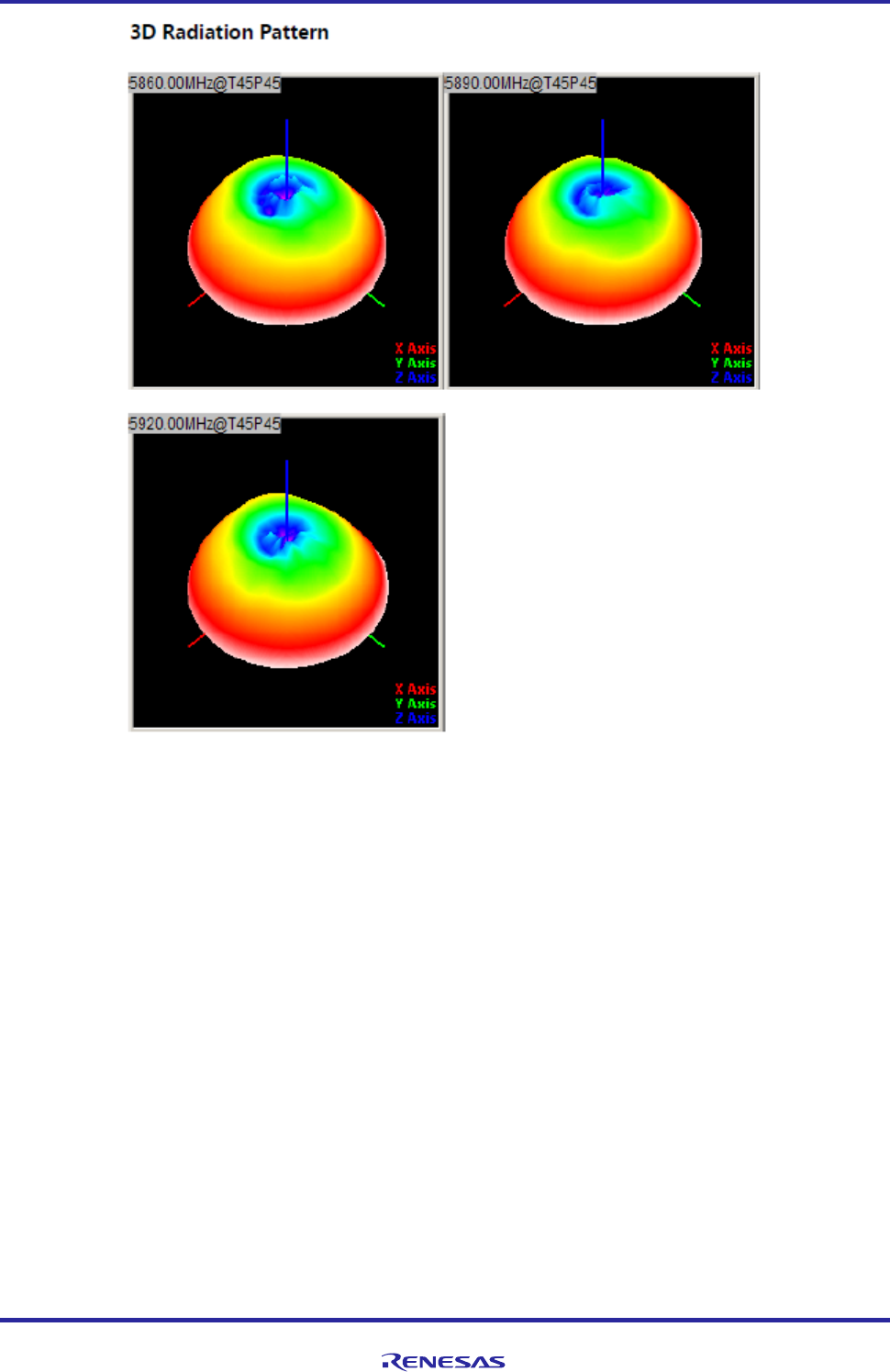
Hardware Design Specification
ASD-B-16-0247 Rev1.3 Page
89
of 105
September 8, 2017
RTK00V2XRC7746SFS
Figure 43 V2X Antenna2 3D radiation pattern

Hardware Design Specification
ASD-B-16-0247 Rev1.3 Page
90
of 105
September 8, 2017
RTK00V2XRC7746SFS
Figure 44 Image of V2X Antenna2 (SMA rotate 90 degree)
Figure 45 Image of V2X Antenna2 (SMA rotate 0 degree)
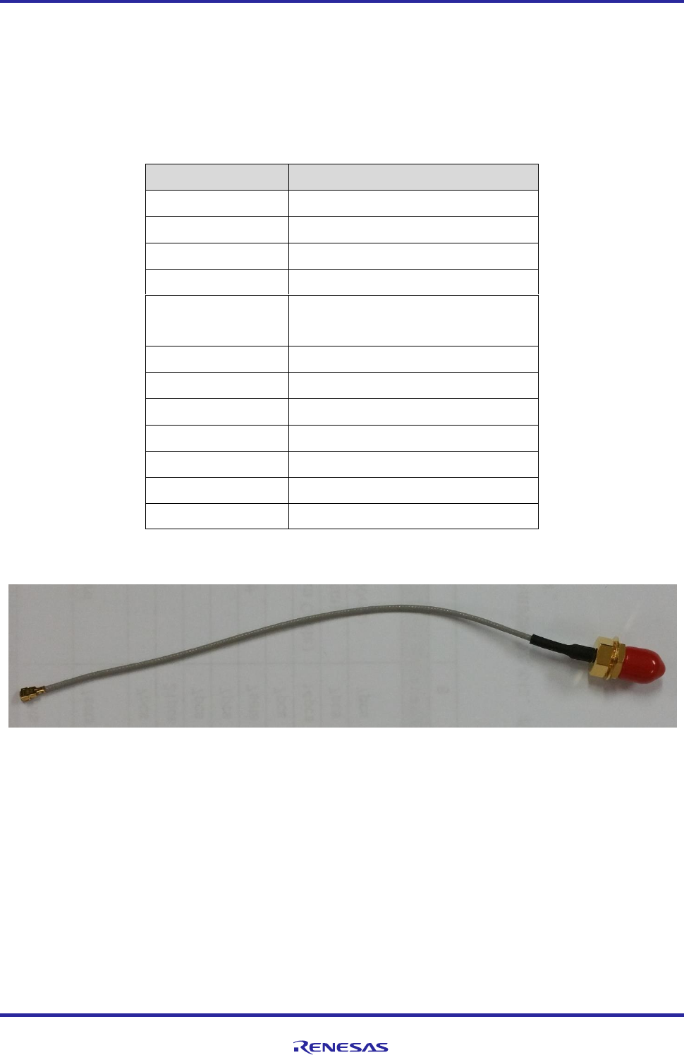
Hardware Design Specification
ASD-B-16-0247 Rev1.3 Page
91
of 105
September 8, 2017
RTK00V2XRC7746SFS
7.6 RF Cable
7.6.1 Specification
About RF Cable specification, please refer to the following data:
Table 30 RF Cable Specification for GPS module & RF Board
Item
Specification
Frequency Range
0~ 6GHz
Impedance
50 Ohm
VSWR
1.4 Max
Cable Loss
1.3dB Max
Cable length
(1)13~15cm for V2X
(2)20cm for GPS
Cable Type
U.FL-LP-088
Connector
SMA
Material
Copper
Plating treatment
Gold plating
Male/Female
Female
Operating Temp
-40℃ ~ +90℃
Storage Temp
-40℃ ~ +70℃
Figure 46 RF Cable
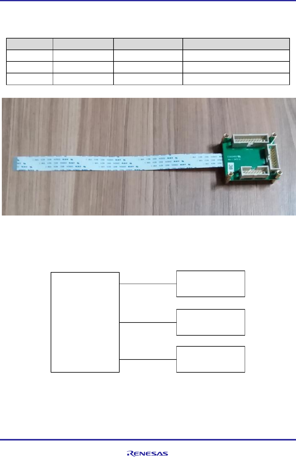
Hardware Design Specification
ASD-B-16-0247 Rev1.3 Page
92
of 105
September 8, 2017
RTK00V2XRC7746SFS
7.7 JTAG Debug Board with FPC Cable
7.7.1 Specifications
Connecter
Function
Debugger
Manufacturer
CN1
CPU JTAG
ARM JTAG ICE Debugger
ARM JTAG ICE Vendor
CN4
CPU JTAG2(SH-4AL)
E10A
Renesas (Japan)
CN3
MCU JTAG
E1
Renesas (Japan)
Figure 47 JTAG Debug Board with FPC Cable for R-CAR W2H & RH850 MCU
7.7.2 Block Structure
CONN(2)
CPU JTAG ( 02 )
CPU JTAG2 ( SH-4AL )
( 02 )
MCU JTAG ( 02 )
Figure 48 JTAG Debug Board block structure
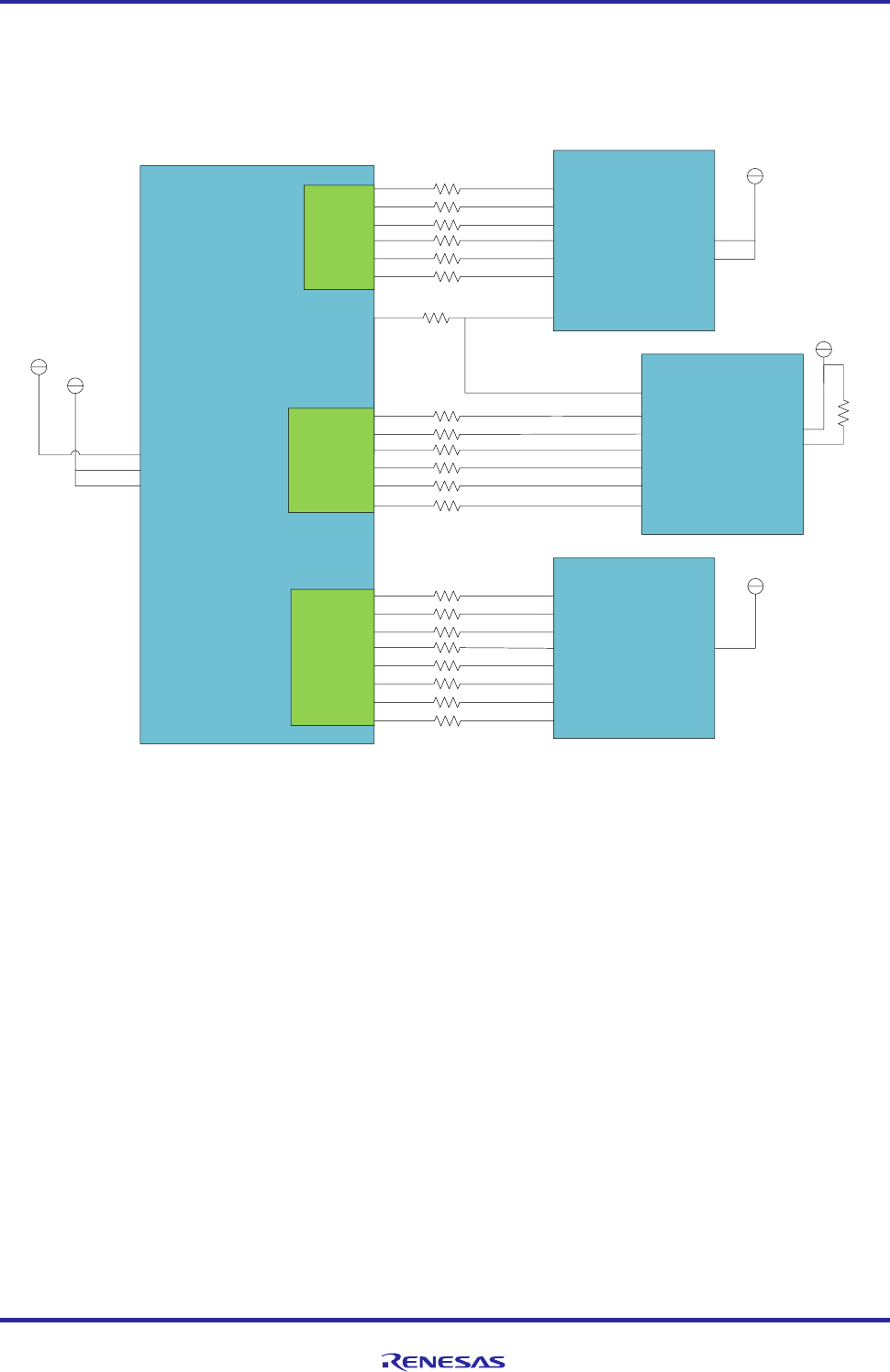
Hardware Design Specification
ASD-B-16-0247 Rev1.3 Page
93
of 105
September 8, 2017
RTK00V2XRC7746SFS
7.7.3 Block Diagram
TRSTn
TDI
TMS
TCK
TDO
SYS_RESETn_18
ASEBRKn
TRST
TDI
TMS
TDO
TCK
SRSTZ
NC1
HTST-110-01-S-DV
CN1
0
0
0
0
0
0
0
CPU
JTAG
MMC0_CMD_TRST
MMC0_D2_TDI
MMC0_D1_TMS
MMC0_D0_TCK
MMC0_D3_ASEBRK#/ACK
21
1-1634688-4
CN4
0
0
0
0
0
CPU
JTAG2
(SH-4AL) MMC0_CLK_TDO
0
SYS_RESETn_18 13
3
11
9
1
5
7
DCUTRST
DCUTDI
DCUTMS
DCUTCK
DCUTDO
MCU_RESETn
0
0
0
0
0
0
MCU
JTAG
1-1634688-4
CN4
0
0
DCURDY
FLMD0
3
7
9
1
5
13
11
4
IMSA-9632S-26Y801
CN2
D1.8V
D1.8V
BU3.3V
BU3.3V
D1.8V
26
25
24
23
22
20
6
5
4
3
2
1
19
18
17
16
15
14
13
12
VDD0
VDD1
8
9
8
7
4.7K
4
8
Figure 49 Block Diagram of the JTAG Debug Board
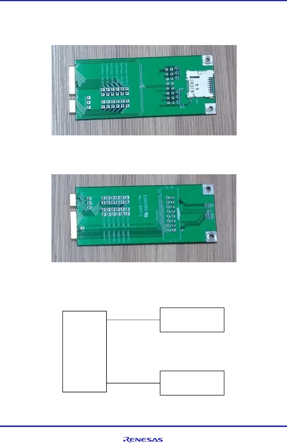
Hardware Design Specification
ASD-B-16-0247 Rev1.3 Page
94
of 105
September 8, 2017
RTK00V2XRC7746SFS
7.8 V2X Connection board
This sub board can be connected to CN9 or CN12 to extend SD socket IF.
Top side view:
Figure 50 Top side view of V2X Connection board
Bottom side view:
Figure 51 Bottom side view of V2X Connection board
7.8.1 Board Structure
GOLD finger ( 2 )
CONN ( 02 )
Micro SD SLOT ( 02 )
Figure 52 Block structure of V2X Connection board
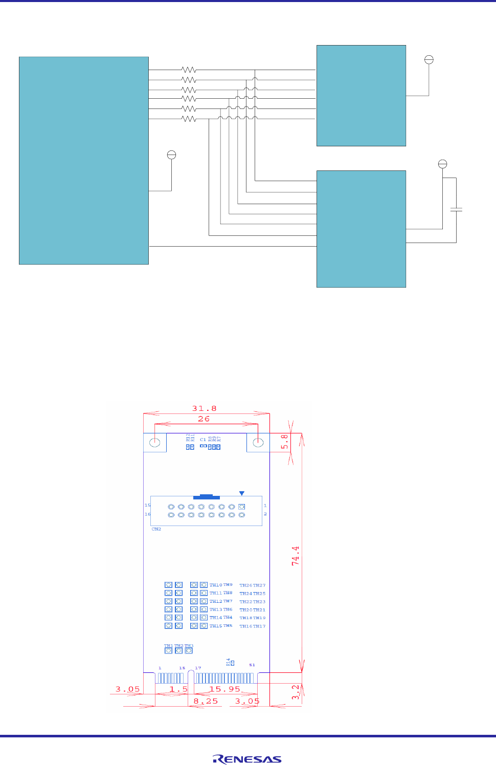
Hardware Design Specification
ASD-B-16-0247 Rev1.3 Page
95
of 105
September 8, 2017
RTK00V2XRC7746SFS
7.8.2 Block Diagram
Connect to C2X
HTST-108-01-F-D
CN2
33
33
33
33
33
0
Mini PCIE
PLUG
Gold finger
CN1
D3.3V
D3.3V
RESERVED6 SDIO_DAT2
SDIO_DAT1
SDIO_DAT0
SDIO_CMD
SDIO_CLK
SDIO_DAT3
SDIO_DAT3
SDIO_DAT2
SDIO_DAT1
SDIO_DAT0
SDIO_CMD
SDIO_CLK
RESERVED7
RESERVED8
RESERVED9
RESERVED10
RESERVED3
CD/DAT3
DAT2
DAT1
DAT0
CMD
CLK
3
1
15
13
5
11
Micro SD slot
503182-1852
CN3
RESERVED4 SD_CD PAD
VDD
PAD
100nF/25V
9
3.3V
D3.3V
Figure 53 Block Diagram of the V2X Connection board
7.8.3 Block dimension
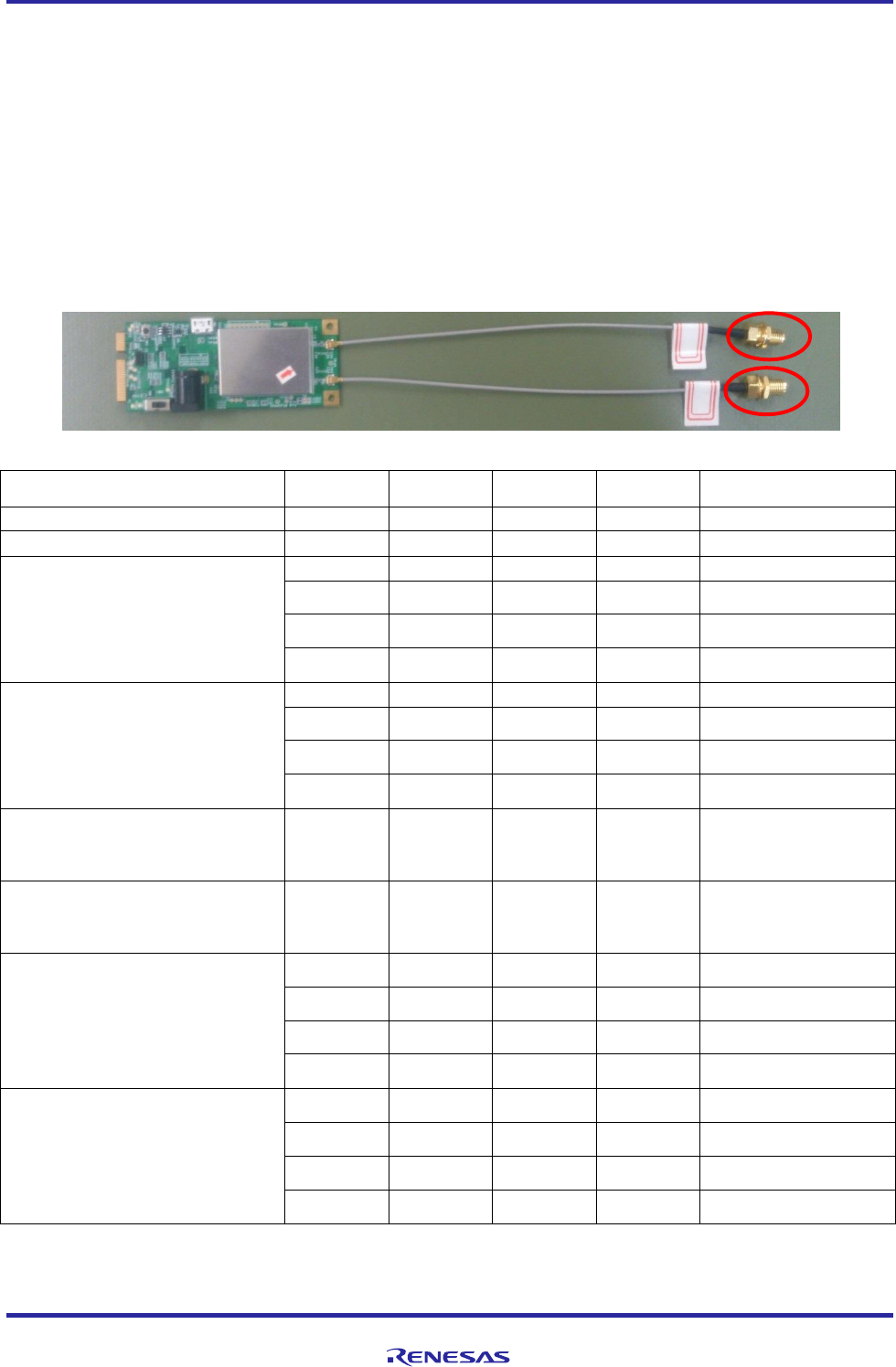
Hardware Design Specification
ASD-B-16-0247 Rev1.3 Page
96
of 105
September 8, 2017
RTK00V2XRC7746SFS
7.9 Sub board Tortuga wireless module board dimension
The Tethys board can connect to Tortuga wireless module through MINI PCIE interface transfer board, and the transfer
sub board dimension is shown as below(Unit: mm): Please connect this board to CN9, CN12.
7.9.1 RF characteristic
*1 typical operating condition (Just informative, not guaranteed.):
*1 HW = Tortuga7, Ta = 25°C, VDD3V3 =3.3V, VDD1V2 =1.2V, VDD5V0=5.0V
*1 Measurement point is circled in red in the figure below
(1) Receive characteristic
Min
Typ
Max
Unit
Condition
Frequency range
5850
5925
[MHz]
Input VSWR
2.0
-
5890MHz
Minimum Sensitivity
(Diversity off)
-94
[dBm]
Data rate = 3Mbps
-93
[dBm]
Data rate = 6Mbps
-87
[dBm]
Data rate = 12Mbps
-77
[dBm]
Data rate = 27Mbps
Minimum Sensitivity
(Diversity on)
-94
[dBm]
Data rate = 3Mbps
-94
[dBm]
Data rate = 6Mbps
-87
[dBm]
Data rate = 12Mbps
-80
[dBm]
Data rate = 27Mbps
Maximum
Input Level
(Diversity off)
-20
[dBm]
Data rate = 27Mbps
Maximum
Input Level
(Diversity on)
-20
[dBm]
Data rate = 27Mbps
Adjacent channel rejection
(Diversity off)
30
[dB]
Data rate = 3Mbps
29
[dB]
Data rate = 6Mbps
28
[dB]
Data rate = 12Mbps
18
[dB]
Data rate = 27Mbps
Nonadjacent Adjacent channel
rejection
(Diversity off)
44
[dB]
Data rate = 3Mbps
41
[dB]
Data rate = 6Mbps
36
[dB]
Data rate = 12Mbps
27
[dB]
Data rate = 27Mbps
(2) Transmit characteristic
Hardware Design Specification
ASD-B-16-0247 Rev1.3 Page
97
of 105
September 8, 2017
RTK00V2XRC7746SFS
Ta = 25°C, VDD3V3 =3.3V, VDD1V2 =1.2V, VDD5V0=5.0V
Min
Typ
Max
Unit
Condition
Frequency range
5850
5925
[MHz]
Output VSWR
2.0
5890MHz
Maximum out put
Power(ANT_B)
24
[dBm]
5890MHz
Maximum out put
Power(ANT_A)
-8
[dBm]
5890MHz
Minimum out put Power(ANT_B)
-7
[dBm]
5890MHz
Minimum out put Power(ANT_A)
-35
[dBm]
5890MHz
Output Power control range
30
[dB]
5890MHz
Power control step
0.5
[dB]
Relative constellation error
-28
[dB]
Data rate = 3Mbps
-28
Data rate = 6Mbps
-28
Data rate = 12Mbps
-28
Data rate = 27Mbps
Spectrum Mask
(in band)
-31
[dBr/100
KHz]
@5890
MHz
4.5MHz<f<5.0MHz offset
Pout = 24dBm
-33
5.0MHz<f<5.5MHz offset
Pout =24dBm
-36
5.5MHz<f<10.0MHz offset
±5.5MHz Pout=
24dBm
-54
10.0MHz<f<15.0MHz offset
Pout=24dBm
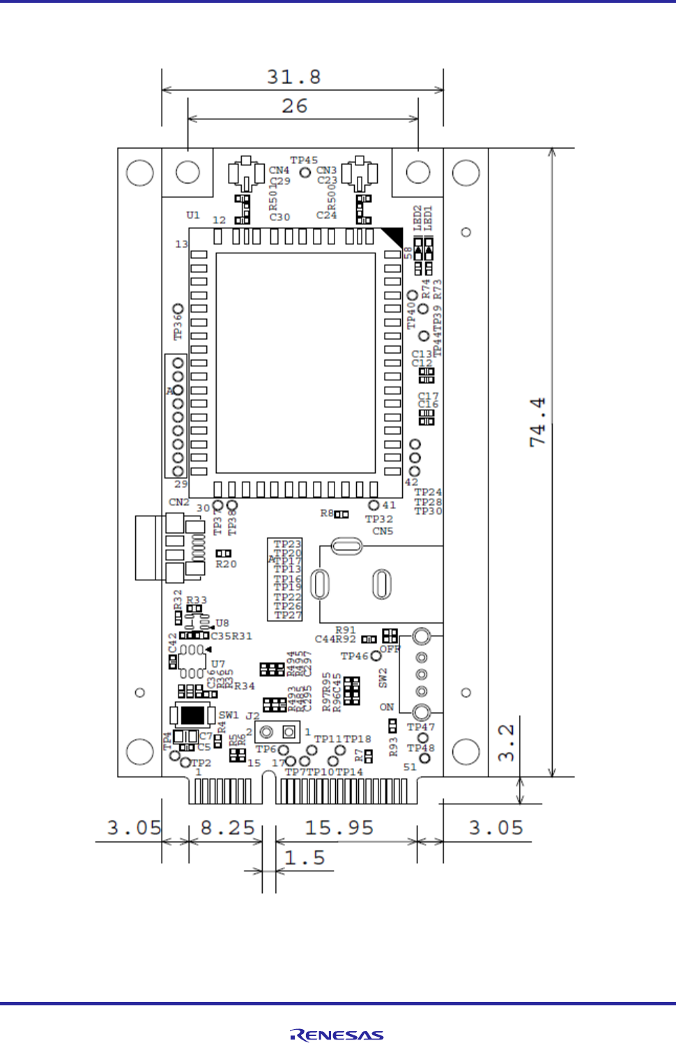
Hardware Design Specification
ASD-B-16-0247 Rev1.3 Page
98
of 105
September 8, 2017
RTK00V2XRC7746SFS
7.9.2 Board Dimension
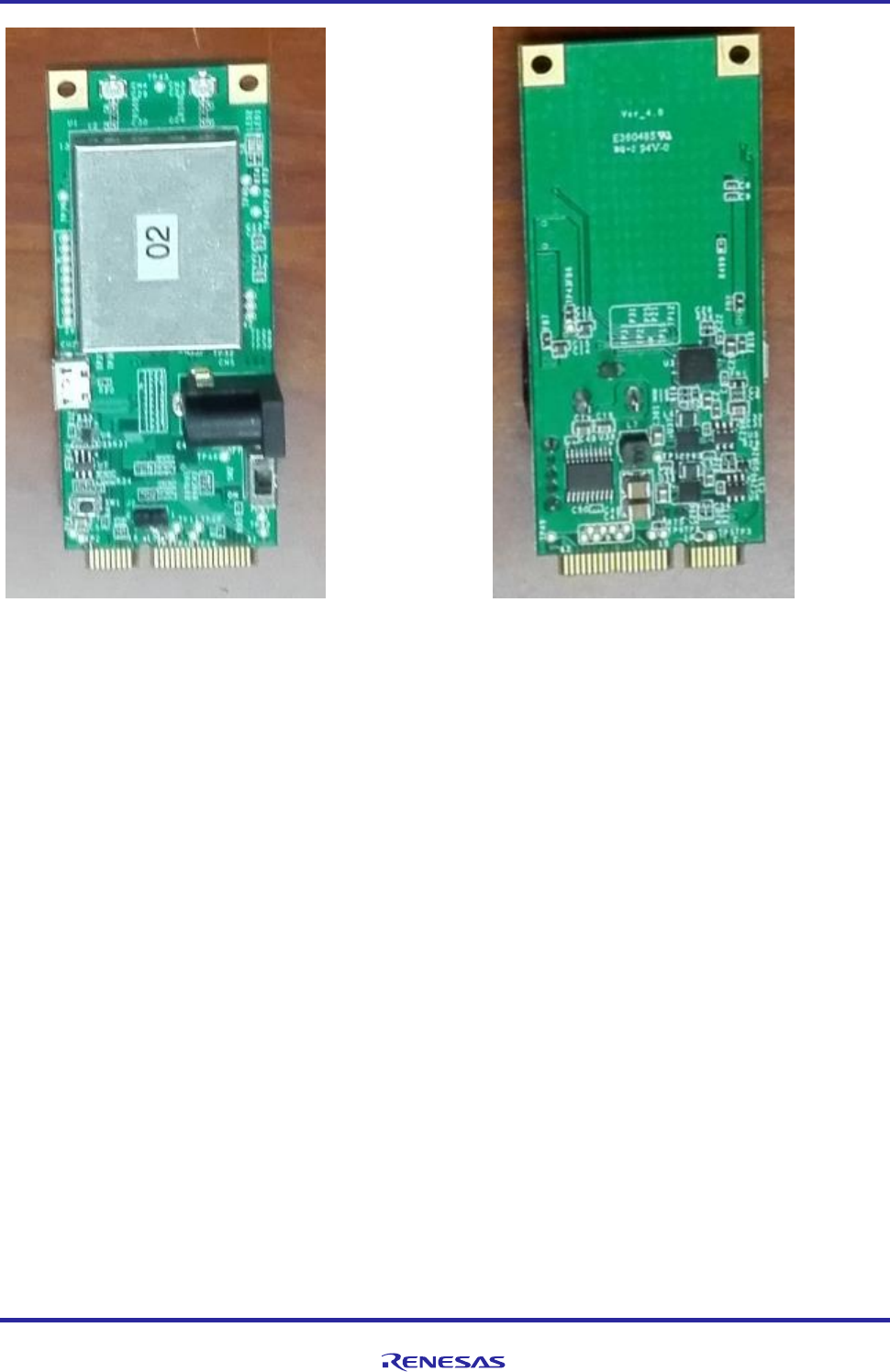
Hardware Design Specification
ASD-B-16-0247 Rev1.3 Page
99
of 105
September 8, 2017
RTK00V2XRC7746SFS
Top Side Bottom Side
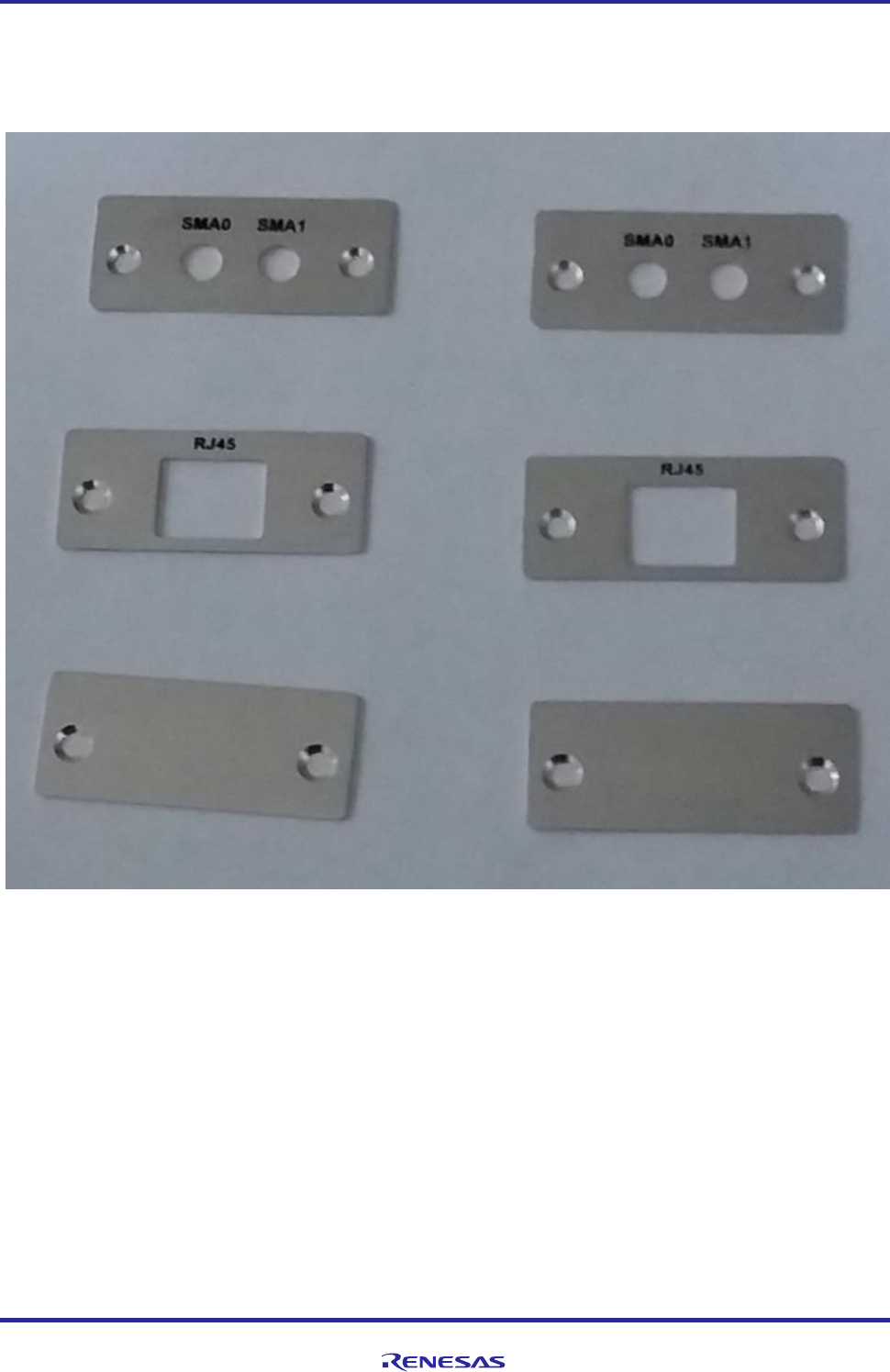
Hardware Design Specification
ASD-B-16-0247 Rev1.3 Page
100
of 105
September 8, 2017
RTK00V2XRC7746SFS
7.10 Side cover option of case
AL Case includes the following 2 sets of side cover option which will be used depending on the sub board type, which
is inserted in CN8 or CN11 connector on Tethys board.
Figure 54 Side cover option of case
Hardware Design Specification
ASD-B-16-0247 Rev1.3 Page
101
of 105
September 8, 2017
RTK00V2XRC7746SFS
7.11 Acronyms and Abbreviations
Appendix 1 Acronyms and Abbreviations
Acronym/Abbreviation
Description
AC
Alternating Current
CAN
Controller Area Network
CPU
Central Processing Unit
DC
Direct Current
DDR
Double Data Rate
eMMC
Embedded Multi Media Card
ESD
Electronic Static Discharge
FPC
Flexible Printed Circuit
JTAG
Joint Test Action Group
GMII
Gigabit Media Independent Interface
GPS
Global Position System
GPIO
General-Purpose I/O
HSM
Hierarchical Storage Management
HSCIF
High-speed Serial Communication Interface with FIFO
I2C
Inter-Integrated Circuit
LED
Light-Emitting Diode
LVTTL
Low-Voltage Transistor-Transistor Logic
MCU
Microprogrammed Control Unit
MMC
Multi Media Card
PCIE
Peripheral Component Interface Express
QSPI
Queued Serial Peripheral Interface
RAM
Random Access Memory
ROM
Read Only Memory
SCIF
Serial Communication Interface with FIFO
SDHI
SD Host Interface
SD
Secure Digital
SDRAM
Synchronous Dynamic Random Access Memory
SOC
System On Chip
SPI
Serial Peripheral Interface
SSI
Serial Sound Interface
UART
Universal Asynchronous Receiver Transmitter
USB 2.0
Universal Serial Bus2.0
VCC
Volt Current Condenser
Hardware Design Specification
ASD-B-16-0247 Rev1.3 Page
102
of 105
September 8, 2017
RTK00V2XRC7746SFS
VSWR
Voltage Standing Wave Ratio
PO
Power output
8 Regulatory Warning Statements
Federal Communication Commission Interference Statement:
This device complies with Part 15 of the FCC Rules. Operation is subject to the following two conditions:
(1)This device may not cause harmful interference, and (2) this device must accept any interference received, including
interference that may cause undesired operation.
This equipment has been tested and found to comply with the limits for a Class B digital device, pursuant to Part 15 of
the FCC Rules. These limits are designed to provide reasonable protection against harmful interference in a residential
installation. This equipment generates, uses and can radiate radio frequency energy and, if not installed and used in
accordance with the instructions, may cause harmful interference to radio communications.
However, there is no guarantee that interference will not occur in a particular installation. If this equipment does cause
harmful interference to radio or television reception, which can be determined by turning the equipment off and on, the
user is encouraged to try to correct the interference by one of the following measures:
- Reorient or relocate the receiving antenna.
- Increase the separation between the equipment and receiver.
- Connect the equipment into an outlet on a circuit different from that to which the receiver is connected.
- Consult the dealer or an experienced radio/TV technician for help.
NOTE: The antenna which installed within the module can't be changed. Any antenna replacement is class II change
required. The device is restricted to indoor environment, the antenna can't be extened in other ways
The height of the antenna is prohibited to be under 8 meters
FCC Caution: Any changes or modifications not expressly approved by the party responsible for compliance could void
the user’s authority to operate this equipment.
This transmitter must not be co-located or operating in conjunction with any other antenna or transmitter.
For operation within the 5860MHz~5920Mhz frequency range, it is restricted to indoor environment. This device meets
all the other requirements specified in Part 90 of the FCC Rules
Radiation Exposure Statement:
The product comply with the FCC portable RF exposure limit set forth for an uncontrolled environment and are safe for
intended operation as described in this manual. The further RF exposure reduction can be achieved if the product can be
kept as far as possible from the user body or set the device to lower output power if such function is available.

Hardware Design Specification
ASD-B-16-0247 Rev1.3 Page
103
of 105
September 8, 2017
RTK00V2XRC7746SFS
Integrator Instructions:
EUT name: Tethys
FCC ID: 2AHMN-TETHYS
Additional Regulatory Conformance Testing and/or Submissions
Required by the Integrator:
The OEM integrator is responsible for additional system-level EMC and Product Safety testing and certification that
applies in the U.S. and other countries to the host system containing the Module. This includes, but is not limited to
Federal
Communications Commission FCC Part 15 Class B Digital Emissions, and ETSI EN 301 489-1/-3/-19.
These system-level EMC tests are to be done with the Module installed and included in the scope of the submission.
European Community RED
RF exposure information: The Maximum Permissible Exposure (MPE) level has been calculated based on a distance of
d=20 cm between the device and the human body. To maintain compliance with RF exposure requirement, use product
that maintain a 20cm distance between the device and human body.
Sound pressure warning:
Use careful with the earphone maybe possible excessive sound pressure from earphones and headphones can cause
hearing loss
Caution:
Risk of electric Shock, dry location use only
Don’t open the case
Adapter description:
Adapter shall be installed near the equipment and shall be easily accessible.
The plug considered as disconnect device of adapter.
USB description:
The product shall only be connected to a USB Interface of version USB2.0
Restriction info:
The device operated in the European Community using frequency in 5.9GHz,
Restriction in BE,BG,CZ,DK,DE,EE,IE,EL,ES,FR,HR,IT,CY,LV,LT,LU,HU,MT,NL,AT,PL,PT,RO,SI,SK,FI,SE,UK
Hardware Design Specification
ASD-B-16-0247 Rev1.3 Page
104
of 105
September 8, 2017
RTK00V2XRC7746SFS
9 EU Declaration of Conformity (DoC)
EU Declaration of Conformity (DoC)
Hereby we,
Name of manufacturer:
Shanghai Bwave Technology Co.,Ltd.
Address:
6F, Building 12, 399 Keyuan Road,Zhangjiang Hi-Tech Park
Zip code & City:
Shanghai
Country:
China
Telephone number:
021-50803833
declare that this DoC is issued under our sole responsibility and that this product:
Product description:
Tethys
Type designation(s):
RTK00V2XRC7746SFS
Trademark:
RENESAS
Batch / Serial number:
Object of the declaration (further identification of the radio equipment allowing traceability; it may include a color
image for the identification of the radio equipment):
[Model: RTK00V2XRC7746SFS]
is in conformity with the relevant Union harmonization legislation:
Radio Equipment directive: 2014 / 53 / EU
and other Union harmonization legislation where applicable:
N/A
with reference to the following standards applied:
EN 60950-1: 2006+A11: 2009+A1: 2010+A12: 2011+A2: 2013;
Draft EN 301 489-1 V2.2.0(2017-03); Final Draft EN 301 489-3 V2.1.1(2017-03);Draft EN 301 489-19 V2.1.0(2017-03)
EN 302 571 V2.1.1 (2017-02); EN 303 413 V1.1.1(2017-6)
EN 62311:2008
The Notified Body Telefication B.V., with Notified Body number 0560 performed:
[Modules: B]
Where applicable:
The issued the EU-type examination certificate: [ ]
Description of accessories and components, including software, which allow the radio equipment to operate as intended and covered by
the DoC:
.…………………………………………………………………………………………………………
Signed for and on behalf of:
Shanghai, Jul. 28, 2017 Changming ZHOU, Manager
Place and date of issue Name, Function, signature

Hardware Design Specification
ASD-B-16-0247 Rev1.3 Page
105
of 105
September 8, 2017
RTK00V2XRC7746SFS
10 Manufacturer Information
Manufacturer : Shanghai Bwave Technology Co.,Ltd.
Address : 6F, Building 12, 399 Keyuan Road,Zhangjiang Hi-Tech Park
City : Shanghai
Country : China


A-1
Revision History
Rev.
Date
Description
Page
Summary
1.0
Nov 29 2016
all
New Created
1.1
Apr 6 2017
P27 Chap 3.7.2.4
P102 /P103 Chap 8
P103
P103
P43
CN11 I/O change:
11/13pin O->I
23/25pin O->I
31/33pin I->O
30pin I->I/O
2 / 6pin - ->PO
24/28pin - ->PO
48pin - ->PO
GND Remark Power
Add FCC/CE warning
Add No open warning
Add CE warning
SW11:2-3 not use- -> SW11:2-3 short/open
1.2
June 13 2017
All
Error in writing correction
1.3
September 8 2017
P104
P105
P106
Change Regulatory Warning Statements
Add EU Declaration of Conformity (DoC)
Add Manufacturer Information

Notice
1. Descriptions of circuits, software and other related information in this document are provided only to illustrate the operation of
semiconductor products and application examples. You are fully responsible for the incorporation of these circuits, software,
and information in the design of your equipment. Renesas Electronics assumes no responsibility for any losses incurred by you
or third parties arising from the use of these circuits, software, or information.
2. Renesas Electronics has used reasonable care in preparing the information included in this document, but Renesas Electronics
does not warrant that such information is error free. Renesas Electronics assumes no liability whatsoever for any damages
incurred by you resulting from errors in or omissions from the information included herein.
3. Renesas Electronics does not assume any liability for infringement of patents, copyrights, or other intellectual property rights of
third parties by or arising from the use of Renesas Electronics products or technical information described in this document.
No license, express, implied or otherwise, is granted hereby under any patents, copyrights or other intellectual property rights of
Renesas Electronics or others.
4. You should not alter, modify, copy, or otherwise misappropriate any Renesas Electronics product, whether in whole or in part.
Renesas Electronics assumes no responsibility for any losses incurred by you or third parties arising from such alteration,
modification, copy or otherwise misappropriation of Renesas Electronics product.
5. Renesas Electronics products are classified according to the following two quality grades: “Standard” and “High Quality”. The
recommended applications for each Renesas Electronics product depends on the product’s quality grade, as indicated below.
“Standard”: Computers; office equipment; communications equipment; test and measurement equipment; audio and visual
equipment; home electronic appliances; machine tools; personal electronic equipment; and industrial robots etc.
“High Quality”: Transportation equipment (automobiles, trains, ships, etc.); traffic control systems; anti-disaster systems;
anti-crime systems; and safety equipment etc.
Renesas Electronics products are neither intended nor authorized for use in products or systems that may pose a direct threat to
human life or bodily injury (artificial life support devices or systems, surgical implantations etc.), or may cause serious property
damages (nuclear reactor control systems, military equipment etc.). You must check the quality grade of each Renesas
Electronics product before using it in a particular application. You may not use any Renesas Electronics product for any
application for which it is not intended. Renesas Electronics shall not be in any way liable for any damages or losses incurred
by you or third parties arising from the use of any Renesas Electronics product for which the product is not intended by Renesas
Electronics.
6. You should use the Renesas Electronics products described in this document within the range specified by Renesas Electronics,
especially with respect to the maximum rating, operating supply voltage range, movement power voltage range, heat radiation
characteristics, installation and other product characteristics. Renesas Electronics shall have no liability for malfunctions or
damages arising out of the use of Renesas Electronics products beyond such specified ranges.
7. Although Renesas Electronics endeavors to improve the quality and reliability of its products, semiconductor products have
specific characteristics such as the occurrence of failure at a certain rate and malfunctions under certain use conditions. Further,
Renesas Electronics products are not subject to radiation resistance design. Please be sure to implement safety measures to
guard them against the possibility of physical injury, and injury or damage caused by fire in the event of the failure of a Renesas
Electronics product, such as safety design for hardware and software including but not limited to redundancy, fire control and
malfunction prevention, appropriate treatment for aging degradation or any other appropriate measures. Because the
evaluation of microcomputer software alone is very difficult, please evaluate the safety of the final products or systems
manufactured by you.
8. Please contact a Renesas Electronics sales office for details as to environmental matters such as the environmental compatibility
of each Renesas Electronics product. Please use Renesas Electronics products in compliance with all applicable laws and
regulations that regulate the inclusion or use of controlled substances, including without limitation, the EU RoHS Directive.
Renesas Electronics assumes no liability for damages or losses occurring as a result of your noncompliance with applicable laws
and regulations.
9. Renesas Electronics products and technology may not be used for or incorporated into any products or systems whose
manufacture, use, or sale is prohibited under any applicable domestic or foreign laws or regulations. You should not use
Renesas Electronics products or technology described in this document for any purpose relating to military applications or use
by the military, including but not limited to the development of weapons of mass destruction. When exporting the Renesas
Electronics products or technology described in this document, you should comply with the applicable export control laws and
regulations and follow the procedures required by such laws and regulations.
10. It is the responsibility of the buyer or distributor of Renesas Electronics products, who distributes, disposes of, or otherwise
places the product with a third party, to notify such third party in advance of the contents and conditions set forth in this
document, Renesas Electronics assumes no responsibility for any losses incurred by you or third parties as a result of
unauthorized use of Renesas Electronics products.
11. This document may not be reproduced or duplicated in any form, in whole or in part, without prior written consent of Renesas
Electronics.
12. Please contact a Renesas Electronics sales office if you have any questions regarding the information contained in this document
or Renesas Electronics products, or if you have any other inquiries.
(Note 1) “Renesas Electronics” as used in this document means Renesas Electronics Corporation and also includes its
majority-owned subsidiaries.
(Note 2) “Renesas Electronics product(s)” means any product developed or manufactured by or for Renesas Electronics. (2012.4)

RTK00V2XRC7746SFS
User’s Manual: Hardware
Publication Date: Rev. 1.3 September. 8, 2017
Published by: Renesas Electronics Corporation

RTK00V2XRC7746SFS