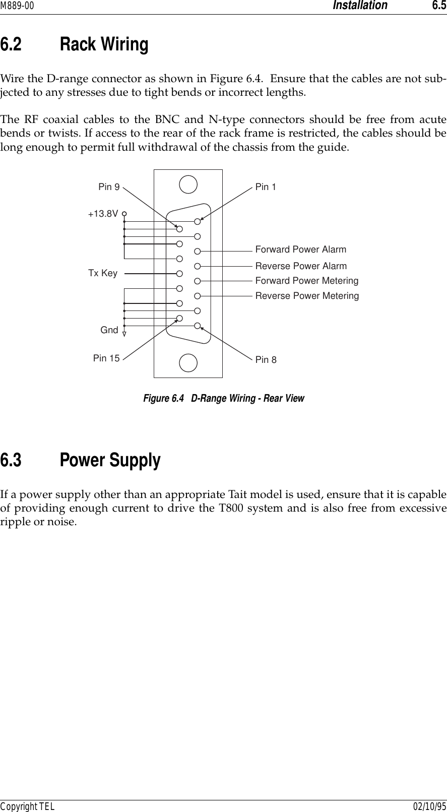
CalAmp Wireless Networks BDD4T889 User Manual d ipn docs m889 00 100 88900 0 100

CALAMP WIRELESS NETWORKS INC. d ipn docs m889 00 100 88900 0 100

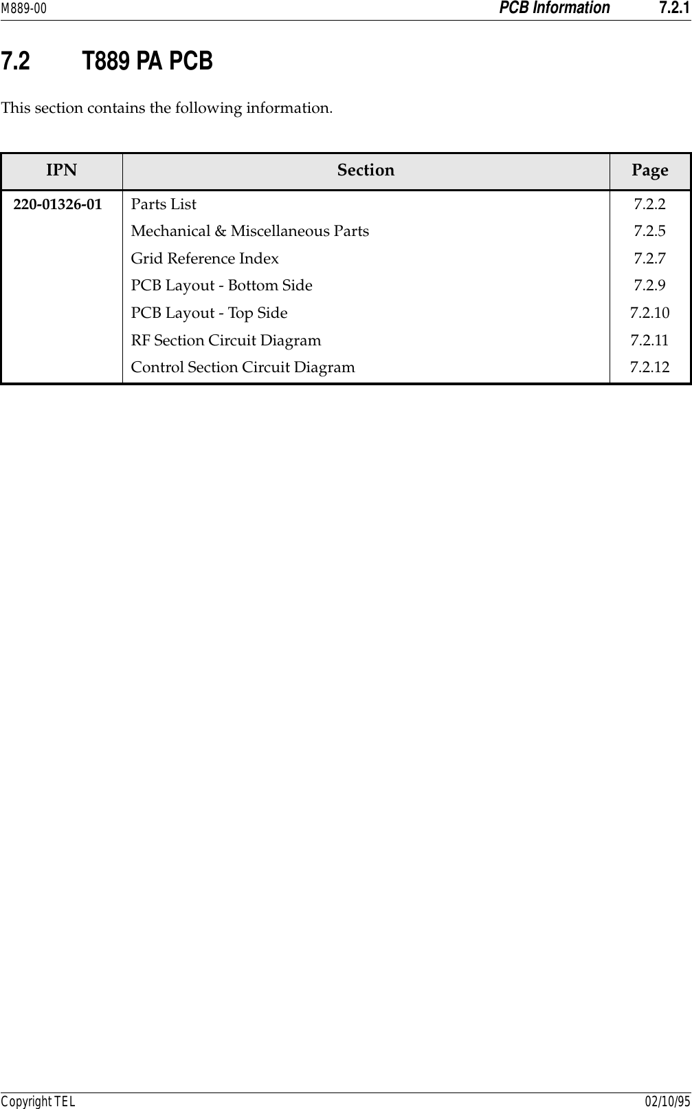
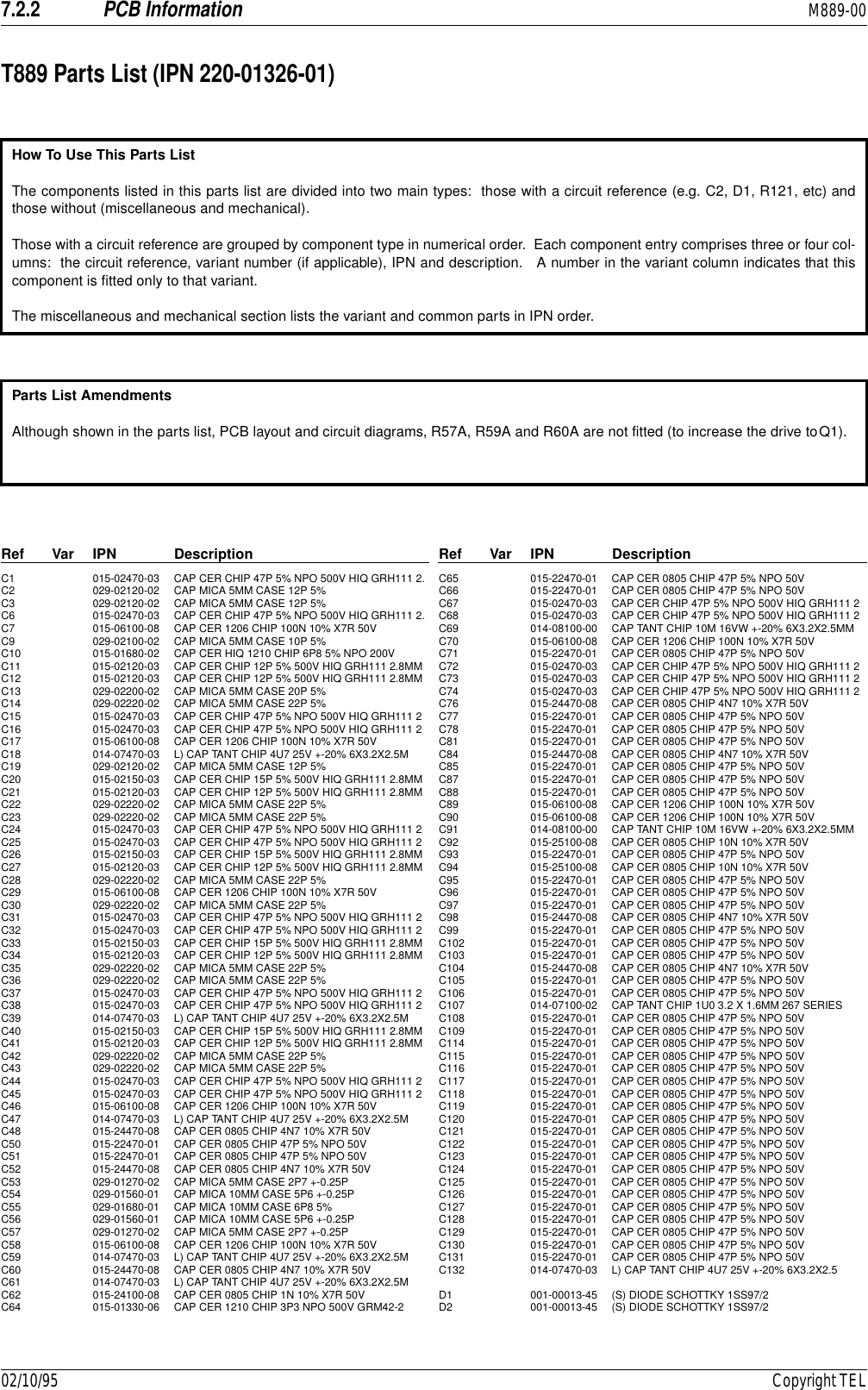
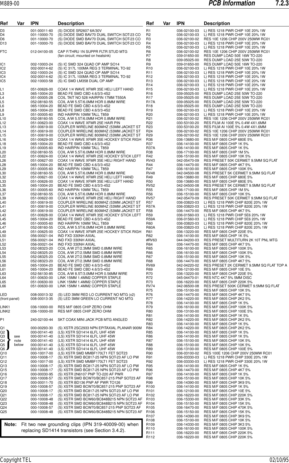
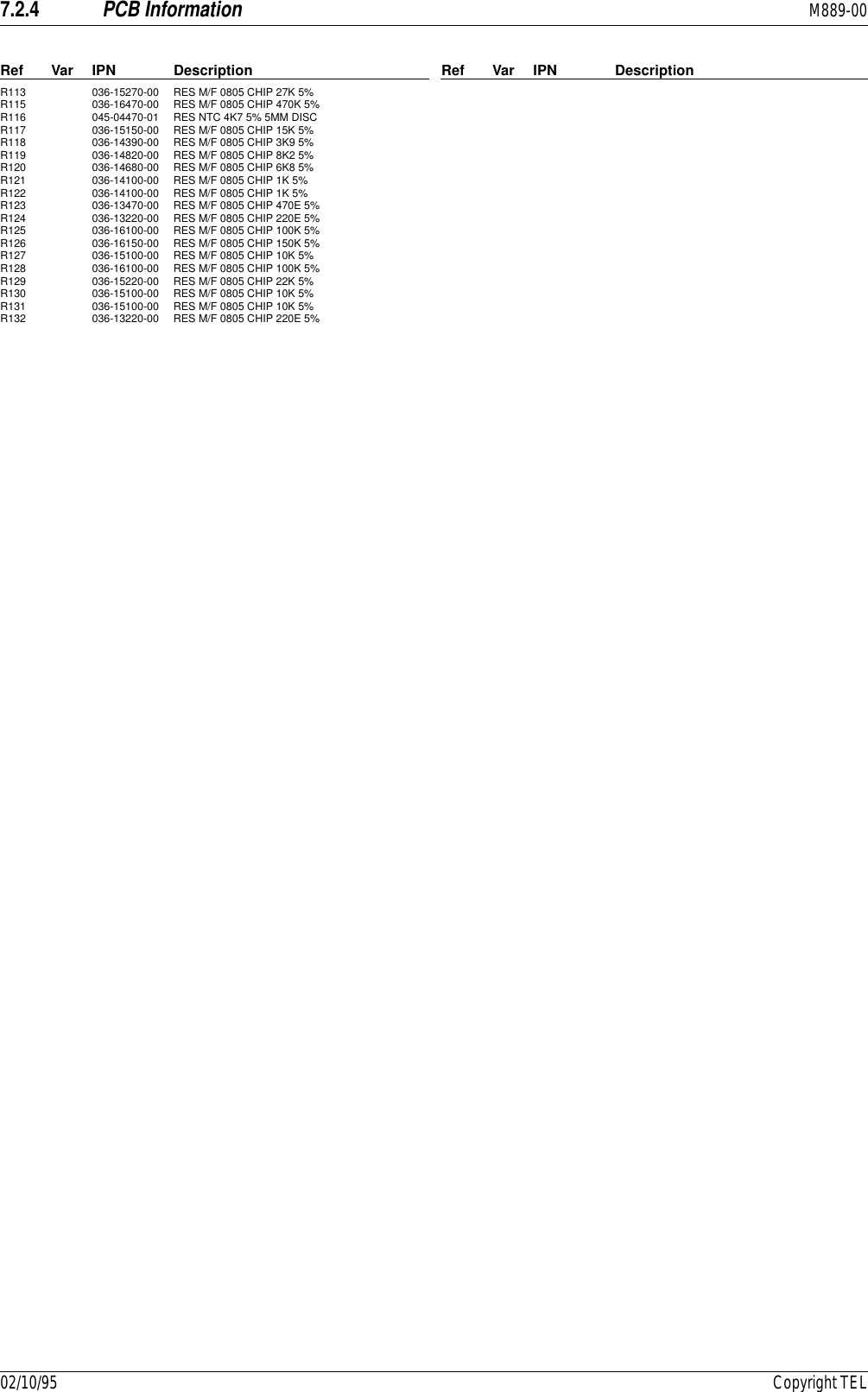
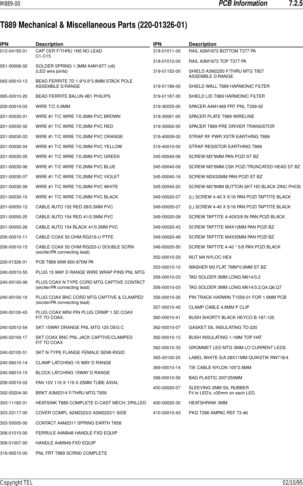
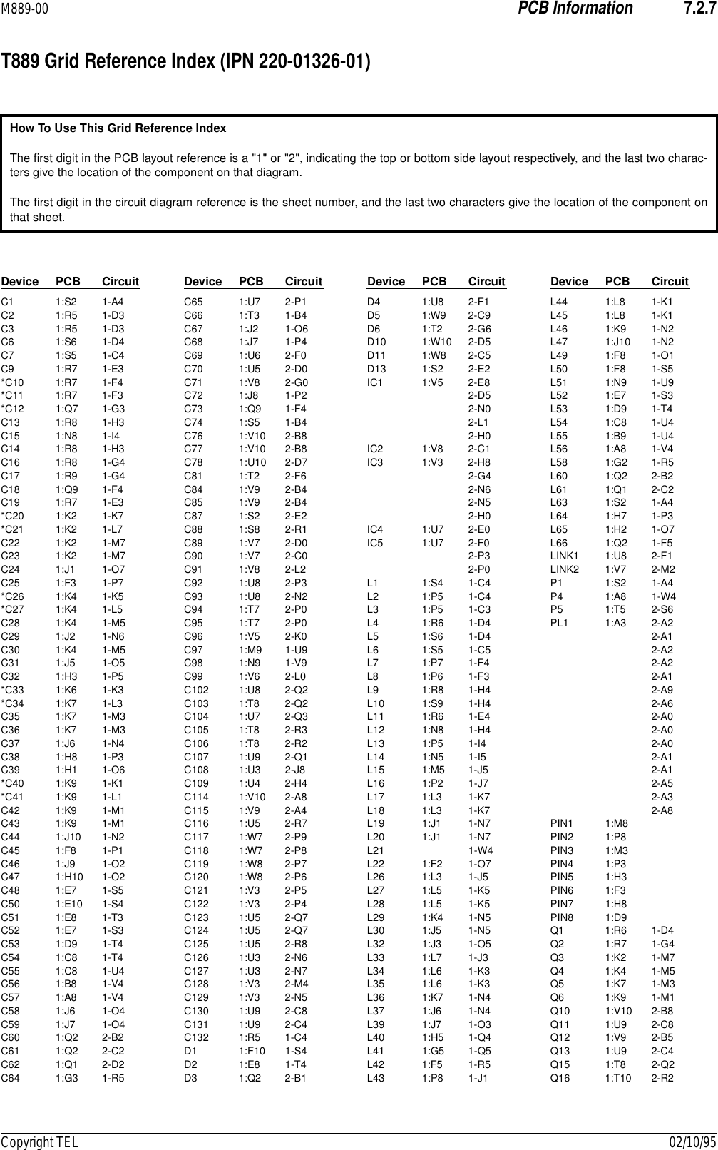
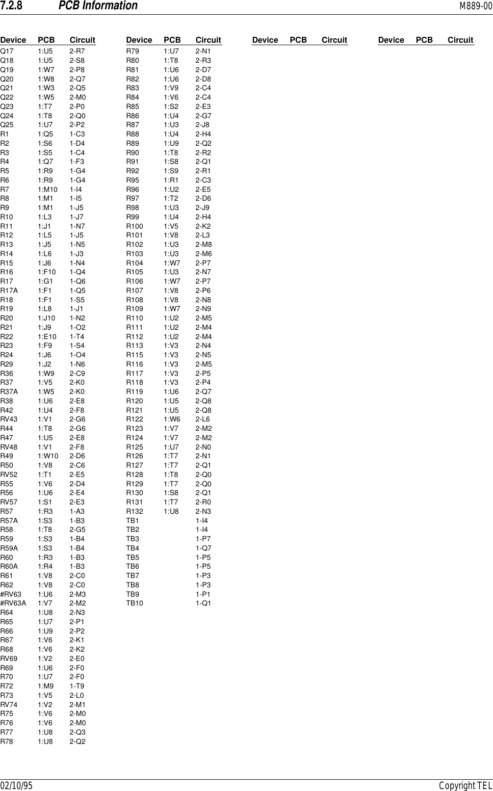
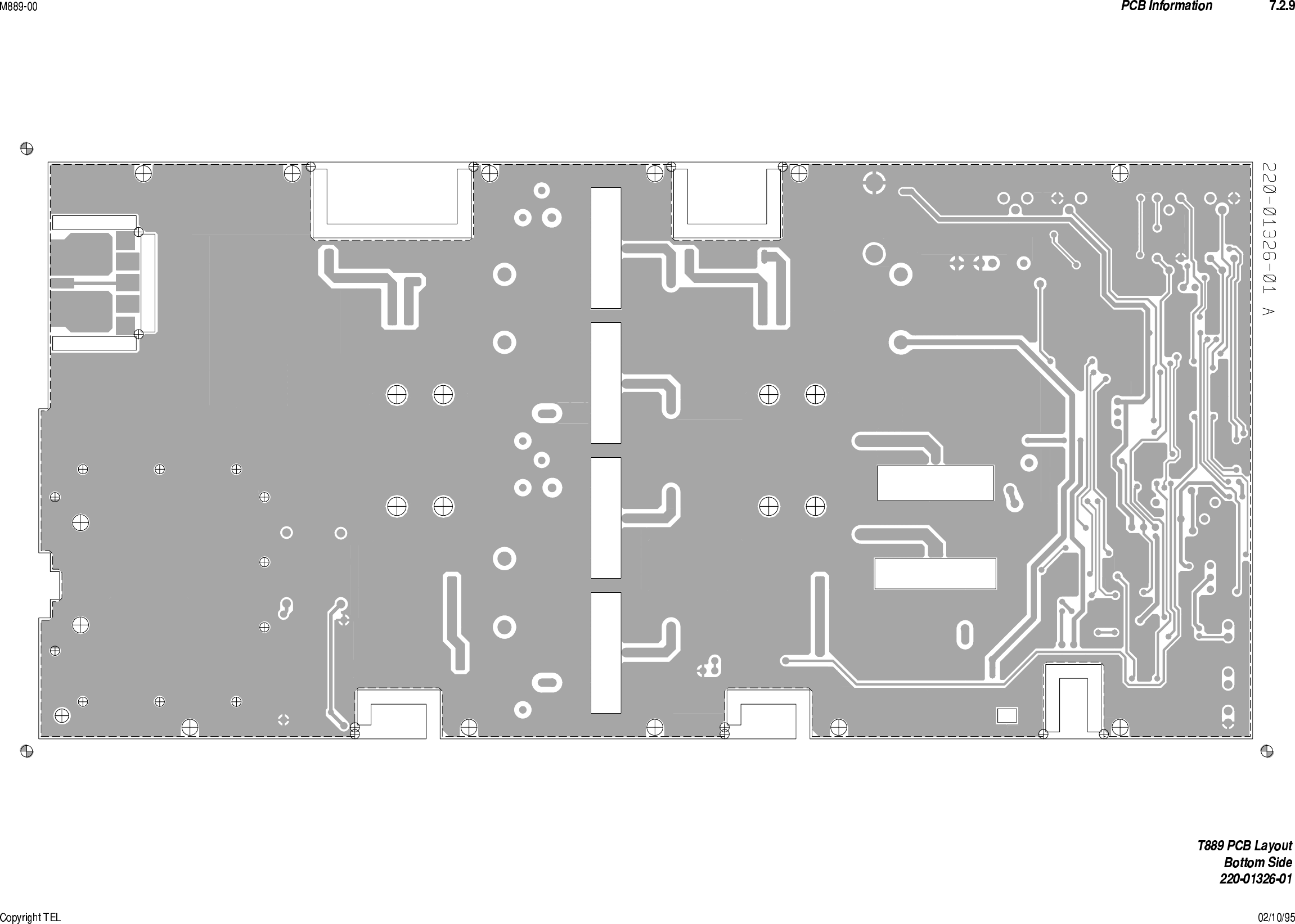
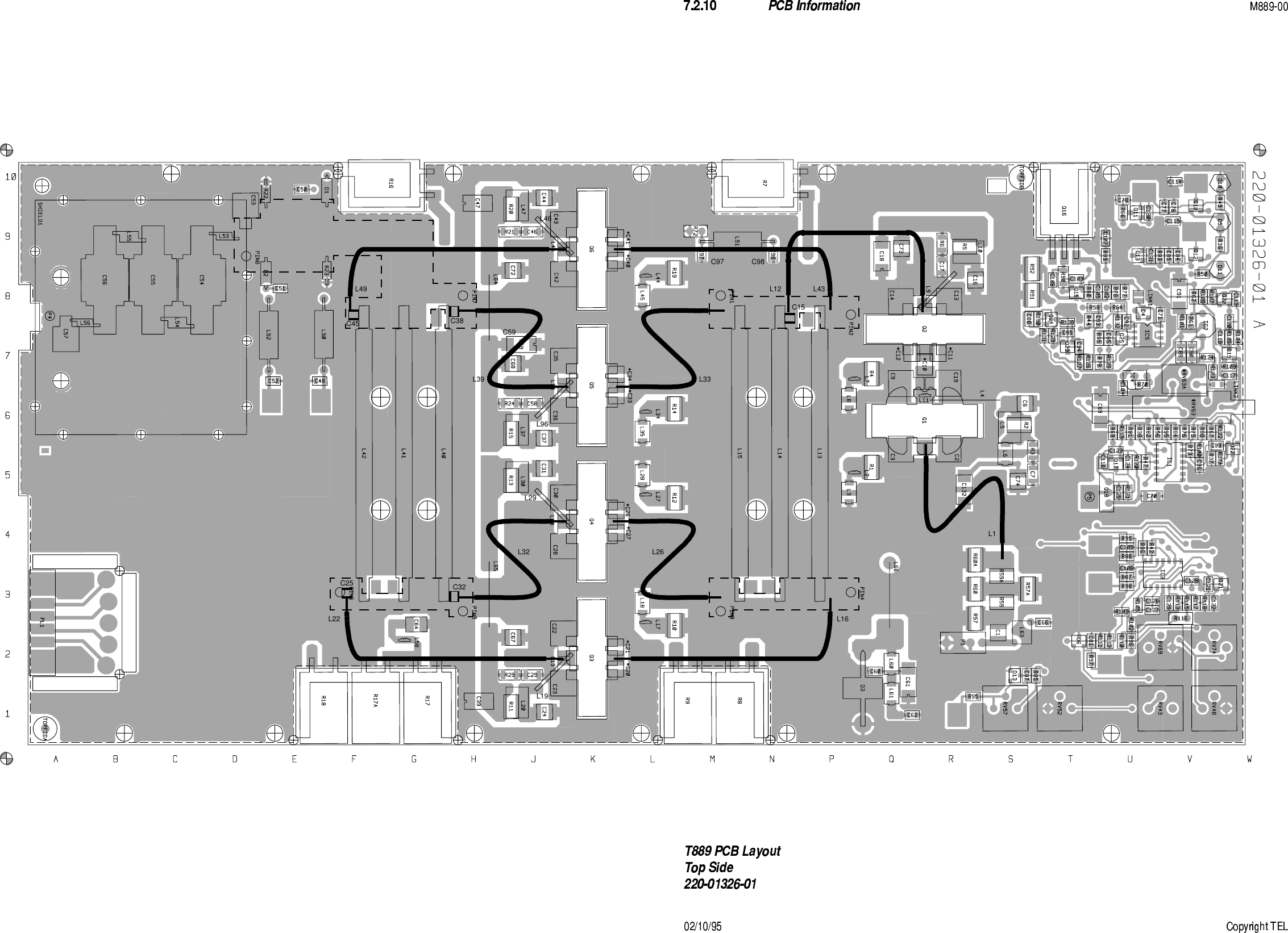
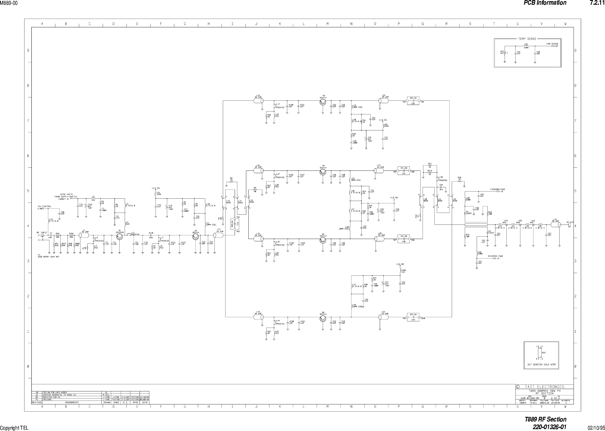
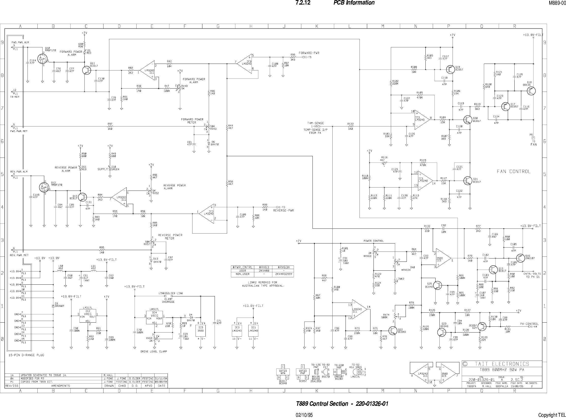
user manual provided for PA module T889

M889-00 1Copyright TEL 02/10/95T889 Power AmplifierUHF FM 800-870MHzIssue 100 October 1995M889-00-100
2M889-0002/10/95 Copyright TELHead OfficeNew ZealandTait Electronics Ltd558 Wairakei RoadP.O. Box 1645ChristchurchNew ZealandPhone:  64 3 358-3399Fax:  64 3 358-3636AustraliaTait Electronics (Aust) Pty Ltd275 Toombul RoadNorthgate 4013P.O. Box 679VirginiaQueensland 4014AustraliaPhone: 61 7 3260-7799Toll Free: 1800 077-112Fax: 61 7 3260-7990CanadaTait Mobile Radio Inc.Unit 5, 158 Anderson AvenueMarkhamOntario L6E1A9CanadaPhone:  1 905 472-1100Toll Free:  1 800 890-8248Fax:  1 905 472-5300FranceTait France Sarl2 Avenue de la Cristallerie92 316 Sèvres, CedexFrancePhone:  33 1 41 14-05-50Fax:  33 1 41 14-05-55GermanyTait Mobilfunk GmbHWillstätterstraße 50D-90449 Nürnberg 60GermanyPhone:  49 911 96 746-0Fax: 49 911 96 746-79New ZealandTait Communications LtdUnit 4, 75 Blenheim RoadP.O. Box 1185ChristchurchPhone:  64 3 348-3301Fax:  64 3 343-0558SingaporeTait Electronics (Far East) Pte Ltd4 Leng Kee RoadSIS Building #05-11ASingapore 159088Phone:  65 471-2688Fax:  65 479-7778United KingdomTait Mobile Radio LtdErmine Business ParkErmine RoadHuntingdonCambridgeshire PE18 6YAUnited KingdomPhone: 44 1480-52255Fax: 44 1480-411996USATait Electronics (USA) Inc.9434 Old Katy RoadSuite 110HoustonTexas 77055USAPhone: 1 713 984-8684Toll Free: 1 800 222-1255Fax: 1 713 468-6944
M889-00 3Copyright TEL 02/10/95About This ManualScope This manual contains general, technical and servicing informa-tion on the T889 Power Amplifier.Revision Control Each page in this manual has a date of issue.  This is to complywith various Quality Standards, but will also serve to identifywhich pages have been updated and when.  Each page and itspublication date is listed in the “List of Effective Pages”.Any portion of text that has been changed is marked by a verti-cal line (as shown at left) in the outer margin of the page.  Wherethe removal of an entire paragraph means there is no text left tomark, an arrow (as shown at left) will appear in the outer mar-gin.  The number beside the arrow will indicate how many para-graphs have been deleted.The manual issue and revision status are indicated by the lastthree digits of the manual IPN. These digits start at 100 and willincrement through 200, 300, etc., as the manual is updated andrepublished, e.g:  The last two digits are used for manuals published in an updata-ble ring binder format and do not apply to this manual.PCB Information PCB information is provided for all current issue PCBs, as wellas all previous issue PCBs manufactured in production quanti-ties, and is grouped according to PCB.  Thus, you will find theparts list, grid reference index (if necessary), PCB layouts andcircuit diagram(s) for each individual PCB grouped together.Errors If you find an error in this manual, or have a suggestion on howit might be improved, please do not hesitate to contact the Tech-nical Writer, Radio Infrastructure Division, Tait Electronics Ltd,P.O. Box 1645, Christchurch, New Zealand.Technical InformationAny enquiries regarding this manual or the equipment it describes should be addressedin the first instance to your nearest approved Tait Dealer or Service Centre.  Furthertechnical assistance may be obtained from the Customer Support Group, Radio Infra-structure Division, Tait Electronics Ltd, Christchurch, New Zealand.Updating Equipment And ManualsIn the interests of improving performance, reliability or servicing, Tait Electronics Ltdreserve the right to update their equipment and/or manuals without prior notice.21  0  0issue status revision status
4M889-0002/10/95 Copyright TELCopyrightAll information contained in this manual is the property of Tait Electronics Ltd. Allrights are reserved.  This manual may not, in whole or part, be copied, photocopied,reproduced, translated stored or reduced to any electronic medium or machine readableform without prior written permission from Tait Electronics Ltd.Ordering Tait Service ManualsService Manuals should be ordered from your nearest Tait Branch or approved Dealer.When ordering, quote the Tait Internal Part Number (IPN) and, where applicable, theversion.Date Of IssueIPN M889-00-100 T889 Power Amplifier Service Manual Issue 100 published October 1995
M889-00 5Copyright TEL 02/10/95Table Of ContentsThis manual is divided into seven Sections as listed below.  There is a detailed table ofcontents at the start of each Section.Section Title1 General Information2 Circuit Operation3 Introduction To Servicing4 Initial Tuning & Adjustment5 Fault Finding6 Installation7 PCB Information
6M889-0002/10/95 Copyright TELList Of Effective PagesThe total number of pages in this Manual is 64, as listed below. Page Issue Date Page Issue Date102/10/95202/10/95302/10/95402/10/95502/10/95602/10/951.1 02/10/951.2 blank1.3 02/10/951.4 02/10/951.5 02/10/951.6 02/10/952.1 02/10/952.2 blank2.3 02/10/952.4 02/10/952.5 02/10/952.6 02/10/953.1 02/10/953.2 blank3.3 02/10/953.4 02/10/953.5 02/10/953.6 02/10/953.7 02/10/953.8 02/10/953.9 02/10/953.10 02/10/954.1 02/10/954.2 blank4.3 02/10/954.4 02/10/955.1 02/10/955.2 blank5.3 02/10/955.4 02/10/955.5 blank (fold-out)5.6 02/10/95 (fold-out)5.7 02/10/955.8 02/10/955.9 02/10/955.10 blank6.1 02/10/956.2 blank6.3 02/10/956.4 02/10/956.5 02/10/956.6 blank7.1.1 02/10/957.1.2 blank7.1.3 02/10/957.1.4 02/10/957.2.1 02/10/957.2.2 02/10/957.2.3 02/10/957.2.4 02/10/957.2.5 02/10/957.2.6 blank7.2.7 02/10/957.2.8 02/10/957.2.9 02/10/95 (fold-out)7.2.10 02/10/95 (fold-out)7.2.11 02/10/95 (fold-out)7.2.12 02/10/95 (fold-out)
M889-00 General Information 1.1Copyright TEL 02/10/951 General InformationThis section provides a brief description of the T889 PA, along with detailed specifica-tions and a list of variants available.The following topics are covered in this section.Section Title Page1.1 Introduction 1.31.21.2.11.2.2SpecificationsIntroductionGeneral1.41.41.41.3 Versions 1.6
1.2 General Information M889-0002/10/95 Copyright TEL
M889-00 General Information 1.3Copyright TEL 02/10/951.1 IntroductionThe T889 is an FM base station power amplifier designed for single or multichanneloperation within the frequency range 800 to 870MHz.  The output power capability is 20to 100W.The PA comprises a broad band, two stage drive amplifier whose output is split to drivefour separate output stages.  The outputs from these final stages are then recombinedand filtered before being fed to the output socket.  This type of balanced output stageoffers two advantages over single ended types:- improved intermodulation performance in the presence of high signal levelsfrom adjacent transmitters;- enhanced reliability:  if one of the four output stages fails, the transmitter canstill produce half its rated power.VSWR and thermal protection is incorporated into the basic design, while monitoringand alarm signals are available for both forward and reverse power.  The output poweris adjustable from the front panel.The main PCB is mounted directly on a die-cast chassis/heatsink.  For long-term relia-bility, four high quality, low loss Teflon PCBs are sweated to the main PCB in areas ofhigh RF current.  Extensive use is also made of the latest surface mount technology.Forced air cooling for the heatsink is provided on the T889 by a fan, which is activatedwhenever the transmitter is keyed.  Thermal sensors will also activate the fan automati-cally if the internal temperature reaches an unacceptable level.The T889 has a width of 120mm, occupying a double module in a Tait rack shelf(T99-770) which will accommodate up to seven standard modules to give an attractiveand convenient installation.
1.4 General Information M889-0002/10/95 Copyright TEL1.2 Specifications1.2.1 IntroductionThe performance figures given are minimum figures, unless otherwise indicated, forequipment tuned with the maximum switching band and operating at standard roomtemperature (+22°C to +28°C).Where applicable, the test methods used to obtain the following performance figures arethose described in the EIA specification.  However, there are several parameters forwhich performance according to the CEPT specification is given.Details of test methods and the conditions which apply for Type Approval testing in allcountries can be obtained from Tait Electronics Ltd.1.2.2 GeneralPower Output: Rated Power  .. 90W Range Of Adjustment  .. 20 to 100W (typical) Duty Cycle Rating:  .. 90W continuous to +60°CIntermodulation  .. -70dBc or -40dBi1 with 25dB isolation(PA with output isolator)  & interfering signal of -30dBcMismatch Capability: Ruggedness .. infinite VSWR Stability  .. 5:1 VSWR (all phase angles)Supply Voltage: Operating Voltage  .. 10.8 to 16V DC Standard Test Voltage  .. 13.8V DC Polarity .. negative earth only Polarity Protection  .. diodeSupply Current:Standby .. 50mA Transmit .. 27A (20A typical @ 850MHz)1. dBi denotes the level of the intermodulation product relative to the interfering signal.
M889-00 General Information 1.5Copyright TEL 02/10/95Spurious Emissions: Conducted - Transmit  .. -36dBm to 1GHz -30dBm to 4GHz - Standby  .. -57dBm to 1GHz -47dBm to 4GHzRadiated - Transmit  .. -36dBm to 1GHz -30dBm to 4GHz - Standby   .. -57dBm to 1GHz -47dBm to 4GHzDimensions: Height .. 191mm Width .. 120mm Length .. 340mmWeight: .. 3.5kg
1.6 General Information M889-0002/10/95 Copyright TEL1.3 VersionsDescription Version10800-870MHz
M889-00 Circuit Operation 2.1Copyright TEL 02/10/952 Circuit OperationThis section provides a basic description of the circuit operation of the T889 PA.The following topics are covered in this section.Section Title Page2.1 Introduction 2.32.2 RF Circuitry 2.32.32.3.12.3.22.3.32.3.42.3.52.3.6Control CircuitryPower ControlDriver Power LevelThermal ProtectionForward And Reverse Power AlarmsForward And Reverse Power MeteringFan Control Circuitry2.42.52.52.52.52.62.6Figure Title Page2.12.22.3High Level Block DiagramControl Circuitry Block DiagramFan Control Logic Diagram2.32.42.6
2.2 Circuit Operation M889-0002/10/95 Copyright TEL
M889-00 Circuit Operation 2.3Copyright TEL 02/10/952.1 IntroductionFigure 2.1   High Level Block DiagramThe T889 comprises a three stage RF power amplifier with extensive control circuitry.The final stage is composed of four transistors (Q3, Q4, Q5 & Q6) whose outputs arecombined to provide the rated output power.The configuration of each of the main circuit blocks may be seen on a functional level inFigure 2.1.2.2 RF CircuitryThe driver stage of the T889 consists of a two stage transistor amplifier (Q1, Q2) whichdelivers a minimum of 40W.  This signal is split via three 3dB couplers (L13, L14 & L15)and used to drive the four final amplifiers (Q3, Q4, Q5 & Q6).  These outputs are recom-bined by L40, L41 & L42 and passed to the antenna socket via the directional couplerand low pass filter.The directional coupler senses forward and reflected power, which is rectified (D1, D2)and passed to the control circuitry for metering, alarm and power control purposes.Power control is via a series pass transistor (Q16), which controls the supply voltage onthe collector of the driver transistor (Q1).RF OutQ1 Q2PadRF In LPF4W 40WQ3Q4Q5Q630W30W30W30W60W60W120W 100WPowerControl VsupplyQ16L40L13L15 L42L14 L41DirectionalCoupler
2.4 Circuit Operation M889-0002/10/95 Copyright TEL2.3 Control CircuitryFigure 2.2   Control Circuitry Block DiagramREF
M889-00 Circuit Operation 2.5Copyright TEL 02/10/952.3.1 Power ControlThe DC voltages from the directional coupler representing forward and reflected powerare buffered by the two voltage followers, IC3 pins 1, 2 & 3 and pins 5, 6 & 7.  Their out-puts are summed at an integrator (IC1 pins 8, 9 & 10), which drives the series pass con-trol element (Q16).Forward and reflected power are summed so that, under high output VSWR, the powercontrol turns the PA down.  This is because the control loop adjusts for the same DCvoltage from the directional coupler that would have been present if there were noreflected power.2.3.2 Driver Power LevelThe maximum output power of the T889 can be limited by placing a ceiling on thedriver output power level using RV69 (accessible through the side cover).  For example,if RV69 is set for a maximum output power of 50W, the range of adjustment using RV63(front panel power adjust) will be 20 to 50W.2.3.3 Thermal ProtectionAt excessively high temperatures, the output power will automatically reduce to a pre-set level (set by RV74), thus preventing the PA from overheating.A thermistor controlled voltage divider (R68, R72) applies a voltage to a comparatorwith hysteresis (IC1 pins 12, 13 & 14).  The output current from the comparator is summed into the power control network viaRV74 so that the power level to which the PA must turn down may be set.2.3.4 Forward And Reverse Power AlarmsIf forward power drops below, or reverse power rises above, presettable limits, alarmsmay be triggered.The alarm outputs are open drain configuration and are low under normal conditions(i.e. forward and reverse power levels are normal).IC1 pins 1, 2 & 3 and pins 5, 6 & 7 form comparators with thresholds adjusted via RV48and RV52 respectively.  The inputs are from the forward and reverse power signals fromthe directional coupler, buffered by IC3 pins 1, 2 & 3 and pins 5, 6 & 7.  Thus, the powerlevels at which the forward and reverse power alarms are triggered are defined by RV48and RV52 respectively.
2.6 Circuit Operation M889-0002/10/95 Copyright TEL2.3.5 Forward And Reverse Power MeteringForward and reverse power signals from the two IC3 buffers are available for meteringpurposes.  The output currents are adjustable via RV43 (forward power) and RV57(reverse power).2.3.6 Fan Control CircuitryFigure 2.3   Fan Control Logic DiagramComparator IC3 pins 8, 9 & 10 are set to trigger at heatsink temperatures greater than+70°C, and pins 12, 13 & 14 at temperatures greater than -10°C.A logic AND function is applied to the comparator outputs by Q20 and Q21, therebyturning on the fan unconditionally (via Q17 and Q18) if the heatsink temperatureexceeds +70°C.A logic OR function is applied to comparator IC3 pins 8, 9 & 10 and Tx KEY signals,thereby turning on the fan when the transmitter is keyed and the temperature isbetween -10°C and +70°C.If the temperature drops below -10°C, Q21 is turned off, preventing either Q19 or Q20from activating the fan.Q17 Q18 FanRef+High Temp.SenseComparatorIC3CR72Ref+Low Temp.SenseComparatorIC3DR116NTCNTCTx KeyInvertQ19 ORQ20,R106, R107NANDQ20, Q21,R119, R120 Fan Driver13.8VFiltered
M889-00 Introduction To Servicing 3.1Copyright TEL 02/10/953 Introduction To ServicingThis section provides some general and advisory information on servicing procedures.The following topics are covered in this section.Section Title Page3.13.1.13.1.23.1.3GeneralCaution:  CMOS DevicesCaution:  Aerial LoadCaution:  Beryllium Oxide & Power Transistors3.33.33.33.43.23.2.13.2.23.2.33.2.4MechanicalPozidriv Recess Head ScrewsUNC Thread ScrewsScrew TorquesDisassembly/Reassembly3.53.53.53.53.53.33.3.13.3.1.13.3.1.23.3.2Component ReplacementLeaded ComponentsDesoldering Iron MethodComponent Cutting MethodSurface Mount Devices3.63.63.63.63.73.43.4.13.4.1.13.4.1.23.4.2To Replace PA TransistorsCapacitor /Transistor SpacingQ1 (2SC2933 Pre-Driver)Q2, Q3, Q4, Q5 & Q6 (SD1414)Replacement Procedure3.83.83.83.83.83.5 To Remove The PCB From The Heatsink 3.103.6 To Remove Cased Mica Capacitors 3.10Figure Title Page3.1 Typical Anti-static Bench Set-up 3.33.2 Typical Transistor/Capacitor Spacing (Q1 & Q2 Shown) 3.9
3.2 Introduction To Servicing M889-0002/10/95 Copyright TEL
M889-00 Introduction To Servicing 3.3Copyright TEL 02/10/953.1 GeneralIf you require further information about the T889 or this manual, contact your nearestauthorised Tait Dealer or Service Centre.  Further assistance may be obtained from theCustomer Support Group, Radio Infrastructure Division, Tait Electronics Ltd, Christch-urch, New Zealand.When requesting this information, please quote the equipment type number (e.g.T889-10) and serial number.  In the case of the service manual quote the Tait InternalPart Number (IPN), e.g. M889-00-100, and for circuit diagrams quote the “Title”, “IPN”and “Issue”.3.1.1 Caution:  CMOS DevicesThis equipment contains CMOS Devices which are susceptible to damage from staticcharges.  Care when handling these devices is essential.  For correct handling proce-dures refer to the manufacturers' data books, e.g. Philips data books covering CMOSdevices, or Motorola CMOS data books, Section 5 “Handling”, etc.Figure 3.1   Typical Anti-static Bench Set-upAn anti-static bench kit (refer to Figure 3.1) is available from Tait Electronics Ltd underthe usual consumable goods ordering system.  The kit is held in stock under IPN937-00000-34 and contains:1 conductive rubber bench mat 1 earth lead to connect the mat to ground (c/w 1M series resistor) 1 wrist strap information leaflet.3.1.2 Caution:  Aerial LoadThe equipment has been designed to operate safely under a wide range of aerial loadingconditions.  However, it is strongly recommended that the transmitter should not beoperated in the absence of a suitable load.  Failure to observe this warning may result indamage to the transmitter output power stage.conductive rubberbench matmetal frameto building earth (not mains earth) via 1M series resistorconductivewrist strap
3.4 Introduction To Servicing M889-0002/10/95 Copyright TEL3.1.3 Caution:  Beryllium Oxide & Power TransistorsThe RF power transistors in current use all contain some beryllium oxide.  This sub-stance, while perfectly harmless in its normal solid form, can become a severe healthhazard when it has been reduced to dust.  For this reason the RF power transistorsshould not be broken open, mutilated, filed, machined, or physically damaged in anyway that can produce dust particles.
M889-00 Introduction To Servicing 3.5Copyright TEL 02/10/953.2 Mechanical3.2.1 Pozidriv Recess Head ScrewsPozidriv recess head screws are the preferred standard on all Tait manufactured equip-ment.  The very real advantages of this type of screw will not be realised unless the cor-rect screwdrivers are used by servicing personnel.3.2.2 UNC Thread ScrewsAll black finish Pozidriv screws used in the T889 are 4-40 UNC thread and cannot beinterchanged with M3 screws.  Note that different lengths are used in different applica-tions.3.2.3 Screw TorquesIt is important to tighten the cover and power transistor securing screws to the correcttorque to ensure that the T889 maintains its specified performance. We recommend the following torque settings:cover screws .. 6lb-in./0.7Nmpower transistors .. 6lb-in./0.7Nm3.2.4 Disassembly/ReassemblyThe power output level setting procedures should be carried out with the cover on.
3.6 Introduction To Servicing M889-0002/10/95 Copyright TEL3.3 Component Replacement3.3.1 Leaded ComponentsWhenever components are removed from or fitted to the PCB, care must be taken toavoid damage to the track.  The two satisfactory methods of removing components fromPTH PCBs are detailed below.Note: The first method requires the use of a desoldering station, e.g. Philips SBC314 or Pace MBT-100E.3.3.1.1 Desoldering Iron MethodPlace the tip over the lead and, as the solder starts to melt, move the tip in a circu-lar motion.Start the suction and continue the movement until 3 or 4 circles have been com-pleted.Remove the tip while continuing suction to ensure that all solder is removed fromthe joint, then stop the suction.Before pulling the lead out, ensure it is not stuck to the plating.If the lead is still not free, resolder the joint and try again.Note: The desoldering iron does not usually have enough heat to desolder leadsfrom the ground plane.  Additional heat may be applied by holding a sol-dering iron on the tip of the desoldering iron (this may require some addi-tional help).3.3.1.2 Component Cutting MethodCut the leads on the component side of the PCB.Heat the solder joint sufficiently to allow easy removal of the lead by drawing itout from the component side:  do not use undue force.Fill the hole with solder and then clear with solderwick.
M889-00 Introduction To Servicing 3.7Copyright TEL 02/10/953.3.2 Surface Mount DevicesCaution: Surface mount devices (SMD's) require special storage, handling,removal and replacement techniques.  This equipment should be serv-iced only by an approved Tait Dealer or Service Centre equipped withthe necessary facilities.  Repairs attempted with incorrect equipment orby untrained personnel may result in permanent damage.  If in doubt,contact Tait Electronics Ltd or your nearest Tait Branch or Subsidiary.
3.8 Introduction To Servicing M889-0002/10/95 Copyright TEL3.4 To Replace PA TransistorsCaution: As the location of certain components in the PA is critical to perform-ance, it is important that any components removed or disturbed arerefitted in EXACTLY the same position.Caution: Do not solder the tabs before torquing down otherwise the device maybe broken.3.4.1 Capacitor /Transistor SpacingRefer to Figure 3.2.3.4.1.1 Q1 (2SC2933 Pre-Driver)Before attempting to remove Q1, measure the distance between the capacitorslabelled “c” and the transistor body (measurement “a”) so that the capacitors canbe replaced in exactly the same position.  Note: Be sure to measure between the transistor body and the tabs (not the body)of the capacitors.Position the capacitors labelled “b” hard up against the transistor body.3.4.1.2 Q2, Q3, Q4, Q5 & Q6 (SD1414)Position all capacitors labelled “b” hard up against the transistor body.3.4.2 Replacement ProcedureDesolder the tabs (and grounding clips if an SD1414) by heating with a solderingiron and lifting away from the PCB with a thin stainless steel spike, or screw-driver.Unscrew the transistor and remove the device.Smear the face of the replacement device with heatsink compound and tighten itsecurely (torque setting 6lb-in./0.7Nm) to the heatsink.  If you are replacing anSD1414, remember to fit new grounding clips.Solder the tabs.Replace each capacitor as instructed in Section 3.4.1.
M889-00 Introduction To Servicing 3.9Copyright TEL 02/10/95Figure 3.2   Typical Transistor/Capacitor Spacing (Q1 & Q2 Shown)Grounding Clipsbbbbbccbmeasurement aQ1Q2
3.10 Introduction To Servicing M889-0002/10/95 Copyright TEL3.5 To Remove The PCB From The HeatsinkMost components are soldered topside only, but in some cases access to the underside ofthe PCB is necessary.Remove the D-range connector.Disconnect the power feed to the fan.Remove the 13 PCB retaining screws (2 are hidden beneath the harmonic filtershield).Remove the transistor mounting screws.Remove the mounting screws for the TO-220 devices:R6, R7, R9, R16, R17, R17a and R18.Remove the retaining screws for the wireline couplers (L13, L14, L15, L40, L41 andL42).Remove the output 50 ohm coaxial connector by unscrewing it from the heatsinkcasting and desoldering it from the PCB.Disconnect the input 50 ohm coaxial cable by unplugging it at the PCB.Disconnect the battery positive and negative feed wires from the PCB.Disconnect the alarm and metering wires from the PCB.Lift the PCB gently from the heatsink to gain access to the underside of the PCB.Caution: Do not operate the PA with the PCB detached as the heatsink is usedfor earthing and for the dissipation of heat generated within the tran-sistors.To replace the PCB, reverse the order of removal, taking care that the wiring is cor-rectly routed and is not subjected to 'pinching'.3.6 To Remove Cased Mica CapacitorsCased mica capacitors can be removed by heating the top with a heavy-duty solderingiron and gently lifting the capacitor off the PCB with a solder-resistant spike or equiva-lent.
M889-00 Initial Tuning & Adjustment 4.1Copyright TEL 02/10/954 Initial Tuning & AdjustmentThe following section describes the initial set-up procedures, including alarm adjust-ment and power meter calibration.The following topics are covered in this section.Section Title Page4.1 Initial Connections 4.34.2 RF Alignment 4.34.3 High Temperature Shutdown Power Level 4.34.4 Low Forward Power Alarm 4.34.5 High Reverse Power Alarm 4.44.6 Remote Forward Power Meter Calibration 4.44.7 Remote Reverse Power Meter Calibration 4.4
4.2 Initial Tuning & Adjustment M889-0002/10/95 Copyright TEL
M889-00 Initial Tuning & Adjustment 4.3Copyright TEL 02/10/954.1 Initial ConnectionsConnect the PA to a power supply, an output RF load and a power meter asdetailed below:power supply rating >30ARF load >150W.Provide a keyed RF drive at the required frequency.Connect the drive source key line to pin 12 of the external connector.Set RV69 (temperature shutdown) fully anticlockwise to avoid RF power cyclingbetween the levels as set by RV63 and RV74.4.2 RF AlignmentSet RV63 (power control) fully clockwise.Key on the drive source (the power output should exceed 100W).Adjust RV69 (driver power level) until the output power drops to 100W.Adjust RV63 to reduce the power output to the required level (e.g. 90W).4.3 High Temperature Shutdown Power LevelSet RV63 (power control) to the required output power.Earth pin 12 of IC1 (the pad at NTC R72 is convenient).Adjust RV74 (shutdown power level) for an output power of 20W.Remove the earth from pin 12 of IC1.4.4 Low Forward Power AlarmSet RV63 (power control) to the output power at which the alarm is required toactivate.Adjust RV48 (forward power alarm) until the front panel LED just lights.Reset RV63 to the required output power.Note: Remote indication is available at D-range pin 3.
4.4 Initial Tuning & Adjustment M889-0002/10/95 Copyright TEL4.5 High Reverse Power AlarmSet RV63 to the required output power.Connect a known mismatch of the required value to the PA output.Apply RF drive and Tx key.Adjust RV52 (reverse power alarm) so that the front panel high reverse powerLED just lights.Example: A VSWR of 3:1 can be simulated by connecting an unterminated 150W3dB pad to the PA output.  This will result in a return loss of 6dB.Note: Remote indication is available at D-range pin 4.4.6 Remote Forward Power Meter CalibrationIf a remote meter is connected, adjust RV43 (forward power meter) for the remotereading to agree with the RF power meter reading.4.7 Remote Reverse Power Meter CalibrationIf a remote meter is connected, connect a 50 ohm 3dB pad (with the output opencircuit) to the PA output.Apply RF drive and Tx key.Adjust RV57 (reverse power meter) for a quarter of the forward power reading.
M889-00 Fault Finding 5.1Copyright TEL 02/10/955 Fault FindingThe following test procedures and fault finding flow charts may be used to help locate ahardware problem, however they are by no means a complete fault finding procedure.If the fault still exists after having progressed through them in a logical manner, contactyour nearest authorised Tait Dealer or Service Centre.  Further assistance may beobtained from the Customer Support Group, Radio Infrastructure Division, Tait Elec-tronics Ltd, Christchurch, New Zealand.The following topics are covered in this section.Section Title Page5.1 Visual Checks 5.35.2 Component Checks 5.35.3 DC Checks 5.35.4 RF Checks 5.45.55.5.15.5.25.5.3Fault Finding ChartsPAPower ControlFan Control Circuitry5.75.75.85.9Figure Title Page5.1 Positioning Of Test Leads For Q1-Q6 5.6
5.2 Fault Finding M889-0002/10/95 Copyright TEL
M889-00 Fault Finding 5.3Copyright TEL 02/10/955.1 Visual ChecksRemove the cover from the T889 and inspect the PCB for damaged or broken com-ponents, paying particular attention to the surface mounted devices (SMD's).Check for defective solder joints.  If repair or replacement is considered necessary,refer to Sections 3.3, 3.4, 3.5 and 3.6.5.2 Component ChecksIf a transistor is suspected of faulty operation, an indication of its performance can beassessed by measuring the forward and reverse resistance of the junctions. First makesure that the transistor is not shunted by some circuit resistance (unless the device iscompletely desoldered).  A 20k ohm/V or better multimeter should be used for takingthe measurements, using only the medium or low resistance ranges.The collector current drawn by multi-junction transistors is a further guide to their per-formance.If an IC is suspect, the most reliable check is to measure the DC operating voltages. Dueto the catastrophic nature of most IC failures, the pin voltages will usually be markedlydifferent from the recommended values in the presence of a fault.  The recommendedvalues can be obtained from either the circuit diagram or the component data catalogue.5.3 DC ChecksCheck that +13.8V is present on the collectors of Q2, Q3, Q4, Q5 and Q6.  Makethis measurement when the transmitter is not keyed.Check that approximately 8-13.8V is present on the collector of Q1 (the level isdependent on RV69 being set to maximum).Check that +13.8V is present at pin 4 of IC3.Check that approximately +12V is present at pin 4 of IC1 (the level is dependenton RV69 being set to maximum).Check that +7.0V is present at the output of regulator IC2.
5.4 Fault Finding M889-0002/10/95 Copyright TEL5.4 RF ChecksThe PA Fault Finding Chart (Section 5.5.1) provides a systematic approach for locating afault in the RF circuitry.  Use this chart in conjunction with Figure 5.1, which shows thelocations of the 50Ω input and output test points for RF transistors Q1-Q6.Note 1: Always test individual PA stages at the 50Ω test points, located at the endsof the semi-rigid transmission lines furthest away from the RF transistors.Note 2: Always test Q1 and Q2 as a pair.Note 3: Use 50Ω semi-rigid coax for the flying test leads.For problems with the power control circuitry, refer to the Power Control Fault FindingChart (Section 5.5.2).Transistor Input Transmission Line Output Transmission LineQ1-Q2 L1 L12Q3 L16 L22Q4 L26 L32Q5 L33 L39Q6 L43 L49
M889-00 Fault Finding 5.5Copyright TEL 02/10/95replace A4 pages 5.5/5.6 with A3 pages 5.5/5.6, file name 88900_5a.100
5.6 Fault Finding M889-0002/10/95 Copyright TELreplace A4 pages 5.5/5.6 with A3 pages 5.5/5.6, file name 88900_5a.100
M889-00 Fault Finding 5.7Copyright TEL 02/10/955.5 Fault Finding Charts5.5.1 PA Is maximum power>90W @ 800-870MHz?Are RV69 & RV63fully clockwise?Is the drive fromthe exciter 4W?Rotate clockwise:RV63 first, RV69 second.Set drive to 4W.RF circuitry OK.Replace splitter hybrid.Check collectors >13V.Check for shorts aroundtransistor caps.Check transistor junctionresistance (see Section 5.2).Is maximum power>90W @ 800-870MHz?Return PA to your localTait service centre.Replace combiner hybrid.Check components in LPF.Check output N-type connectorfor short or wear.Replace parts as necessary.NNNYYYYNNYYNYNNYYIs Q2 output >40W?(see Figure 5.1, A & B) NCheck the condition ofsplitter hybrids L13, L14 & L15.Are there any shortsbetween the splitter wiresor broken wires?Q3, Q4, Q5 & Q6outputs each >30W?(test each individuallyas per Figure 5.1, C & D)Check the condition ofcombiner hybrids L40, L41 & L42.Are there any shortsbetween the combiner wiresor broken wires?Are R17 & R17A hot totouch when PA keyed?Check Q1 collector >13V.Check Q2 collector 5-14V.Check for shorts aroundtransistor caps C2, 3, 9,19, 10, 11, 12, 13 & 14.Check transistor junctionresistance (see Section 5.2).
5.8 Fault Finding M889-0002/10/95 Copyright TEL5.5.2 Power Control Use RV63 to adjustoutput power to 60W.Adjust RV48 until forwardpower LED is just lit.Power control OK.NNNYYYYEnsure RV69 is fully clockwise.Check sense voltages fromdirectional coupler on IC3 pins 1 & 7.With the 3dB pad connected tothe PA, adjust RV52 until thehigh reverse power LED is just lit.Short R72 to ground with spike, etc.,while adjusting RV74 until PAoutput power is set to 35W.Does high reverse power alarmLED light when PA operated intoa mismatch of 3:1 or worse?To test, connect an unterminated3dB pad to the PA output,thereby setting up a 3:1 mismatch.High Reverse Power Alarm CheckDoes the output power reduce to35W at high operating temperatures?To test, heat R72 with the tip of asoldering iron.Over-Temperature Shutdown CheckDoes low forward power alarmLED light when output powerreduced to 60W using RV63?Low Forward Power Alarm CheckDoes output power adjust overthe range 20-100W using RV63?RF Power Level Control CheckN
M889-00 Fault Finding 5.9Copyright TEL 02/10/955.5.3 Fan Control CircuitryKey transmitter.Does fan run atroom temperature?Spray "freeze" on R116or short R113.Does the low temperatureinhibit circuit stop the fan?Spray "freeze" on R116OR short R113.Check IC3 pin 14 >11V.Check Q21 & Q20.NNYYCheck Q20 & Q21 collectorvoltages.  Check Q17 & Q18.Check IC3 pin 14 <1V.Check Q19.Check Tx-key is low (at ground).Do not keytransmitter.Does high temperature controlcircuit activate fan?Heat R72 with tipof soldering iron.Check IC3 pin 8 >11V.Check Q21 & Q20.Fan control OK.Heat R72 to >70°C withtip of soldering iron.NY
5.10 Fault Finding M889-0002/10/95 Copyright TEL
L46C97 C98L19L29L96C59L22 L16L32 L26L1L49 L43L12L39 L33C45 C38C15C32C25Output Test Lead - Q1 & Q21. Desolder C15 and resolder on edge as shown.2. Remove the wireline clamping plate and solder the test lead outer core to the outercore of the wireline (L14 shown).3. Solder the inner core of the test lead to the raised end of C15.4. To test Q1 & Q2, provide 2.5-3W drive power to Q1 through the input test lead.  Whiletesting, ensure that the output test lead on Q2 is terminated at all times into a good50Ω RF load.main PCBTeflon PCBL14 L12C15 (DC blocking capacitor)output test lead(transmission line)(wireline)(to wattmeter, analyser etc.) 50Ω test pointInput Test Lead - Q1 & Q21. Desolder the inner core of L1 and lift off its pad.2. Solder the test lead outer core to the earth plane (removethe resist first).3. Solder the inner cores of L1 and the test lead together offthe PCB.main PCBL1 input test lead50Ω test pointOutput Test Lead - Q3-Q6 (Q4 Shown)Refer to drawing B above.1. Desolder the appropriate DC blocking capacitor and resolder on edge.2. Remove the wireline clamping plate and solder the test lead outer core to the outercore of the wireline.3. Solder the inner core of the test lead to the raised end of the DC blocking capacitor.4. To test, drive the transistor with approx. 10W over the range 800-870MHz and expecta minimum output of 30W.Input Test Lead - Q3-Q6 (Q4 Shown)1. Desolder the appropriate transmission line inner core and lift off its pad.2. Solder the test lead outer core to the transmission line outer core.3. Solder the inner cores of the transmission line and test lead together offthe PCB.not 50Ωnot 50Ωtest leadtest leadtest leadtest leadABCD
M889-00 Installation 6.1Copyright TEL 02/10/956 InstallationThe following section gives a brief description of the basic rack mounting and wiringprocedures.The following topics are covered in this section.Section Title Page6.1 Rack Mounting 6.36.2 Rack Wiring 6.56.3 Power Supply 6.5Figure Title Page6.1 Guide Rails 6.36.2 Chassis Connectors 6.36.3 Latched Position 6.46.4 D-Range Wiring - Rear View 6.5
6.2 Installation M889-0002/10/95 Copyright TEL
M889-00 Installation 6.3Copyright TEL 02/10/956.1 Rack MountingThe T889 PA is designed for use in a standard 483mm rack frame using the supportingguide rails supplied with the unit (refer to Figure 6.1).The lower guide rail is located in the rack frame with three screws, two at the rear andone at the front.  The short upper guide rail is located with just one screw.  The PA issecured into the guide with two front panel mounting screws.The RF input via the rear panel BNC connector should be connected to an adjacent T881transmitter.  The RF output is via the rear N-type connector, whilst all DC, audio andcontrol connections are via the D-range connector.The guide rails will allow the PA to be latched in the extended position (refer to Figure6.3).Figure 6.1   Guide RailsFigure 6.2   Chassis ConnectorsN-Type ConnectorBNC ConnectorD-Range Connector
6.4 Installation M889-0002/10/95 Copyright TELFigure 6.3   Latched PositionStopRF OutputTop RailRF InputD-RangeBottom Rail
M889-00 Installation 6.5Copyright TEL 02/10/956.2 Rack WiringWire the D-range connector as shown in Figure 6.4.  Ensure that the cables are not sub-jected to any stresses due to tight bends or incorrect lengths.The RF coaxial cables to the BNC and N-type connectors should be free from acutebends or twists. If access to the rear of the rack frame is restricted, the cables should belong enough to permit full withdrawal of the chassis from the guide.Figure 6.4   D-Range Wiring - Rear View6.3 Power SupplyIf a power supply other than an appropriate Tait model is used, ensure that it is capableof providing enough current to drive the T800 system and is also free from excessiveripple or noise.Reverse Power MeteringForward Power MeteringReverse Power AlarmForward Power AlarmTx Key +13.8VGndPin 15 Pin 8Pin 1Pin 9
6.6 Installation M889-0002/10/95 Copyright TEL
M889-00 PCB Information 7.1.1Copyright TEL 02/10/957 PCB InformationThis section provides parts lists, a grid reference index, PCB layouts and circuit diagrams for theT889 PA.This section contains the following information.Section Title IPN Page7.1 Introduction 7.1.37.2 T889 PA PCB 220-01326-01 7.2.1
7.1.2 PCB Information M889-0002/10/95 Copyright TEL
M889-00 PCB Information 7.1.3Copyright TEL 02/10/957.1 IntroductionPCB IdentificationAll PCBs are identified by a unique 10 digit number, the last 2 digits of which define the issue status.The issue status starts at 00 and increments through 01, 02, 03, etc. as the PCB is updated.  Someissue PCBs never reach full production status and are therefore not included in this manual.  A let-ter following the 10 digit IPN has no relevance in identifying the PCB for service purposes.Parts ListsThe 10 digit numbers (000-00000-00) in this Parts List are “internal part numbers” (IPNs).  Yourspare parts orders can be handled more efficiently if you quote the IPN and provide a brief descrip-tion of the part.The components listed in this parts list are divided into two main types:  those with a circuit refer-ence (e.g. C2, D1, R121, etc.) and those without (miscellaneous and mechanical).Those with a circuit reference are grouped firstly by PCB, then by component type in numericalorder.  Each component entry comprises three or four columns:  the circuit reference, variantnumber (if applicable), IPN and description.   A number in the variant column indicates that thiscomponent is fitted only to that variant.The miscellaneous and mechanical section lists the variant and common parts in IPN order.Grid Reference IndexTo assist in locating components and labelled pads on the PCB layouts and circuit diagrams, a com-ponent grid reference index has been provided.  This index lists the components and pads in alpha-betical order, along with the appropriate alphanumeric grid references.The first digit in the circuit diagram reference is the sheet number, and the last two characters givethe location of the component on that sheet.The first digit in the PCB layout reference is a “1” or “2”, indicating the top or bottom side layoutrespectively, and the last two characters give the location of the component on that diagram.Using CAD Circuit DiagramsReading a CAD circuit diagram is similar to reading a road map, in that both have an alphanumericborder.  The circuit diagrams in this manual use letters to represent the horizontal axis, and num-bers for the vertical axis.  These circuit diagram “grid references” are useful in following a circuitthat is spread over two or more sheets.When a line representing part of the circuitry is discontinued, a reference will be given at the end of
7.1.4 PCB Information M889-0002/10/95 Copyright TELthe line to indicate where the rest of the circuitry is located. The first digit refers to the sheet number(printed on the bottom right hand corner of the CAD diagram) and the last two characters refer tothe location on that sheet of the continuation of the circuit (e.g. 1-D4).If more than one line is represented (indicated by a double thickness line), a dot with a referencelabel will follow the route each individual line represents.
M889-00 PCB Information 7.2.1Copyright TEL 02/10/957.2 T889 PA PCBThis section contains the following information.IPN Section Page 220-01326-01 Parts ListMechanical & Miscellaneous PartsGrid Reference IndexPCB Layout - Bottom SidePCB Layout - Top SideRF Section Circuit DiagramControl Section Circuit Diagram7.2.27.2.57.2.77.2.97.2.107.2.117.2.12
7.2.2 PCB Information M889-0002/10/95 Copyright TELT889 Parts List (IPN 220-01326-01)How To Use This Parts ListThe components listed in this parts list are divided into two main types:  those with a circuit reference (e.g. C2, D1, R121, etc) andthose without (miscellaneous and mechanical).Those with a circuit reference are grouped by component type in numerical order.  Each component entry comprises three or four col-umns:  the circuit reference, variant number (if applicable), IPN and description.   A number in the variant column indicates that thiscomponent is fitted only to that variant.The miscellaneous and mechanical section lists the variant and common parts in IPN order.Parts List AmendmentsAlthough shown in the parts list, PCB layout and circuit diagrams, R57A, R59A and R60A are not fitted (to increase the drive to Q1).Ref Var IPN Description Ref Var IPN DescriptionC1 015-02470-03 CAP CER CHIP 47P 5% NPO 500V HIQ GRH111 2.C2 029-02120-02 CAP MICA 5MM CASE 12P 5%C3 029-02120-02 CAP MICA 5MM CASE 12P 5%C6 015-02470-03 CAP CER CHIP 47P 5% NPO 500V HIQ GRH111 2.C7 015-06100-08 CAP CER 1206 CHIP 100N 10% X7R 50VC9 029-02100-02 CAP MICA 5MM CASE 10P 5%C10 015-01680-02 CAP CER HIQ 1210 CHIP 6P8 5% NPO 200VC11 015-02120-03 CAP CER CHIP 12P 5% 500V HIQ GRH111 2.8MMC12 015-02120-03 CAP CER CHIP 12P 5% 500V HIQ GRH111 2.8MMC13 029-02200-02 CAP MICA 5MM CASE 20P 5%C14 029-02220-02 CAP MICA 5MM CASE 22P 5%C15 015-02470-03 CAP CER CHIP 47P 5% NPO 500V HIQ GRH111 2C16 015-02470-03 CAP CER CHIP 47P 5% NPO 500V HIQ GRH111 2C17 015-06100-08 CAP CER 1206 CHIP 100N 10% X7R 50VC18 014-07470-03 L) CAP TANT CHIP 4U7 25V +-20% 6X3.2X2.5MC19 029-02120-02 CAP MICA 5MM CASE 12P 5%C20 015-02150-03 CAP CER CHIP 15P 5% 500V HIQ GRH111 2.8MMC21 015-02120-03 CAP CER CHIP 12P 5% 500V HIQ GRH111 2.8MMC22 029-02220-02 CAP MICA 5MM CASE 22P 5%C23 029-02220-02 CAP MICA 5MM CASE 22P 5%C24 015-02470-03 CAP CER CHIP 47P 5% NPO 500V HIQ GRH111 2C25 015-02470-03 CAP CER CHIP 47P 5% NPO 500V HIQ GRH111 2C26 015-02150-03 CAP CER CHIP 15P 5% 500V HIQ GRH111 2.8MMC27 015-02120-03 CAP CER CHIP 12P 5% 500V HIQ GRH111 2.8MMC28 029-02220-02 CAP MICA 5MM CASE 22P 5%C29 015-06100-08 CAP CER 1206 CHIP 100N 10% X7R 50VC30 029-02220-02 CAP MICA 5MM CASE 22P 5%C31 015-02470-03 CAP CER CHIP 47P 5% NPO 500V HIQ GRH111 2C32 015-02470-03 CAP CER CHIP 47P 5% NPO 500V HIQ GRH111 2C33 015-02150-03 CAP CER CHIP 15P 5% 500V HIQ GRH111 2.8MMC34 015-02120-03 CAP CER CHIP 12P 5% 500V HIQ GRH111 2.8MMC35 029-02220-02 CAP MICA 5MM CASE 22P 5%C36 029-02220-02 CAP MICA 5MM CASE 22P 5%C37 015-02470-03 CAP CER CHIP 47P 5% NPO 500V HIQ GRH111 2C38 015-02470-03 CAP CER CHIP 47P 5% NPO 500V HIQ GRH111 2C39 014-07470-03 L) CAP TANT CHIP 4U7 25V +-20% 6X3.2X2.5MC40 015-02150-03 CAP CER CHIP 15P 5% 500V HIQ GRH111 2.8MMC41 015-02120-03 CAP CER CHIP 12P 5% 500V HIQ GRH111 2.8MMC42 029-02220-02 CAP MICA 5MM CASE 22P 5%C43 029-02220-02 CAP MICA 5MM CASE 22P 5%C44 015-02470-03 CAP CER CHIP 47P 5% NPO 500V HIQ GRH111 2C45 015-02470-03 CAP CER CHIP 47P 5% NPO 500V HIQ GRH111 2C46 015-06100-08 CAP CER 1206 CHIP 100N 10% X7R 50VC47 014-07470-03 L) CAP TANT CHIP 4U7 25V +-20% 6X3.2X2.5MC48 015-24470-08 CAP CER 0805 CHIP 4N7 10% X7R 50VC50 015-22470-01 CAP CER 0805 CHIP 47P 5% NPO 50VC51 015-22470-01 CAP CER 0805 CHIP 47P 5% NPO 50VC52 015-24470-08 CAP CER 0805 CHIP 4N7 10% X7R 50VC53 029-01270-02 CAP MICA 5MM CASE 2P7 +-0.25PC54 029-01560-01 CAP MICA 10MM CASE 5P6 +-0.25PC55 029-01680-01 CAP MICA 10MM CASE 6P8 5%C56 029-01560-01 CAP MICA 10MM CASE 5P6 +-0.25PC57 029-01270-02 CAP MICA 5MM CASE 2P7 +-0.25PC58 015-06100-08 CAP CER 1206 CHIP 100N 10% X7R 50VC59 014-07470-03 L) CAP TANT CHIP 4U7 25V +-20% 6X3.2X2.5MC60 015-24470-08 CAP CER 0805 CHIP 4N7 10% X7R 50VC61 014-07470-03 L) CAP TANT CHIP 4U7 25V +-20% 6X3.2X2.5MC62 015-24100-08 CAP CER 0805 CHIP 1N 10% X7R 50VC64 015-01330-06 CAP CER 1210 CHIP 3P3 NPO 500V GRM42-2C65 015-22470-01 CAP CER 0805 CHIP 47P 5% NPO 50VC66 015-22470-01 CAP CER 0805 CHIP 47P 5% NPO 50VC67 015-02470-03 CAP CER CHIP 47P 5% NPO 500V HIQ GRH111 2C68 015-02470-03 CAP CER CHIP 47P 5% NPO 500V HIQ GRH111 2C69 014-08100-00 CAP TANT CHIP 10M 16VW +-20% 6X3.2X2.5MMC70 015-06100-08 CAP CER 1206 CHIP 100N 10% X7R 50VC71 015-22470-01 CAP CER 0805 CHIP 47P 5% NPO 50VC72 015-02470-03 CAP CER CHIP 47P 5% NPO 500V HIQ GRH111 2C73 015-02470-03 CAP CER CHIP 47P 5% NPO 500V HIQ GRH111 2C74 015-02470-03 CAP CER CHIP 47P 5% NPO 500V HIQ GRH111 2C76 015-24470-08 CAP CER 0805 CHIP 4N7 10% X7R 50VC77 015-22470-01 CAP CER 0805 CHIP 47P 5% NPO 50VC78 015-22470-01 CAP CER 0805 CHIP 47P 5% NPO 50VC81 015-22470-01 CAP CER 0805 CHIP 47P 5% NPO 50VC84 015-24470-08 CAP CER 0805 CHIP 4N7 10% X7R 50VC85 015-22470-01 CAP CER 0805 CHIP 47P 5% NPO 50VC87 015-22470-01 CAP CER 0805 CHIP 47P 5% NPO 50VC88 015-22470-01 CAP CER 0805 CHIP 47P 5% NPO 50VC89 015-06100-08 CAP CER 1206 CHIP 100N 10% X7R 50VC90 015-06100-08 CAP CER 1206 CHIP 100N 10% X7R 50VC91 014-08100-00 CAP TANT CHIP 10M 16VW +-20% 6X3.2X2.5MMC92 015-25100-08 CAP CER 0805 CHIP 10N 10% X7R 50VC93 015-22470-01 CAP CER 0805 CHIP 47P 5% NPO 50VC94 015-25100-08 CAP CER 0805 CHIP 10N 10% X7R 50VC95 015-22470-01 CAP CER 0805 CHIP 47P 5% NPO 50VC96 015-22470-01 CAP CER 0805 CHIP 47P 5% NPO 50VC97 015-22470-01 CAP CER 0805 CHIP 47P 5% NPO 50VC98 015-24470-08 CAP CER 0805 CHIP 4N7 10% X7R 50VC99 015-22470-01 CAP CER 0805 CHIP 47P 5% NPO 50VC102 015-22470-01 CAP CER 0805 CHIP 47P 5% NPO 50VC103 015-22470-01 CAP CER 0805 CHIP 47P 5% NPO 50VC104 015-24470-08 CAP CER 0805 CHIP 4N7 10% X7R 50VC105 015-22470-01 CAP CER 0805 CHIP 47P 5% NPO 50VC106 015-22470-01 CAP CER 0805 CHIP 47P 5% NPO 50VC107 014-07100-02 CAP TANT CHIP 1U0 3.2 X 1.6MM 267 SERIESC108 015-22470-01 CAP CER 0805 CHIP 47P 5% NPO 50VC109 015-22470-01 CAP CER 0805 CHIP 47P 5% NPO 50VC114 015-22470-01 CAP CER 0805 CHIP 47P 5% NPO 50VC115 015-22470-01 CAP CER 0805 CHIP 47P 5% NPO 50VC116 015-22470-01 CAP CER 0805 CHIP 47P 5% NPO 50VC117 015-22470-01 CAP CER 0805 CHIP 47P 5% NPO 50VC118 015-22470-01 CAP CER 0805 CHIP 47P 5% NPO 50VC119 015-22470-01 CAP CER 0805 CHIP 47P 5% NPO 50VC120 015-22470-01 CAP CER 0805 CHIP 47P 5% NPO 50VC121 015-22470-01 CAP CER 0805 CHIP 47P 5% NPO 50VC122 015-22470-01 CAP CER 0805 CHIP 47P 5% NPO 50VC123 015-22470-01 CAP CER 0805 CHIP 47P 5% NPO 50VC124 015-22470-01 CAP CER 0805 CHIP 47P 5% NPO 50VC125 015-22470-01 CAP CER 0805 CHIP 47P 5% NPO 50VC126 015-22470-01 CAP CER 0805 CHIP 47P 5% NPO 50VC127 015-22470-01 CAP CER 0805 CHIP 47P 5% NPO 50VC128 015-22470-01 CAP CER 0805 CHIP 47P 5% NPO 50VC129 015-22470-01 CAP CER 0805 CHIP 47P 5% NPO 50VC130 015-22470-01 CAP CER 0805 CHIP 47P 5% NPO 50VC131 015-22470-01 CAP CER 0805 CHIP 47P 5% NPO 50VC132 014-07470-03 L) CAP TANT CHIP 4U7 25V +-20% 6X3.2X2.5D1 001-00013-45 (S) DIODE SCHOTTKY 1SS97/2D2 001-00013-45 (S) DIODE SCHOTTKY 1SS97/2
M889-00 PCB Information 7.2.3Copyright TEL 02/10/95Ref Var IPN Description Ref Var IPN DescriptionD3 001-00011-60 (S) DIODE SR2607 6A/30VD4 001-10000-70 (S) DIODE SMD BAV70 DUAL SWITCH SOT-23 COD6 001-10000-70 (S) DIODE SMD BAV70 DUAL SWITCH SOT-23 COD13 001-10000-70 (S) DIODE SMD BAV70 DUAL SWITCH SOT-23 COFTC 012-04100-05 CAP F/THRU 1N SUPPR FLTR STUD MTG(fan circuit; mounted on heatsink)IC1 002-10003-24 (S) IC SMD 324 QUAD OP AMP SO14IC2 002-00014-62 (S) IC 317L 100MA REG 3 TERMINAL TO-92IC3 002-10003-24 (S) IC SMD 324 QUAD OP AMP SO14IC4 002-00014-62 (S) IC 317L 100MA REG 3 TERMINAL TO-92IC5 002-10003-58 (S) IC SMD LM358 DUAL OP AMPL1 051-00626-00 COAX 1/4 WAVE XFMR 35E HELI LEFT HANDL3 065-10004-20 BEAD FE SMD CBD 4.6/3/3-4S2L4 051-00005-28 COIL TAIT NO 528 HAIRPIN 17MM T550AL5 052-08160-55 COIL A/W 5.5T/6.0MM HOR 0.8MM WIREL6 065-10004-20 BEAD FE SMD CBD 4.6/3/3-4S2L8 065-10004-20 BEAD FE SMD CBD 4.6/3/3-4S2L9 051-00005-60 IND HAIRPIN 10MM TALL T859L10 052-08160-55 COIL A/W 5.5T/6.0MM HOR 0.8MM WIREL12 051-00623-00 COAX 1/4 WAVE XFMR 25E HAIR PINL13 051-00619-00 COUPLER WIRELINE 800MHZ (53MM JACKET STL14 051-00619-00 COUPLER WIRELINE 800MHZ (53MM JACKET STL15 051-00619-00 COUPLER WIRELINE 800MHZ (53MM JACKET STL16 051-00629-00 COAX 1/4 WAVE XFMR 35E HOCKEY STICK RIGHL18 065-10004-20 BEAD FE SMD CBD 4.6/3/3-4S2L19 051-00005-60 IND HAIRPIN 10MM TALL T859L20 052-08160-55 COIL A/W 5.5T/6.0MM HOR 0.8MM WIREL22 051-00624-00 COAX 1/4 WAVE XFMR 25E HOCKEY STICK LEFT L26 051-00627-00 COAX 1/4 WAVE XFMR 35E HELI RIGHT HANDL28 065-10004-20 BEAD FE SMD CBD 4.6/3/3-4S2L29 051-00005-60 IND HAIRPIN 10MM TALL T859L30 052-08160-55 COIL A/W 5.5T/6.0MM HOR 0.8MM WIREL32 051-00621-00 COAX 1/4 WAVE XFMR 25E HELI LEFT HANDL33 051-00626-00 COAX 1/4 WAVE XFMR 35E HELI LEFT HANDL35 065-10004-20 BEAD FE SMD CBD 4.6/3/3-4S2L36 051-00005-60 IND HAIRPIN 10MM TALL T859L37 052-08160-55 COIL A/W 5.5T/6.0MM HOR 0.8MM WIREL39 051-00622-00 COAX 1/4 WAVE XFMR 25E HELI RIGHT HANDL40 051-00619-00 COUPLER WIRELINE 800MHZ (53MM JACKET STL41 051-00619-00 COUPLER WIRELINE 800MHZ (53MM JACKET STL42 051-00619-00 COUPLER WIRELINE 800MHZ (53MM JACKET STL43 051-00628-00 COAX 1/4 WAVE XFMR 35E HOCKEY STICK LEFT L45 065-10004-20 BEAD FE SMD CBD 4.6/3/3-4S2L46 051-00005-60 IND HAIRPIN 10MM TALL T859L47 052-08160-55 COIL A/W 5.5T/6.0MM HOR 0.8MM WIREL49 051-00625-00 COAX 1/4 WAVE XFMR 25E HOCKEY STICK RIGHL50 056-00021-04 IND FXD 330NH AXIALL51 056-00021-04 IND FXD 330NH AXIALL52 056-00021-04 IND FXD 330NH AXIALL53 052-08323-20 COIL A/W 2T/2.3MM SMD 0.8MM WIREL54 052-08325-20 COIL A/W 2T/2.5MM SMD 0.8MM WIREL55 052-08325-20 COIL A/W 2T/2.5MM SMD 0.8MM WIREL56 052-08323-20 COIL A/W 2T/2.3MM SMD 0.8MM WIREL60 065-10004-20 BEAD FE SMD CBD 4.6/3/3-4S2L61 065-10004-20 BEAD FE SMD CBD 4.6/3/3-4S2L63 052-56130-85 COIL A/W 8.5T/3.0MM HOR 0.56MM WIREL64 051-00630-00 LINK 15MM 1.4MM2 COPPER STAPLEL65 051-00630-00 LINK 15MM 1.4MM2 COPPER STAPLEL66 051-00630-00 LINK 15MM 1.4MM2 COPPER STAPLELED 008-00013-32 (S) LED 3MM RED LO CURRENT NO MTG (x2)(front panel) 008-00013-35 (S) LED 3MM GREEN LO CURRENT NO MTGLINK1 036-10000-00 RES M/F 0805 CHIP ZERO OHMLINK2 036-10000-00 RES M/F 0805 CHIP ZERO OHMP1 240-02100-44 SKT COAX MINI JACK PCB MTG ANGLEDQ1 000-00293-30 (S) XSTR 2SC2933 NPN EPITAXIAL PLANAR 900MQ2 000-00141-40 (LS) XSTR SD1414 6LFL UHF 45WQ3 000-00141-40 (LS) XSTR SD1414 6LFL UHF 45WQ4 000-00141-40 (LS) XSTR SD1414 6LFL UHF 45WQ5 000-00141-40 (LS) XSTR SD1414 6LFL UHF 45WQ6 000-00141-40 (LS) XSTR SD1414 6LFL UHF 45WQ10 000-10017-00 (LS) XSTR SMD MMBF170LT1 FET SOT23Q11 000-10008-17 (S) XSTR SMD BC817-25 NPN SOT-23 AF LO PWQ12 000-10017-00 (LS) XSTR SMD MMBF170LT1 FET SOT23Q13 000-10008-17 (S) XSTR SMD BC817-25 NPN SOT-23 AF LO PWQ15 000-10008-17 (S) XSTR SMD BC817-25 NPN SOT-23 AF LO PWQ16 000-00030-95 (S) XSTR 2N6107 PNP TO-220 AF PWRQ17 000-10008-57 (S) XSTR SMD BCW70/BC857-215 PNP SOT23 AFQ18 000-00011-70 (S) XSTR BD136 PNP AF PWR TO126Q19 000-10008-57 (S) XSTR SMD BCW70/BC857-215 PNP SOT23 AFQ20 000-10008-17 (S) XSTR SMD BC817-25 NPN SOT-23 AF LO PWQ21 000-10008-17 (S) XSTR SMD BC817-25 NPN SOT-23 AF LO PWQ22 000-10008-48 (S) XSTR SMD BCW60/BC848B215 NPN SOT23 AFQ23 000-10008-48 (S) XSTR SMD BCW60/BC848B215 NPN SOT23 AFQ24 000-10008-57 (S) XSTR SMD BCW70/BC857-215 PNP SOT23 AFQ25 000-10008-48 (S) XSTR SMD BCW60/BC848B215 NPN SOT23 AF}seenotebelowNote: Fit two new grounding clips (IPN 319-40009-00) whenreplacing SD1414 transistors (see Section 3.4.2).R1 036-02100-03 L) RES 1218 PWR CHIP 10E 20% 1WR2 036-02100-03 L) RES 1218 PWR CHIP 10E 20% 1WR3 036-02100-02 RES 10E 1206 CHIP 200V 250MW RC01R4 036-02100-03 L) RES 1218 PWR CHIP 10E 20% 1WR5 036-02100-03 L) RES 1218 PWR CHIP 10E 20% 1WR6 036-02100-02 RES 10E 1206 CHIP 200V 250MW RC01R7 039-01650-00 RES DUMP LOAD 50E 16W TO-220R8 039-05025-00 RES DUMP LOAD 25E 50W TO-220R9 039-01650-00 RES DUMP LOAD 50E 16W TO-220R10 036-02100-03 L) RES 1218 PWR CHIP 10E 20% 1WR11 036-02100-03 L) RES 1218 PWR CHIP 10E 20% 1WR12 036-02100-03 L) RES 1218 PWR CHIP 10E 20% 1WR13 036-02100-03 L) RES 1218 PWR CHIP 10E 20% 1WR14 036-02100-03 L) RES 1218 PWR CHIP 10E 20% 1WR15 036-02100-03 L) RES 1218 PWR CHIP 10E 20% 1WR16 039-05025-00 RES DUMP LOAD 25E 50W TO-220R17 039-05025-00 RES DUMP LOAD 25E 50W TO-220R17A 039-05025-00 RES DUMP LOAD 25E 50W TO-220R18 039-05025-00 RES DUMP LOAD 25E 50W TO-220R19 036-02100-03 L) RES 1218 PWR CHIP 10E 20% 1WR20 036-02100-03 L) RES 1218 PWR CHIP 10E 20% 1WR21 036-02100-02 RES 10E 1206 CHIP 200V 250MW RC01R22 030-53100-20 RES FILM AI 100E 5% 0.4W 4X1.6MMR23 030-53100-20 RES FILM AI 100E 5% 0.4W 4X1.6MMR24 036-02100-02 RES 10E 1206 CHIP 200V 250MW RC01R29 036-02100-02 RES 10E 1206 CHIP 200V 250MW RC01R36 036-13680-00 RES M/F 0805 CHIP 680E 5%R37 036-14100-00 RES M/F 0805 CHIP 1K 5%R37A 036-14100-00 RES M/F 0805 CHIP 1K 5%R38 036-17100-00 RES M/F 0805 CHIP 1M 5%R42 036-15100-00 RES M/F 0805 CHIP 10K 5%RV43 042-05470-09 RES PRESET 50K CERMET 9.5MM SQ FLATR44 036-14470-00 RES M/F 0805 CHIP 4K7 5%R47 036-16100-00 RES M/F 0805 CHIP 100K 5%RV48 042-04500-08 RES PRESET 5K CERMET 9.5MM SQ FLATR49 036-13680-00 RES M/F 0805 CHIP 680E 5%R50 036-13680-00 RES M/F 0805 CHIP 680E 5%RV52 042-04500-08 RES PRESET 5K CERMET 9.5MM SQ FLATR55 036-17100-00 RES M/F 0805 CHIP 1M 5%R56 036-15100-00 RES M/F 0805 CHIP 10K 5%RV57 042-05470-09 RES PRESET 50K CERMET 9.5MM SQ FLATR57 036-03820-03 L) RES 1218 PWR CHIP 820E 20% 1WR57A 036-03820-03 L) RES 1218 PWR CHIP 820E 20% 1WR58 036-14470-00 RES M/F 0805 CHIP 4K7 5%R59 036-01560-03 L) RES 1218 PWR CHIP 5E6 20% 1WR59A 036-01560-03 L) RES 1218 PWR CHIP 5E6 20% 1WR60 036-03820-03 L) RES 1218 PWR CHIP 820E 20% 1WR60A 036-03820-03 L) RES 1218 PWR CHIP 820E 20% 1WR61 036-13220-00 RES M/F 0805 CHIP 220E 5%R62 036-14100-00 RES M/F 0805 CHIP 1K 5%#RV63 044-04200-03 RES PRESET MULTITURN 2K 10T PNL MTGR64 036-14470-00 RES M/F 0805 CHIP 4K7 5%R65 036-16100-00 RES M/F 0805 CHIP 100K 5%R66 036-16100-00 RES M/F 0805 CHIP 100K 5%R67 036-15100-00 RES M/F 0805 CHIP 10K 5%R68 036-14470-00 RES M/F 0805 CHIP 4K7 5%RV69 042-04220-02 RES PRESET 2K CERMET 9.5MM SQ FLAT TOP AR69 036-12100-00 RES M/F 0805 CHIP 10E 5%R70 036-13220-00 RES M/F 0805 CHIP 220E 5%R72 045-04470-01 RES NTC 4K7 5% 5MM DISCR73 036-16220-00 RES M/F 0805 CHIP 220K 5%RV74 042-06500-08 RES PRESET 500K CERMET 9.5MM SQ FLATR75 036-15100-00 RES M/F 0805 CHIP 10K 5%R76 036-14470-00 RES M/F 0805 CHIP 4K7 5%R77 036-14220-00 RES M/F 0805 CHIP 2K2 5%R78 036-14100-00 RES M/F 0805 CHIP 1K 5%R79 036-16100-00 RES M/F 0805 CHIP 100K 5%R80 036-13100-00 RES M/F 0805 CHIP 100E 5%R81 036-14100-00 RES M/F 0805 CHIP 1K 5%R82 036-14220-00 RES M/F 0805 CHIP 2K2 5%R83 036-14100-00 RES M/F 0805 CHIP 1K 5%R84 036-14220-00 RES M/F 0805 CHIP 2K2 5%R85 036-14100-00 RES M/F 0805 CHIP 1K 5%R86 036-14100-00 RES M/F 0805 CHIP 1K 5%R87 036-15100-00 RES M/F 0805 CHIP 10K 5%R88 036-15100-00 RES M/F 0805 CHIP 10K 5%R89 036-13100-00 RES M/F 0805 CHIP 100E 5%R90 036-03100-02 RES 100E 1206 CHIP 200V 250MW RC01R91 036-03330-03 L) RES 1218 PWR CHIP 330E 20% 1WR92 036-03330-03 L) RES 1218 PWR CHIP 330E 20% 1WR95 036-14100-00 RES M/F 0805 CHIP 1K 5%R96 036-14470-00 RES M/F 0805 CHIP 4K7 5%R97 036-14100-00 RES M/F 0805 CHIP 1K 5%R98 036-15100-00 RES M/F 0805 CHIP 10K 5%R99 036-14390-00 RES M/F 0805 CHIP 3K9 5%R100 036-14100-00 RES M/F 0805 CHIP 1K 5%R101 036-12100-00 RES M/F 0805 CHIP 10E 5%R102 036-16220-00 RES M/F 0805 CHIP 220K 5%R103 036-15330-00 RES M/F 0805 CHIP 33K 5%R104 036-15150-00 RES M/F 0805 CHIP 15K 5%R105 036-16470-00 RES M/F 0805 CHIP 470K 5%R106 036-15150-00 RES M/F 0805 CHIP 15K 5%R107 036-14390-00 RES M/F 0805 CHIP 3K9 5%R108 036-15100-00 RES M/F 0805 CHIP 10K 5%R109 036-14330-00 RES M/F 0805 CHIP 3K3 5%R110 036-16100-00 RES M/F 0805 CHIP 100K 5%R111 036-16220-00 RES M/F 0805 CHIP 220K 5%R112 036-16220-00 RES M/F 0805 CHIP 220K 5%
7.2.4 PCB Information M889-0002/10/95 Copyright TELRef Var IPN Description Ref Var IPN DescriptionR113 036-15270-00 RES M/F 0805 CHIP 27K 5%R115 036-16470-00 RES M/F 0805 CHIP 470K 5%R116 045-04470-01 RES NTC 4K7 5% 5MM DISCR117 036-15150-00 RES M/F 0805 CHIP 15K 5%R118 036-14390-00 RES M/F 0805 CHIP 3K9 5%R119 036-14820-00 RES M/F 0805 CHIP 8K2 5%R120 036-14680-00 RES M/F 0805 CHIP 6K8 5%R121 036-14100-00 RES M/F 0805 CHIP 1K 5%R122 036-14100-00 RES M/F 0805 CHIP 1K 5%R123 036-13470-00 RES M/F 0805 CHIP 470E 5%R124 036-13220-00 RES M/F 0805 CHIP 220E 5%R125 036-16100-00 RES M/F 0805 CHIP 100K 5%R126 036-16150-00 RES M/F 0805 CHIP 150K 5%R127 036-15100-00 RES M/F 0805 CHIP 10K 5%R128 036-16100-00 RES M/F 0805 CHIP 100K 5%R129 036-15220-00 RES M/F 0805 CHIP 22K 5%R130 036-15100-00 RES M/F 0805 CHIP 10K 5%R131 036-15100-00 RES M/F 0805 CHIP 10K 5%R132 036-13220-00 RES M/F 0805 CHIP 220E 5%
M889-00 PCB Information 7.2.5Copyright TEL 02/10/95IPN Description IPN DescriptionT889 Mechanical & Miscellaneous Parts (220-01326-01)012-04150-01 CAP CER F/THRU 1N5 NO LEADC1-C15051-00006-02 SOLDER SPRING 1.3MM A4M1877 (x6)(LED wire joints)065-00010-13 BEAD FERRITE 7D 1.9*0.9*3.8MM STACK POLEASSEMBLE D.RANGE065-00010-20 BEAD FERRITE BALUN 4B1 PHILIPS200-00010-03 WIRE T/C 0.9MM201-00030-01 WIRE #1 T/C WIRE 7/0.2MM PVC BROWN201-00030-02 WIRE #1 T/C WIRE 7/0.2MM PVC RED201-00030-03 WIRE #1 T/C WIRE 7/0.2MM PVC ORANGE201-00030-04 WIRE #1 T/C WIRE 7/0.2MM PVC YELLOW201-00030-05 WIRE #1 T/C WIRE 7/0.2MM PVC GREEN201-00030-06 WIRE #1 T/C WIRE 7/0.2MM PVC BLUE201-00030-07 WIRE #1 T/C WIRE 7/0.2MM PVC VIOLET201-00030-09 WIRE #1 T/C WIRE 7/0.2MM PVC WHITE201-00030-10 WIRE #1 T/C WIRE 7/0.2MM PVC BLACK201-00050-12 CABLE AUTO 152 RED 28/0.3MM PVC201-00050-25 CABLE AUTO 154 RED 41/0.3MM PVC201-00050-26 CABLE AUTO 154 BLACK 41/0.3MM PVC206-00010-11 CABLE COAX 50 OHM RG316-U PTFE206-00010-15 CABLE COAX 50 OHM RG223-U DOUBLE SCRN(exciter/PA connecting lead)220-01326-01 PCB T889 90W 800-870M PA240-00010-55 PLUG 15 WAY D RANGE WIRE WRAP PINS PNL MTG240-00100-06 PLUG COAX N TYPE CORD MTG CAPTIVE CONTACT(exciter/PA connecting lead)240-00100-10 PLUG COAX BNC CORD MTG CAPTIVE & CLAMPED(exciter/PA connecting lead)240-00100-43 PLUG COAX MINI PIN PLUG CRIMP 1.5D COAXFIT TO COAX.240-02010-54 SKT 15WAY DRANGE PNL MTG 125 DEG C240-02100-17 SKT COAX BNC PNL JACK CAPTIVE/CLAMPEDFIT TO COAX240-02100-51 SKT N-TYPE FLANGE FEMALE SEMI-RIGID240-06010-14 CLAMP LATCHING 15 WAY D RANGE240-06010-15 BLOCK LATCHING 15WAY D RANGE258-00010-03 FAN 12V 119 X 119 X 25MM TUBE AXIAL302-05204-00 BRKT A3M2314 F/THRU MTG T859303-11182-01 HEATSINK T889 COMPLETE D-CAST MECH, DRILLED303-23117-00 COVER COMPL A2M2223/2 A2M2223/1 SIDE303-50005-00 CONTACT A4M2311 SPRING EARTH T858306-01010-00 FERRULE A4M948 HANDLE FXD EQUIP308-01007-00 HANDLE A4M949 FXD EQUIP316-06515-00 PNL FRT T889 SCRND COMPLETE318-01011-00 RAIL A2M1872 BOTTOM T377 PA318-01012-00 RAIL A3M1873 TOP T377 PA319-01152-00 SHIELD A3M2250 F/THRU MTG T857ASSEMBLE D.RANGE319-01186-00 SHIELD WALL T889 HARMONIC FILTER319-01187-00 SHIELD LID T889 HARMONIC FILTER319-30035-00 SPACER A4M1469 FRT PNL T359-02319-30061-00 SPACER PLATE T889 WIRELINE319-30062-00 SPACER T889 PRE DRIVER TRANSISTOR319-40009-00 STRAP RF PWR XSTR EARTHING T889319-40010-00 STRAP RESISTOR EARTHING T889345-00040-06 SCREW M3*8MM PAN POZI ST BZ345-00040-09 SCREW M3*6MM CSK POZI TRUNCATED HEAD ST BZ345-00040-16 SCREW M3X20MM PAN POZI ST BZ345-00040-20 SCREW M3*8MM BUTTON SKT HD BLACK ZINC PHOS349-00020-07 (L) SCREW 4-40 X 5/16 PAN POZI TAPTITE BLACK349-00020-07 (L) SCREW 4-40 X 5/16 PAN POZI TAPTITE BLACK349-00020-09 SCREW TAPTITE 4-40X3/8 IN PAN POZI BLACK349-00020-43 SCREW TAPTITE M4X12MM PAN POZI BZ349-00020-49 SCREW TAPTITE M4X35MM PAN POZI BZ349-00020-50 SCREW TAPTITE 4-40 * 5/8 PAN POZI BLACK352-00010-29 NUT M4 NYLOC HEX353-00010-10 WASHER M3 FLAT 7MM*0.6MM ST BZ356-00010-03 TAG SOLDER 3MM LONG M614/3.2356-00010-03 TAG SOLDER 3MM LONG M614/3.2,Q4,Q6,Q7 356-00010-26 PIN TRACK HARWIN T1559-01 FOR 1.6MM PCB357-00010-45 CLAMP CABLE 4.8MM P CLIP360-00010-41 BUSH SHORTY BLACK HEYCO B-187-125362-00010-07 GASKET SIL INSULATING TO-220362-00010-13 BUSH INSULATING 1.1MM TOP HAT362-00010-33 GROMMET LED MTG 3MM LO CURRENT LEDS365-00100-20 LABEL WHITE S/A 28X11MM QUIKSTIK RW718/4369-00010-14 TIE CABLE NYLON 100*2.6MM399-00010-56 BAG PLASTIC 200*250MM400-00020-07 SLEEVING 2MM SIL RUBBERFit to LED’s, x30mm on each LED.400-00020-30 HEATSHRINK 3MM410-00010-43 PKG T296 AMPAC REF 73-46
7.2.6 PCB Information M889-0002/10/95 Copyright TEL
M889-00 PCB Information 7.2.7Copyright TEL 02/10/95T889 Grid Reference Index (IPN 220-01326-01)How To Use This Grid Reference IndexThe first digit in the PCB layout reference is a "1" or "2", indicating the top or bottom side layout respectively, and the last two charac-ters give the location of the component on that diagram.The first digit in the circuit diagram reference is the sheet number, and the last two characters give the location of the component onthat sheet.Device PCB Circuit Device PCB CircuitDevice PCB Circuit Device PCB CircuitC1 1:S2 1-A4C2 1:R5 1-D3C3 1:R5 1-D3C6 1:S6 1-D4C7 1:S5 1-C4C9 1:R7 1-E3*C10 1:R7 1-F4*C11 1:R7 1-F3*C12 1:Q7 1-G3C13 1:R8 1-H3C15 1:N8 1-I4C14 1:R8 1-H3C16 1:R8 1-G4C17 1:R9 1-G4C18 1:Q9 1-F4C19 1:R7 1-E3*C20 1:K2 1-K7*C21 1:K2 1-L7C22 1:K2 1-M7C23 1:K2 1-M7C24 1:J1 1-O7C25 1:F3 1-P7*C26 1:K4 1-K5*C27 1:K4 1-L5C28 1:K4 1-M5C29 1:J2 1-N6C30 1:K4 1-M5C31 1:J5 1-O5C32 1:H3 1-P5*C33 1:K6 1-K3*C34 1:K7 1-L3C35 1:K7 1-M3C36 1:K7 1-M3C37 1:J6 1-N4C38 1:H8 1-P3C39 1:H1 1-O6*C40 1:K9 1-K1*C41 1:K9 1-L1C42 1:K9 1-M1C43 1:K9 1-M1C44 1:J10 1-N2C45 1:F8 1-P1C46 1:J9 1-O2C47 1:H10 1-O2C48 1:E7 1-S5C50 1:E10 1-S4C51 1:E8 1-T3C52 1:E7 1-S3C53 1:D9 1-T4C54 1:C8 1-T4C55 1:C8 1-U4C56 1:B8 1-V4C57 1:A8 1-V4C58 1:J6 1-O4C59 1:J7 1-O4C60 1:Q2 2-B2C61 1:Q2 2-C2C62 1:Q1 2-D2C64 1:G3 1-R5C65 1:U7 2-P1C66 1:T3 1-B4C67 1:J2 1-O6C68 1:J7 1-P4C69 1:U6 2-F0C70 1:U5 2-D0C71 1:V8 2-G0C72 1:J8 1-P2C73 1:Q9 1-F4C74 1:S5 1-B4C76 1:V10 2-B8C77 1:V10 2-B8C78 1:U10 2-D7C81 1:T2 2-F6C84 1:V9 2-B4C85 1:V9 2-B4C87 1:S2 2-E2C88 1:S8 2-R1C89 1:V7 2-D0C90 1:V7 2-C0C91 1:V8 2-L2C92 1:U8 2-P3C93 1:U8 2-N2C94 1:T7 2-P0C95 1:T7 2-P0C96 1:V5 2-K0C97 1:M9 1-U9C98 1:N9 1-V9C99 1:V6 2-L0C102 1:U8 2-Q2C103 1:T8 2-Q2C104 1:U7 2-Q3C105 1:T8 2-R3C106 1:T8 2-R2C107 1:U9 2-Q1C108 1:U3 2-J8C109 1:U4 2-H4C114 1:V10 2-A8C115 1:V9 2-A4C116 1:U5 2-R7C117 1:W7 2-P9C118 1:W7 2-P8C119 1:W8 2-P7C120 1:W8 2-P6C121 1:V3 2-P5C122 1:V3 2-P4C123 1:U5 2-Q7C124 1:U5 2-Q7C125 1:U5 2-R8C126 1:U3 2-N6C127 1:U3 2-N7C128 1:V3 2-M4C129 1:V3 2-N5C130 1:U9 2-C8C131 1:U9 2-C4C132 1:R5 1-C4D1 1:F10 1-S4D2 1:E8 1-T4D3 1:Q2 2-B1D4 1:U8 2-F1D5 1:W9 2-C9D6 1:T2 2-G6D10 1:W10 2-D5D11 1:W8 2-C5D13 1:S2 2-E2IC1 1:V5 2-E82-D52-N02-L12-H0IC2 1:V8 2-C1IC3 1:V3 2-H82-G42-N62-N52-H0IC4 1:U7 2-E0IC5 1:U7 2-F02-P32-P0L1 1:S4 1-C4L2 1:P5 1-C4L3 1:P5 1-C3L4 1:R6 1-D4L5 1:S6 1-D4L6 1:S5 1-C5L7 1:P7 1-F4L8 1:P6 1-F3L9 1:R8 1-H4L10 1:S9 1-H4L11 1:R6 1-E4L12 1:N8 1-H4L13 1:P5 1-I4L14 1:N5 1-I5L15 1:M5 1-J5L16 1:P2 1-J7L17 1:L3 1-K7L18 1:L3 1-K7L19 1:J1 1-N7L20 1:J1 1-N7L21 1-W4L22 1:F2 1-O7L26 1:L3 1-J5L27 1:L5 1-K5L28 1:L5 1-K5L29 1:K4 1-N5L30 1:J5 1-N5L32 1:J3 1-O5L33 1:L7 1-J3L34 1:L6 1-K3L35 1:L6 1-K3L36 1:K7 1-N4L37 1:J6 1-N4L39 1:J7 1-O3L40 1:H5 1-Q4L41 1:G5 1-Q5L42 1:F5 1-R5L43 1:P8 1-J1L44 1:L8 1-K1L45 1:L8 1-K1L46 1:K9 1-N2L47 1:J10 1-N2L49 1:F8 1-O1L50 1:F8 1-S5L51 1:N9 1-U9L52 1:E7 1-S3L53 1:D9 1-T4L54 1:C8 1-U4L55 1:B9 1-U4L56 1:A8 1-V4L58 1:G2 1-R5L60 1:Q2 2-B2L61 1:Q1 2-C2L63 1:S2 1-A4L64 1:H7 1-P3L65 1:H2 1-O7L66 1:Q2 1-F5LINK1 1:U8 2-F1LINK2 1:V7 2-M2P1 1:S2 1-A4P4 1:A8 1-W4P5 1:T5 2-S6PL1 1:A3 2-A22-A12-A22-A22-A12-A92-A62-A02-A02-A02-A12-A12-A52-A32-A8PIN1 1:M8PIN2 1:P8PIN3 1:M3PIN4 1:P3PIN5 1:H3PIN6 1:F3PIN7 1:H8PIN8 1:D9Q1 1:R6 1-D4Q2 1:R7 1-G4Q3 1:K2 1-M7Q4 1:K4 1-M5Q5 1:K7 1-M3Q6 1:K9 1-M1Q10 1:V10 2-B8Q11 1:U9 2-C8Q12 1:V9 2-B5Q13 1:U9 2-C4Q15 1:T8 2-Q2Q16 1:T10 2-R2
7.2.8 PCB Information M889-0002/10/95 Copyright TELDevice PCB Circuit Device PCB CircuitDevice PCB Circuit Device PCB CircuitQ17 1:U5 2-R7Q18 1:U5 2-S8Q19 1:W7 2-P8Q20 1:W8 2-Q7Q21 1:W3 2-Q5Q22 1:W5 2-M0Q23 1:T7 2-P0Q24 1:T8 2-Q0Q25 1:U7 2-P2R1 1:Q5 1-C3R2 1:S6 1-D4R3 1:S5 1-C4R4 1:Q7 1-F3R5 1:R9 1-G4R6 1:R9 1-G4R7 1:M10 1-I4R8 1:M1 1-I5R9 1:M1 1-J5R10 1:L3 1-J7R11 1:J1 1-N7R12 1:L5 1-J5R13 1:J5 1-N5R14 1:L6 1-J3R15 1:J6 1-N4R16 1:F10 1-Q4R17 1:G1 1-Q6R17A 1:F1 1-Q5R18 1:F1 1-S5R19 1:L8 1-J1R20 1:J10 1-N2R21 1:J9 1-O2R22 1:E10 1-T4R23 1:F9 1-S4R24 1:J6 1-O4R29 1:J2 1-N6R36 1:W9 2-C9R37 1:V5 2-K0R37A 1:W5 2-K0R38 1:U6 2-E8R42 1:U4 2-F8RV43 1:V1 2-G6R44 1:T8 2-G6R47 1:U5 2-E8RV48 1:V1 2-F8R49 1:W10 2-D6R50 1:V8 2-C6RV52 1:T1 2-E5R55 1:V6 2-D4R56 1:U6 2-E4RV57 1:S1 2-E3R57 1:R3 1-A3R57A 1:S3 1-B3R58 1:T8 2-G5R59 1:S3 1-B4R59A 1:S3 1-B4R60 1:R3 1-B3R60A 1:R4 1-B3R61 1:V8 2-C0R62 1:V8 2-C0#RV63 1:U6 2-M3#RV63A 1:V7 2-M2R64 1:U8 2-N3R65 1:U7 2-P1R66 1:U9 2-P2R67 1:V6 2-K1R68 1:V6 2-K2RV69 1:V2 2-E0R69 1:U6 2-F0R70 1:U7 2-F0R72 1:M9 1-T9R73 1:V5 2-L0RV74 1:V2 2-M1R75 1:V6 2-M0R76 1:V6 2-M0R77 1:U8 2-Q3R78 1:U8 2-Q2R79 1:U7 2-N1R80 1:T8 2-R3R81 1:U6 2-D7R82 1:U6 2-D8R83 1:V9 2-C4R84 1:V6 2-C4R85 1:S2 2-E3R86 1:U4 2-G7R87 1:U3 2-J8R88 1:U4 2-H4R89 1:U9 2-Q2R90 1:T8 2-R2R91 1:S8 2-Q1R92 1:S9 2-R1R95 1:R1 2-C3R96 1:U2 2-E5R97 1:T2 2-D6R98 1:U3 2-J9R99 1:U4 2-H4R100 1:V5 2-K2R101 1:V8 2-L3R102 1:U3 2-M8R103 1:U3 2-M6R104 1:W7 2-P7R105 1:U3 2-N7R106 1:W7 2-P7R107 1:V8 2-P6R108 1:V8 2-N8R109 1:W7 2-N9R110 1:U2 2-M5R111 1:U2 2-M4R112 1:U2 2-M4R113 1:V3 2-N4R115 1:V3 2-N5R116 1:V3 2-M5R117 1:V3 2-P5R118 1:V3 2-P4R119 1:U6 2-Q7R120 1:U5 2-Q8R121 1:U5 2-Q8R122 1:W6 2-L6R123 1:V7 2-M2R124 1:V7 2-M2R125 1:U7 2-N0R126 1:T7 2-N1R127 1:T7 2-Q1R128 1:T8 2-Q0R129 1:T7 2-Q0R130 1:S8 2-Q1R131 1:T7 2-R0R132 1:U8 2-N3TB1 1-I4TB2 1-I4TB3 1-P7TB4 1-Q7TB5 1-P5TB6 1-P5TB7 1-P3TB8 1-P3TB9 1-P1TB10 1-Q1
L46C97 C98L19L29L96C59L22 L16L32 L26L1L49 L43L12L39 L33C45 C38C15C32C25

Navigation menu