CalAmp Wireless Networks BDD4T889 User Manual d ipn docs m889 00 100 88900 0 100
CALAMP WIRELESS NETWORKS INC. d ipn docs m889 00 100 88900 0 100
user manual provided for PA module T889

M889-00 1
Copyright TEL 02/10/95
T889 Power Amplifier
UHF FM 800-870MHz
Issue 100 October 1995
M889-00-100

2M889-00
02/10/95 Copyright TEL
Head Office
New Zealand
Tait Electronics Ltd
558 Wairakei Road
P.O. Box 1645
Christchurch
New Zealand
Phone: 64 3 358-3399
Fax: 64 3 358-3636
Australia
Tait Electronics (Aust) Pty Ltd
275 Toombul Road
Northgate 4013
P.O. Box 679
Virginia
Queensland 4014
Australia
Phone: 61 7 3260-7799
Toll Free: 1800 077-112
Fax: 61 7 3260-7990
Canada
Tait Mobile Radio Inc.
Unit 5, 158 Anderson Avenue
Markham
Ontario L6E1A9
Canada
Phone: 1 905 472-1100
Toll Free: 1 800 890-8248
Fax: 1 905 472-5300
France
Tait France Sarl
2 Avenue de la Cristallerie
92 316 Sèvres, Cedex
France
Phone: 33 1 41 14-05-50
Fax: 33 1 41 14-05-55
Germany
Tait Mobilfunk GmbH
Willstätterstraße 50
D-90449 Nürnberg 60
Germany
Phone: 49 911 96 746-0
Fax: 49 911 96 746-79
New Zealand
Tait Communications Ltd
Unit 4, 75 Blenheim Road
P.O. Box 1185
Christchurch
Phone: 64 3 348-3301
Fax: 64 3 343-0558
Singapore
Tait Electronics (Far East) Pte Ltd
4 Leng Kee Road
SIS Building #05-11A
Singapore 159088
Phone: 65 471-2688
Fax: 65 479-7778
United Kingdom
Tait Mobile Radio Ltd
Ermine Business Park
Ermine Road
Huntingdon
Cambridgeshire PE18 6YA
United Kingdom
Phone: 44 1480-52255
Fax: 44 1480-411996
USA
Tait Electronics (USA) Inc.
9434 Old Katy Road
Suite 110
Houston
Texas 77055
USA
Phone: 1 713 984-8684
Toll Free: 1 800 222-1255
Fax: 1 713 468-6944

M889-00 3
Copyright TEL 02/10/95
About This Manual
Scope This manual contains general, technical and servicing informa-
tion on the T889 Power Amplifier.
Revision Control Each page in this manual has a date of issue. This is to comply
with various Quality Standards, but will also serve to identify
which pages have been updated and when. Each page and its
publication date is listed in the “List of Effective Pages”.
Any portion of text that has been changed is marked by a verti-
cal line (as shown at left) in the outer margin of the page. Where
the removal of an entire paragraph means there is no text left to
mark, an arrow (as shown at left) will appear in the outer mar-
gin. The number beside the arrow will indicate how many para-
graphs have been deleted.
The manual issue and revision status are indicated by the last
three digits of the manual IPN. These digits start at 100 and will
increment through 200, 300, etc., as the manual is updated and
republished, e.g:
The last two digits are used for manuals published in an updata-
ble ring binder format and do not apply to this manual.
PCB Information PCB information is provided for all current issue PCBs, as well
as all previous issue PCBs manufactured in production quanti-
ties, and is grouped according to PCB. Thus, you will find the
parts list, grid reference index (if necessary), PCB layouts and
circuit diagram(s) for each individual PCB grouped together.
Errors If you find an error in this manual, or have a suggestion on how
it might be improved, please do not hesitate to contact the Tech-
nical Writer, Radio Infrastructure Division, Tait Electronics Ltd,
P.O. Box 1645, Christchurch, New Zealand.
Technical Information
Any enquiries regarding this manual or the equipment it describes should be addressed
in the first instance to your nearest approved Tait Dealer or Service Centre. Further
technical assistance may be obtained from the Customer Support Group, Radio Infra-
structure Division, Tait Electronics Ltd, Christchurch, New Zealand.
Updating Equipment And Manuals
In the interests of improving performance, reliability or servicing, Tait Electronics Ltd
reserve the right to update their equipment and/or manuals without prior notice.
2
1 0 0
issue status revision status

4M889-00
02/10/95 Copyright TEL
Copyright
All information contained in this manual is the property of Tait Electronics Ltd. All
rights are reserved. This manual may not, in whole or part, be copied, photocopied,
reproduced, translated stored or reduced to any electronic medium or machine readable
form without prior written permission from Tait Electronics Ltd.
Ordering Tait Service Manuals
Service Manuals should be ordered from your nearest Tait Branch or approved Dealer.
When ordering, quote the Tait Internal Part Number (IPN) and, where applicable, the
version.
Date Of Issue
IPN M889-00-100 T889 Power Amplifier Service Manual
Issue 100 published October 1995

M889-00 5
Copyright TEL 02/10/95
Table Of Contents
This manual is divided into seven Sections as listed below. There is a detailed table of
contents at the start of each Section.
Section Title
1 General Information
2 Circuit Operation
3 Introduction To Servicing
4 Initial Tuning & Adjustment
5 Fault Finding
6 Installation
7 PCB Information

6M889-00
02/10/95 Copyright TEL
List Of Effective Pages
The total number of pages in this Manual is 64, as listed below.
Page Issue Date Page Issue Date
102/10/95
202/10/95
302/10/95
402/10/95
502/10/95
602/10/95
1.1 02/10/95
1.2 blank
1.3 02/10/95
1.4 02/10/95
1.5 02/10/95
1.6 02/10/95
2.1 02/10/95
2.2 blank
2.3 02/10/95
2.4 02/10/95
2.5 02/10/95
2.6 02/10/95
3.1 02/10/95
3.2 blank
3.3 02/10/95
3.4 02/10/95
3.5 02/10/95
3.6 02/10/95
3.7 02/10/95
3.8 02/10/95
3.9 02/10/95
3.10 02/10/95
4.1 02/10/95
4.2 blank
4.3 02/10/95
4.4 02/10/95
5.1 02/10/95
5.2 blank
5.3 02/10/95
5.4 02/10/95
5.5 blank (fold-out)
5.6 02/10/95 (fold-out)
5.7 02/10/95
5.8 02/10/95
5.9 02/10/95
5.10 blank
6.1 02/10/95
6.2 blank
6.3 02/10/95
6.4 02/10/95
6.5 02/10/95
6.6 blank
7.1.1 02/10/95
7.1.2 blank
7.1.3 02/10/95
7.1.4 02/10/95
7.2.1 02/10/95
7.2.2 02/10/95
7.2.3 02/10/95
7.2.4 02/10/95
7.2.5 02/10/95
7.2.6 blank
7.2.7 02/10/95
7.2.8 02/10/95
7.2.9 02/10/95 (fold-out)
7.2.10 02/10/95 (fold-out)
7.2.11 02/10/95 (fold-out)
7.2.12 02/10/95 (fold-out)

M889-00 General Information 1.1
Copyright TEL 02/10/95
1 General Information
This section provides a brief description of the T889 PA, along with detailed specifica-
tions and a list of variants available.
The following topics are covered in this section.
Section Title Page
1.1 Introduction 1.3
1.2
1.2.1
1.2.2
Specifications
Introduction
General
1.4
1.4
1.4
1.3 Versions 1.6

1.2 General Information M889-00
02/10/95 Copyright TEL

M889-00 General Information 1.3
Copyright TEL 02/10/95
1.1 Introduction
The T889 is an FM base station power amplifier designed for single or multichannel
operation within the frequency range 800 to 870MHz. The output power capability is 20
to 100W.
The PA comprises a broad band, two stage drive amplifier whose output is split to drive
four separate output stages. The outputs from these final stages are then recombined
and filtered before being fed to the output socket. This type of balanced output stage
offers two advantages over single ended types:
- improved intermodulation performance in the presence of high signal levels
from adjacent transmitters;
- enhanced reliability: if one of the four output stages fails, the transmitter can
still produce half its rated power.
VSWR and thermal protection is incorporated into the basic design, while monitoring
and alarm signals are available for both forward and reverse power. The output power
is adjustable from the front panel.
The main PCB is mounted directly on a die-cast chassis/heatsink. For long-term relia-
bility, four high quality, low loss Teflon PCBs are sweated to the main PCB in areas of
high RF current. Extensive use is also made of the latest surface mount technology.
Forced air cooling for the heatsink is provided on the T889 by a fan, which is activated
whenever the transmitter is keyed. Thermal sensors will also activate the fan automati-
cally if the internal temperature reaches an unacceptable level.
The T889 has a width of 120mm, occupying a double module in a Tait rack shelf
(T99-770) which will accommodate up to seven standard modules to give an attractive
and convenient installation.

1.4 General Information M889-00
02/10/95 Copyright TEL
1.2 Specifications
1.2.1 Introduction
The performance figures given are minimum figures, unless otherwise indicated, for
equipment tuned with the maximum switching band and operating at standard room
temperature (+22°C to +28°C).
Where applicable, the test methods used to obtain the following performance figures are
those described in the EIA specification. However, there are several parameters for
which performance according to the CEPT specification is given.
Details of test methods and the conditions which apply for Type Approval testing in all
countries can be obtained from Tait Electronics Ltd.
1.2.2 General
Power Output:
Rated Power .. 90W
Range Of Adjustment .. 20 to 100W (typical)
Duty Cycle Rating: .. 90W continuous to +60°C
Intermodulation .. -70dBc or -40dBi1 with 25dB isolation
(PA with output isolator) & interfering signal of -30dBc
Mismatch Capability:
Ruggedness .. infinite VSWR
Stability .. 5:1 VSWR (all phase angles)
Supply Voltage:
Operating Voltage .. 10.8 to 16V DC
Standard Test Voltage .. 13.8V DC
Polarity .. negative earth only
Polarity Protection .. diode
Supply Current:
Standby .. 50mA
Transmit .. 27A (20A typical @ 850MHz)
1. dBi denotes the level of the intermodulation product relative to the interfering signal.

M889-00 General Information 1.5
Copyright TEL 02/10/95
Spurious Emissions:
Conducted - Transmit .. -36dBm to 1GHz
-30dBm to 4GHz
- Standby .. -57dBm to 1GHz
-47dBm to 4GHz
Radiated - Transmit .. -36dBm to 1GHz
-30dBm to 4GHz
- Standby .. -57dBm to 1GHz
-47dBm to 4GHz
Dimensions:
Height .. 191mm
Width .. 120mm
Length .. 340mm
Weight: .. 3.5kg

1.6 General Information M889-00
02/10/95 Copyright TEL
1.3 Versions
Description Version
10
800-870MHz
M889-00 Circuit Operation 2.1
Copyright TEL 02/10/95
2 Circuit Operation
This section provides a basic description of the circuit operation of the T889 PA.
The following topics are covered in this section.
Section Title Page
2.1 Introduction 2.3
2.2 RF Circuitry 2.3
2.3
2.3.1
2.3.2
2.3.3
2.3.4
2.3.5
2.3.6
Control Circuitry
Power Control
Driver Power Level
Thermal Protection
Forward And Reverse Power Alarms
Forward And Reverse Power Metering
Fan Control Circuitry
2.4
2.5
2.5
2.5
2.5
2.6
2.6
Figure Title Page
2.1
2.2
2.3
High Level Block Diagram
Control Circuitry Block Diagram
Fan Control Logic Diagram
2.3
2.4
2.6

2.2 Circuit Operation M889-00
02/10/95 Copyright TEL
M889-00 Circuit Operation 2.3
Copyright TEL 02/10/95
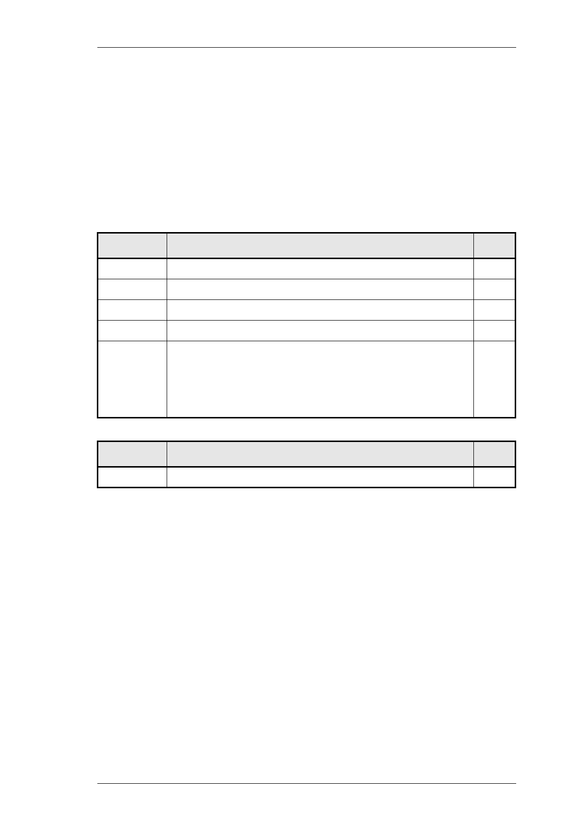
2.1 Introduction
Figure 2.1 High Level Block Diagram
The T889 comprises a three stage RF power amplifier with extensive control circuitry.
The final stage is composed of four transistors (Q3, Q4, Q5 & Q6) whose outputs are
combined to provide the rated output power.
The configuration of each of the main circuit blocks may be seen on a functional level in
Figure 2.1.
2.2 RF Circuitry
The driver stage of the T889 consists of a two stage transistor amplifier (Q1, Q2) which
delivers a minimum of 40W. This signal is split via three 3dB couplers (L13, L14 & L15)
and used to drive the four final amplifiers (Q3, Q4, Q5 & Q6). These outputs are recom-
bined by L40, L41 & L42 and passed to the antenna socket via the directional coupler
and low pass filter.
The directional coupler senses forward and reflected power, which is rectified (D1, D2)
and passed to the control circuitry for metering, alarm and power control purposes.
Power control is via a series pass transistor (Q16), which controls the supply voltage on
the collector of the driver transistor (Q1).
RF Out
Q1 Q2
Pad
RF In LPF
4W 40W
Q3
Q4
Q5
Q6
30W
30W
30W
30W
60W
60W
120W 100W
Power
Control Vsupply
Q16
L40L13
L15 L42
L14 L41
Directional
Coupler
2.4 Circuit Operation M889-00
02/10/95 Copyright TEL
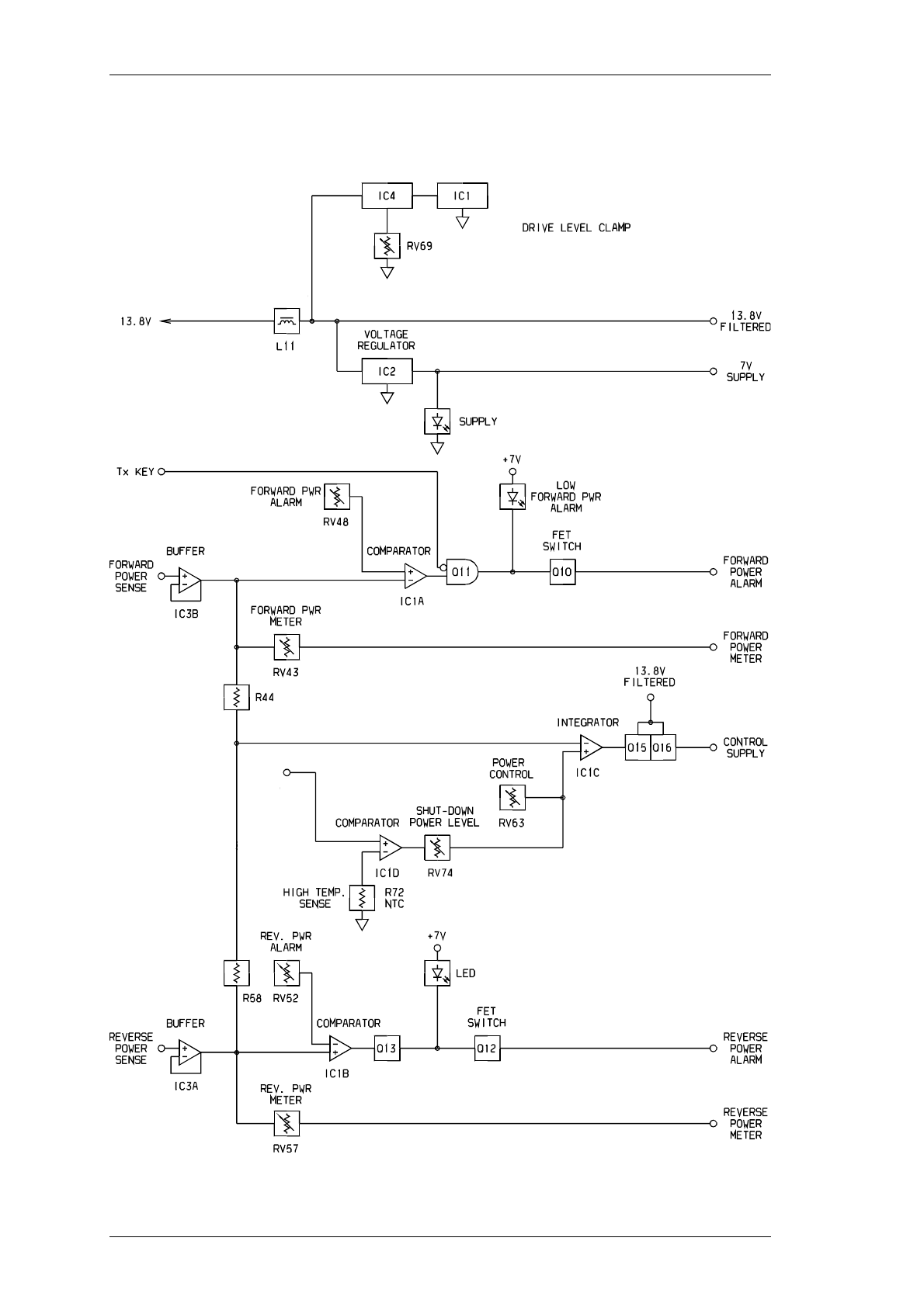
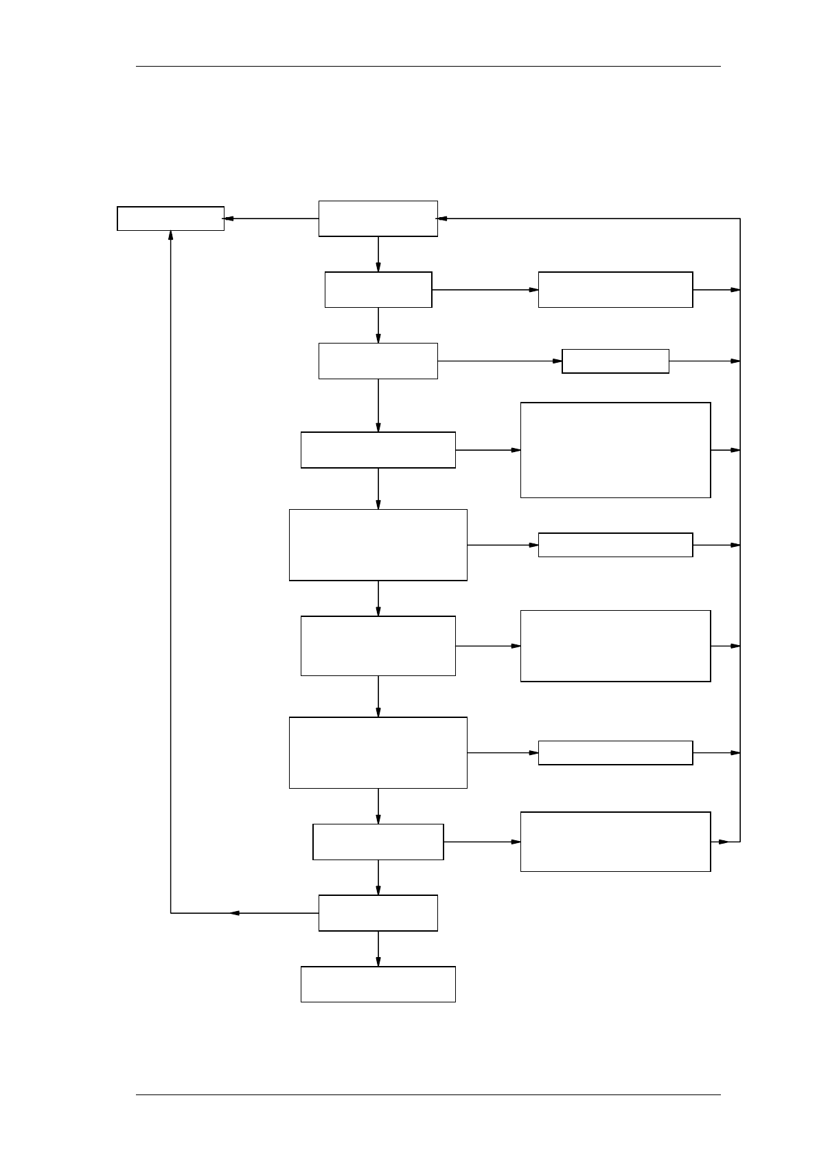
2.3 Control Circuitry
Figure 2.2 Control Circuitry Block Diagram
REF

M889-00 Circuit Operation 2.5
Copyright TEL 02/10/95
2.3.1 Power Control
The DC voltages from the directional coupler representing forward and reflected power
are buffered by the two voltage followers, IC3 pins 1, 2 & 3 and pins 5, 6 & 7. Their out-
puts are summed at an integrator (IC1 pins 8, 9 & 10), which drives the series pass con-
trol element (Q16).
Forward and reflected power are summed so that, under high output VSWR, the power
control turns the PA down. This is because the control loop adjusts for the same DC
voltage from the directional coupler that would have been present if there were no
reflected power.
2.3.2 Driver Power Level
The maximum output power of the T889 can be limited by placing a ceiling on the
driver output power level using RV69 (accessible through the side cover). For example,
if RV69 is set for a maximum output power of 50W, the range of adjustment using RV63
(front panel power adjust) will be 20 to 50W.
2.3.3 Thermal Protection
At excessively high temperatures, the output power will automatically reduce to a pre-
set level (set by RV74), thus preventing the PA from overheating.
A thermistor controlled voltage divider (R68, R72) applies a voltage to a comparator
with hysteresis (IC1 pins 12, 13 & 14).
The output current from the comparator is summed into the power control network via
RV74 so that the power level to which the PA must turn down may be set.
2.3.4 Forward And Reverse Power Alarms
If forward power drops below, or reverse power rises above, presettable limits, alarms
may be triggered.
The alarm outputs are open drain configuration and are low under normal conditions
(i.e. forward and reverse power levels are normal).
IC1 pins 1, 2 & 3 and pins 5, 6 & 7 form comparators with thresholds adjusted via RV48
and RV52 respectively. The inputs are from the forward and reverse power signals from
the directional coupler, buffered by IC3 pins 1, 2 & 3 and pins 5, 6 & 7. Thus, the power
levels at which the forward and reverse power alarms are triggered are defined by RV48
and RV52 respectively.
2.6 Circuit Operation M889-00
02/10/95 Copyright TEL
2.3.5 Forward And Reverse Power Metering
Forward and reverse power signals from the two IC3 buffers are available for metering
purposes. The output currents are adjustable via RV43 (forward power) and RV57
(reverse power).
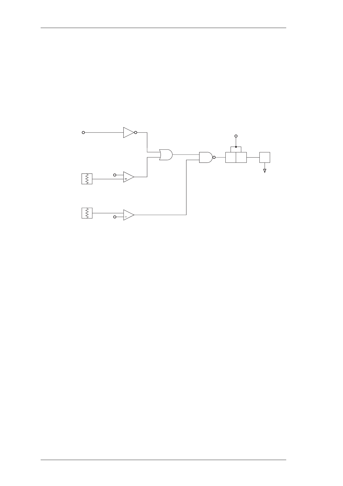
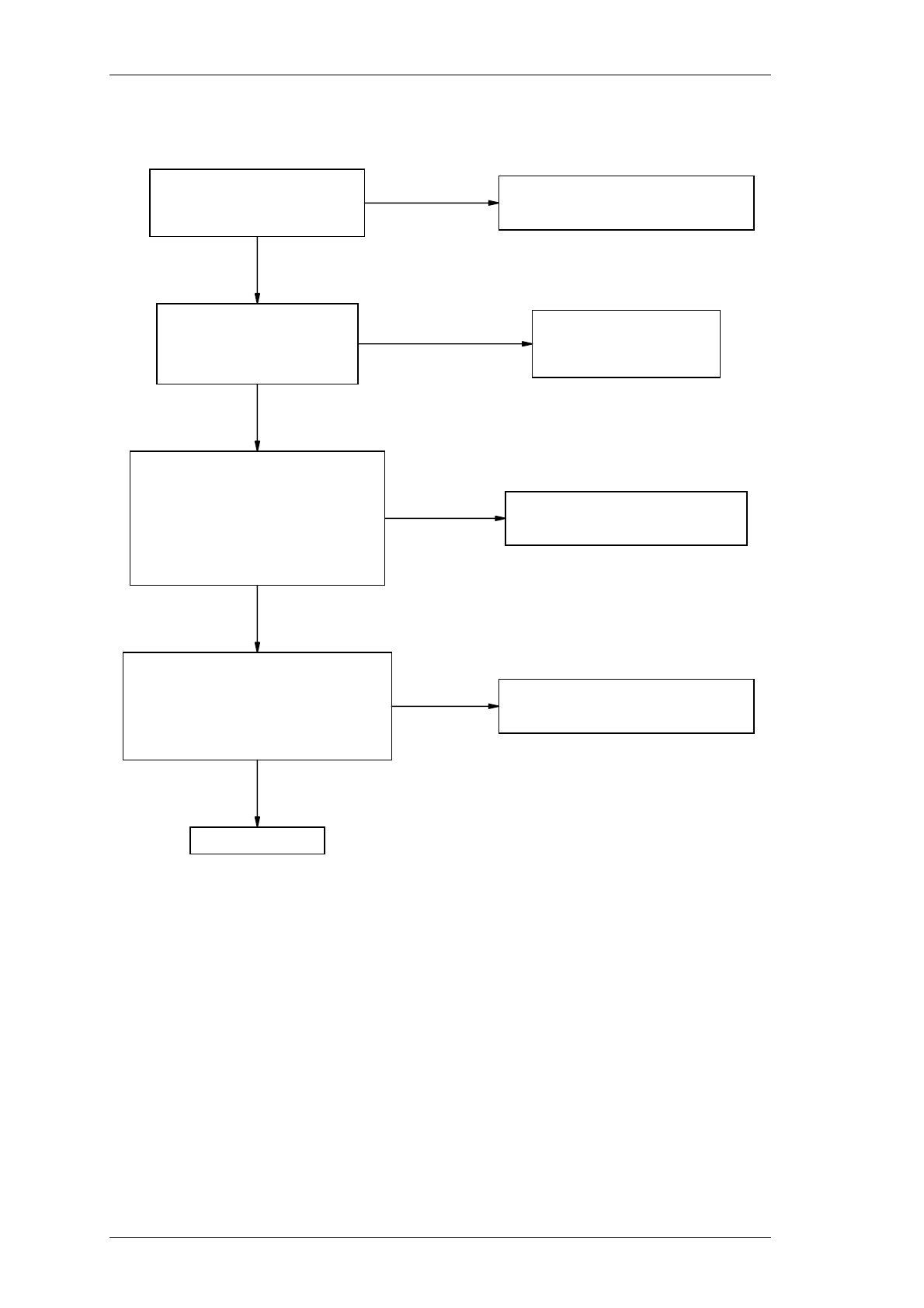
2.3.6 Fan Control Circuitry
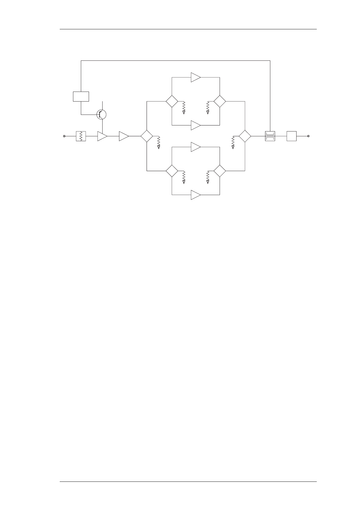
Figure 2.3 Fan Control Logic Diagram
Comparator IC3 pins 8, 9 & 10 are set to trigger at heatsink temperatures greater than
+70°C, and pins 12, 13 & 14 at temperatures greater than -10°C.
A logic AND function is applied to the comparator outputs by Q20 and Q21, thereby
turning on the fan unconditionally (via Q17 and Q18) if the heatsink temperature
exceeds +70°C.
A logic OR function is applied to comparator IC3 pins 8, 9 & 10 and Tx KEY signals,
thereby turning on the fan when the transmitter is keyed and the temperature is
between -10°C and +70°C.
If the temperature drops below -10°C, Q21 is turned off, preventing either Q19 or Q20
from activating the fan.
Q17 Q18 Fan
Ref
+
High Temp.
Sense
Comparator
IC3C
R72
Ref
+
Low Temp.
Sense
Comparator
IC3D
R116
NTC
NTC
Tx Key
Invert
Q19 OR
Q20,
R106, R107
NAND
Q20, Q21,
R119, R120 Fan Driver
13.8V
Filtered

M889-00 Introduction To Servicing 3.1
Copyright TEL 02/10/95
3 Introduction To Servicing
This section provides some general and advisory information on servicing procedures.
The following topics are covered in this section.
Section Title Page
3.1
3.1.1
3.1.2
3.1.3
General
Caution: CMOS Devices
Caution: Aerial Load
Caution: Beryllium Oxide & Power Transistors
3.3
3.3
3.3
3.4
3.2
3.2.1
3.2.2
3.2.3
3.2.4
Mechanical
Pozidriv Recess Head Screws
UNC Thread Screws
Screw Torques
Disassembly/Reassembly
3.5
3.5
3.5
3.5
3.5
3.3
3.3.1
3.3.1.1
3.3.1.2
3.3.2
Component Replacement
Leaded Components
Desoldering Iron Method
Component Cutting Method
Surface Mount Devices
3.6
3.6
3.6
3.6
3.7
3.4
3.4.1
3.4.1.1
3.4.1.2
3.4.2
To Replace PA Transistors
Capacitor /Transistor Spacing
Q1 (2SC2933 Pre-Driver)
Q2, Q3, Q4, Q5 & Q6 (SD1414)
Replacement Procedure
3.8
3.8
3.8
3.8
3.8
3.5 To Remove The PCB From The Heatsink 3.10
3.6 To Remove Cased Mica Capacitors 3.10
Figure Title Page
3.1 Typical Anti-static Bench Set-up 3.3
3.2 Typical Transistor/Capacitor Spacing (Q1 & Q2 Shown) 3.9

3.2 Introduction To Servicing M889-00
02/10/95 Copyright TEL
M889-00 Introduction To Servicing 3.3
Copyright TEL 02/10/95
3.1 General
If you require further information about the T889 or this manual, contact your nearest
authorised Tait Dealer or Service Centre. Further assistance may be obtained from the
Customer Support Group, Radio Infrastructure Division, Tait Electronics Ltd, Christch-
urch, New Zealand.
When requesting this information, please quote the equipment type number (e.g.
T889-10) and serial number. In the case of the service manual quote the Tait Internal
Part Number (IPN), e.g. M889-00-100, and for circuit diagrams quote the “Title”, “IPN”
and “Issue”.
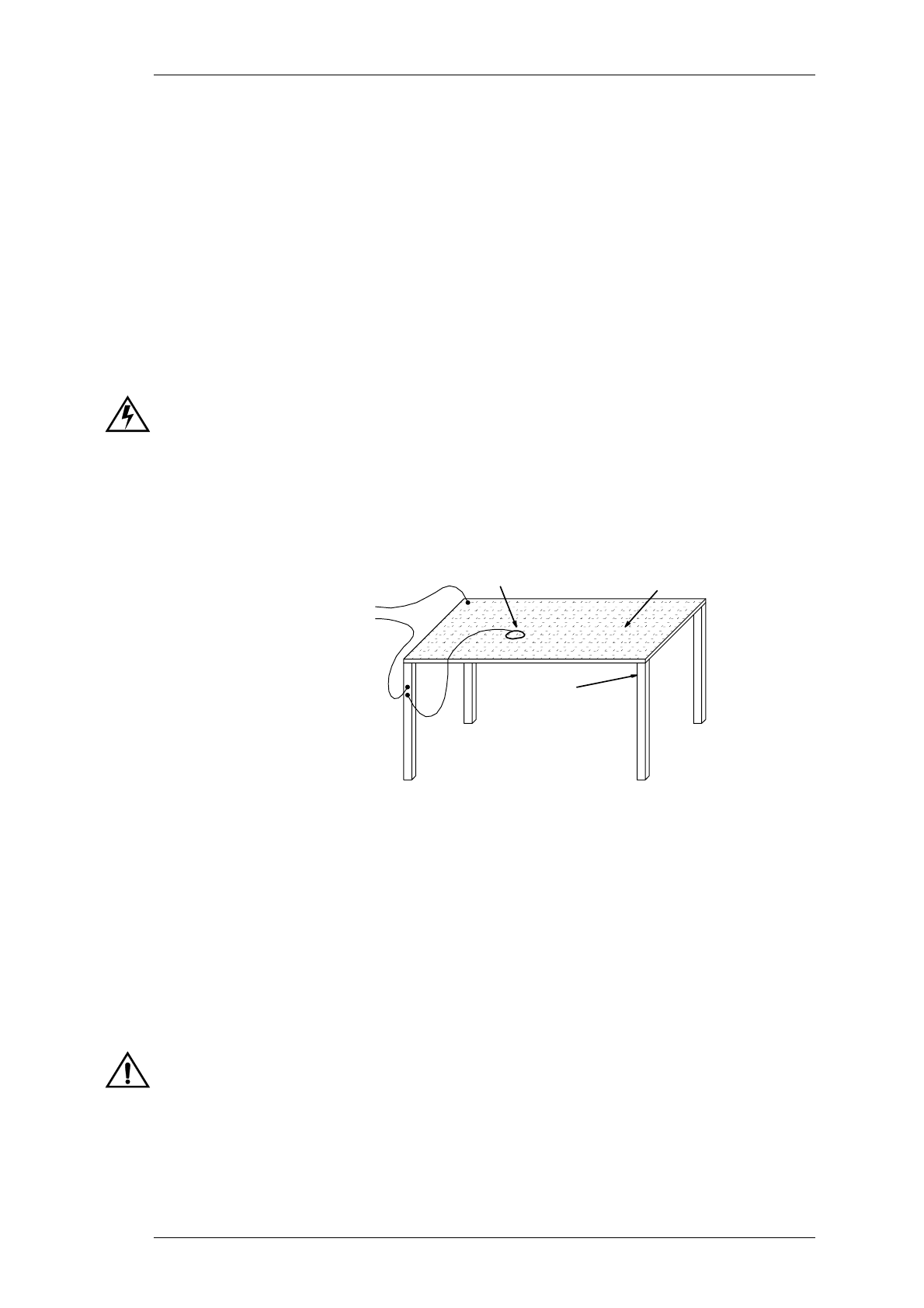
3.1.1 Caution: CMOS Devices
This equipment contains CMOS Devices which are susceptible to damage from static
charges. Care when handling these devices is essential. For correct handling proce-
dures refer to the manufacturers' data books, e.g. Philips data books covering CMOS
devices, or Motorola CMOS data books, Section 5 “Handling”, etc.
Figure 3.1 Typical Anti-static Bench Set-up
An anti-static bench kit (refer to Figure 3.1) is available from Tait Electronics Ltd under
the usual consumable goods ordering system. The kit is held in stock under IPN
937-00000-34 and contains:
1 conductive rubber bench mat
1 earth lead to connect the mat to ground (c/w 1M series resistor)
1 wrist strap
information leaflet.
3.1.2 Caution: Aerial Load
The equipment has been designed to operate safely under a wide range of aerial loading
conditions. However, it is strongly recommended that the transmitter should not be
operated in the absence of a suitable load. Failure to observe this warning may result in
damage to the transmitter output power stage.
conductive rubber
bench mat
metal frame
to building earth
(not mains earth)
via 1M series resistor
conductive
wrist strap

3.4 Introduction To Servicing M889-00
02/10/95 Copyright TEL
3.1.3 Caution: Beryllium Oxide & Power Transistors
The RF power transistors in current use all contain some beryllium oxide. This sub-
stance, while perfectly harmless in its normal solid form, can become a severe health
hazard when it has been reduced to dust. For this reason the RF power transistors
should not be broken open, mutilated, filed, machined, or physically damaged in any
way that can produce dust particles.

M889-00 Introduction To Servicing 3.5
Copyright TEL 02/10/95
3.2 Mechanical
3.2.1 Pozidriv Recess Head Screws
Pozidriv recess head screws are the preferred standard on all Tait manufactured equip-
ment. The very real advantages of this type of screw will not be realised unless the cor-
rect screwdrivers are used by servicing personnel.
3.2.2 UNC Thread Screws
All black finish Pozidriv screws used in the T889 are 4-40 UNC thread and cannot be
interchanged with M3 screws. Note that different lengths are used in different applica-
tions.
3.2.3 Screw Torques
It is important to tighten the cover and power transistor securing screws to the correct
torque to ensure that the T889 maintains its specified performance.
We recommend the following torque settings:
cover screws .. 6lb-in./0.7Nm
power transistors .. 6lb-in./0.7Nm
3.2.4 Disassembly/Reassembly
The power output level setting procedures should be carried out with the cover on.

3.6 Introduction To Servicing M889-00
02/10/95 Copyright TEL
3.3 Component Replacement
3.3.1 Leaded Components
Whenever components are removed from or fitted to the PCB, care must be taken to
avoid damage to the track. The two satisfactory methods of removing components from
PTH PCBs are detailed below.
Note: The first method requires the use of a desoldering station, e.g. Philips SBC
314 or Pace MBT-100E.
3.3.1.1 Desoldering Iron Method
Place the tip over the lead and, as the solder starts to melt, move the tip in a circu-
lar motion.
Start the suction and continue the movement until 3 or 4 circles have been com-
pleted.
Remove the tip while continuing suction to ensure that all solder is removed from
the joint, then stop the suction.
Before pulling the lead out, ensure it is not stuck to the plating.
If the lead is still not free, resolder the joint and try again.
Note: The desoldering iron does not usually have enough heat to desolder leads
from the ground plane. Additional heat may be applied by holding a sol-
dering iron on the tip of the desoldering iron (this may require some addi-
tional help).
3.3.1.2 Component Cutting Method
Cut the leads on the component side of the PCB.
Heat the solder joint sufficiently to allow easy removal of the lead by drawing it
out from the component side: do not use undue force.
Fill the hole with solder and then clear with solderwick.

M889-00 Introduction To Servicing 3.7
Copyright TEL 02/10/95
3.3.2 Surface Mount Devices
Caution: Surface mount devices (SMD's) require special storage, handling,
removal and replacement techniques. This equipment should be serv-
iced only by an approved Tait Dealer or Service Centre equipped with
the necessary facilities. Repairs attempted with incorrect equipment or
by untrained personnel may result in permanent damage. If in doubt,
contact Tait Electronics Ltd or your nearest Tait Branch or Subsidiary.

3.8 Introduction To Servicing M889-00
02/10/95 Copyright TEL
3.4 To Replace PA Transistors
Caution: As the location of certain components in the PA is critical to perform-
ance, it is important that any components removed or disturbed are
refitted in EXACTLY the same position.
Caution: Do not solder the tabs before torquing down otherwise the device may
be broken.
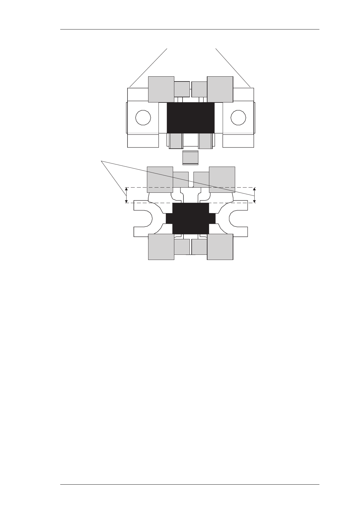
3.4.1 Capacitor /Transistor Spacing
Refer to Figure 3.2.
3.4.1.1 Q1 (2SC2933 Pre-Driver)
Before attempting to remove Q1, measure the distance between the capacitors
labelled “c” and the transistor body (measurement “a”) so that the capacitors can
be replaced in exactly the same position.
Note: Be sure to measure between the transistor body and the tabs (not the body)
of the capacitors.
Position the capacitors labelled “b” hard up against the transistor body.
3.4.1.2 Q2, Q3, Q4, Q5 & Q6 (SD1414)
Position all capacitors labelled “b” hard up against the transistor body.
3.4.2 Replacement Procedure
Desolder the tabs (and grounding clips if an SD1414) by heating with a soldering
iron and lifting away from the PCB with a thin stainless steel spike, or screw-
driver.
Unscrew the transistor and remove the device.
Smear the face of the replacement device with heatsink compound and tighten it
securely (torque setting 6lb-in./0.7Nm) to the heatsink. If you are replacing an
SD1414, remember to fit new grounding clips.
Solder the tabs.
Replace each capacitor as instructed in Section 3.4.1.
M889-00 Introduction To Servicing 3.9
Copyright TEL 02/10/95
Figure 3.2 Typical Transistor/Capacitor Spacing (Q1 & Q2 Shown)
Grounding Clips
b
bb
bb
cc
b
measurement a
Q1
Q2

3.10 Introduction To Servicing M889-00
02/10/95 Copyright TEL
3.5 To Remove The PCB From The Heatsink
Most components are soldered topside only, but in some cases access to the underside of
the PCB is necessary.
Remove the D-range connector.
Disconnect the power feed to the fan.
Remove the 13 PCB retaining screws (2 are hidden beneath the harmonic filter
shield).
Remove the transistor mounting screws.
Remove the mounting screws for the TO-220 devices:
R6, R7, R9, R16, R17, R17a and R18.
Remove the retaining screws for the wireline couplers (L13, L14, L15, L40, L41 and
L42).
Remove the output 50 ohm coaxial connector by unscrewing it from the heatsink
casting and desoldering it from the PCB.
Disconnect the input 50 ohm coaxial cable by unplugging it at the PCB.
Disconnect the battery positive and negative feed wires from the PCB.
Disconnect the alarm and metering wires from the PCB.
Lift the PCB gently from the heatsink to gain access to the underside of the PCB.
Caution: Do not operate the PA with the PCB detached as the heatsink is used
for earthing and for the dissipation of heat generated within the tran-
sistors.
To replace the PCB, reverse the order of removal, taking care that the wiring is cor-
rectly routed and is not subjected to 'pinching'.
3.6 To Remove Cased Mica Capacitors
Cased mica capacitors can be removed by heating the top with a heavy-duty soldering
iron and gently lifting the capacitor off the PCB with a solder-resistant spike or equiva-
lent.

M889-00 Initial Tuning & Adjustment 4.1
Copyright TEL 02/10/95
4 Initial Tuning & Adjustment
The following section describes the initial set-up procedures, including alarm adjust-
ment and power meter calibration.
The following topics are covered in this section.
Section Title Page
4.1 Initial Connections 4.3
4.2 RF Alignment 4.3
4.3 High Temperature Shutdown Power Level 4.3
4.4 Low Forward Power Alarm 4.3
4.5 High Reverse Power Alarm 4.4
4.6 Remote Forward Power Meter Calibration 4.4
4.7 Remote Reverse Power Meter Calibration 4.4

4.2 Initial Tuning & Adjustment M889-00
02/10/95 Copyright TEL

M889-00 Initial Tuning & Adjustment 4.3
Copyright TEL 02/10/95
4.1 Initial Connections
Connect the PA to a power supply, an output RF load and a power meter as
detailed below:
power supply rating >30A
RF load >150W.
Provide a keyed RF drive at the required frequency.
Connect the drive source key line to pin 12 of the external connector.
Set RV69 (temperature shutdown) fully anticlockwise to avoid RF power cycling
between the levels as set by RV63 and RV74.
4.2 RF Alignment
Set RV63 (power control) fully clockwise.
Key on the drive source (the power output should exceed 100W).
Adjust RV69 (driver power level) until the output power drops to 100W.
Adjust RV63 to reduce the power output to the required level (e.g. 90W).
4.3 High Temperature Shutdown Power Level
Set RV63 (power control) to the required output power.
Earth pin 12 of IC1 (the pad at NTC R72 is convenient).
Adjust RV74 (shutdown power level) for an output power of 20W.
Remove the earth from pin 12 of IC1.
4.4 Low Forward Power Alarm
Set RV63 (power control) to the output power at which the alarm is required to
activate.
Adjust RV48 (forward power alarm) until the front panel LED just lights.
Reset RV63 to the required output power.
Note: Remote indication is available at D-range pin 3.

4.4 Initial Tuning & Adjustment M889-00
02/10/95 Copyright TEL
4.5 High Reverse Power Alarm
Set RV63 to the required output power.
Connect a known mismatch of the required value to the PA output.
Apply RF drive and Tx key.
Adjust RV52 (reverse power alarm) so that the front panel high reverse power
LED just lights.
Example: A VSWR of 3:1 can be simulated by connecting an unterminated 150W
3dB pad to the PA output. This will result in a return loss of 6dB.
Note: Remote indication is available at D-range pin 4.
4.6 Remote Forward Power Meter Calibration
If a remote meter is connected, adjust RV43 (forward power meter) for the remote
reading to agree with the RF power meter reading.
4.7 Remote Reverse Power Meter Calibration
If a remote meter is connected, connect a 50 ohm 3dB pad (with the output open
circuit) to the PA output.
Apply RF drive and Tx key.
Adjust RV57 (reverse power meter) for a quarter of the forward power reading.
M889-00 Fault Finding 5.1
Copyright TEL 02/10/95
5 Fault Finding
The following test procedures and fault finding flow charts may be used to help locate a
hardware problem, however they are by no means a complete fault finding procedure.
If the fault still exists after having progressed through them in a logical manner, contact
your nearest authorised Tait Dealer or Service Centre. Further assistance may be
obtained from the Customer Support Group, Radio Infrastructure Division, Tait Elec-
tronics Ltd, Christchurch, New Zealand.
The following topics are covered in this section.
Section Title Page
5.1 Visual Checks 5.3
5.2 Component Checks 5.3
5.3 DC Checks 5.3
5.4 RF Checks 5.4
5.5
5.5.1
5.5.2
5.5.3
Fault Finding Charts
PA
Power Control
Fan Control Circuitry
5.7
5.7
5.8
5.9
Figure Title Page
5.1 Positioning Of Test Leads For Q1-Q6 5.6

5.2 Fault Finding M889-00
02/10/95 Copyright TEL

M889-00 Fault Finding 5.3
Copyright TEL 02/10/95
5.1 Visual Checks
Remove the cover from the T889 and inspect the PCB for damaged or broken com-
ponents, paying particular attention to the surface mounted devices (SMD's).
Check for defective solder joints. If repair or replacement is considered necessary,
refer to Sections 3.3, 3.4, 3.5 and 3.6.
5.2 Component Checks
If a transistor is suspected of faulty operation, an indication of its performance can be
assessed by measuring the forward and reverse resistance of the junctions. First make
sure that the transistor is not shunted by some circuit resistance (unless the device is
completely desoldered). A 20k ohm/V or better multimeter should be used for taking
the measurements, using only the medium or low resistance ranges.
The collector current drawn by multi-junction transistors is a further guide to their per-
formance.
If an IC is suspect, the most reliable check is to measure the DC operating voltages. Due
to the catastrophic nature of most IC failures, the pin voltages will usually be markedly
different from the recommended values in the presence of a fault. The recommended
values can be obtained from either the circuit diagram or the component data catalogue.
5.3 DC Checks
Check that +13.8V is present on the collectors of Q2, Q3, Q4, Q5 and Q6. Make
this measurement when the transmitter is not keyed.
Check that approximately 8-13.8V is present on the collector of Q1 (the level is
dependent on RV69 being set to maximum).
Check that +13.8V is present at pin 4 of IC3.
Check that approximately +12V is present at pin 4 of IC1 (the level is dependent
on RV69 being set to maximum).
Check that +7.0V is present at the output of regulator IC2.

5.4 Fault Finding M889-00
02/10/95 Copyright TEL
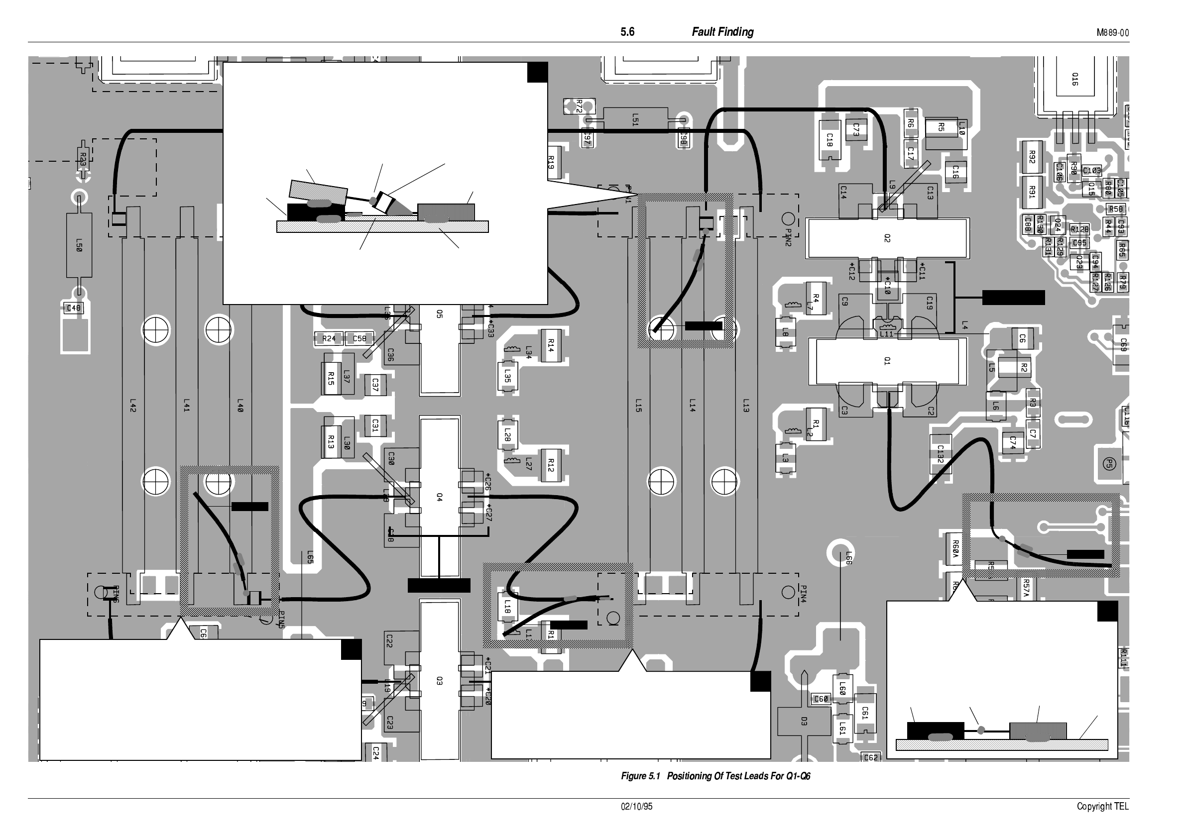
5.4 RF Checks
The PA Fault Finding Chart (Section 5.5.1) provides a systematic approach for locating a
fault in the RF circuitry. Use this chart in conjunction with Figure 5.1, which shows the
locations of the 50Ω input and output test points for RF transistors Q1-Q6.
Note 1: Always test individual PA stages at the 50Ω test points, located at the ends
of the semi-rigid transmission lines furthest away from the RF transistors.
Note 2: Always test Q1 and Q2 as a pair.
Note 3: Use 50Ω semi-rigid coax for the flying test leads.
For problems with the power control circuitry, refer to the Power Control Fault Finding
Chart (Section 5.5.2).
Transistor Input Transmission Line Output Transmission Line
Q1-Q2 L1 L12
Q3 L16 L22
Q4 L26 L32
Q5 L33 L39
Q6 L43 L49

M889-00 Fault Finding 5.5
Copyright TEL 02/10/95
replace A4 pages 5.5/5.6 with A3 pages
5.5/5.6, file name 88900_5a.100

5.6 Fault Finding M889-00
02/10/95 Copyright TEL
replace A4 pages 5.5/5.6 with A3 pages
5.5/5.6, file name 88900_5a.100
M889-00 Fault Finding 5.7
Copyright TEL 02/10/95
5.5 Fault Finding Charts
5.5.1 PA
Is maximum power
>90W @ 800-870MHz?
Are RV69 & RV63
fully clockwise?
Is the drive from
the exciter 4W?
Rotate clockwise:
RV63 first, RV69 second.
Set drive to 4W.
RF circuitry OK.
Replace splitter hybrid.
Check collectors >13V.
Check for shorts around
transistor caps.
Check transistor junction
resistance (see Section 5.2).
Is maximum power
>90W @ 800-870MHz?
Return PA to your local
Tait service centre.
Replace combiner hybrid.
Check components in LPF.
Check output N-type connector
for short or wear.
Replace parts as necessary.
N
N
N
Y
Y
Y
Y
N
N
Y
Y
N
Y
N
N
Y
Y
Is Q2 output >40W?
(see Figure 5.1, A & B) N
Check the condition of
splitter hybrids L13, L14 & L15.
Are there any shorts
between the splitter wires
or broken wires?
Q3, Q4, Q5 & Q6
outputs each >30W?
(test each individually
as per Figure 5.1, C & D)
Check the condition of
combiner hybrids L40, L41 & L42.
Are there any shorts
between the combiner wires
or broken wires?
Are R17 & R17A hot to
touch when PA keyed?
Check Q1 collector >13V.
Check Q2 collector 5-14V.
Check for shorts around
transistor caps C2, 3, 9,
19, 10, 11, 12, 13 & 14.
Check transistor junction
resistance (see Section 5.2).
5.8 Fault Finding M889-00
02/10/95 Copyright TEL
5.5.2 Power Control
Use RV63 to adjust
output power to 60W.
Adjust RV48 until forward
power LED is just lit.
Power control OK.
N
N
N
Y
Y
Y
Y
Ensure RV69 is fully clockwise.
Check sense voltages from
directional coupler on IC3 pins 1 & 7.
With the 3dB pad connected to
the PA, adjust RV52 until the
high reverse power LED is just lit.
Short R72 to ground with spike, etc.,
while adjusting RV74 until PA
output power is set to 35W.
Does high reverse power alarm
LED light when PA operated into
a mismatch of 3:1 or worse?
To test, connect an unterminated
3dB pad to the PA output,
thereby setting up a 3:1 mismatch.
High Reverse Power Alarm Check
Does the output power reduce to
35W at high operating temperatures?
To test, heat R72 with the tip of a
soldering iron.
Over-Temperature Shutdown Check
Does low forward power alarm
LED light when output power
reduced to 60W using RV63?
Low Forward Power Alarm Check
Does output power adjust over
the range 20-100W using RV63?
RF Power Level Control Check
N
M889-00 Fault Finding 5.9
Copyright TEL 02/10/95
5.5.3 Fan Control Circuitry
Key transmitter.
Does fan run at
room temperature?
Spray "freeze" on R116
or short R113.
Does the low temperature
inhibit circuit stop the fan?
Spray "freeze" on R116
OR short R113.
Check IC3 pin 14 >11V.
Check Q21 & Q20.
N
N
Y
Y
Check Q20 & Q21 collector
voltages. Check Q17 & Q18.
Check IC3 pin 14 <1V.
Check Q19.
Check Tx-key is low (at ground).
Do not key
transmitter.
Does high temperature control
circuit activate fan?
Heat R72 with tip
of soldering iron.
Check IC3 pin 8 >11V.
Check Q21 & Q20.
Fan control OK.
Heat R72 to >70°C with
tip of soldering iron.
N
Y

5.10 Fault Finding M889-00
02/10/95 Copyright TEL

L46
C97 C98
L19
L29
L96
C59
L22 L16
L32 L26
L1
L49 L43L12
L39 L33
C45 C38
C15
C32
C25
Output Test Lead - Q1 & Q2
1. Desolder C15 and resolder on edge as shown.
2. Remove the wireline clamping plate and solder the test lead outer core to the outer
core of the wireline (L14 shown).
3. Solder the inner core of the test lead to the raised end of C15.
4. To test Q1 & Q2, provide 2.5-3W drive power to Q1 through the input test lead. While
testing, ensure that the output test lead on Q2 is terminated at all times into a good
50Ω RF load.
main PCB
Teflon PCB
L14 L12
C15 (DC blocking capacitor)
output test lead
(transmission line)
(wireline)
(to wattmeter, analyser etc.) 50Ω test point
Input Test Lead - Q1 & Q2
1. Desolder the inner core of L1 and lift off its pad.
2. Solder the test lead outer core to the earth plane (remove
the resist first).
3. Solder the inner cores of L1 and the test lead together off
the PCB.
main PCB
L1 input test lead
50Ω test point
Output Test Lead - Q3-Q6 (Q4 Shown)
Refer to drawing B above.
1. Desolder the appropriate DC blocking capacitor and resolder on edge.
2. Remove the wireline clamping plate and solder the test lead outer core to the outer
core of the wireline.
3. Solder the inner core of the test lead to the raised end of the DC blocking capacitor.
4. To test, drive the transistor with approx. 10W over the range 800-870MHz and expect
a minimum output of 30W.
Input Test Lead - Q3-Q6 (Q4 Shown)
1. Desolder the appropriate transmission line inner core and lift off its pad.
2. Solder the test lead outer core to the transmission line outer core.
3. Solder the inner cores of the transmission line and test lead together off
the PCB.
not 50Ω
not 50Ω
test lead
test lead
test lead
test lead
A
B
C
D
M889-00 Installation 6.1
Copyright TEL 02/10/95
6 Installation
The following section gives a brief description of the basic rack mounting and wiring
procedures.
The following topics are covered in this section.
Section Title Page
6.1 Rack Mounting 6.3
6.2 Rack Wiring 6.5
6.3 Power Supply 6.5
Figure Title Page
6.1 Guide Rails 6.3
6.2 Chassis Connectors 6.3
6.3 Latched Position 6.4
6.4 D-Range Wiring - Rear View 6.5

6.2 Installation M889-00
02/10/95 Copyright TEL
M889-00 Installation 6.3
Copyright TEL 02/10/95
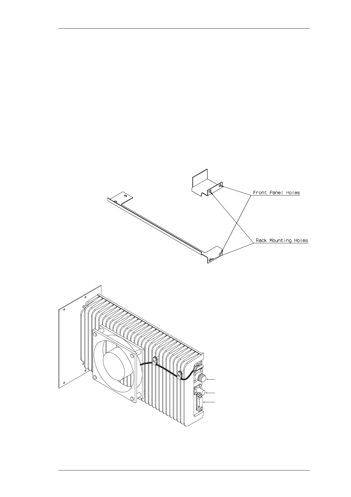
6.1 Rack Mounting
The T889 PA is designed for use in a standard 483mm rack frame using the supporting
guide rails supplied with the unit (refer to Figure 6.1).
The lower guide rail is located in the rack frame with three screws, two at the rear and
one at the front. The short upper guide rail is located with just one screw. The PA is
secured into the guide with two front panel mounting screws.
The RF input via the rear panel BNC connector should be connected to an adjacent T881
transmitter. The RF output is via the rear N-type connector, whilst all DC, audio and
control connections are via the D-range connector.
The guide rails will allow the PA to be latched in the extended position (refer to Figure
6.3).
Figure 6.1 Guide Rails
Figure 6.2 Chassis Connectors
N-Type Connector
BNC Connector
D-Range Connector
6.4 Installation M889-00
02/10/95 Copyright TEL
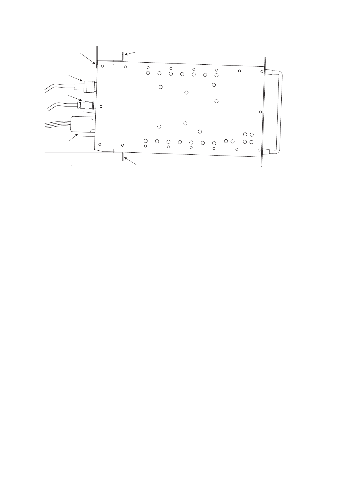
Figure 6.3 Latched Position
Stop
RF Output
Top Rail
RF Input
D-Range
Bottom Rail
M889-00 Installation 6.5
Copyright TEL 02/10/95
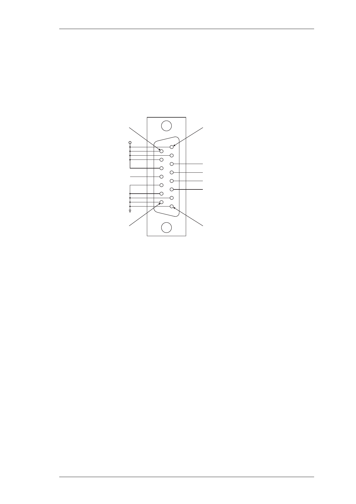
6.2 Rack Wiring
Wire the D-range connector as shown in Figure 6.4. Ensure that the cables are not sub-
jected to any stresses due to tight bends or incorrect lengths.
The RF coaxial cables to the BNC and N-type connectors should be free from acute
bends or twists. If access to the rear of the rack frame is restricted, the cables should be
long enough to permit full withdrawal of the chassis from the guide.
Figure 6.4 D-Range Wiring - Rear View
6.3 Power Supply
If a power supply other than an appropriate Tait model is used, ensure that it is capable
of providing enough current to drive the T800 system and is also free from excessive
ripple or noise.
Reverse Power Metering
Forward Power Metering
Reverse Power Alarm
Forward Power Alarm
Tx Key
+13.8V
Gnd
Pin 15 Pin 8
Pin 1Pin 9

6.6 Installation M889-00
02/10/95 Copyright TEL

M889-00 PCB Information 7.1.1
Copyright TEL 02/10/95
7 PCB Information
This section provides parts lists, a grid reference index, PCB layouts and circuit diagrams for the
T889 PA.
This section contains the following information.
Section Title IPN Page
7.1 Introduction 7.1.3
7.2 T889 PA PCB 220-01326-01 7.2.1

7.1.2 PCB Information M889-00
02/10/95 Copyright TEL

M889-00 PCB Information 7.1.3
Copyright TEL 02/10/95
7.1 Introduction
PCB Identification
All PCBs are identified by a unique 10 digit number, the last 2 digits of which define the issue status.
The issue status starts at 00 and increments through 01, 02, 03, etc. as the PCB is updated. Some
issue PCBs never reach full production status and are therefore not included in this manual. A let-
ter following the 10 digit IPN has no relevance in identifying the PCB for service purposes.
Parts Lists
The 10 digit numbers (000-00000-00) in this Parts List are “internal part numbers” (IPNs). Your
spare parts orders can be handled more efficiently if you quote the IPN and provide a brief descrip-
tion of the part.
The components listed in this parts list are divided into two main types: those with a circuit refer-
ence (e.g. C2, D1, R121, etc.) and those without (miscellaneous and mechanical).
Those with a circuit reference are grouped firstly by PCB, then by component type in numerical
order. Each component entry comprises three or four columns: the circuit reference, variant
number (if applicable), IPN and description. A number in the variant column indicates that this
component is fitted only to that variant.
The miscellaneous and mechanical section lists the variant and common parts in IPN order.
Grid Reference Index
To assist in locating components and labelled pads on the PCB layouts and circuit diagrams, a com-
ponent grid reference index has been provided. This index lists the components and pads in alpha-
betical order, along with the appropriate alphanumeric grid references.
The first digit in the circuit diagram reference is the sheet number, and the last two characters give
the location of the component on that sheet.
The first digit in the PCB layout reference is a “1” or “2”, indicating the top or bottom side layout
respectively, and the last two characters give the location of the component on that diagram.
Using CAD Circuit Diagrams
Reading a CAD circuit diagram is similar to reading a road map, in that both have an alphanumeric
border. The circuit diagrams in this manual use letters to represent the horizontal axis, and num-
bers for the vertical axis. These circuit diagram “grid references” are useful in following a circuit
that is spread over two or more sheets.
When a line representing part of the circuitry is discontinued, a reference will be given at the end of

7.1.4 PCB Information M889-00
02/10/95 Copyright TEL
the line to indicate where the rest of the circuitry is located. The first digit refers to the sheet number
(printed on the bottom right hand corner of the CAD diagram) and the last two characters refer to
the location on that sheet of the continuation of the circuit (e.g. 1-D4).
If more than one line is represented (indicated by a double thickness line), a dot with a reference
label will follow the route each individual line represents.

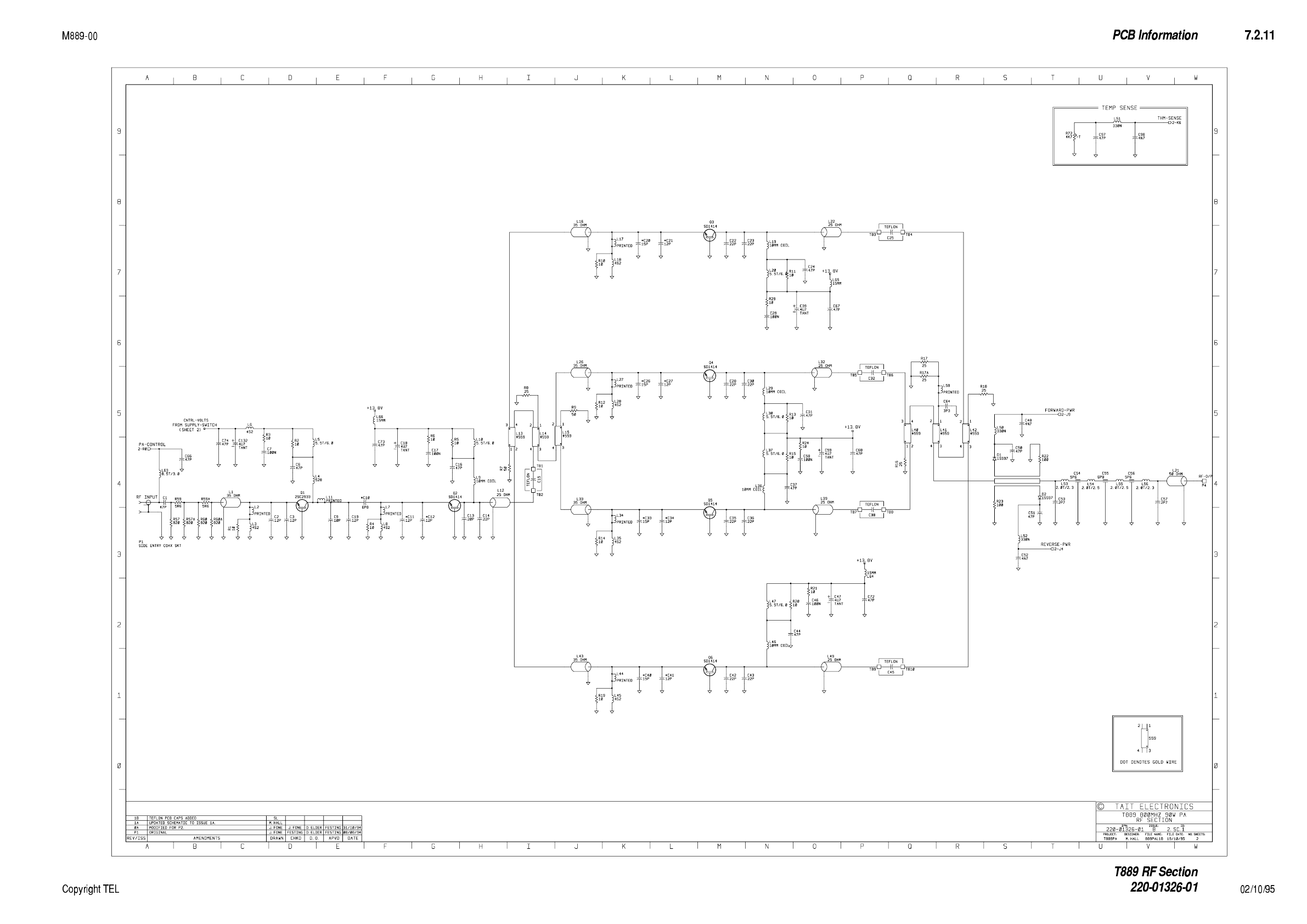
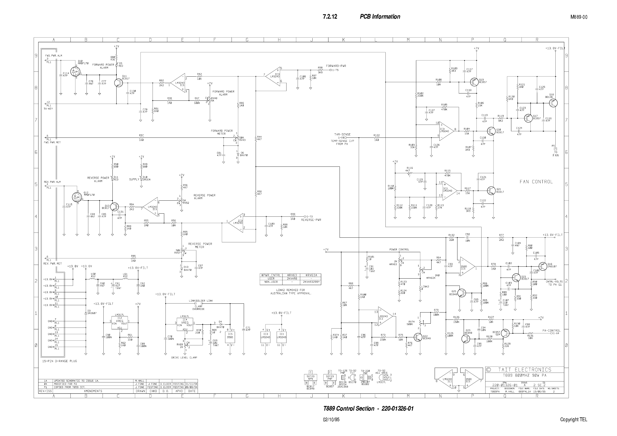
M889-00 PCB Information 7.2.1
Copyright TEL 02/10/95
7.2 T889 PA PCB
This section contains the following information.
IPN Section Page
220-01326-01 Parts List
Mechanical & Miscellaneous Parts
Grid Reference Index
PCB Layout - Bottom Side
PCB Layout - Top Side
RF Section Circuit Diagram
Control Section Circuit Diagram
7.2.2
7.2.5
7.2.7
7.2.9
7.2.10
7.2.11
7.2.12

7.2.2 PCB Information M889-00
02/10/95 Copyright TEL
T889 Parts List (IPN 220-01326-01)
How To Use This Parts List
The components listed in this parts list are divided into two main types: those with a circuit reference (e.g. C2, D1, R121, etc) and
those without (miscellaneous and mechanical).
Those with a circuit reference are grouped by component type in numerical order. Each component entry comprises three or four col-
umns: the circuit reference, variant number (if applicable), IPN and description. A number in the variant column indicates that this
component is fitted only to that variant.
The miscellaneous and mechanical section lists the variant and common parts in IPN order.
Parts List Amendments
Although shown in the parts list, PCB layout and circuit diagrams, R57A, R59A and R60A are not fitted (to increase the drive to Q1).
Ref Var IPN Description Ref Var IPN Description
C1 015-02470-03 CAP CER CHIP 47P 5% NPO 500V HIQ GRH111 2.
C2 029-02120-02 CAP MICA 5MM CASE 12P 5%
C3 029-02120-02 CAP MICA 5MM CASE 12P 5%
C6 015-02470-03 CAP CER CHIP 47P 5% NPO 500V HIQ GRH111 2.
C7 015-06100-08 CAP CER 1206 CHIP 100N 10% X7R 50V
C9 029-02100-02 CAP MICA 5MM CASE 10P 5%
C10 015-01680-02 CAP CER HIQ 1210 CHIP 6P8 5% NPO 200V
C11 015-02120-03 CAP CER CHIP 12P 5% 500V HIQ GRH111 2.8MM
C12 015-02120-03 CAP CER CHIP 12P 5% 500V HIQ GRH111 2.8MM
C13 029-02200-02 CAP MICA 5MM CASE 20P 5%
C14 029-02220-02 CAP MICA 5MM CASE 22P 5%
C15 015-02470-03 CAP CER CHIP 47P 5% NPO 500V HIQ GRH111 2
C16 015-02470-03 CAP CER CHIP 47P 5% NPO 500V HIQ GRH111 2
C17 015-06100-08 CAP CER 1206 CHIP 100N 10% X7R 50V
C18 014-07470-03 L) CAP TANT CHIP 4U7 25V +-20% 6X3.2X2.5M
C19 029-02120-02 CAP MICA 5MM CASE 12P 5%
C20 015-02150-03 CAP CER CHIP 15P 5% 500V HIQ GRH111 2.8MM
C21 015-02120-03 CAP CER CHIP 12P 5% 500V HIQ GRH111 2.8MM
C22 029-02220-02 CAP MICA 5MM CASE 22P 5%
C23 029-02220-02 CAP MICA 5MM CASE 22P 5%
C24 015-02470-03 CAP CER CHIP 47P 5% NPO 500V HIQ GRH111 2
C25 015-02470-03 CAP CER CHIP 47P 5% NPO 500V HIQ GRH111 2
C26 015-02150-03 CAP CER CHIP 15P 5% 500V HIQ GRH111 2.8MM
C27 015-02120-03 CAP CER CHIP 12P 5% 500V HIQ GRH111 2.8MM
C28 029-02220-02 CAP MICA 5MM CASE 22P 5%
C29 015-06100-08 CAP CER 1206 CHIP 100N 10% X7R 50V
C30 029-02220-02 CAP MICA 5MM CASE 22P 5%
C31 015-02470-03 CAP CER CHIP 47P 5% NPO 500V HIQ GRH111 2
C32 015-02470-03 CAP CER CHIP 47P 5% NPO 500V HIQ GRH111 2
C33 015-02150-03 CAP CER CHIP 15P 5% 500V HIQ GRH111 2.8MM
C34 015-02120-03 CAP CER CHIP 12P 5% 500V HIQ GRH111 2.8MM
C35 029-02220-02 CAP MICA 5MM CASE 22P 5%
C36 029-02220-02 CAP MICA 5MM CASE 22P 5%
C37 015-02470-03 CAP CER CHIP 47P 5% NPO 500V HIQ GRH111 2
C38 015-02470-03 CAP CER CHIP 47P 5% NPO 500V HIQ GRH111 2
C39 014-07470-03 L) CAP TANT CHIP 4U7 25V +-20% 6X3.2X2.5M
C40 015-02150-03 CAP CER CHIP 15P 5% 500V HIQ GRH111 2.8MM
C41 015-02120-03 CAP CER CHIP 12P 5% 500V HIQ GRH111 2.8MM
C42 029-02220-02 CAP MICA 5MM CASE 22P 5%
C43 029-02220-02 CAP MICA 5MM CASE 22P 5%
C44 015-02470-03 CAP CER CHIP 47P 5% NPO 500V HIQ GRH111 2
C45 015-02470-03 CAP CER CHIP 47P 5% NPO 500V HIQ GRH111 2
C46 015-06100-08 CAP CER 1206 CHIP 100N 10% X7R 50V
C47 014-07470-03 L) CAP TANT CHIP 4U7 25V +-20% 6X3.2X2.5M
C48 015-24470-08 CAP CER 0805 CHIP 4N7 10% X7R 50V
C50 015-22470-01 CAP CER 0805 CHIP 47P 5% NPO 50V
C51 015-22470-01 CAP CER 0805 CHIP 47P 5% NPO 50V
C52 015-24470-08 CAP CER 0805 CHIP 4N7 10% X7R 50V
C53 029-01270-02 CAP MICA 5MM CASE 2P7 +-0.25P
C54 029-01560-01 CAP MICA 10MM CASE 5P6 +-0.25P
C55 029-01680-01 CAP MICA 10MM CASE 6P8 5%
C56 029-01560-01 CAP MICA 10MM CASE 5P6 +-0.25P
C57 029-01270-02 CAP MICA 5MM CASE 2P7 +-0.25P
C58 015-06100-08 CAP CER 1206 CHIP 100N 10% X7R 50V
C59 014-07470-03 L) CAP TANT CHIP 4U7 25V +-20% 6X3.2X2.5M
C60 015-24470-08 CAP CER 0805 CHIP 4N7 10% X7R 50V
C61 014-07470-03 L) CAP TANT CHIP 4U7 25V +-20% 6X3.2X2.5M
C62 015-24100-08 CAP CER 0805 CHIP 1N 10% X7R 50V
C64 015-01330-06 CAP CER 1210 CHIP 3P3 NPO 500V GRM42-2
C65 015-22470-01 CAP CER 0805 CHIP 47P 5% NPO 50V
C66 015-22470-01 CAP CER 0805 CHIP 47P 5% NPO 50V
C67 015-02470-03 CAP CER CHIP 47P 5% NPO 500V HIQ GRH111 2
C68 015-02470-03 CAP CER CHIP 47P 5% NPO 500V HIQ GRH111 2
C69 014-08100-00 CAP TANT CHIP 10M 16VW +-20% 6X3.2X2.5MM
C70 015-06100-08 CAP CER 1206 CHIP 100N 10% X7R 50V
C71 015-22470-01 CAP CER 0805 CHIP 47P 5% NPO 50V
C72 015-02470-03 CAP CER CHIP 47P 5% NPO 500V HIQ GRH111 2
C73 015-02470-03 CAP CER CHIP 47P 5% NPO 500V HIQ GRH111 2
C74 015-02470-03 CAP CER CHIP 47P 5% NPO 500V HIQ GRH111 2
C76 015-24470-08 CAP CER 0805 CHIP 4N7 10% X7R 50V
C77 015-22470-01 CAP CER 0805 CHIP 47P 5% NPO 50V
C78 015-22470-01 CAP CER 0805 CHIP 47P 5% NPO 50V
C81 015-22470-01 CAP CER 0805 CHIP 47P 5% NPO 50V
C84 015-24470-08 CAP CER 0805 CHIP 4N7 10% X7R 50V
C85 015-22470-01 CAP CER 0805 CHIP 47P 5% NPO 50V
C87 015-22470-01 CAP CER 0805 CHIP 47P 5% NPO 50V
C88 015-22470-01 CAP CER 0805 CHIP 47P 5% NPO 50V
C89 015-06100-08 CAP CER 1206 CHIP 100N 10% X7R 50V
C90 015-06100-08 CAP CER 1206 CHIP 100N 10% X7R 50V
C91 014-08100-00 CAP TANT CHIP 10M 16VW +-20% 6X3.2X2.5MM
C92 015-25100-08 CAP CER 0805 CHIP 10N 10% X7R 50V
C93 015-22470-01 CAP CER 0805 CHIP 47P 5% NPO 50V
C94 015-25100-08 CAP CER 0805 CHIP 10N 10% X7R 50V
C95 015-22470-01 CAP CER 0805 CHIP 47P 5% NPO 50V
C96 015-22470-01 CAP CER 0805 CHIP 47P 5% NPO 50V
C97 015-22470-01 CAP CER 0805 CHIP 47P 5% NPO 50V
C98 015-24470-08 CAP CER 0805 CHIP 4N7 10% X7R 50V
C99 015-22470-01 CAP CER 0805 CHIP 47P 5% NPO 50V
C102 015-22470-01 CAP CER 0805 CHIP 47P 5% NPO 50V
C103 015-22470-01 CAP CER 0805 CHIP 47P 5% NPO 50V
C104 015-24470-08 CAP CER 0805 CHIP 4N7 10% X7R 50V
C105 015-22470-01 CAP CER 0805 CHIP 47P 5% NPO 50V
C106 015-22470-01 CAP CER 0805 CHIP 47P 5% NPO 50V
C107 014-07100-02 CAP TANT CHIP 1U0 3.2 X 1.6MM 267 SERIES
C108 015-22470-01 CAP CER 0805 CHIP 47P 5% NPO 50V
C109 015-22470-01 CAP CER 0805 CHIP 47P 5% NPO 50V
C114 015-22470-01 CAP CER 0805 CHIP 47P 5% NPO 50V
C115 015-22470-01 CAP CER 0805 CHIP 47P 5% NPO 50V
C116 015-22470-01 CAP CER 0805 CHIP 47P 5% NPO 50V
C117 015-22470-01 CAP CER 0805 CHIP 47P 5% NPO 50V
C118 015-22470-01 CAP CER 0805 CHIP 47P 5% NPO 50V
C119 015-22470-01 CAP CER 0805 CHIP 47P 5% NPO 50V
C120 015-22470-01 CAP CER 0805 CHIP 47P 5% NPO 50V
C121 015-22470-01 CAP CER 0805 CHIP 47P 5% NPO 50V
C122 015-22470-01 CAP CER 0805 CHIP 47P 5% NPO 50V
C123 015-22470-01 CAP CER 0805 CHIP 47P 5% NPO 50V
C124 015-22470-01 CAP CER 0805 CHIP 47P 5% NPO 50V
C125 015-22470-01 CAP CER 0805 CHIP 47P 5% NPO 50V
C126 015-22470-01 CAP CER 0805 CHIP 47P 5% NPO 50V
C127 015-22470-01 CAP CER 0805 CHIP 47P 5% NPO 50V
C128 015-22470-01 CAP CER 0805 CHIP 47P 5% NPO 50V
C129 015-22470-01 CAP CER 0805 CHIP 47P 5% NPO 50V
C130 015-22470-01 CAP CER 0805 CHIP 47P 5% NPO 50V
C131 015-22470-01 CAP CER 0805 CHIP 47P 5% NPO 50V
C132 014-07470-03 L) CAP TANT CHIP 4U7 25V +-20% 6X3.2X2.5
D1 001-00013-45 (S) DIODE SCHOTTKY 1SS97/2
D2 001-00013-45 (S) DIODE SCHOTTKY 1SS97/2

M889-00 PCB Information 7.2.3
Copyright TEL 02/10/95
Ref Var IPN Description Ref Var IPN Description
D3 001-00011-60 (S) DIODE SR2607 6A/30V
D4 001-10000-70 (S) DIODE SMD BAV70 DUAL SWITCH SOT-23 CO
D6 001-10000-70 (S) DIODE SMD BAV70 DUAL SWITCH SOT-23 CO
D13 001-10000-70 (S) DIODE SMD BAV70 DUAL SWITCH SOT-23 CO
FTC 012-04100-05 CAP F/THRU 1N SUPPR FLTR STUD MTG
(fan circuit; mounted on heatsink)
IC1 002-10003-24 (S) IC SMD 324 QUAD OP AMP SO14
IC2 002-00014-62 (S) IC 317L 100MA REG 3 TERMINAL TO-92
IC3 002-10003-24 (S) IC SMD 324 QUAD OP AMP SO14
IC4 002-00014-62 (S) IC 317L 100MA REG 3 TERMINAL TO-92
IC5 002-10003-58 (S) IC SMD LM358 DUAL OP AMP
L1 051-00626-00 COAX 1/4 WAVE XFMR 35E HELI LEFT HAND
L3 065-10004-20 BEAD FE SMD CBD 4.6/3/3-4S2
L4 051-00005-28 COIL TAIT NO 528 HAIRPIN 17MM T550A
L5 052-08160-55 COIL A/W 5.5T/6.0MM HOR 0.8MM WIRE
L6 065-10004-20 BEAD FE SMD CBD 4.6/3/3-4S2
L8 065-10004-20 BEAD FE SMD CBD 4.6/3/3-4S2
L9 051-00005-60 IND HAIRPIN 10MM TALL T859
L10 052-08160-55 COIL A/W 5.5T/6.0MM HOR 0.8MM WIRE
L12 051-00623-00 COAX 1/4 WAVE XFMR 25E HAIR PIN
L13 051-00619-00 COUPLER WIRELINE 800MHZ (53MM JACKET ST
L14 051-00619-00 COUPLER WIRELINE 800MHZ (53MM JACKET ST
L15 051-00619-00 COUPLER WIRELINE 800MHZ (53MM JACKET ST
L16 051-00629-00 COAX 1/4 WAVE XFMR 35E HOCKEY STICK RIGH
L18 065-10004-20 BEAD FE SMD CBD 4.6/3/3-4S2
L19 051-00005-60 IND HAIRPIN 10MM TALL T859
L20 052-08160-55 COIL A/W 5.5T/6.0MM HOR 0.8MM WIRE
L22 051-00624-00 COAX 1/4 WAVE XFMR 25E HOCKEY STICK LEFT
L26 051-00627-00 COAX 1/4 WAVE XFMR 35E HELI RIGHT HAND
L28 065-10004-20 BEAD FE SMD CBD 4.6/3/3-4S2
L29 051-00005-60 IND HAIRPIN 10MM TALL T859
L30 052-08160-55 COIL A/W 5.5T/6.0MM HOR 0.8MM WIRE
L32 051-00621-00 COAX 1/4 WAVE XFMR 25E HELI LEFT HAND
L33 051-00626-00 COAX 1/4 WAVE XFMR 35E HELI LEFT HAND
L35 065-10004-20 BEAD FE SMD CBD 4.6/3/3-4S2
L36 051-00005-60 IND HAIRPIN 10MM TALL T859
L37 052-08160-55 COIL A/W 5.5T/6.0MM HOR 0.8MM WIRE
L39 051-00622-00 COAX 1/4 WAVE XFMR 25E HELI RIGHT HAND
L40 051-00619-00 COUPLER WIRELINE 800MHZ (53MM JACKET ST
L41 051-00619-00 COUPLER WIRELINE 800MHZ (53MM JACKET ST
L42 051-00619-00 COUPLER WIRELINE 800MHZ (53MM JACKET ST
L43 051-00628-00 COAX 1/4 WAVE XFMR 35E HOCKEY STICK LEFT
L45 065-10004-20 BEAD FE SMD CBD 4.6/3/3-4S2
L46 051-00005-60 IND HAIRPIN 10MM TALL T859
L47 052-08160-55 COIL A/W 5.5T/6.0MM HOR 0.8MM WIRE
L49 051-00625-00 COAX 1/4 WAVE XFMR 25E HOCKEY STICK RIGH
L50 056-00021-04 IND FXD 330NH AXIAL
L51 056-00021-04 IND FXD 330NH AXIAL
L52 056-00021-04 IND FXD 330NH AXIAL
L53 052-08323-20 COIL A/W 2T/2.3MM SMD 0.8MM WIRE
L54 052-08325-20 COIL A/W 2T/2.5MM SMD 0.8MM WIRE
L55 052-08325-20 COIL A/W 2T/2.5MM SMD 0.8MM WIRE
L56 052-08323-20 COIL A/W 2T/2.3MM SMD 0.8MM WIRE
L60 065-10004-20 BEAD FE SMD CBD 4.6/3/3-4S2
L61 065-10004-20 BEAD FE SMD CBD 4.6/3/3-4S2
L63 052-56130-85 COIL A/W 8.5T/3.0MM HOR 0.56MM WIRE
L64 051-00630-00 LINK 15MM 1.4MM2 COPPER STAPLE
L65 051-00630-00 LINK 15MM 1.4MM2 COPPER STAPLE
L66 051-00630-00 LINK 15MM 1.4MM2 COPPER STAPLE
LED 008-00013-32 (S) LED 3MM RED LO CURRENT NO MTG (x2)
(front panel) 008-00013-35 (S) LED 3MM GREEN LO CURRENT NO MTG
LINK1 036-10000-00 RES M/F 0805 CHIP ZERO OHM
LINK2 036-10000-00 RES M/F 0805 CHIP ZERO OHM
P1 240-02100-44 SKT COAX MINI JACK PCB MTG ANGLED
Q1 000-00293-30 (S) XSTR 2SC2933 NPN EPITAXIAL PLANAR 900M
Q2 000-00141-40 (LS) XSTR SD1414 6LFL UHF 45W
Q3 000-00141-40 (LS) XSTR SD1414 6LFL UHF 45W
Q4 000-00141-40 (LS) XSTR SD1414 6LFL UHF 45W
Q5 000-00141-40 (LS) XSTR SD1414 6LFL UHF 45W
Q6 000-00141-40 (LS) XSTR SD1414 6LFL UHF 45W
Q10 000-10017-00 (LS) XSTR SMD MMBF170LT1 FET SOT23
Q11 000-10008-17 (S) XSTR SMD BC817-25 NPN SOT-23 AF LO PW
Q12 000-10017-00 (LS) XSTR SMD MMBF170LT1 FET SOT23
Q13 000-10008-17 (S) XSTR SMD BC817-25 NPN SOT-23 AF LO PW
Q15 000-10008-17 (S) XSTR SMD BC817-25 NPN SOT-23 AF LO PW
Q16 000-00030-95 (S) XSTR 2N6107 PNP TO-220 AF PWR
Q17 000-10008-57 (S) XSTR SMD BCW70/BC857-215 PNP SOT23 AF
Q18 000-00011-70 (S) XSTR BD136 PNP AF PWR TO126
Q19 000-10008-57 (S) XSTR SMD BCW70/BC857-215 PNP SOT23 AF
Q20 000-10008-17 (S) XSTR SMD BC817-25 NPN SOT-23 AF LO PW
Q21 000-10008-17 (S) XSTR SMD BC817-25 NPN SOT-23 AF LO PW
Q22 000-10008-48 (S) XSTR SMD BCW60/BC848B215 NPN SOT23 AF
Q23 000-10008-48 (S) XSTR SMD BCW60/BC848B215 NPN SOT23 AF
Q24 000-10008-57 (S) XSTR SMD BCW70/BC857-215 PNP SOT23 AF
Q25 000-10008-48 (S) XSTR SMD BCW60/BC848B215 NPN SOT23 AF
}
see
note
below
Note: Fit two new grounding clips (IPN 319-40009-00) when
replacing SD1414 transistors (see Section 3.4.2).
R1 036-02100-03 L) RES 1218 PWR CHIP 10E 20% 1W
R2 036-02100-03 L) RES 1218 PWR CHIP 10E 20% 1W
R3 036-02100-02 RES 10E 1206 CHIP 200V 250MW RC01
R4 036-02100-03 L) RES 1218 PWR CHIP 10E 20% 1W
R5 036-02100-03 L) RES 1218 PWR CHIP 10E 20% 1W
R6 036-02100-02 RES 10E 1206 CHIP 200V 250MW RC01
R7 039-01650-00 RES DUMP LOAD 50E 16W TO-220
R8 039-05025-00 RES DUMP LOAD 25E 50W TO-220
R9 039-01650-00 RES DUMP LOAD 50E 16W TO-220
R10 036-02100-03 L) RES 1218 PWR CHIP 10E 20% 1W
R11 036-02100-03 L) RES 1218 PWR CHIP 10E 20% 1W
R12 036-02100-03 L) RES 1218 PWR CHIP 10E 20% 1W
R13 036-02100-03 L) RES 1218 PWR CHIP 10E 20% 1W
R14 036-02100-03 L) RES 1218 PWR CHIP 10E 20% 1W
R15 036-02100-03 L) RES 1218 PWR CHIP 10E 20% 1W
R16 039-05025-00 RES DUMP LOAD 25E 50W TO-220
R17 039-05025-00 RES DUMP LOAD 25E 50W TO-220
R17A 039-05025-00 RES DUMP LOAD 25E 50W TO-220
R18 039-05025-00 RES DUMP LOAD 25E 50W TO-220
R19 036-02100-03 L) RES 1218 PWR CHIP 10E 20% 1W
R20 036-02100-03 L) RES 1218 PWR CHIP 10E 20% 1W
R21 036-02100-02 RES 10E 1206 CHIP 200V 250MW RC01
R22 030-53100-20 RES FILM AI 100E 5% 0.4W 4X1.6MM
R23 030-53100-20 RES FILM AI 100E 5% 0.4W 4X1.6MM
R24 036-02100-02 RES 10E 1206 CHIP 200V 250MW RC01
R29 036-02100-02 RES 10E 1206 CHIP 200V 250MW RC01
R36 036-13680-00 RES M/F 0805 CHIP 680E 5%
R37 036-14100-00 RES M/F 0805 CHIP 1K 5%
R37A 036-14100-00 RES M/F 0805 CHIP 1K 5%
R38 036-17100-00 RES M/F 0805 CHIP 1M 5%
R42 036-15100-00 RES M/F 0805 CHIP 10K 5%
RV43 042-05470-09 RES PRESET 50K CERMET 9.5MM SQ FLAT
R44 036-14470-00 RES M/F 0805 CHIP 4K7 5%
R47 036-16100-00 RES M/F 0805 CHIP 100K 5%
RV48 042-04500-08 RES PRESET 5K CERMET 9.5MM SQ FLAT
R49 036-13680-00 RES M/F 0805 CHIP 680E 5%
R50 036-13680-00 RES M/F 0805 CHIP 680E 5%
RV52 042-04500-08 RES PRESET 5K CERMET 9.5MM SQ FLAT
R55 036-17100-00 RES M/F 0805 CHIP 1M 5%
R56 036-15100-00 RES M/F 0805 CHIP 10K 5%
RV57 042-05470-09 RES PRESET 50K CERMET 9.5MM SQ FLAT
R57 036-03820-03 L) RES 1218 PWR CHIP 820E 20% 1W
R57A 036-03820-03 L) RES 1218 PWR CHIP 820E 20% 1W
R58 036-14470-00 RES M/F 0805 CHIP 4K7 5%
R59 036-01560-03 L) RES 1218 PWR CHIP 5E6 20% 1W
R59A 036-01560-03 L) RES 1218 PWR CHIP 5E6 20% 1W
R60 036-03820-03 L) RES 1218 PWR CHIP 820E 20% 1W
R60A 036-03820-03 L) RES 1218 PWR CHIP 820E 20% 1W
R61 036-13220-00 RES M/F 0805 CHIP 220E 5%
R62 036-14100-00 RES M/F 0805 CHIP 1K 5%
#RV63 044-04200-03 RES PRESET MULTITURN 2K 10T PNL MTG
R64 036-14470-00 RES M/F 0805 CHIP 4K7 5%
R65 036-16100-00 RES M/F 0805 CHIP 100K 5%
R66 036-16100-00 RES M/F 0805 CHIP 100K 5%
R67 036-15100-00 RES M/F 0805 CHIP 10K 5%
R68 036-14470-00 RES M/F 0805 CHIP 4K7 5%
RV69 042-04220-02 RES PRESET 2K CERMET 9.5MM SQ FLAT TOP A
R69 036-12100-00 RES M/F 0805 CHIP 10E 5%
R70 036-13220-00 RES M/F 0805 CHIP 220E 5%
R72 045-04470-01 RES NTC 4K7 5% 5MM DISC
R73 036-16220-00 RES M/F 0805 CHIP 220K 5%
RV74 042-06500-08 RES PRESET 500K CERMET 9.5MM SQ FLAT
R75 036-15100-00 RES M/F 0805 CHIP 10K 5%
R76 036-14470-00 RES M/F 0805 CHIP 4K7 5%
R77 036-14220-00 RES M/F 0805 CHIP 2K2 5%
R78 036-14100-00 RES M/F 0805 CHIP 1K 5%
R79 036-16100-00 RES M/F 0805 CHIP 100K 5%
R80 036-13100-00 RES M/F 0805 CHIP 100E 5%
R81 036-14100-00 RES M/F 0805 CHIP 1K 5%
R82 036-14220-00 RES M/F 0805 CHIP 2K2 5%
R83 036-14100-00 RES M/F 0805 CHIP 1K 5%
R84 036-14220-00 RES M/F 0805 CHIP 2K2 5%
R85 036-14100-00 RES M/F 0805 CHIP 1K 5%
R86 036-14100-00 RES M/F 0805 CHIP 1K 5%
R87 036-15100-00 RES M/F 0805 CHIP 10K 5%
R88 036-15100-00 RES M/F 0805 CHIP 10K 5%
R89 036-13100-00 RES M/F 0805 CHIP 100E 5%
R90 036-03100-02 RES 100E 1206 CHIP 200V 250MW RC01
R91 036-03330-03 L) RES 1218 PWR CHIP 330E 20% 1W
R92 036-03330-03 L) RES 1218 PWR CHIP 330E 20% 1W
R95 036-14100-00 RES M/F 0805 CHIP 1K 5%
R96 036-14470-00 RES M/F 0805 CHIP 4K7 5%
R97 036-14100-00 RES M/F 0805 CHIP 1K 5%
R98 036-15100-00 RES M/F 0805 CHIP 10K 5%
R99 036-14390-00 RES M/F 0805 CHIP 3K9 5%
R100 036-14100-00 RES M/F 0805 CHIP 1K 5%
R101 036-12100-00 RES M/F 0805 CHIP 10E 5%
R102 036-16220-00 RES M/F 0805 CHIP 220K 5%
R103 036-15330-00 RES M/F 0805 CHIP 33K 5%
R104 036-15150-00 RES M/F 0805 CHIP 15K 5%
R105 036-16470-00 RES M/F 0805 CHIP 470K 5%
R106 036-15150-00 RES M/F 0805 CHIP 15K 5%
R107 036-14390-00 RES M/F 0805 CHIP 3K9 5%
R108 036-15100-00 RES M/F 0805 CHIP 10K 5%
R109 036-14330-00 RES M/F 0805 CHIP 3K3 5%
R110 036-16100-00 RES M/F 0805 CHIP 100K 5%
R111 036-16220-00 RES M/F 0805 CHIP 220K 5%
R112 036-16220-00 RES M/F 0805 CHIP 220K 5%

7.2.4 PCB Information M889-00
02/10/95 Copyright TEL
Ref Var IPN Description Ref Var IPN Description
R113 036-15270-00 RES M/F 0805 CHIP 27K 5%
R115 036-16470-00 RES M/F 0805 CHIP 470K 5%
R116 045-04470-01 RES NTC 4K7 5% 5MM DISC
R117 036-15150-00 RES M/F 0805 CHIP 15K 5%
R118 036-14390-00 RES M/F 0805 CHIP 3K9 5%
R119 036-14820-00 RES M/F 0805 CHIP 8K2 5%
R120 036-14680-00 RES M/F 0805 CHIP 6K8 5%
R121 036-14100-00 RES M/F 0805 CHIP 1K 5%
R122 036-14100-00 RES M/F 0805 CHIP 1K 5%
R123 036-13470-00 RES M/F 0805 CHIP 470E 5%
R124 036-13220-00 RES M/F 0805 CHIP 220E 5%
R125 036-16100-00 RES M/F 0805 CHIP 100K 5%
R126 036-16150-00 RES M/F 0805 CHIP 150K 5%
R127 036-15100-00 RES M/F 0805 CHIP 10K 5%
R128 036-16100-00 RES M/F 0805 CHIP 100K 5%
R129 036-15220-00 RES M/F 0805 CHIP 22K 5%
R130 036-15100-00 RES M/F 0805 CHIP 10K 5%
R131 036-15100-00 RES M/F 0805 CHIP 10K 5%
R132 036-13220-00 RES M/F 0805 CHIP 220E 5%

M889-00 PCB Information 7.2.5
Copyright TEL 02/10/95
IPN Description IPN Description
T889 Mechanical & Miscellaneous Parts (220-01326-01)
012-04150-01 CAP CER F/THRU 1N5 NO LEAD
C1-C15
051-00006-02 SOLDER SPRING 1.3MM A4M1877 (x6)
(LED wire joints)
065-00010-13 BEAD FERRITE 7D 1.9*0.9*3.8MM STACK POLE
ASSEMBLE D.RANGE
065-00010-20 BEAD FERRITE BALUN 4B1 PHILIPS
200-00010-03 WIRE T/C 0.9MM
201-00030-01 WIRE #1 T/C WIRE 7/0.2MM PVC BROWN
201-00030-02 WIRE #1 T/C WIRE 7/0.2MM PVC RED
201-00030-03 WIRE #1 T/C WIRE 7/0.2MM PVC ORANGE
201-00030-04 WIRE #1 T/C WIRE 7/0.2MM PVC YELLOW
201-00030-05 WIRE #1 T/C WIRE 7/0.2MM PVC GREEN
201-00030-06 WIRE #1 T/C WIRE 7/0.2MM PVC BLUE
201-00030-07 WIRE #1 T/C WIRE 7/0.2MM PVC VIOLET
201-00030-09 WIRE #1 T/C WIRE 7/0.2MM PVC WHITE
201-00030-10 WIRE #1 T/C WIRE 7/0.2MM PVC BLACK
201-00050-12 CABLE AUTO 152 RED 28/0.3MM PVC
201-00050-25 CABLE AUTO 154 RED 41/0.3MM PVC
201-00050-26 CABLE AUTO 154 BLACK 41/0.3MM PVC
206-00010-11 CABLE COAX 50 OHM RG316-U PTFE
206-00010-15 CABLE COAX 50 OHM RG223-U DOUBLE SCRN
(exciter/PA connecting lead)
220-01326-01 PCB T889 90W 800-870M PA
240-00010-55 PLUG 15 WAY D RANGE WIRE WRAP PINS PNL MTG
240-00100-06 PLUG COAX N TYPE CORD MTG CAPTIVE CONTACT
(exciter/PA connecting lead)
240-00100-10 PLUG COAX BNC CORD MTG CAPTIVE & CLAMPED
(exciter/PA connecting lead)
240-00100-43 PLUG COAX MINI PIN PLUG CRIMP 1.5D COAX
FIT TO COAX.
240-02010-54 SKT 15WAY DRANGE PNL MTG 125 DEG C
240-02100-17 SKT COAX BNC PNL JACK CAPTIVE/CLAMPED
FIT TO COAX
240-02100-51 SKT N-TYPE FLANGE FEMALE SEMI-RIGID
240-06010-14 CLAMP LATCHING 15 WAY D RANGE
240-06010-15 BLOCK LATCHING 15WAY D RANGE
258-00010-03 FAN 12V 119 X 119 X 25MM TUBE AXIAL
302-05204-00 BRKT A3M2314 F/THRU MTG T859
303-11182-01 HEATSINK T889 COMPLETE D-CAST MECH, DRILLED
303-23117-00 COVER COMPL A2M2223/2 A2M2223/1 SIDE
303-50005-00 CONTACT A4M2311 SPRING EARTH T858
306-01010-00 FERRULE A4M948 HANDLE FXD EQUIP
308-01007-00 HANDLE A4M949 FXD EQUIP
316-06515-00 PNL FRT T889 SCRND COMPLETE
318-01011-00 RAIL A2M1872 BOTTOM T377 PA
318-01012-00 RAIL A3M1873 TOP T377 PA
319-01152-00 SHIELD A3M2250 F/THRU MTG T857
ASSEMBLE D.RANGE
319-01186-00 SHIELD WALL T889 HARMONIC FILTER
319-01187-00 SHIELD LID T889 HARMONIC FILTER
319-30035-00 SPACER A4M1469 FRT PNL T359-02
319-30061-00 SPACER PLATE T889 WIRELINE
319-30062-00 SPACER T889 PRE DRIVER TRANSISTOR
319-40009-00 STRAP RF PWR XSTR EARTHING T889
319-40010-00 STRAP RESISTOR EARTHING T889
345-00040-06 SCREW M3*8MM PAN POZI ST BZ
345-00040-09 SCREW M3*6MM CSK POZI TRUNCATED HEAD ST BZ
345-00040-16 SCREW M3X20MM PAN POZI ST BZ
345-00040-20 SCREW M3*8MM BUTTON SKT HD BLACK ZINC PHOS
349-00020-07 (L) SCREW 4-40 X 5/16 PAN POZI TAPTITE BLACK
349-00020-07 (L) SCREW 4-40 X 5/16 PAN POZI TAPTITE BLACK
349-00020-09 SCREW TAPTITE 4-40X3/8 IN PAN POZI BLACK
349-00020-43 SCREW TAPTITE M4X12MM PAN POZI BZ
349-00020-49 SCREW TAPTITE M4X35MM PAN POZI BZ
349-00020-50 SCREW TAPTITE 4-40 * 5/8 PAN POZI BLACK
352-00010-29 NUT M4 NYLOC HEX
353-00010-10 WASHER M3 FLAT 7MM*0.6MM ST BZ
356-00010-03 TAG SOLDER 3MM LONG M614/3.2
356-00010-03 TAG SOLDER 3MM LONG M614/3.2,Q4,Q6,Q7
356-00010-26 PIN TRACK HARWIN T1559-01 FOR 1.6MM PCB
357-00010-45 CLAMP CABLE 4.8MM P CLIP
360-00010-41 BUSH SHORTY BLACK HEYCO B-187-125
362-00010-07 GASKET SIL INSULATING TO-220
362-00010-13 BUSH INSULATING 1.1MM TOP HAT
362-00010-33 GROMMET LED MTG 3MM LO CURRENT LEDS
365-00100-20 LABEL WHITE S/A 28X11MM QUIKSTIK RW718/4
369-00010-14 TIE CABLE NYLON 100*2.6MM
399-00010-56 BAG PLASTIC 200*250MM
400-00020-07 SLEEVING 2MM SIL RUBBER
Fit to LED’s, x30mm on each LED.
400-00020-30 HEATSHRINK 3MM
410-00010-43 PKG T296 AMPAC REF 73-46

7.2.6 PCB Information M889-00
02/10/95 Copyright TEL

M889-00 PCB Information 7.2.7
Copyright TEL 02/10/95
T889 Grid Reference Index (IPN 220-01326-01)
How To Use This Grid Reference Index
The first digit in the PCB layout reference is a "1" or "2", indicating the top or bottom side layout respectively, and the last two charac-
ters give the location of the component on that diagram.
The first digit in the circuit diagram reference is the sheet number, and the last two characters give the location of the component on
that sheet.
Device PCB Circuit Device PCB CircuitDevice PCB Circuit Device PCB Circuit
C1 1:S2 1-A4
C2 1:R5 1-D3
C3 1:R5 1-D3
C6 1:S6 1-D4
C7 1:S5 1-C4
C9 1:R7 1-E3
*C10 1:R7 1-F4
*C11 1:R7 1-F3
*C12 1:Q7 1-G3
C13 1:R8 1-H3
C15 1:N8 1-I4
C14 1:R8 1-H3
C16 1:R8 1-G4
C17 1:R9 1-G4
C18 1:Q9 1-F4
C19 1:R7 1-E3
*C20 1:K2 1-K7
*C21 1:K2 1-L7
C22 1:K2 1-M7
C23 1:K2 1-M7
C24 1:J1 1-O7
C25 1:F3 1-P7
*C26 1:K4 1-K5
*C27 1:K4 1-L5
C28 1:K4 1-M5
C29 1:J2 1-N6
C30 1:K4 1-M5
C31 1:J5 1-O5
C32 1:H3 1-P5
*C33 1:K6 1-K3
*C34 1:K7 1-L3
C35 1:K7 1-M3
C36 1:K7 1-M3
C37 1:J6 1-N4
C38 1:H8 1-P3
C39 1:H1 1-O6
*C40 1:K9 1-K1
*C41 1:K9 1-L1
C42 1:K9 1-M1
C43 1:K9 1-M1
C44 1:J10 1-N2
C45 1:F8 1-P1
C46 1:J9 1-O2
C47 1:H10 1-O2
C48 1:E7 1-S5
C50 1:E10 1-S4
C51 1:E8 1-T3
C52 1:E7 1-S3
C53 1:D9 1-T4
C54 1:C8 1-T4
C55 1:C8 1-U4
C56 1:B8 1-V4
C57 1:A8 1-V4
C58 1:J6 1-O4
C59 1:J7 1-O4
C60 1:Q2 2-B2
C61 1:Q2 2-C2
C62 1:Q1 2-D2
C64 1:G3 1-R5
C65 1:U7 2-P1
C66 1:T3 1-B4
C67 1:J2 1-O6
C68 1:J7 1-P4
C69 1:U6 2-F0
C70 1:U5 2-D0
C71 1:V8 2-G0
C72 1:J8 1-P2
C73 1:Q9 1-F4
C74 1:S5 1-B4
C76 1:V10 2-B8
C77 1:V10 2-B8
C78 1:U10 2-D7
C81 1:T2 2-F6
C84 1:V9 2-B4
C85 1:V9 2-B4
C87 1:S2 2-E2
C88 1:S8 2-R1
C89 1:V7 2-D0
C90 1:V7 2-C0
C91 1:V8 2-L2
C92 1:U8 2-P3
C93 1:U8 2-N2
C94 1:T7 2-P0
C95 1:T7 2-P0
C96 1:V5 2-K0
C97 1:M9 1-U9
C98 1:N9 1-V9
C99 1:V6 2-L0
C102 1:U8 2-Q2
C103 1:T8 2-Q2
C104 1:U7 2-Q3
C105 1:T8 2-R3
C106 1:T8 2-R2
C107 1:U9 2-Q1
C108 1:U3 2-J8
C109 1:U4 2-H4
C114 1:V10 2-A8
C115 1:V9 2-A4
C116 1:U5 2-R7
C117 1:W7 2-P9
C118 1:W7 2-P8
C119 1:W8 2-P7
C120 1:W8 2-P6
C121 1:V3 2-P5
C122 1:V3 2-P4
C123 1:U5 2-Q7
C124 1:U5 2-Q7
C125 1:U5 2-R8
C126 1:U3 2-N6
C127 1:U3 2-N7
C128 1:V3 2-M4
C129 1:V3 2-N5
C130 1:U9 2-C8
C131 1:U9 2-C4
C132 1:R5 1-C4
D1 1:F10 1-S4
D2 1:E8 1-T4
D3 1:Q2 2-B1
D4 1:U8 2-F1
D5 1:W9 2-C9
D6 1:T2 2-G6
D10 1:W10 2-D5
D11 1:W8 2-C5
D13 1:S2 2-E2
IC1 1:V5 2-E8
2-D5
2-N0
2-L1
2-H0
IC2 1:V8 2-C1
IC3 1:V3 2-H8
2-G4
2-N6
2-N5
2-H0
IC4 1:U7 2-E0
IC5 1:U7 2-F0
2-P3
2-P0
L1 1:S4 1-C4
L2 1:P5 1-C4
L3 1:P5 1-C3
L4 1:R6 1-D4
L5 1:S6 1-D4
L6 1:S5 1-C5
L7 1:P7 1-F4
L8 1:P6 1-F3
L9 1:R8 1-H4
L10 1:S9 1-H4
L11 1:R6 1-E4
L12 1:N8 1-H4
L13 1:P5 1-I4
L14 1:N5 1-I5
L15 1:M5 1-J5
L16 1:P2 1-J7
L17 1:L3 1-K7
L18 1:L3 1-K7
L19 1:J1 1-N7
L20 1:J1 1-N7
L21 1-W4
L22 1:F2 1-O7
L26 1:L3 1-J5
L27 1:L5 1-K5
L28 1:L5 1-K5
L29 1:K4 1-N5
L30 1:J5 1-N5
L32 1:J3 1-O5
L33 1:L7 1-J3
L34 1:L6 1-K3
L35 1:L6 1-K3
L36 1:K7 1-N4
L37 1:J6 1-N4
L39 1:J7 1-O3
L40 1:H5 1-Q4
L41 1:G5 1-Q5
L42 1:F5 1-R5
L43 1:P8 1-J1
L44 1:L8 1-K1
L45 1:L8 1-K1
L46 1:K9 1-N2
L47 1:J10 1-N2
L49 1:F8 1-O1
L50 1:F8 1-S5
L51 1:N9 1-U9
L52 1:E7 1-S3
L53 1:D9 1-T4
L54 1:C8 1-U4
L55 1:B9 1-U4
L56 1:A8 1-V4
L58 1:G2 1-R5
L60 1:Q2 2-B2
L61 1:Q1 2-C2
L63 1:S2 1-A4
L64 1:H7 1-P3
L65 1:H2 1-O7
L66 1:Q2 1-F5
LINK1 1:U8 2-F1
LINK2 1:V7 2-M2
P1 1:S2 1-A4
P4 1:A8 1-W4
P5 1:T5 2-S6
PL1 1:A3 2-A2
2-A1
2-A2
2-A2
2-A1
2-A9
2-A6
2-A0
2-A0
2-A0
2-A1
2-A1
2-A5
2-A3
2-A8
PIN1 1:M8
PIN2 1:P8
PIN3 1:M3
PIN4 1:P3
PIN5 1:H3
PIN6 1:F3
PIN7 1:H8
PIN8 1:D9
Q1 1:R6 1-D4
Q2 1:R7 1-G4
Q3 1:K2 1-M7
Q4 1:K4 1-M5
Q5 1:K7 1-M3
Q6 1:K9 1-M1
Q10 1:V10 2-B8
Q11 1:U9 2-C8
Q12 1:V9 2-B5
Q13 1:U9 2-C4
Q15 1:T8 2-Q2
Q16 1:T10 2-R2

7.2.8 PCB Information M889-00
02/10/95 Copyright TEL
Device PCB Circuit Device PCB CircuitDevice PCB Circuit Device PCB Circuit
Q17 1:U5 2-R7
Q18 1:U5 2-S8
Q19 1:W7 2-P8
Q20 1:W8 2-Q7
Q21 1:W3 2-Q5
Q22 1:W5 2-M0
Q23 1:T7 2-P0
Q24 1:T8 2-Q0
Q25 1:U7 2-P2
R1 1:Q5 1-C3
R2 1:S6 1-D4
R3 1:S5 1-C4
R4 1:Q7 1-F3
R5 1:R9 1-G4
R6 1:R9 1-G4
R7 1:M10 1-I4
R8 1:M1 1-I5
R9 1:M1 1-J5
R10 1:L3 1-J7
R11 1:J1 1-N7
R12 1:L5 1-J5
R13 1:J5 1-N5
R14 1:L6 1-J3
R15 1:J6 1-N4
R16 1:F10 1-Q4
R17 1:G1 1-Q6
R17A 1:F1 1-Q5
R18 1:F1 1-S5
R19 1:L8 1-J1
R20 1:J10 1-N2
R21 1:J9 1-O2
R22 1:E10 1-T4
R23 1:F9 1-S4
R24 1:J6 1-O4
R29 1:J2 1-N6
R36 1:W9 2-C9
R37 1:V5 2-K0
R37A 1:W5 2-K0
R38 1:U6 2-E8
R42 1:U4 2-F8
RV43 1:V1 2-G6
R44 1:T8 2-G6
R47 1:U5 2-E8
RV48 1:V1 2-F8
R49 1:W10 2-D6
R50 1:V8 2-C6
RV52 1:T1 2-E5
R55 1:V6 2-D4
R56 1:U6 2-E4
RV57 1:S1 2-E3
R57 1:R3 1-A3
R57A 1:S3 1-B3
R58 1:T8 2-G5
R59 1:S3 1-B4
R59A 1:S3 1-B4
R60 1:R3 1-B3
R60A 1:R4 1-B3
R61 1:V8 2-C0
R62 1:V8 2-C0
#RV63 1:U6 2-M3
#RV63A 1:V7 2-M2
R64 1:U8 2-N3
R65 1:U7 2-P1
R66 1:U9 2-P2
R67 1:V6 2-K1
R68 1:V6 2-K2
RV69 1:V2 2-E0
R69 1:U6 2-F0
R70 1:U7 2-F0
R72 1:M9 1-T9
R73 1:V5 2-L0
RV74 1:V2 2-M1
R75 1:V6 2-M0
R76 1:V6 2-M0
R77 1:U8 2-Q3
R78 1:U8 2-Q2
R79 1:U7 2-N1
R80 1:T8 2-R3
R81 1:U6 2-D7
R82 1:U6 2-D8
R83 1:V9 2-C4
R84 1:V6 2-C4
R85 1:S2 2-E3
R86 1:U4 2-G7
R87 1:U3 2-J8
R88 1:U4 2-H4
R89 1:U9 2-Q2
R90 1:T8 2-R2
R91 1:S8 2-Q1
R92 1:S9 2-R1
R95 1:R1 2-C3
R96 1:U2 2-E5
R97 1:T2 2-D6
R98 1:U3 2-J9
R99 1:U4 2-H4
R100 1:V5 2-K2
R101 1:V8 2-L3
R102 1:U3 2-M8
R103 1:U3 2-M6
R104 1:W7 2-P7
R105 1:U3 2-N7
R106 1:W7 2-P7
R107 1:V8 2-P6
R108 1:V8 2-N8
R109 1:W7 2-N9
R110 1:U2 2-M5
R111 1:U2 2-M4
R112 1:U2 2-M4
R113 1:V3 2-N4
R115 1:V3 2-N5
R116 1:V3 2-M5
R117 1:V3 2-P5
R118 1:V3 2-P4
R119 1:U6 2-Q7
R120 1:U5 2-Q8
R121 1:U5 2-Q8
R122 1:W6 2-L6
R123 1:V7 2-M2
R124 1:V7 2-M2
R125 1:U7 2-N0
R126 1:T7 2-N1
R127 1:T7 2-Q1
R128 1:T8 2-Q0
R129 1:T7 2-Q0
R130 1:S8 2-Q1
R131 1:T7 2-R0
R132 1:U8 2-N3
TB1 1-I4
TB2 1-I4
TB3 1-P7
TB4 1-Q7
TB5 1-P5
TB6 1-P5
TB7 1-P3
TB8 1-P3
TB9 1-P1
TB10 1-Q1
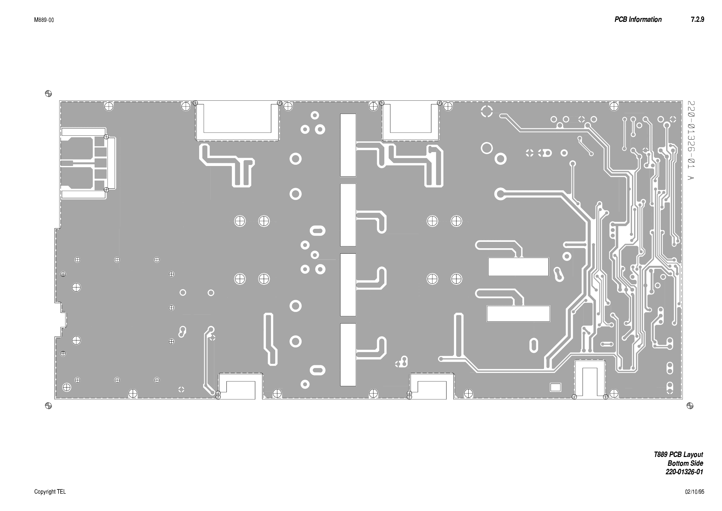
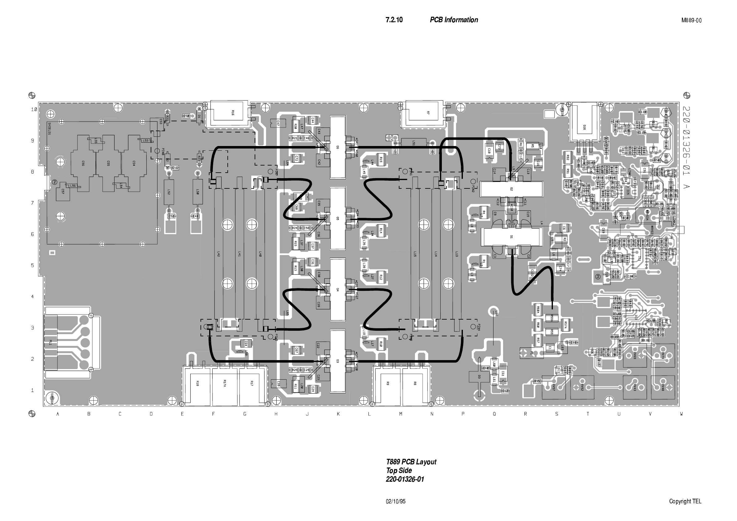
L46
C97 C98
L19
L29
L96
C59
L22 L16
L32 L26
L1
L49 L43L12
L39 L33
C45 C38
C15
C32
C25