CHIPSEA TECHNOLOGIES CSM84F12 WIFI Module CSM84F12 User Manual
CHIPSEA TECHNOLOGIES (SHENZHEN) CORP. WIFI Module CSM84F12 Users Manual
Contents
- 1. Users Manual
- 2. User manual_CSM84F12
- 3. User manual_user RF statement
Users Manual
1 / 13
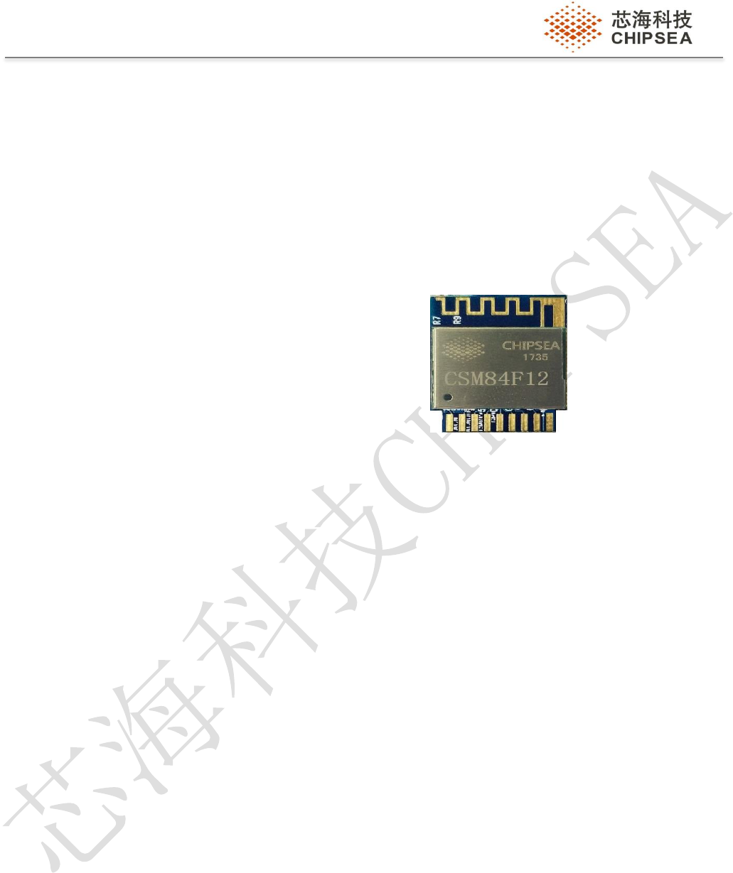
CSM84F12 IOT Module
Data Sheet
V1.0
June.2018
聚点滴之芯.成浩瀚之海
2 / 13
Table of Contents
1. Introduction ............................................................................................................................. 3
1.1 General Description ..........................................................................................................................3
1.2 Hardware Description ......................................................................................................................3
2. System Block Diagram .............................................................................................................. 4
3. CSM84F12 Pin-out .................................................................................................................... 5
3.1 Pin-out view ......................................................................................................................................5
3.2 CSM84F12 Pin Assignment and Descriptions .................................................................................5
4. Electrical Specifications .......................................................................................................... 6
4.1 Absolute Maximum Ratings .............................................................................................................6
4.2 Environmental Ratings .....................................................................................................................7
4.2.1 Storage Condition .................................................................................................................................7
4.3 Thermal Characteristics ...................................................................................................................7
4.4 PMU Under Voltage Lock-out (UVLO) Characteristics ....................................................................8
4.5 Electrostatic Discharge Specifications ............................................................................................8
4.6 Recommended Operating Conditions and DC Characteristics .......................................................8
5. Electrical Specifications ...................................................................................................... 10
5.1 Transmitter Characteristics for 2.4GHz Operation ...................................................................... 10
5.2 Receiver Characteristics for 2.4GHz Operation ............................................................................ 11
6. System Power Consumption ............................................................................................... 11
7. Soldering Recommendations ................................................................................................. 11
Appendix A: HW Reference Design ...................................................................................................... 13
聚点滴之芯.成浩瀚之海
3 / 13
1. Introduction
1.1 General Description
The CSM84F12 module is an intelligent Internet of Everything platform enables customers to add Wi-Fi to a
wide variety of products with minimal development effort and cost.
1.2 Hardware Description
CST84F11+CSE7761
Size: 18 x 18 x 3.5mm±0.1mm
Operating voltage: 3.3 V ± 5%
16Mbit flash
192KB SRAM
Support FlyOS FlyLink
RF interface
Internal PIFA antenna
Operating temperature range:
Commercial: -20°C ~ +85°C
Power consumption
Transmit: 290 mA @18dBm
Receive: TBD
Standby mode (Sleep): TBD
Deep sleep: TBD
Package:
Golden Finger: 18 PADs
Host interface: GPIO X 12,UART, SPI,UART, PWM
WiFi mode support:
Station
Soft AP
Station + Soft AP
Active Power Accuracy: ±0.1% error of Reading over 8000:1 Dynamic Range.
Voltage and Current Active Power Accuracy: ±0.1% error of Reading over 1000:1 Dynamic Range.
聚点滴之芯.成浩瀚之海
4 / 13
Active value Accuracy: ±0.1% error of Reading over 1000:1 Dynamic Range.
On-chip 1.25 V Reference (5ppm/°C typ, <20 ppm/°C max).
Leakage Function: Leakage current 30mA, < 30ms reaction time.
System Calibrations Function: ±100% Calib Range
Phase Compensation Funciton: ±2.56°Compensate Range, 0.02° minimum Compensating value.
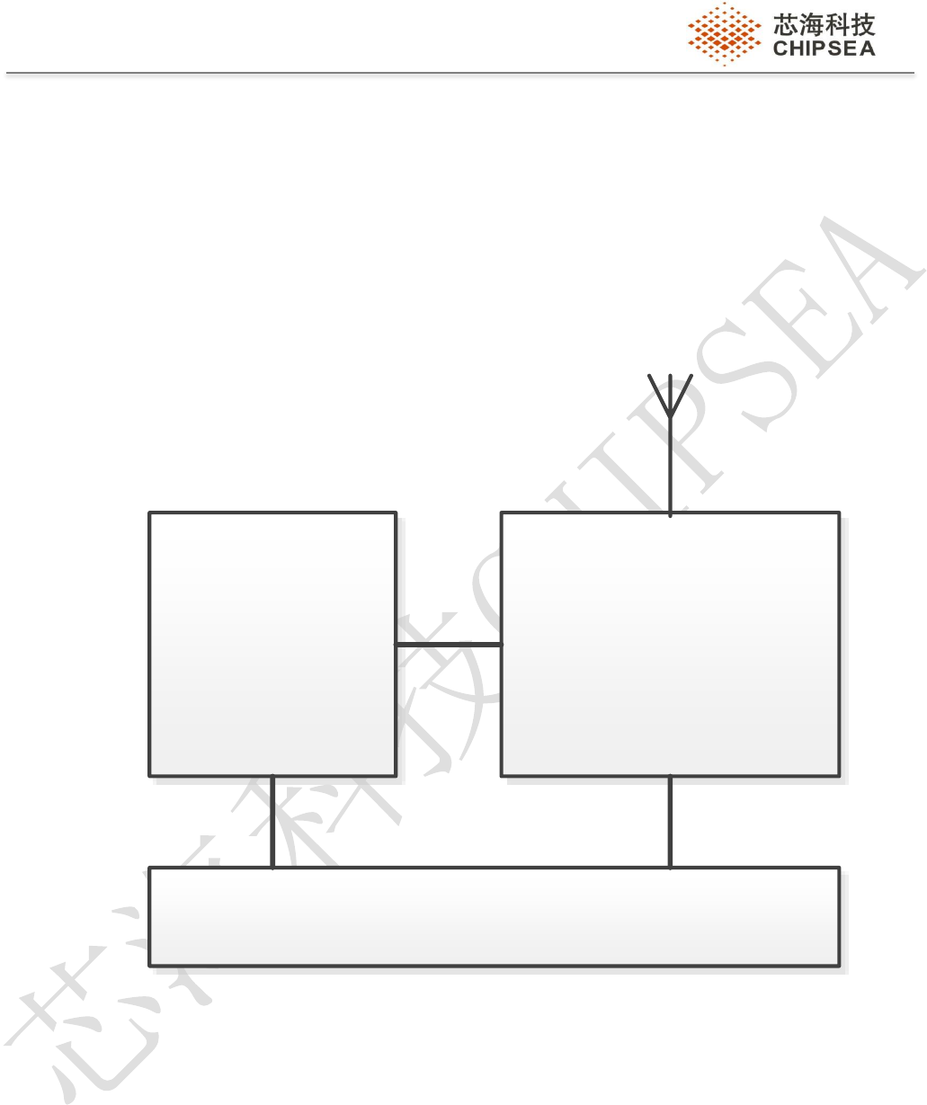
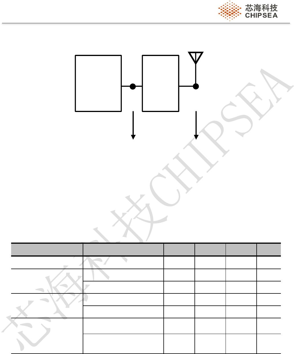
2. System Block Diagram
CST84F11
ANT
2.4G
Power 3.3V
CSE7761
聚点滴之芯.成浩瀚之海
5 / 13
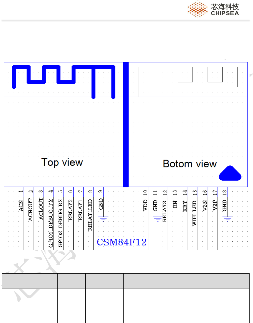
3. CSM84F12 Pin-out
3.1 Pin-out view
3.2 CSM84F12 Pin Assignment and Descriptions
Symbol
Type
Pin
Description
ACN
I/O
1
IIN1+ Differential analog input pins for the current
channel
ACNOUT
I/O
2
IIN1- Differential analog input pins for the current
channel
聚点滴之芯.成浩瀚之海
6 / 13
Symbol
Type
Pin
Description
ACLOUT
I/O
3
VIN- Differential analog input pins for the voltage
channel
GPIO1_DEBUG_TX
I/O
4
TXD
GPIO3_DEBUG_RX
I/O
5
RXD
RELAY2
I/O
6
GPIO controller for relay1
RELAY1
I/O
7
GPIO controller for relay2
RELAY_LED
I/O
8
LED for RELAY
VDD
-
10
3.3V supply for whole module
RELAY3
I/O
12
GPIO controller for relay3
EN
I/O
13
Enable chip.
1: enable chip;
0: Shutdown Chip
KEY
I/O
14
key
WIFI_LED
I/O
15
LED to indicator statues of WIFI
V2N
I/O
16
IIN2+ Differential analog input pins for the current
channel
V2P
I/O
17
IIN2- Differential analog input pins for the current
channel
GND
-
9
Ground
-
11
-
18
4. Electrical Specifications
4.1 Absolute Maximum Ratings
The absolute maximum ratings in Table 4-1 indicate levels where permanent damage to the device can
occur, even if these limits are exceeded for only a brief duration. Functional operation is not guaranteed under
these conditions. Operation at absolute maximum conditions for extended periods can adversely affect long-
term reliability of the device.
Table 4-1: Absolute Maximum Ratings
聚点滴之芯.成浩瀚之海
7 / 13
4.2 Environmental Ratings
The environmental ratings are shown in Table 4-2
Table 4-2 Environmental Ratings
Characteristic
Conditions/Comments
Value
Units
Ambient Temperature (TA)
Functional operation
-20 to +85
°C
4.2.1 Storage Condition
The calculated shelf life in sealed bag is 12 months if stored between 0°C and 40°C at less than 90%
relative humidity (RH). After the bag is opened, devices that are subjected to solder reflow or other high
temperature processes must be handled in the following manner:
a) Mounted within 168-hours of factory conditions < 30 °C /60%RH
b) Storage humidity needs to maintained at <10% RH
c) Baking is necessary if customer exposes the component to air over 168 hours, Baking condition:
125°C / 8hrs
4.3 Thermal Characteristics
Table 4-3: the thermal characteristics of the CSM84F12.
Thermal characteristics without external heat sink in still air condition
Symbol
Description
Typ.
Unit
TJ
Maximum Junction Temperature (Plastic Package)
125
°C
θJA
Thermal Resistance θJA (°C /W) for JEDEC 4L system PCB
57.7
°C/W
θJC
Thermal Resistance θJC (°C /W) for JEDEC 4L system PCB
TBD
°C/W
ΨJt
Thermal Characterization parameter ΨJt (°C /W) for JEDEC
4L system PCB
7.9
°C/W
Maximum Lead Temperature (Soldering 10s)
260
°C
Notes: * Thermal characteristics without external heat sink in still air condition
Symbol (domain)
Description
Max Rating
Unit
EFUSE_VDD
VDD input for EFUSE burn-in.
Pull low when read mode
-0.3 to 2.75
V
VBAT
VDD input
-0.3 to 3.6
V
ACLOUT , ACNOUT , V2P, V2N
-1 to 6
V
聚点滴之芯.成浩瀚之海
8 / 13
4.4 PMU Under Voltage Lock-out (UVLO) Characteristics
Table 4-4 PMU UVLO characteristics
Symbol (domain)
Description
Min.
Typ.
Max.
Unit
Under Voltage Lock-Out (UVLO)
Under voltage rising
threshold of VBAT
VDD33: ball VBAT
2.95
V
Under voltage falling
threshold of VBAT
VDD33: ball VBAT
2.85
V
4.5 Electrostatic Discharge Specifications
This is an ESD sensitive product! Observe precaution and handle with care. Extreme caution must be
exercised to prevent electrostatic discharge (ESD) damage. Proper use of wrist and heel grounding straps to
discharge static electricity is required when handling these devices.
Table 4-5: ESD Specifications
Pin Type
Test Condition
ESD Rating
Unit
Human Body Mode
(HBM)
refers to MIL-STD-883G Method
3015.7
Pass ±2.5
KV
Machine Mode (MM)
refers to JEDEC EIA/JESD22-A115
Pass ±250
V
4.6 Recommended Operating Conditions and DC Characteristics
Table 4-6: Recommended Operating Conditions and DC Characteristics
Domain (Symbol)
Description
Min.
Typ.
Max.
Unit
VDD16_DCDC_OUT
LDO/Buck converter 1.6V output
1.7
V
EFUSE_VDD
VDD input for EFUSE burn-in.
Pull low when read mode
2.25
2.5
2.75
V
DVDD12
VDD output for internal digital
circuit
1.3
V
VDD12_RTC_OUT
VDD output for internal RTC
circuit
1.3
V
VBAT
3.3V supply
3.14
3.3
3.46
V
(VIL)
Input Low voltage when
-0.3
0.8
V
聚点滴之芯.成浩瀚之海
9 / 13
VBAT=3.3V
(VIH)
Input High voltage when
VBAT=3.3V
2
3.6
V
(VT+)
Schmitt trigger low to high
threshold voltage when
VBAT=3.3V
1.6
1.74
1.89
V
(VT-)
Schmitt trigger high to low
threshold voltage when
VBAT=3.3V
1.27
1.4
1.56
V
(VOL)
Output low voltage when
VBAT=3.3V
0.4
V
(VOH)
Output high voltage when
VBAT=3.3V
2.4
V
(RPD)
Input weakly pull-down resistance
when VBAT=3.3V.
All GPIO pins have internal
weakly pull- down option except
that GPIO_5 has internal weakly
pull-up option
35
51
84
KΩ
(IOL)
Low level output current @
VOL(max), 8mA setting
11.9
17.7
23.4
mA
Low level output current @
VOL(max), 12mA setting
15.8
23.5
31.1
mA
(IOH)
High level output current @
VOH(min), 8mA setting
17.2
34.1
58.8
mA
High level output current @
VOH(min), 12mA setting
23.9
47.2
81.5
mA
聚点滴之芯.成浩瀚之海
10 / 13
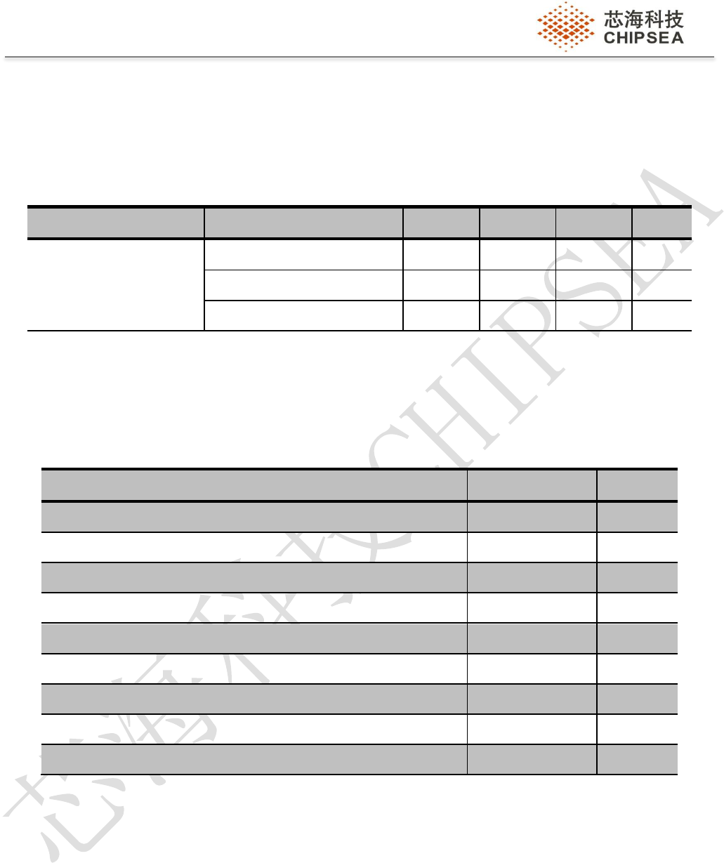
5. Electrical Specifications
RF_IO
Antenna
Matching
RF Port Antenna Port
Figure 5-1: RF Front-End Reference Topology for RF Performance
Note: All specifications are measured at the Antenna Port unless otherwise specified.
5.1 Transmitter Characteristics for 2.4GHz Operation
Table 5-1 summarizes the transmitter characteristics for the CSM84F12.
Table 5-1 transmitter characteristics
Parameter
Condition/Notes
Min.
Typ.
Max.
Unit
Frequency Range
2412
-
2484
MHz
Rx Sensitivity
(CCK)
CCK, 1 Mbps
-94.0
dBm
CCK, 11 Mbps
-87.0
dBm
Rx Sensitivity
(OFDM)
OFDM, 6 Mbps
-91.0
dBm
OFDM, 54 Mbps
-72.0
dBm
Rx Sensitivity (HT20)
Greenfield 800nS GI
Non-STBC
HT20, MCS0
-91.0
dBm
HT20, MCS7
-68.0
dBm
聚点滴之芯.成浩瀚之海
11 / 13
5.2 Receiver Characteristics for 2.4GHz Operation
Table 5-2 summarizes the receiver characteristics for the CSM84F12. Notice that transmitter and
especially receiver characteristics must be test under test guider.
Table 5-2 receiver characteristics
Parameter
Condition/Notes
Min.
Typ.
Max.
Unit
TX Output Power
CCK, 1-11 Mbps
17.5
dBm
OFDM, 54 Mbps
14.0
dBm
HT20, MCS7
14.0
dBm
6. System Power Consumption
Note: All results are measured at the condition that VBAT are 3.3V.
Table 6-1: Power Consumption
WLAN Operational Modes
Typ.
Unit
Rx, CCK, 1 Mbps(Continuous)
91
mA
Rx, OFDM, 54 Mbps(Continuous)
101
mA
Rx, HT20, MCS7(Continuous)
103
mA
Tx, CCK, 1 Mbps, 19dBm(Continuous)
292
mA
Tx, OFDM, 54 Mbps, 16dBm(Continuous)
237
mA
Tx, HT20, MCS7, 15dBm(Continuous)
239
mA
Normal work(Avg)
30
mA
Tx&Rx (Avg for DCDC mode, normal usage)
80
mA
Tx&Rx (Avg for LDO mode, normal usage)
100
mA
7. Soldering Recommendations
The CSM84F12 module can be SMT on the board following the temperature curve graph:
聚点滴之芯.成浩瀚之海
12 / 13
Figure 7-1: CSM84F12 temperature curve graph
Table 7-1: Solder Profile Section
Profile Section
Profile Feature
Pb-free Package
1
Preheat
- Temperature min (Tsmin)
- Temperature max.(Tsmax)
- Time (min. to max.)
150°C
200°C
60 ~ 180 seconds
2
Tsmax ro TL
- Ramp-up rate
3°C /second max.
3
Time maintained above:
- Temperature (TL)
- Time
217°C
60 ~ 150 seconds
Average ramp-up rate (TL to Tp)
3°C /second max.
4
Peak Temperature (Tp)
250±5°C
Time within 5℃ of actual peak temperature
(tp)
20 ~ 40 seconds
5
Ramp-down rate
6°C /second max.
Time 25°C to peak temperature
8 minutes max.
聚点滴之芯.成浩瀚之海
13 / 13
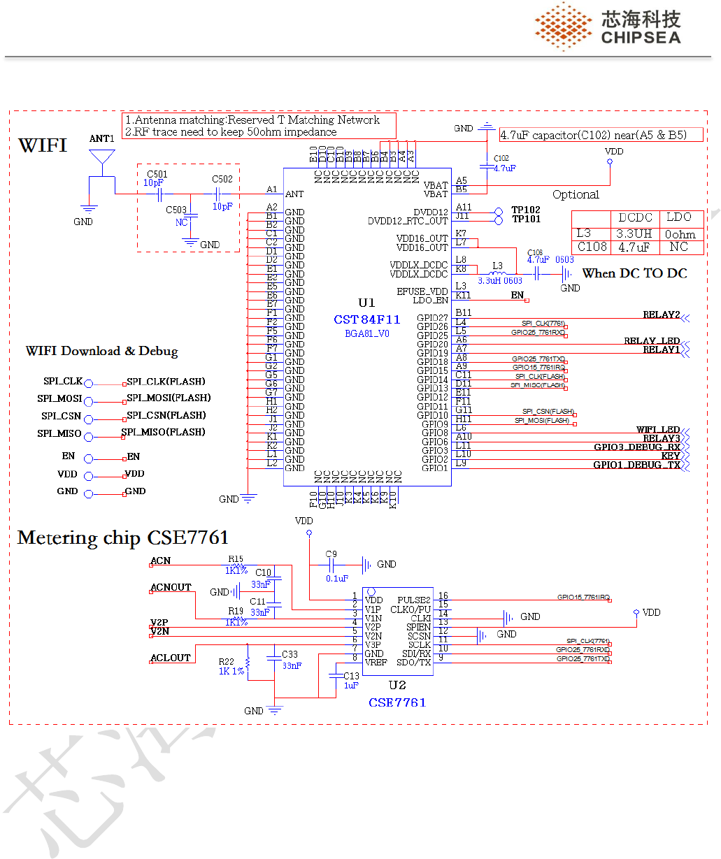
Appendix A: HW Reference Design