COMMAX CMX-ZG03 Zigbee Module User Manual
COMMAX Co., Ltd. Zigbee Module
UserManual.wiki
>
COMMAX
>
CMX-ZG03 User Manual
>
User Manual
Contents
1.
User Manual
2.
User Manual 700MHost product
3.
User Manual 1020MHost product
User Manual
Navigation menu
Upload a User Manual
Namespaces
Wiki Guide
HTML
PDF
Info
Views
User Manual
Discussion / Help
Navigation

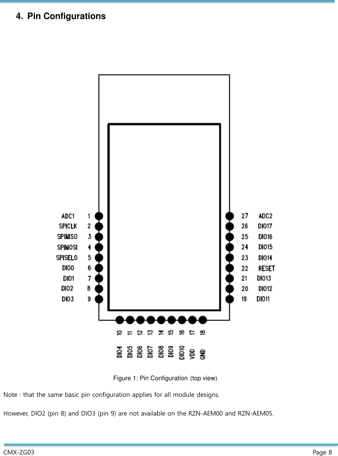
![CMX-ZG03 Page 9 4.1. Pin Assignment SymbolPinType[1] DescriptionDO0/SPICLK/PWM2[2] 2ODO0 — DO0SPICLK — SPI-bus master clock outputPWM2 — PWM2 outputDO1/SPIMISO/PWM3[3] 3I/ODO1 — DO1SPIMISO — SPI-bus Master In, Slave Out inputPWM3 — PWM3 outputDIO18/SPIMOSI4I/ODIO18 — DIO18SPIMOSI — SPI-bus Master Out Slave In outputDIO19/SPISEL05I/ODIO19 — DIO19SPISEL0 — SPI-bus Master Select Output 0DIO0/ADO/SPISEL1/ADC36I/ODIO0 — DIO0ADO — antenna diversity odd outputSPISEL1 — SPI-bus master select output 1ADC3 — ADC input: ADC3DIO1/ADE/SPISEL2/ADC4/PC07I/ODIO1 — DIO1ADE — antenna diversity even outputSPISEL2 — SPI-bus master select output 2ADC4 — ADC input: ADC4PC0 — pulse counter 0 inputDIO2/RFRX/TIM0CK_GT/ADC5[4] 8I/ODIO2 — DIO2RFRX — radio receives control outputTIM0CK_GT — timer0 clock/gate inputADC5 — ADC input: ADC5DIO3/RFTX/TIM0CAP/ADC6[4] 9I/ODIO3 — DIO3RFTX — radio transmit control outputTIM0CAP — timer0 capture inputADC6 — ADC input: ADC6DIO4/CTS0/JTAG_TCK/TIM0OUT/PC010I/ODIO4 — DIO4CTS0 — UART 0 clear to send inputJTAG_TCK — JTAG CLK inputTIM0OUT — timer0 PWM outputPC0 — pulse counter 0 inputDIO5/RTS0/JTAG_TMS/PWM1/PC111I/ODIO5 — DIO5RTS0 — UART 0 request to send outputJTAG_TMS — JTAG mode select inputPWM1 — PWM1 outputPC1 — pulse counter 1 inputDIO6/TXD0/JTAG_TDO/PWM212I/ODIO6 — DIO6TXD0 — UART 0 transmit data outputJTAG_TDO — JTAG data outputPWM2 — PWM2 data output](https://usermanual.wiki/COMMAX/CMX-ZG03.User-Manual/User-Guide-3394450-Page-9.png)
![CMX-ZG03 Page 10 SymbolPinType[1] DescriptionDIO7/RXD0/JTAG_TDI/PWM313I/ODIO7 — DIO7RXD0 — UART 0 receive data inputJTAG_TDI — JTAG data inputPWM3 — PWM 3 data outputDIO8/TIM0CK_GT/PC1/PWM414I/ODIO8 — DIO8TIM0CK_GT — timer0 clock/gate inputPC1 — pulse counter1 inputPWM4 — PWM 4 outputDIO9/TIM0CAP/32KXTALIN/RXD1/32KIN15I/ODIO9 — DIO9TIM0CAP — Timer0 Capture input32KXTALIN — 32 kHz External Crystal inputRXD1 — UART1 Receive Data input32KIN — 32 kHz External clock inputDIO10/TIM0OUT/32KXTALOUT16I/ODIO10 — DIO10TIM0OUT — Timer0 PWM Output32KXTALOUT — 32 kHz External Crystal outputVDD 17PVDD — supply voltage VSS 18GNDgroundDIO11/PWM1/TXD119I/ODIO11 — DIO11PWM1 — PWM1 outputTXD1 — UART1 Transmit Data outputDIO12[5] 20I/ODIO12 — DIO12PWM2 — PWM2 outputCTS0 — UART0 clear to send inputJTAG_TCK — JTAG CLK inputADO — antenna diversity odd outputSPISMOSI — SPI-bus slave Master Out, Slave In inputDIO13[6] 21I/ODIO13 — DIO13PWM3 — PWM3 outputRTS0 — UART0 request to send outputJTAG_TMS — JTAG mode select inputADE — antenna diversity even outputSPISMISO — SPI-bus slave master in slave out outputRESET_N22IRESET_N — reset inputDIO14[7] 23I/ODIO14 — DIO14SIF_CLK — serial interface clockTXD0 — UART 0 transmit data outputTXD1 — UART 1 transmit data outputJTAG_TDO — JTAG data outputSPISEL1 — SPI-bus master select output 1SPISSEL — SPI-bus slave select input](https://usermanual.wiki/COMMAX/CMX-ZG03.User-Manual/User-Guide-3394450-Page-10.png)
![CMX-ZG03 Page 11 SymbolPinType[1] DescriptionDIO15[8] 24I/ODIO15 — DIO15SIF_D — serial interface dataRXD0 — UART 0 receive data inputRXD1 — UART 1 receive data inputJTAG_TDI — JTAG data inputSPISEL2 — SPI-bus master select output 2SPISCLK — SPI-bus slave clock inputDIO16/SPISMOSI/SIF_CLK/COMP1P25I/ODIO16 — DIO16COMP1P — comparator positive inputSIF_CLK — Serial Interface clockSPISMOSI — SPI-bus Slave Master Out Slave In inputDIO17/SPISMISO/SIF_D/COMP1M26I/ODIO17 — DIO17COMP1M — COMP1M; comparator negative inputSIF_D — Serial Interface DataSPISMISO — SPI-bus Slave Master In Slave Out outputPWM4 — PWM 4 outputVREF/ADC227PVREF — analog peripheral reference voltageIADC2 — ADC input 2[1] P = power supply; G = ground; I = input, O = output; I/O = input/output. [2] JTAG programming mode: must be left floating high during reset to avoid entering JTAG programming mode. [3] UART programming mode: leave pin floating high during reset to avoid entering UART programming mode or hold it low to program [4] Not available on the JN5169-001-M06-2 since they are used to control the front-end module. [5] Multi-function: DIO12/PWM2/CTS0/JTAG_TCK/ADO/SPISMOSI. [6] Multi-function: DIO13/PWM3/RTS0/JTAG_TMS/ADE/SPISMISO. [7] Multi-function: DIO14/SIF_CLK/TXD0/TXD1/JTAG_TDO/SPISEL1/SPISSEL. [8] Multi-function: DIO15/SIF_D/RXD0/RXD1/JTAG_TDI/SPISEL2/SPISCLK.](https://usermanual.wiki/COMMAX/CMX-ZG03.User-Manual/User-Guide-3394450-Page-11.png)