Contents
User Manual

CMX-ZG03
Datasheet
(VER.0.0)
CMX-ZG03 Page 2
Data Sheet : CMX-ZG03
ZigBee 3.0 , ZigBee PRO and IEEE802.15.4 Module
Overview
CMX-ZG03은 using the
IEEE802.15.4 standard in the 2.4 GHz - 2.5 GHz ISM frequency band,
including ZigBee 3.0 and ZigBee PRO stack with Home Automation, Light Link and Smart
Energy profiles.
The modules integrate all of the RF components required, removing the need to
perform
expensive RF design and test. Products can be designed by simply connecting sensors
and switches to the module IO pins. The modules use JN51xx single chip IEEE802.15.4
wireless
microcontroller, allowing designers to make use of the extensive chip
development support
material. Hence, this range of modules allows designers to bring
wireless applications to market
in the minimum time with significantly reduced
development effort and cost.
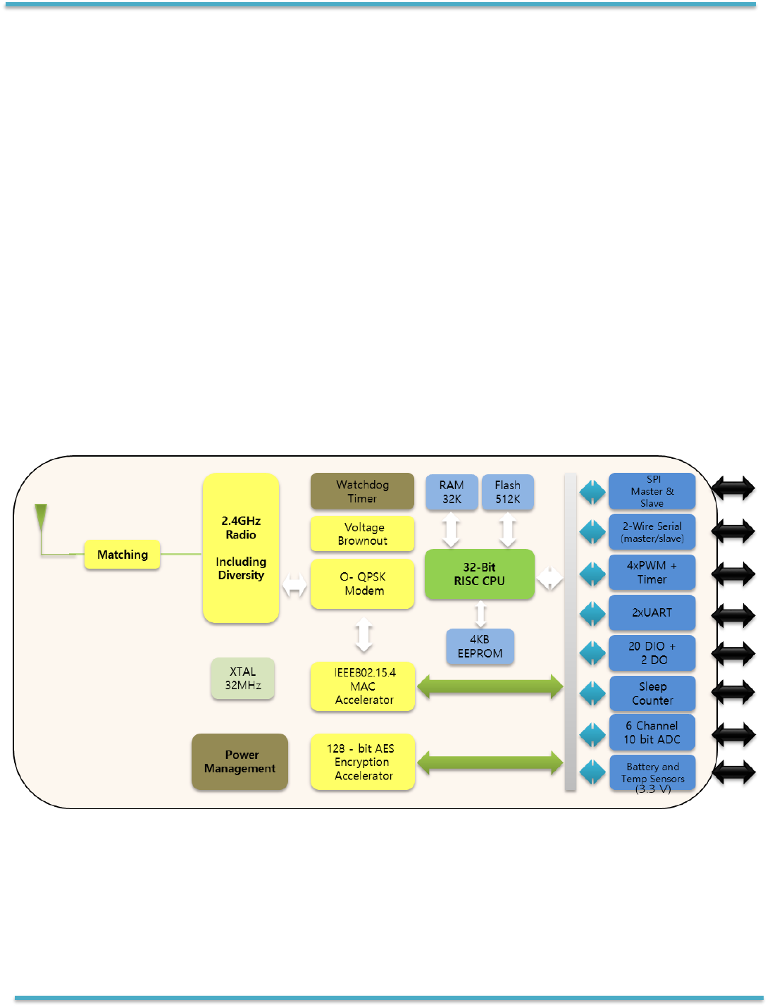
Module Block Diagram

CMX-ZG03 Page 3
Benefits
•Microminiature module solutions
•Ready to use in products
•Minimises product development time
•No RF test required for systems
Applications
• Robust and secure low-power wireless applications
• ZigBee Smart Energy networks
• ZigBee Home Automation networks
• Toys and gaming peripherals
• Energy harvesting - for example, self-powered light switch
Features: Module
•2.4GHz IEEE 802.15.4, , ZigBee 3.0 and ZigBee PRO stack with Home Automation,
ZigBee Light Link, ZigBee Smart Energy
•CMX-ZG03
CMX-ZG03 : integral antenna 16x28mm
o8.5dBm/10dBm TX Power
oReceiver sensitivity -96dBm
oTX current 27.2 mA at 10 dBm
oTX current 23.6 mA at 8.5 dBm
oRX current 17.8 mA at maximum input level 10 dBm
oRX current 16.2 mA at maximum input level 0 dBm
o2.0-3.6V operation
Features: Microcontroller
•32-bit RISC CPU; 1 MHz to 32 MHz clock speed
• Variable instruction width for high coding efficiency
• Multi-stage instruction pipeline
• 512 kB Flash
• 32 kB RAM
• 4 kB EEPROM
• Data EEPROM with guaranteed 100 k write operations
• 2-wire I2C-bus compatible serial interface; can operate as either master or slave
•5 PWM (4 timers, 1 timer/counter)
• 2 low-power sleep counters
• 2 UARTs
•SPI-bus Master and Slave port, 3 selects
• Supply voltage monitor with 8 programmable thresholds
• 6-input 10-bit ADC, comparator
• Battery and temperature sensors
• Watchdog and Supply Voltage Monitor (SVM)
• Up to 20 Digital IO (DIO) pins
Industrial temp (-40°C to +85°C)
Lead-free and RoHS compliant

CMX-ZG03 Page 4
Contents
1. Introduction ……………………………………………………………………………………5
1.1. Variants…………………………………………………………………………………………………….. 5
2. Specifications………………………………………………………………………………….6
3. Product Development………………………………………………………………………...7
3.1. JN5XXX Single Chip Wireless Microcontroller……………..……………………….…………….…….7
4. Pin Configurations………………………………………………………….………….…..…8
4.1. Pin Assignment……………………………………………………………………………………..….…. 9
4.2. Pin Descriptions………………………………..……………………………………………………...… 12
4.2.1 Power Supplies…………………………………..………………………………………………… 12
5. Electrical Characteristics………………………………………………………………..….12
5.1. Maximum Ratings……………………………………………………..…………………………………. 12
5.2. Operating Conditions……………………………………………………..……………………………… 12
6.Module External Circuit for Programming….....…..………………………………..….13
Appendix A Additional Information……………….….…………………………………..….14
A.1. Outline Drawing : CMX-ZG03....…………………………………………………………….……………14
A.2. Module PCB Footprint………………………………………………………………………………..……15

CMX-ZG03 Page 5
1. Introduction
CMX-ZG03 is a range of ultra-low power, high performance surface
mount modules targeted at
IEEE 802.15.4, ZigBee 3.0 and ZigBee Home Automation,
Light Link and Smart Energy
networking applications, enabling users to realize products
with minimum time to market and at
the lowest cost. They remove the need for expensive
and lengthy development of custom RF
board designs and test suites. The modules use JN51xx wireless microcontroller to provide a
comprehensive solution with large
memory, high CPU and radio performance and all RF
components included. All that is
required to develop and manufacture wireless control or
sensing products is to connect a
power supply and peripherals such as switches, actuators
and sensors, considerably
simplifying product development.
module variants are available.
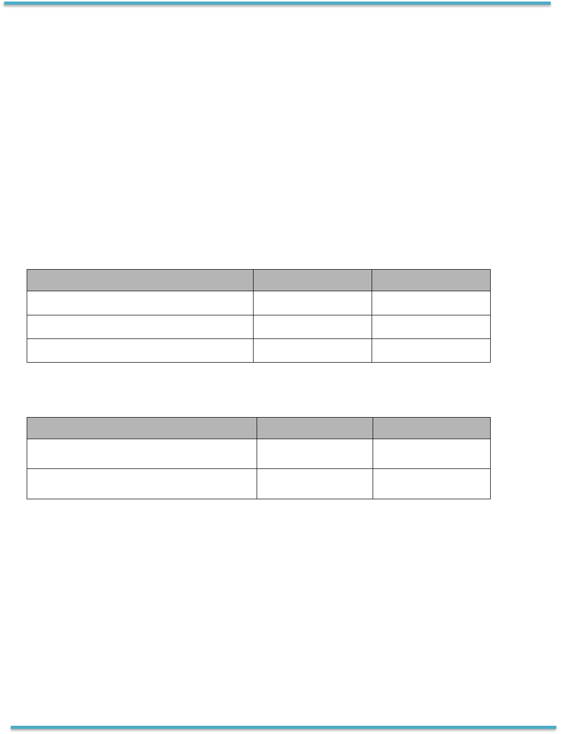
1.1. Variants
Variant
Description
CMX-ZG03
integrated antenna

CMX-ZG03 Page 6
2. Specifications
VDD=3.0V @ +25°C
Typical DC Characteristics
Notes
CMX-ZG03
Deep sleep current
70nA
Sleep current
0.73uA
In sleep mode; with I/O and RC oscillator
timer wake-up;
Radio transmit
current
25mA
10dBm @2.8V
Radio receive
current
17.8mA
Maximu input level at 10dBm
Centre frequency
accuracy
+/-25ppm
Additional +/-15ppm allowance for
temperature and ageing
Typical RF Characteristics
Notes
Receive sensitivity
-96dBm
Nominal for 1% PER, as per 802.15.4
section 6.5.3.3 (Note 1)
Transmit power
10dBm
22dBm
9.5 dBm
Nominal
Maximum input
signal
10dBm
For 1% PER, measured as sensitivity
RSSI range
-95 to
-10dBm
RF Port impedance
–uFL connector
50 ohm
2.4 - 2.5GHz
Rx Spurious
Emissions
-70dBm
Measured conducted into 50ohms
Tx Spurious
Emissions
-36dBm
Measured conducted into 50ohms
VSWR (max)
2:1
2.4 - 2.5GHz
Peripherals
Notes
Master SPI port
3 selects
3 selects
3 selects
250kHz - 16MHz
Slave SPI port
1
250kHz - 4MHz
Two UARTs
2
16550 compatible
Two-wire serial I/F
(compatible with
SMbus & I2C)
1
Up to 400kHz
PWM
4 x timer, 1 x timer/counter
16MHz clock
Two programmable
Sleep Timers
2
32kHz clock
Digital IO lines
( multiplexed with
UARTs, timers and
SPI selects )
20
DIO2 & DIO3 not available on RZN-AEM00
and RZN-AEM01 modules
Analogue-to-Digital
converter
6
10-bit, up to 100ks/s

CMX-ZG03 Page 7
Programmable
analogue
comparators
1
Ultra low power mode for sleep
Internal
temperature sensor
and battery monitor
1
3. Product Development
A range of evaluation/developer kits is also available, allowing products to be quickly bread
boarded. Efficient development of software applications is enabled by the provision of a complete,
unlimited, software developer kit. Together with the available libraries for the IEEE802.15.4 MAC
and the ZigBee PRO network stacks, this package provides everything required to develop
application code and to trial it with hardware representative of the final module.
The modules can be user programmed both in development. Access to the on-chip peripherals,
MAC and network stack software is provided through specific APIs.
3.1. JN51xx Single Chip Wireless Microcontroller
CMX-ZG03 is constructed around the JN51XX single chip wireless microcontroller, which includes
the radio system, a 32-bit RISC CPU, Flash, RAM & EEPROM memory and a range of analogue
and digital peripherals.
CMX-ZG03 Page 8
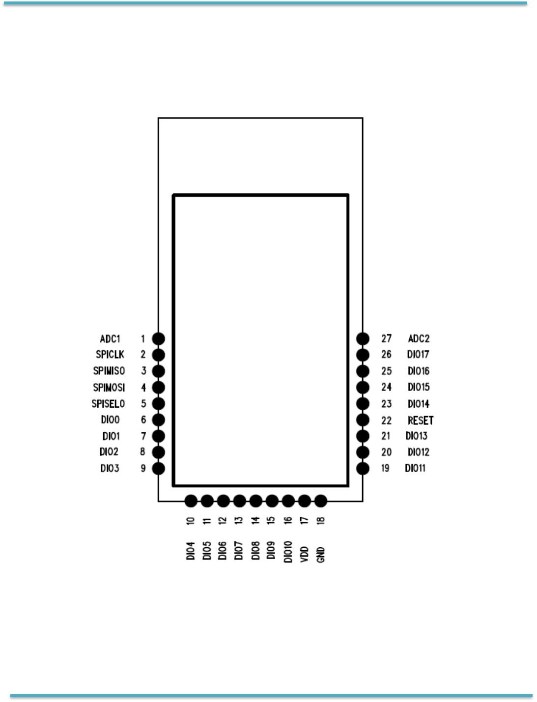
4. Pin Configurations
Figure 1: Pin Configuration (top view)
Note : that the same basic pin configuration applies for all module designs.
However, DIO2 (pin 8) and DIO3 (pin 9) are not available on the RZN-AEM00 and RZN-AEM05.

CMX-ZG03 Page 9
4.1. Pin Assignment
Symbol
Pin
Type[1]
Description
DO0/SPICLK/PWM2[2]
2
O
DO0 — DO0
SPICLK — SPI-bus master clock output
PWM2 — PWM2 output
DO1/SPIMISO/PWM3[3]
3
I/O
DO1 — DO1
SPIMISO — SPI-bus Master In, Slave Out input
PWM3 — PWM3 output
DIO18/SPIMOSI
4
I/O
DIO18 — DIO18
SPIMOSI — SPI-bus Master Out Slave In output
DIO19/SPISEL0
5
I/O
DIO19 — DIO19
SPISEL0 — SPI-bus Master Select Output 0
DIO0/ADO/SPISEL1/ADC3
6
I/O
DIO0 — DIO0
ADO — antenna diversity odd output
SPISEL1 — SPI-bus master select output 1
ADC3 — ADC input: ADC3
DIO1/ADE/SPISEL2/ADC4/PC0
7
I/O
DIO1 — DIO1
ADE — antenna diversity even output
SPISEL2 — SPI-bus master select output 2
ADC4 — ADC input: ADC4
PC0 — pulse counter 0 input
DIO2/RFRX/TIM0CK_GT/ADC5[4]
8
I/O
DIO2 — DIO2
RFRX — radio receives control output
TIM0CK_GT — timer0 clock/gate input
ADC5 — ADC input: ADC5
DIO3/RFTX/TIM0CAP/ADC6[4]
9
I/O
DIO3 — DIO3
RFTX — radio transmit control output
TIM0CAP — timer0 capture input
ADC6 — ADC input: ADC6
DIO4/CTS0/JTAG_TCK/TIM0OUT/PC0
10
I/O
DIO4 — DIO4
CTS0 — UART 0 clear to send input
JTAG_TCK — JTAG CLK input
TIM0OUT — timer0 PWM output
PC0 — pulse counter 0 input
DIO5/RTS0/JTAG_TMS/PWM1/PC1
11
I/O
DIO5 — DIO5
RTS0 — UART 0 request to send output
JTAG_TMS — JTAG mode select input
PWM1 — PWM1 output
PC1 — pulse counter 1 input
DIO6/TXD0/JTAG_TDO/PWM2
12
I/O
DIO6 — DIO6
TXD0 — UART 0 transmit data output
JTAG_TDO — JTAG data output
PWM2 — PWM2 data output

CMX-ZG03 Page 10
Symbol
Pin
Type[1]
Description
DIO7/RXD0/JTAG_TDI/PWM3
13
I/O
DIO7 — DIO7
RXD0 — UART 0 receive data input
JTAG_TDI — JTAG data input
PWM3 — PWM 3 data output
DIO8/TIM0CK_GT/PC1/PWM4
14
I/O
DIO8 — DIO8
TIM0CK_GT — timer0 clock/gate input
PC1 — pulse counter1 input
PWM4 — PWM 4 output
DIO9/TIM0CAP/32KXTALIN/RXD1/32KIN
15
I/O
DIO9 — DIO9
TIM0CAP — Timer0 Capture input
32KXTALIN — 32 kHz External Crystal input
RXD1 — UART1 Receive Data input
32KIN — 32 kHz External clock input
DIO10/TIM0OUT/32KXTALOUT
16
I/O
DIO10 — DIO10
TIM0OUT — Timer0 PWM Output
32KXTALOUT — 32 kHz External Crystal output
VDD
17
P
VDD — supply voltage
VSS
18
GND
ground
DIO11/PWM1/TXD1
19
I/O
DIO11 — DIO11
PWM1 — PWM1 output
TXD1 — UART1 Transmit Data output
DIO12[5]
20
I/O
DIO12 — DIO12
PWM2 — PWM2 output
CTS0 — UART0 clear to send input
JTAG_TCK — JTAG CLK input
ADO — antenna diversity odd output
SPISMOSI — SPI-bus slave Master Out, Slave In input
DIO13[6]
21
I/O
DIO13 — DIO13
PWM3 — PWM3 output
RTS0 — UART0 request to send output
JTAG_TMS — JTAG mode select input
ADE — antenna diversity even output
SPISMISO — SPI-bus slave master in slave out output
RESET_N
22
I
RESET_N — reset input
DIO14[7]
23
I/O
DIO14 — DIO14
SIF_CLK — serial interface clock
TXD0 — UART 0 transmit data output
TXD1 — UART 1 transmit data output
JTAG_TDO — JTAG data output
SPISEL1 — SPI-bus master select output 1
SPISSEL — SPI-bus slave select input

CMX-ZG03 Page 11
Symbol
Pin
Type[1]
Description
DIO15[8]
24
I/O
DIO15 — DIO15
SIF_D — serial interface data
RXD0 — UART 0 receive data input
RXD1 — UART 1 receive data input
JTAG_TDI — JTAG data input
SPISEL2 — SPI-bus master select output 2
SPISCLK — SPI-bus slave clock input
DIO16/SPISMOSI/SIF_CLK/COMP1P
25
I/O
DIO16 — DIO16
COMP1P — comparator positive input
SIF_CLK — Serial Interface clock
SPISMOSI — SPI-bus Slave Master Out Slave In input
DIO17/SPISMISO/SIF_D/COMP1M
26
I/O
DIO17 — DIO17
COMP1M — COMP1M; comparator negative input
SIF_D — Serial Interface Data
SPISMISO — SPI-bus Slave Master In Slave Out output
PWM4 — PWM 4 output
VREF/ADC2
27
P
VREF — analog peripheral reference voltage
I
ADC2 — ADC input 2
[1] P = power supply; G = ground; I = input, O = output; I/O = input/output.
[2] JTAG programming mode: must be left floating high during reset to avoid entering JTAG programming mode.
[3] UART programming mode: leave pin floating high during reset to avoid entering UART programming mode or hold it low to program
[4] Not available on the JN5169-001-M06-2 since they are used to control the front-end module.
[5] Multi-function: DIO12/PWM2/CTS0/JTAG_TCK/ADO/SPISMOSI.
[6] Multi-function: DIO13/PWM3/RTS0/JTAG_TMS/ADE/SPISMISO.
[7] Multi-function: DIO14/SIF_CLK/TXD0/TXD1/JTAG_TDO/SPISEL1/SPISSEL.
[8] Multi-function: DIO15/SIF_D/RXD0/RXD1/JTAG_TDI/SPISEL2/SPISCLK.
CMX-ZG03 Page 12
4.2. Pin Descriptions
4.2.1. Power Supplies
A single power supply pin, VDD is provided..
5. Electrical Characteristics
In most cases, the Electrical Characteristics are the same for both module and chip. They are
described in detail in the chip datasheet. Where there are differences, they are detailed below.
5.1. Maximum Ratings
Exceeding these conditions will result in damage to the device.
Parameter
Min
Max
Device supply voltage VDD
-0.3V
3.6V
All Pins
-0.3V
VDD + 0.3V
Storage temperature
-40ºC
150ºC
5.2. Operating Conditions
Supply
Min
Max
VDD
2.0V
3.6V
Ambient temperature range
-40ºC
85ºC
CMX-ZG03 Page 13
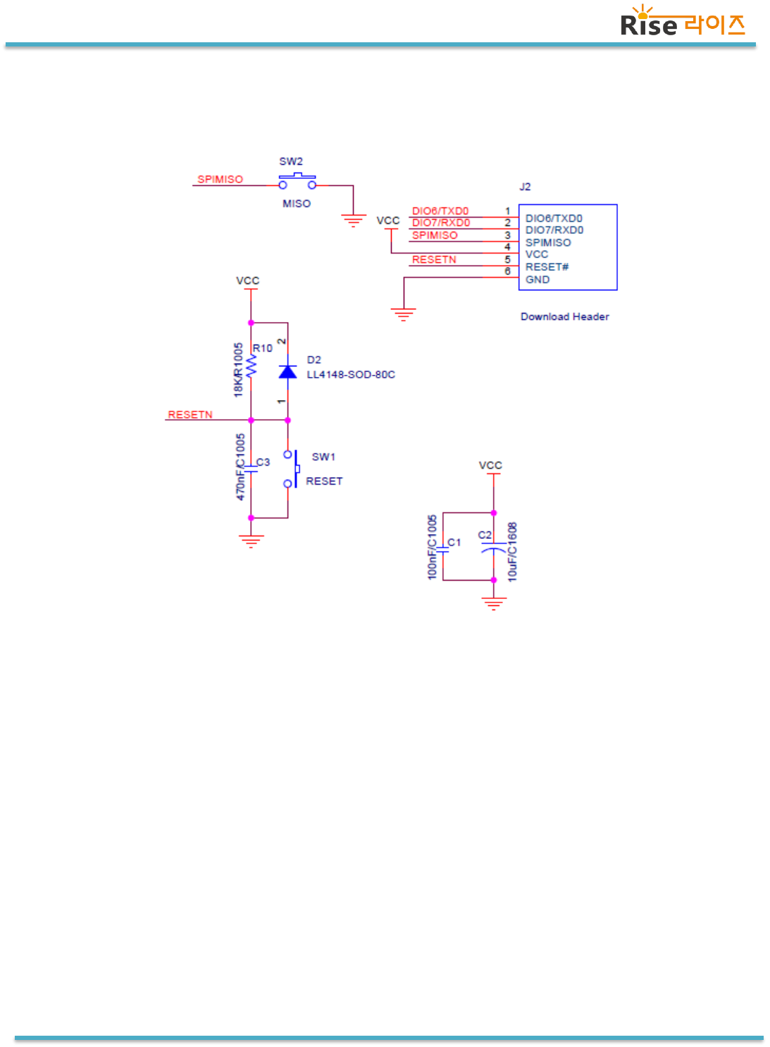
6. Module External Circuit for Programming
< Module External Circuit for Programming >
CMX-ZG03 Page 14
Appendix A Additional Information
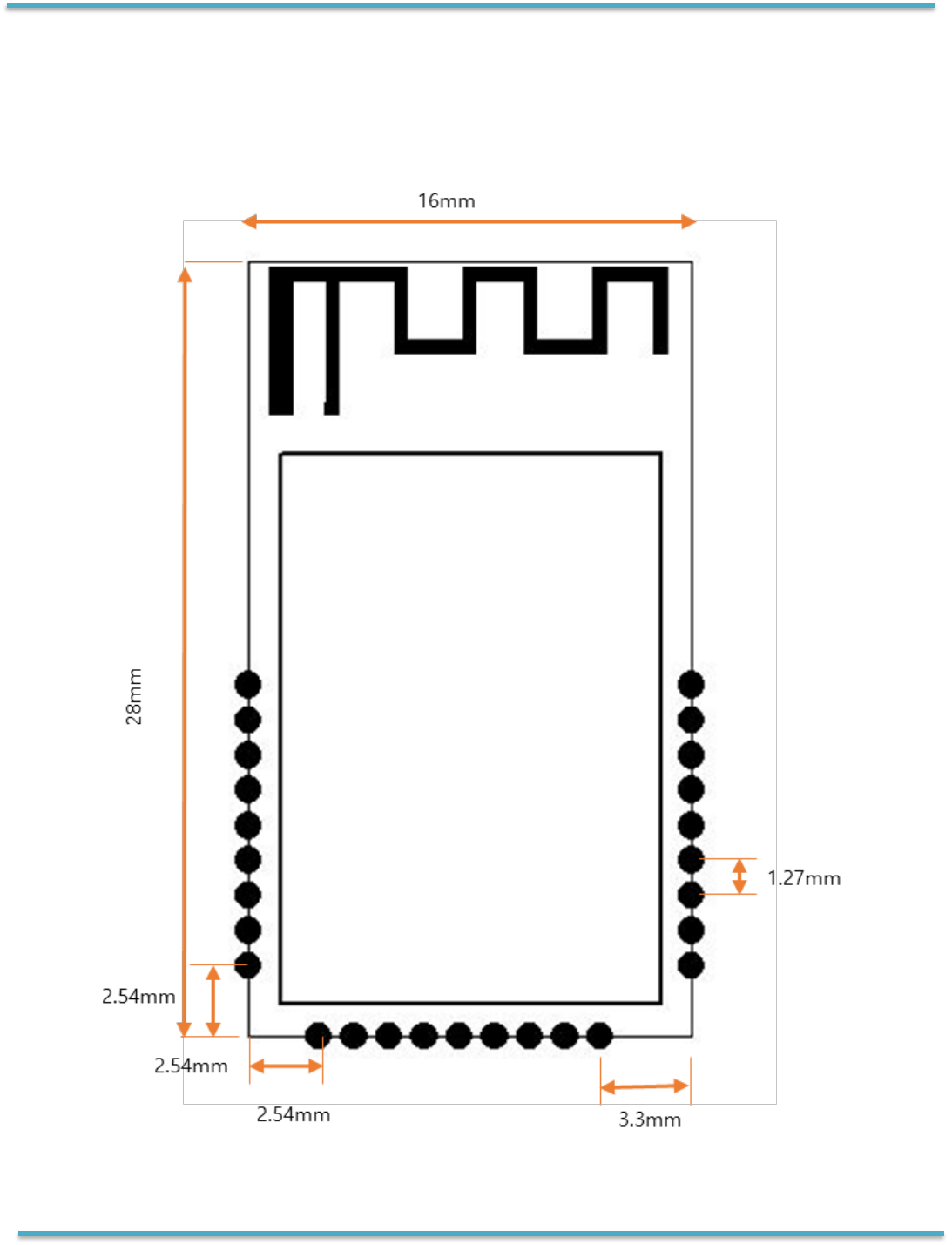
A.1. Outline Drawing : CMX-ZG03
CMX-ZG03 Page 15
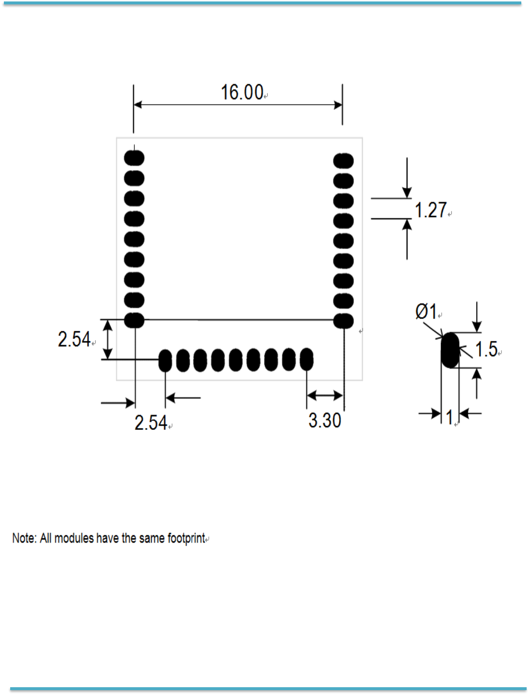
A.2. Module PCB Footprint

CMX-ZG03 Page 16
This eq
device,
user is
• Reori
•
•
receive
•
harmfu
FCC Infformation
pursuant t
reasonaa
equipmm
and usee
commuu
particullar installat
televisioo
ent or relo
Increaa
Connn
r is connec
Consuult the dea
Cautionn
Modific
cations not
the usee
FCC Coompliance
Operatii
interferr
Includinng interfer
approveed by the
equipmment under
text muu
Containn
to User
uipment haas been te
o
ble protecc
ent generaates, uses
d in accorrdance wit
nications. HH
ion. If this
n receptioo
encouragedd to try to
se the sepp
ect the equu
cate the re
aration be
ipment in
ted.
ler or an e
r’s authoritty to opera
on is subjee
l interferennce, and (2)
ence that mmay cause
eence that
mmanufactu
FCC rules.
st be placee
s Transmii
ssted and f
Part 15 oof the FCC
tion againsst harmful
owever, thhere is no
equipment
n, which caan be dete
ceiving an
tween the
tto an outl
xxperienced
expressly aapproved
Informatioon : This d
ct to the foollowing t
this devic
undesired
mmay cause
rrer could v
To satisfy
d on the eexterior of
tter Moduule FCC ID
iinterferenc
aand can raddiate radio
hh the instrucctions, ma
gguarantee
does caus
rmined by
correct thee interferen
ttenna.
equipment
eet on a circ
radio/TV t
bby the part
te the equi
ipment.
eevice comp
wwo conditi
ee must acc
ooperation
uundesired
ooid the use
FFCC exteri
tthe end pr
: CCECMX-ZG03
oound to commply with t
Rules. Thesse limits ar
yy cause har
tthat interf
e harmful i
turning th
ce by one
echnician f
yy responsib
llies with P
ooperation.
r’s authorit
ooduct.
ID : 22254-CMXZG03
ee designed
ee in a residential inst
ffrequency eenergy an
mful interf
eerence will
nterferenc
ee equipme
of the foll
and receivver.
uuit differentt from tha
or help.
oons: (1) This device m
eept any inteerference r
y To oper
oor labeling rrequireme
to provid
aallation. Thi
dd, if not ins
eerence to r
nnot occur i
ee to radio
nnt off and
oowing mea
le for compp
FCC Rulaart 15 of thee
aay not caus
eeceived, in
MModificationns not exp
aated the
nnts, the foll
he limits foor a Class BB digital
ee
ss
ttalled
adio
n a
oor
oon, the
ssures:
tt to which tthe
liance couuld void
ees.
e
c
cluding
rressly
oowing
The host of this equipment is limited to Commax Co., Ltd.
There are two models in which this module is installed.
FCC ID: CCECIP-700SW IC Number: 22254-CIP700SW Model Name: CIP-700SW
FCC ID: CCECIS-PM01 IC Number: 22254-CIS-PM01 Model Name: CIS-PM01

CMX-ZG03 Page 17
This d
The t1)
2)2)O
As lon
Howev
additio
digital
The O
to rem
IMPORR
certain
authori
produc
Manua
inform
user’s
shall in
CAUTIOON : This
conjuncction with
transmiitter devic
operatee this devic
This moo
IMPOR
FCC RFF
This eqquipment
uncontrr
minimuu
must nn
transmiitter
ransmitter
EM shall not s
changee.
gg as 2 con
eer, the OE
nal compli
ddevice emi
EEM integrat
oove or inst
TANT NO
laptop co
tt. In these
the endd
aation to th
mmanual of
ee. Any una
e.
dule is limmited to ins
TANT NOTTE:
Radiationn Exposure
complies
olled enviironment.
m distancee of 20 cen
ot be coo
eevice is inteended onl
module m
upply any
dditions abo
MM integrato
aance requir
sssions, PC
or is respo
aall module.
TTE:
In the
nnfiguration
oozation is n
circumstan
product (including t
ll Informatioo
clude all reequired reg
ddevice and iits antenn
aany other aantenna or
thorized
Statemen
with FCC
timeters b
-located oor operati
yy for OEM
aay not be
eevent that
longer coo
n To the EE
e end userr regardin
the end pproduct wh
ulatory inf
transmitte
tallation in fixed appl
tt:
RF radiat
TThis equippment sho
integrato
oottool or inf
vve are met, further tr
r is still ressponsible f
ements reqquired with
pperipheral rr
nsible for eensuring th
ss or co-locaation with
nsidered vv
ces, the OEE
he transmitt
nd User Thhe OEM in
gg how to i
ich integr
oormation/
aa(s) must noot be co-lo
rr.
mmodification
iion expos
uuld be ins
radiator aeetween the
nng in connjunction
cco-located ww
to the endd
aansmitter t
oor testing t
equiremenn
this modu
ts, etc.).
e end-user
tthese condiitions can
alid and thhe FCC ID c
M integratt
ter) and obbtaining a
ttegrator ha
nnstall or re
aates this m
wwarning as
cated or o
End serss
could voidd the user’
ications, and only installed Door Lock System
uure limits
rrs under thh
ith any ott
-user regaa
eest will not
nnot be met
aanother trannsmitter), t
an not be
or will be rr
s to be a
move this
odule. Th
sshow in thi
pperated in
cannot mooodify this
ss authority
set forth
talled and
nnd your boo
operated
dy.This tra
wwith any oother ant
her transmm
rding to RR
be require
hheir end-prroduct for
le installed (for exam
has no maa
(for exam
hhen the FC
used on th
esponsiblee for re-eva
sseparate FCC
wware not to
RF modul
e e end user
ss manual.
to
for an
with a
nnsmitter
eenna or
e followingg conditions:
itter or anttenna,
egulatory DDomain
dd.
aany
pple,
nual instruuction
pple
C
e final
C authorizz
luating
ation.
provide
ee in the
manual
This module can not be attached to other device without Door Lock System device.