CalAmp Wireless Networks 2424016-001 T-96SR Telemetry Transceiver/Modem User Manual Cover
CalAmp Wireless Networks Corporation T-96SR Telemetry Transceiver/Modem Cover
Contents
- 1. Transceiver manual
- 2. Modem manual
Transceiver manual

SYNTHESIZED VHF TELEMETRY UNIT
PART NO. 242-3422-XYZ
Third Printing
September 1998
Supersedes 001-3422-002 February 1998
Part No. 001-3422-003 U.S.A.

SYNTHESIZED VHF TELEMETRY UNIT
PART NO. 242-3422-XYZ
Copyright 1998 by the Johnson Data Telemetry Corporation.
The Johnson Data Telemetry Corporation designs and manufactures radios and radio modems to serve a wide variety of data
communication needs. The Johnson Data Telemetry Corporation produces equipment for the fixed data market including
SCADA systems for utilities, petrochemical, waste and fresh water management markets and RF boards for OEM applications
in the Radio Frequency Data Capture market.
DATA TELEMETRY PRODUCT WARRANTY
The manufacturer's warranty statement for this product is available from your product supplier or from the Johnson Data
Telemetry Corporation, 299 Johnson Avenue, PO Box 1733, Waseca, MN 56093-0833. Phone (507) 835-8819.
WARNING
This device complies with Part 15 of the FCC rules. Operation is subject to the condition that this device does not cause
harmful interference. In addition, changes or modification to this equipment not expressly approved by Johnson Data
Telemetry Corporation could void the user's authority to operate this equipment (FCC rules, 47CFR Part 15.19).
DO NOT allow the antenna to come close to or touch, the eyes, face, or any exposed body parts while the radio is transmitting.
DO NOT operate the radio near electrical blasting caps or in an explosive atmosphere.
DO NOT operate the radio unless all the radio frequency connectors are secure and any open connectors are properly
terminated.
DO NOT allow children to operate transmitter equipped radio equipment.
SAFETY INFORMATION
Proper operation of this radio will result in user exposure below the Occupational Safety and Health Act and Federal
Communication Commission limits.
The information in this document is subject to change without notice.
™ is a trademark of the Johnson Data Telemetry Corporation.

1
TABLE OF CONTENTS
1GENERAL INFORMATION
1.1 SCOPE OF MANUAL . . . . . . . . . . . . . . . . . . . . . . . . . . . . . . . . . . . . . . . . . . . . . . . . . . . . . . . . . . . . . . . . . . . . . . . 1-1
1.2 EQUIPMENT DESCRIPTION. . . . . . . . . . . . . . . . . . . . . . . . . . . . . . . . . . . . . . . . . . . . . . . . . . . . . . . . . . . . . . . . 1-1
GENERAL . . . . . . . . . . . . . . . . . . . . . . . . . . . . . . . . . . . . . . . . . . . . . . . . . . . . . . . . . . . . . . . . . . . . . . . . . . . . . . . . . 1-1
DL-3422 WITH LOADER BOARD . . . . . . . . . . . . . . . . . . . . . . . . . . . . . . . . . . . . . . . . . . . . . . . . . . . . . . . . . . . . . 1-1
DL-3422 WITH DL-3295 MODEM . . . . . . . . . . . . . . . . . . . . . . . . . . . . . . . . . . . . . . . . . . . . . . . . . . . . . . . . . . . . . 1-2
DM-3422 SYNTHESIZER PROGRAMMING. . . . . . . . . . . . . . . . . . . . . . . . . . . . . . . . . . . . . . . . . . . . . . . . . . . . . 1-2
1.3 TRANSCEIVER IDENTIFICATION . . . . . . . . . . . . . . . . . . . . . . . . . . . . . . . . . . . . . . . . . . . . . . . . . . . . . . . . . . 1-2
1.4 ACCESSORIES . . . . . . . . . . . . . . . . . . . . . . . . . . . . . . . . . . . . . . . . . . . . . . . . . . . . . . . . . . . . . . . . . . . . . . . . . . . . 1-2
1.5 PART NUMBER BREAKDOWN . . . . . . . . . . . . . . . . . . . . . . . . . . . . . . . . . . . . . . . . . . . . . . . . . . . . . . . . . . . . . 1-2
1.6 FACTORY CUSTOMER SERVICE . . . . . . . . . . . . . . . . . . . . . . . . . . . . . . . . . . . . . . . . . . . . . . . . . . . . . . . . . . . 1-2
1.7 PRODUCT WARRANTY . . . . . . . . . . . . . . . . . . . . . . . . . . . . . . . . . . . . . . . . . . . . . . . . . . . . . . . . . . . . . . . . . . . . 1-3
1.8 REPLACEMENT PARTS. . . . . . . . . . . . . . . . . . . . . . . . . . . . . . . . . . . . . . . . . . . . . . . . . . . . . . . . . . . . . . . . . . . . 1-3
1.9 FACTORY RETURNS . . . . . . . . . . . . . . . . . . . . . . . . . . . . . . . . . . . . . . . . . . . . . . . . . . . . . . . . . . . . . . . . . . . . . . 1-3
2INSTALLATION
2.1 PRE-INSTALLATION CHECKS . . . . . . . . . . . . . . . . . . . . . . . . . . . . . . . . . . . . . . . . . . . . . . . . . . . . . . . . . . . . . 2-1
2.2 INTERFACING WITH DATA EQUIPMENT . . . . . . . . . . . . . . . . . . . . . . . . . . . . . . . . . . . . . . . . . . . . . . . . . . . 2-1
DM-3422 (RF Board). . . . . . . . . . . . . . . . . . . . . . . . . . . . . . . . . . . . . . . . . . . . . . . . . . . . . . . . . . . . . . . . . . . . . . . . . 2-1
3PROGRAMMING
3.1 INTRODUCTION . . . . . . . . . . . . . . . . . . . . . . . . . . . . . . . . . . . . . . . . . . . . . . . . . . . . . . . . . . . . . . . . . . . . . . . . . . 3-1
3.2 DM3422 SYNTHESIZER DATA PROTOCOL . . . . . . . . . . . . . . . . . . . . . . . . . . . . . . . . . . . . . . . . . . . . . . . . . . 3-1
D-WORD . . . . . . . . . . . . . . . . . . . . . . . . . . . . . . . . . . . . . . . . . . . . . . . . . . . . . . . . . . . . . . . . . . . . . . . . . . . . . . . . . . 3-1
C-WORD . . . . . . . . . . . . . . . . . . . . . . . . . . . . . . . . . . . . . . . . . . . . . . . . . . . . . . . . . . . . . . . . . . . . . . . . . . . . . . . . . . 3-1
B-WORD . . . . . . . . . . . . . . . . . . . . . . . . . . . . . . . . . . . . . . . . . . . . . . . . . . . . . . . . . . . . . . . . . . . . . . . . . . . . . . . . . . 3-1
A-WORD . . . . . . . . . . . . . . . . . . . . . . . . . . . . . . . . . . . . . . . . . . . . . . . . . . . . . . . . . . . . . . . . . . . . . . . . . . . . . . . . . . 3-2
3.3 RECEIVE TO TRANSMIT SEQUENCE . . . . . . . . . . . . . . . . . . . . . . . . . . . . . . . . . . . . . . . . . . . . . . . . . . . . . . . 3-4
3.4 TRANSMIT TO RECEIVE SEQUENCE . . . . . . . . . . . . . . . . . . . . . . . . . . . . . . . . . . . . . . . . . . . . . . . . . . . . . . . 3-4
4CIRCUIT DESCRIPTION
4.1 GENERAL . . . . . . . . . . . . . . . . . . . . . . . . . . . . . . . . . . . . . . . . . . . . . . . . . . . . . . . . . . . . . . . . . . . . . . . . . . . . . . . . 4-1
INTRODUCTION . . . . . . . . . . . . . . . . . . . . . . . . . . . . . . . . . . . . . . . . . . . . . . . . . . . . . . . . . . . . . . . . . . . . . . . . . . . 4-1
SYNTHESIZER . . . . . . . . . . . . . . . . . . . . . . . . . . . . . . . . . . . . . . . . . . . . . . . . . . . . . . . . . . . . . . . . . . . . . . . . . . . . . 4-1
RECEIVER. . . . . . . . . . . . . . . . . . . . . . . . . . . . . . . . . . . . . . . . . . . . . . . . . . . . . . . . . . . . . . . . . . . . . . . . . . . . . . . . . 4-1
TRANSMITTER . . . . . . . . . . . . . . . . . . . . . . . . . . . . . . . . . . . . . . . . . . . . . . . . . . . . . . . . . . . . . . . . . . . . . . . . . . . . 4-1
LOADER BOARD. . . . . . . . . . . . . . . . . . . . . . . . . . . . . . . . . . . . . . . . . . . . . . . . . . . . . . . . . . . . . . . . . . . . . . . . . . . 4-1
4.2 SYNTHESIZER . . . . . . . . . . . . . . . . . . . . . . . . . . . . . . . . . . . . . . . . . . . . . . . . . . . . . . . . . . . . . . . . . . . . . . . . . . . . 4-1
VOLTAGE-CONTROLLED OSCILLATOR . . . . . . . . . . . . . . . . . . . . . . . . . . . . . . . . . . . . . . . . . . . . . . . . . . . . . . 4-3
VCO AND REFERENCE OSCILLATOR MODULATION . . . . . . . . . . . . . . . . . . . . . . . . . . . . . . . . . . . . . . . . . . 4-4
CASCODE AMPLIFIERS/VCO (Q871/Q872). . . . . . . . . . . . . . . . . . . . . . . . . . . . . . . . . . . . . . . . . . . . . . . . . . . . . 4-4
AMPLIFIER (Q882) . . . . . . . . . . . . . . . . . . . . . . . . . . . . . . . . . . . . . . . . . . . . . . . . . . . . . . . . . . . . . . . . . . . . . . . . . 4-4
VOLTAGE FILTER (Q901) . . . . . . . . . . . . . . . . . . . . . . . . . . . . . . . . . . . . . . . . . . . . . . . . . . . . . . . . . . . . . . . . . . . 4-4
VCO FREQUENCY SHIFT (Q841) . . . . . . . . . . . . . . . . . . . . . . . . . . . . . . . . . . . . . . . . . . . . . . . . . . . . . . . . . . . . . 4-4
SYNTHESIZER INTEGRATED CIRCUIT (U811) . . . . . . . . . . . . . . . . . . . . . . . . . . . . . . . . . . . . . . . . . . . . . . . . . 4-5
LOCK DETECT. . . . . . . . . . . . . . . . . . . . . . . . . . . . . . . . . . . . . . . . . . . . . . . . . . . . . . . . . . . . . . . . . . . . . . . . . . . . . 4-5
4.3 RECEIVER CIRCUIT DESCRIPTION . . . . . . . . . . . . . . . . . . . . . . . . . . . . . . . . . . . . . . . . . . . . . . . . . . . . . . . . 4-5
PRESELECTOR FILTER, RF AMPLIFIER (Q202) . . . . . . . . . . . . . . . . . . . . . . . . . . . . . . . . . . . . . . . . . . . . . . . . 4-5
MIXER (U231), AMPLIFIER (Q231). . . . . . . . . . . . . . . . . . . . . . . . . . . . . . . . . . . . . . . . . . . . . . . . . . . . . . . . . . . . 4-6
FIRST LO AMPLIFIER/BUFFER (Q301, Q302) . . . . . . . . . . . . . . . . . . . . . . . . . . . . . . . . . . . . . . . . . . . . . . . . . . . 4-6
CRYSTAL FILTER (Z231/Z232) . . . . . . . . . . . . . . . . . . . . . . . . . . . . . . . . . . . . . . . . . . . . . . . . . . . . . . . . . . . . . . . 4-6

1-1
Part No. 001-3422-003
SECTION 1
GENERAL INFORMATION
1.1 SCOPE OF MANUAL
This service manual contains alignment and service information for the Johnson Data Telemetry (JDT) DM-
3422 VHF Synthesized Telemetry Unit.
This manual concentrates on the RF section of the Data Link (DL) which may be paired with an internal
Loader board or 9600 baud Modem board.
Service manuals addressing items specific to the Loader board (Part No. 001-3240-003) and the Modem
board (Part No. 001-3295-002) should be referenced for the users specific configuration.
1.2 EQUIPMENT DESCRIPTION
1.2.1 GENERAL
The JDT DM-3422 is a synthesized data transceiver (transmitter and receiver) which operates in the 132-174
MHz VHF frequency range. Transmitter power output is 1-5 watts, 5W at 13.3V nominal. Operation is simplex or
half-duplex.
Versions of the DM-3422 covered in this manual are indicated in Section 1.5. The DM-3422 has a frequency
stability of ± 2.5 PPM (see Section 3) and is available with or without the Loader/Modem boards.
The number of channels that can be selected with the DM-3422 model is determined by the customer
supplied synthesizer loading circuitry. DL-3422 model can be supplied with the DL-3240 Loader board.
In addition to this VHF radio, JDT has a full line of radios and radio modems to meet wireless data
communication needs. Both OEM RF decks and complete FCC type approved radios and radio modems are
available from 132-174 MHz at VHF, 380-512 MHz at UHF, and 928-960 MHz at 900 MHz in both 5W and 2W
units (VHF and UHF). High Specification units are available to meet international requirements and bandwidths
to meet U.S.A. refarming requirements. To learn more about the other JDT products, call 1-800-992-7774 or
1-612-890-8155 to speak to a sales representative.

GENERAL INFORMATION
1-2
Part No. 001-3422-003
1.2.2 DL-3422 WITH LOADER BOARD
The DL-3422 includes the 8-channel Loader board (Part No. 023-3240-001), which performs synthesizer
loading through an RS-232 DB-9 interface. In addition, this board has circuitry which provides electronic control
of the following:
Transmit/Receive data conditioning and gating
Carrier Detect
Power Control
Preselector Tracking
Modulation Flatness
Audio/Data Filtering
Sleep/Wake-up to minimize current consumption
Diagnostics that includes:
Input Voltage Sense
Input Current Sense
Ambient Temperature Sense
RSSI Indicator (RSSI Sense)
Forward/Reverse Power Sense.
The gating circuits allow user selection of data filtering (standard or wide band) and also pre-emphasis/de-
emphasis to be enabled or disabled.
This board is programmed using an IBM PC or compatible computer and the Johnson Data Telemetry
programming software. Programming information is stored by an EEPROM on the Loader board. Refer to
Section 3 for programming information.
NOTE: The synthesizer must be loaded each time power is turned on. Therefore, one loader board or customer
supplied programming circuit is required for each data transceiver.
1.2.3 DL-3422 WITH DL-3295 MODEM
The DL-3496 modem (Part No. 023-3295-001) provides digital data transmission at data rates up to 9600
baud. The DL-3295 operates in Half-Duplex mode. However, two transceivers can be combined to provide Full-
Duplex operation. The user interface is a serial port through a 9-pin D-connector configurable to either RS-232 or
TTL signal levels. The data format is asynchronous with either 8 or 9 data bits. The modem can operate in either
standard DTE/DCE handshake p rotocol or in Data Activation mode which requires only receive and transmit data
lines. The baud rates are user selectable from 300 to 9600 baud.
1.2.4 DM-3422 SYNTHESIZER PROGRAMMING
The DM-3422, when used without the Universal Loader Board (Part No. 023-3240-001) requires customer
supplied circuitry to load the synthesizer with channel information. The protocol that this circuitry must follow is
described in Section 3.
GENERAL INFORMATION
1-3
Part No. 001-3422-003
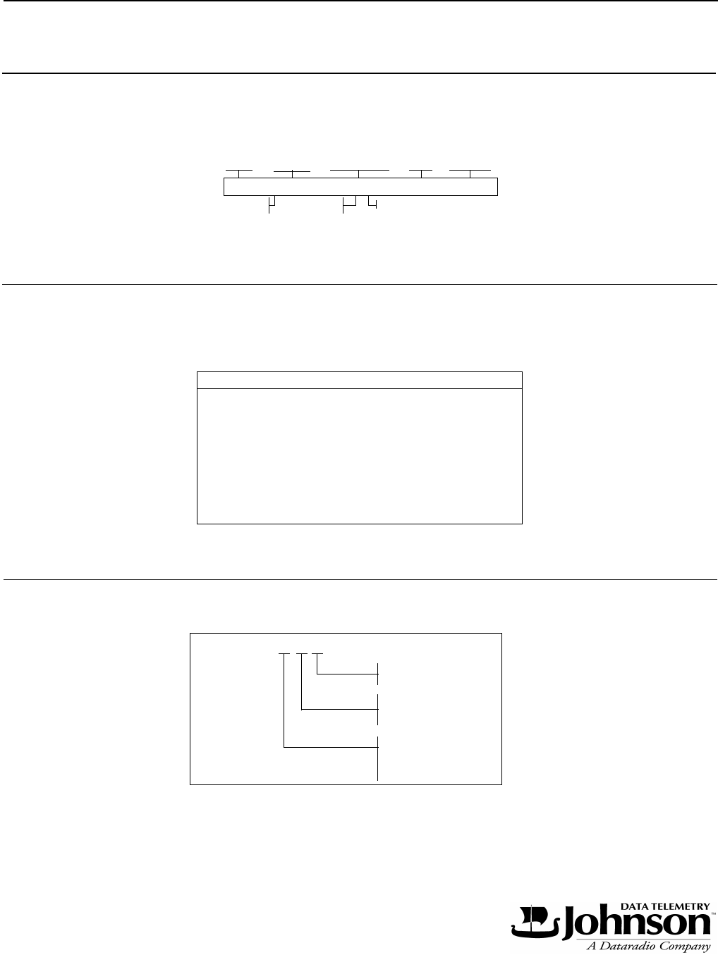
1.3 TRANSCEIVER IDENTIFICATION
The transceiver identification number is printed on a label that is affixed to the PC board. The following
information is contained in that number:
1.4 ACCESSORIES
Accessories available for the 3422 data transceiver are listed in Table 1-1.
1.5 PART NUMBER BREAKDOWN
The following is a breakdown of the part number used to identify this transceiver:
Table 1-1 ACCESSORIES
Accessory Part No.
DM-3422 Receive Test Filter 023-3472-040
DL-3295 Telemetry Modem 250-3295-001/101
DL-3240 Loader Kit 023-3240-001
DL-3295-001 Modem Kit 023-3295-001
DL-3282 Modem Kit 250-3282-001
DL-3240 Service Manual 001-3240-003
DL-3295 Service Manual 001-3295-002
3422 2A1 4 3 A12345
Model Revision
Letter
Ninth Digit
of PN
Manufacture
Date
Week No.
of Year Year
Plant Warranty
Number
242-3422 - X Y Z
0 = Base
1 = 15 kHz BW
4 = 132-150 MHz
5 = 150-174 MHz
3 = 30 kHz BW
2 = Portable
6 = 150-174 MHz*
* Refarming compatible (12.5 kHz only)

GENERAL INFORMATION
1-4
Part No. 001-3422-003
1.6 FACTORY CUSTOMER SERVICE
The Customer Service Department at JDT provides customer assistance on technical problems and the
availability of local and factory repair facilities. Customer Service hours are 7:30 a.m. - 4:30 p.m. Central Time,
Monday - Friday. From within the continental United States, the Customer Service Department can be reached at
this toll-free number
1-800-992-7774
When your call is answered at JDT, you will hear a brief message that contains the options: “1” for Sales, “2”
for Order Entry, “3” for Customer Service, “4” for Marketing, “7” for other issues, or “9” to repeat the message.
When you enter a first number of “3”, you may enter “1” for Technical Assistance, “2” for Product Repair or “3”
for Warranty. This number may be entered during or after the message using a tone-type telephone. If you have a
pulse-type telephone wait until the message is finished and an operator will come on the line to assist you. You can
enter the four digit extension number of the person that you want to reach at any time. If you are calling from
outside the continental United States, the Customer Service numbers are:
Customer Service Department - (507) 835-6911
FAX Machine - Cust Serv(507) 835-6969
You can contact the Customer Service Department by mail or email. Please include any information that may
help solve your problem. The mailing or email addresses are:
Johnson Data Telemetry Corporation
Customer Service Department
299 Johnson Avenue
P.O. Box 1733
Waseca, MN 56093-0514
support@johnsondata.com
1.7 PRODUCT WARRANTY
The warranty statement for this transceiver is available from the Warranty Department at JDT (see address or
telephone number in Section 1.6). The Warranty Department may also be contacted for Warranty Service Reports,
claim forms, or any questions concerning warranties or warranty service.
1.8 REPLACEMENT PARTS
Replacement parts can be ordered directly from the Service Parts Department. To order parts by phone, dial
the toll-free number and then enter “3” as described in Section 1.6. When ordering, please supply the part number
and quantity of each part ordered. JDT customers should give their account number.If there is uncertainty about the
part number, include the model number of the equipment the part is from (refer to Section 1.3).

GENERAL INFORMATION
1-5
Part No. 001-3422-003
You can send your order by mail or FAX (see Section 1.6 for mailing address). Mail orders should be sent to
the Service Parts Department.
FAX Machine - Sales (507) 835-6648
1.9 IF A PROBLEM ARISES...
JDT products are designed for long life and failure-free operation. If a problem arises, factory service is
available. Contact the Customer Service Department before returning equipment. A service representative may
suggest a solution eliminating the need to return equipment.
1.9.1 FACTORY REPAIR
Component level repair is not recommended on the DL-3422 Transceiver. Surface mount technology is used
to install many components that require specialized training and equipment to service board level components.
JDT’s factory is best equipped to diagnose problems and make component level repairs.
When returning equipment for repair, fill out a Factory Request Form for each unit to be repaired regardless
of warranty status. These forms are available free of charge by calling Customer Service (see Section 1.6).
Describe the problem in the space provided and note any prior physical damage to the equipment. Include a form
in the shipping container with each unit. Your phone number and contact name are important. There are times
when technicians have specific questions that need to be answered in order to identify the problem and repair the
equipment.
When returning equipment for repair, use a reference number on your paperwork in case you need to call
Customer Service about your unit. That number is referenced on the repair order to make it easier to locate your
unit in the lab.
Return authorization (RA) numbers are not necessary unless you have been given one by the Customer
Service Department. They require RA numbers for exchange units or if they want to be aware of a specific
problem. If you have been given an RA number, reference this number of the Factory Repair Request Form sent
with the unit. The repair lab will contact the Customer Service Department when the unit arrives.

GENERAL INFORMATION
1-6
Part No. 001-3422-003
3422 UHF SYNTHESIZED TELEMETRY UNIT SPECIFICATIONS
The following are general specifications intended for use in testing and servicing this transceiver. For current ad-
vertised specifications, refer to the specification sheet available from the Marketing Department. Specifications are
subject to change without notice.
GENERAL
Frequency Range 132-150 MHz/150-174 MHz
Frequency Control Synthesized
Channel Spacing 15/30 kHz
Mode of Operation Simplex or Half Duplex
Operating Voltage +13.3V DC nominal (10-16V DC operational)
Regulated Supply Voltages +5V DC ±5%
Transmit Enable 3-16V DC at 400 µA max
Receive Enable 3-16V DC ±5% at 400 µA nominal (400 µA during receive)
Transceiver Enable 3-16V DC at less than 400 µA
Power and Data Connector 14-pin in-line socket (Dupont 76308-14)
RF Input/Output SMA Jack (female)
Operating Temperature -30°C to +60°C (-22°F to +140°F)
Storage Temperature -40°C to +85°C (-40°F to +185°F)
Humidity 95% maximum RH at 40°C, non-condensing
Maximum Dimensions 4.585" L, 3.25" W, 2.212" H
FCC Compliance
DM-3422 Customer must apply
DL-3422 Part 90, Part 15
RECEIVER
Bandwidth 132-150 MHz: 18 MHz with electronic tuning
6 MHz without retuning from 132-150 MHz
150-174 MHz: 24 MHz with electronic tuning
6 MHz without retuning from 150-174 MHz
Frequency Stability ±2.5 PPM from -30°C to +60°C (-22°F to +140°F)
Sensitivity - 12 dB SINAD ≤ 0.35 µV, -116 dBm psophometrically weighted
RF Input Impedance 50 ohms
Selectivity -70 dB/-60 dB (tN/t/E) for 30 kHz, 60 dB/50 dB (tN/t/E) for 15 kHz
Spurious and Image Rejection -70 dB
Conducted Spurious Emissions < -57 dBm
Intermodulation -70 dB
FM Hum and Noise -45 dB, 30 kHz channels psophometrically weighted
-40 dB, 15 kHz channels psophometrically weighted
Receive Attack Time < 5 ms
Total Receive On Time 7 ms maximum
Audio
Distortion < 3% psophometrically weighted
Buffered Output Level 150 mV RMS nominal at 2.5V DC bias

GENERAL INFORMATION
1-7
Part No. 001-3422-003
Discriminator Output +1/-3 dB from DC to 5 kHz (reference to 1 kHz)(30 kHz BW) +1/-3 dB
from DC to 3.0 kHz 15 MHz BW
Output Bias 2.5V DC ±0.5 VDC
Output Impedance >10k ohms
Data Characteristics 4800/9600 BPS NRZ
RSSI 0.75V to 2.0V DC output from -120 to -60 dBm, attack time < 2 ms
TRANSMITTER
Frequency Stability ±2.5 PPM from -30°C to +60°C (-22°F to +140°F)
Bandwidth 132-150 MHz, 18 MHz without tuning
150-174 MHz, 24 MHz without tuning
Maximum System Deviation 5 kHz (30 kHz), 2.5 kHz (15 kHz)
Modulation FM/DC coupled
Input Bias 2.5V DC ±1% temperature compensated to ±100 mV. Supplied in Tx/Rx.
Input Impedance >40k ohms
Distortion < 3% at 60% of maximum system deviation, 1 kHz tone
Capability 1.8V P-P ±2 dB produces ±5 kHz deviation with a 1 kHz tone
Flatness ±2 dB, DC-5 kHz at 1 kHz (Programmable to ±0.5 dB with diagnostic
DAC)
RF Power Output 1-5W ±20% adjustable (5W at 13.3V nominal)
Deviation Symmetry 5%
RF Output Impedance 50 ohms
Duty Cycle 50% (30 sec. max transmit)
Transmitter Adjacent Power -70 dB
Intermodulation Attenuation -40 dB
Spurious and Harmonic FM -20 dBm max.
FM Hum and Noise -45 dB 30 kHz, -40 dB 15 kHz

GENERAL INFORMATION
1-8
Part No. 001-3422-003
This page left intentionally blank.

SECTION 2
2-1
Part No. 001-3422-003
INSTALLATION
1.1 PRE-INSTALLATION CHECKS
Field alignment should not be required before the 3422 is installed. However, it is still good practice to
check the performance to ensure that no damage occurred during shipment. Performance tests are located in
Section 6.2.
1.1 INTERFACING WITH DATA EQUIPMENT
1.1.1 DM-3422 (RF Board)
Connector J201 on the data transceiver PC board provides the interface with the data equipment. This is a
14-pin female connector with .025" square pins on 0.1" centers (Dupont 76308-114). The cable (Part No. 023-
3472-007) is not included with the data transceiver. An interface cable diagram and pin designations are shown
in Figure 2-1.
The following is a general description of the input and output signals on Transceiver Interface connector
J201.
Pin 1 (Ground) - Chassis ground.
Pin 2 (+13.3V DC) - Input, transceiver main power. Input range 10-16V DC with ±3 dB variation in output power.
Pin 3 (Tx En) - Input +3-16V DC. Enables transmit circuitry. ≤ 0.3V DC in Rx mode.
Pin 4 (Rx En) - Input +3-16V DC. Enables receive circuitry. ≤ 0.3 V DC in Tx mode.
Pin 5 (RF En) - Input +3-16V DC. Shuts down on-board regulators. To be used as a power save mode.
Pin 6 (Mod In) - Provides a response of ±2 dB from DC to 5 kHz across the RF band (referenced to
1 kHz). It is programmable to 1 dB with the diagnostic DAC. The modulation capability is 250 mV RMS
±3 dB that produces ±5 kHz deviation with a 1 kHz tone. When this input is used, a temperature compensated
2.5V DC bias is required as variations in voltage cause the frequency to change. The transceiver regulatory
compliance must be applied for with the customer supplied modulation limiting/filter circuit and chassis.
Pin 7 (Synth Lock) - Output from synthesizer lock detect circuit. Low (< 1V DC) = unlocked, high (>2.5V DC)
= locked.

INSTALLATION
-2
Part No. 001-3422-003
Pin 8 (Synth En) - TTL input. Latch enable signal for synthesizer. 250 ns min. for D, C and B words; 3 ms min.
for A0 word. A rising edge latches the data loaded into the synthesizer IC..
Pin 9 (Data) - TTL input. Serial data line used for programming the synthesizer and diagnostic functions.
Pin 10 (Synth Clock) - TTL input. Clock signal for serial data input on Pin 9. Data is valid on the rising edge. 1
MHz max. frequency.
Pin 11 (Diag En) - TTL input. Loads programmed DAC values into DAC (U911) for modulation adjust and power
set. Also provides the strobe signal for shift register (u901) for selecting Forward and Reverse power diagnostics.
250 ns min. activates on rising edge.
Pin 12 (RSSI) - Analog output (0.5-2V DC). The Receive Signal Strength Indicator output provides a voltage that
increases in proportion to the strength of the RF input signal.
Pin 13 (Demod) - Analog output. The Receiver Demod output level is 150 mV RMS with a modulation signal of 1
kHz at 60% of maximum deviation. The output is DC coupled and referenced to +2.5V DC. Load impedance should
be >10k ohms.
Pin 14 (Diag) - Analog Output. This pin is enabled by pin 11. When the Loader board is used it has the capability
to test the operating environment through diagnostics. The diagnostic capabilities are in Section 1.2.2

SECTION 3
3-1
Part No. 001-3422-003
PROGRAMMING
3.1 INTRODUCTION
The DL-3422 information in Section 3.2 describes synthesizer programming protocol. This information can
be used as a basis for designing the synthesizer programming hardware and software.
The DL-3422 VHF Transceiver uses a high performance Fractional-N Synthesizer and Voltage Controlled
Oscillator (VCO). The Fractional-N Synthesizer offers high frequency resolution, fast lock times, and improved
noise performance over conventional synthesis techniques. With conventional synthesizers, the phase detector
comparison frequency must be equal to the channel spacing because the main divider can only change in integer
steps. The channel spacing (resolution) of a Fractional-N synthesizer is a fraction of the comparison frequency.
With the Fractional-N synthesizer, the comparison frequency is increased to 5 or 8 times the channel step
frequency. The total loop division is reduced with a higher comparison frequency which improves phase noise.
Lock times are improved because the loop bandwidth can be wider.
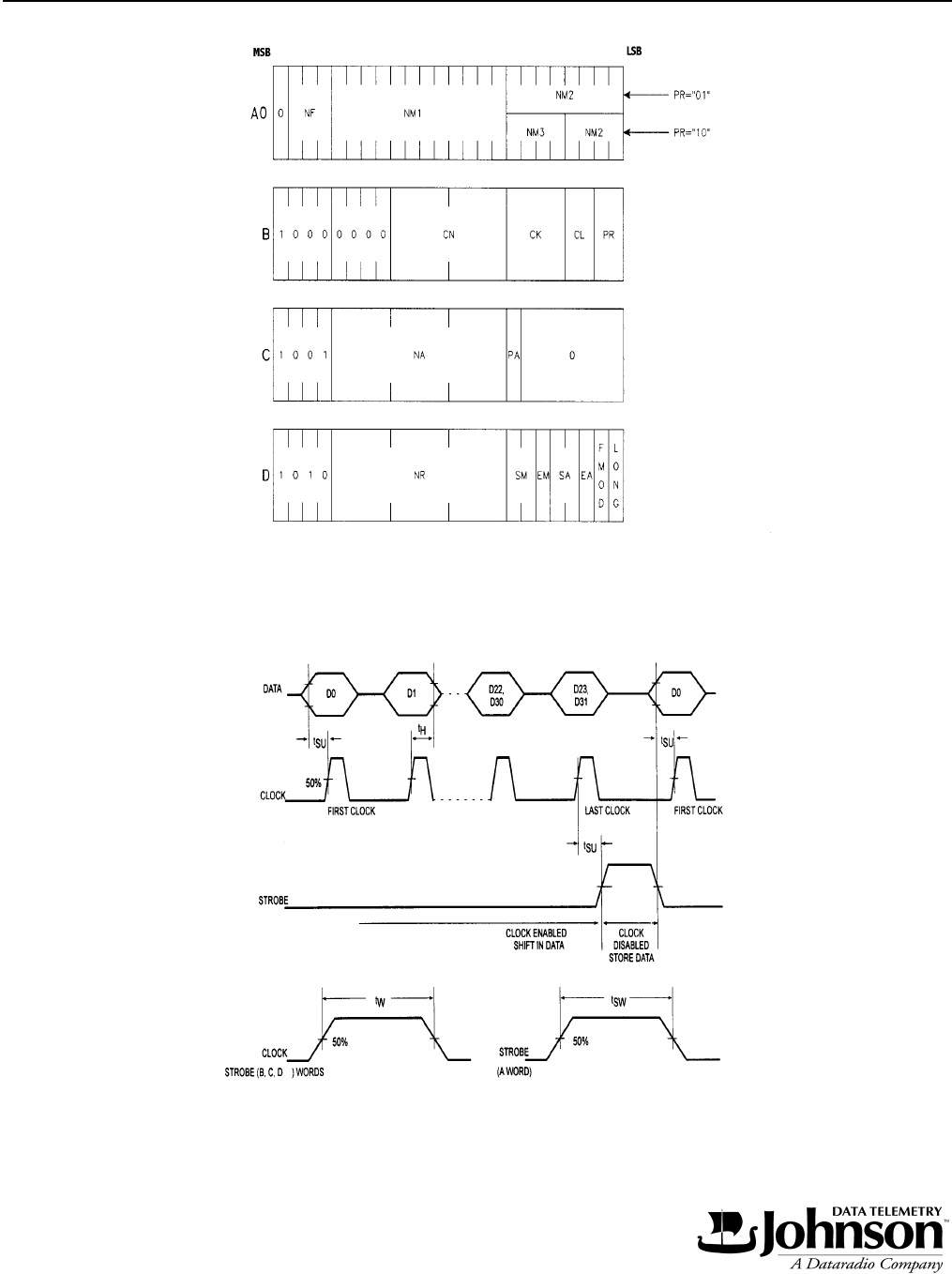
3.2 DL-3422 SYNTHESIZER DATA PROTOCOL
3.2.1 INTRODUCTION
Programming the SA-7025 synthesizer IC (U811) is accomplished via the 3-line bus; DATA, CLOCK, and
STROBE. Four 24 bit words (D, B, C, and A0) are required to load the synthesizer. The D, C, and B words
contain four address bits each; the A0 word has a 1 bit address. Synthesizer frequency acquisition is initiated
when the A0 word is loaded. We recommend using modulus 3 and sending the D, B, C, and A0 words for each
synthesizer load (LONG load). When the STROBE = low, the clock driver is enabled and the DATA is clocked
into the shift registers on the positive edges of the CLOCK. When STROBE = high, the clock is disabled and the
data in the shift registers remain stable. The DATA is latched into different working (or temporary) registers
depending on the address bit(s). In order to fully program the synthesizer, all four words must be sent with the
A0 word sent last. Refer to Table 3-1 and Figure 3-3 for data format information.
3.2.2 PROGRAMMING SYNTHESIZER PARAMETERS
The DL-3422- RF Board is available in three frequency ranges, 132-150 MHz (Band 4), 150-174 MHz
(Band 5), and 150-174 MHz (Band 6). Band 6 was designed to be compatible with the FCC’s refarmed VHF
band plan therefore, 2.5 kHz channel resolution is used. The Band 4 and 5 versions can be programmed for 5,
6.25, and 7.5 kHz steps depending on user requirements.
PROGRAMMING
3-2
Part No. 001-3422-003
Table 3-1 Programming Function Table
Symbol Bits Function
NM1 12 Number of main divider cycles when prescaler modulus = 64*
NM2 8 if PR = “01”
4 if PR = “10” Number of main divider cycles when prescaler modulus = 65*
NM3 4 if PR = “10” Number of main divider cycles when prescaler modulus = 72*
PR 2Prescaler type in use
PR = “01”: modulus 2 prescaler (64/65)
PR = “10”: modulus 3 prescaler (64/65/72)
NF 3Fractional-N increment
FMOD 1Fractional-N modulus selection flag
“1”: modulo 8
“0”: modulo 5
LONG 1A word format selection flag
“0”: 24 bit A0 format
“1”: 32 bit A1 format
CN 8Binary current setting factor for main charge pumps
CL 2Binary acceleration factor for proportional charge pump current
CK 4Binary acceleration factor for integral charge pump current
EM 1Main divider enable flag
EA 1Auxiliary divider enable flag
SM 2Reference select for main phase detector
SA 2Reference select for auxiliary phase detector
NR 12 Reference divider ratio
NA 12 Auxiliary divider ratio
PA 1Auxiliary prescaler mode:
PA = “0”: divide by 4
PA = “1”: divide by 1
* Not including reset cycles and Fractional-N effects.
PROGRAMMING
3-3
Part No. 001-3422-003
Figure 3-2 Serial Input Word Format
Figure 3-3 Serial Input Timing Sequence
PROGRAMMING
3-4
Part No. 001-3422-003
3.2.3 GENERAL RADIO PROGRAMMING PARAMETERS
Receive Bandwidth: 132-150 MHz (Band 4), 150-174 MHz (Band 5, 6)
Transmit Bandwidth: 132-150 MHz (Band 4), 150-174 MHz (Band 5, 6)
First IF: 21.45 MHz
Second IF: 450.0 kHz
First LO injection: 153.45 to 195.45 (high side injection)
Second LO injection (LO2): 21.9 MHz (high side injection)
TCXO Frequency (FREF): 14.85 MHz (Band 4, 5), 17.50 MHz (Band 6)
Resolution: 7.5, 6.25, 5.0 kHz (Band 4, 5), 2.5 kHz (Band 6)
Comparison Frequency (FCM): 37.5, 50, 25 kHz (Band 4, 5), 20 kHz (Band 6)
Synthesizer IC: Phillips SA7025A
D-WORD
The D-Word programs the Reference dividers, sets enable flags for the main auxiliary phase detectors, and
sets the modulus.
NR = 396 (for 7.5 kHz resolution)
NR = 297 (for 6.25 kHz resolution)
NR = 594 (for 5.0 kHz resolution)
NR = 875 (for 2.5 kHz resolution) NOTE: applies to Band 6 only.
SM = 00
EM = 1
EA = 1
SA = 00
FMOD = 0 (for 7.5 and 5.0 kHz resolution) Modulo 5
FMOD = 1 (for 6.25 and 2.5 kHz resolution) Modulo 8
LONG = 0
Where: FCM = FREF ÷ NR and RESOLUTION = FCM ÷ FMOD
Table 3-2 Serial Interface Specifications
Symbol Parameter Test Conditions Limits
MIN TYP MAX Units
fCLOCK Clock Frequency 10 MHz
tSU Set-up time: DATA to CLOCK
CLOCK to STROBE
30 ns
tHHold Time: CLOCK to DATA 30 ns
tWPulse width; CLOCK
Pulse width; STROBE B, C, D words
30
30 ns
tSW Pulse width; STROBE
A word, PR = "01"
A word, PR = "10"
1 . (NM2 . 65) + tW
fVCO
1 . [(NM2 . 65) + (NM3 + 1 . 72] + tW
fVCO
ns
PROGRAMMING
3-5
Part No. 001-3422-003
C-WORD
The C-Word programs the Auxiliary (2nd LO injection frequency) and selects auxiliary preselector mode.
PA = 1
NA = 584 (for 7.5 kHz resolution)
NA = 438 (for 6.25 kHz resolution
NA = 876 (for 5.0 kHz resolution)
NA = 1095 (for 2.5 kHz resolution) NOTE: applies to Band 6 only.
Where: NA = LO2 ÷ FCM
B-WORD
The B-Word programs the Fractional-N charge pump current factor (CN), the binary acceleration factors (CL/
CK) and the prescaler modulus. The value of CN should be interpolated for frequencies between the band edges.
The recommended range of CN provides the necessary spurious rejection required to meet the adjacent channel
specifications across the band.
Table 3-3 CN VALUES VERSUS FREQUENCY AND BAND
Band 4 (132-150 MHz) Band 5 (150-174 MHz) Band 6 (150-174 MHz)
Frequency Transmit Receive Frequency Transmit Receive Frequency Transmit Receive
MHz CN CN MHz CN CN MHz CN CN
132 78 91 150 150 82 95
150 88 101 174 174 93 106
CK = 0000
CL = 00
PR = 10 (selects modulus 3 prescaler)

PROGRAMMING
3-6
Part No. 001-3422-003
THE A0-WORD
The A0 Word is sent last. the A0 word contains the programming information for the main dividers. The A0
word consists of four divider parameters, NM1, NM2, NM3, and NF described below. After clocking the A0 word,
the STROBE line is held high for approximately 3 ms to place the synthesizer in “speed-up” mode to decrease lock
times.
NF: Fractional-N increment (3 bits, depends on channel selection and FMOD)
NM1: Number of main divide cycles when prescaler modulus = 64 (12 bits)
NM2: Number of main divide cycles when prescaler modulus = 65 (4 bits, PR = 10).
NM3: Number of main divide cycles when modulus = 72 (4 bits, PR = 10)
The Fractional-N increment (NF) is a 3 bit word that is used to program the synthesizer to channels
(frequency steps) that are less then, or a fraction of, the comparison frequency (FCM).
3.2.4 LOCK DETECT
The LOCK detect output from the synthesizer is available for monitoring on J201 pin 7. The LOCK output is
high when the main and auxiliary phase detectors indicate a lock condition. The lock condition is defined as less
then +1 cycle on the reference input to the synthesizer IC. The LOCK detect line should be monitored to verify a
locked condition before transmitting.
EXAMPLE CALCULATION
Program a Band 6 radio to receive at 151.0175 MHz
D-Word Calculation:
NR = 875 (Decimal)
SM = 00
EM = 1
EA = 1
SA = 00
FMOD = 1
LONG = 0
D-Word (Hex) = A3 6B 26

PROGRAMMING
3-7
Part No. 001-3422-003
C-Word calculation:
NA = 1095 (Decimal)
PA = 1
C-Word (Hex) = 94 47 80
B-Word calculation:
CN = 95 (Decimal from Table 3-3)
CK = 0000
CL = 00
PR = 10
B-Word (Hex) = 80 5F 2
A0-Word calculation:
When the D-Word is programmed with FMOD = 8 and NR = 875 as described above, the fractional increment
resolution is FCM ÷ FMOD = 20 kHz ÷ 8 = 2.5 kHz.
Where FCM = FREF ÷ NR = 17.5 MHz ÷ 875 = 20 kHz.
The total division ratio from the prescaler to the phase detector (with PR= “10”) is expressed as:
N = (NM1 + 2) x 64 + NM2 x 65 + (NM3 + 1) x 72
N’ = (NM1 + 1) x 64 + (NM2 + 1) x 65 + (NM3 + 1) x 72*
*When the fractional accumulator overflows the prescaler ratio = 65 x (64 + 1) and the total division ratio is
N’ = N + 1.
In the receive mode, the synthesizer is programmed to the 1st LO injection frequency which is 21.45 MHz
above the receive frequency (high side injection).
For this example, LO = 151.0175 + 21.45 MHz = 172.4675 MHz
N = LO ÷ FCM = 172.4675 ÷ .02 = 8623 {Integer part}
NM3 = [ INT{64 x FRAC {N ÷ 64} ÷ FMOD}] -1
= INT { (64 x 0.734375) ÷ 8} -1
= 5 - 1 = 4
NM2 = FMOD x FRAC {N ÷ FMOD}
= 8 x FRAC {1023 ÷ 8}
= 8 x 0.875
= 7

PROGRAMMING
3-8
Part No. 001-3422-003
NM1 = INT {N ÷ 64} - NM2 - NM3 - 3
= 134 - 7 - 4 - 3
= 120
NF = FRAC {LO ÷ FCM} x FMOD
= FRAC {171.4625 ÷ 0.02} x 8
= 0.125 x 8
= 3
Where INT = Integer Part
FRAC = Fractional Part
PROGRAMMING
3-9
Part No. 001-3422-003
3.3 RECEIVE TO TRANSMIT SEQUENCE
1. Load the synthesizer (D, C, B and A0 words).
2. The RX Enable (J201, pin 4) is changed from a logic high to logic low after the last bit of the A0 Word is sent.
3. The SYNTH ENABLE (SYNTH_EN) should be held in a high state for 3 milliseconds after the A0 Word is sent.
This puts the synthesizer in a temporary “speedup mode” which improves lock times. Then, the SYNTH_EN is
returned to a low state.
4. After the A0 Word is strobed in, wait 7ms (worst case) before applying a logic high to the 7.5 TX 1 line (J201,
pin 3). This allows the synthesizer to attain lock. NOTE: The lock detect line (J201, pin 7) should be monitored
and in a lock (logic high) state before enabling the transmitter.
1 A "ramp-up/-down" circuit should be employed on the Loader to minimize adjacent channel interference caused
by the spectral spreading that occurs when a transmitter is suddenly switched on or off. The ramped voltage is
applied to the 7.5 TX line (J201, pin 3). The ramp should be approximately 3 ms.
Figure 3-4 Rx to Tx TIMING DIAGRAM
“D WORD” “B WORD” “A” WORD
PROGRAMMING
3-10
Part No. 001-3422-003
3.4 TRANSMIT TO RECEIVE SEQUENCE
1. Unkey the transmitter by bringing the 7.5 TX low.
2. Allow 3 ms for “ramp-down” 1 after the 7.5 TX is brought low.
3. Apply a logic high to the RX Enable line.
4. Load the synthesizer receive frequency. The SYNTH Enable line should be held high for 3 ms on the last word
to place the synthesizer in speedup mode for faster lock times. The SYNTH Enable line should then be returned
to logic low.
5. After the A0-Word is strobed in, the synthesizer will initiate frequency acquisition. The Lock Detect line (J201,
pin 7) should be monitored and in a lock (logic high) state before valid receive operation.
1 A “ramp-up/-down” circuit should be employed on the Loader to minimize adjacent channel interference
caused by the spectral spreading that occurs when a transmitter is suddenly switched on or off. The ramped voltage
is applied to the 7.5 TX line (J201, pin 3). The ramp should be approximately 3 ms.

-
June 1997
Figure 3-5 TX TO RX TIMING DIAGRAM

SECTION 4
4-1
Part No. 001-3422-003
CIRCUIT DESCRIPTION
4.1 GENERAL
4.1.1 INTRODUCTION
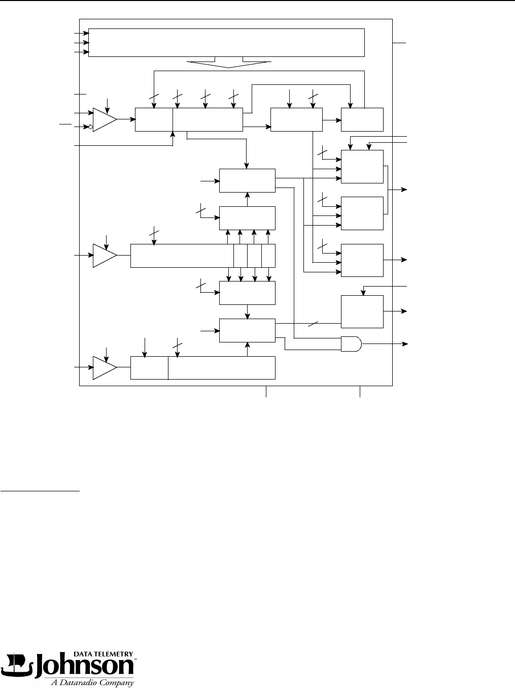
The main subassemblies of this transceiver are the RF board, VCO board, TCXO and Loader board. A
block diagram of the transceiver is located in Figure 4-1.
The 3422 is available with a reference oscillator stability of ±2.5 PPM. The TCXO (Temperature
Compensated Crystal Oscillator) is soldered directly to the RF board. The TCXO is not
serviceable.
4.1.2 SYNTHESIZER
The VCO (voltage-controlled oscillator) output signal is the receiver first injection frequency in the Receive
mode and the transmit frequency in the Transmit mode. The first injection frequency is 21.45 MHz above the
receive frequency. The frequency of this oscillator is controlled by a DC voltage produced by the phase detector
in synthesizer chip U811.
Channels are selected by programming counters in U811 to divide by a certain number. This programming
is performed over a serial bus formed by the Synth Clock, Synth Enable, and Synth Data pins of J201. This
programming is performed by the Loader board or user supplied hardware and software (see Section 3).
The frequency stability of the synthesizer in both the receive and transmit modes is established by the
stability of the reference oscillator described in the preceding section. These oscillators are stable over a
temperature range of -30° to +60° C (-22° to +140° F).
Table 4-1 Reference Frequency
Band Frequency
Band 6 17.5 MHz
Band 5 14.85 MHz
Band 4 14.85 MHz

CIRCUIT DESCRIPTION
4-2
Part No. 001-3422-003
4.1.3 RECEIVER
The receiver is a double-conversion type with intermediate frequencies of 21.45 MHz / 450 kHz. Varactor
tuned LC bandpass filters reject the image, half IF, injection, and other unwanted frequencies. A four-pole crystal
filter enhances receiver selectivity.
4.1.4 TRANSMITTER
The transmitter produces a nominal RF power output of 5W at 13.3V DC, adjustable down to 1W. Frequency
modulation of the transmit signal occurs in the synthesizer. Transmit audio processing circuitry is contained in the
Loader board or customer-supplied equipment.
4.1.5 LOADER BOARD
The Loader board, Part No. 023-3240-330, is a plug-in circuit board used to load the synthesizer with a
desired frequency and filters data/audio to and from the user interface connector. The Loader board is programmed
by a personal computer and software.
4.2 SYNTHESIZER
A block diagram of the transceiver is shown in Figure 4-1 and a block diagram of Synthesizer IC U811 is
shown in Figure 4-2. The synthesizer output signal (produced by a VCO) is controlled by a DC voltage produced
by the phase detector in U811. The phase detector senses the phase and frequency of the two input signals and
causes the VCO control voltage to increase or decrease (if they are not the same). The VCO is then "locked" on
frequency.
Synthesizer programming provides the data necessary for the internal prescaler and counters. One input
signal is the reference frequency. This frequency is produced by the 14.85 MHz reference oscillator (TCXO). The
other input signal is the VCO frequency.
CIRCUIT DESCRIPTION
4-3
Part No. 001-3422-003
Figure 4-1 Transceiver Block Diagram
RF AMP
MIXER
CRYSTAL FILTER
PREDRIVER ANTENNA
SWITCH
RX AUDIO
VCO
T/R PS
SYNTHESIZER
VCO
RSSI
LOW-PASS
FILTER
RF OUT
RF BPF RF BPF IF / 450 kHz FILTER
1st LO AMP
CLV
BUFFER/AMPLIFIER
RSSI
RX OUT
TX IN Y801
TCXO
MOD INPUT
MOD ADJUST
SYNTH OUT
RF IN
U241
TRANSMITTER
RECEIVER
+13.6V
+4.6V
U581A
U581B
PWR SET
DIAG
DIAG EN
MOD ADJ
DIAG DIAG EN
TX EN +9V TX
RX EN
+13.6V
SWITCHED
CLOCK
DATA
ENABLE
LOCK
Q122
Q121
Q801
TEST
-2.0V
Q501
Q123
+5V DC
SHUTDOWN
Q511
Q531/U111C
CR561/562
V FWD
V REV U913C
U911
U912
Q131/U131
U141 +9.6V
+5.5V
Q201/Q202
U531
Q301/Q302
Q231/Q232 21.45 MHz
Z231/Z232
Q251
Q101/Q102
U111A/B/D
Q124
Q871/Q872 Q881/Q882
Q171, Q172, Q173
Q173, Q841
Q842, Q901
AUX IN
U811
Q701
CR281/CR282 CR281/CR282
CR251
PHP
PHA
U801
CLOCK
DATA
U913A
U831B U913B
CIRCUIT DESCRIPTION
4-4
Part No. 001-3422-003
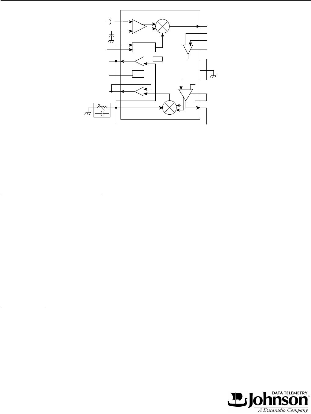
Figure 4-2 U811 Synthesizer Block Diagram
4.2.1 VOLTAGE-CONTROLLED OSCILLATOR
Oscillator (Q872)
The VCO is formed by Q872, several capacitors and varactor diodes, and air wound coil L872. It oscillates at
the transmit frequency in transmit mode and first injection frequency in the receive mode
(132-174 MHz in transmit and 153.45-195.45 MHz in receive).
Biasing of Q872 is provided by R873, R874 and R876. An AC voltage divider formed by C872, C874 and
C875 initiates and maintains oscillation and also matches Q872 to the tank circuit. Air wound inductor L872 is
grounded at one end to provide shunt inductance to the tank circuit.
CLOCK
DATA
STROBE
Vss
RFIN
RFIN
64/65/72
PRESCALER MAIN DIVIDERS
EM FB 2 2 12 8
PR NM1 NM3
NM2
FRACTIONAL
ACCUMULATOR
PRESCALER
MODULUS
CONTROL
3
FMOD NF FB
SERIAL INPUT + PROGRAM LATCHES VDD
TEST
IN
REF
EM+EA
REFERENCE DIVIDER +2 +2 +2
MAIN
MAIN
PHASE
DETECTOR
REFERENCE
SELECT
2
SM
EM
REFERENCE
SELECT
2
SA
SECONDARY
PHASE
DETECTOR
EA AUXILIARY
IN
EA
AUX
12
NR
12
NAPA
AUXILIARY DIVIDER
PRESCALER
1/4
NORMAL
OUTPUT
CHARGE
PUMP
OUTPUT
CHARGE
PUMP
SPEED-UP
OUTPUT
CHARGE
PUMP
INTEGRAL
OUTPUT
CHARGE
PUMP
AUXILIARY
CN
8
CL
2
CK
4
2
VSSA
VDDA
LOCK
PHA
RA
PHI
PHP
RN
RF

CIRCUIT DESCRIPTION
4-5
Part No. 001-3422-003
Frequency Control and Modulation
The VCO frequency is controlled in part by DC voltage across varactor diodes CR852, CR853 and CR854.
As voltage across a reverse-biased varactor diode increases, its capacitance decreases. Therefore, VCO frequency
increases as the control voltage increases. CR852/CR853 and CR854 are paralleled varactors to divide the
capacitance and improve linearity. The varactors CR852/CR853 are biased at -2.0V so the control line voltage can
operate closer to ground. CR854 is pin shifted in when transmitting to increase the VCO gain in transmit. The
control line is isolated from tank circuit RF by choke L852/L853. The amount of frequency change produced by
CR852/CR853/CR854 is controlled by series capacitor C854.
The -2.0V applied to the VCO is derived from the TCXO frequency that is amplified by Q902, rectified by
CR902 and filtered by C912, C917, C918 and C920 and loaded by resistor R919 on the RF board.
The VCO frequency is modulated using a similar method. The transmit audio/data signal from J201, pin 6 is
applied across varactor diode CR861 which varies the VCO frequency at an audio rate. Series capacitors C855/
C856 set the amount of deviation produced along with CR862 and C865. R863 provides a DC ground on the
anodes of CR861/CR862, and isolation is provided by R862 and C863.
The DC voltage across CR862 provides compensation to keep modulation relatively flat over the entire
bandwidth of the VCO. This compensation is required because modulation tends to increase as the VCO
frequency gets higher (capacitance of CR852/CR853/CR855 gets lower). CR862 also balances the modulation
signals applied to the VCO and TCXO. The D/A Converter U911 can be programmed to apply a compensating
voltage to CR862 to adjust the modulation sensitivity between the TCXO and VCO.
The DC voltage applied across CR862 comes from the modulation adjust control R827 on the RF board.
R826 applies a DC biasing voltage to CR862; C821 provides DC blocking. RF isolation is provided by C865 and
R862.
4.2.2 VCO AND REFERENCE OSCILLATOR MODULATION
Both the VCO and reference oscillator (TCXO) are modulated in order to achieve the required frequency
response. If only the VCO was modulated, the phase detector in U811 would sense the frequency change and
increase or decrease the VCO control voltage to counteract the change (especially at the lower audio frequencies).
If only the reference oscillator frequency is modulated, the VCO frequency would not change fast enough
(especially at the higher audio frequencies). Modulating both VCO and reference oscillators produces a flat audio
response. Potentiometers R825 and R827 set the VCO modulation sensitivity so that it is equal to the reference
oscillator modulation
sensitivity.

CIRCUIT DESCRIPTION
4-6
Part No. 001-3422-003
4.2.3 CASCODE AMPLIFIERS/VCO (Q871/Q872)
The output signal on the collector of Q871 is coupled to buffer amplifier Q872 which forms a cascade
amplifier. This is a shared-bias amplifier which provides amplification and also isolation from the stages that
follow. The signal is coupled and matched from the collector of Q872 through inductors and capacitors and a
T-pad to amplifier Q882.
4.2.4 AMPLIFIER (Q882)
Amplifier Q882 provides final amplification of the VCO signal. Bias for Q882 is provided by Q881 and
several resistors. Matching to the transmitter and receive first injection is provided by L891 and C892. A 6 dB
T-pad is used to isolate the transmitter and receive first injection.
4.2.5 VOLTAGE FILTER (Q901)
Q901 on the RF board is a capacitance multiplier to provide filtering of the 8.6V supply to the VCO. R901
provides transistor bias and C901 provides the capacitance that is multiplied. If a noise pulse or other voltage
change appears on the collector, the base voltage does not change significantly because of C901. Therefore, base
current does not change and transistor current remains constant. CR901 decreases the charge time of C901 when
power is turned on. This shortens the start-up time of the VCO. C902 and C903 are RF decoupling capacitors.
4.2.6 VCO FREQUENCY SHIFT (Q841)
The VCO must be capable of producing frequencies from approximately 132-195.45 MHz to produce the
required receive injection and transmit frequencies. If this large of a shift was achieved by varying the VCO
control voltage, the VCO gain would be undesirably high. Therefore, capacitance is switched in and out of the
tank circuit to provide a coarse shift in frequency.
This switching is controlled by the T/R pin shift (RX_EN) on J201, pin 4, Q841/Q842 and pin diode CR851.
When a pin diode is forward biased, it presents a very low impedance to RF; and when it is reverse biased, it
presents a very high impedance. The capacitive leg is switched in when in transmit and out when in receive.
When J201, pin 4 is high in receive (+5V), Q173 is turned on and the collector voltage goes low. A low on
the base of Q172 turns the transistor on and the regulated +9.6V on the emitter is on the collector for the receive
circuitry. Q171 applies a low on the base of Q841, the transistor is off and the collector is high. With a high on the
base of Q842 and a low on the emitter, this reverse biases CR851 for a high impedance.
The capacitive leg on the VCO board is formed by C852, CR851 and C853. When J201, pin 4 is low in
transmit, Q842 is turned on and a high is on the emitter, Q171 is turned off and the collector voltage goes high. A
low on the base of Q173 turns the transistor off and the regulated +9.6V is removed from the receive circuitry.
With a high on the base of Q841 the transistor is on and the collector is low. With a low on the collector of Q842
and a high on the emitter, this forward biases CR851 and provides an RF ground through C852 and C853 is
effectively connected to the tank circuit. This decreases the resonant frequency of the tank circuit.

CIRCUIT DESCRIPTION
4-7
Part No. 001-3422-003
4.2.7 SYNTHESIZER INTEGRATED CIRCUIT (U811)
Introduction
Synthesizer chip U811 is shown in Figure 4-2. This device contains the following circuits: R (reference),
Fractional-N, NM1, NM2 and NM3; phase and lock detectors, prescaler and counter programming circuitry. The
basic operation was described in Section 4.2.1.
Channel Programming
Frequencies are selected by programming the R, Fractional-N, NM1, NM2 and NM3 in U811 to divide by a
certain number. These counters are programmed by Loader board or a user supplied programming circuit. More
information on programming is located in Section 3.
As previously stated, the counter divide numbers are chosen so that when the VCO is oscillating on the
correct frequency, the VCO-derived input to the phase detector is the same frequency as the reference oscillator-
derived frequency.
The VCO frequency is divided by the internal prescaler and the main divider to produce the input to the phase
detector.
4.2.8 LOCK DETECT
When the synthesizer is locked on frequency, the SYNTH LOCK output of U811, pin 18 (J201, pin 7) is a
high voltage. When the synthesizer is unlocked, the output is a low voltage. Lock is defined as a phase difference
of less than 1 cycle of the TCXO.
4.3 RECEIVER CIRCUIT DESCRIPTION
4.3.1 PRESELECTOR FILTER, RF AMPLIFIER (Q202)
Capacitor C201 couples the receive signal from the antenna switch to the LC preselector filter composed of
L201-L203, CR281, CR282, C202-C207. (The antenna switch is described in Section 4.4.4.) The preselector
filter is a 2-pole discrete LC varactor tuned bandpass filter adjusted to pass only a narrow band of frequencies to
the receiver. This attenuates the image and other unwanted spurious frequencies.
The preselector filter is tuned in frequency by varying the reverse bias voltage of varactors CR281/CR282.
The filter control voltage is either generated by Digital to Analog Converter (DAC) U911 or R920 and amplified
by U831 to generate a higher voltage swing to the varactors and minimize filter loss. R206 and capacitors C281-
C285 filter the varactor voltage and provide RF isolation. The control voltage source is chosen by U913.
Impedance matching between the helical filter and RF amplifier Q202 is provided by C207 and L204. CR201
protects the base-emitter junction of Q202 from excessive negative voltages that may occur during high signal
conditions. Q201 is a switched constant current source which provides a base bias for Q202. Q201 base bias is
provided by R202/R203. Current flows through R201 so that the voltage across it equals the voltage across R202
(minus the base-emitter drop of Q201). In the transmit mode the receive +9.6V is removed and Q201 is off.

CIRCUIT DESCRIPTION
4-8
Part No. 001-3422-003
This removes the bias from Q202 and disables the RF amplifier in transmit mode. This prevents noise and RF from
being amplified by Q202 and fed back on the first injection line.
Additional filtering of the receive signal is provided by a three pole discrete LC varactor tuned bandpass filter
composed of filter L212-L214, L221-L224, CR283-CR285, C214-C217, C221-C223. L211 and C213 provide
impedance matching between Q202 and this filter. Resistor R205 is used to lower the Q of L211 to make it less
frequency selective. The same control voltage that adjusts to two pole filter on frequency adjusts this filter as well.
The inductors are factory tuned to align the filter tracking and should not be adjusted.
4.3.2 MIXER (U231), AMPLIFIER (Q231)
First mixer U231 mixes the receive frequency with the first injection frequency to produce the 21.45 MHz
first IF. Since high-side injection is used, the injection frequency is 21.45 MHz above the receive frequency. The
RF signal is coupled to the mixer through C232.
The output of U231 is coupled to buffer Q231. C232, R233 and Q231 match the 50 ohm output of U231. The
output of Q231 is matched to crystal filter Z231 via L231 and C234. This filter presents a low impedance to 21.45
MHz and attenuates the receive, injection, and other frequencies outside the 21.45 MHz passband.
4.3.3 FIRST LO AMPLIFIER/BUFFER (Q301, Q302)
The first LO amplifier provides amplification and buffering of the receive first injection. R305-R307 form a 3
dB 50 ohm pad. C303 couples the signal to C304 and L301 which match Q302 to 50 ohms. L302 and C307 match
Q302 to the mixer Q232. Q301, R301-R304 provide biasing for Q302. R308 enhances the stability of Q302.
C302 and C306 provide RF decoupling.
4.3.4 CRYSTAL FILTER (Z231/Z232)
The output of Q231 is matched to the crystal filter, Z231/Z232 by L231, C234 and C237. This filter presents
a low impedance to 21.45 MHz and attenuates the receive, injection and other frequencies outside the 21.45 MHz
passband.
Z221 and Z222 form a 2-section, 4-pole crystal filter with a center frequency of 21.45 MHz and a
-3 dB passband of 8 kHz (15 kHz BW) or 15 kHz
(30 kHz BW). This filter establishes the receiver selectivity by attenuating the adjacent channel and other signals
close to the receive frequency. C241, and C242 adjust the coupling of the filter. L242, C244, C245 and R243
provide impedance matching between the filter and U241.
CIRCUIT DESCRIPTION
4-9
Part No. 001-3422-003
Figure 4-3 U241 Block Diagram
4.3.5 FM IF (U241)
Second LO Oscillator, Buffer (Q251)
As shown in Figure 4-3, U241 contains the second oscillator, second mixer, limiter, detector, and squelch
circuitry. The second LO oscillator is built into U241 which provides the base and emitter connections for an
internal oscillator transistor. The oscillator tank circuit consists of L251, C253 and CR251. Oscillator feedback is
provided by C254, C256 and C257. The oscillator frequency is adjusted by applying a control voltage across
R253 to CR251. The control voltage is provided by the charge pump of the auxiliary synthesizer in U811.
The emitter of the oscillator transistor is connected to the common collector buffer amplifier Q251 by C251.
R257-R259 and R254 provide bias for Q251. R254 additionally provides an RF load to decrease the buffer level.
C258, C259 and L252 filter the unwanted harmonics from the oscillator output. The output of Q251 is coupled to
the auxiliary synthesizer phase detector by C814. The oscillator is phase locked at 21.9 MHz with L251 adjusted
to center the control voltage.
Second IF Filter
The output of the internal double-balanced mixer is the difference between 21.45 MHz and 21.9 MHz which
is 450 kHz. This 450 kHz signal is fed out on pin 3 and applied to second IF filters Z241 and Z242. These filters
have passbands of 9 kHz (15 kHz BW), or 20 kHz (30 kHz BW) at the -6 dB points and are used to attenuate
wideband noise.
1
2
4
MIXER
5
15
14
11
RSSI
52.95 MHz
C234
C267
20
OSCILLATOR
52.5 MHz
+
-
RSSI OUTPUT
9
VREG
6
VCC
7
8
+
-
10 QUAD
AUDIO OUTPUT
L253
12
13
3
NC
LIMITER IN
LIMITER
IF AMP OUT
IF DEC1
IF DEC2
IF AMP IN
MIXER OUT
LIMITER DEC1
LIMITER DEC2
LIMITER OUT
IF AMP
16
17
18
19
RSSI FB
AUDIO FB

CIRCUIT DESCRIPTION
4-10
Part No. 001-3422-003
Limiter-Amplifier
The output of Z241/Z242 is applied to a limiter-amplifier circuit in U241. This circuit amplifies the 450 kHz
signal and any noise present; then limits this signal to a specific value. When the 450 kHz signal level is high,
noise pulses tend to get clipped off by the limiter; however, when the 450 kHz signal level is low, the noise passes
through the limiter. C275/C276 decouple the 450 kHz signal.
Quadrature Detector
From the limiter stage the signal is fed to the quadrature detector. An external phase-shift network connected
to pin 8 shifts the phase of one of the detector inputs 90° at 450 kHz (all other inputs are unshifted in phase).
When modulation occurs, the frequency of the IF signal changes at an audio rate as does the phase of the shifted
input. The detector, which has no output with a 90° phase shift, converts this phase shift into an audio signal.
L253 is tuned to provide maximum undistorted output from the detector. R255 is used to lower the Q of L253.
From the detector the audio and data signal is fed out on pin 9. The audio/data output of U241, pin 9 is applied to
J201, pin 13.
Receive Signal Strength Indicator (RSSI)
U241, pin 5 is an output for the RSSI circuit which provides a current proportional to the strength of the
450 kHz IF signal. The voltage developed across R275 is applied to J201, pin 12.
4.4 TRANSMITTER CIRCUIT DESCRIPTION
4.4.1 BUFFER (Q501)
The VCO RF output signal is applied to R892, R893 and R894 that form a resistive splitter for the receive
first local oscillator and the transmitter. The VCO signal is then applied to a 50 ohm pad formed by R501, R502,
and R503. This pad provides attenuation and isolation. Q501 provides amplification and additional isolation
between the VCO and transmitter. Biasing for this stage is provided by R504 and R505, and decoupling of RF
signals is provided by C503 . Impedance matching to the predriver is provided by L511 and C512.
4.4.2 PRE-DRIVER (Q511)
Pre-driver Q511 is biased Class A by R511 and R512 and R515. L513, C517 and C518 match Q511 to U531.
R514 provides a resistive feedback path to stabilize Q511 and C515 provides DC blocking. C516 bypasses RF
from the DC line, and R513 provides supply voltage isolation and ties the +9V transmit supply to the circuit.

CIRCUIT DESCRIPTION
4-11
Part No. 001-3422-003
4.4.3 FINAL (U531), COMPARATOR (U111C)
RF module U531 has an RF output of 1W to 5W and operates on an input voltage from 10-16V.
Power control is provided by U581, U111, Q531 and a directional coupler A531. The power is adjusted by
Power Set Control R535 that provides a reference voltage to U111C. U111C drives Q531 and PA module U531.
One end of the Balun directional coupler is connected to a forward RF peak detector formed by R591,
CR591, C591 and U581A. The other end of the directional coupler is connected to a reverse RF peak detector
formed by R593, CR592, C593 and U581B.
If the power output of U531 decreases due to temperature variations, etc., the forward peak detector voltage
drops. This detector voltage drop is buffered by U581A and applied to inverting amplifier U111C which increases
the forward bias on Q531. The increase on Q531 increases the power output level of U531. If the power output of
U531 increases, the forward peak detector voltage increases and U111C decreases the forward bias on Q531. The
decrease on Q531 decreases the output power of U531.
The output of CR591/CR592 is fed to U581A/B respectively. If the output of either buffer increases, the
increase is applied to the inverting input of U111C. The output of U111C then decreases and Q531 decreases the
input voltage to U531 to lower the power. The control voltage is isolated from RF by ferrite bead EP532 and C531
decouples RF.
The forward/reverse power voltages from U581A/B are also applied to U913/U912 for outputs on J201.
The low-pass filter consists of L551-L554, and C552-C556. The filter attenuates spurious frequencies
occurring above the transmit frequency band. The transmit signal is then fed through the antenna switch to
antenna jack J501.
4.4.4 ANTENNA SWITCH (CR561, CR562)
The antenna switching circuit switches the antenna to the receiver in the receive mode and the transmitter in
the transmit mode. In the transmit mode, +9V is applied to L555 and current flows through diode CR561, L561,
diode CR562, and R561. When a diode is forward biased, it presents a low impedance to the RF signal;
conversely, when it is reverse biased (or not conducting), it presents a high impedance (small capacitance).
Therefore, when CR561 is forward biased, the transmit signal has a low-impedance path to the antenna through
coupling capacitor C562.
L561 and C563 form a discrete quarter-wave line. When CR561 is forward biased, this quarter-wave line is
effectively AC grounded on one end by C563. When a quarter-wave line is grounded on one end, the other end
presents a high impedance to the quarter-wave frequency. This blocks the transmit signal from the receiver. C561/
C563 match the antenna to 50 ohms in transmit and receive.

CIRCUIT DESCRIPTION
4-12
Part No. 001-3422-003
4.4.5 TRANSMITTER KEY-UP CONTROL
Q121, Q122 and Q123 act as switches which turn on with the RX_EN line. When the line goes low Q121 is
turned off, which turns Q122 on, turning Q123 on. This applies 13.6V to U111 before the TX_EN line goes high.
U111A/B provide the key-up and key-down conditioning circuit. C116 and R117 provide a ramp-up and
ramp-down of the 9V transmit supply during key-up and key-down which reduces load pull of the VCO during
key-up. The conditioning provides a stable 5.5V output by balancing the 5.5V reference with the 5.5V regulated
supply.
The output on U111B, pin 7 is applied to comparator U111D, pin 12, the non-inverting input. The output of
U111D, pin 14 is applied to the b ase of current source Q124. The output of Q124 is on the emitter and is applied
back to the inverting input of comparator U111D, pin 13. A decrease or increase on U111D, pin 13 causes a
correction by U111D to stabilize the 9V transmit output. R125/R126 establish the reference voltage on U111D,
pin 13. C123 provides RF bypass, C124 provides RF decoupling and C125 stabilizes the output. The 9V transmit
voltage is then distributed to the circuits.
4.5 VOLTAGE REGULATORS
4.5.1 +9.6 AND +5.5V REGULATED
The +5V applied on J201, pin 5 is applied to the base of Q131 turning the transistor on. This causes the
collector to go low and applies a low to the control line of U141, pin 1 and R131 is a pull-up resistor. The 13.6V
from J201, pin 2 is on U141, pin 6 to produce a +9.6V reference output on U141, pin 4. C145 stabilizes the
voltage and C146 provides RF decoupling. C144 provides RF bypass and C118 provides RF decoupling. C137 is
a bypass capacitor for U131.
The low from the collector of Q131 is also applied to the control line of U131, pin 1. C136 decouples RF and
R131 is a pull-up resistor. The 13.6V from J201, pin 2 is on U131, pin 6 to produce a +5.5V output on U131, pin
4. C135 stabilizes the voltage and C136 provides RF decoupling. C137 is a bypass capacitor for U131.

SECTION 5
5-1
Part No. 001-3422-003
SERVICING
5.1 GENERAL
5.1.1 PERIODIC CHECKS
This transceiver should be put on a regular maintenance schedule and an accurate performance record
maintained. Important checks are receiver sensitivity and transmitter frequency, modulation, and power output. A
procedure for these and other tests is located in Section . It is recommended that transceiver performance be
checked annually even though periodic checks are not required by the FCC. During the first year, make an
additional check or two to ensure no TCXO frequency drifting has occurred.
5.1.2 SURFACE-MOUNTED COMPONENTS
A large number of the components used on the transceiver board are the surface-mounted type. Since these
components are relatively small in size and are soldered directly to the PC board, care must be used when they are
replaced to prevent damage to the component or PC board. Surface-mounted components should not be reused
because they may be damaged by the unsoldering process.
5.1.3 SCHEMATIC DIAGRAMS AND COMPONENT LAYOUTS
Schematic diagrams and component layouts of the PC boards used in this transceiver are located in Section .
A component locator guide is also provided to aid in component location.
5.1.4 REPLACEMENT PARTS LIST
A replacement parts list with all the parts used in this transceiver is located in Section . Parts are listed
alphanumerically according to designator. For information on ordering parts, refer to Section 1.8.
5.1.5 TCXO MODULE NOT SERVICEABLE
The ±2.5 PPM TCXO module is not field serviceable. Part changes require a factory recalibration to ensure
that the oscillator stays within its ±2.5 PPM tolerance.
5.2 SYNTHESIZER SERVICING
5.2.1 INTRODUCTION
When there is a synthesizer malfunction, the VCO is not locked on frequency. When an unlocked VCO is
detected by the lock detector circuit, U811, pin 18 goes low (0V).
NOTE: The user-supplied circuitry must disable the transmitter and receiver when an out-of-lock condition is
indicated.

SERVICING
5-2
Part No. 001-3422-003
When the VCO is unlocked, the fR and fV inputs to the phase detector are usually not in phase (see Section
4.1.2). The phase detector in U811 then causes the VCO control voltage to go to the high or low end of its
operating range. This in turn causes the VCO to oscillate at the high or low end of its frequency range.
As shown in Figure 4-1, a loop is formed by VCO Q872, amplifier Q871, and the RF IN of U811. Therefore,
if any of these components begin to malfunction, improper signals appear throughout the loop. However, correct
operation of the counters can still be verified by measuring the input and output frequencies to check the divide
number.
Proceed as follows to check the synthesizer I/O signals to determine if it is operating properly.
5.2.2 REFERENCE OSCILLATOR
Check the signal at U811, pin 8. It should be 14.85 MHz for Bands 4 and 5 or 17.5 MHz for Band 6 at a level
of approximately 0.5V P-P. If the TCXO module is defective, it is not serviceable and must be replaced with a new
module as described in Section 5.1.5.
5.2.3 VCO
Output Level
The output level of Q882 can be measured with an RF voltmeter or some other type of high impedance meter.
The minimum level after a power splitter at R851 should be -3 dBm.
Control Voltage
Check the DC voltage at C815 with a channel near the center of the band. If the VCO is locked on frequency,
this should be a steady DC voltage near 3V. If it is not locked on frequency, it should be near the lower or upper
end of its range (0V or 5.5V).
Output Frequency
Check the VCO frequency at R851. If the VCO is locked on frequency, it should be stable on the transmit
channel frequency. If the VCO is not locked on frequency, the VCO control voltage is probably near 0V or 5.5V.
5.2.4 SYNTHESIZER (U811)
Lock Detector
When the VCO is locked on frequency, the lock detect output on J201, pin 7 should be high.

SERVICING
5-3
Part No. 001-3422-003
5.3 RECEIVER SERVICING
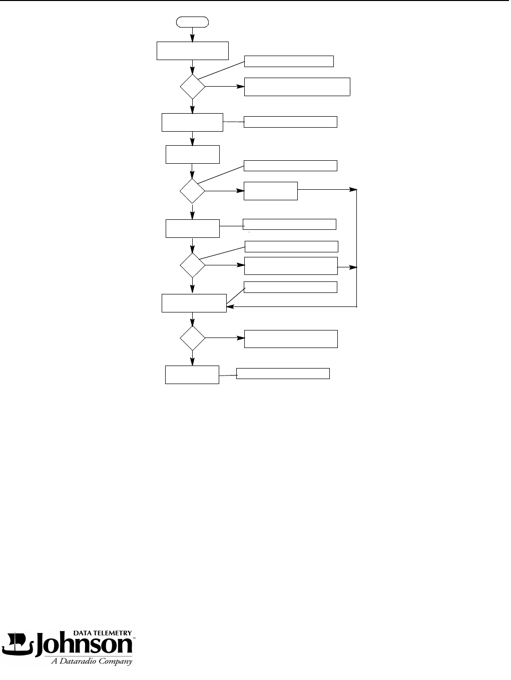
To isolate a receiver problem to a specific section, refer to the troubleshooting flowchart in Figure 5-1. Tests
referenced in the flowchart are described in the following information.
NOTE: Supply voltages are provided by the user.
5.3.1 SUPPLY VOLTAGES AND CURRENT
Measure the supply voltages on the following pins at interface connector J201:
Pin 4 - 5.0V DC Receive
Pin 5 - 5.0V DC
Place a DC ammeter in the supply line to the transceiver and the following maximum currents should be
measured:
Pin 4 - 400 µA
Pin 5 - 400 µA
5.3.2 MIXER/DETECTOR (U201)
Data Output
Using a .01 µF coupling capacitor, inject a 21.45 MHz, 1 mV signal, modulated with 1 kHz at ±3 kHz
deviation at U241, pin 1. The signal output at U241, pin 8 should be approximately 150 mV P-P.
NOTE: This signal consists of the 1 kHz modulation and harmonics of 450 kHz.
RSSI Output
The RSSI output on J201, pin 12 should be <900 mV DC with no signal applied, and >1.8V DC with a 1 mV
input signal.
SERVICING
5-4
Part No. 001-3422-003
Figure 5-1 RECEIVER SERVICING
5.3.3 SECOND LO (Q401)
Verify that the Second LO signal is present at U241, pin 4. The Second LO should be at 21.90 MHz and not
less than 500 mV P-P.
5.3.4 AUDIO BUFFER AMP (U241)
The Data output on J201, pin 13 should be 100-200 mV RMS, with the preceding injection signal. If these
levels are not correct, verify proper adjustment of L253 (see Section 6.7). The gain of U241 is 2.8 for 30 kHz
radios and 5.5 for 15 kHz radios.
5.3.5 CRYSTAL FILTERS
The 21.45 MHz IF signal is provided to the crystal filters Z221/Z222.
START
MEASURE CURRENT
OK
?
OK
?
NO
YES
YES
NO
REFER TO SECTION 5.3.2
CHECK FUSES AND
WIRE HARNESS CONNECTIONS
REFER TO SECTION 5.3
AND VOLTAGES
CHECK DATA
OUTPUT
REFER TO SECTION 5.3.2
CHECK
CHECK AUDIO
OK
?
YES
NO
OK
?
YES
NO
CHECK MIXER/
DETECT CIRCUIT
U241
CIRCUIT REFER TO SECTION 5.3.4
REFER TO SECTION 5.3.3
REPLACE DEFECTIVE
COMPONENT
REFER TO SECTION 5.3.5
CHECK BUFFERS
CRYSTAL FILTERS
REPAIR DEFECTIVE
STAGE
CHECK RF AMP
FIRST MIXER REFER TO SECTION 5.3.6

SERVICING
5-5
Part No. 001-3422-003
5.3.6 MIXER (Q232)
The mixer converts the RF signal (132-174 MHz) to 21.45 MHz. The Local Oscillator is provided by the
VCO and Q302. The level of the LO should be approximately +3 dBm.
5.3.7 LNA (Q202)
The LNA provides approximately 16 dB of gain at 132-174 MHz. Q201 provides active bias to Q202.
5.3.8 PRESCALER FILTERS
The 2-pole and 3-pole LC prescaler filters limit the out-of-band signals from reaching the receiver. The 2-
pole filter has approximately 2.5 dB of loss and is composed of L201-L203, CR281/CR282, and C202-C207. The
3-pole filter has approximately 5.5 dB of loss and is composed of L212-L214, CR283/CR284, C214-C217 and
C221-C223. These filters are varactor tuned and require a control voltage to tune throughout the band. The
voltage on TP281 varies from 2.5V at the low end of the band to over 7V at the high end of the band.
5.3.9 ANTENNA SWITCH
CR561, CR562, L561, C561 and C563 form a Pi-network antenna switch. CR561 and CR562 are reversed
biased in Receive Mode.
5.4 TRANSMITTER SERVICING
5.4.1 SUPPLY VOLTAGES AND CURRENT
Measure the supply voltages on the following pins of interface connector J201:
Pin 2 - 13.3V DC nominal
Pin 3 - 3-16V DC
Pin 4 - 0.0V DC (while transmitting)
Pin 5 - 3-16V DC
Pin 6 - 2.5V DC ±1%/1.5V P-P max
Place a DC ammeter in the supply line to the transceiver and the following maximum currents should be
measured:
Pin 2 - 2.5A maximum
Pin 3 - 400 µA
Pin 5 - 400 µA

SERVICING
5-6
Part No. 001-3422-003
5.4.2 VCO
1. Check VCO after power splitter R894 for power output. (Power output should be at least -3 dBm.)
2. Check 9V Transmit (Q124, emitter).
3. If 9V is not present check Q124, U111, Q121, Q122, Q123, Q101 and Q102 (see Section 4.4.5).
4. Check voltages on Buffer Q501.
Input = 1.5V DC
Output = 3.5V DC
Power output should be at least 2 mW (+3 dBm) at C504 (50 ohm point).
5.4.3 PRE-DRIVER (Q511)
Check voltages on Q511.
Collector = 8.6V DC
Base = 2.2V DC
Emitter = 1.6V DC w/o RF (2.2V DC with RF)
Power output should be at least 100 mW (+13 dBm) at the junction of C517/L518 (50 ohm point).
5.4.4 FINAL AMPLIFIER (U531)
Check the voltages on U531.
Pin 2 = 5.5V DC (varies with power setting)
Pin 3 = 5.0V DC
Pin 4 = 12.7V DC
Power output at C551 should be 7.5-8.0W (+38.7 to +39 dBm).
5.4.5 ANTENNA SWITCH (CR561/CR562)
Check the antenna switch voltages.
CR561 = 8.6V DC
CR562 = 8.0V DC
The loss through the Antenna Switch should be 1.9 to 2.1 dB.
SERVICING
5-7
Part No. 001-3422-003
5.4.6 MODULATION INPUT (J201, PIN 6)
Check for audio/data signals at J201, pin 6, Y801, pin 1 and R821, pin 3.
5.4.7 TCXO (Y801)
1. Check Y801, pin 1 for 2.5V DC ±1%.
2. Adjust Y801 to set the transmitter to the frequency of operation.
3. If the frequency cannot be set to the frequency of operation, replace the TCXO.
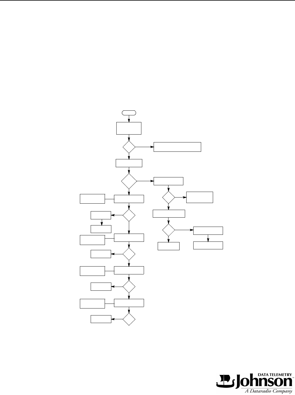
Figure 5-2 TRANSMITTER SERVICING
START
MEASURE
CURRENT AND
OK
?
NO
YES
MEASURE RF
WATTS
?
CHECK DEVIATION
TRANSMITTER
OK
OK
?
OK
?
NO
NO
NO
YES
YES
YES
WIRE HARNESS CONNECTIONS
CHECK FUSES AND
CHECK AUDIO
CHECK TCXO
ADJUST OR
CHANGE TCXO
OFF FREQ
5
VOLTAGES
OUTPUT POWER
(SECTION 5.4.6)
CIRCUITS
CHECK FREQUENCY
(SECTION 5.4.7)
Y801
OK
?
NO
YES
CHECK Q501
REFER TO
CHECK PRE-DRIVER
OK
?
NO
YES
CHECK A801
REFER TO
SECTION 5.4.2
CHECK DRIVER
SECTION 5.4.3
CHECK Q511
OK
?
NO
YES
REFER TO CHECK
POWER MODULE
SECTION 5.4.4
CHECK U521
OK
?
NO
REFER TO CHECK
ANTENNA SWITCH
SECTION 5.4.5
CHECK
CR561/562

SERVICING
5-8
Part No. 001-3422-003
This page intentionally left blank.

SECTION 6
6-1
Part No. 001-3422-003
ALIGNMENT PROCEDURE
6.1 GENERAL
Receiver or transmitter alignment may be necessary if repairs are made that could affect tuning. Alignment
points diagrams are located in Figure 6-3 or component layouts are located in Section 8.
Fabricated test cables should include power and ground, a transmit keying switch that shorts the keying line
to ground, data input and data output. The test setup must apply the various supply voltages and load the synthe-
sizer with channel information.
6.2 TEST EQUIPMENT
lModulation Analyzer, HP8901 or equivalent
lRF Signal Generator, HP8656 or equivalent
lPower Meter
lOscilloscope
lDigital Multimeter
lPower Supply, HP8264A or equivalent
lAudio Analyzer, HP8903A or equivalent
lMisc. cables, connectors, attenuators.
6.3 INITIAL SETTINGS
1. Adjust power supply voltage to +13.3V DC.
2. Turn off the power supply.
3. Connect RF and power cables.
4. Turn on the power supply.
5. Apply a 2.5V DC ±0.01V level to J201, pin 6.
6. Using a DC voltmeter, monitor the DC voltage at the junction of R826/R827 (wiper of R827), refer to Figure
6-3.
7. Adjust R827 to 1.50V DC ±0.05V.
8. Monitor the DC voltage at TP801 (see Figure 6-3 for top side access to TP801).
9. Adjust R805 for 2.5V DC ±0.025V.
10.Adjust R535 fully counterclockwise.

ALIGNMENT PROCEDURE
6-2
Part No. 001-3422-003
6.4 VCO CONTROL VOLTAGE
1. Connect the test setup shown in Figure 6-1.
2. Adjust R535 fully counterclockwise.
3. Load the synthesizer with the HIGHEST channel frequency in the band.
4. Key the transmitter.
5. Adjust C873 for 4.8V DC at TP831.
6. Unkey the transmitter.
7. The voltage at TP831 should be less than 4.9V.
8. Load the synthesizer with the LOWEST channel frequency in the band.
9. Key the transmitter.
10.The voltage at TP831 should be greater than .045V DC.
11.Unkey the transmitter.
12.The voltage at TP831 should be greater than 0.45V.
6.5 TRANSMITTER AND FREQUENCY
NOTE: If the radio is intended to use Diagnostics or is a Radio/Loader board combination go to Section 6.6.
1. Connect the test setup shown in Figure 6-1.
2. Load the synthesizer with a channel frequency in the MIDDLE of the band.
3. Key the transmitter.
4. The voltage at J201, pin 2 should be 13.3V DC.
(Do not transmit for extended periods.)
5. Adjust R535 clockwise for 5.0W +0.5/-0.2W. Adjust voltage and power if necessary.
6. Check the power at a channel frequency on the LOW and HIGH ends of the band. The power output should be
5W ±1W with current less than 2.5A .

ALIGNMENT PROCEDURE
6-3
Part No. 001-3422-003
6.5.1 MODULATION ALIGNMENT
1. Apply a 1V p-p, 100 Hz, +2.5V DC bias, square-wave to J201, pin 6.
2. Transmit into the modulation analyzer and observe modulation output on the oscilloscope. Set the modulation
analyzer high pass filtering OFF and no less than a 15 kHz low pass filter.
3. Preset R827 to 1.5 VDC on the wiper.
4. Load the synthesizer with a channel frequency at the MIDDLE of the band.
5. Adjust R825 for a flat square wave.
6. Apply a 100 Hz, +2.5V DC biased, sine-wave to J201, pin 6. The modulation analyzer should still have the 15
kHz lowpass filter selected.
7. Adjust the audio analyzer output level to achieve a transmit deviation of:
1.5 kHz for 15 kHz BW radios
3.0 kHz for 30 kHz BW radios
8. Load the synthesizer with a channel frequency at the LOW end of the band.
9. Input a 100 Hz, +2.5V DC biased, sine-wave and set a 0 dB reference on the Modulation Analyzer.
10.Apply a 1 kHz, +2.5V DC biased, sine-wave. The level should be within ±3.5 dB of the reference at 100 Hz.
11.Load the synthesizer with a channel frequency in the MIDDLE of the band.
12.Input a 100 Hz, +2.5V DC biased, sine-wave and set a 0 dB reference on the Modulation Analyzer.
13.Apply a 1 kHz, +2.5V DC biased, sine-wave. The level should be within ±0.5 dB of the reference at 100 Hz.
14.Load the synthesizer with a channel frequency in the HIGH end of the band.
15.Input a 100 Hz, +2.5V DC biased, sine-wave and set a 0 dB reference on the Modulation Analyzer.
16.Apply a 1 kHz, +2.5V DC biased, sine-wave. The level should be within ±3.5 dB of the reference at 100 Hz.
17.Unkey the transmitter.
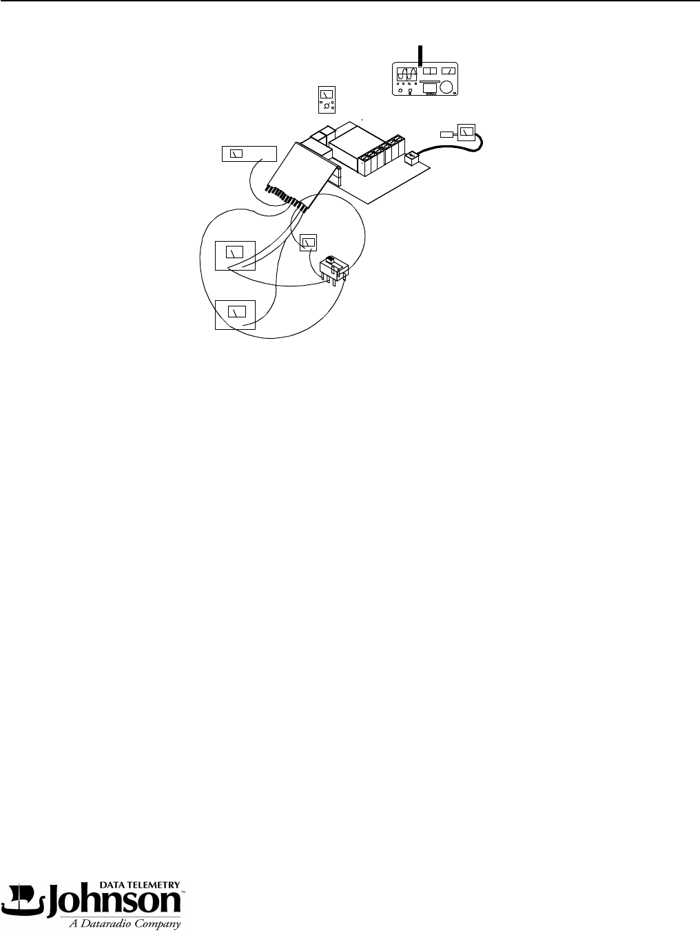
ALIGNMENT PROCEDURE
6-4
Part No. 001-3422-003
Figure 6-1 TRANSMITTER TEST SETUP
6.6 TRANSMITTER/FREQUENCY WITH LOADER
NOTE: If the radio is not intended to use Diagnostics go to Section 6.5.
NOTE: Subtract the current drawn by the Test Loader or any Interface Units from all measurements.
1. Set the Diagnostic Enable DAC (DAC4) to 255, (FFh).
2. Select a Transmit channel frequency in the MIDDLE of the band. Make sure voltage at J201, pin 2 is 13.3V DC.
3. Adjust R535 fully clockwise for maximum power output.
4. Adjust the Power Adjust DAC setting (DAC1) to set the power output to 5W ±0.3W. Make sure voltage at J201,
pin 2 is 13.3V DC.
5. Adjust voltage and power if necessary.
6. Repeat Step 5 for channels on the LOW and HIGH ends of the band.
7. Power output should be 4.7-5.3W (50% duty cycle) and current should be less than 2.5A.
8. Select a Transmit channel frequency in the MIDDLE of the band
POWER SUPPLY
+7.5V DC
POWER SUPPLY
+5V DC
+-
TX
RX
VOLTMETER
DC
+
-
WATTMETER5W, 50 OHM
DUMMY LOAD
COMMUNICATIONS
SERVICE MONITOR
0-1.5A
DC AMMETER
+-
ANALYZER
MODULATION

ALIGNMENT PROCEDURE
6-5
Part No. 001-3422-003
9. Adjust the frequency displayed on the Modulation Analyzer to the desired channel frequency by adjusting the
TCXO (Y801).
6.6.1 MODULATION ADJUSTMENT
1. Apply a 1V p-p, 100 Hz, 2.5V DC bias, square wave to J201, pin 6.
2. Transmit into the modulation analyzer and observe modulation output on the oscilloscope. The modulation
analyzer should not have any high pass filtering selected and no less than a 15 kHz low pass filter.
3. Select a Transmit channel frequency in the MIDDLE of the band. The DAC value should be "125" (the voltage
at the wiper of R827 should be set to 1.5V DC).
4. If the square wave is rolled off on the edges, adjust R825 up in value for the flattest square wave.
5. If the square wave is peaked on the edges, adjust R825 down in value for the flattest square wave.
6. Adjust the Modulation Adjust DAC (DAC2) for the flattest square wave.
7. Repeat Step 6 for channels on the LOW and HIGH ends of the band.
8. Input a 100 Hz, 2.5V DC bias, sinewave to J201, pin 6. The modulation analyzer should still have the 15 kHz
low pass filter selected.
9. Adjust the audio analyzer output level to achieve a transmit deviation of:
1.5 kHz for 15 kHz radios or 3 kHz for 30 kHz radios.
10.Select a Transmit channel frequency at the LOW end of the band.
11.Input a 100 Hz, +2.5V DC biased, sine-wave and set a 0 dB reference on the Modulation Analyzer.
12.Apply a 1 kHz, +2.5V DC biased, sine-wave. The level should be within ±0.5 dB of the reference at 100 Hz.
13.Select a Transmit channel frequency in the MIDDLE of the band.
14.Input a 100 Hz, +2.5V DC biased, sine-wave and set a 0 dB reference on the Modulation Analyzer.
15.Apply a 1 kHz, +2.5V DC biased, sine-wave. The level should be within ±0.5 dB of the reference at 100 Hz.
16. Select a Transmit channel frequency in the HIGH end of the band.
17.Input a 100 Hz, +2.5V DC biased, sine-wave and set a 0 dB reference on the Modulation Analyzer.
18.Apply a 1 kHz, +2.5V DC biased, sine-wave. The level should be within ±0.5 dB of the reference at 100 Hz.
19.Unkey the transmitter.

ALIGNMENT PROCEDURE
6-6
Part No. 001-3422-003
6.7 RECEIVER
C A U T I O N
Do not key the transmitter with the generator connected because severe generator damage may result.
NOTE: If the radio is intended to use Diagnostics or is a Radio/Loader board combination go to Section 6.8.
NOTE: All distortion and SINAD measurements are performed with psophometric audio filtering.
1. Connect the test setup shown in Figure 6-2.
2. Preset tuning slugs of L201, L203, L212, L221 and L224 flush with the top of the can.
3. Preset tuning slugs of L231 and L242 full clockwise and re-adjust L242 counter-clockwise 2 full turns.
4. Preset C241 to the center position (slot in-line with axis of the part).
5. Load the synthesizer with a receive channel frequency at the LOW end of the band (-21.45 MHz).
6. Apply a -47 dBm signal from the RF signal genertor to J501 on the radio. Adjust deviation for 1.5 kHz with
1.0 kHz tone for 15 kHz radios and 3 kHz deviation with 1.0 kHz tone for 30 kHz radios.
NOTE: Maintain these deviation levels throughout the test when measuring AC levels, SINAD and %
distortion.
7. Adjust R920 for 2.5V DC ±0.05V at TP281.
8. Adjust L251 for 2.5V ±0.05V at TP251.
9. Preset L253 for 2.5V DC ±0.05V at J201, pin 13.
10.Lower the RF generator 1.5 kHz for 15.0 kHz radios and 3.0 kHz for 30 kHz radios. Adjust C241 for minimum
audio distortion.
11.Reset the generator back to center frequency. Tune L231 counter-clockwise for minimum distortion. Again tune
L242 for minimum distortion.
12.Readjust L253 for minimum distortion (use 30 kHz LPF only)
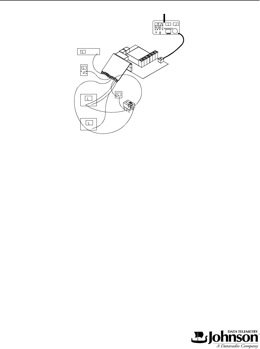
ALIGNMENT PROCEDURE
6-7
Part No. 001-3422-003
.
Figure 6-2 RECEIVER TEST SETUP
13.Verify that the receive audio RMS voltage is 150 mV ±50 mV.
14.Measure the % distortion (spec is <3% psophometrically weighted).
15.Adjust the amplitude of the RF signal generator on J501 until an 18 dB SINAD level (psophometrically
weighted) is reached.
16.Adjust L221, L212, L224, L201 and L203 in turn for the best SINAD reading adjusting the generator output as
necessary to maintain an 18 dB SINAD level. DO NOT turn the slug more than 2-turns from the top of the coil.
17.Turn the slug of L221 1/2-turn clockwise. This helps to center the filter tracking across the band.
18.Measure the 12 dB SINAD sensitivity. The RF input level should be less than -116 dBm (0.35 µV).
19.Load the synthesizer with a receive channel frequency to the MIDDLE of the band.
20.Set the signal generator to the same frequency with an amplitude of -116 dBm.
21.Adjust R920 for the best SINAD reading.
22.Adjust the RF input level until 12 dB SINAD is measured. The RF input level should be less than
-116 dBm (0.35 µV).
POWER SUPPLY
+7.5V DC
POWER SUPPLY
+5V DC
+-
TX
RX
VOLTMETER
DC
+
-
COMMUNICATIONS
SERVICE MONITOR
0-1.5A
DC AMMETER
+-
ANALYZER
MODULATION

ALIGNMENT PROCEDURE
6-8
Part No. 001-3422-003
23.Adjust generator RF level to -120 dBm and measure DC (RSSI) voltage on J201, pin 12 of the radio
(spec is less than or equal to 0.90V DC).
24.Adjust generator RF level to -60 dBm and measure DC (RSSI) voltage on J201, pin 12 of the radio
(spec is greater than or equal to 1.75V DC).
6.8 RECEIVER WITH LOADER BOARD
C A U T I O N
Do not key the transmitter with the generator connected because severe generator damage may result.
NOTE: If the radio is NOT intended to use Diagnostics or is NOT a Radio/Loader board combination see
Section 6.7.
NOTE: All distortion and SINAD measurements are performed with psophometric audio filtering.
1. Set the Diagnostic Enable DAC (DAC 4) to 255, (FFh).
2. Preset tuning slugs of L201, L203, L212, L221 and L224 flush with the top of the can.
3. Preset tuning slugs of L231 and L242 full clockwise and re-adjust L242 counter-clockwise 2 full turns.
4. Preset C241 to the center position (slot in-line with axis of the part).
5. Select a receive channel frequency at the LOW end of the band (-21.45 MHz).
6. Apply a -47 dBm signal from the RF signal generator to J501 on the radio. Adjust deviation for:
1.5 kHz with 1.0 kHz tone for 15 kHz radios or 3 kHz deviation with 1.0 kHz tone for 30 kHz radios.
NOTE: Maintain these deviation levels throughout the test when measuring AC levels, SINAD and % distortion.
7. Adjust the Front End DAC (DAC 3) value to set the voltage on TP281 to 2.5V DC ±0.05V. The DAC setting
will be about 74.
8. Adjust L251 for 2.5V ±0.05V at TP251.
9. Preset L253 for 2.5V DC ±0.05V at J201, pin 13.
10.Lower the RF generator 1.5 kHz for 15.0 kHz radios and 3.0 for 30 kHz radios. Adjust C241 for minimum audio
distortion
11.Reset generator back to center frequency. Tune L231 counter-clockwise for minimum distortion. Again tune
L242 for minimum distortion.

ALIGNMENT PROCEDURE
6-9
Part No. 001-3422-003
12.Readjust L253 for minimum distortion (use 30 kHz LPF only).
13.Verify that the receive audio RMS voltage is 150 mV ±50 mV.
14.Measure the % distortion (spec is <3% psophometrically weighted).
15.Adjust the amplitude of the RF signal generator on J501 until an 18 dB SINAD level (psophometrically
weighted) is reached.
16.Adjust L221, L212, L224, L201 and L203 in turn for the best SINAD reading adjusting the generator output as
necessary to maintain an 18 dB SINAD level. DO NOT turn the slug more than 2-turns from the top of the coil.
17.Turn the slug of L221 1/2-turn clockwise. This helps to center the filter tracking across the band.
18.Measure the 12 dB SINAD sensitivity. The RF input level should be less than -116 dBm (0.35 µV).
19.Select a receive channel frequency to the MIDDLE of the band.
20.Set the signal generator to the same frequency with an amplitude of -116 dBm.
21.Adjust the Front-End DAC (DAC 3) value to peak the SINAD reading (this is a very gradual peak).
22.Adjust the RF input level until 12 dB SINAD is measured. The RF input level should be less than -116 dBm
(0.35 µV).
23.Adjust generator RF level to -120 dBm and measure DC (RSSI) voltage on J201, pin 12 of the radio
(spec is less than or equal to 0.90V DC).
24.Adjust generator RF level to -60 dBm and measure DC (RSSI) voltage on J201, pin 12 of the radio
(spec is greater than or equal to 1.75V DC).
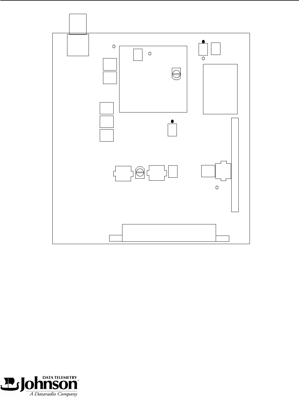
ALIGNMENT PROCEDURE
6-10
Part No. 001-3422-003
Figure 6-3 ALIGNMENT POINTS DIAGRAM
J501
VCO
TP831
R827
R805
Y801
J201
6 1
14 13
L253
R535
L242
C241
TP281
TP801
R825
C873
R823
L231
TP251
L251
L201
L203
L212
L221
L224

SECTION 7
7-1
Part No. 001-3422-003
PARTS LIST
3422 TRANSCEIVER
PART NO. 242-3422-XXX
SYMBOL NUMBER DESCRIPTION PART NUMBER
A 531 Directional coupler 692-5033-001
C 101 .001 µF ±10% X7R 0603 610-3675-102
C 102 1 µµF 16V SMD tantalum 610-2625-109
C 103 .001 µµF ±±10% X7R 0603 610-3675-102
C 104 .01 µµF ±±10% X7R 0603 610-3675-103
C 105 1 µµF 16V SMD tantalum 610-2625-109
C 106 .001 µµF ±±10% X7R 0603 610-3675-102
C 111 .01 µµF ±±10% X7R 0603 610-3675-103
C 112 .001 µµF ±±10% X7R 0603 610-3675-102
C 113 .001 µµF ±±10% X7R 0603 610-3675-102
C 114 .1 µµF ±±10% X7R 0603 610-3675-104
C 115 .01 µµF ±±10% X7R 0603 610-3675-103
C 116 .0082 µF ±10% X7R 0805 610-3605-822
C 121 .001 µµF ±±10% X7R 0603 610-3675-102
C 122 .001 µµF ±±10% X7R 0603 610-3675-102
C 123 .01 µµF ±±10% X7R 0603 610-3675-103
C 124 .001 µµF ±±10% X7R 0603 610-3675-102
C 125 1 µµF 16V SMD tantalum 610-2625-109
C 131 .001 µµF ±±10% X7R 0603 610-3675-102
C 132 1 µµF 16V SMD tantalum 610-2625-109
C 133 .001 µµF ±±10% X7R 0603 610-3675-102
C 134 .01 µµF ±±10% X7R 0603 610-3675-103
C 135 1 µµF 16V SMD tantalum 610-2625-109
C 136 .001 µµF ±±10% X7R 0603 610-3675-102
C 137 .01 µµF ±±10% X7R 0603 610-3675-103
C 141 1 µµF 16V SMD tantalum 610-2625-109
C 142 .001 µµF ±±10% X7R 0603 610-3675-102
C 143 .01 µµF ±±10% X7R 0603 610-3675-103
C 144 .01 µµF ±±10% X7R 0603 610-3675-103
C 145 1 µµF 16V SMD tantalum 610-2625-109
C 146 .001 µµF ±±10% X7R 0603 610-3675-102
C 151 .001 µµF ±±10% X7R 0603 610-3675-102
C 152 .001 µµF ±±10% X7R 0603 610-3675-102
C 153 .001 µµF ±±10% X7R 0603 610-3675-102
C 154 .001 µµF ±±10% X7R 0603 610-3675-102
C 155 .001 µµF ±±10% X7R 0603 610-3675-102
C 156 .001 µµF ±±10% X7R 0603 610-3675-102
C 157 100 pF ±±5% NPO 0603 610-3674-101
C 158 100 pF ±±5% NPO 0603 610-3674-101
C 159 100 pF ±±5% NPO 0603 610-3674-101

PARTS LIST
7-2
Part No. 001-3422-003
SYMBOL NUMBER DESCRIPTION PART NUMBER
C 160 100 pF ±5% NPO 0603 610-3674-101
C 161 .001 µµF ±±10% X7R 0603 610-3675-102
C 162 .001 µµF ±±10% X7R 0603 610-3675-102
C 163 .001 µµF ±±10% X7R 0603 610-3675-102
C 171 1 µµF 16V SMD tantalum 610-2625-109
C 172 .001 µµF ±±10% X7R 0603 610-3675-102
C 201 .001 µµF ±±10% X7R 0603 610-3675-102
C 202 15 pF ±±5% NPO 0603 610-3674-150
C 203 22 pF ±±5% NPO 0603 610-3674-220
C 204 4.7 pF ±±.1% NPO 0603 610-3673-479
C 205 4.7 pF ±±.1% NPO 0603 610-3673-479
C 206 15 pF ±±5% NPO 0603 610-3674-150
C 207 22 pF ±±5% NPO 0603 610-3674-220
C 208 .001 µµF ±±10% X7R 0603 610-3675-102
C 209 .001 µµF ±±10% X7R 0603 610-3675-102
C 211 .001 µµF ±±10% X7R 0603 610-3675-102
C 212 .001 µµF ±±10% X7R 0603 610-3675-102
C 213 27 pF ±±5% NPO 0603 610-3674-270
C 214 15 pF ±±5% NPO 0603 610-3674-150
C 215 27 pF ±±5% NPO 0603 610-3674-270
C 216 4.7 pF ±±.1% NPO 0603 610-3673-479
C 217 15 pF ±±5% NPO 0603 610-3674-150
C 218 .001 µµF ±±10% X7R 0603 610-3675-102
C 211 4.7 pF ±±.1% NPO 0603 610-3673-479
C 222 15 pF ±±5% NPO 0603 610-3674-150
C 223 27 pF ±±5% NPO 0603 610-3674-270
C 230 1.8 pF ±±.1% NPO 0603 610-3673-189
C 232 .001 µµF ±±10% X7R 0603 610-3675-102
C 233 .01 µµF ±±10% X7R 0603 610-3675-103
C 234 56 pF ±±5% NPO 0603 610-3674-560
C 235 .01 µµF ±±10% X7R 0603 610-3675-103
C 237 .01 µµF ±±10% X7R 0603 610-3675-103
C 241 1.5-5 pF SMD ceramic 612-1602-001
C 242 8.2 pF NPO J 0805 610-3601-829
C 243 3.9 pF NPO J 0805 610-3601-399
C 244 47 pF ±±5% NPO 0603 610-3674-470
C 245 .01µµF X7R K 0805 610-3605-103
C 246 .01 µµF ±±10% X7R 0603 610-3675-103
C 250 .01 µµF ±±10% X7R 0603 610-3675-103
C 251 .01 µµF ±±10% X7R 0603 610-3675-103
C 252 .01 µµF ±±10% X7R 0603 610-3675-103
C 253 330 pF ±±5% NPO 0603 610-3674-331
C 254 100 pF ±±5% NPO 0603 610-3674-101
C 255 .001 µµF ±±10% X7R 0603 610-3675-102
C 256 100 pF ±±5% NPO 0603 610-3674-101
C 257 100 pF ±±5% NPO 0603 610-3674-101

PARTS LIST
7-3
Part No. 001-3422-003
SYMBOL NUMBER DESCRIPTION PARTNUMBER
C 259 220 pF ±±5% NPO 0603 610-3674-221
C 260 .010 µF ±10% X7R 0603 610-3609-103
C 264 47 µF 10V SMD tantalum 610-2624-470
C 265 .01 µµF ±±10% X7R 0603 610-3675-103
C 266 .001 µµF ±±10% X7R 0603 610-3675-102
C 267 .01 µµF ±±10% X7R 0603 610-3675-103
C 268 .01 µµF ±±10% X7R 0603 610-3675-103
C 271 .01 µµF ±±10% X7R 0603 610-3675-103
C 272 .01 µµF ±±10% X7R 0603 610-3675-103
C 273 .01 µµF ±±10% X7R 0603 610-3675-103
C 275 .01 µµF ±±10% X7R 0603 610-3675-103
C 276 .01 µµF ±±10% X7R 0603 610-3675-103
C 277 10 pF ±±.1% NPO 0603 610-3673-100
C 278 .01 µµF ±±10% X7R 0603 610-3675-103
C 279 .01 µµF ±±10% X7R 0603 610-3675-103
C 281 .001 µµF ±±10% X7R 0603 610-3675-102
C 282 .001 µµF ±±10% X7R 0603 610-3675-102
C 283 .001 µµF ±±10% X7R 0603 610-3675-102
C 284 .001 µµF ±±10% X7R 0603 610-3675-102
C 285 .001 µµF ±±10% X7R 0603 610-3675-102
C 301 .001 µµF ±±10% X7R 0603 610-3675-102
C 302 .01 µµF ±±10% X7R 0603 610-3675-103
C 303 .001 µµF ±±10% X7R 0603 610-3675-102
C 304 12 pF ±5% ±5% NPO 0603 610-3674-120
C 305 22 pF 5% NPO 0603 610-3674-220
C 306 .001 µµF ±±10% X7R 0603 610-3675-102
C 307 7.5 pF ±±1% NPO 0603 610-3673-759
C 501 .001 µµF ±±10% X7R 0603 610-3675-102
C 502 .001 µµF ±±10% X7R 0603 610-3675-102
C 503 .001 µµF ±±10% X7R 0603 610-3675-102
C 504 .001 µµF ±±10% X7R 0603 610-3675-102
C 505 22 pF ±±5% NPO 0603 610-3674-220
C 506 68 pF ±±5% NPO 0603 610-3674-680
C 507 .01 µµF ±±10% X7R 0603 610-3675-103
C 508 .001 µµF ±±10% X7R 0603 610-3675-102
C 511 .001 µµF ±±10% X7R 0603 610-3675-102
C 512 12 pF ±±5% NPO 0603 610-3674-120
C 513 .01 µµF ±±10% X7R 0603 610-3675-103
C 514 .001 µµF ±±10% X7R 0603 610-3675-102
C 515 .01 µµF ±±10% X7R 0603 610-3675-103
C 516 .001 µµF ±±10% X7R 0603 610-3675-102

PARTS LIST
7-4
Part No. 001-3422-003
SYMBOL NUMBER DESCRIPTION PART NUMBER
C 517 .001 µµF ±±10% X7R 0603 610-3675-102
C 518 6.8 pF ±±.1% NPO 0603 610-3673-689
C 519 .001 µµF ±±10% X7R 0603 610-3675-102
C 521 .001 µµF ±±10% X7R 0603 610-3675-102
C 522 1 µµF 16V SMD tantalum 610-2625-109
C 523 .01 µµF ±±10% X7R 0603 610-3675-103
C 524 .001 µµF ±±10% X7R 0603 610-3675-102
C 531 .001 µF ±10% X7R 0603 610-3675-102
C 532 .001 µµF ±±10% X7R 0603 610-3675-102
C 533 .001 µµF ±±10% X7R 0603 610-3675-102
C 534 .001 µµF ±±10% X7R 0603 610-3675-102
C 535 .001 µµF ±±10% X7R 0603 610-3675-102
C 536 .01 µµF ±±10% X7R 0603 610-3675-103
C 541 22 pF±±5% NPO 0603 610-3674-220
C 542 68 pF ±±5% NPO 0603 610-3674-680
C 543 .01 µµF ±±10% X7R 0603 610-3675-103
C 544 .001 µµF ±±10% X7R 0603 610-3675-102
C 544 .001 µµF ±±10% X7R 0603 610-3675-102
C 545 .001 µµF ±±10% X7R 0603 610-3675-102
C 551 .001 µµF ±±10% X7R 0603 610-3675-102
C 552 22 ±±5% NPO 0805 610-3601-220
C 553 47 pF ±±5% NPO 0805 610-3601-470
C 554 51 pF ±±5% NPO 0805 610-3601-510
C 555 47 pF ±±5% NPO 0805 610-3601-470
C 556 27 pF ±±5% NPO 0805 610-3601-270
C 557 .001 µµF ±±10% X7R 0603 610-3675-102
C 561 10 pF ±±5% NPO 0805 610-3601-100
C 562 .001 µµF ±±10% X7R 0603 610-3675-102
C 563 15 pF ±±5% NPO 0603 610-3674-150
C 564 .001 µµF ±±10% X7R 0603 610-3675-102
C 581 .001 µµF ±±10% X7R 0603 610-3675-102
C 591 .001 µµF ±±10% X7R 0603 610-3675-102
C 592 .01 µµF ±±10% X7R 0603 610-3675-103
C 593 .001 µµF ±±10% X7R 0603 610-3675-102
C 594 .01 µµF ±±10% X7R 0603 610-3675-103
C 801 .01 µµF ±±10% X7R 0603 610-3675-103
C 802 .001 µµF ±±10% X7R 0603 610-3675-102
C 803 .01 µµF ±±10% X7R 0603 610-3675-103
C 804 .01 µµF ±±10% X7R 0603 610-3675-103
C 805 .001 µµF ±±10% X7R 0603 610-3675-102
C 806 .01 µµF ±±10% X7R 0603 610-3675-103
C 807 2.2 pF ±±.1% NPO 0603 610-3673-229
C 808 220 pF ±±5% NPO 0603 610-3674-221
C 809 220 pF ±±5% NPO 0603 610-3674-221
C 810 120 pF ±±5% NPO 0603 610-3674-121
C 811 .01 µµF ±±10% X7R 0603 610-3675-103
C 812 .01 µµF ±±10% X7R 0603 610-3675-103

PARTS LIST
7-5
Part No. 001-3422-003
C 813 .001 µµF ±±10% X7R 0603 610-3675-102
C 814 .01 µµF ±±10% X7R 0603 610-3675-103
C 815 .001 µµF ±±10% X7R 0603 610-3675-102
C 816 5.6 pF ±±0.1% NPO 0603 610-3673-569
C 817 1 pF ±±0.1% NPO 0603 610-3673-109
C 821 1 µµF 16V SMD tantalum 610-2625-109
C 822 .001 µµF ±±10% X7R 0603 610-3675-102
C 823 .01 µF ±5% X7R 1206 610-3609-103
C 824 .001 µµF ±±10% X7R 0603 610-3675-102
C 825 .001 µµF ±±10% X7R 0603 610-3675-102
C 826 1 µF 16V SMD tantalum 610-2625-109
C 831 100 pF ±±5% NPO 0603 610-3674-101
C 832 .033 µF ±10% X7R 1206 610-3606-333
C 833 .001 µµF ±10% X7R 0805 610-3605-102
C 836 .0047 µµF ±10% X7R 0805 610-3605-472
C 841 .01 µµF ±±10% X7R 0603 610-3675-103
C 842 .001 µµF ±±10% X7R 0603 610-3675-102
C 843 .01 µµF ±±10% X7R 0603 610-3675-103
C 844 .001 µµF ±±10% X7R 0603 610-3675-102
C 845 .01 µµF ±±10% X7R 0603 610-3675-103
C 846 .001 µµF ±±10% X7R 0603 610-3675-102
C 847 .01 µµF ±±10% X7R 0603 610-3675-103
C 848 .001 µµF ±±10% X7R 0603 610-3675-102
C 849 .01 µµF ±±10% X7R 0603 610-3675-103
C 850 .001 µµF ±±10% X7R 0603 610-3675-102
C 851 .001 µµF ±±10% X7R 0603 610-3675-102
C 852 .001 µµF ±±10% X7R 0603 610-3675-102
C 853 6.8 pF ±±0.1% NPO 0603 610-3673-689
C 854 220 pF ±±5% NPO 0603 610-3674-221
C 855 3.9 pF ±0±0.1% NPO 0603 610-3673-399
C 856 3.9 pF ±0±0.1% NPO 0603 610-3673-399
C 858 .001 µµF ±±10% X7R 0603 610-3675-102
C 863 100 pF ±±5% NPO 0603 610-3674-101
C 865 100 pF ±±5% NPO 0603 610-3674-101
C 866 1 µµF 16V SMD tantalum 610-2625-109
C 871 .001 µµF ±±10% X7R 0603 610-3675-102
C 872 39 pF ±±5% NPO 0603 610-3674-390
C 873 2.5-10 pF ceramic SMD 612-1602-002
C 874 47 pF ±±5% NPO 0603 610-3674-470
C 875 68 pF ±±5% NPO 0603 610-3674-680
C 876 .001 µµF ±±10% X7R 0603 610-3675-102
C 877 18 pF ±±0.1% NPO 0603 610-3674-180
C 881 .001 µF ±10% X7R 0603 610-3675-102
C 882 .01 µµF ±±10% X7R 0603 610-3675-103
C 883 27 pF ±±5% NPO 0603 610-3674-270
C 884 22 pF ±±5% NPO 0603 610-3674-220
C 891 .001 µµF ±±10% X7R 0603 610-3675-102
SYMBOL NUMBER DESCRIPTION PART NUMBER

PARTS LIST
7-6
Part No. 001-3422-003
C 892 10 pF ±±0.1% NPO 0603 610-3673-100
C 893 .001 µµF ±±10% X7R 0603 610-3675-102
C 901 4.7 µµF 16V SMD tantalum 610-2625-479
C 902 .01 µµF ±±10% X7R 0603 610-3675-103
C 903 .001 µµF ±±10% X7R 0603 610-3675-102
C 911 .01 µµF ±±10% X7R 0603 610-3675-103
C 912 .01 µµF ±±10% X7R 0603 610-3675-103
C 913 .01 µµF ±±10% X7R 0603 610-3675-103
C 914 .01 µµF ±±10% X7R 0603 610-3675-103
C 915 .01 µµF ±±10% X7R 0603 610-3675-103
C 916 .01 µµF ±±10% X7R 0603 610-3675-103
C 917 1 µµF 10V SMD tantalum 610-2624-109
C 918 330 pF ±±5% NPO 0603 610-3674-331
C 920 .001 µµF ±±10% X7R 0603 610-3675-102
C 921 .01 µµF ±±10% X7R 0603 610-3675-103
CR201 Switching diode SOT-23 623-1504-002
CR251 Varactor BB535 SOD-323 623-5005-022
CR281 Dual varactor MMBV609 623-5005-023
CR282 Dual varactor MMBV609 623-5005-023
CR283 Dual varactor MMBV609 623-5005-023
CR284 Dual varactor MMBV609 623-5005-023
CR285 Dual varactor MMBV609 623-5005-023
CR561 Switch PIN diode SOT-23 623-1504-001
CR562 Switch PIN diode SOT-23 623-1504-001
CR591 Hot carrier diode SOT-23 623-1504-016
CR592 Hot carrier diode SOT-23 623-1504-016
CR851 Switch PIN diode SOT-23 623-1504-001
CR852 Dual varactor MMBV609 623-5005-023
CR853 Dual varactor MMBV609 623-5005-023
CR854 Dual varactor MMBV609 623-5005-023
CR855 Switch PIN diode SOT-23 623-1504-001
CR861 Varactor BB535 SOD-323 623-5005-022
CR862 Varactor BB535 SOD-323 623-5005-022
CR901 Varactor BB535 SOD-323 623-5005-022
CR902 Dual switch diode SOT-23 623-1504-023
EP111 Ferrite bead SMD 617-2503-001
EP200 Mini ceramic xtal pin insolator 010-0345-280
EP501 Ferrite bead SMD 617-2503-001
EP531 Ferrite bead SMD 617-2503-001
EP532 Ferrite bead SMD 617-2503-001
EP533 Ferrite bead SMD 617-2503-010
EP534 Ferrite bead SMD 617-2503-001
HW103 4-40 machine panhead ZPS 675-1604-010
HW104 Grafoil M577xx 018-1007-102
J 201 14-pos single row receptacle 615-7110-214
J 501 Jack right angle PC mount 142-0701-501
L 201 3.5T shielded 5 mm coil 642-1021-003
SYMBOL NUMBER DESCRIPTION PART NUMBER

PARTS LIST
7-7
Part No. 001-3422-003
L 202 180 nH ±10% SMD 0805 642-9003-188
L 203 3.5T shielded 5 mm coil 642-1021-003
L 204 15 nH ±10% SMD inductor 642-9003-157
L 211 82 nH ±5% SMD 0805 642-9003-827
L 212 3.5T shielded 5 mm coil 642-1021-003
L 213 270 nH ±10% SMD inductor 642-9003-278
L 214 330 nH ±10% SMD inductor 642-9003-338
L 221 3.5T shielded 5 mm coil 642-1021-003
L 222 270 nH ±10% SMD inductor 642-9003-278
L 223 330 nH ±10% SMD inductor 642-9003-338
L 224 3.5T shielded 5 mm coil 642-1021-003
L 231 1 µH ±6% variable inductor 642-1012-015
L 232 470 nH ±10% SMD inductor 642-9003-478
L 233 470 nH ±10% SMD inductor 642-9003-478
L 242 1 µH ±6% variable inductor 642-1012-015
L 251 1 µH ±6% variable inductor 642-1012-015
L 252 470 nH ±10% SMD inductor 642-9003-478
L 253 680 µH quad coil 642-5102-001
L 301 82 nH ±10% SMD inductor 642-9003-827
L 302 82 nH ±10% SMD inductor 642-9003-827
L 501 3.9 µH SMD inductor 642-9001-399
L 511 56 nH inductor LL2012 F56N 642-9003-567
L 512 1 µH inductor SMD 642-9001-109
L 513 68 nH ±10% SMD 0805 642-9003-687
L 551 43 nH 10-turn air core SMD 642-0030-010
L 552 43 nH 10-turn air core SMD 642-0030-010
L 553 43 nH 10-turn air core SMD 642-0030-010
L 554 43 nH 10-turn air core SMD 642-0030-010
L 555 3.9 µH SMD inductor 642-9001-399
L 561 43 nH 10-turn air core SMD 642-0030-010
L 801 470 nH ±10% SMD 0805 642-9003-478
L 802 470 nH ±10% SMD 0805 642-9003-478
L 803 470 nH ±10% SMD 0805 642-9003-478
L 804 470 nH ±10% SMD 0805 642-9003-478
L 811 120 nH ±10% SMD 0805 642-9003-128
L 812 470 nH ±10% SMD 0805 642-9003-478
L 851 1 µH SMD inductor 642-9001-109
L 852 1 µH SMD inductor 642-9001-109
L 853 1 µH SMD inductor 642-9001-109
L 854 1 µH SMD inductor 642-9001-109
L 855 1 µH SMD inductor 642-9001-109
L 871 82 nH ±10% SMD 0805 642-9003-827
L 872 12.5 nH 4T air core SMD 642-0030-004
L 873 470 nH ±10% SMD 0805 642-9003-478
L 881 82 nH ±10% SMD 0805 642-9003-827
L 891 82 nH ±10% SMD 0805 642-9003-827
MP101 Heat sink 014-0778-047
SYMBOL NUMBER DESCRIPTION PART NUMBER

PARTS LIST
7-8
Part No. 001-3422-003
SYMBOL NUMBER DESCRIPTION PART NUMBER
MP102 VHF/UHF module shield 017-2225-756
MP107 Low pass top shield 017-2225-771
MP108 Synthesizer bottom shield 017-2225-772
MP109 Driver bottom shield 017-2225-773
MP110 Low pass bottom shield 017-2225-774
MP801 VCO can 017-2225-751
PC001 PC board 035-3422-050
Q 101 NPN digital transistor 676-0013-046
Q 102 PNP digital transistor 676-0013-032
Q 121 NPN digital transistor 676-0013-046
Q 122 NPN digital transistor 676-0013-046
Q 123 PNP digital transistor 676-0013-032
Q 124 NPN high current SOT-223 676-0006-027
Q 131 NPN digital transistor 676-0013-046
Q 171 NPN digital transistor 676-0013-046
Q 172 PNP digital transistor 676-0013-032
Q 173 NPN digital transistor 676-0013-046
Q 201 PNP gen purp SC-70 676-0013-700
Q 202 NPN low noise SOT-23 676-0003-636
Q 231 Si N-Chnl JFET SOT 676-0006-019
Q 251 NPN low noise SOT-23 676-0003-658
Q 301 PNP gen purp SC-70 676-0013-700
Q 302 NPN low noise SOT-23 676-0003-636
Q 501 Bi-polar MSA2111 SOT-143 676-0003-640
Q 511 NPN low noise SOT-23 676-0003-636
Q 531 NPN high current SOT-223 676-0006-027
Q 801 NPN gen purp SC-70 676-0013-701
Q 841 NPN digital transistor 676-0013-046
Q 842 PNP digital transistor 676-0013-032
Q 871 NPN transmistor NE85619 676-0003-651
Q 872 NPN transmistor NE85619 676-0003-651
Q 881 PNP gen purp SC-70 676-0013-700
Q 882 NPN low noise SOT-23 676-0003-636
Q 901 NPN gen purp SC-70 676-0013-701
Q 902 VHF/UHF amp SOT-23 676-0003-634
Q 911 NPN low noise SOT-23 676-0003-658
R 102 1k ohm ±5% .063W 0603 669-0155-102
R 111 22k ohm ±±5% .063W 0603 669-0155-223
R 112 43k ohm ±±5% .063W 0603 669-0155-433
R 113 10k ohm ±±5% .063W 0603 669-0155-103
R 114 10k ohm ±±5% .063W 0603 669-0155-103
R 115 10k ohm ±±5% .063W 0603 669-0155-103
R 116 150k ohm ±±5% .063W 0603 669-0155-154
PARTS LIST
7-9
Part No. 001-3422-003
SYMBOL NUMBER DESCRIPTION PART NUMBER
R 117 150k ohm ±±5% .063W 0603 669-0155-154
R121 100k ohm ±±5% .063W 0603 669-0155-104
R123 10k ohm ±±5% .063W 0603 669-0155-103
R124 470 ohm ±±5% 063W 0603 669-0155-471
R125 3.6k ohm ±±5% 063W 0603 669-0155-362
R126 5.6k ohm ±±5% 063W 0603 669-0155-562
R131 100k ohm ±±5% .063W 0603 669-0155-104
R133 51k ohm ±±5% .063W 0603 669-0155-513
R134 15k ohm ±±5% .063W 0603 669-0155-153
R141 100k ohm ±±5% .063W 0603 669-0155-104
R142 15k ohm ±±5% .063W 0603 669-0155-153
R171 10k ohm ±±5% .063W 0603 669-0155-103
R201 22k ohm ±±5% .063W 0603 669-0155-223
R202 150k ohm ±±5% .063W 0603 669-0155-154
R203 10k ohm ±±5% .063W 0603 669-0155-103
R204 2.2k ohm ±±5% .063W 0603 669-0155-222
R205 2.2k ohm ±±5% .063W 0603 669-0155-222
R206 82 ohm J 805 669-0105-820
R208 1 ohm J 063W 0603 669-0155-109
R226 470 ohm ±±5% 063W 0603 669-0155-471
R233 330 ohm ±±5% .063W 0603 669-0155-471
R234 2.7k ohm ±±5% .063W 0603 669-0155-272
R243 4.7k ohm ±±5% .063W 0603 669-0155-472
R 254 100 ohm ±5% .063W 0603 669-0155-101
R 260 33k ohm ±5% .063W 0603 669-0155-333
R 261 100 ohm ±5% .063W 0603 669-0155-101
R 263 68k ohm ±5% .063W 0603 669-0155-683
R 265 8.2k ohm ±5% .063W 0603 669-0155-822
R 266 33k ohm ±5% .063W 0603 669-0155-333
R 271 3.3k ohm ±5% .063W 0603 669-0155-332
R 272 2.4k ohm ±5% .063W 0603 669-0155-242
R 274 330 ohm ±5% .063W 0603 669-0155-331
R 275 330 ohm ±5% .063W 0603 669-0155-331
R 281 100k ohm ±5% .063W 0603 669-0155-104
R 282 100k ohm ±5% .063W 0603 669-0155-104
R 283 100k ohm ±5% .063W 0603 669-0155-104
R 284 100k ohm ±5% .063W 0603 669-0155-104
R 285 100k ohm ±5% .063W 0603 669-0155-104
R 286 10k ohm ±5% .063W 0603 669-0155-103
R 301 100 ohm ±5% .063W 0603 669-0155-101
R 302 22k ohm ±5% .063W 0603 669-0155-223
R 303 150k ohm ±5% .063W 0603 669-0155-154
R 304 22k ohm ±5% .063W 0603 669-0155-223
R 305 270 ohm ±5% .063W 0603 669-0155-271

PARTS LIST
7-10
Part No. 001-3422-003
SYMBOL NUMBER DESCRIPTION PART NUMBER
R 306 18 ohm ±5% .063W 0603 669-0155-180
R 307 270 ohm ±5% .063W 0603 669-0155-271
R 308 330 ohm ±5% .063W 0603 669-0155-102
R 501 150 ohm ±5% .063W 0603 669-0155-151
R 502 39 ohm ±5% .063W 0603 669-0155-390
R 503 150 ohm ±5% .063W 0603 669-0155-151
R 504 470 ohm ±5% .063W 0603 669-0155-471
R 505 470 ohm ±5% .063W 0603 669-0155-471
R 511 4.7k ohm ±5% .063W 0603 669-0155-472
R 512 1.8k ohm ±5% .063W 0603 669-0155-182
R 513 10 ohm ±5% .063W 0603 669-0155-100
R 514 560 ohm ±5% .063W 0603 669-0155-561
R 515 100 ohm ±5% .063W 0603 669-0155-101
R 531 120 ohm ±5% 1206 SMD 669-0115-121
R 532 120 ohm ±5% 1206 SMD 669-0115-121
R 533 470 ohm ±5% .063W 0603 669-0155-471
R 534 100k ohm ±5% .063W 0603 669-0155-104
R 535 100k ohm SMD trimmer 662-0130-104
R 536 10k ohm ±5% .063W 0603 669-0155-103
R 561 100 ohm ±5% .063W 0603 669-0155-101
R 562 100 ohm ±5% .063W 0603 669-0155-101
R 565 47k ohm ±5% .063W 0603 669-0155-473
R 573 10k ohm ±5% .063W 0603 669-0155-103
R 307 100 ohm ±5% .063W 0603 669-0155-101
R 308 330 ohm ±5% .063W 0603 669-0155-331
R 501 150 ohm ±5% .063W 0603 669-0155-151
R 502 39 ohm ±5% .063W 0603 669-0155-390
R 503 150 ohm ±5% .063W 0603 669-0155-151
R 504 470 ohm ±5% .063W 0603 669-0155-471
R 505 470 ohm ±5% .063W 0603 669-0155-471
R 511 4.7k ohm ±5% .063W 0603 669-0155-472
R 512 1.8k ohm ±5% .063W 0603 669-0155-182
R 513 10 ohm ±5% .063W 0603 669-0155-100
R 514 560 ohm ±5% .063W 0603 669-0155-561
R 515 100 ohm ±5% .063W 0603 669-0155-101
R 531 120 ohm ±5% 1206 SMD 669-0115-121
R 532 120 ohm ±5% 1206 SMD 669-0115-121
R 533 470 ohm ±5% .063W 0603 669-0155-471
R 534 100k ohm ±5% .063W 0603 669-0155-104
R 574 10k ohm ±5% .063W 0603 669-0155-103
R 581 10 ohm ±5% .063W 0603 669-0155-100
PARTS LIST
7-11
Part No. 001-3422-003
SYMBOL NUMBER DESCRIPTION NUMBER
R 582 10k ohm ±5% .063W 0603 669-0155-103
R 583 10k ohm ±5% .063W 0603 669-0155-103
R 584 10 ohm ±5% .063W 0603 669-0155-100
R 586 10k ohm ±5% .063W 0603 669-0155-103
R 591 51 ohm ±5% J 0805 669-0105-510
R 592 1k ohm ±5% .063W 0603 669-0155-102
R 593 51 ohm ±5% J 0805 669-0105-510
R 594 1k ohm ±5% .063W 0603 669-0155-102
R 802 20 ohm ±5% .063W 0603 669-0155-200
R 803 4.7k ohm ±5% .063W 0603 669-0155-472
R 804 10k ohm ±5% .063W 0603 669-0155-103
R 805 10k ohm SMD trimmer 662-0130-103
R 806 33k ohm ±5% .063W 0603 669-0155-333
R 807 27k ohm ±5% .063W 0603 669-0155-273
R 808 22k ohm ±5% .063W 0603 669-0155-223
R 811 4.7k ohm ±5% .063W 0603 669-0155-472
R 812 6.8k ohm ±5% .063W 0603 669-0155-682
R 813 4.7k ohm ±5% .063W 0603 669-0155-472
R 814 6.8k ohm ±5% .063W 0603 669-0155-682
R 815 4.7k ohm ±5% .063W 0603 669-0155-472
R 816 6.8k ohm ±5% .063W 0603 669-0155-682
R 817 4.7k ohm ±5% .063W 0603 669-0155-472
R 821 100k ohm ±5% .063W 0603 669-0155-104
R 822 11k ohm ±5% .063W 0603 669-0155-113
R 823 20k ohm SMD trimmer 662-0130-203
R 825 100k ohm SMD trimmer 662-0130-104
R 826 10k ohm ±5% .063W 0603 669-0155-103
R 827 220k ohm SMD trimmer 662-0130-224
R 828 120k ohm ±5% .063W 0603 669-0155-124
R 829 100k ohm ±5% .063W 0603 669-0155-104
R 831 10 ohm ±5% .063W 0603 669-0155-100
R 832 22k ohm ±5% .063W 0603 669-0155-223
R 838 10k ohm ±5% .063W 0603 669-0155-103
R 841 10k ohm ±5% .063W 0603 669-0155-103
R 842 100 ohm ±5% .063W 0603 669-0155-101
R 843 1.5k ohm ±5% .063W 0603 669-0155-152
R 844 270k ohm ±5% .063W 0603 669-0155-274
R 845 33k ohm ±5% .063W 0603 669-0155-333
R 846 33k ohm ±5% .063W 0603 669-0155-333
R 847 10k ohm ±5% .063W 0603 669-0155-103
R 851 10k ohm ±5% .063W 0603 669-0155-103

PARTS LIST
7-12
Part No. 001-3422-003
SYMBOL NUMBER DESCRIPTION PART NUMBER
R 852 1.5k ohm ±5% .063W 0603 669-0155-152
R 861 47k ohm ±5% .063W 0603 669-0155-473
R 862 47k ohm ±5% .063W 0603 669-0155-473
R 863 1k ohm ±5% .063W 0603 669-0155-102
R 871 10 ohm ±5% .063W 0603 669-0155-100
R 872 1k ohm ±5% .063W 0603 669-0155-102
R 873 6.8k ohm ±5% .063W 0603 669-0155-682
R 874 10k ohm ±5% .063W 0603 669-0155-103
R 875 10k ohm ±5% .063W 0603 669-0155-103
R 876 390 ohm ±5% .063W 0603 669-0155-391
R 881 100 ohm ±5% .063W 0603 669-0155-101
R 882 22k ohm ±5% .063W 0603 669-0155-223
R 883 150k ohm ±5% .063W 0603 669-0155-154
R 884 22k ohm ±5% .063W 0603 669-0155-223
R 885 18 ohm ±5% .063W 0603 669-0155-180
R 886 18 ohm ±5% .063W 0603 669-0155-180
R 887 68 ohm ±5% .063W 0603 669-0155-680
R 891 1k ohm ±5% .063W 0603 669-0155-102
R 892 18 ohm ±5% .063W 0603 669-0155-180
R 893 18 ohm ±5% .063W 0603 669-0155-180
R 894 18 ohm ±5% .063W 0603 669-0155-180
R 895 330 ohm ±5% .063W 0603 669-0155-331
R 896 56 ohm ±5% .063W 0603 669-0155-560
R 901 1k ohm ±5% .063W 0603 669-0155-102
R 911 10k ohm ±5% .063W 0603 669-0155-103
R 912 10k ohm ±5% .063W 0603 669-0155-103
R 913 22k ohm ±5% .063W 0603 669-0155-223
R 914 1.5k ohm ±5% .063W 0603 669-0155-152
R 915 330 ohm ±5% .063W 0603 669-0155-331
R 916 1.5k ohm ±5% .063W 0603 669-0155-152
R 917 15k ohm ±5% .063W 0603 669-0155-153
R 919 1.0 ohm ±5% .063W 0603 669-0155-105
R 920 100k ohm SMD trimmer 662-0130-104
R 921 10k ohm ±5% .063W 0603 669-0155-103
R 922 47k ohm ±5% .063W 0603 669-0155-473
R 923 47k ohm ±5% .063W 0603 669-0155-473
U 111 Quad op amp MC33174D 644-2020-017
U 131 Voltage regulator adjustable 644-2603-093
U 141 5V reg micro-power SO-8 644-2003-067
U 231 Double balanced mixer 644-0007-014
U 241 FM IF SA676DK 644-2002-037
U 531 5W RF power module 644-4001-062
U 581 Op amp SO-8 MC33172D 644-2019-017
U 801 Single op amp SOT-23-5 644-2016-001

PARTS LIST
7-13
Part No. 001-3422-003
SYMBOL NUMBER DESCRIPTION PART NUMBER
U 811 Fractional-N synthesizer 644-3954-027
U 831 Op amp SO-8 MC33172D 644-2019-017
U 911 Quad 8-bit TLC5620ID 644-2031-014
U 912 8-stage shift register SOIC 644-3016-094
U 913 Triple 2-chnl mux/demux 644-3016-053
Y 801 14.85 MHz TCXO ±2.5 PPM
17.5 MHz TCXO ±2.5 PPM 618-7009-525
618-7009-521
Z 231 21.45 MHz 4-pole 15 kHz BW 632-0009-019
Z 241 450 kHz 20 kHz BW ceramic 632-2004-013
Z 242 450 kHz 20 kHz BW ceramic 632-2004-013

PARTS LIST
7-14
Part No. 001-3422-003
This page intentionally left blank.
SECTION 8
8-1
001-3422-003
SCHEMATICS AND COMPONENT LAYOUTS
TRANSISTOR AND DIODE BASING
REFERENCE TABLE
TRANSISTORS
Part Number Basing Diagram Identification
676-0003-634 1
676-0003-636 1
676-0003-640 2
676-0003-651 1
676-0003-658 1
676-0006-027 3
676-0013-032 1
676-0013-046 1
676-0013-700 1
676-0013-701 1
DIODES
623-1504-001 4
623-1504-002 5A
623-1504-016 4
623-1504-023 A7
623-5005-022 S
623-5005-023 5LU
TOP
VIEW
C
BE
1
TOP
VIEW
C
CEB
3
TOP
VIEW
4
ANC
C
TOP
VIEW
INGND
GNDOUT 2
INTEGRATED CIRCUITS
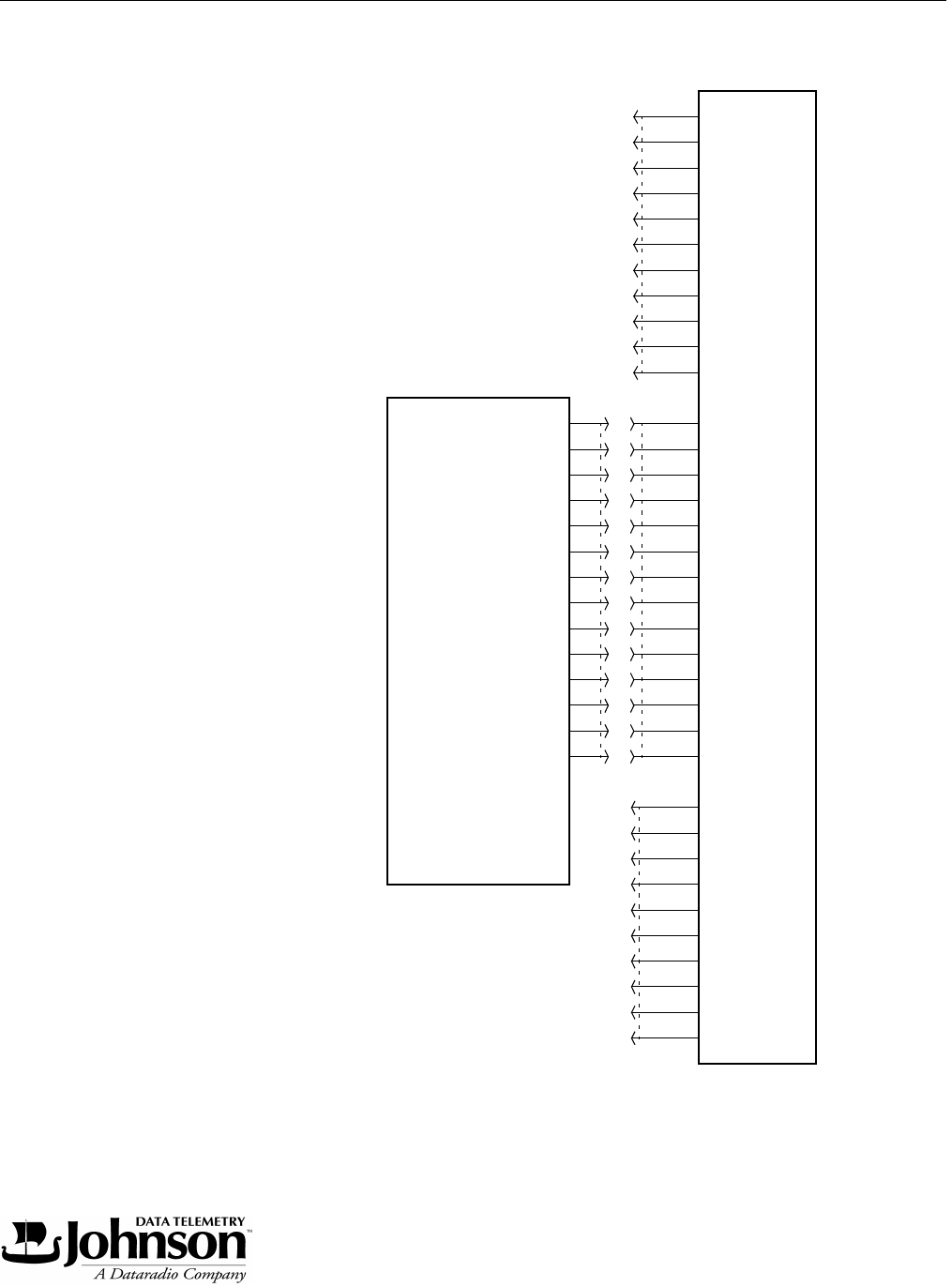
SCHEMATICS AND COMPONENT LAYOUTS
8-2
Part No. 001-3422-003
Figure 8-1 3422 INTERCONNECT
SYNTH DATA
GROUND
RSSI
TX IN
SYNTH LOCK
SYNTH ENABLE
SYNTH CLOCK
CARRIER DETECT
RX OUT
NC
GROUND
SYNTH LOCK DETECT
SYNTH ENABLE
SYNTH DATA
SYNTH CLOCK
DEMOD
J1
WIDE BAND OUT
RSSI
AUDIO OUT
GROUND
AUDIO IN
CARRIER DETECT
PTT
WIDE BAND IN
12
11
1
2
3
4
5
6
7
8
9
10
13
14
MOD
RSSI IN
RSSI IN
NC
FREQ SEL
1
2
3
4
5
6
7
8
9
10
1
2
3
4
5GROUND
RX DATA
TX DATA
NC
CONNECTOR
PROGRAMMING
USER INTERFACE
LOADER BOARD
RF BOARD
J104
11
6
7
8
9
10 GROUND
GROUND
NC
PRG0
PRG1
PRG2
PRG3
P101
J102
+13.6V DC
+13.6V DC IN
+7.5V DC SWITCHED
+5V DC SWITCHED
+5V DC OUT
+13.6V DC SWITCHED
+13.6V DC TX
+5V DC RX
+5V DC
023-3412-330
023-3412-030

SCHEMATICS AND COMPONENT LAYOUTS
8-3
Part No. 001-3422-003
Figure 8-2 TRANSCEIVER COMPONENT LAYOUT (COMPONENT SIDE VIEW)
Figure 8-3 TRANSCEIVER COMPONENT LAYOUT (OPPOSITE COMPONENT SIDE VIEW)

SCHEMATICS AND COMPONENT LAYOUTS
8-4
Part No. 001-3422-003
Figure 8-4 SCHEMATIC