CalAmp Wireless Networks BDD4T83-2 Paragon PD User Manual TITLE
CALAMP WIRELESS NETWORKS INC. Paragon PD TITLE
updated preliminary users manual

ParagonPD
Data Base Station
Technical Manual
Version 3.02
PRELIMINARY, For Internal Use Only
The entire contents of this manual and the Radio Installation Software
described in this manual are copyright 2002 by DATARADIO Inc.
Copyright DATARADIO Inc.
August 2002
Part no.: 120 20170-302
120 20170-302 ii ParagonPD Technical Manual
Table of Contents
1. PRODUCT OVERVIEW................................................................................................................................... 3
1.1 GENERAL DESCRIPTION .................................................................................................................................... 3
1.1.1 Features:................................................................................................................................................. 3
1.2 FACTORY TECHNICAL SUPPORT........................................................................................................................ 4
1.3 PRODUCT WARRANTY ...................................................................................................................................... 4
1.4 REPLACEMENT PARTS....................................................................................................................................... 4
1.4.1 Factory Repair........................................................................................................................................ 4
1.5 PACKAGING ...................................................................................................................................................... 5
2. INSTALLATION ............................................................................................................................................... 5
2.1 OVERVIEW........................................................................................................................................................ 5
2.2 LOCATION......................................................................................................................................................... 5
2.3 ELECTRICAL...................................................................................................................................................... 5
2.3.1 Radio Assembly Power............................................................................................................................ 8
2.3.2 BDLCPD assembly Power ........................................................................................................................ 9
2.4 ANTENNA ......................................................................................................................................................... 9
2.4.1 Overview ................................................................................................................................................. 9
2.4.2 Cabling and Connection ......................................................................................................................... 9
2.5 COMPLETING THE PHYSICAL INSTALLATION...................................................................................................... 9
2.6 CHECKING OUT NORMAL OPERATION ............................................................................................................. 10
3. OPERATING DESCRIPTION ....................................................................................................................... 10
3.1 RADIO ASSEMBLY........................................................................................................................................... 10
3.1.1 Front panels.......................................................................................................................................... 10
3.1.1.1 Receiver module............................................................................................................................................10
3.1.1.2 Exciter module ..............................................................................................................................................11
3.1.1.3 Power Amp module.......................................................................................................................................11
3.1.1.4 Speaker panel ................................................................................................................................................12
3.1.1.5 Dual Power Supply module...........................................................................................................................12
3.1.1.5.1 Rear Connections......................................................................................................................................12
3.1.2 Radio Assembly, rear panel .................................................................................................................. 13
3.1.2.1 Backplane PCB .............................................................................................................................................13
3.2 BDLCPD ......................................................................................................................................................... 13
3.2.1 BDLCPD Front panel............................................................................................................................. 13
3.2.1.1 Front Switches...............................................................................................................................................13
3.2.1.1.1 Reset.........................................................................................................................................................13
3.2.1.1.2 PF 1 ..........................................................................................................................................................13
3.2.1.2 Clearing Errors..............................................................................................................................................14
3.2.1.3 Test Transmissions........................................................................................................................................14
3.2.1.4 RS-232 LED Function Selection...................................................................................................................15
3.2.1.5 LEDs and Indications....................................................................................................................................15
3.2.1.5.1 Radio Network Indicators.........................................................................................................................15
3.2.1.5.2 RS-232 Port Indicators.............................................................................................................................16
3.2.1.5.3 Check and Power LEDs............................................................................................................................16
3.2.1.5.4 Alarm Indicators.......................................................................................................................................16
3.2.2 BDLCPD Rear panel .............................................................................................................................. 17
3.2.2.1 RS-232 Signal Levels....................................................................................................................................17
3.2.2.2 Pin Functions.................................................................................................................................................17
4. TROUBLE-SHOOTING AND TESTING ..................................................................................................... 19
4.1 EQUIPMENT REQUIRED ................................................................................................................................... 19
4.2 RECOMMENDED CHECKS................................................................................................................................19
4.3 ADDITIONAL TEST DETAILS ............................................................................................................................. 23
4.3.1 RF Data Link Test................................................................................................................................. 23
120 20170-302 iii ParagonPD Technical Manual
4.3.2 Carrier deviations ................................................................................................................................. 23
5. RADIO PROGRAMMING AND ADJUSTMENTS..................................................................................... 24
5.1 SERIES II RADIO PROGRAMMING .................................................................................................................... 24
5.1.1 Recommended Items.............................................................................................................................. 24
5.1.2 Module Programming........................................................................................................................... 24
5.1.3 Channel Selection via DIP Switches..................................................................................................... 27
5.2 SERIES II RADIO TUNING ................................................................................................................................28
5.2.1 Test Equipment...................................................................................................................................... 28
5.2.2 Receiver module (T885-xx-0200, T855-xx-0250 & T835-xx-0200) ...................................................... 29
5.2.2.1 Initial Setup...................................................................................................................................................29
5.2.2.2 Synthesizer Alignment ..................................................................................................................................29
5.2.2.3 Front-End Alignment ....................................................................................................................................30
5.2.2.4 SINAD and Linearity Check .........................................................................................................................30
5.2.2.5 RSSI Adjustment...........................................................................................................................................31
Exciter Module (T881-xx-0200,T857-xx-0250 or T837-xx-0200)......................................................................32
5.2.3.1 Initial Setup...................................................................................................................................................32
5.2.3.2 Synthesizer Alignment ..................................................................................................................................32
5.2.3.3 TX Frequency Error Adjustment...................................................................................................................33
5.2.3.4 Low-Frequency Balance Adjustment ............................................................................................................33
5.2.3.5 Exciter Power Output....................................................................................................................................34
5.2.4 Power Amplifier Module (T889 (800-870 MHz only), T859 or T839).................................................. 34
5.2.4.1 Power Amplifier Power Output.....................................................................................................................34
5.2.4.2 Forward Power Alarm Level (Optional setting) ............................................................................................35
5.2.4.3 Reverse Power Alarm Level (Optional setting).............................................................................................35
5.2.4.4 Tait T859 (UHF) Standard Tuning Procedure...............................................................................................35
5.2.4.5 Tait T859 Tuning for Best Efficiency............................................................................................................35
5.2.5 (TPL) LMS series Power amplifier (PA8-2BF-LMS) (890-960 MHz)................................................... 36
5.2.5.1 Power Output alignment (from TPL Communications).................................................................................36
5.2.5.2 Forward Power Alarm Level .........................................................................................................................36
5.2.5.3 Amplifier Activation......................................................................................................................................36
5.2.5.4 RF Input (Relative Reading) .........................................................................................................................36
5.2.5.5 Forward Power meter calibration ..................................................................................................................36
5.2.5.6 Reverse Power meter calibration...................................................................................................................36
5.2.5.7 Reverse Power Alarm Level..........................................................................................................................37
6. SPECIFICATIONS.......................................................................................................................................... 45
APPENDIX 1 - PARAGONPD DEVIATION ADJUST ........................................................................................................ 44
FIGURE 1 - TYPICAL RADIO AND POWER SUPPLY ASSEMBLIES, FRONT VIEW................................................................... 6
FIGURE 2 - BDLCPD, FRONT VIEW ................................................................................................................................. 6
FIGURE 3 - TYPICAL RADIO AND POWER SUPPLIES ASSEMBLY, REAR VIEW..................................................................... 7
FIGURE 4 - BDLCPD, REAR VIEW................................................................................................................................... 7
FIGURE 5 - BDLCPD’S REAR CONNECTION, SWITCH, AND FUSE ..................................................................................... 9
FIGURE 6 - RECEIVER MODULE FRONT PANEL.............................................................................................................. 10
FIGURE 7 - EXCITER MODULE, FRONT PANEL............................................................................................................... 11
FIGURE 8 - POWER AMP MODULE, FRONT PANEL ......................................................................................................... 11
FIGURE 9 - SPEAKER PANEL......................................................................................................................................... 12
FIGURE 10 - DUAL POWER SUPPLY REAR CONNECTIONS.............................................................................................. 12
FIGURE 11 - BDLCPD MEMBRANE SWITCHES............................................................................................................... 13
FIGURE 12 - RF INDICATORS........................................................................................................................................ 15
FIGURE 13 - RS-232 PORT LED INDICATORS................................................................................................................ 16
FIGURE 14 - ALARMS LED INDICATORS.................................................................................................................... 16
FIGURE 15 - BDLCPD Y CABLE AND PINOUT ............................................................................................................... 18
FIGURE 16 - CARRIER DEVIATIONS FOR TONE OR DATA MODULATION........................................................................ 23
120 20170-302 iv ParagonPD Technical Manual
FIGURE 17 - RECEIVER SYSTEM INFORMATION............................................................................................................ 25
FIGURE 18 - RECEIVER CHANNEL INFORMATION SCREEN............................................................................................ 25
FIGURE 19 - EXCITER SYSTEM INFORMATION SCREEN................................................................................................. 26
FIGURE 20 - EXCITER CHANNEL INFORMATION SCREEN .............................................................................................. 26
FIGURE 21 - BACKPLANE DIP SWITCHES EXAMPLE - CHANNEL 5 SELECTED ............................................................... 27
FIGURE 22 - T855 AND T885, TYPICAL RSSI CURVE: VOLT TO DBM.......................................................................... 31
FIGURE 23 - T835, TYPICAL RSSI CURVE: VOLT TO DBM........................................................................................... 31
FIGURE 24 - T800-50-0001 BACKPLANE ..................................................................................................................... 32
FIGURE 25 - T859 TUNING SETTINGS .......................................................................................................................... 35
FIGURE 26 - (TPL) LMS REAR PANEL ........................................................................................................................ 37
FIGURE 27 - T885-0020 RECEIVER TUNING CONTROLS LOCATION ............................................................................. 38
FIGURE 28 - T881-0200 EXCITER TUNING CONTROLS LOCATIONS.............................................................................. 39
FIGURE 29 - T855 RECEIVER TUNING CONTROLS LOCATION ...................................................................................... 40
FIGURE 30 - T857 EXCITER TUNING CONTROLS LOCATIONS....................................................................................... 41
FIGURE 31 - T835 RECEIVER TUNING CONTROLS LOCATION ...................................................................................... 42
FIGURE 32 - T837 EXCITER TUNING CONTROLS LOCATION......................................................................................... 43
TABLE 1 - POWER SUPPLY LEDS INDICATIONS.............................................................................................................. 8
TABLE 2 - TX MODE SELECTION LEDS INDICATIONS................................................................................................... 14
TABLE 3 - TEST TRANSMISSIONS ................................................................................................................................. 14
TABLE 4 - RS-232 LED FUNCTION SELECTION SEQUENCE ......................................................................................... 15
TABLE 5 - RS-232 SIGNAL LEVELS .............................................................................................................................. 17
TABLE 6 - DTE PORT 9-PIN FUNTIONS......................................................................................................................... 17
TABLE 7 - DTE PORT 25-PIN FUNCTIONS..................................................................................................................... 17
TABLE 8 - CHECKLIST A (AFTER INSTALLATION) ......................................................................................................... 20
TABLE 9 - CHECKLIST B (GENERAL) ........................................................................................................................... 21

120 20170-302 vParagonPD Technical Manual
WHAT'S NEW
History
Version 3.02- Preliminary, September 2002
- Corrections of xRC4FSK modulations for VHF radios.
Version 3.01- Preliminary, August 2002
- Introduction of xRC4FSK modulations for VHF and 900 MHz radios.
- "RADIO PROGRAMMING AND ADJUSTMENTS" and "Specifications" sections
revised.
Version 3.0, June 2002
- Introduction of 32kb/s
- Support Series II VHF, UHF and 800/900 MHz radios.
- This version does not support Series I 800 MHz radios, refer to
previous technical manual versions.
- "RADIO PROGRAMMING AND ADJUSTMENTS" and "Specifications" sections
revised.
Version 2.0: May 2001
• First release covering, in addition to the DGMSK model, the SRRC4FSK
modulated model with speeds of up to 25.6 Kbps. Relevant changes
made to:
- Section 1.2.1 “Features”
- Section 1.5.2 “Model Designation”
- Table 3 “Test transmissions”
• This version introduces the following changes:
- Section 1.6 “Radio Series I or II:
- Revised description
- Section 2.3 “Electrical”:
- Clarification of amperage requirement
- Figure 4 “BDLCPD, rear view”. Re-tracing of top fan wiring to cor-
respond to factory routing.
- Section 3.1.1 “Receiver”:
- Endnote added to clarify troubleshooting characteristic.
- Section 3.1.1.5 “Dual Power Supply”, clarification of “OL” (over-
load) LED function.
- Figure 10 “Dual Power Supply Rear Connection” corrected to corre-
spond to the voltage printed on the connector label.
- Section 4 “WinRIS” program detailed.
120 20170-302 vi ParagonPD Technical Manual
- Table 8 “Carrier deviations for Tone or Data Modulation”. Now in-
corporates in a single table the details previously available as
Table 8 and Table 10.
- Table 10 “Checklist B, (General)”, steps 6 and 7 revised to merge
values for the two models.
- Table 11 “Checklist B, (ParagonPD)” steps 6,7 and 10 revised
- Figure 20 “Channel Selection via internal DIP switches”, clari-
fies the use of switch 8.
- Section 6.2.3.5 and 6.4.3.5 “Exciter Power Output” correction of
output power to 4 Watts.
- Figure 21 “T885 Receiver tuning control location”, clarification
of RSSI test point location.
- Section 7 “Specifications”:
- Rx and Tx “Current Consumption” values revised.
- Base Station “Power Consumption” specification added.
• Supersedes ParagonPD Addendum 124 20170-001a, dated February 2001.
• Supersedes Technical Support Bulletin TSB ATL007, dated 17 April,
2001 and titled “New Deviation Settings for 800MHz GeminiPD and Para-
gonPD with 4 level FSK Modulation”.
Version 1.0: May 2000
• First released version, DGMSK modulated model, and speeds up to
19200 b/s.
120 20170-302 vii ParagonPD Technical Manual
Definitions
The following terms are used throughout this document.
Asynchronous Information that can be sent at random times, and not synchronized to a clock.
Transmission characters begin with a “start” bit and end with a “stop” bit.
AVL Automatic Vehicle Location. Optional feature that involves using GPS (Global
Positioning System) signals from the mobile unit by the Host PC.
BDLCPD Base Station Data Link Controller (PD = Parallel decode). An async radiomo-
dem designed to control the base station in mobile systems. A component of
ParagonPD.
DBA Dataradio’s Dynamic Bandwidth Allocation protocol designed for short-
inquiry/long response applications such as dispatch systems. Latest enhance-
ments include support for occasional long messages inbound, and for Out-of-
Band data for AVL reports with no extra overhead.
DCE Data Communications Equipment. This designation defines the direction (input
or output) of the various RS-232 interface signals. Modems are always wired as
DCE.
DTE Data Terminal Equipment. This designation defines the direction (input or out-
put) of the various RS-232 interface signals. Most user equipment, as well as
PCs, are wired as DTE.
GeminiPD High specs mobile radiomodem. (PD = Parallel Decode)
GeminiPD+ On-air compatible with GeminiPD. Runs up to 32 kb/s
Network Speed This is the bit rate on the RF link between units. Could be different from COM
port baud rate.
ParagonPD Factory-integrated industrial-grade data base station using Parallel Decode tech-
nology. Used in VIS mobile networks.
Parallel Decode Technology featuring dual receivers for added data decode sensitivity in multi-
path and fading environments.
Refarming FCC’s strategy for using the radio spectrum more efficiently to meet future
communications requirements.
Radio Assembly Radio modules used in ParagonPD and available in two distinct series depending
on radio’s frequency band.
RS-232 Industry–standard interface for serial data transfer.
VIS Vehicular Information Solutions. Dataradio’s name for a series of products spe-
cially designed for mobile data.
WinRIS Windows Radio Installation Software. This software allows basic tests, unit con-
figuration, and troubleshooting.

120 20170-302 Paragon
PD
Technical Manual
3
1. PRODUCT OVERVIEW
This document provides the information re-
quired for the setting up, operation, testing and
trouble-shooting of the DATARADIO ParagonPD
radio-modem base station. Intended Audience
This document is intended for engineering, in-
stallation, and maintenance personnel.
1.1 General Description
ParagonPD product is a factory-integrated
industrial-grade data base station used in mobile
networks and is designed specifically to fit the
needs of vehicular applications.
It features dual receivers for added data decode
sensitivity in multi-path and fading environ-
ments.
When used with Dataradio’s state-of-the-art
GeminiPD/PD+ mobile data solution, the system
delivers unequaled high-speed data performance
and unmatched effective throughput.
All ParagonPD models are supplied in a rack-
mount configuration that includes:
• A ParagonPD full-duplex Radio assembly
• A contemporary, high-speed Dataradio
“Base Station Data Link Controller”
(BDLCPD).
ParagonPD units do not include the optional wire
line modem(s). Duplexer and backup power units
are custom furnished items. The laptop PC and its
application software are user-supplied items.
1.1.1 Features:
• Parallel Decode (PD) technology featuring
dual receivers for added decode sensitivity
in multi-path and fading environments.
• Sophisticated DSP-based modem design
provides added system performance, fewer
retries and more effective throughput.
• Models with on-air data speeds and modu-
lation types as follows:
Channel spacing
Modulation
type 12.5 kHz
NPSPAC
&
900MHz
25 kHz
9.6 kb/s 9.6 kb/s 9.6 kb/s
DGMSK1
8.0 kb/s 8.0 kb/s 19.2 kb/s
16 kb/s 19.2 kb/s 32 kb/s2
xRC4FSK1
14.4 kb/s 16 kb/s 25.6 kb/s
• Available in 800 MHz, UHF and VHF
• Power output of 20W to 70W for
ParagonPD’s 800 MHz and of 20W to 100W
for UHF and VHF
• Supports high-efficiency Dataradio DBA
over-the-air protocol
• Over-the-air compatible with MobilPac/R
GeminiPD mobile products
• Modular design in a rugged die-cast alumi-
num chassis
• ParagonPD units are factory-configured
based on each customer’s network system
requirements
• EEPROM Flash programmable firmwares
1 Networks must use common modulation, bit and
baud rates.
2 Available with Gemini PD+ only

120 20170-302 Paragon
PD
Technical Manual
4
1.2 Factory Technical Support
The Technical Support departments of
DATARADIO provide customer assistance on
technical problems and serve as an interface
with factory repair facilities. They can be
reached in the following ways:
For Canada and International customers:
DATARADIO Inc.
5500 Royalmount Ave, suite 200
Town of Mount Royal
Quebec, Canada H4P 1H7
Technical support hours: Monday to Friday 9:00
AM to 5:00 PM, Eastern Time
phone: +1 514 737-0020
fax: +1 514 737-7883
Email address: support@dataradio.com
or
For U.S. customers:
DATARADIO Corp.
6160 Peachtree Dunwoody RD., suite C-200
Atlanta, Georgia 30328
Technical support hours: Monday to Friday 8:30
AM to 5:30 PM, Eastern Time
phone: 1 770 392-0002
fax: 1 770 392-9199
Email address: drctech@dataradio.com
1.3 Product Warranty
Warranty information may be obtained by con-
tacting your sales representative.
1.4 Replacement Parts
This product is usually not field-serviceable,
except by the replacement of individual radio
modules. Specialized equipment and training is
required to repair logic, modem boards and ra-
dio modules.
Contact Technical Support for service informa-
tion before returning equipment. A Technical
Support representative may suggest a solution
eliminating the need to return equipment.
1.4.1 Factory Repair
When returning equipment for repair, you must
request an RMA (Returned Material Authoriza-
tion) number. The Tech Support representative
will ask you several questions to clearly identify
the problem. Please give the representative the
name of a contact person, who is familiar with
the problem, should a question arise during
servicing of the unit.
Customers are responsible for shipping charges
for returned units. Units in warranty will be re-
paired free of charge unless there is evidence of
abuse or damage beyond the terms of the war-
ranty. Units out of warranty will be subject to
service charges. Information about these charges
is available from Technical Support.
120 20170-302 Paragon
PD
Technical Manual
5
1.5 Packaging
Each ParagonPD product normally leaves the
factory packaged as follows:
• A Series II Dataradio base station “Radio
assembly”
• A dual power supply assembly
• A Dataradio BDLCPD model
• A Radio Interface Cable to link the Radio
assembly to the BDLCPD:
18-inch long “Y” cable; DB-25 female to
dual DB-25 female (p/n 730 03374-102) for
connection between backplane PCBs and
BDLCPD.
• One standard seven-foot 120VAC power
cord
• Two DC power cables to connect the radio
assembly to the dual power supply assem-
bly.
• Courtesy small parts kit
Frequently, ParagonPD product components are
field-assembled prior to customer delivery.
The cabinetry may then be supplied in one of
several custom rack-mount configurations that
may also include fan, backhaul modems,
duplexer/filters/combiners, and ancillary
equipment.
If damage has occurred to the equipment during
shipment, file a claim with the carrier immedi-
ately.
2. Installation
2.1 Overview
The cabinet and rack-mount housing the
ParagonPD’s radio assembly and the BDLCPD is
generally installed in a sheltered facility.
Occasionally located adjacent to the nerve
center of the user’s network, it is often located
near tower sites or at remote locations where it
operates unattended.
Furnishings needed include power, cabling, and
installation of antenna, landline or microwave
modem, and host PC or portable computer. De-
tails of these are outside the scope of this man-
ual. This manual covers the radio assembly and
the BDLCPD that includes the modem.
2.2 Location
Be sure to place the ParagonPD in such a way
that:
• The LEDs can be seen (as an aid in trouble-
shooting)
• Access to the antenna connector and to the
back connectors is possible without remov-
ing the unit
• Sufficient air may flow around the unit to
provide adequate cooling.
2.3 Electrical
Standard 120 VAC electrical power is required.
It should be capable of providing at least 10A to
power ParagonPD (<6A) and ancillary equip-
ment.
120 20170-302 Paragon
PD
Technical Manual
6
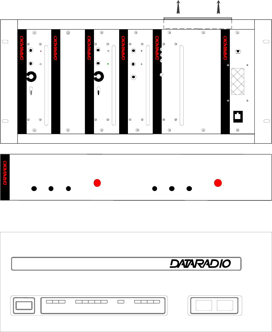
Figure 1 - Typical radio and power supply assemblies, front view
Figure 2 - BDLCPD, front view
RESET
UFLFRMLMCK
ALARMSRF
TXRXCS
S-3
RS-232
CM FR FT RD TD
123
PF1
®
Re c e i v e r
®
Gating Gate
Line
Le vel Su pp l y
®
Ex c i t e r
Ca r r i e r On
Line
Se n s i t i vi t y
Supply
Microphon e
®
Pow er Am p li fi er
Low Forward Power
Supply
Hi gh Re ver se Power
Pow er
Sensitivity
Monitor
Volume
Off
On
Monitor
Mute
Re c e i v e r
Gating Gate
Line
Le vel Supply
Sensitivity
Monitor
Volume
Off
On
Monitor
Mute
Excellence in Radio
C omm unic at ion s
®
®
Speaker Panel
programming
port
RX2RX1
OFF
SP EAK ER
SELE CT SWI TCH
Air Flow
OL Stby On Power
OL Stby On Power
T800 II Slimline
®
Dual Power Supply Module
120 20170-302 ParagonPD Technical Manual
7
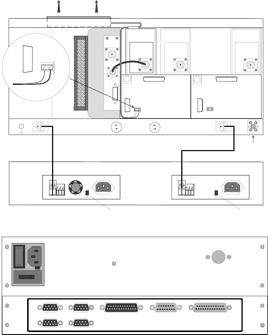
Figure 3 - Typical radio and power supplies assembly, rear view
Figure 4 - BDLCPD, rear view
Employer uniquement avec
un fusible de 250 V
Use on l y wit h a 250 V f u se
DEV. 3 RS-2 32
DEV. 5 RS-232
DEV. 2 RS-232
DEV. 4 RS-232
DEV. 1 RS-232 DEV. 6 DIG. I/O EXT. RADIO/TEST
T808-10-00CA T807-10-00CA
REAR VIEW
Air Flow
GND
DC
INPUT 1
FUSE 1FUSE 2DC
INPUT 2 13.8 VDC
2 AMPS MA
X
F
U
S
EF
U
S
E
FU
S
E
F
U
S
EF
U
S
E
FU
S
E
+-+-+-+-
GND
GND
T800-50-0001
No 1
PL1
SK5
T800-50-0001
No 2
PL1
SK5
_
+
_
+
SK5
_
+
FAN
CN
2
120 20170-302 ParagonPD Technical Manual
8
2.3.1 Radio Assembly Power
Referring to Figure 3, the Radio assembly unit
receives two separate 13.8 VDC power inputs
from a “T800 Slimline” dual power supply typi-
cally rack-mounted right below the main assem-
bly radio chassis.
The T800 is made up of two separate power sup-
ply units joined in a single chassis:
• A T807 using convection cooling is rated up
to 15A at 13.8VDC. It supplies all the radio
modules other than the Power Amplifier.
• A T808 using convection and fan cooling is
rated up to 25A at 13.8VDC. It supplies only
the Power Amplifier module.
Normally used at room ambient temperatures,
they can operate within their specifications over a
range of –10 to +60 °C.
Note: Internal over-temperature protection shuts
down the main transformer above 105
degrees Celsius.
Both power supply modules are internally con-
nected to ground via their individual, rear-
connected, seven-foot standard 120 VAC power
cords. Nevertheless, each requires a separate se-
cure electrical ground connection. Individual
grounding tabs are provided next to the power
connectors.
Similarly, the Radio Assembly chassis requires a
secure ground connection. A threaded grounding
binding post fitted with a knurled binding-nut is
provided on the chassis next to DC input 2.
Separate grounding leads with appropriate con-
nectors are supplied (either in the courtesy small-
parts kit or with one end fastened to the equip-
ment.
For each of the power supply modules:
1. Fit one end of the grounding lead’s push-
on connector onto the grounding tab.
For the Radio Assembly chassis:
1. Install the grounding lead’s lug over the
binding post and firmly hand-tighten the
binding-nut.
For both A and B
2. Fit the slotted connector (on the other
end of each of the grounding connector)
under a conveniently located screw on
the rack frame or other support surface.
Scrape away paint if needed to ensure
clean contact.
3. Apply anti-corrosion compound where
paint scraping was done.
4. Ensure by testing continuity that a secure
electrical and mechanical connection is
achieved.
If a –DC rail (0V) is installed as part of the sys-
tem, the grounding leads may alternatively be
fitted to the rail terminal.
Caution:
Improper grounding between power supply case
and rack frame may result in harmful voltage
potentials and/or miscellaneous power supply
switching noise problems in both receivers and
transmitter.
Press both red power buttons located on the front
of the module to have complete power distribu-
tion to the Radio assembly.
The power supply front panel LEDs indications
are:
Table 1 - Power Supply LEDs Indications
LED Color Indication
On Green Power enabled *
Stby Red Power disabled *
OL Steady Red Current Overload
On & OL Flashing green and
red respectively Over voltage
* To remove voltage from the power supply PCB, disconnect
the main power cords.
For LEDs descriptions, see section 3.2.1.5
The Radio assembly is fused at the rear of the
chassis:
• Fuse 1 is a 32-volt MDL (slow-blow) 10A
• Fuse 2 is a 32-volt MDL (slow-blow) 30A
Note: the fuses form factor and their locations
may differ from Figure 3.
120 20170-302 ParagonPD Technical Manual
9
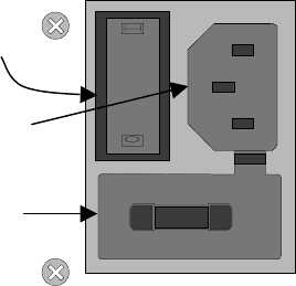
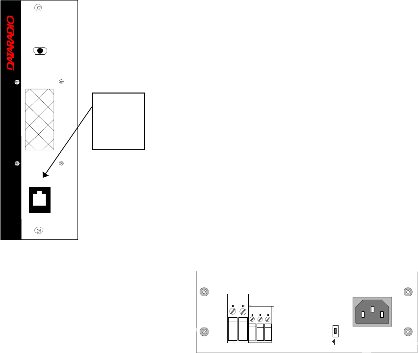
2.3.2 BDLCPD assembly Power
The BDLCPD assembly uses a standard 120 VAC
power cord. Plug this cord to the rear power out-
let shown in Figure 4 and Figure 5.
To check or install a fuse:
1. Open the slide-out fuse drawer located below
the power connector by using a fine bladed
screwdriver or a knife blade and gently pry
open.
2. Hold the fuse support in one hand and with
the other, lift the center plastic retainer until
it releases the fuse sliding base.
3. Replace or install a 250V, 2A fuse.
4. To complete the procedure, push the sliding
fuse base until it snaps under the retainer.
5. Re-insert the fuse drawer in its housing and
push until it is fully seated and closed.
When ready to apply power, use the ON-OFF
toggle power switch adjacent to the power con-
nector.
Figure 5 - BDLCPD’s rear connection, switch, and fuse
2.4 Antenna
2.4.1 Overview
ParagonPD commonly uses three antennas (one
transmit and two receive) unless a duplexer is
used with one of the receive antennas; then only
two antennas would be needed. They should be
mounted according to any guidelines supplied
with the antennas. For antennas placement and
spacing, consult System Engineering.
2.4.2 Cabling and Connection
1- Route good quality 50-ohm double-shielded
coaxial cable(s) (e.g. RG-214 or Heliax) from
the selected antenna position(s) to the Para-
gonPD Radio assembly.
2- Terminate the RX-1 and RX-2 cable ends at
the Receiver modules rear position with an
N-type connector.
3- Similarly, terminate the TX cable end at the
Power Amp’s module rear position with an
N-type connector.
Caution:
When terminating RF cables use brand-name
crimping tools (such as AMP, Jensen,
CrimpMaster, etc…) of the correct size for
the cable and type of connector used.
Common pliers are NOT acceptable.
2.5 Completing the physical
Installation.
ParagonPD products are factory-configured to
user’s requirements and are shipped ready to run.
After new installations:
• Re-check that all connections are secure on
radio and BDLCPD assemblies (antennas, PC,
power cords etc.)
• Check that fuses are inserted.
• Turn both BDLCPD and radio power ON.
You are now ready to check for normal operation
(as per paragraph 2.6) and to run the Dataradio
Windows Radio Installation Software (WinRIS)
program for testing or trouble-shooting.
Any change(s) to the settings must be done via
files saved on diskette and loaded into the unit
using the WinRIS program.
E mp l oye r u ni qu em ent av ec
un fu sible de 25 0 V
Use only with a 250 V fu se
ON-OFF
Switch
120VAC
Connector
Fuse
Slide-out
Drawer
120 20170-302 ParagonPD Technical Manual
10
2.6 Checking out Normal
Operation
1- Check that power is applied.
2- Check Radio assembly lights for proper
operation as per section 3.1.1
3- Check for proper operation of the BDLCPD’s
LEDs as per section 3.2.1.5.
4- Using the WinRIS program and an in-line
wattmeter, check forward & reverse power to
confirm main antenna installation (as per
section 4)
5- Using WinRIS, check the RF Data Link with
a mobile that can be heard (as per section
4.3.1)
If user application and mobiles are available, test
the installation by going through a normal
sequence of transmitting and receiving messages.
3. Operating Description
3.1 Radio Assembly
The Radio assembly component of each Paragon
product is made up of high performance
synthesized radio base station designed for single
operation. Referring to Figure 1 on page 6, the
Radio Assembly’s modules are commonly
installed in a standard, 19-inch wide rack frame.
3.1.1 Front panels
The complement of modules is identical for
Series II VHF, UHF, and 800/900 MHz models:
• 2 x Receivers
• 1 x Exciter
• 1 x Power Amplifier
• 1 x Speaker panel
• 1 x Dual Power Supply
3.1.1.1 Receiver module
The RX1 and RX2 receivers’ use identical front
panel controls and indicators. These are:
• Gating Sensitivity - sets the RF signal level
required to open the mute gate and allow
audio to pass to the speaker1.
• Gate LED - indicates the status of the mute
circuit. It is lit when a signal above the mute
threshold is received1.
• Supply LED - is lit when DC power is applied.
Fast Flashes when linked with PGM800Win.
Slow Flashes indicates VCO (synthesizer) out of
lock. Unequal Flashes indicates internal commu-
nication error.
• Line Level - Not used
• Monitor Volume - The audio output delivers up
to 1 watt to the speaker. Always set volume knob
to minimum when not in use to reduce current
consumption.
• Monitor Mute Switch - opens the mute, allowing
continuous monitoring of the audio signal.
On = audio muted
Figure 6 - Receiver module front panel
1 “Gating Sensitivity” and “Gate LED” are not
functionally used except to allow listening to in-
coming receptions as a trouble-shooting aid.
Depending on the sensitivity adjustment, the Gate
LED lights and a relay can be heard on incoming
RF signals.
Gating
Sensitivity
Gate
LED
Line
Level
Monitor
Volume
Monitor
Mute
On - Off
Receiver
®
Gating Gate
Line
Level Supply
Sensitivity
Monitor
Volume
Off
On
Monitor
Mute
120 20170-302 ParagonPD Technical Manual
11
3.1.1.2 Exciter module
The Exciter’s front panel controls and indicators
are:
Figure 7 - Exciter module, front panel
• Carrier Switch - momentarily keys the trans-
mitter ON while pressed (used for test pur-
poses only).
• On LED - is lit when transmitting
• Line Sensitivity – not used.
• Supply LED - is lit when DC power is ap-
plied. Fast Flashes when linked with
PGM800Win. Slow Flashes indicates VCO
(synthesizer) out of lock. Unequal Flashes
indicates internal communication error.
• Microphone Socket – not used.
3.1.1.3 Power Amp module
The Power Amp front panel and indicators are:
Figure 8 - Power Amp module, front panel
• Supply LED - is lit when DC power is ap-
plied.
• Low Forward Power LED - is lit when for-
ward power is below the level set, normally
80% of nominal forward power.
• High Reverse Power LED - is lit when high
reverse power is detected (e.g. VSWR= 3:1).
• Power - sets the PA output power:
- VHF & UHF models: 20 - 100 Watts
- 800 model: 20-70 Watts
Carrier
Switch
On
LED
Supply
LED
Line
Sensitivity
Microphone
Socket
®
Exciter
Carrier On
Line
Sens itivity
Supply
Microphone
®
Power Amplifier
Low Forward P ower
Supply
High Rev erse Power
Pow er
Supply
LED
Low Forward
Power LED
High Reverse
Power LED
Power
Adjustment
120 20170-302 ParagonPD Technical Manual
12
3.1.1.4 Speaker panel
Referring to Figure 9, the speaker panel is fitted
with a four Ω speaker.
Both series of radio assemblies share the same
front panel fitted with an RJ11 connector. This
connector is used to allow programming the radio
from the front of the unit via a programming
lead. This feature is exclusive to the Series II
modules.
If the speaker panel needs to be removed, a mir-
ror programming port connector is provided on
both backplanes.
Figure 9 - Speaker panel
3.1.1.5 Dual Power Supply module
The Dual Power Supply module is made up of
two separate power supply units coupled in a sin-
gle chassis.
Refer to Table 1 on page 8 for tabular listing of
power supply LEDs indicators.
Refer to Figure 1 for the front panel LED layout.
This module has:
• Two “Power” red-colored pushbutton
switches - Push in for ON and release out for
OFF. Control complete power distribution to
the Radio assembly
• Two “ON” LEDs - light green when push
button(s) is (are) ON; DC power is distrib-
uted to radio modules. Flash green in con-
junction with the “OL” LED (flashing red)
when an over voltage condition is present.
• Two “Stby”- Standby voltage LED, lights red
when push button is off; AC power is applied
but DC is not distributed to radio modules.
To remove presence of voltage, disconnect
both power cords.
• Two “OL” LEDs - Monitor current overload,
light steady red when supply exceeds current
limit set; nominally 25Amps (T808 model).
Flashes red in conjunction with the ON LED
(flashing green) when an over voltage condi-
tion is present.
3.1.1.5.1 Rear Connections
Referring to Figure 10, (convection-cooled model
shown; fan-cooled model not illustrated), the rear
connections for each of the power supply are:
Fail Alarm –
Off: Power supply OK; approx. +Vout (via 1k
resistor - typ. 13.8V).
ON: Power supply failure; approx. -Vout (via
11k resistors - typ. 0V)
+ Remote – Not used for Paragon
- Sense – Not used for Paragon
-VE – main ground (0V)
+13.8V – Mains DC output supply
Figure 10 - Dual Power Supply rear connections
Note: more power supply installation details are
covered in section 2.3.1
®
S peaker Panel
programm ing
port
RX2RX1
OFF
SP EAK ER
SELE CT SWI TCH
Not
Used with
800 MHz
Series I
model
15A
+
-
Output
Sense
+
-
Remote
Fail Alarm
13.8V
Max.

120 20170-302 ParagonPD Technical Manual
13
3.1.2 Radio Assembly, rear panel
3.1.2.1 Backplane PCB
Referring to Figure 3, two main backplanes are
used. Their main components are:
• RJ11 connector – Mirrors the one on the
front of the Speaker panel (series con-
nected to both backplanes). Used for
programming the Radio Assembly when-
ever the speaker panel has been removed.
• DB-25M plug at PL1 (one side of the
“Y” cable on each PCB) – used to supply
the receive signal to the BDLCPD’s single
“EXT.RADIO/TEST” DB-25F plug.
• Two channel-select DIP switches (SW1
and SW2)
This feature is exclusive to the Series II model.
• Cooling fan driver – CN2 located on
backplane connects to the horizontally-
mounted fan on top of the Radio assem-
bly and activated by BDLC’s PTT signal.
• Coaxial relay driver – not used.
3.2 BDLCPD
The rack-mounted BDLCPD is housed in a steel
case. It has no user serviceable parts. Unit’s con-
figuration is stored in flash memory (EEPROM).
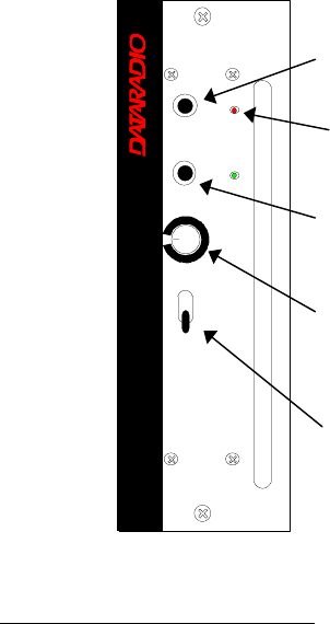
3.2.1 BDLCPD Front panel
Referring to Figure 2, the front panel of the
BDLCPD has two cutouts across its length.
A- The left cutout groups the unit’s type label
and ten LED indicators:
• The S3 label designates the BDLCPD as a
“three Serial-port” model
(Ports 4 and 5 are reserved for future use)
• The RF group of 3 LEDs
• The RS-232 group of 5 LEDs
• A single CK LED
• The ALARMS group of 4 LEDs
B- The right cutout groups two tactile (mem-
brane) switches (PF1 and RESET).
3.2.1.1 Front Switches
Referring to Figure 11, the BDLCPD uses two
membrane-type switches labeled:
• RESET
• PF 1
These switches indicate contact by emitting a
short BEEP tone when pressed.
Figure 11 - BDLCPD membrane switches
3.2.1.1.1 Reset
Pressing Reset produces the same result as pow-
ering OFF and ON again. It restarts the micro-
processor, the peripherals and invokes the on-
board diagnostics. BDLCPD’s radio modules’ in-
ternal flash-memories are read and their values
are loaded in system SRAM CPU flash-memory.
Normally, pressing Reset results in one short
BEEP tone followed by all LEDs coming ON for
about four seconds. Then, the LEDs flash in a
“ripple” pattern for close to two seconds indi-
cating diagnostics are in progress. At the end of
this period, all LEDs should be OFF except CK
that should flash about six to eight times per sec-
ond.
Expect an additional two seconds delay for CK to
start flashing and the UF indicator to come ON if
the radio assembly is not connected or not pow-
ered (see section 3.2.1.5.4 for Alarm details).
3.2.1.1.2 PF 1
PF 1 is a multi-function switch:
• It clears LED error indications
• It initiates test transmissions
• It sets the function of the RS-232 LEDs
PF1 RESET
120 20170-302 ParagonPD Technical Manual
14
3.2.1.2 Clearing Errors
Major and minor error LED indications remain lit
on the front panel until:
• The unit is RESET
• The unit is powered OFF and ON again
• PF 1 is pressed
The PF 1 switch can be pressed at any time to
clear an error display without affecting normal
operations.
3.2.1.3 Test Transmissions
To select a pattern and begin transmission, start
by pressing and holding PF1. It beeps once, all
five RS232 LEDs light; listen for a second beep
followed by a third beep. After two seconds, the
unit beeps and goes in “TX Select” mode with
only the three rightmost RS-232 LEDs now used
as selection indicators. Only release PF1 after the
third beep.
Following release:
• Start of selection must be made within two
seconds. If not, the unit will default to pattern
one and start test transmitting.
• PF1 may be pressed more than once. The
number of times it is pressed determines the
type of pattern that will be transmitted ac-
cording to Table 3.
• Each pressing of PF1 extends the two-second
timer.
• The three rightmost RS-232 LEDs display
are used to indicate TX mode selection as
shown in Table 2.
Table 2 - TX mode selection LEDs indications
Binary TX mode LED indications
TX pattern
selected FT LED RD LED TD LED
1OffOffOn
2 Off On Off
3 Off On On
4OnOffOff
5OnOffOn
6OnOnOff
7OnOnOn
Once the type of transmission is selected, stop
pressing PF1, allow the two-seconds timer to run
down. Automatically, the BDLCPD turns its
transmitter ON, sends the selected “test pattern”
for 55 seconds and turns its transmitter OFF. The
TX LED in the RF group of indicators lights in
red while test transmitting. Pressing PF1 while
the 55 seconds test is in progress stops the test.
At the end of test transmission, BDLCPD opera-
tion returns to normal and the RX LED lights in
green (monitoring normal transmitter activity).
Table 3 - Test Transmissions
DGMSK ParagonPD
# times
PF1 is
pressed 8000 b/s 9600 b/s 19200 b/s
1 2000 Hz
Dotting
2400 Hz
Dotting
4800 Hz Dotting
2
4000 Hz 4800 Hz 9600 Hz
3
100 Hz Square wave
4 Random data Random data Random data
5 Unmod Unmod Unmod
61000 Hz sine
beacon mode 1000 Hz sine
beacon mode 1000 Hz sine
beacon mode
71000 Hz sine wave
Adjustment tone
xRC4FSK ParagonPD
# times
PF1 is
pressed 32000
b/s 25600
b/s 19200
b/s 16000
b/s 14400
b/s
14000 Hz
Dotting* 3200 Hz
Dotting* 2400 Hz
Dotting* 2000 Hz
Dotting* 1800 Hz
Dotting*
2Do not
use Do not
use Do not
use Do not
use Do not
use
3100 Hz
Square
wave
100 Hz
Square
wave
100 Hz
Square
wave
100 Hz
Square
wave
100 Hz
Square
wave
4Random
data Random
data Random
data Random
data Random
data
5 Unmod Unmod Unmod Unmod Unmod
6
1000 Hz
sine
beacon
mode
1000 Hz
sine
beacon
mode
1000 Hz
sine
beacon
mode
1000 Hz
sine
beacon
mode
1000 Hz
sine
beacon
mode
7
1000 Hz
sine
wave
Adj. tone
1000 Hz
sine
wave
Adj. tone
1000 Hz
sine
wave
Adj, tone
1000 Hz
sine
wave
Adj, tone
1000 Hz
sine
wave
Adj, tone
* Dotting with reduced amplitude
Notes:
- For DGMSK models, a dotting pattern consists of an
alternating series of bits.
- For the xRC4FSK models, a dotting pattern consists of
an alternating series of bits where only the lowest-level
symbol’s modulation is used.
- The square wave is used to check transmitter low fre-
quency balance..
- Pattern 6 produces a transmission of approximately 55
seconds followed by about 55 seconds of silence.
Initial transmission in a sequence may be shorter than
55 seconds. TX LED stays steadily red for duration of
the test. Press PF1 to terminate beacon mode.
120 20170-302 ParagonPD Technical Manual
15
3.2.1.4 RS-232 LED Function Selection
The PF 1 button is used to select the RS-232 dis-
play mode as follows:
• If pressed ONCE (do not hold pressed):
- Clears Alarm indications
- CK LED stops flashing for 2 seconds
- During this time, one or all of the RS-232
numbered LEDs (see Figure 13) will
light. If one LED lights, it denotes the
port to which the subsequent display ap-
plies. If all numbered LEDs light, it de-
notes that the normal 3-port display mode
is active.
The selected display remains active until
manually changed or until RESET is
pressed or until power up.
Table 4 - RS-232 LED Function Selection Sequence
RS-232 LED Function Selection Sequence
ALL
1
2
3
4 (reserved)
5 (reserved)
TX LED in RF group lights with any
and all transmission
ALL
1
2
3
4 (reserved)
5 (reserved)
TX LED in RF group only lights with
an ACK or DATA transmission
• If, during the 2 seconds period that CK is not
flashing, PF 1 is pressed a second time, the
LED functions will advance one step from
top to bottom through the available options in
the order shown in Table 4.
• PF 1 may be pressed repeatedly during the 2
second period (extended with each press) to
advance to the desired numbered LED func-
tion option.
Once the desired RS-232 LED function is se-
lected, stop pressing PF1, allow the two-seconds
timer to run down. The BDLCPD returns to nor-
mal operation using the newly selected display.
3.2.1.5 LEDs and Indications
LEDs are used to indicate the operation status of
the BDLCPD. Although capable of displaying
three colors, only the green and red colors are
used for the BDLCPD. They are grouped by their
function:
• RF Group, displays radio channel status in
green
• RS-232 Group, displays serial port status in
green except the TX LED that also uses red
• ALARM Group, displays fault status in red
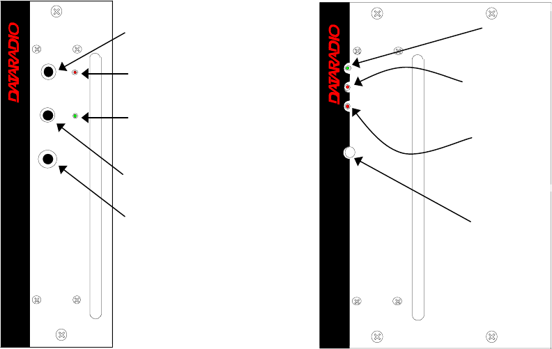
3.2.1.5.1 Radio Network Indicators
The Radio Network LEDs are useful when trou-
bleshooting as an indication of network activity.
It can help isolate transmission problems.
Figure 12 - RF indicators
CS Carrier Sense - Steady light indicates that an
incoming radio data signal is being detected by
the DSP modem. CS signal is not user-adjustable.
RX Receive Data – Flashing light indicates unit is
internally receiving data from the radio network.
TX Transmitter ON – blinks green indicates
(depending on display mode selected):
• That a data packet or ACK (packet acknowl-
edgment) is being transmitted.
• That an idle packet, data packet or ACK is
being sent. Test transmission display is done
in red.
CS RX TX
RF
120 20170-302 ParagonPD Technical Manual
16
3.2.1.5.2 RS-232 Port Indicators
The RS-232 LEDs normally indicate port activity
on the port selected. See section 3.2.1.4 above for
instructions for selecting display mode.
Figure 13 - RS-232 Port LED indicators
CM Command Mode - LED lights and re-
mains lit while the selected port is ac-
cessing the Command Processor. It lights
ON and OFF while being configured.
FR Flow Control on Receive - the BDLCPD
has received a flow control signal from
the device connected to it. When it lights,
BDLCPD has stopped sending data to the
DTE. When LED goes out, the port ter-
minal is again ready to receive data.
FT Flow Control on Transmit - the BDLCPD
has sent a flow control signal to the DTE
asking it to stop sending data. The LED
remains lit as long as the terminal is be-
ing held off.
RD Receive Data - when lit, it shows that the
Receive Data pin 3 on the RS-232 inter-
face connector is active. Since all
BDLCPD are configured as DCE, it means
that the DTE is receiving data from the
BDLCPD.
TD Transmit Data - shows the status of
Transmit Data pin 2 of the RS-232 inter-
face. When lit, the DTE is sending data
to the BDLCPD.
3.2.1.5.3 Check and Power LEDs
CK Check:
Normally flashing rapidly (about 6 cps),
indicates microprocessors are working
correctly and power is applied.
Not flashing indicates unit is not
functioning.
Blinking slowly (1 cps), indicates the pa-
rameters contents of the flash memory have
been corrupted. The unit automatically loads
its set of factory default parameters and
starts beeping at 20 seconds intervals.
May also indicate DSP-modem re-
initialization has occurred
3.2.1.5.4 Alarm Indicators
All alarm conditions will cause the BDLCPD to
light one or more of the LED indicators. LEDs
remain ON when lit until cleared by either
pressing PF 1 (without affecting operation of the
unit) or RESET (cycling unit OFF and ON).
Figure 14 - ALARMS LED indicators
LM Local Minor Alarm - when lit, indicates
the presence of any of the following mi-
nor faults:
- Parity, framing or overrun error at any
RS-232 port.
- Out of buffers. No memory available to
accept data from a local terminal device.
Usually denotes a flow control problem.
- Flash memory error. At power-up or
reset, the unit detected a change in non-
volatile memory.
RM Remote Minor Alarm - when lit, indi-
cates any of the Local Minor Alarm
listed above have taken place at the re-
mote end of the link (i.e. the mobile the
local base station is currently communi-
cating with). It will also light when a
protocol error has been detected on the
network.
In a network using the “Host Link Ac-
tive” (MSC) feature, the RM LED,
flashing in-sync with the CK LED, indi-
cates that the link is down.
LF Link Failure - when lit, indicates that the
base station fails to receive an ACK for a
321
RS-232
CM FR FT RD TD
ALARMS
LM RM LF UF
120 20170-302 ParagonPD Technical Manual
1
7
packet sent and for all subsequent retries.
Some data has possibly been lost. LF is
not functional if all active ports are set to
NAR mode.
Link fails are inevitable during normal
operation (mobiles temporarily out of
range, in a tunnel, parked in a dead spot,
etc.). A lit LF LED is not normally cause
for concern.
UF Unit Failure - when lit, the unit requires
attention:
- The BDLCPD is not operable;
It may indicate detection of a system
software error trap.
- The BDLCPD is operable;
Indicates that on power-up, invalid data
was detected in the serial EEPROM chip
(located in the radio modules). It may
also indicate that connection to the radio
modules is incorrect or that radio power
is not applied.
The LM, RM and UF alarms also sound a beep
when a fault occurs. The LF alarm is silent.
3.2.2 BDLCPD Rear panel
Referring to Figure 4, the rear panel of the
BDLCPD has the following set of chassis con-
nectors:
• One DB-25F connector
– DEV1 - Connects to user’s application.
a) DMP 19200 or 38400 baud for single-
site installations
b) MSCP 19200 or 38400 baud for multi-
site installations
• Four DE-9F connectors:
– DEV2 - usually connected to Dataradio’s
WinRIS program (Dedicated or DMP at
19200 baud).
– DEV3 - Dedicated (up-to 9600 baud)
– DEV4 and DEV5 - not used
• One DA-15M connector:
– DEV6 Digital I/O - not used
• One DB-25M connector:
– EXT RADIO/TEST - connects to the Ra-
dio assembly through the radio interface
cable (see Figure 15)
3.2.2.1 RS-232 Signal Levels
In the description of data signals in Table 7, the
following conventions are used:
Table 5 - RS-232 Signal levels
Term Alternates Signal level
ON Asserted, spacing +3 to +15 V
OFF Dropped, marking -3 to -15 V
3.2.2.2 Pin Functions
Table 6 - DTE Port 9-pin funtions
DE-9 F
pin # Function (RS-232 signal levels)
1 DCD – from ParagonPD, normally asserted
2 RXD – data from ParagonPD
3 TXD – data to ParagonPD
4 DTR – to ParagonPD, handshaking
5 Ground
6 DSR – from ParagonPD, tied to VCC through
current limiting resistor
7 RTS - to ParagonPD, handshaking
8 CTS – from ParagonPD, handshaking
9 Reserved
Table 7 - DTE Port 25-pin functions
DB-25F
pin # Function (RS-232 signal levels)
1 and 7 Ground
2TXD – data to BDLCPD
3RXD – data from BDLCPD
4RTS – to BDLCPD, must be asserted
5CTS – from BDLCPD, handshaking
6DSR – from BDLCPD, always +8V
8DCD – from BDLCPD, always asserted
9RI - from BDLCPD, always –8V
20 DTR – to BDLCPD, handshaking
We recommend the use of shielded 9-wire or
25-wire cables with all pins connected.
Dataradio recommends the use of secure (i.e.
password protected and/or dial-back) modems in
any installation where dialup access is provided.
.
120 20170-302 ParagonPD Technical Manual
18
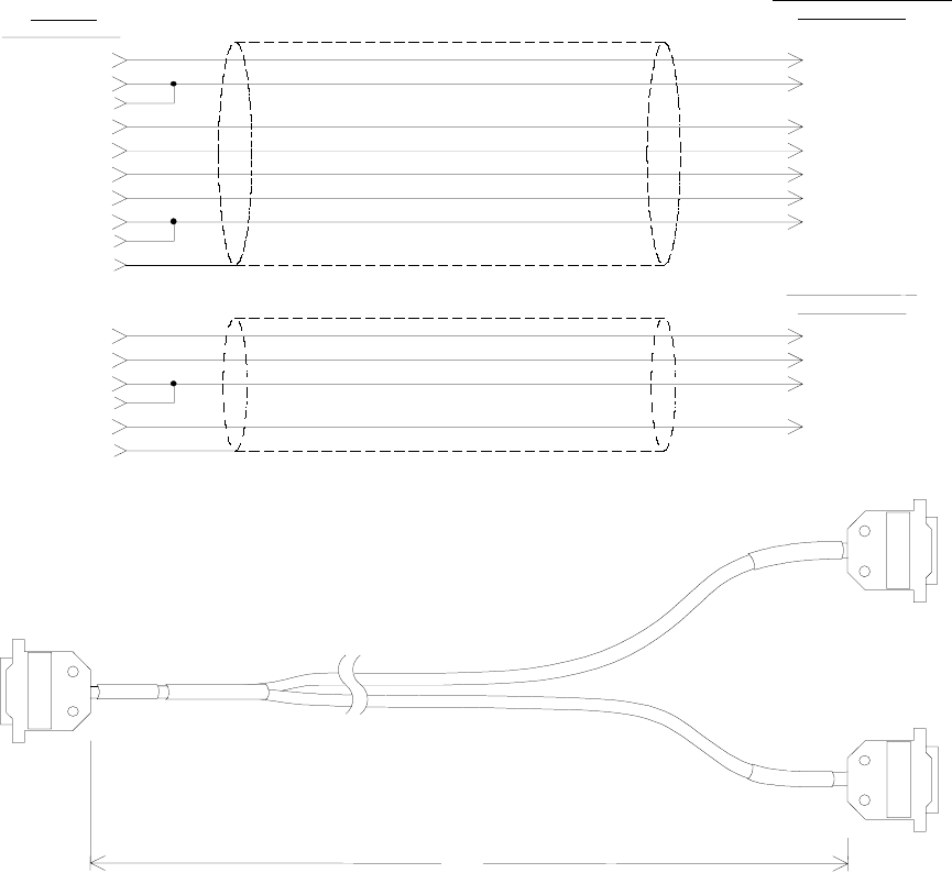
Figure 15 - BDLCPD Y cable and pinout
DB-25 FEMALE (PL1)
BACKPLANE 1 / RX 1 & EXCITER
BDLC D212
18TXA TXA (from SK3 pin 8)11
1RX1 EEPROM (from SK1 pin
1
EXTIO_OUT1
3RXA (1) RX AUDIO 1 (from SK1 pin 6)
24
9 RX RSSI (from SK1 pin 5)
RSSI (1) 16
6
PTT 15
SHI ELD
YELLOW
GRAY
GREEN
BLUE
ORANGE
17
SHIELD
RXA (2) RX AUDIO 1 (from SK1 pin 6)
24
9 RX RSSI (from SK1 pin 5)
RSSI (2)
2
GROUND (2) 13
SHI ELD
BROWN
VIOLET
RED
15
SHIELD
DB-25 FEMALE (P8)
EXTIO_IN1
10
22
GROUND (1) 4BLACK
EXTIO_OUT3 7WHITE
EXTIO_IN3 24
TX KEY (from SK3 pin 13)
13 GROUND
TX EEPROM (from SK3 pin 1
)
5
1
14
9EXTIO_OUT2
EXTIO_IN2 23
1 RX 2 EEPROM (from SK1 pin
GROUND
DB-25 FEMALE (PL1)
BACKPLANE 2 / RX 2
BLACK
18.00"
730-03374-102
L
E
F
T
(
R
X
1
-
E
x
)
R
I
G
H
T
(
R
X
2
)
TO BDLC
1)
1)
)

120 20170-302 ParagonPD Technical Manual
19
4. Trouble-Shooting and Test-
ing
The checks described below should be done at
time of installation, annual intervals or when-
ever deterioration in performance is noted.
4.1 Equipment Required
• In-line watt meter (150W & 10 W ranges)
• Radio service monitor (IFR-120B with
option 03: 30KHz IF filter or equivalent).
• RG-214 or RG-223 cable with N-Type male
connector to connect ParagonPD to the serv-
ice monitor.
• WinRIS 3.11 or later1
Important note: Before proceeding make sure
that the service monitor has been calibrated
recently and has warmed up for at least the
time specified by its manufacturer.
Some reported frequency and deviation prob-
lems have actually been erroneous indications
from service monitors that have not adequately
warmed up. This is particularly likely when field
service is done during winter months.
1 To learn how to launch the Windows-based
software alignment and system-testing tool
WinRIS, please refer to the readme.txt file on
the application’s installation diskette.
For functional details of the numerous buttons
and menu-selectable items available, please
refer to the program’s context sensitive help.
It is also possible to access the help informa-
tion via the F1 key.
4.2 Recommended Checks
A) After an installation
1. LED Indications
2. Using WinRIS, Save “unit config” to a
file
3. Transmitter Output Power
4. Transmitter Reflected Power
5. RF Link test between Paragon
PD and
mobile unit(s)
B) For annual maintenance & trouble-
shooting
Same checks as A) plus:
6. Carrier Frequency Error
7. TX Deviation
8. Low Frequency Balance
9. 12 dB SINAD
10. Receiver distortion
11. RSSI check
Transmissions for some of the tests above can
be initiated by pressing the PF1 membrane but-
ton located on the front of the BDLCPD. For de-
tails on its use, refer to Table 3 and section
3.2.1.3 on page 14.

120 20170-302 ParagonPD Technical Manual
20
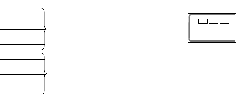
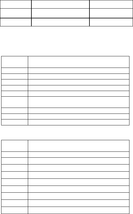
Table 8 - Checklist A (after installation)
CHECKLIST A
(ParagonPD)
Recommended Check out after Installation
Step ACTION EXPECTED RESULTS
at 25°
°°
°CMEASURE WITH IF NOT?
1Normal Power-up
Sequence BDLCPD beeps once, all LEDs come ON for about four seconds, the green
LEDs then flash in a “ripple” pattern for close to two seconds. All LEDs go OFF
except the CK that should flash 6 to 8 times per second. For functions, see
section 3.2.1.5
2Connect and save unit
config
Press WinRIS Get but-
ton
as per WinRIS Help content
3Transmitter Output
Power
Press TXON (Unmod)
VHF/UHF: 20 - 100 watts
800 MHz: 20 - 70 watts
900 MHz: 65 - 100 watts
+10%, -10%
Service monitor set
to read power
or
150W in-line watt-
meter installed as
close as possible to
the unit antenna
connector.
1Check for bad connec-
tions, damaged coax cable,
etc.
4Transmitter Reflected
Power
Press TXON (Unmod)
< 5% of forward power or
as specified by System
Engineering.
10W in-line watt-
meter Check for bad connections,
damaged coax cable, etc.
5RF Link test
Use the mobile address
function and “Send” but-
ton to dynamically test
the link
Look for
“Delivery confirmed” on
the Status bar
Refer to 4.3.1 and to
WinRIS Help
content.
Mobile is out of range
Refer to factory technical
support.
1 (unless unit has been set a lower value). Note that readings less than 100 watts for VHF/UHF or 70 watts for 800 MHz models,
may be due to losses in cables used for testing. Check also your wattmeter frequency calibration curve. Do not be too ready to
condemn the transmitter or the RF feedline & antenna installation.

120 20170-302 ParagonPD Technical Manual
21
Table 9 - Checklist B (General)
CHECKLIST B (ParagonPD)
General Check out (part1 of 2)
ParagonPD units are set and characterized at the factory to optimize performances.
It is not recommended to try readjusting units unless it is really required.
Misadjusting a unit may result in significant performance losses.
The proposed adjustments in the "IF NOT?" column below, should be tried ONLY if system data
performance degradation is noticed combined with out-of-tolerance items.
Step ACTION Expected Results at 25°
°°
°CMEASURE WITH IF NOT?
1Normal Power-up
Sequence BDLCPD beeps once, all LEDs come ON for about four seconds, the green LEDs
then flash in a “ripple” pattern for close to two seconds. All LEDs go OFF except the
CK that should flash 6 to 8 times per second. For functions, see section 3.2.1.5
2Connect and save
unit config
Press WinRIS Get
button
as per WinRIS Help content
3
Transmitter Output
Power
Press TX ON (Unmod)
VHF/UHF: 20 - 100 watts
800 MHz: 20 - 70 watts
900 MHz: 65 - 100 watts
+10%, -10%
Service monitor set
to read power
or
150W in-line watt-
meter installed as
close as possible
to the unit antenna
connector.
Adjust “Power” on the front
panel of the “Power Amp”
( see Figure 8)
4Transmitter
Reflected Power
Press TXON (Unmod)
< 5% of forward power or
as specified by System
Engineering.
10 W in-line
wattmeter Check for bad connections,
damaged coax cable, etc.
5Carrier Frequency
Error
Press TX (Unmod)
< ±300 Hz Service monitor set
to read frequency
error
Adjust TCXO (IC700)
(see inside Exciter module at,
Figure 28 (800), Figure 30
(UHF), Figure 32 (VHF) )
6TX Deviation (KHz)
Press
TX (Unmod)
Carrier will be modu-
lated with a 1 kHz tone.
Refer to "Figure 16 - Carrier
deviations for Tone or Data
Modulation" per bit rates
Tolerance is +5%, -10%
for all bit rates.
Service monitor set
to read deviation.
(IF filter set to Mid
or 30 kHz position) Adjust according to Appendix 1
- ParagonPD Deviation adjust
on page 44
7Low Frequency
Balance
Initiate a
TX Random data
test
via BDLCPD’s PF1
(See Table 3)
a) Record deviation level
read from step 6
b) Record deviation read
from TX Random test
c) Difference between
a) and b) should be:
< 600 Hz (DGMSK)
< 1.5 kHz (xSR4FSK, HC)
< 2.0 kHz (xSR4FSK,
FC/NPSPAC)
Service monitor set
to read deviation
(IF filter set to Mid
or 30 kHz position,
all audio filtering
disabled )
Refer to
Section 5.2.3.4

120 20170-302 ParagonPD Technical Manual
22
CHECKLIST B (ParagonPD)
General Check out (part2 of 2)
ParagonPD units are set and characterized at the factory to optimize performances.
It is not recommended to try readjusting units unless it is really required.
Misadjusting unit may result in significant performance losses.
The proposed adjustments in the "IF NOT?" column below, should be tried ONLY if system data
performance degradation is noticed combined with out of tolerance items.
Step ACTION EXPECTED RESULTS at
25°
°°
°CMEASURE WITH IF NOT?
Set the service monitor to generate on the selected receive frequency. Verify alternately for both receivers.
The carrier should be modulated with a 1.0 kHz tone at deviation level specified below:
812 dB SINAD
(Dataradio wide band
measurement
method: no audio
filtering)
- For Full channel
unit, set deviation
to ±3 kHz.
- For Half &
NPSPAC channel
unit, set deviation
to ±1.5 kHz
Better than -108 dBm
including cable loss
(Typically -109 to -110 dBm)
- Backplane correspond-
ing to the receiver being
verified: SK1, Pin 6 (see
Figure 24)
- Service monitor (IFR)
set to SINAD
- IFR IF filter set to MID
position or 30 kHz wide
filter.
Refer to section 5.2.2
9Receiver distortion
(Dataradio wide band
measurement
method: no audio
filtering)
- Set service monitor
RF Gen output to –
70 dBm
- Deviation level as
per SINAD above.
≤ 5.5 %
(Typically < 3.5 %)
- Backplane correspond-
ing to the receiver being
verified: SK1, Pin 6 (see
Figure 24)
- Service monitor (IFR)
set to SINAD
- IFR IF filter set to
MID position or 30
kHz wide filter.
Refer to section 5.2.2
10 RSSI
Apply to each
receiver input the
following RF level
UHF & 800/900Mhz:
-110dBm
VHF: -100 dBm
UHF & 800 MHz:
2.0 VDC (+/- 0.3VDC)
VHF:
4.0 VDC (+/- 0.35VDC)
Note: BDLC must be
connected to the
radio during the
measurements
- Backplane correspond-
ing to the receiver being
verified: SK1, Pin 5 (see
Figure 24)
- DC Voltmeter
measurement
Refer to section 5.2.2.5
for all models.
Refer to factory
technical support only if
RX data performance
degradation is noticed
combined with out of
tolerance RSSI
readings.
120 20170-302 ParagonPD Technical Manual
23
4.3 Additional test details
4.3.1 RF Data Link Test
A link test between a mobile and a known base
station can be done using the WinRIS "Address"
and "Send" functions. The “Address” and “De-
vice” fields, the “Send” button and the “Chat”
message screen are used to send messages to
specific mobile or base or to carry out RF test.
Start by entering the address of the mobile (or
base station) you wish to send a test message to
or test:
1- Specify the address:
Addresses may be entered by typing directly in
the “Address” field in two ways:
- Numerically, the valid address range is
1-126.
- As an “Alpha-Mapped-Nibble” (AMN)
address, consisting of upper case letters
in the range A-P.
The valid address range is A to GN.
- The base address is usually: 1.
- The program may display one of the
following messages on the status bar:
- For ParagonPD products:
“address is not in AMN or number for-
mat”
- For mobile products:
“address is not in the range A – GN”
In either case, check that the address entered
is within the acceptable range, is of a valid
format and correctly typed.
2- Enter the Device number for mobile (or base
station).
3- Press the Send button.
The Chat window reports “Sent to xx mo-
bile” (where xx is mobile name).
If test is successful:
Status line reports “Delivery confirmed.
If test unsuccessful:
Chat window reports “Waiting”,
Then the Status line reports “Delivery
Failed”.
4.3.2 Carrier deviations
Carrier Modulation
Tone Data
Network Speed
(b/s)
Typical deviation in
kHz
(1000Hz test tone)
Maximum
deviation
in kHz
Full Channel (800MHz)
32000 ± 3.6 ± 5.6*
xRC4FSK
25600 ± 3.7 ± 5.7 *
Full Channel (UHF/VHF)
32000 ± 4.3 ± 6.3*
xRC4FSK
25600 ± 4.0 ± 6.0*
Full Channel (VHF/UHF & 800MHz)
19200 ± 4.0 ± 4.6
DGMSK
9600 ± 3.0 ± 3.6
NPSPAC Channel (800MHz - U.S. only)
8000 ± 2.5 ± 3.1
DGMSK
9600 ± 2.5 ± 3.1
16000 ± 2.4 ± 3.9
xRC4FSK
19200 ± 2.1 ± 3.6
900MHz Channel ( U.S. only)
8000 ± 2.8 ± 3.4
DGMSK
9600 ± 3.2 ± 3.9
16000 ± 2.4 ± 3.9
xRC4FSK
19200 ± 2.4 ± 3.8
Half-Channel (VHF/UHF & 800MHz)
8000 ± 1.5 ± 2.1
DGMSK
9600 ± 2.5 ± 3.1
14400 ± 2.0 ± 3.6
xRC4FSK
16000 ± 1.6 ± 3.2
* Deviation shown may seem higher than normal, however
they fall within the following appropriate FCC’s masks limits.
Figure 16 - Carrier deviations for Tone or Data Modulation
120 20170-302 ParagonPD Technical Manual
24
5. Radio Programming and Adjustments
All receiver procedures detailed in this section should be done twice: once for the “Main” (or RX1) re-
ceiver module and a second time for the “Auxiliary” (or RX2) receiver module. Connect to the relevant
module and its corresponding backplane PCB as required.
5.1 Series II Radio Programming
This procedure describes the steps needed to pro-
gram the ParagonPD base station UHF, VHF &
800MHz radios (half & full channels).
5.1.1 Recommended Items
- 486 PC or better, MS-Windows 3.1 © or later
- T800win programming kit for Series II:
- PGM800Win programming software user's
manual
- PGM800Win Windows based programming
software
- T800-01-0002 programming cable (DB-25 to
RJ-45 cable)
- Standard 25-pin parallel cable (terminated
Male/Female)
5.1.2 Module Programming
Before starting programming, have a PC running
MS-Windows © and the Tait PGM800Win soft-
ware for Series II Base station.
This program supports the use of a mouse but may
be used without one if required. Keyboard access
follows the conventional MS-Windows © method
as briefly described below:
- Press and hold the “Alt” key while pressing at
the same time the relevant hotkey as indicated
by an underlined letter on the menu command.
- On a drop-down menu, press only the hotkey
without pressing the “Alt” key.
- Use the “Tab” key to cycle available fields
and the “Enter” key to validate entries. E.g.
Pressing “Alt”+F opens the File drop-down
menu and pressing “A” opens the Save As di-
rectory service box.
Receiver VCO and front-end alignment will be
required when new receiver frequency is pro-
grammed outside the radio tuning range:
800/900 = ± 3.0 MHz from previous center
frequency
UHF = ± 2.5 MHz from previous center
frequency.
VHF = ± 1.5 MHz from previous center
frequency.
Exciter and PA alignment will be required when
new transmitter frequency is programmed outside
the radio tuning range: ± 4 MHz from previous
center frequency.
1. Connect the PC, via the supplied program-
ming lead, to the speaker panel’s front-
mounted RJ11 connector.
2. Run Tait PGM800Win program and follow
instructions found in the T800 Programming
Software User’s Manual to select the proper
module to be programmed.
3. Program required channel's frequencies.
– Do not program any CTCSS tones on
channels.
– Do not change any other parameters.
– Refer to Figure 17, Figure 18, Figure 19
and Figure 20 for screen program
examples.
4. Save the base station programming info to a
file for further reference.
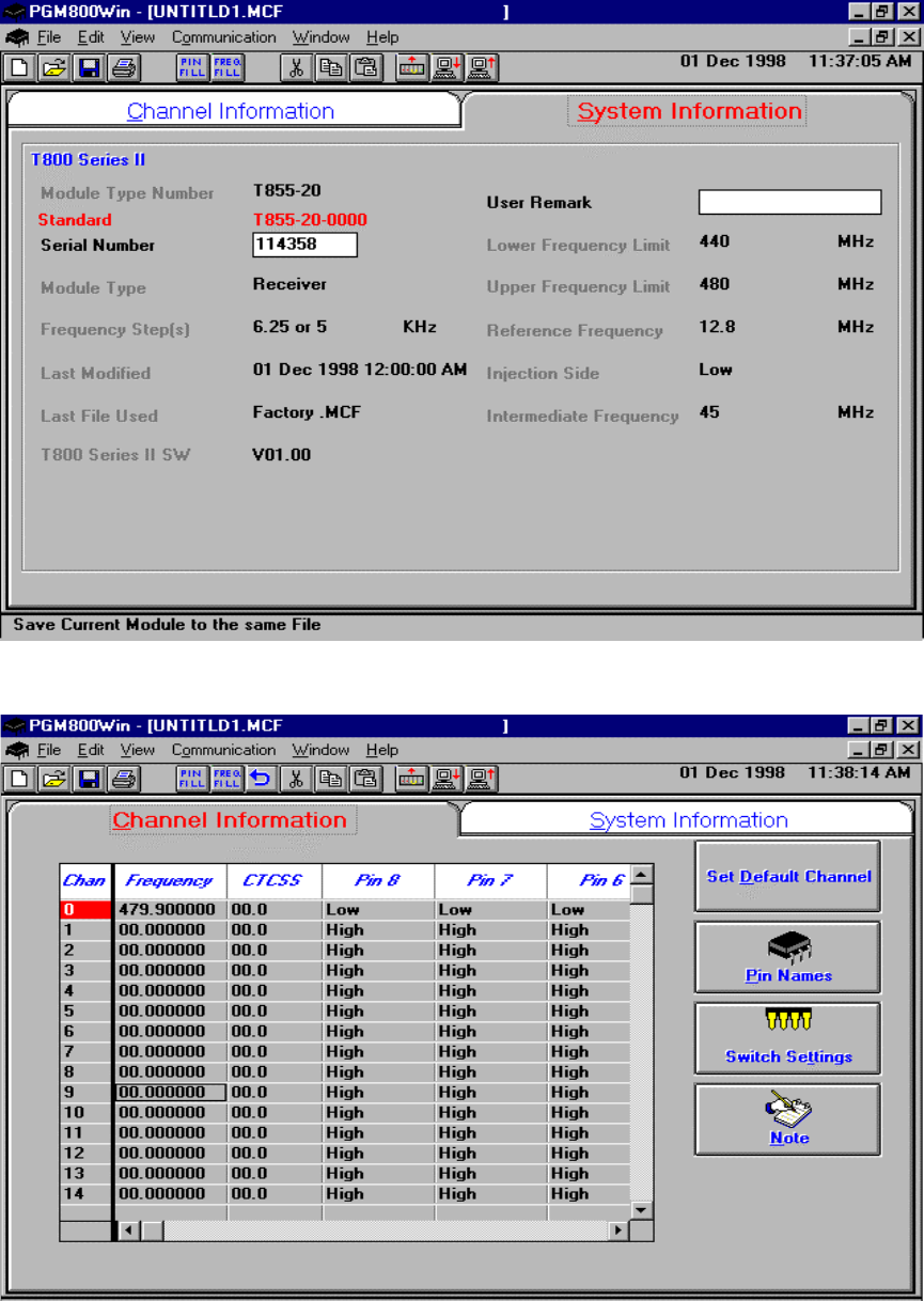
120 20170-302 ParagonPD Technical Manual
25
Figure 17 - Receiver System Information
Figure 18 - Receiver Channel Information screen
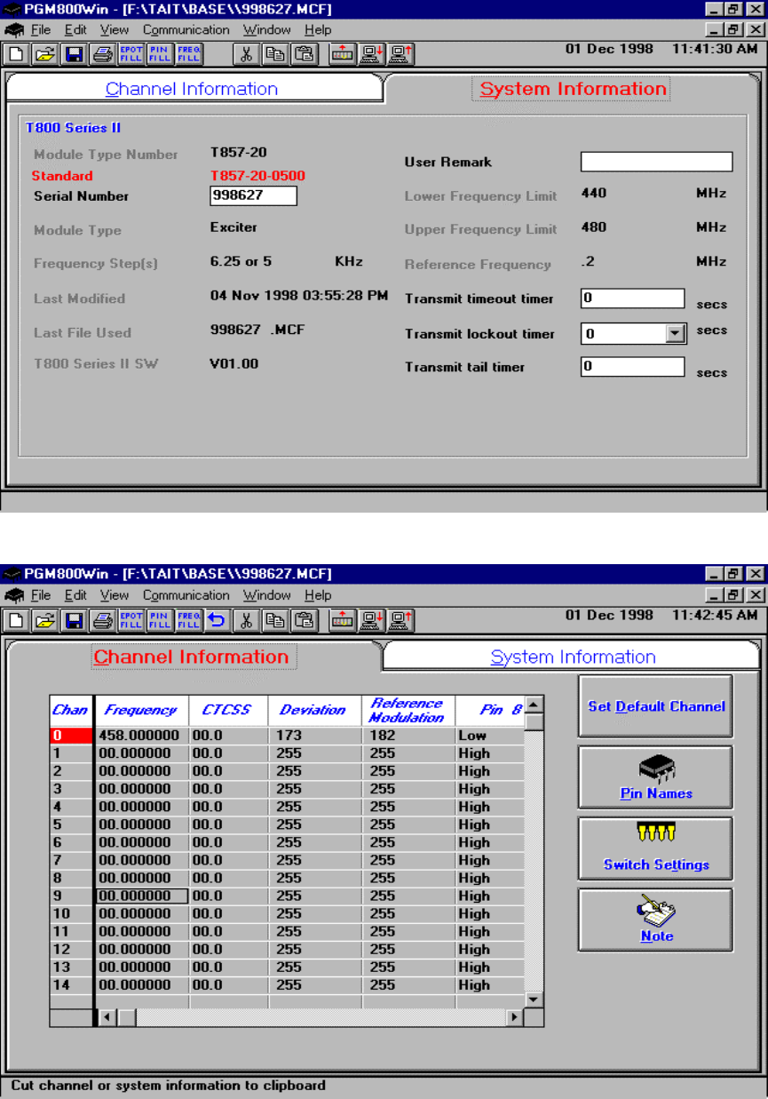
120 20170-302 ParagonPD Technical Manual
26
Figure 19 - Exciter System Information screen
Figure 20 - Exciter Channel Information screen
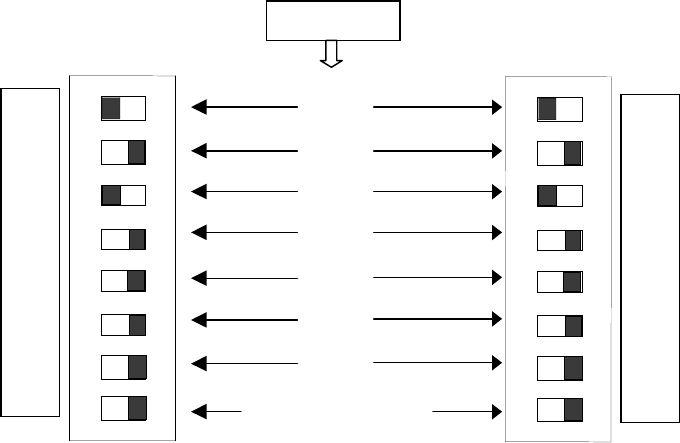
120 20170-302 ParagonPD Technical Manual
27
5.1.3 Channel Selection via DIP
Switches
The backplane-mounted DIP switch settings
override the default channel programmed by
PGM800Win.
To set a default channel via the software, all
DIP switches must be set to “OFF” (i.e.
00000000).
When a switch is “Off”, its binary count is ac-
tive; when a switch is “ON” its binary count is
inactive. The various DIP switch combinations
of ON or OFF make up a binary total, which
identifies the channel number.
To select a channel, set the appropriate DIP
switch or switches to “OFF” to make the binary
count total the channel number you want. Set all
other switches to “ON”.
It is recommended to set both SW1 (RX) and
SW2 (TX) to the same settings on both back
plane boards.
Example: To select channel 5, set the DIP
switches as shown below:
Figure 21 - Backplane DIP switches example - Channel 5 selected
Binary Value
1
2
4
8
16
32
64
Always ON except when
default channel is required
CHANNEL SWITCH TX
CHANNEL SWITCH RX
1
2
3
4
5
6
7
8
O
F
F
1
2
3
4
5
6
7
8
O
F
F

120 20170-302 ParagonPD Technical Manual
28
5.2 Series II Radio Tuning
This section covers some basic Series II base station modules radio tuning and verification for:
- VHF (T83x-xx-0200),
- UHF (T85x-xx-0250) and
- 800 MHz/900 MHz (T88x-xx-0200).
Note: Usually, this section is not done unless called for in section 5.1 “Series II - Radio Programming”
or in Table 9 “Checklist B” (General).
To identify the radio modules, check the part number on the manufacturer’s label at the back of the
Receiver, Exciter and Power Amplifier modules:
RX TX PA
T885-10-0200 (800-870 MHz, 25kHz)
T885-15-0200 (800-870 MHz, 12.5kHz
& NPSPAC)
T885-30-0200 (890-960 MHz, 25kHz)
T885-35-0200 (890-960 MHz, 12.5kHz)
T881-1x-0200 (800-870 MHz)
T881-1x-0200 (800-870 MHz)
T881-3x-0200 (890-960 MHz)
T881-3x-0200 (890-960 MHz)
T889-10 (850-870 MHz)
TPL- PA8-2BF-LMS (890-960)
T855-10-0250 (400 - 440 MHz, 25kHz)
T855-15-0250 (400 - 440 MHz, 12.5kHz)
T855-20-0250 (440 - 480 MHz, 25kHz)
T855-25-0250 (440 - 480 MHz, 12.5kHz)
T855-30-0250 (480 - 530 MHz, 25kHz)
T855-35-0250 (480 - 530 MHz, 12.5kHz)
T857-1x-0250 (400 - 440 MHz)
T857-2x-0250 (440 - 480 MHz)
T857-3x-0250 (480 - 520 MHz)
T859-10-0000 (400 - 440 MHz)
T859-20-0000 (440 - 480 MHz)
T859-30-0000 (480 -520 MHz)
T835-10-0200 (136 - 156 MHz, 25kHz)
T835-15-0200 (136 - 156 MHz, 12.5kHz)
T835-20-0200 (148 - 174 MHz, 25kHz)
T835-25-0200 (148 - 174 MHz, 12.5kHz)
T837-1x-0200 (136 - 156 MHz)
T837-2x-0200 (148 - 174 MHz)
T839-10-0000 (136 - 156 MHz)
T839-20-0000 (148 - 174 MHz)
5.2.1 Test Equipment
- Digital Multimeter & probes (e.g. Fluke 77)
- 1 HP 34330A Shunt 30A (UHF only, used for transmitter current measurement)
- Digital or Analog calibrated Oscilloscope & scope probes (X1, X10 selectable)
- Calibrated COM-120B (.001ppm OCXO and 30kHz IF options)
- 3-foot length of double-shielded N-M to BNC-M cable (RG-214 or RG-223)
- 2x 'BNC' to 'N' type adapters (e.g. Amphenol, Greenpar).
- Bird RF power meter with 150W / 50 ohm dummy load (optional)
- 3dB 150–watt attenuator
- 1x Torx screwdriver #T-10 and #T-20
- Pozidriv screwdriver #1 & #2
- 1x Six-inch adjustable wrench
- RF tuning/trimming tools.
- Extender Rail Kit for Series II chassis (T800-13-0000)
- 1x 6" coax cable N-M to BNC-M (comes with the radio to connect the exciter to the PA)

120 20170-302 ParagonPD Technical Manual
29
5.2.2 Receiver module (T885-xx-0200, T855-xx-0250 & T835-xx-0200)
Note 1: Refer to Figure 27 (T885), Figure 29 (T855) and to Figure 31 (T835) for locating tuning
controls.
Note 2: When the synthesizer is unlocked, the front panel green LED called "Supply" will flash
indicating that it needs re-tuning.
Warning,
The LED will also flash when the unit is in setup mode while connected to the PGM800win
program.
5.2.2.1 Initial Setup
This initial setup will be used during all receiver alignment procedures described below:
1. Remove the receiver (T885, T855 or T835) module from the ParagonPD rack frame
2. Remove the receiver top cover (nearest the handle).
3. Connect the ParagonPD Extender Rail Kit for Series II to the empty chassis receiver slot.
4. Prepare the Multimeter to DC Volts.
5. Apply power to the ParagonPD.
5.2.2.2 Synthesizer Alignment
Single channel: Connect the Multimeter to either side of L504 (T885) or the long lead of L1 (T855
and T835) in the VCO (this measures the synthesizer loop voltage).
1. T885 (800/900 MHz) Tune VCO trimmer CV500 for a synthesizer loop voltage of 10VDC.
2. T855 (UHF) Tune VCO trimmer C6 for a synthesizer loop voltage of 10V DC.
3. T835 (VHF). Tune VCO trimmer CV1 for a synthesizer loop voltage of 9VDC.
Multiple channels (adjusting as shown for single channel above):
1. T885 (800/900 MHz) Adjust the VCO loop to 10V using the middle frequency channel.
2. T855 (UHF) Adjust the VCO loop to 10V using the middle frequency channel.
3. T835 (VHF) Adjust the VCO loop to 9V using the middle frequency channel.
4. All channels should lie within the upper and lower limits of respectively
All channels should lie within the upper and lower limits of 16V and 3V respectively for
the T885 and T855 or within 13V and 5V for the T835.

120 20170-302 ParagonPD Technical Manual
30
5.2.2.3 Front-End Alignment
1. IFR COM120B settings:
a) Connect a 3 feet long double shielded cable (N-M to BNC-M) between the IFR T/R output and the
receiver antenna connector.
b) Select the generator mode (GEN button) and set to the main receiver channel frequency
c) Select and turnon GEN2
d) Set the FM Deviation to ±3kHz (full channel) or ±1.5kHz (half channel) using 1KHz sine
e) Select SINAD meter
f) Use a X1 scope probe connected to SINAD input and monitor the Discriminator O/P on the back-
plane at SK1 pin 6 (RX-audio1). Alternately, it is also possible to monitor at the receiver I/O Pad
P207 (T885), the receiver TP314 (T855) or at the receiver IC350 pin 7 (T835).
2. Adjust the helical resonators for best SINAD: #H400, #H401 and #H900 (T885); #FL410 and #FL420
(T855) or L410, L420, L460 and L470 (T835).
3. Continually decrease the RF level to reach 12dB SINAD, then re-do step 2) & 3) again. The absolute
minimum requirement level to reach is -108dBm (typical level is -109 to -110 dBm)
4. Perform the SINAD linearity tests described in paragraph 5.2.2.4. If it fails to pass the requirement,
contact your Dataradio technical support.
WARNING: Do NOT attempt to re-tune the IF stages
(I.e. L300 and L301 for T885, L310 to L390 for T855 or L330 to L360 and
CV318 for T835).
These adjustments do not need to be re-adjusted after frequency re-programming. Touch-
ing these coils will have a direct impact on the modem DSP ISI coefficient settings and may
reduce significantly the radio performances over data.
5.2.2.4 SINAD and Linearity Check
1. Apply the following settings to the IFR COM-120:
a) Generator mode, Output T/R, TX frequency to match the main radio RX frequency
b) Filter set to wide band (no audio filter)
c) Select Gen2 (Modulating tone fixed to 1KHz). All other Gen must be off.
d) Set deviation to ±3.0KHz for full channel or ±1.5KHz for half channel radios.
e) Use a X1 scope probe connected to the IFR SINAD input and monitor the Discriminator O/P on the
radio backplane at SK1 pin 6 (RX-audio1). Alternately, it is also possible to monitor at the receiver
I/O Pad P207 (T885), the receiver TP314 (T855) or at the receiver IC350 pin 7 (T835).
2. Lower the RF level to get a 12dB SINAD reading. Level should be better than -108dBm (including ca-
ble loss).
3. Offset the IFR TX frequency 2kHz (full channel) or 1kHz (half / NPSPAC channel) above the main
radio RX frequency, record the SINAD reading. It should remain within 1.5 dB from the on frequency
SINAD reading. For T885 and T855, use above values, for T835 use 1.5kHz (full channel) or 0.8kHz
(half channel).
4. Offset the IFR TX frequency 2KHz (full channel) or 1kHz (half / NPSPAC channel) below the main
radio RX frequency, record the SINAD reading. It should remain within 1.5 dB from the on-frequency
SINAD reading. For T885 and T855, use above values, for T835 use 1.5kHz (full channel) or 0.8kHz
(half channel).
Note: If one of the above requirements is not met, try to re-tune the front-end. If still failed, contact
your Dataradio technical support.
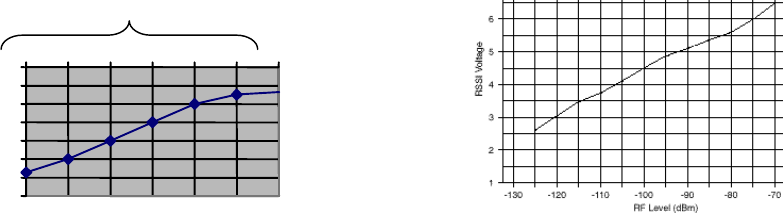
120 20170-302 ParagonPD Technical Manual
31
5.2.2.5 RSSI Adjustment
- Caution: mis-adjusting RSSI may reduce the ParagonPD's Parallel Decode (PD) performance.
- BDLCPD must be connected to the radio backplane during this process.
1. T885-xx-0200 (800/900 MHz) and T855-xx-0250 (UHF) receivers:
- Apply an on-channel signal from the RF generator at a level of -110 dBm modulated by a 1 kHz tone at
a deviation of ±3kHz (full channel) or ±1.5kHz (half / NPSPAC channel).
- Adjust RV 345 (RSSI level) for T885, RV320 (RSSI level) for T855 to give 2.0V RSSI output at
SK330 pin 2 (T855) or on backplane SK1 pin 5 when measured with a voltmeter (See Figure 24 for test
point location).
2. T835-xx-0200 (VHF) receivers:
- Apply an on-channel signal from the RF generator at a level of -100 dBm with deviation of ±3kHz
(full channel) or ±1.5kHz (half channel) at 1kHz tone.
- Adjust RV320 (RSSI level) to give 4.5V RSSI output at RSSI test point (near quad. Coil L360) or on
backplane SK1 pin 5 when measured with a voltmeter (Figure 24 - T800-50-0001) for test point loca-
tion).
The following RSSI graphics are given as general information only.
Refer to factory technical support only if RX data performance degradation is noticed combined with
something that does not look like those RSSI curves.
Figure 22 - T855 and T885, Typical RSSI Curve: volt to dBm Figure 23 - T835, Typical RSSI Curve: volt to dBm
0
1
2
3
4
5
6
7
-120 -110 -100 -90 -80 -70
dBm
Voltage
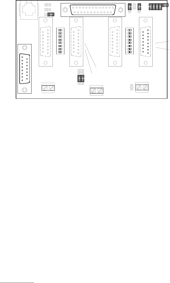
120 20170-302 ParagonPD Technical Manual
32
Figure 24 - T800-50-0001 Backplane
5.2.3 Exciter Module (T881-xx-0200,T857-xx-0250 or T837-xx-0200)
Note 1: Refer to Figure 28 (T881), Figure 30 (T857) and to Figure 32 (T837) for locating tuning
controls and components.
Note 2: When the synthesizer is unlocked, the front panel green LED called "Supply" will flash indi-
cating that it needs re-tuning.
Warning:
The LED will also flash when the unit is in setup mode while connected to the PGM800win program.
5.2.3.1 Initial Setup
1. Shut down power to the base station.
2. Prepare the Multimeter to DC Volts.
3. Remove the exciter (T881, T857 or T837) module from the base station rack frame.
4. Remove the exciter top cover (nearest the handle).
5. Connect a 3 feet long double shielded cable (N-M to BNC-M) between the IFR T/R output and
the exciter antenna connector.
6. Connect the ParagonPD Extender Rail Kit to the empty chassis exciter slot.
7. Apply power to the base station.
5.2.3.2 Synthesizer Alignment
Single channel: Connect the Multimeter to either side of L309 (T881) or the long lead of L1 in the
VCO (T857 and T835) (this measures the synthesizer loop voltage).
1. T881 (800/900 MHz) Tune VCO trimmer CV300 for a synthesizer loop voltage of 10V DC.
2. T857 (UHF) Tune VCO trimmer C6 for a synthesizer loop voltage of 10V DC.
3. T837 (VHF). Tune VCO trimmer CV1 for a synthesizer loop voltage of 9VDC.
1
2
3
4
5
6
7
8
O
F
F
1
2
3
4
5
6
7
8
O
F
F
SW2
SW1 RX
CH
AN
EL
SW
ITC
H
TX
CH
AN
EL
SW
ITC
H
OFF ON OFF ON
PL1
SK1
1
5
6
RSSI ouput SK1 pin 5
RX-Audio1 SK1 pin 6
5
6
RX-Audio1 SK1 pin 6
RSSI ouput SK1 pin 5

120 20170-302 ParagonPD Technical Manual
33
Multiple channels (adjusting as shown for single channel above):
1. T881 (800/900 MHz) Adjust the VCO loop to 10V using the middle frequency channel.
2. T857 (UHF) Adjust the VCO loop to 10V using the middle frequency channel.
3. T837 (VHF) Adjust the VCO loop to 9V using the middle frequency channel.
All channels should lie within the upper and lower limits of 16V and 3V respectively for the
T881 and T857 or within 13V and 5V for the T837.
Note: Normally, the fast TX key option is installed and the synthesizer is always ener-
gized. In the case where that option was not fitted, key the transmitter by pressing
the front panel Carrier button to make the above adjustment possible.
5.2.3.3 TX Frequency Error Adjustment
1. Apply the following settings to the IFR:
- Receiver mode
- IFR RX frequency to match the main radio TX frequency
- IF Filter set to 30KHz
- Zoom the RF Error window: select 10Khz range
2. Key the transmitter by pressing the front panel TX-Key button and measure the carrier output
frequency. It should be within ±300 Hz. If it is not, adjust the TCXO (IC700) to trim to meet the
requirement, preferably within 100Hz.
5.2.3.4 Low-Frequency Balance Adjustment
Note:
• PGM800Win version 3.00 or later must be used for T881 adjustments and can also
be used to adjust T857 and T837 units. Electronic potentiometer (256 step) is used
to allow channel adjustment of two-point modulation (Low freq. balance).
• PGM800Win version 3.00 or later must be used, if the unit serial number is longer
than 6 digits.
1. Apply the following settings to the IFR:
– Receiver mode and Oscilloscope display (Source Demod out connector, DC coupled).
– IFR RX frequency to match the radio transmit frequency
– IF Filter set to 30KHz
– Zoom the Deviation window: select 10kHz Range and DC coupling.
2. Select the active or, the lowest (in the case of multi-channel base) frequency channel (via dip
switch)
3. Transmit a square wave by pressing the BDLCPD’s PF1 button and following the procedure out-
lined in section 3.2.1.3 or run the Dataradio WinRIS program on the same computer if two serial
COM ports are available.
4. Press EPOTs button. Adjust IC220 via PGM800Win “reference modulation” to obtain the best
square wave, no damping, no overshoot. (You can use either the mouse or up and down arrow
keys). Record the deviation read.
5. If transmission has not ended by itself, press BDLCPD PF1 to stop it. For single-channel unit,
proceed to step 8.
120 20170-302 ParagonPD Technical Manual
34
6. For multi-channel unit, select the highest frequency channel. Transmit a square wave by pressing
the BDLCPD’s PF1 button and following the procedure outlined in section3.2.1.3. Record devia-
tion again.
7. The difference in deviation between the two channels should be less than ±300Hz. If not, re-
adjust IC220 to "average" the square wave shape on both channels until the spec is met.
8. To confirm the adjustment, select the active, or the lowest frequency channel. Compare the de-
viation produced between 1000 Hz sine wave test tone and Random data test pattern
The difference between the test tone and the test pattern should be:
- < 600 Hz (DGMSK)
- < 1.5 kHz (xSR4FSK, HC)
- < 2.0 kHz (xSR4FSK, FC/NPSPAC).
For multi-channel unit, repeat this step on the highest frequency channel.
9. Select the active channel. Transmit a TX ON (Modulated) adjustment tone by pressing the
BDLCPD’s PF1 button and following the procedure outlined in section 3.2.1.3. Make sure that
deviation level read on the IFR correspond to model and bit rate in use (see Figure 16). Re-adjust
deviation as necessary referring to Checklist B at step 6, page 21.
5.2.3.5 Exciter Power Output
1. Apply the following settings to the IFR:
- Receiver mode, Output T/R
- IFR RX frequency to match the main radio TX frequency
- IF Filter set to 30KHz
- Select auto range in the Power reading window
- Connect the coaxial cable from the IFR T/R to the Exciter output connector
2. Key the Exciter by pressing the module PTT button. The output power at the coaxial cable end
connecting to the power amplifier should be:
- VHF (T837) = 800 mW ±200mW (no adjustment provided)
- UHF (T857) = 1W ±300mW (no adjustment provided)
- 800/900 MHz (T881) = 4W ±300mW (RV502, Figure 28)
5.2.4 Power Amplifier Module (T889 (800-870 MHz only), T859 or T839)
- Re-install the exciter module into the ParagonPD rack frame.
- Connect the Exciter module to the Power Amplifier.
- Connect the Power Amplifier output to the IFR T/R connector or to a stand-alone BIRD style
power meter, terminated with a 150W dummy load.
- Forward and reverse power alarm set (control) are identified on the PA cover.
Note: For the TPL Communications Power Amplifier (PA8-2BF-LMS) adjustment, see the
section 5.2.5
5.2.4.1 Power Amplifier Power Output
- Key the transmitter on the exciter and adjust the PA output for required output (max 100W for
VHF and UHF and max 70W for 800) using the front panel power control
If power cannot be reached, refer to section 5.2.4.4 for T859 UHF model, or factory technical
support for T839 and T889 models. Cable loss should be included in the reading.
120 20170-302 ParagonPD Technical Manual
35
5.2.4.2 Forward Power Alarm Level (Optional setting)
1. Power up the PA and adjust front panel power control so that the output power is at the alarm
level required, usually 20% lower than nominal value (e.g. 40W if the PA normally operates at
50W).
2. Adjust the forward power alarm set (T889 or T839: RV101and T859: RV48) so that the forward
power alarm LED lights.
3. Adjust front panel power control for the normal operating power level
5.2.4.3 Reverse Power Alarm Level (Optional setting)
1. Power up the PA and adjust the front panel power control for the normal operating power level.
2. Connect an unterminated 3dB 150 W pad to the PA output (e.g. 3:1 VSWR) and adjust the
reverse power alarm set (T889 or T839: RV105 and T859: RV52) so that the reverse power
alarm LED lights.
5.2.4.4 Tait T859 (UHF) Standard Tuning Procedure
1. For sets with serial numbers following 217262, set RV69 (driver power level) fully clockwise.
2. For all units, preset the tuning controls as shown in Figure 25
Figure 25 - T859 Tuning Settings
3. Set RV63 (front panel power control) fully clockwise.
4. Key on the exciter (press PTT button).
5. Adjust CV1 for maximum output.
6. Adjust CV8 for maximum output.
7. Adjust CV32 for maximum output.
8. Adjust CV51 and CV57 for maximum output.
9. Adjust CV34 and CV35 for maximum output.
10. Recheck all settings. The power output should exceed 110W.
11. For sets with serial numbers following 217262, adjust RV69 (driver power level) until
the output power drops to 110W.
12. For all units, adjust RV63 (front panel power control) to reduce the power output to the required
level (normally 100W).
5.2.4.5 Tait T859 Tuning for Best Efficiency
1. Insert a Shunt current device (HP 34330A Shunt 30A ) between the power supply red wire and
its 13.8Vdc output, then connect the shunt to the multimeter (VDC scale)
2. While transmitting, monitor the current. It should remain under 22A.
120 20170-302 ParagonPD Technical Manual
36
3. Retune CV32, CV51 and CV57 towards maximum capacitance to obtain minimum supply cur-
rent, but do not exceed a maximum drop of 0.5A per control.
4. Check that the supply current is <22A for 100W output power.
Note:
These control settings are normally very close to minimum supply current. If the current is re-
duced too far, maximum power output will drop and 2f rejection may degrade.
5.2.5 (TPL) LMS series Power amplifier (PA8-2BF-LMS) (890-960 MHz)
Note:
Refer to Figure 26 for parts location.
- Do not re-install the Exciter module back in the ParagonPD rack frame.
- Connect the Exciter module to the Power Amplifier using the 18" coax cable N-M to BNC-M
(727-03353-101)
- Connect the Power Amplifier output to the IFR T/R connector or to a stand-alone BIRD style
power meter, terminated with a 150W dummy load.
5.2.5.1 Power Output alignment (from TPL Communications)
a) Key the transmitter using the Exciter Carrier button.
b) Adjust VR 1 (LMS rear panel) and reduce power output to its nominal value (100W, max 125W)
or lower as required.
Warning:
Do not drop the power to less than 65 Watts. Setting a lower value may create spurious
emissions that can create interference with adjacent channels.
5.2.5.2 Forward Power Alarm Level
a) Key the transmitter using the Exciter Carrier button
b) Adjust T881's RV502 Exciter output power to drop the RF power amplifier output to 65 Watts.
c) Adjust TPL's VR5 until the front panel LED begins to flash.
d) Adjust T881's RV502 (Exciter) output level to the normal operating power level.
5.2.5.3 Amplifier Activation
a) Key the transmitter using the Exciter Carrier button
b) Set T881's RV502 Exciter output power to a level 6 dB below the normal drive level. (e.g. divide
by 4 the Exciter nominal output power) Refer to 5.2.3.5 Exciter Power Output.
c) Adjust TPL's VR4 to activate the amplifier and its fans at this threshold.
d) Adjust T881's RV502 Exciter output level for the normal operating power level.
5.2.5.4 RF Input (Relative Reading)
a) Toggle the front panel switch until the top line of the display reads RF INPUT.
b) Key the transmitter from the T881's Exciter Carrier button
c) Adjust TPL's VR8 to a nominal 10 units at nominal input drive
5.2.5.5 Forward Power meter calibration
a) Toggle the front panel switch until the top line of the display reads FWD PWR.
b) Key the transmitter from the T881's Exciter Carrier button.
c) Adjust TPL's VR6 so that the front panel meter is in agreement with the calibrated power meter.
5.2.5.6 Reverse Power meter calibration
a) Connect an unterminated 3dB pad to the PA output (e.g. 3:1 VSWR).
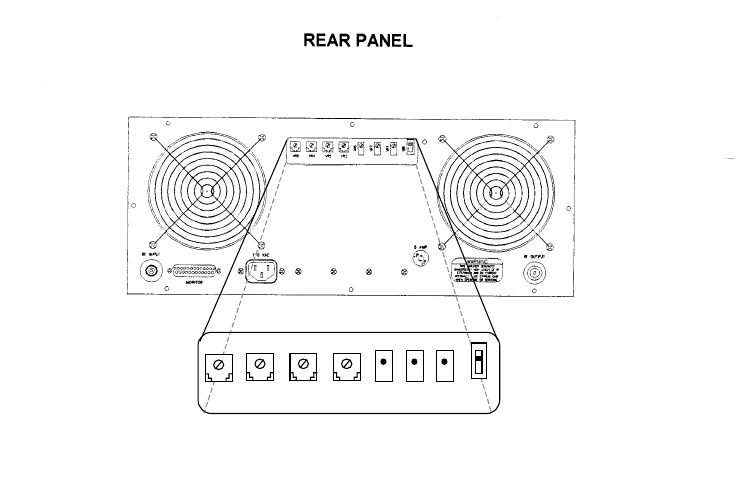
120 20170-302 ParagonPD Technical Manual
37
b) Toggle the front panel switch until the top line of the display reads RFL PWR.
c) Key the transmitter T881's Exciter Carrier button.
d) Adjust TPL's VR7 so that the front panel meter is in agreement with the calibrated power meter.
5.2.5.7 Reverse Power Alarm Level
a) Connect an unterminated 3dB pad to the PA output (e.g. 3:1 VSWR).
e) Key the transmitter T881's Exciter Carrier button.
b) Adjust TPL's VR3 until the front panel SWR LED begins to flash
Note: The LED should extinguish when the normal load is connected (connected to IFR).
Figure 26 - (TPL) LMS Rear Panel
VR8 VR4 VR5 VR3 VR6 VR7 VR1 SW1
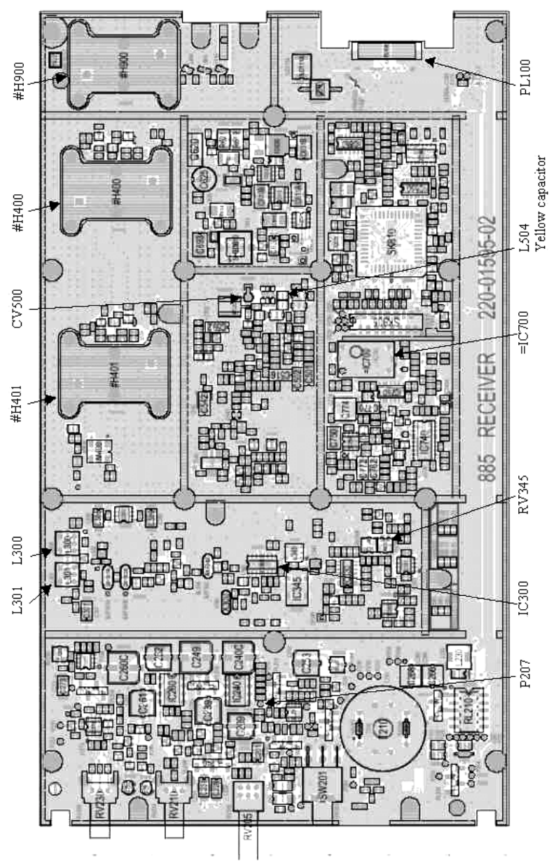
120 20170-302 ParagonPD Technical Manual
38
-
Figure 27 - T885-0020 Receiver Tuning Controls Location
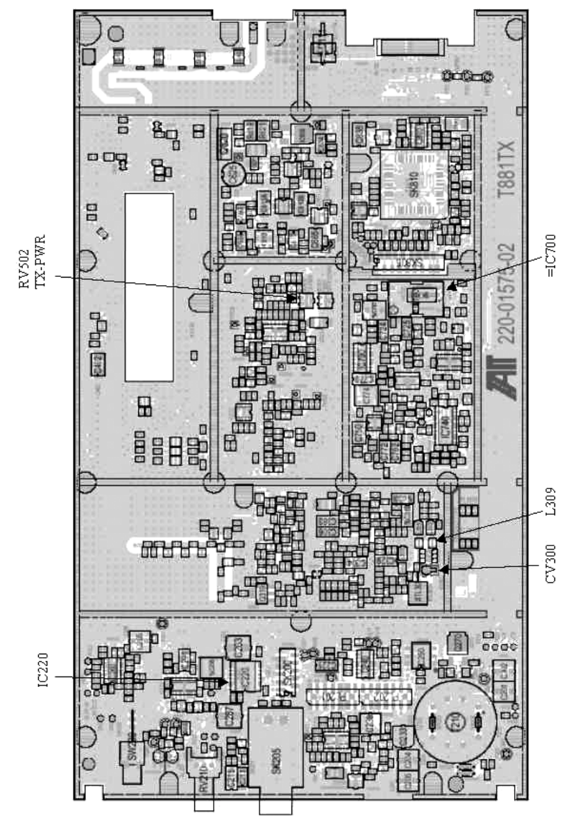
120 20170-302 ParagonPD Technical Manual
39
Figure 28 - T881-0200 Exciter Tuning Controls Locations
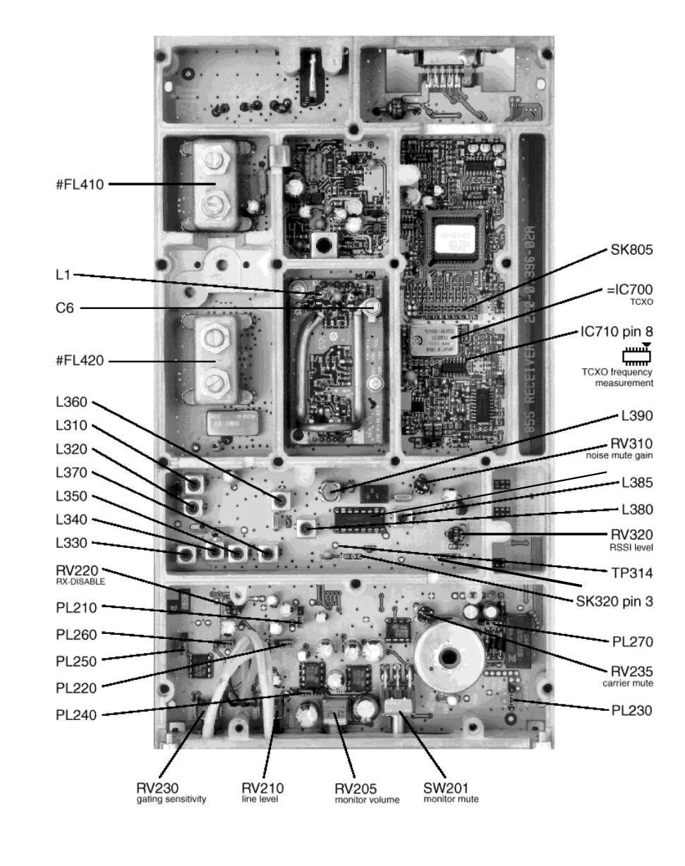
120 20170-302 ParagonPD Technical Manual
40
Figure 29 - T855 Receiver Tuning Controls Location
IC 310
SK330 pin 2
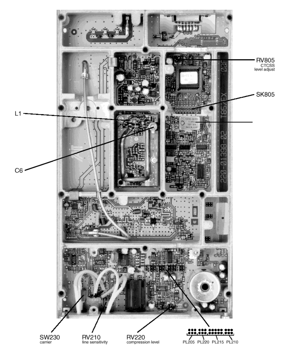
120 20170-302 ParagonPD Technical Manual
41
Figure 30 - T857 Exciter Tuning Controls Locations
TCXO
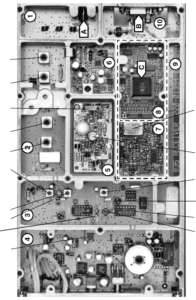
120 20170-302 ParagonPD Technical Manual
42
Figure 31 - T835 Receiver Tuning Controls Location
RV 320
L410
L420
L1
L460
L470
CV318
L340
RSSI
Test Point
P207
IC 700
CV1
L350
IC 350
L360
L330
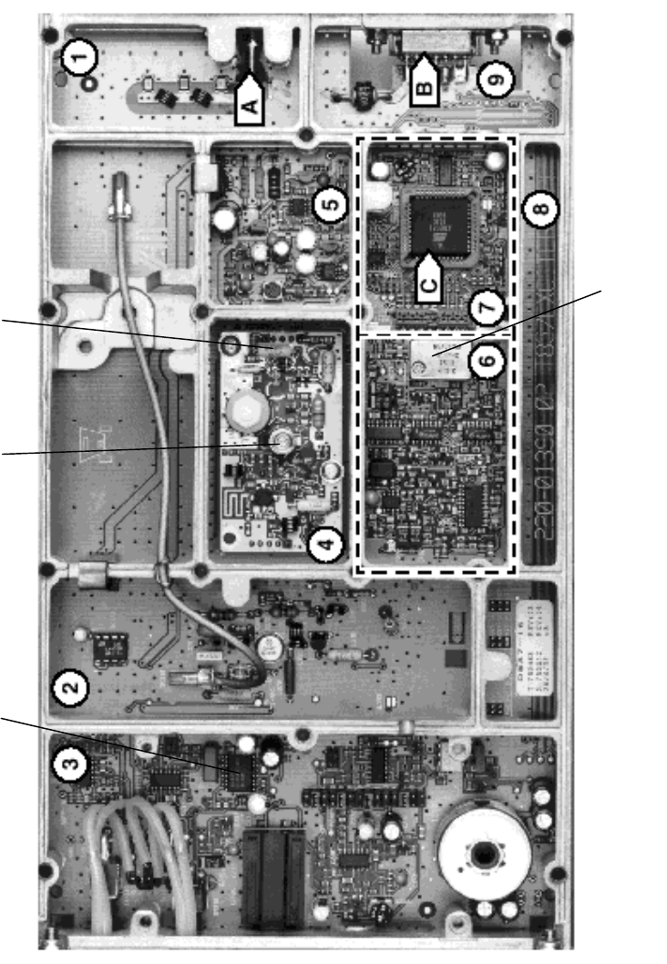
120 20170-302 ParagonPD Technical Manual
43
Figure 32 - T837 Exciter Tuning Controls Location
L1
CV1
IC220
IC700
TCXO
120 20170-302 ParagonPD Technical Manual
44
Appendix 1 - ParagonPD Deviation adjust
1. Using the WinRIS, press TX ON (Modulated) and record deviation level as read on the IFR.
2. Using Windows Notepad, Edit the .bp2 file named with the corresponding BDLCPD serial
number (e.g. abcd.bp2). “Save as” to another file name and keep it in case something goes
wrong while changing a parameter.
3. Locate the line labeled “Dev0 Par85=” and record the value beside the “=” sign. This is the
corresponding parameter value to the deviation read in step 1.
4. Apply the following formula to determine the new parameter value to be set:
(New Par85 value) = [(initial Par85 value) X (target deviation) / (deviation read)] + 2
5. Change the value in the file, “Save as” using the BDLCPD serial number file name.
6. Run the WinRIS again and do a “Put From”. From the opened window, select the file that
you just made the change to and then press “OK”
7. Again, check deviation level while pressing TX ON (Modulated).
• If the level is now correct, press StationReset to make the change permanent.
• Otherwise do step 5 again, changing the value entered in the file by 1 or 2 digit(s) up
or down, fine-tuning directly the Par85 (DSP deviation) parameter. Do steps 6 and 7
again to confirm acceptance.
This last step may have to be repeated once or twice while varying the entered value
up or down. If unable to obtain the correct level after editing up and/or down by no
more than 2, contact System Engineering.
120 20170-302 ParagonPD Technical Manual
45
6. Specifications
GENERAL
VHF UHF 800 900
Frequency 136 -156 MHz
148 -174 MHz
400 - 440 MHz1
440 - 480 MHz
480 - 520 MHz
RX 800 - 870 MHz
TX 850 - 870 MHz
RX 890 - 960 MHz
TX 890 - 960 MHz
RF/Modem Assembly Size 19.0” W x 17.5.0” H x 12.5” D + 2.0” connector allowance
Frequency Stability 2.5 ppm (-30 to +60ºC) 1.0 ppm (-20 to +60ºC)
Supply Voltage
13.8 VDC nominal (negative ground), 10.8 - 16 VDC
or
115 VAC
Circuit protection
Fuse 1: 32-volt MDL (slow-blow) 10A
Fuse 2: 32-volt MDL (slow-blow) 30A
Crowbar diodes for reverse polarity protection
RX Current Consumption @ 13.8
VDC 1.5A max. (Two receivers with speaker monitoring)
TX Current Consumption @ 13.8 VDC 20A (16A typical @
156MHz for 100W) 24A (22A DC typical @
450MHz for 100W) 28A (23A DC typical @ 850MHz for
70W)
Base Station Power Consumption
@ 115 VAC 6A max.
Channel spacing 25 kHz and 12.5 kHz
Operating Temperature Range -30°C to +60°C (deleted power supply, catalog number ending with a 0)
-10°C to +60°C (with standard Dual Power Supply assembly, catalog number ending with a 2)
RECEIVER
Selectivity @ 25 kHz
@ 12.5 kHz
92 dB min, 95 dB (Typical)
86 dB min, 89 dB (Typical)
87 dB min, 90 dB (Typical)
83 dB min, 85 dB (Typical)
85 dB min, 88 dB (Typical)
79 dB min, 80 dB (Typical)
Sensitivity @ 12 dB SINAD -117 dBm*
Spurious Response Rejection 100 dB (Typical)
Intermodulation Rejection
- EIA (25 kHz)
- EIA 300-096 (12.5 kHz) 85 dB (Typical)
80 dB (Typical)
85 dB (Typical)
80 dB (Typical)
80 dB (Typical)
75 dB (Typical)
Hum and Noise
- EIA (25 kHz)
- ETS 300-096 (12.5 kHz) 55 dB*
50 dB*
47 dB*
45 dB*
* Psophometrically weighted (De-emphasis response)
TRANSMITTER
Rated Continuous RF Power 100W 100W 70W
Range of Adjustment 20 – 100 W 20 – 100 W 20 – 70 W 65 - 100 W
Spurious Emissions: - transmit
- standby
-36 dBm to 1GHz, -30 dBm to 4 GHz (to 3.2GHz for 800/900 model)
-57 dBm to 1GHz, -47 dBm to 4 GHz ((to 3.2GHz for 800/900 model))
VSWR Stability 5:1 mismatch
Transmitter Sideband Noise
@ +/-25 kHz
@ +/- 1 MHz
-95 dBc
-105 dBc
-95 dBc
-105 dBc
-88 dBc
-100 dBc
1 WARNING: The frequency band 406 to 406.1 MHz is reserved for use by distress beacons and should not be programmed into
the unit.
120 20170-302 ParagonPD Technical Manual
46
Data rates and Modulation type*
Channel type
32 kb/s
(RC4FSK)
GeminiPD+ only
25.6 kb/s
(SRRC4FSK)
19.2 kb/s
(SRRC4FSK)
19.2 kb/s
(DGMSK)
16 kb/s
(SRRC4FSK)
14.4 kb/s
(SRRC4FSK)
VHF (25 kHz) TBD TBD NA -113 dBm N/A N/A
VHF (12.5kHz) N/A N/A N/A N/A TBD TBD
UHF (25 kHz) -107 dBm -110 dBm N/A -113 dBm N/A N/A
UHF (12.5kHz) N/A N/A N/A N/A -109 dBm -112 dBm
800 (25 kHz) -108 dBm -109 dBm N/A -113 dBm N/A N/A
800 (NPSPAC) N/A N/A -108 dBm -108 dBm -112 dBm N/A
800 (12.5kHz) N/A N/A N/A N/A -110 dBm -113 dBm
Packet Error Rate
(< 1% error, at Fc,
with Parallel Decode)
900 (12.5kHz) N/A N/A TBD TBD TBD TBD
Protocol Dataradio Proprietary DBA
Operation Full duplex
* Networks must use common modulation, bit and baud rates. Different types are not on-air compatible
FCC / IC CERTIFICATIONS
FCC IC (DOC) *
VHF 136 - 156 MHz
148 - 174 MHz
CASTEL0007
EOTBDD4T83-2
737195375A
737195376A
400 - 440 MHz EOTBDD4T85-1
UHF 440 - 480 MHz EOTBDD4T85-2 3993195401A
480 - 520 MHz EOTBDD4T85-3 N/A
800 MHz
Series II 800 - 870 MHz EOTBDD4T881S2 (4Watts)
EOTBDD4T889 (100 Watts) 737194358
900 MHz
Series II 890 - 960 MHz EOTBD4T881-3 (4 Watts)
BBD8-2BF-L (100 Watts, TPL) 737194358
* Operating under Class II permissive change
EMISSION DESIGNATORS*
Bit
rate Baud rate Modulation VHF UHF 800MHz 900MHz
32000 16000 RC4FSK 15K2F1D 16K5F1D 15K9F1D -
25600 12800 SRRC4FSK 14K7F1D 14K3F1D 14K3F1D -
19200 9600 SRRC4FSK - 15K9F1D 15K9F1D 9K58F1D
16000 8000 SRRC4FSK 7K67F1D 7K00F1D 9K50F1D 9K75F1D
14400 7200 SRRC4FSK 8K25F1D 7K50F1D 11K0F1D 10K9F1D
* Emission designators for legacy DGMSK modulations are available on certificates