Casambi Technologies CBM002A Bluetooth 4.0 Module User Manual
Casambi Technologies Oy Bluetooth 4.0 Module
UserManual.wiki
>
Casambi Technologies
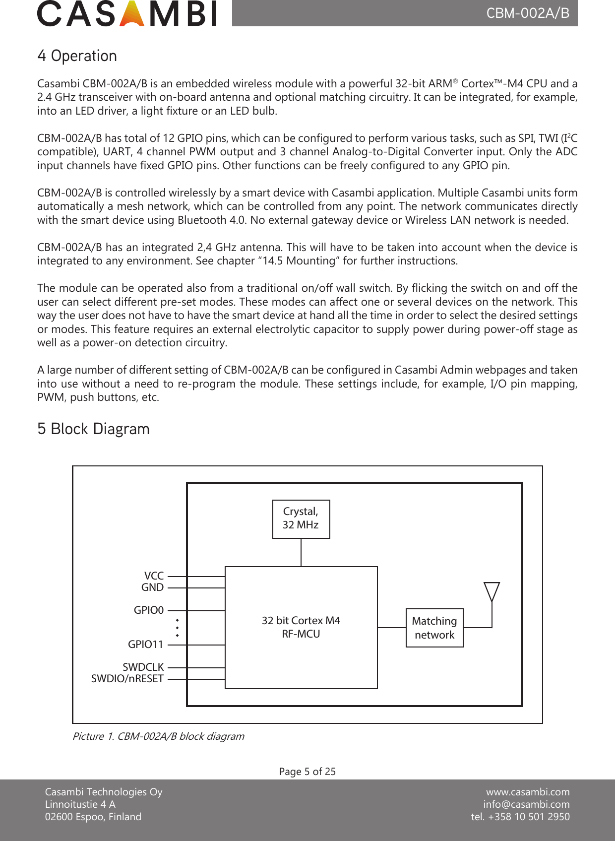
>
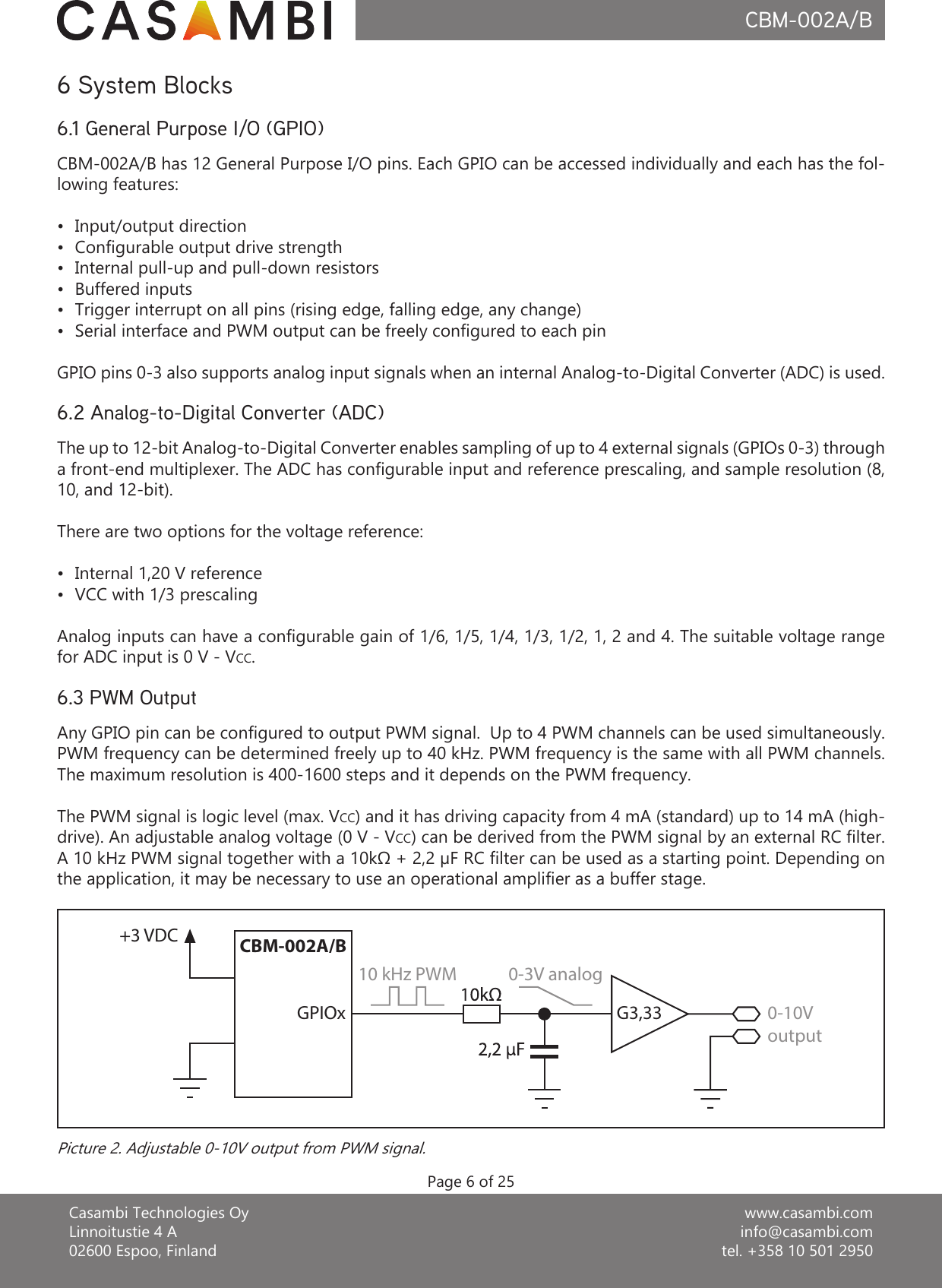
CBM002A User Manual
User Manual
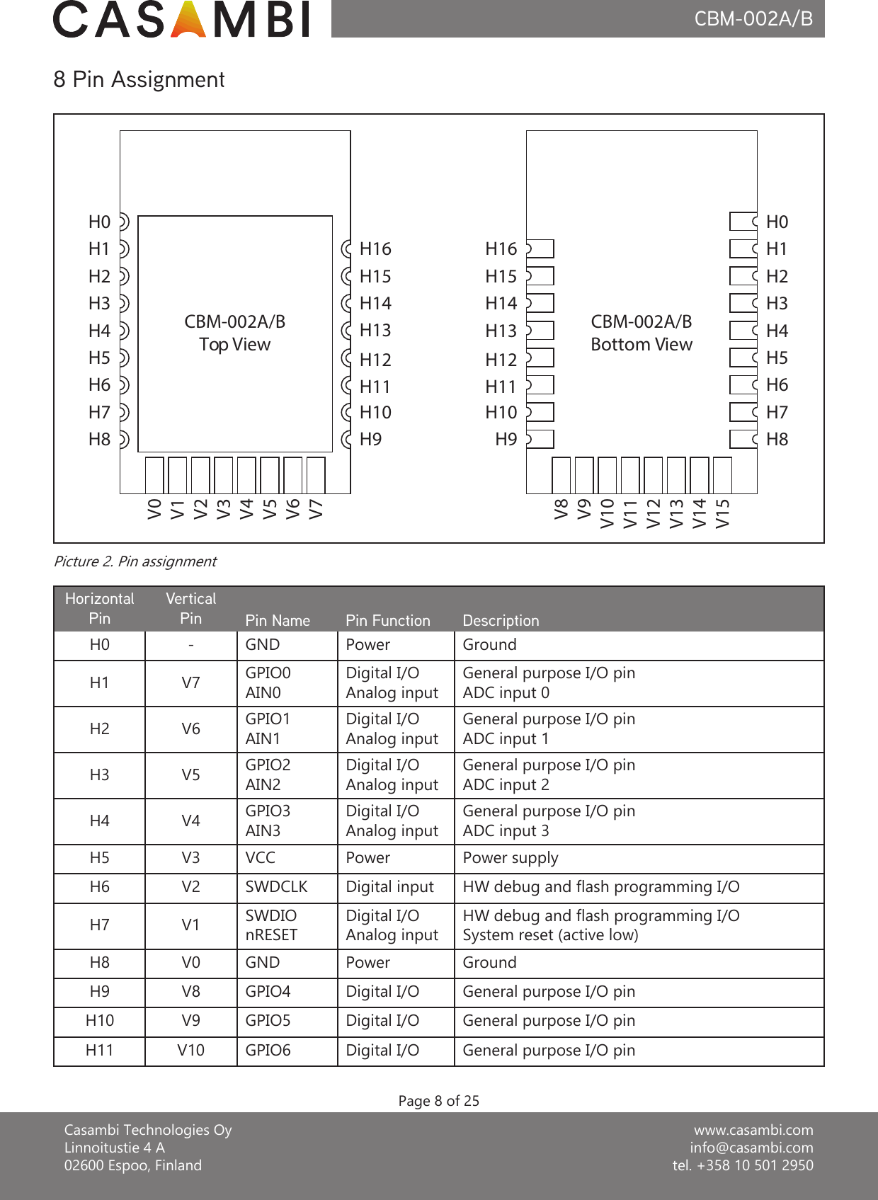
Navigation menu
Upload a User Manual
Namespaces
Wiki Guide
HTML
PDF
Info
Views
User Manual
Discussion / Help
Navigation