Casambi Technologies CBM002B Bluetooth 4.0 Module User Manual Installation Guide
Casambi Technologies Oy Bluetooth 4.0 Module Installation Guide
Installation Guide
www.casambi.com
info@casambi.com
tel. +358 10 501 2950
Casambi Technologies Oy
Linnoitustie 4 A
02600 Espoo, Finland
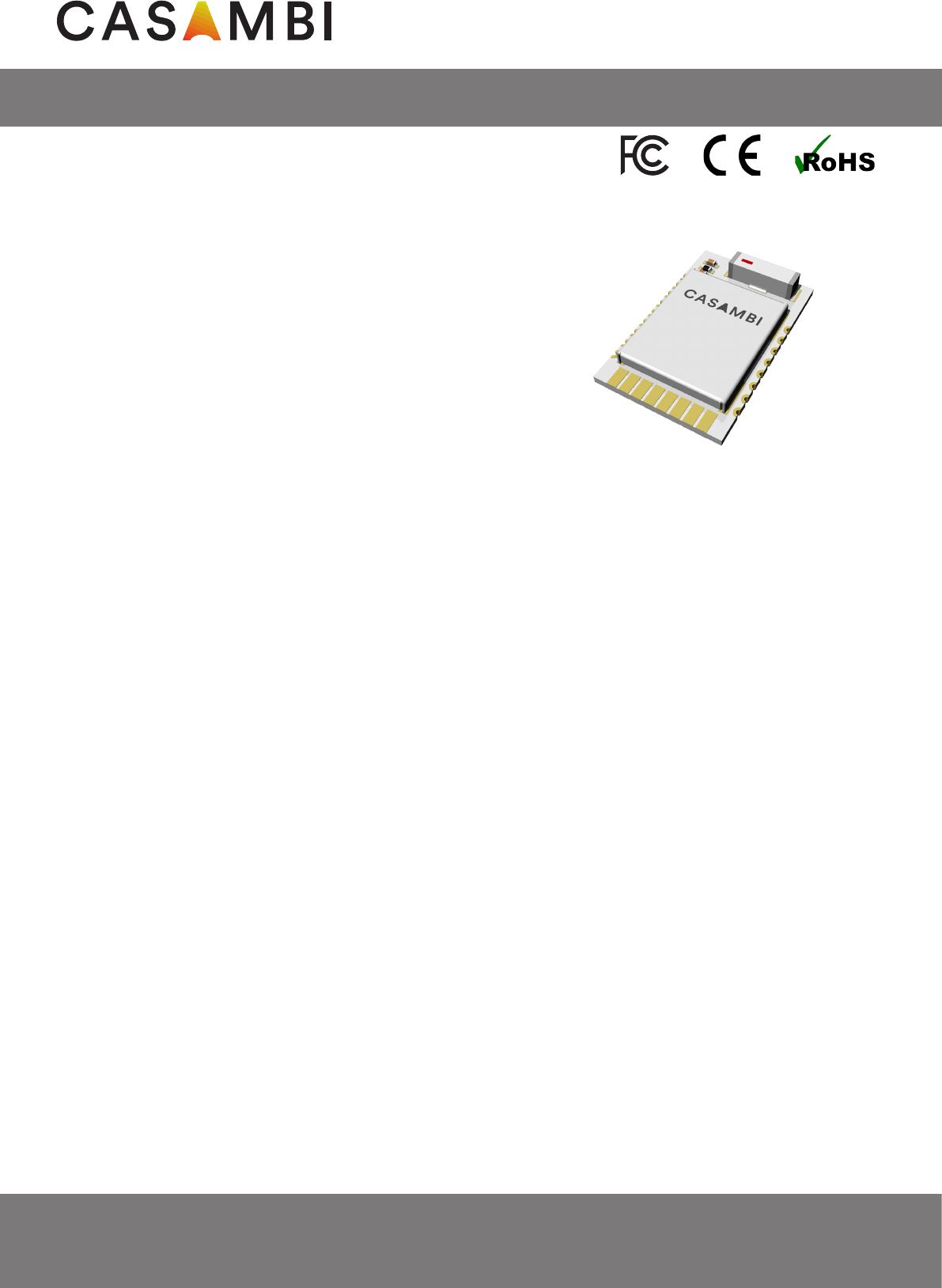
Casambi CBM-002A/B
CBM-002A/B is a Class 2 embedded Bluetooth 4.0 module designed to be integrated into LED drivers, differ-
ent lighting control applications, light xtures and LED bulbs. It is pre-programmed with Casambi’s propri-
etary rmware making it completely compatible with other Casambi enable devices.
CBM-002A/B is controlled wirelessly with Casambi smartphone and tablet applications using Bluetooth 4.0
protocol. Devices form automatically a self-healing and self-organizing wireless mesh network so that a large
number of xtures can be controlled from any point. No external gateway module is needed.
CBM-002A/B contains a powerful 32-bit ARM® Cortex™-M4 CPU and a 2.4 GHz transceiver with on-board
antenna and optional matching circuitry. Different external components, such as motion detectors, ambient
light sensors and PWM circuits, can be interfaced with the module by using its 12 general purpose I/O pins.
CBM-002A/B can be mounted both in horizontal and vertical position making it very versatile for projects with
different form-factors.
Casambi Lighting Control System:
• Wirelessly controllable with a Bluetooth 4.0 smart device
• No need for external gateway device
• Forms automatically a wireless mesh network
• Device rmware can be updated over-the-air
• Casambi cloud service available
• Extremely easy set-up
CBM-002A/B Features:
• Small form factor, 12,7 mm x 20,0 mm x 2,85 mm
• 12 pcs general purpose input/output pins
• SPI, TWI, UART, PWM (max. 4 ch)
• Integrated antenna, two different versions
• Up to 4 dBm output power and -93 dBm RX sensitivity
• Range up to 50 m in open air
• Can be mounted in horizontal or vertical position
• Delivered pre-loaded with Casambi rmware
Features
Product Specication
1 Description
• LED drivers, 1-4 channels
• Different lighting control applications
• Light xtures
• Single and multicolor LED bulbs
Applications
Page 1 of 25
www.casambi.com
info@casambi.com
tel. +358 10 501 2950
Casambi Technologies Oy
Linnoitustie 4 A
02600 Espoo, Finland
CBM-002A/B
Version
March 2017
Description
1.0 Original version
October 2017 1.1 Compliance information updated
November 2017 1.2 Compliance information updated
Date
2 Revision history
Page 2 of 25
CBM-002A
Description
CBM-002 with on-board SMD chip antenna
CBM-002B CBM-002 with on-board wire antenna
Part Number
3 Ordering Information

www.casambi.com
info@casambi.com
tel. +358 10 501 2950
Casambi Technologies Oy
Linnoitustie 4 A
02600 Espoo, Finland
CBM-002A/B
Table of Contents
1Description .............................................................................................................................................. 1
2Revision History .................................................................................................................................... 2
4
3
Operation
Ordering Information
................................................................................................................................................ 5
......................................................................................................................... 2
Page 3 of 25
5 Block Diagram ....................................................................................................................................... 5
6System Blocks ........................................................................................................................................ 6
6.1 General Purpose I/O (GPIO) ............................................................................................................. 6
6.2 Analog-to-Digital Converter (ADC) ............................................................................................... 6
6.3 PWM Output .......................................................................................................................................... 6
7.1 Serial Peripheral Interface (SPI) ....................................................................................................... 7
7.2 Two-Wire Interface (TWI) .................................................................................................................. 7
7.3 Universal Asynchronous Receiver/Transmitter (UART) .......................................................... 7
7 Serial Interfaces ..................................................................................................................................... 7
9 Electrical Specications ...................................................................................................................... 9
9.1 Absolute Maximum Ratings ............................................................................................................. 9
9.2 Power Supply Specications ............................................................................................................ 9
9.3 GPIO Specications ........................................................................................................................... 10
10 Environmental Conditions .............................................................................................................. 10
11 Radio Characteristics ........................................................................................................................ 10
11.1 General Radio Characteristics ....................................................................................................... 10
12 Communication Interface Characteristics ................................................................................ 11
12.1 Bit Rates ................................................................................................................................................. 11
12.2 SPI Specications ............................................................................................................................... 11
12.3 TWI Specications ............................................................................................................................. 12
13 PWM Specications .......................................................................................................................... 12
14 Application Information .................................................................................................................. 13
14.1 Smart Switching .................................................................................................................................. 13
14.2
14.3
14.3.1 CBM-002B Antenna ........................................................................................................................ 16
Antenna Versions ............................................................................................................................... 15
Power-On Detection ......................................................................................................................... 14
8 Pin Assignment ..................................................................................................................................... 8
14.4 Mounting .............................................................................................................................................. 16
14.4.1 Horizontal Mounting ........................................................................................................................ 17
14.4.2 Vertical Mounting .............................................................................................................................. 18
15 Mechanical Specications .............................................................................................................. 18

www.casambi.com
info@casambi.com
tel. +358 10 501 2950
Casambi Technologies Oy
Linnoitustie 4 A
02600 Espoo, Finland
CBM-002A/B
Page 4 of 25
16 Soldering ............................................................................................................................................... 19
16.1 Leaded Reow Soldering ................................................................................................................ 19
16.2 Leadfree Reow Soldering ............................................................................................................. 19
16.3 Hand Soldering ................................................................................................................................... 20
16.4 Rework ................................................................................................................................................... 20
16.5 Cleaning ................................................................................................................................................. 20
17 Compliance Information ................................................................................................................. 20
17.1 FCC Statement .................................................................................................................................... 21
17.2 ISED Statement ................................................................................................................................... 22
17.3 CE Declaration of Conformity ....................................................................................................... 25
www.casambi.com
info@casambi.com
tel. +358 10 501 2950
Casambi Technologies Oy
Linnoitustie 4 A
02600 Espoo, Finland
CBM-002A/B
4 Operation
Casambi CBM-002A/B is an embedded wireless module with a powerful 32-bit ARM® Cortex™-M4 CPU and a
2.4 GHz transceiver with on-board antenna and optional matching circuitry. It can be integrated, for example,
into an LED driver, a light xture or an LED bulb.
CBM-002A/B has total of 12 GPIO pins, which can be congured to perform various tasks, such as SPI, TWI (I2C
compatible), UART, 4 channel PWM output and 3 channel Analog-to-Digital Converter input. Only the ADC
input channels have xed GPIO pins. Other functions can be freely congured to any GPIO pin.
CBM-002A/B is controlled wirelessly by a smart device with Casambi application. Multiple Casambi units form
automatically a mesh network, which can be controlled from any point. The network communicates directly
with the smart device using Bluetooth 4.0. No external gateway device or Wireless LAN network is needed.
CBM-002A/B has an integrated 2,4 GHz antenna. This will have to be taken into account when the device is
integrated to any environment. See chapter “14.5 Mounting” for further instructions.
The module can be operated also from a traditional on/off wall switch. By icking the switch on and off the
user can select different pre-set modes. These modes can affect one or several devices on the network. This
way the user does not have to have the smart device at hand all the time in order to select the desired settings
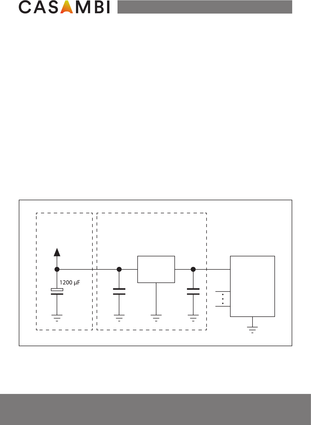
or modes. This feature requires an external electrolytic capacitor to supply power during power-off stage as
well as a power-on detection circuitry.
A large number of different setting of CBM-002A/B can be congured in Casambi Admin webpages and taken
into use without a need to re-program the module. These settings include, for example, I/O pin mapping,
PWM, push buttons, etc.
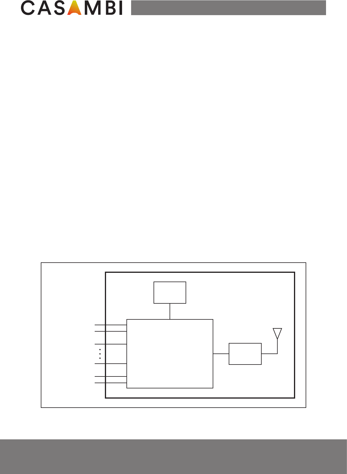
5 Block Diagram
Picture 1. CBM-002A/B block diagram
Page 5 of 25
Crystal,
32 MHz
Matching
network
32 bit Cortex M4
RF-MCU
VCC
GND
GPIO0
GPIO11
SWDCLK
SWDIO/nRESET

www.casambi.com
info@casambi.com
tel. +358 10 501 2950
Casambi Technologies Oy
Linnoitustie 4 A
02600 Espoo, Finland
CBM-002A/B
6 System Blocks
CBM-002A/B has 12 General Purpose I/O pins. Each GPIO can be accessed individually and each has the fol-
lowing features:
• Input/output direction
• Congurable output drive strength
• Internal pull-up and pull-down resistors
• Buffered inputs
• Trigger interrupt on all pins (rising edge, falling edge, any change)
• Serial interface and PWM output can be freely congured to each pin
GPIO pins 0-3 also supports analog input signals when an internal Analog-to-Digital Converter (ADC) is used.
The up to 12-bit Analog-to-Digital Converter enables sampling of up to 4 external signals (GPIOs 0-3) through
a front-end multiplexer. The ADC has congurable input and reference prescaling, and sample resolution (8,
10, and 12-bit).
There are two options for the voltage reference:
• Internal 1,20 V reference
• VCC with 1/3 prescaling
Analog inputs can have a congurable gain of 1/6, 1/5, 1/4, 1/3, 1/2, 1, 2 and 4. The suitable voltage range
for ADC input is 0 V - VCC.
Any GPIO pin can be congured to output PWM signal. Up to 4 PWM channels can be used simultaneously.
PWM frequency can be determined freely up to 40 kHz. PWM frequency is the same with all PWM channels.
The maximum resolution is 400-1600 steps and it depends on the PWM frequency.
The PWM signal is logic level (max. VCC) and it has driving capacity from 4 mA (standard) up to 14 mA (high-
drive). An adjustable analog voltage (0 V - VCC) can be derived from the PWM signal by an external RC lter.
A 10 kHz PWM signal together with a 10kΩ + 2,2 µF RC filter can be used as a starting point. Depending on
the application, it may be necessary to use an operational amplifier as a buffer stage.
Page 6 of 25
6.1 General Purpose I/O (GPIO)
6.2 Analog-to-Digital Converter (ADC)
6.3 PWM Output
Picture 2. Adjustable 0-10V output from PWM signal.
CBM-002A/B
GPIOx
10 kHz PWM 0-3V analog
+3 VDC
G3,33 0-10V
output

www.casambi.com
info@casambi.com
tel. +358 10 501 2950
Casambi Technologies Oy
Linnoitustie 4 A
02600 Espoo, Finland
CBM-002A/B
7 Serial Interfaces
CBM-002A/B supports a 3-wire (SCK, MISO, MOSI) bidirectional SPI bus with fast data transfers to and from
multiple slaves. CBM-002A/B acts as a master and it provides a simple CPU interface which includes a TXD
register for sending data and an RXD register for receiving data. These registers are double-buffered to en-
able some degree of uninterrupted data ow in and out of the SPI master.
Each of the slave devices requires an individual chip select signal which can be connected to any available
GPIO pin. The SPI master does not implement support for chip select directly. Therefore, the correct slave
must be selected independently of the SPI master.
The GPIOs used for each SPI interface line can be chosen from any GPIO on the module and are indepen-
dently congurable. This enables great exibility in module pinout and enables efcient use of printed circuit
board space and signal routing.
The SPI peripheral supports SPI modes 0, 1, 2, and 3.
7.1 Serial Peripheral Interface (SPI)
The Two-Wire Interface (I2C compatible) can interface a bidirectional wired-AND bus with two lines (SCL,
SDA). The interface is capable of clock stretching and data rates of 100 kbps and 400 kbps are supported. The
TWI transmitter and receiver are single buffered.
The GPIOs used for each Two-Wire Interface line can be chosen from any GPIO on the module and are in-
dependently congurable. This enables great exibility in module pin-out and enables efcient use of board
space and signal routing.
7.2 Two-Wire Interface (TWI)
The Universal Asynchronous Receiver/Transmitter offers fast, full-duplex, asynchronous serial communication
with built-in ow control support in HW up to 1 Mbps baud. Parity checking and generation for the 9th data
bit are supported.
The GPIOs used for each UART interface line can be chosen from any GPIO on the module and are indepen-
dently congurable. This enables great exibility in module pinout and enables efcient use of board space
and signal routing.
7.3 Universal Asynchronous Receiver/Transmitter (UART)
CBM-002A/B can be connected to an external MCU through its extension interface, which supports SPI, TWI
and UART. Through this interface it is possible to, for example, gather information from sensors through
Casambi network.
Page 7 of 25
www.casambi.com
info@casambi.com
tel. +358 10 501 2950
Casambi Technologies Oy
Linnoitustie 4 A
02600 Espoo, Finland
CBM-002A/B
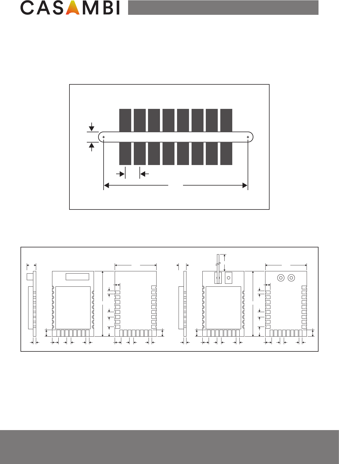
8 Pin Assignment
Horizontal
Pin
Vertical
Pin Pin Name Pin Function Description
H0 -GND Power Ground
H1 V7 GPIO0
AIN0
Digital I/O
Analog input
General purpose I/O pin
ADC input 0
H2 V6 GPIO1
AIN1
Digital I/O
Analog input
General purpose I/O pin
ADC input 1
H3 V5 GPIO2
AIN2
Digital I/O
Analog input
General purpose I/O pin
ADC input 2
H4 V4 GPIO3
AIN3
Digital I/O
Analog input
General purpose I/O pin
ADC input 3
H5 V3 VCC Power Power supply
H6 V2 SWDCLK Digital input HW debug and ash programming I/O
H7 V1 SWDIO
nRESET
Digital I/O
Analog input
HW debug and ash programming I/O
System reset (active low)
H8 V0 GND Power Ground
H9 V8 GPIO4 Digital I/O General purpose I/O pin
H10 V9 GPIO5 Digital I/O General purpose I/O pin
H11 V10 GPIO6 Digital I/O General purpose I/O pin
Picture 2. Pin assignment
Page 8 of 25
H0
H1
H2
H3
H4
H5
H6
H7
H8
H10
H9
H11
H12
H13
H14
H15
H16
V0
V1
V2
V3
V4
V5
V6
V7
H10
H9
H11
H12
H13
H14
H15
H16
H0
H1
H2
H3
H4
H5
H6
H7
H8
V8
V9
V10
V11
V12
V13
V14
V15
CBM-002A/B
Top View
CBM-002A/B
Bottom View
www.casambi.com
info@casambi.com
tel. +358 10 501 2950
Casambi Technologies Oy
Linnoitustie 4 A
02600 Espoo, Finland
CBM-002A/B
Min.
Supply voltage, VCC
Typ. Units
+2,5 +3,0 V
Supply current, ICC 7mA
Power Supply Specications Max.
+3,6
Horizontal
Pin
Vertical
Pin Pin Name Pin Function Description
H13 V12 GPIO8 Digital I/O General purpose I/O pin
H14 V13 GPIO9 Digital I/O General purpose I/O pin
H15 V14 GPIO10 Digital I/O General purpose I/O pin
H16 V15 GPIO11 Digital I/O General purpose I/O pin
H12 V11 GPIO7 Digital I/O General purpose I/O pin
Table 1. Pin assignment
Table 3. Power supply specications
Min.
Supply voltage, VCC
Maximum ratings are the extreme limits to which CBM-002A/B can be exposed without permanently damag-
ing it. Exposure to absolute maximum ratings for prolonged periods of time may affect the reliability.
Max. Units
-0,3 +3,9 V
GND 0 V
I/O pin voltage, VIO -0,3 VCC + 0,3 V
Storage temperature -40 +125 °C
Operating temperature, TA-25 +85 °C
Absolute Maximum Ratings
Table 2. Absolute maximum ratings
Page 9 of 25
9 Electrical Specications
9.1 Absolute Maximum Ratings
9.2 Power Supply Specications
www.casambi.com
info@casambi.com
tel. +358 10 501 2950
Casambi Technologies Oy
Linnoitustie 4 A
02600 Espoo, Finland
CBM-002A/B
Min.
Input high voltage, VIH
Typ. Units
0,7xVCC V
Input low voltage, VIL GND V
Output high voltage, VOH VCC-0,4 V
Output low voltage, VOL GND V
GPIO Specications Max.
VCC
0,3xVCC
VCC
0,4
Source current, IGPIO_OUT 12 mA14 1)
Sink current, IGPIO_IN 12 mA15 1)
Pull-up resistance, RPU 11 13 kΩ16
Pull-down resistance, RPD 11 13 kΩ16
1) If required source/sink current in any GPIO pin is more than 4 mA, corresponding GPIO pin must be congured as high-drive.
Table 4. GPIO specications
11 Radio Characteristics
Min.
Operating frequencies, fOP, 1 MHz chann. spacing
Typ. Units
2402 MHz
PLL programming resolution, PLLres 1 MHz
Frequency deviation, ∆fBLE ±225 ±250 kHz
On-air data rate, bpsFSK 1000 kbps
General Radio Characteristics Max.
2483
±275
2000
11.1 General Radio Characteristics
Min.
Storage temperature
Typ. Units
-40 °C
Operating temperature, TA-25 +25 °C
Relative humidity, storage %
Relative humidity, operating %
Environmental Conditions Max.
+125
+85
90
80
Table 5. Environmental conditions
Table 6. General radio characteristics
Page 10 of 25
9.3 General Purpose I/O Specications
10 Environmental Conditions
Maximum output power, PRF +4 dBm
Sensitivity, PSENS -89 dBm-93
www.casambi.com
info@casambi.com
tel. +358 10 501 2950
Casambi Technologies Oy
Linnoitustie 4 A
02600 Espoo, Finland
CBM-002A/B
12 Communication Interface Characteristics
Min.
Bit rate for SPI, fSPI
Typ. Units
0,125 Mbps
Bit rates for TWI, f2W 100 kbps
Baud rate for UART, fUART 1,2 kbps
Bit Rates Max.
8
400
1000
12.1 Bit Rates
Table 9. UART specications
Page 11 of 25
12.2 SPI Timing Parameters
Min.
Data to SCK setup, tDC
Typ. Units
10 ns
SCK to Data hold, tDH 10 ns
SCK to Data valid, tCD 60 ns
SCK High time, tCH 40 ns
SPI Timing Parameters Max.
80
SCK Low time, tCL 40 ns
SCK Frequency, fSCK 0,125 MHz8
SCK Rise and Fall time, tR, tFns100
tDC
tDH
tCD
tCH tCL
b7b6b0
b7b0
SCK
MISO
MOSI
Picture 3. SPI timing diagram, one byte transmission, SPI mode 0
Table 11. SPI timing parameters
www.casambi.com
info@casambi.com
tel. +358 10 501 2950
Casambi Technologies Oy
Linnoitustie 4 A
02600 Espoo, Finland
CBM-002A/B
Page 12 of 25
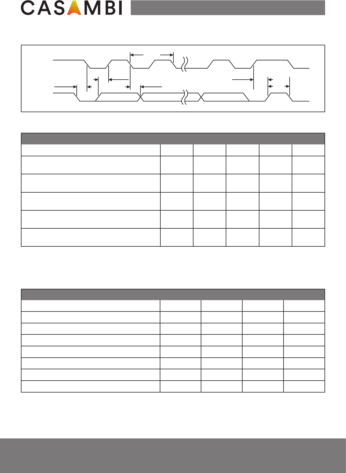
12.3 TWI Timing Parameters
Min.
SCL clock frequency, fSCL
Units
100 kHz
Hold time for START and repeated
START condition, tHD_STA 5200
TWI Timing Parameters
400
Max. Min. Max.
Standard Fast
1300 ns
Data setup time before positive
edge on SCL, tSU_DAT 300 300 ns
Data hold time after negative
edge on SCL, tHD_DAT 300 300 ns
Setup time from SCL goes high
to STOP condition, tSU_STO 5200 1300 ns
Bus free time between STOP and
START conditions, tBUF 4700 1300 ns
tHD_SDA
tSU_DAT
tHD_DAT
1/fSCL
SCL
SDA
tSU_STO
tBUF
Picture 4. TWI SCL/SDA timing
Table 13. TWI timing parameters
Min.
PWM frequency, fPWM
Typ. Units
kHz
PWM sink/source current, IPWM 2 mA
PWM resolution 400 steps
PWM Specications Max.
40
14 1)
1600
13 PWM Specications
PWM resolution @ fPWM 10 kHz steps1600
PWM resolution @ fPWM 20 kHz steps800
1) If required source/sink current in any GPIO pin is more than 4 mA, corresponding GPIO pin must be congured as high-drive.
PWM resolution @ fPWM 40 kHz steps400
PWM high output voltage, VPWM_H VCC-0,4 VVCC
PWM low output voltage, VPWM_L GND V0,4
Table 16. PWM specications
www.casambi.com
info@casambi.com
tel. +358 10 501 2950
Casambi Technologies Oy
Linnoitustie 4 A
02600 Espoo, Finland
CBM-002A/B
Page 13 of 25
14 Application Information
Casambi has developed a solution for controlling lighting with only a traditional on/off wall switch. By default,
the wall switch can be used to dim the lights, but different settings can be selected from Casambi App, such as
selecting a pre-set mode. With Smart Switching feature, multiple lights can be controlled from a single switch.
Smart Switching feature is used by icking the wall switch quickly off and on.
Smart Switching is a function which requires an external electrolytic bypass capacitor and a power-on detec-
tion circuitry to work. The external electrolytic capacitor is needed to supply the necessary operating voltage
for the module during power-off stage. It can be either an external capacitor just for the CBM-002A/B, or
it can be a part of a larger power supply on the host board. If the capacitor is dedicated just for the CBM-
002A/B, the minimum required capacitance is 1200 µF. It is advisable to connect the capacitor before any
voltage regulation for larger voltage drop.
Even if Smart Switching feature is not used, the correct use of CBM-002A/B still requires the power-on detec-
tion and the external capacitor. These are needed so that the module can inform Casambi network when its
power is cut off. The external capacitor will provide power to the module a short time after the power has
been switched off. A suitable time for Smart Switching is 1,5 seconds and without Smart Switching 0,5 sec-
onds. The external capacitor will have to be sized according to these requirements.
It is a good practice to use a capacitor with temperature range up to 105°C.
14.1 Smart Switching
Picture 7. Powering CBM-002A/B with an external capacitor for Smart Switching
Vcc
GPIOs
CBM-002A/B
Linear
regulator,
Vout 3,0 V
CinC out
Basic linear regulator circuitBypass capacitor
for Smart Switching

www.casambi.com
info@casambi.com
tel. +358 10 501 2950
Casambi Technologies Oy
Linnoitustie 4 A
02600 Espoo, Finland
CBM-002A/B
Page 14 of 25
In order to operate correctly, the Casambi network will have to know if the power has been switched off from
some unit. For this reason, the unit will have to know when its power has been switched off. This is done by a
power-on detection together with an external capacitor (see previous chapter).
In case of CBM-002A/B the power-on detection is a signal that is connected to any GPIO pin. The signal can
be one of the following four types:
- constant high signal when power is present, low signal when power is absent
- constant low signal when power is present, high signal when power is absent
- 50/60/100/120 Hz square wave signal when power is present, constant low signal when power is absent
- 50/60/100/120 Hz square wave signal when power is present, constant high signal when power is absent
The power-on signal can be derived from either DC voltage or AC mains voltage. If the host application is
mains powered, so called Zero Detect circuitry shall be designed. The Zero Detect circuitry is connected to
mains voltage and it detects when the voltage crosses the zero point. This information is needed to determine
when the wall switch has been switched off and when it is switched back on. In mains voltage powered ap-
plication, CBM-002A/B requires one or two Zero Detect pulses on each mains cycle, so the mains voltage can
be half- or full-wave rectified. Also the use of a schmitt trigger is strongly advised in order to get clean pulses.
No application schematics of the Zero Detect circuitry is provided on this datasheet. This is because the ap-
plication and the surrounding electronics may vary greatly which makes it impossible to provide a solution
that works on every application. The designer of the host system will have to design a suitable Zero Detect
circuitry. If the host system power supply is isolated, the Zero Detect signal will have to be isolated as well.
Extreme caution will have to be used when working with Zero Detect since potentially lethal mains voltages
are involved.
The voltage level of the Zero Detect signal will have to be suitable for CBM-002A/B. Zero Detect signal can be
connected to any free GPIO pin on CBM-002A/B.
Use of the external capacitor and Zero Detect circuitry is strongly advised. In addition to Smart Wall Switch
feature they enable faster response to the power-off condition. When the mains voltage is cut out from the
device with CBM-002A/B, the capacitor supplies enough power for the module to send status update to the
network. This way the status of the module is immediately updated to offline on the Casambi application.
If the external capacitor and Zero Detect circuitry is omitted, the module will have to send status information
to the network periodically which causes a delay to the status update on the application as well as unneces-
sary traffic on the network.
14.2 Power-On Detection
www.casambi.com
info@casambi.com
tel. +358 10 501 2950
Casambi Technologies Oy
Linnoitustie 4 A
02600 Espoo, Finland
CBM-002A/B
Page 15 of 25
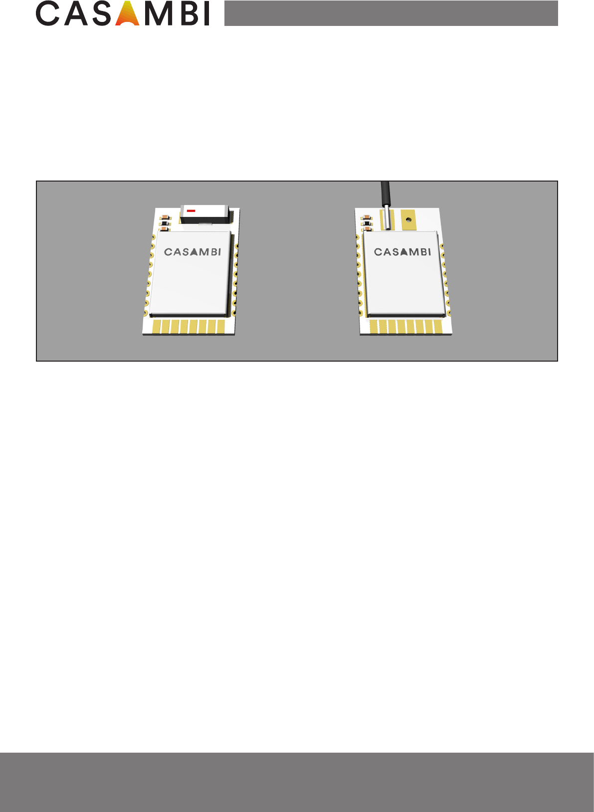
CBM-002A/B is available in two different antenna versions. CBM-002A is equipped with an on-board SMD
chip antenna and CBM-002B is equipped with a 1/4 wavelength dipole antenna. Usually CBM-002B offers
better range, but CBM-002A is more compact solution.
CBM-002B is delivered with the antenna detached, so the antenna will have to be soldered in place before
taking the module into use. This is because the antenna can be soldered in vertical or horizontal position. The
host device application determines which antenna orientation is more suitable. Read 14.5 CBM-002B Antenna
for more information.
14.3 Antenna Versions
Picture 7. CBM-002A on left and CBM-002B on right
www.casambi.com
info@casambi.com
tel. +358 10 501 2950
Casambi Technologies Oy
Linnoitustie 4 A
02600 Espoo, Finland
CBM-002A/B
Page 16 of 25
CBM-002A/B has two sets of soldering pads, which allow it to be mounted both in horizontal and vertical
position. In some application, such as LED drivers, there are large components which could affect the antenna
performance greatly if the module is mounted at the bottom of the device horizontally on the main PCB. Also,
horizontally mounted module has much larger footprint compared to vertically mounted module.
14.4 Mounting
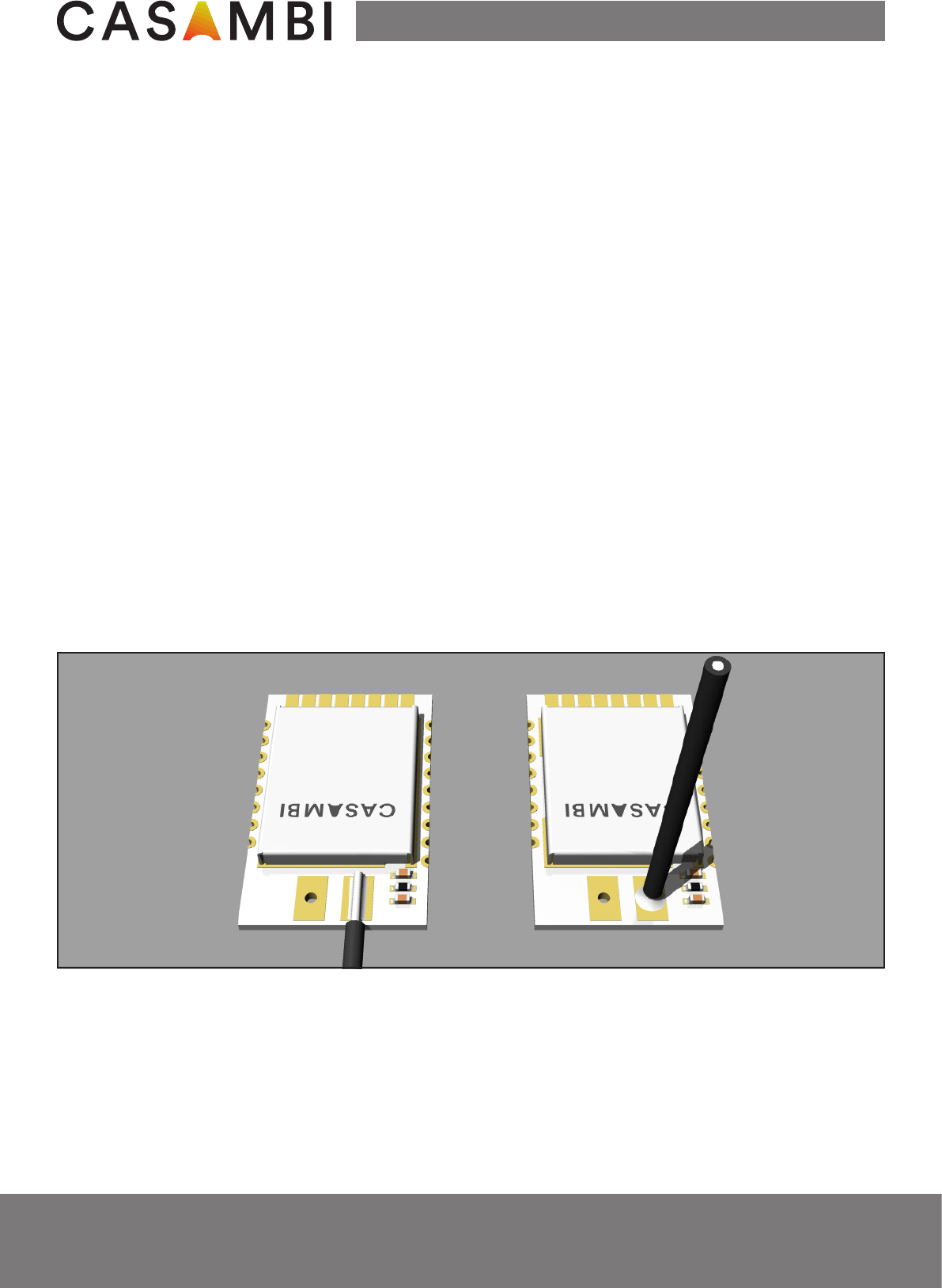
CBM-002B is delivered with the antenna detached. The antenna is a 27 mm long single strand copper wire
and it can be soldered in horizontal or vertical orientation, depending on the best suitability for the host ap-
plication.
The antenna can be bent to t the host application better. However, there are some guidelines that need to
be taken into consideration.
1. Make sure that antenna is not in contact with any kind of metal.
2. The antenna should be places as far away from any metal structures as possible.
3. The tip of the antenna is especially sensitive for close by metals.
4. The less bending is done on the antenna, the smaller impact it haves on the range.
4. Do not use any other kind of antenna, or do not cut or otherwise modify the delivered antenna.
The antenna is soldered onto the left side solder pad (the pad closer to the antenna matching components).
When soldering the antenna in horizontal position, for correct operation, place the antenna so that it lls the
whole length of the soldering pad. This way the antenna extents over the edge of the module by 23,5-24,0
mm.
When the antenna is soldered in vertical position, solder it so that the antenna rises 23,5-24,0 mm over the
PCB surface. Cut the antenna wire from the bottom side to the desired length. This cutting does not affect
the performance or approvals.
Important!
CBM-002B has been certied with the supplied antenna and modifying it beyond the instructions given in this
datasheet will void the certication.
14.3.1 CBM-002B Antenna
Picture 9. Soldered CBM-002B antennas.
www.casambi.com
info@casambi.com
tel. +358 10 501 2950
Casambi Technologies Oy
Linnoitustie 4 A
02600 Espoo, Finland
CBM-002A/B
Page 17 of 25
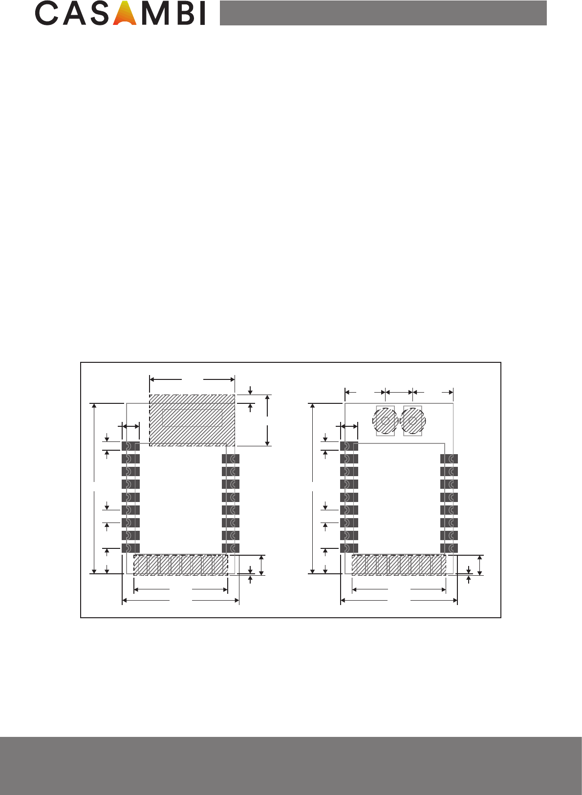
When CBM-002A/B is mounted in a horizontal position it is soldered in by using the soldering pads on both
long sides of the module. The soldering pads are designed so that the module can be both hand and reow
soldered.
When mounted in a horizontal position, there are two mandatory keep-out areas involved. One is for antenna
and the other is for bottom side soldering pads at the narrow end of the module. These pads are used for
vertical assembly.
For the CBM-002A, the antenna keep-out applies to all layers of the mother board. There shall not be any
components, traces, pads or copper areas in any layer within the keep-out area. The same applies to other
metals as well, such as the enclosure of the product, xing screws, etc.
The keep-out area for the soldering pads applies only to the outer surface of the mother board.
14.4.1 Horizontal Mounting
1) This keep-out area will have to be kept clear from any parts, traces and copper on all layers.
2) This keep-out area applies only to the layer closest to the module.
3) If CBM-002B antenna is soldered vertically, this keep-out area will have to be a hole. Otherwise keep-out
area applies only to the layer closest to the module.
Picture 9. Recommended land pattern for horizontal assembly and required keep-out areas
2)
11,00
2,40
2,00
1,00
1,50
3,00
20,00
13,70
0,20
1)
10,00
1,00 6,00
2)
11,00
2,40
2,00
1,00
1,50
3,00
20,00
13,70
0,20
4,75 4,75
3,20
2 x
2)3)
Ø3,00
CBM-002 CBM-002B
For such cases the module can be mounted in vertical position, either by soldering it to a 1,27 mm pitch 2-row
pin header, or by soldering the module directly into a routed slot on the main PCB.
When mounted in horizontal position there will have to be two keep-out areas; one for the antenna area and
one for the unused pads used for vertical assembly.
www.casambi.com
info@casambi.com
tel. +358 10 501 2950
Casambi Technologies Oy
Linnoitustie 4 A
02600 Espoo, Finland
CBM-002A/B
Page 18 of 25
CBM-002A/B can be mounted in vertical position by using the soldering pads on the narrow end of the mod-
ule. There are two methods of soldering the module in vertical position. It can be either soldered between pin
rows of a 2-row 1,27 mm pin header (2 x 8P) or it can be soldered in a 0,9 mm slot routed on the main board
with soldering pads at the edge of the slot. The thickness of the module printed circuit board is 0,85 mm.
14.4.2 Vertical Mounting
Pad size: 1 x 2 mm
1,27
12,7
0,90
Routed slot
Picture 11. Suggested land pattern for vertical mounting in a slot
15 Mechanical Specications
Picture 14. Mechanical dimensions
2,85
0,85 1,905
2,00
1,27 1,00 1,905 1,27 1,00
2,00
3,00
1,50
1,00
20,00
1,50
12,70
0,85 1,905
2,00
1,27 1,00 1,905 1,27 1,00
2,00
3,00
1,50
1,00
20,00
1,50
12,70
2,35 23,5-24,0
CBM-002A CBM-002B
www.casambi.com
info@casambi.com
tel. +358 10 501 2950
Casambi Technologies Oy
Linnoitustie 4 A
02600 Espoo, Finland
CBM-002A/B
Page 19 of 25
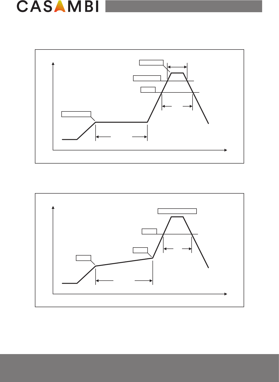
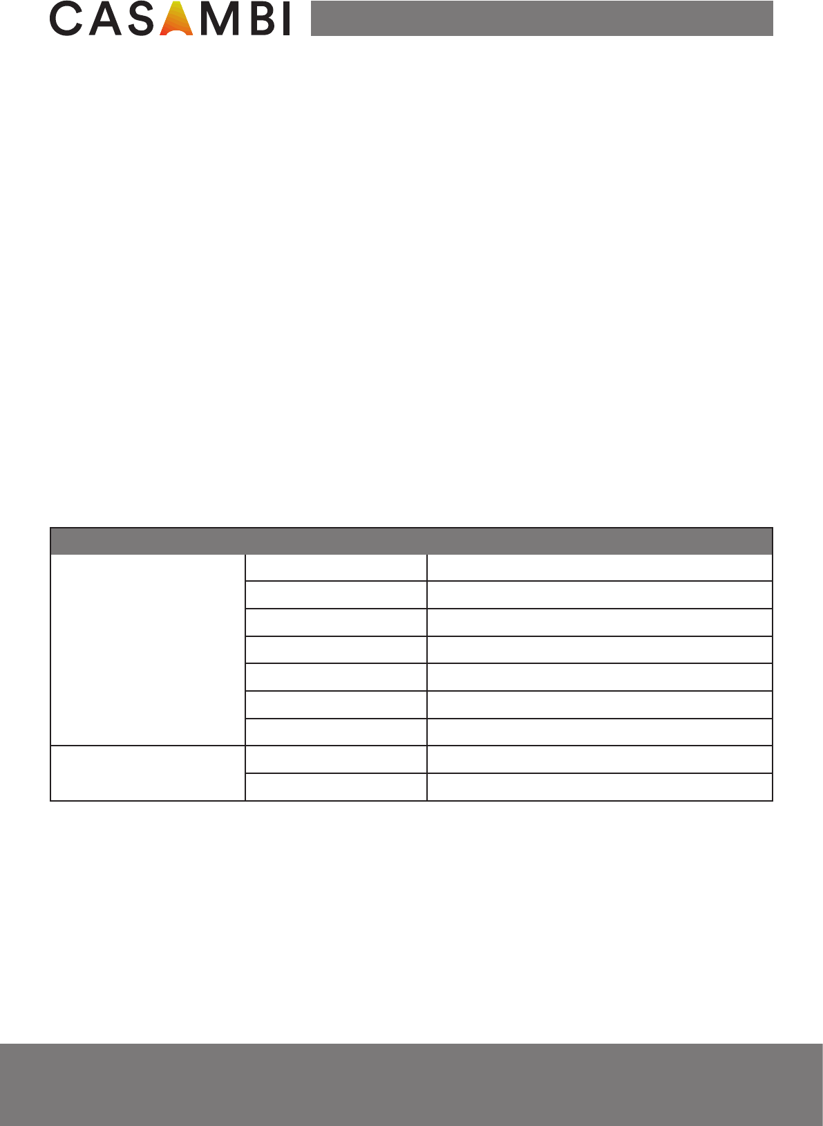
16.1 Leaded Reow Soldering
90s (±30s)
150˚C
190˚C
220˚C
30s
(+20s/-10s)
Max. 230˚C - 250˚C
Temp. (˚C)
Time (s)
Picture 13. Recommended temperature prole for leadfree reow soldering
90s (±30s)
150˚C (±10˚C)
30s
(+20s/-10s)
Temp. (˚C)
Time (s)
200˚C
220˚C (±5˚C)
10s (±1s)
Max. 235˚C
Picture 12. Recommended temperature prole for leaded reow soldering
Maximum number of reow cycles: 2
Opposite side reow is prohibited due to the module’s weight. (i.e. you must not place the module on the
bottom / underside of your PCB and reow).
16 Soldering
16.2 Leadfree Reow Soldering
www.casambi.com
info@casambi.com
tel. +358 10 501 2950
Casambi Technologies Oy
Linnoitustie 4 A
02600 Espoo, Finland
CBM-002A/B
Page 20 of 25
16.5 Cleaning
In general, cleaning the populated modules is strongly discouraged. Residuals under the module cannot be
easily removed with any cleaning process. Use of “No Clean” soldering paste is strongly recommended, as it
does not require cleaning after the soldering process.
16.3 Hand Soldering
Hand soldering is possible. When using a soldering iron, follow IPC recommendations (reference document
IPC-7711).
16.4 Rework
The module can be unsoldered from the host board. Use of a hot air rework tool should be programmable
and the solder joint and module should not exceed the maximum peak reow temperature of 250°C.
If temperature ramps exceed the reow temperature prole, module and component damage may occur due
to thermal shock. Avoid overheating. Never attempt a rework on the module itself, (e.g. replacing individual
components).
17 Compliance Information
Radio USA (not yet approved) FCC Part 15 Subpart C
Compliance Information
2ALA3-CBM002A
FCC ID (CBM-002B): 2ALA3-CBM002B
Europe ETSI EN 300 328 v2.1.1
RSS-247
22496-CBM002B
RoHS RoHS compilant
IC (CBM-002B):
REACH compilant
Environmental
REACH
Table 18. Compliance information
Canada (not yet appr.)
FCC ID (CBM-002A):
22496-CBM002AIC (CBM-002A):

www.casambi.com
info@casambi.com
tel. +358 10 501 2950
Casambi Technologies Oy
Linnoitustie 4 A
02600 Espoo, Finland
CBM-002A/B
Page 21 of 25
Compliance Statement
This device complies with part 15 of the FCC Rules. Operation is subject to the following two conditions:
(1) This device may not cause harmful interference, and
(2) this device must accept any interference received, including interference that may cause undesired opera-
tion.
Warning
Changes or modications not expressly approved by Casambi Technologies Oy could void the user’s author-
ity to operate the equipment.
FCC Interference Statement
This equipment has been tested and found to comply with the limits for a Class B digital device, pursuant to
Part 15 of the FCC Rules. These limits are designed to provide reasonable protection against harmful interfer-
ence in a residential installation.
This equipment generates, uses and can radiate radio frequency energy and, if not installed and used in ac-
cordance with the instructions, may cause harmful interference to radio communications.
However, there is no guarantee that interference will not occur in a particular installation. If this equipment
does cause harmful interference to radio or television reception, which can be determined by turning the
equipment off and on, the user is encouraged to try to correct the interference by one of the following meas-
ures:
• Reorient or relocate the receiving antenna.
• Increase the separation between the equipment and receiver.
• Connect the equipment into an outlet on a circuit different from that to which the receiver is connected.
• Consult the dealer or an experienced radio/TV technician for help.
It is the host manufacturer’s responsibility to ensure continued compliance with FCC requirements
once the module has been installed in to the host product.
17.1 Federal Communications Commission (FCC) Statement

www.casambi.com
info@casambi.com
tel. +358 10 501 2950
Casambi Technologies Oy
Linnoitustie 4 A
02600 Espoo, Finland
CBM-002A/B
Page 22 of 25
17.2 Innovation, Scientic and Economic Development Canada (ISED) Statement
Radiation Exposure Statement for Canada
This device complies with Industry Canada’s licence-exempt RSSs. Operation is subject to the following two
conditions:
(1) This device may not cause interference
(2) This device must accept any interference, including interference that may cause undesired operation of
the device.
This equipment is exempt from the routine RF exposure evaluation requirements of RSS-102. This equipment
should be installed and operated with a minimum distance of 20 cm between the antenna and the user or
bystanders.
Le présent appareil est conforme aux CNR d’Industrie Canada applicables aux appareils radio exempts de
licence. L’exploitation est autorisée aux deux conditions suivantes:
(1) l’appareil ne doit pas produire de brouillage;
(2) l’utilisateur de l’appareil doit accepter tout brouillage radioélectrique subi, même si le brouillage est sus-
ceptible d’en compromettre le fonctionnement.
Ce matériel n’est pas sujet à l’évaluation habituelle d’exposition RF selon RSS102. Ce matériel devrait être in-
stallé et exploité en gardant une distance minimale de 20 cm entre l’antenne et l’utilisateur ou les spectateurs.
Antenna Warning
CBM-002B radio transmitter has been approved by ISED to operate with the antenna types listed below with
the maximum permissible gain indicated. Antenna types not included in this list, having a gain greater than
the maximum gain indicated for that type, are strictly prohibited for use with this device.
L’émetteur radio CBM-002B est approuvé par les indicateurs du développement énergétique durable pour
fonctionner avec les types d’antennes énumérés ci-dessous avec la valeur maximale de gain autorisée indi-
quée. L’utilisation des types d’antennes exclus de cette liste, ayant un gain plus élevé que la valeur maximale
de gain indiquée pour le type en question, est strictement interdite avec cet appareil.
Approved antenna:
27 mm long solid copper wire with conductor diameter of 0,6 mm soldered in place according
to the instruction given in this document (see chapter 14.4.1 CBM-002B Antenna). Maximum
permissible antenna gain is 2,0 dBi.
Le l de cuivre 27 mm de long avec un diamètre conducteur de 0,6 mm soudé en place con-
formément aux instructions contenues dans ce document (voir chapitre 14.4.1 Antenne CBM-
002B). Valeur maximale permise pour gain d’antenne est de 2,0 dBi.
Under ISED regulations, this radio transmitter may only operate using an antenna of a type and maximum (or
lesser) gain approved for the transmitter by ISED. To reduce potential radio interference to other users, the
antenna type and its gain should be so chosen that the equivalent isotropically radiated power (e.i.r.p.) is not
more than that necessary for successful communication.
Sous les règlements des indicateurs du développement énergétique durable, cet émetteur radio peut seule-
ment fonctionner en utilisant un type d’antenne avec une valeur maximale (ou moindre) de gain approuvée
pour l’émetteur par les indicateurs du développement énergétique durable. An de réduire la possible inter-
férence radio avec les autres utilisateurs, le type d’antenne et son gain doivent être sélectionnés an que la
puissance isotrope rayonnée équivalente ne soit pas supérieure à ce qui est nécessaire pour une communica-
tion réussie.
www.casambi.com
info@casambi.com
tel. +358 10 501 2950
Casambi Technologies Oy
Linnoitustie 4 A
02600 Espoo, Finland
CBM-002A/B
End Product Labeling
CBM-002 has been labeled with its own FCC ID and IC Certication Number. The end product manufacturer
must ensure that FCC and ISED labeling requirements are met. If the FCC ID and IC Certication Number of
CBM-002 are not visible when the module is installed inside another device, then the device must have a
clearly visible label containing the following information:
CBM-002 a été identié avec son propre numéro d’identication de la FCC ainsi que son numéro de certica-
tion IC. Le fabricant du produit nal doit assurer que les obligations d’identication de la FCC et des indica-
teurs du développement énergétique durable soient satisfaites. Si le numéro d’identication de la FCC et le
numéro de certication IC pour CBM-002 ne sont pas visibles lors de l’installation du module dans un autre
appareil, une étiquette claire et visible avec les informations ci-après devra alors être apposée sur l’appareil:
Contains FCC ID: 2ALA3-CBM002A
Contains IC: 22496-CBM002A
Contains FCC ID: 2ALA3-CBM002B
Contains IC: 22496-CBM002B
CBM-002A:
CBM-002B:
Page 23 of 25
It is the host manufacturer’s responsibility to ensure continued compliance with ISED Canada requirements
once the module has been installed in to the host product.
It is the host manufacturer’s responsibility to ensure continued compliance with ISED Canada requirements
once the module has been installed in to the host product.
www.casambi.com
info@casambi.com
tel. +358 10 501 2950
Casambi Technologies Oy
Linnoitustie 4 A
02600 Espoo, Finland
CBM-002A/B
Page 24 of 25
This device complies with part 15 of the FCC Rules. Op-
eration is subject to the following two conditions:
(1) This device may not cause harmful interference, and
(2) this device must accept any interference received,
including interference that may cause undesired opera-
tion.
-------------------------------------------------------------
This device complies with Industry Canada’s license-
exempt RSSs. Operation is subject to the following two
conditions:
(1) This device may not cause interference; and
(2) This device must accept any interference, including
interference that may cause undesired operation of the
device.
Le présent appareil est conforme aux CNR d’Industrie
Canada applicables aux appareils radio exempts de li-
cence. L’exploitation est autorisée aux deux conditions
suivantes:
(1) l’appareil ne doit pas produire de brouillage;
(2) l’utilisateur de l’appareil doit accepter tout brouillage
radioélectrique subi, même si le brouillage est suscepti-
ble d’en compromettre le fonctionnement.
End Product User Manual
User manual for end product with CBM-002A or CBM-002B module inside shall contain the following or
equivalent notice in a conspicuous location in the user manual or alternatively on the device or both:
Le mode d’emploi pour le produit ni avec le module CBM-002A ou CBM-002B installé devra contenir les in-
formations ci-après ou un avis équivalent dans un endroit bien en vue du mode d’emploi ou, alternativement,
sur l’appareil, ou aux deux endroits:

www.casambi.com
info@casambi.com
tel. +358 10 501 2950
Casambi Technologies Oy
Linnoitustie 4 A
02600 Espoo, Finland
CBM-002A/B
17.3 CE Declaration of Conformity
Hereby, Casambi Technologies Oy declares that the radio equipment types CBM-002A and CBM-002B are in
compliance with Directive 2014/53/EU.
The full text of the EU declaration of conformity is available at the following internet address:
https://casambi.com/static/datasheets/CBM-002-DoC.pdf
CE Regulatory Information
When integrating a radio module into an end product the integrator becomes the manufacturer of the nal
product and is therefore responsible for demonstrating compliance of the nal product with the essential
requirements of the Radio Equipment Directive (RED).
Some additional certication processes are required before placing the product on the market in EU member
states to make the end product fully comply with relative EU standards.
© Casambi Technologies Oy, 2017. Data is subject to change without prior notice.
Page 25 of 25