Casio Electronic Keyboard Ctk 401 Users Manual S/M
ctk4014 4c79dd5b-d019-4175-b437-874d326cce01 Casio Electronic Keyboard CTK-401 User Guide |
2015-01-21
: Casio Casio-Casio-Electronic-Keyboard-Ctk-401-Users-Manual-243272 casio-casio-electronic-keyboard-ctk-401-users-manual-243272 casio pdf
Open the PDF directly: View PDF ![]() .
.
Page Count: 19
- ÿþ�C�T�K�-�4�0�1
- ÿþ�C�O�N�T�E�N�T�S
- ÿþ�S�P�E�C�I�F�I�C�A�T�I�O�N�S
- ÿþ�B�L�O�C�K� �D�I�A�G�R�A�M
- ÿþ�C�I�R�C�U�I�T� �D�E�S�C�R�I�P�T�I�O�N
- ÿþ�A�D�J�U�S�T�M�E�N�T
- ÿþ�M�A�J�O�R� �W�A�V�E�F�O�R�M�S
- ÿþ�P�R�I�N�T�E�D� �C�I�R�C�U�I�T� �B�O�A�R�D�S
- ÿþ�S�C�H�E�M�A�T�I�C� �D�I�A�G�R�A�M�S
- ÿþ�E�X�P�L�O�D�E�D� �V�I�E�W
- ÿþ�P�A�R�T�S� �L�I�S�T
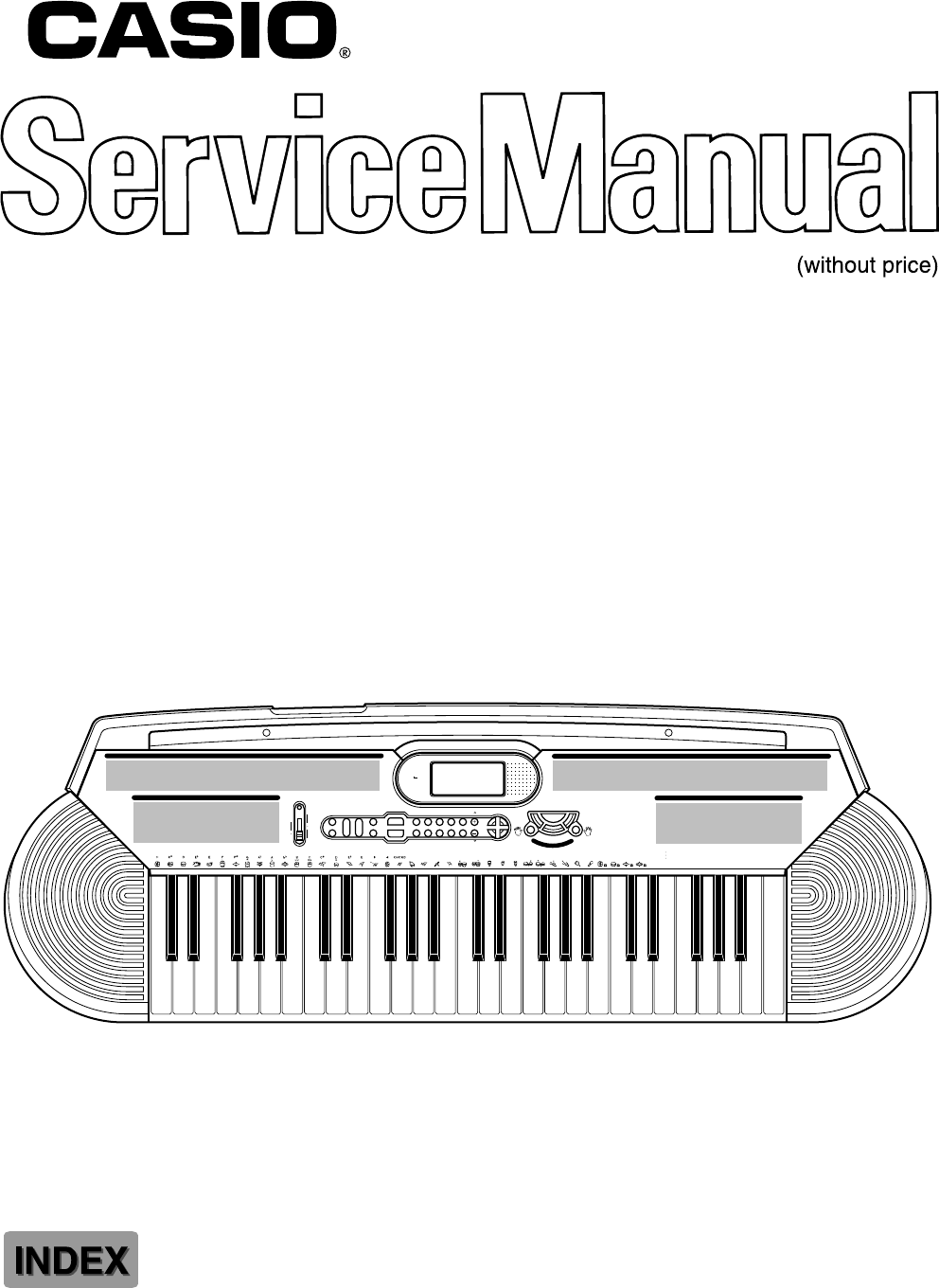
ELECTRONIC KEYBOARD
CTK-401
CTK-401
POWER/MODE
FINGERED
MAIN
VOLUMESYNCHRO/
FILL-IN START/
STOP TEMPO CHORD BOOK M
01234
56789
m 7 M7 dim
aug sus4 -5 add9 CLEAR
ACCOMP VOLUME
CASIO
CHORD
ON
OFF NORMAL
100 RHYTHMS
100 SONG BANK (00-49)
TONE SONG BANK REW STOP FF
100 SONG BANK KEYBOARD
MUSICAL INFORMATION SYSTEM
SONG BANK CONTROLLER
LEFT
ON/OFF
RIGHT
ON/OFF
PLAY/
PAUSE
TRANSPOSE/
TUNE
RHYTHM
S
O
N
G
B
A
N
K
C
O
N
T
R
O
L
L
E
R
100 TONES
100 SONG BANK (50-99)
TONE
RHYTHM
SONG BANK
MUSICAL INFORMATION SYSTEM
STATUS
TEMPO
VOLUME
CONTENTS
Specifications ................................................................................................................................... 1
Block Diagram.................................................................................................................................. 2
Circuit Description ............................................................................................................................ 3
Adjustment ....................................................................................................................................... 7
Major Waveforms ............................................................................................................................. 8
Printed Circuit Boards ...................................................................................................................... 9
Schematic Diagrams ...................................................................................................................... 11
Exploded View ............................................................................................................................... 15
Parts List ........................................................................................................................................ 17

— 1 —
SPECIFICATIONS
GENERAL
Keyboard: 49 standard-size keys, 4 octaves
Tones: 100
Polyphony: 12 notes maximum (6 for certain tones)
Auto accompaniment
Rhythm patterns: 100
Tempo: Variable (236 steps, = 20 to 255)
Chords: 2 fingering methods (CASIO CHORD, FINGERED)
Rhythm controller: START/STOP, SYNCHRO/FILL-IN
Accomp volume: 0 to 9 (10 steps)
Song bank
Tunes: 100
Controllers: PLAY/PAUSE, STOP, REW, FF, LEFT ON/OFF, RIGHT ON/OFF
Musical dictionary
Name display: TONE, RHYTHM, SONG BANK name/number
Tempo: Tempo value, metronome, synchro standby, beat indicator
Chord: Chord name, Chord form
Fingering: Fingering indcators, parts
Song bank status: PLAY, PAUSE, REW, FF, playing
Staff: Four octaves with sharp and flat indications
Keyboard: Four octaves
Other functions
Transpose: 12 steps (–6 semitones to +5 semitones)
Tuning: Variable (A4 = approximately 440 Hz ± 50 cents)
Volume: 0 to 9 (10 steps)
Terminals
Phones/Output terminal: Stereo standard jack
Output Impedance: 100 Ω
Output Voltage: 3.0 V (RMS) MAX
Power supply terminal: 9 V DC
Power supply Dual power supply system
Batteries: Six AA-size batteries
Battery life: Approximately 2 hours (SUM-3/R6P)/6 hours (AM3/LR6)
AC adaptor: AD-5
Auto power off: Turns power off approximately six minutes after last key operation. Enabled
under battery power only, can be disabled manually.
Speaker output: 2.0 W + 2.0 W
Power consumption: 9 V --- 7.0 W
Dimensions (HWD): 988 × 332 × 124 mm (38-15/16 × 13-1/16 × 4-7/8 inches)
Weight: Approximately 3.5 kg (7.7 lbs) (without batteries)
ELECTRICAL
Current drain with 9 V DC:
No sound output 100 mA ± 20 %
Maximum volume 625 mA ± 20 %
with 12 keys C4 to B4 pressed in Synth-Lead 1
Volume: 9 (Max.)
Phone output level (Vrms with 8 Ω load each channel):
with key A4 pressed in Synth-Lead 1 67 mV ± 20 %
Speaker output level (Vrms with 4 Ω load each channel):
with key A4 pressed in Synth-Lead 1 900 mV ± 20 %
Minimum operating voltage: 5.7 V
— 2 —
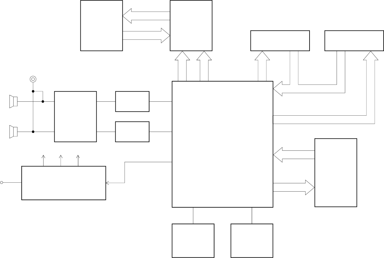
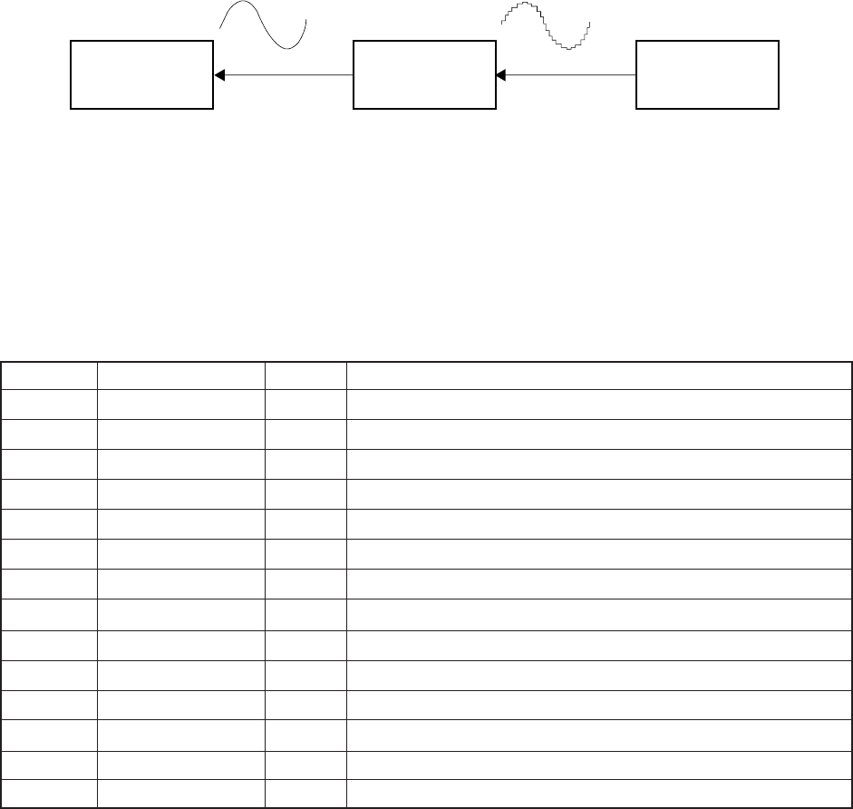
BLOCK DIAGRAM
CPU
MSM 6755B-17
LSI1
Keyboard
Buttons
LCD LCD Driver
SED1278F0A
LSI3
Reset IC
IC1 Oscillator
X1, Q1
Power Supply Circuit
Q101 ~ Q103, D104
Power Amp.
TA8248K
IC101
Filter (L)
Q104
Filter (R)
Q105
Output
VC VCC DVDD
APO
MD0 ~ MD7
MA0 ~ MA17
DC + 9 V IN
DB4 ~ DB7
COM1 ~ COM16
SEG1 ~ SEG40
RS
R/W
EKO8 ~
KO12 KI0 ~ KI6
KO0 ~ KO7
ROM(2M-bit)
UM23C2101M
7384/Q
LSI2
— 3 —
CIRCUIT DESCRIPTION
KEY MATRIX
NOMENCLATURE OF KEYS
KI0 KI1 KI2 KI3 KI4 KI5 KI6
KO0 C2 G#2 E3 C4 G#4 E5 C6
KO1 C#2 A2 F3 C#4 A4 F5
KO2 D2 A#2 F#3 D4 A#4 F#5
KO3 D#2 B2 G3 D#4 B4 G5
KO4 E2 C3 G#3 E4 C5 G#5
KO5 F2 C#3 A3 F4 C#5 A5
KO6 F#2 D3 A#3 F#4 D5 A#5
KO7 G2 D#3 B3 G4 D#5 B5
KO8 —+ 0
Tempo
Down Tempo
Up Volume
Down Volume
Up
KO9 321
Start/
Stop Synchro/
Fill-in Chord
Book Accomp
Volume
KO10 654
Transpose/
Tune Song
Bank Rhythm Tone
KO11 9 8 7 Fingered CASIO
Chord Normal Power Off
KO12 FF Right Play/
Pause Stop Left Rewind
C2
C#2 D#2 F#2 G#2 A#2 C#3 D#3 F#3 G#3 A#3 C#4 D#4 F#4 G#4 A#4 C#5 D#5 F#5 G#5 A#5
D2 E2 F2 G2 A2 B2 C3 D3 E3 F3 G3 A3 B3 C4 D4 E4 F4 G4 A4 B4 C5 D5 E5 F5 G5 A5 B5 C6

— 4 —
CPU (LSI1: MSM6755B-17)
The CPU reads sound data from the ROM in accordance with the pressed key and the selected tone; the CPU
can read rhythm data simultaneously when a rhythm pattern is selected. Then it provides the left and the right
channels’ waveforms separately, by converting the data into the waveforms with two built-in DACs. The CPU
also controls key and button input. The following table shows the pin functions of LSI1.
Pin No. Terminal In/Out Function
1 MA14 Out Address bus
2, 3 NCO — Not used
4 ~ 19 MA0 ~ MA13 Out Address bus
13 MRDB Out Read enable signal
17 MCSB — Not used
20 ~ 27 MD0 ~ MD7 In/Out Data bus
28, 29 NC1, NC2 — Not used
30 DGND In Ground (0 V) source
31 DVCC In +5 V source
32, 33 XTLO, XTLI In/Out 20 MHz clock input/output
34 NC3 — Not used
35 RSTB In Reset signal input
36 P24/RXD — Not used. Connected to +5 V.
37 P25/TXD — Not used
38 NMI In Power ON signal input. Connected to +5 V.
39 APO Out APO (Auto Power Off) signal output
40 NC4 — Not used
41 REFH Out Terminal for the internal DAC
42, 43 NC5, NC6 — Not used
44 DAOR Out Right channel sound waveform output
45 NC7 — Not used
46 AVdac In +5 V source for the internal DAC
47 DAOL Out Left channel sound waveform output
48 REFL Out Terminal for the internal DAC and ADC
49 AGdac In Ground source for internal DAC
50 AGadc In Ground source for internal ADC
51 ANI In APO cancellation signal
52 AVadc In +5 V source for the internal ADC
53 NC8 — Not used
54 MOD0 In Mode selection terminal. Connected to +5 V.
55, 56 MOD1, MOD2 In Mode selection terminal. Connected to ground.
57 P40 — Not used
58 ~ 64 KI0/P30 ~ KI7/P36 In Terminals for key/button input signal
65 KI7/P37 — Not used
66 ~ 73 KO0/P50 ~ KO7/P57 Out Terminals for key scan signal
— 5 —
LCD DRIVER (LSI3: SED1278F0A)
The LCD driver can drive a dot matrix LCD having 40 segment and 16 common lines. The LSI contains 240
graphic symbols in the built-in character generator ROM, and stores 80 characters in the built-in display data
RAM. In accordance with command from the CPU, the LSI is capable of displaying up to 16 characters
simultaneously. The following table shows the pin functions of LSI3.
Pin No. Terminal In/Out Function
74 ~ 77 DB4 ~ DB7 Out Data bus for the LCD driver
78 NC9 — Not used
79 LVCC In +5 V source
80 ~ 84 KO8 ~ KO12 Out Terminals for button scan signal
85 ~ 87 P65 ~ P67 — Not used
88 RS Out Control signal for the LCD driver
89 R/W Out Read/Write signal for the LCD driver
90 E Out Chip enable signal for the LCD driver
91 ~ 95 P73 ~ P77 — Not used
96 LGND In Ground source
97, 100 MA18, MA15 Out Address bus
Pin No. Terminal In/Out Function
1 ~ 22,
63 ~ 80
23 VSS — GND (0 V) source
Terminals for the built-in clock pulse generator. The external
resistor connected determines the oscillation frequency.
LCD drive voltage input.
26 ~ 30 V1 ~ V5 In Those voltages are used for generating the stepped pulse of
the LCD drive signals.
31, 32 LP, XCLS — Not used
33 VDD In DVDD (+5 V) source
34, 35 FR, DO — Not used
Data/command determination terminal.
High: data, Low: command
37 R/W In Read/Write terminal. High: read, Low: write
Chip enable signal.
38 E In High: enable, the writing is done at fall edge.
Low: disenable
39 ~ 42 DB0 ~ DB3 — Not used. Connected to GND (0 V)
43 ~ 46 DB4 ~ DB7 In/Out Data bus
47 ~ 62 COM1 ~ COM16 Out Common signal/output
SEG1 ~ SEG40 Out Segment signal output
24, 25 OSC1, OSC2 In/Out
36 RS In
— 6 —
FILTER BLOCK
Since the sound signals from the CPU is stepped waveforms, the filter block is added to smooth the waveforms.
POWER AMPLIFIER (IC101: TA8248K)
The power amplifier is a two-channel amplifier with standby switch.
The following table shows the pin function of IC101.
Pin No. Terminal In/Out Function
1 NC — Not used
2 B.S.2 — Terminal for a bootstrap capacitor
3 OUT2 Out Channel 2 output
4 VCC In +9 V source
5 OUT1 Out Channel 1 output
6 B.S.1 — Terminal for a bootstrap capacitor
7 Power GND In Ground (0 V) source
8 Stand by In Power control signal input. 0 V: Off, +9 V: On
9 DC — Terminal for a decoupling capacitor
10 NF1 In Negative feedback input
11 IN1 In Channel 1 input
12 IN2 In Channel 2 input
13 NF2 In Negative feedback input
14, 15 Pre GND In Ground (0 V) source
Amp.
TA8248K Filter
Block CPU
MSM6755B-17
— 7 —
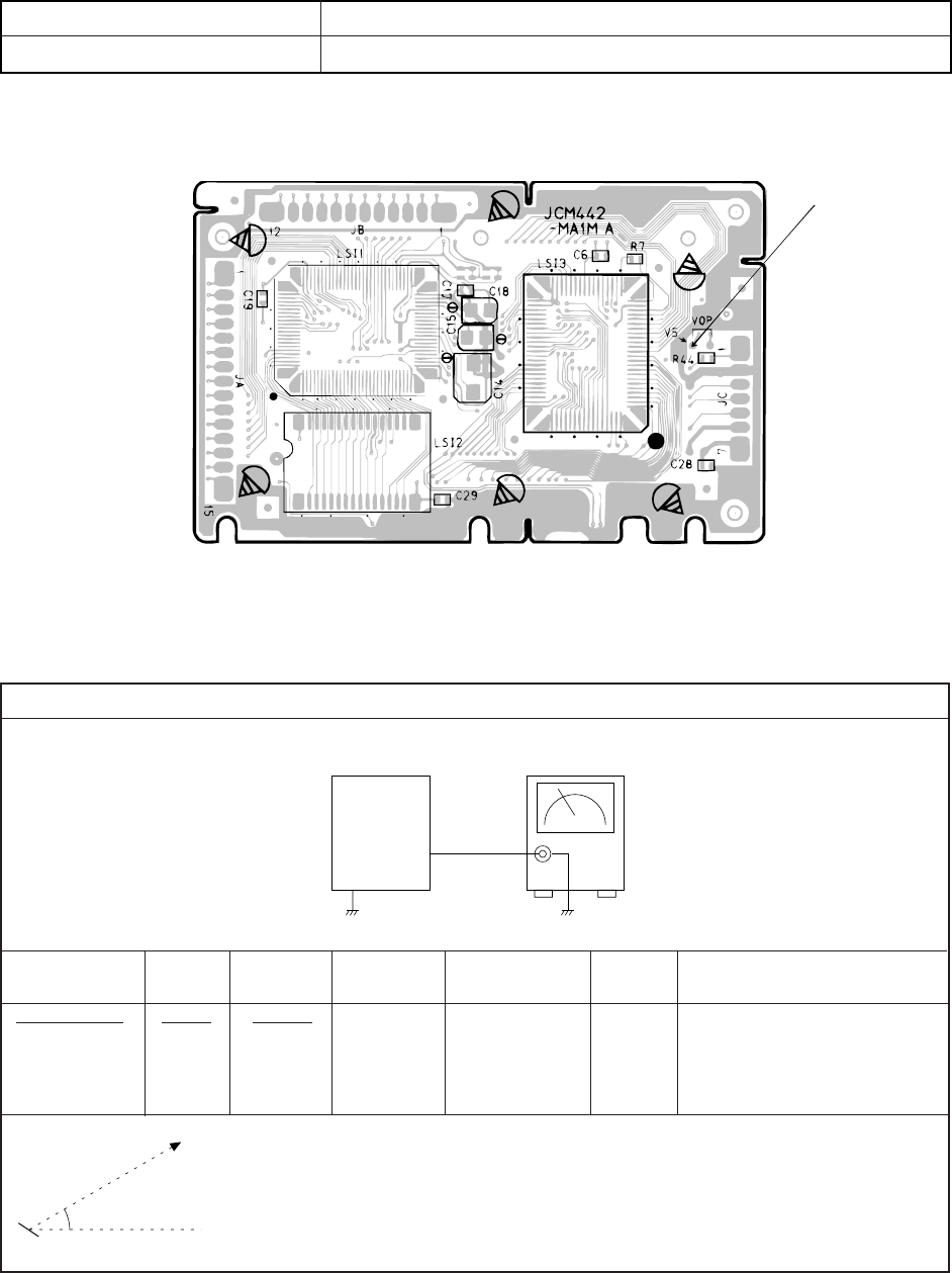
3) Equipment connection/Procedure
Vop voltage setting
Input
Connection Input
Point Input
Signal Adjust Output
Connection Output
Point Adjust for
VR1 Voltmeter V5 Adjust for 4.3 ±0.1 V reading
on voltmeter.
Make fine adjustment accord-
ing to the next instruction.
53.5°
LCD
Eye
Watching the LCD at a 53.5° angle to the horizontal, adjust Vop
voltage so that unenergized segments are seen dimly.
ADJUSTMENT
MAIN PCB
1) Items to be adjusted:
2) Adjustment and Test Point Locations
(TOP VIEW)
Item Measuring Instrument
Vop voltage setting Voltmeter
Test point
Output
Set Voltmeter
V5
— 8 —
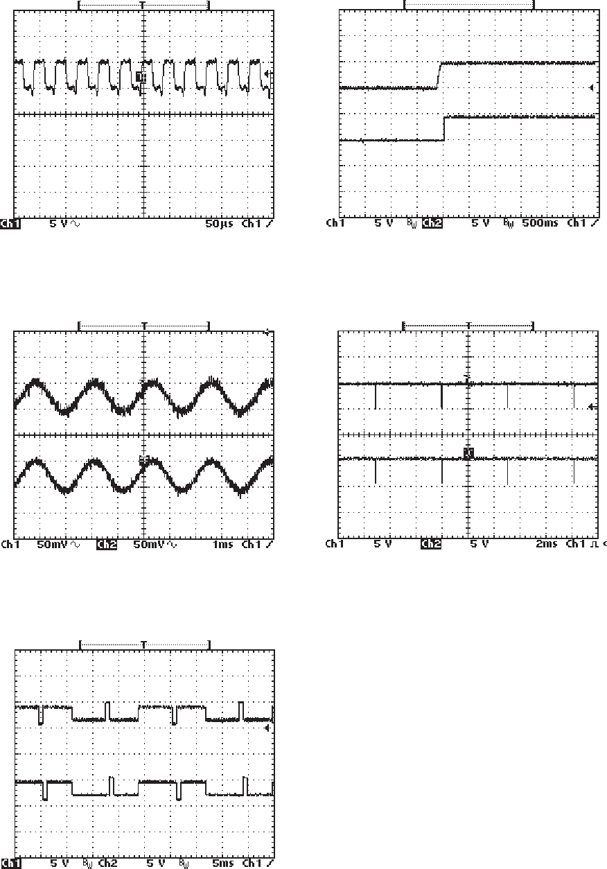
MAJOR WAVEFORMS
1Clock pulse
MSM6755B-17 pin 32
1
2+5 V source DVDD
JC connector pin 6
3APO signal
JC connector pin 5
2
3
4Sound waveform (R-ch) Tone: Whistle
JC connector pin 4 Key: A4
5Sound waveform (L-ch) Volume:
JC connector pin 3
4
5
6Button scan signal KO6
JA connector pin 14
7Button scan signal KO7
JA connector pin 15
6
7
8LCD common signal COM9
SED1278F0A pin 55
9LCD common signal COM10
SED1278F0A pin 56
8
9
— 9 —
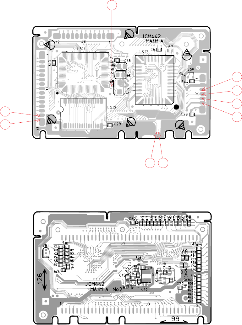
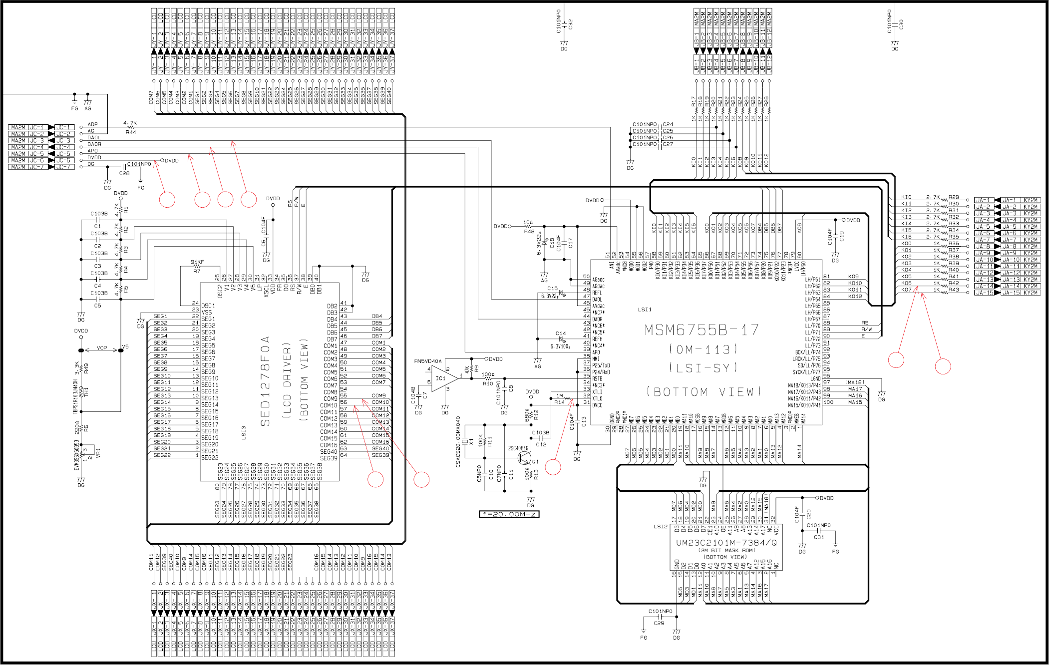
PRINTED CIRCUIT BOARDS
Main PCB JCM442-MA1M
Top View
Bottom View
1
2
3
4
5
89
6
7
— 11 —
SCHEMATIC DIAGRAMS
Main PCB JCM442-MA1M
67
1
98
5
4
32
— 12 —
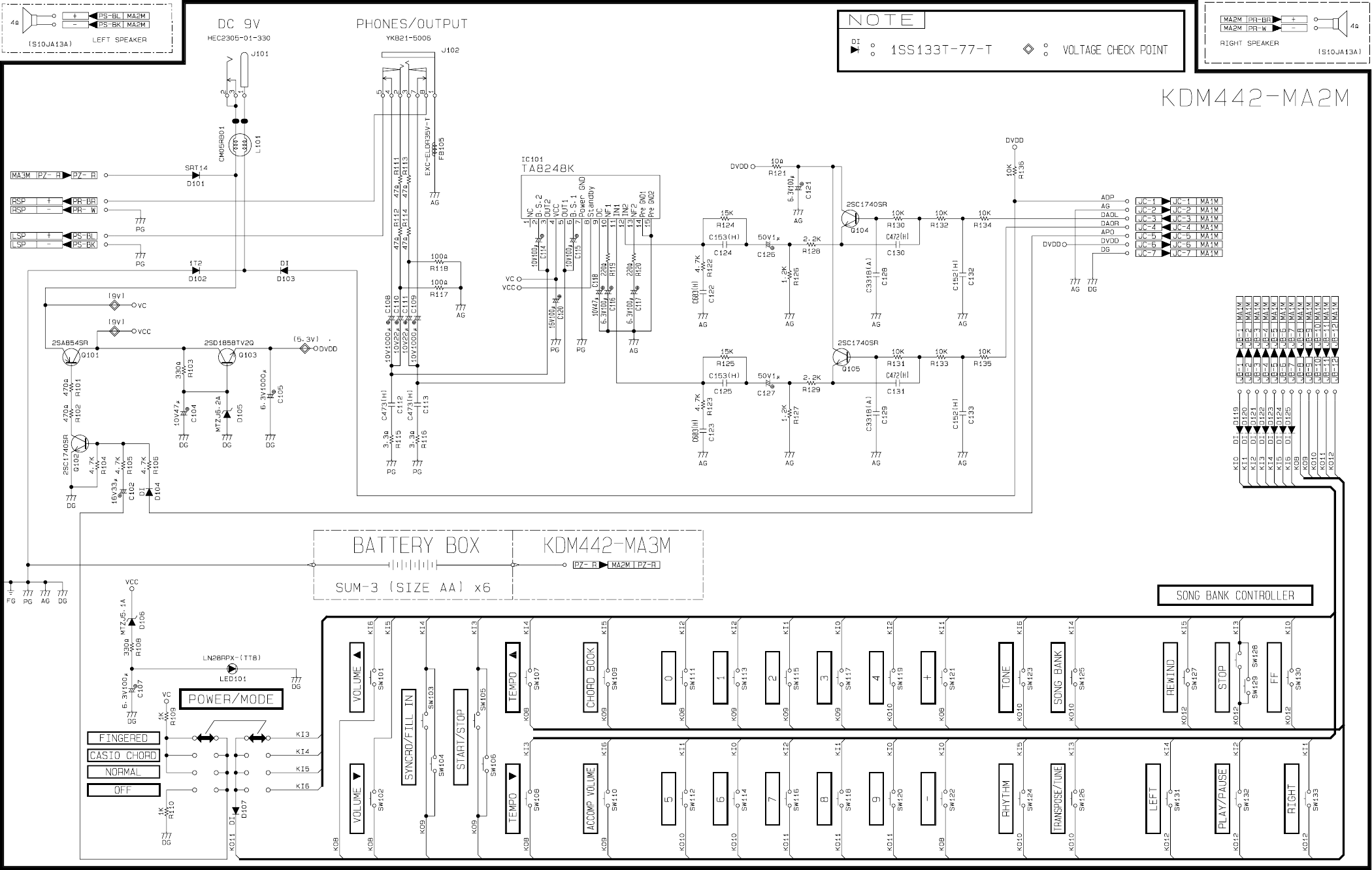
Sub PCB JCM442-MA2M
— 13 —
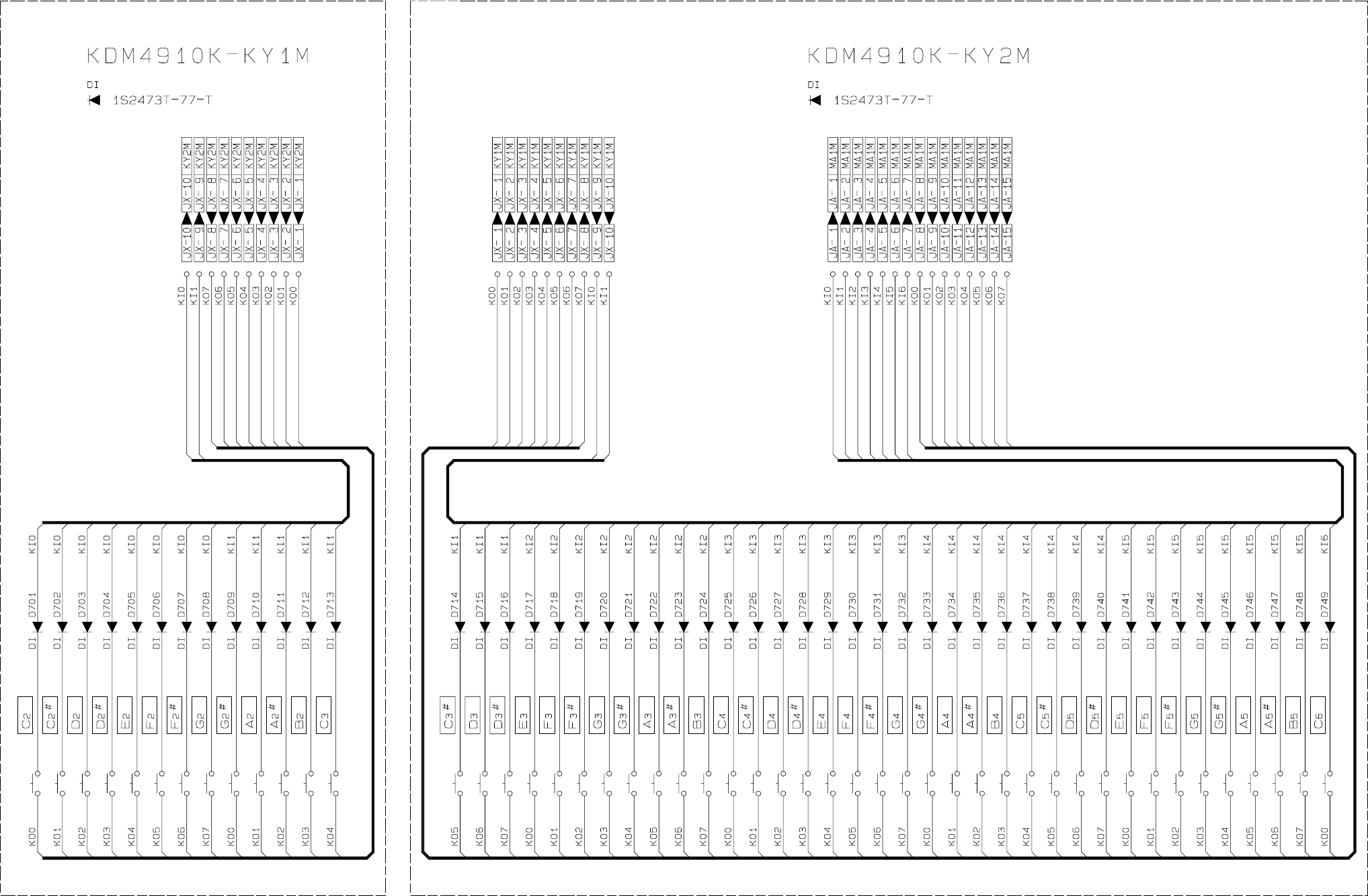
Keyboard PCBs KDM4910K-KY1M/KY2M
— 14 —
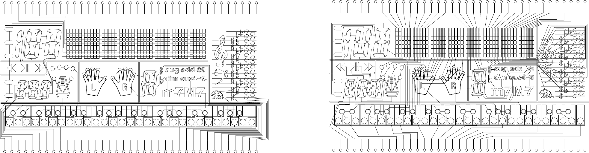
LCD
Segment
COM7
COM6
COM5
COM4
COM3
COM2
COM1
SEG2
COM11
COM12
SEG39
SEG40
COM10
COM9
COM14
COM15
COM16
SEG11
NC
NC
NC
COM16
SEG3
SEG4
SEG5
SEG6
SEG7
SEG8
SEG9
SEG10
SEG21
SEG22
SEG23
SEG24
SEG25
SEG26
SEG27
SEG28
SEG29
SEG30
SEG31
SEG32
SEG33
SEG34
SEG35
SEG36
SEG37
SEG38
SEG39
SEG40
SEG1
SEG12
SEG13
SEG14
SEG15
SEG16
SEG17
SEG18
SEG19
SEG20
SEG21
SEG22
SEG23
COM15
COM14
COM13
COM12
COM11
COM10
COM9
COM16
COM15
COM14
COM13
Common
— 15 —
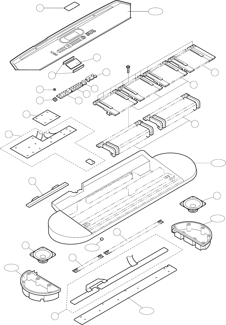
EXPLODED VIEW
18
14
13
15
12
11
19
17
16
10
R-1
R-2
R-3
5
6
8
79
4
R-4
R-6
R-5
4
3
1
2

Notes: This parts list does not include the cosmetic parts, which
parts are marked with item No. "R-X" in the exploded
view.
Contact our spare parts department if you need these
parts for refurbish.
1. Prices and specifications are subject to change with-
out prior notice.
2. As for spare parts order and supply, refer to the
"GUIDEBOOK for Spare parts Supply", published
seperately.
3. The numbers in item column correspond to the same
numbers in drawing.
PARTS LIST
CTK-401
Item Code No. Parts Name Specification Q R
Main PCB
1 6926 0200 PCB/ASS'Y (MA1M) M240592*1 1 B
LSI1 2012 5603 LSI/MC (CPU) MSM6755B-17 1 A
LSI2 2012 5611 LSI/MASK-ROM UM23C2101M-7384/Q 1 A
LSI3 2012 5569 LSI/LCD DRIVER SED1278F0A 1 A
IC1 2012 1883 IC/MOS (RESET IC) RN5VD40AA-TR 1 B
Q1 2252 1239 TRANSISTOR 2SC4081T106Q 1 B
VR1 2775 3286 POTENTIOMETER EVM3SSX50B53 1 B
X1 2590 2100 OSCILLATOR/CERAMIC CSACS20.00MX040-TC 1 B
Sub PCB
2 6926 0190 PCB/ASS'Y (MA2, 3M) M140548*1 1 B
IC101 2114 5775 IC/LINEAR (POWER AMP.) TA8248K 1 A
Q101 2250 0168 TRANSISTOR 2SA854SR-TP-T 1 A
Q102, Q104/105 2220 1409 TRANSISTOR 2SC1740SR-TP-T 3 A
Q103 2250 1585 TRANSISTOR 2SD1858TV2Q 1 A
D101 2390 1323 DIODE/SHOTTKY RB100A-T32-T 1 C
D102 2390 3018 DIODE 1T2 1 C
D103 2390 1344 DIODE 1SS133T-77-T 11 C
D104 2360 2044 DIODE/ZENER MTZJ6.2A-T77-T 1 A
D105 2360 1799 DIODE/ZENER MTZJ5.1A-T77-T 1 A
LED101 2370 0112 LED LN28RPX-(TT8) 1 C
J101 3501 7049 JACK (POWER) HEC2305-01-330 1 B
J102 3612 0665 JACK (PHONE) YKB21-5006 1 B
Keyboard PCBs
3 6926 0180 PCB/ASS'Y M140449*3 1 C
D701 - D749 2301 0101 DIODE 1S2473T-77-T 49 B
Mechanical Parts
4 3831 0770 SPEAKER S10JA13A 1 B
5 3335 6556 LCD LD-B10023A 1 B
6 6926 0270 RUBBER/INTERCONNECTOR M440435-2 2 C
7 6909 5890 SWITCH/SLIDE KONB CSB-12D 1 B
8 6921 5031 KNOB M311859-1 1 B
9 6926 0280 RUBBER/BUTTON M240587-1 1 B
10 6926 0290 RUBBER/BUTTON M240588-1 1 B
11 6926 0300 RUBBER/BUTTON M240589-1 1 B
12 6926 0310 RUBBER/BUTTON M240590-1 1 B
13 6922 2720 KEY SET/LT WHITE M312118*1 3 A
14 6922 2730 KEY SET/LT WHITE M312118*2 1A
15 6922 2740 KEY SET/LT BLACK 10P M111726-1 2 A
16 6922 4000 RUBBER/CONTACT M111765-1 1 A
17 6923 2390 RUBBER/CONTACT M240025-1 1 A
18 6926 0320 PANEL/DISPLAY M340608-1 1 C
19 6926 0020 COVER/BATTERY M340528*2 1 B
Accessory
6906 8752 STAND/NOTE M340629B*2 1 B
Notes: Q – Quantity per unit
R – Rank
— 17 —

MA0600571A
