Casio Electronic Keyboard Ctk 750 Users Manual S/M
CTK-750 to the manual 2b454f62-8c0d-4903-aa66-4c9ab1097b00
2015-01-21
: Casio Casio-Casio-Electronic-Keyboard-Ctk-750-Users-Manual-243279 casio-casio-electronic-keyboard-ctk-750-users-manual-243279 casio pdf
Open the PDF directly: View PDF ![]() .
.
Page Count: 30
- ÿþ�C�T�K�-�7�5�0
- ÿþ�C�O�N�T�E�N�T�S
- ÿþ�S�P�E�C�I�F�I�C�A�T�I�O�N�S
- ÿþ�R�E�P�L�A�C�I�N�G� �T�H�E� �D�S�P� �(�H�G�5�1�A�1�1�5�A�0�1�F�D�)
- ÿþ�B�L�O�C�K� �D�I�A�G�R�A�M
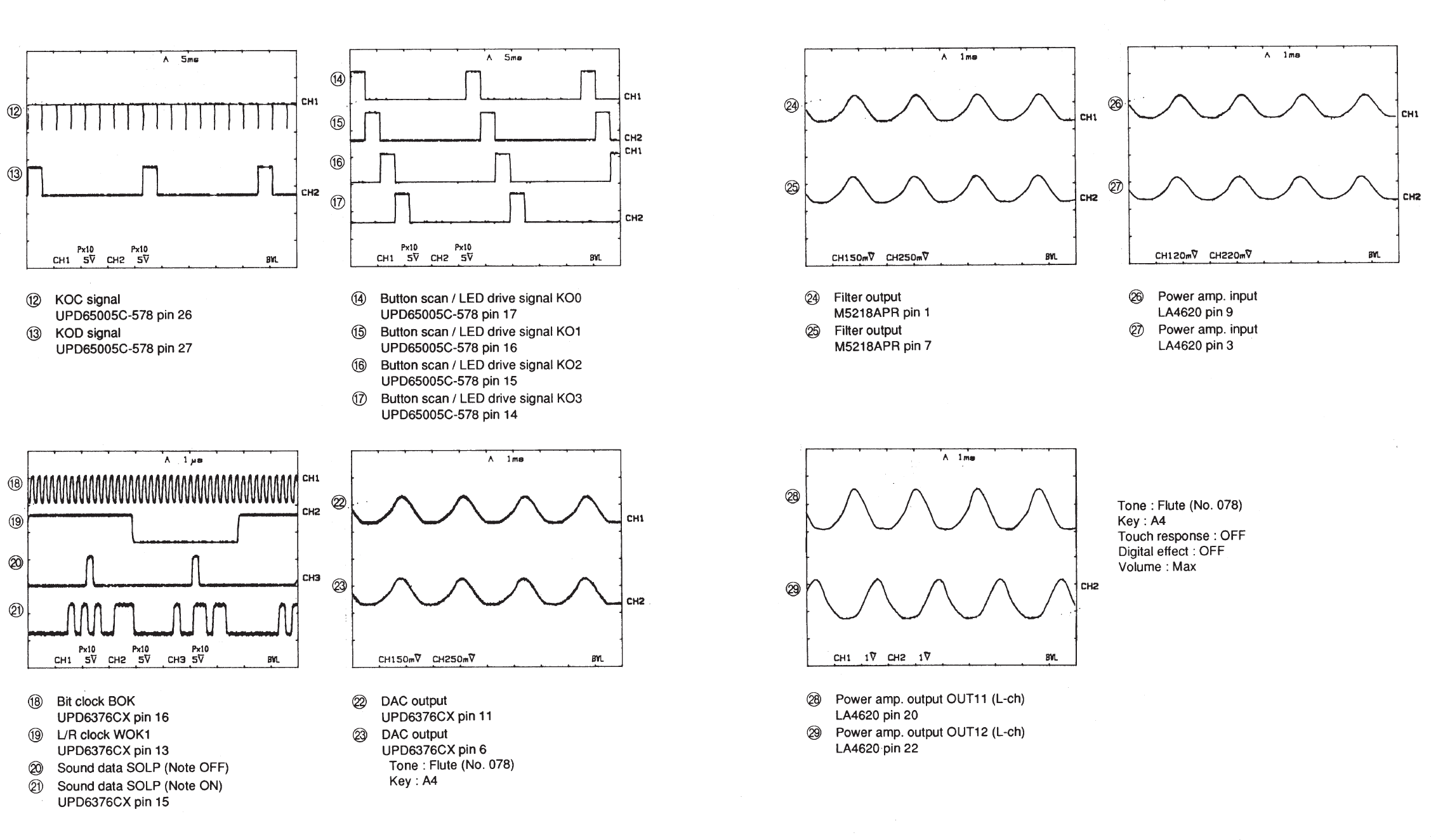
- ÿþ�C�I�R�C�U�I�T� �D�E�S�C�R�I�P�T�I�O�N
- ÿþ�K�e�y� �M�a�t�r�i�x
- ÿþ�N�o�m�e�n�c�l�a�t�u�r�e� �o�f� �K�e�y�s
- ÿþ�B�u�t�t�o�n� �M�a�t�r�i�x
- ÿþ�R�e�s�e�t� �C�i�r�c�u�i�t
- ÿþ�C�P�U� �(�H�D�6�4�3�3�2�9�8�A�1�8�P�)
- ÿþ�G�a�t�e� �A�r�r�a�y� �(�U�P�D�6�5�0�0�5�C�-�5�7�8�)
- ÿþ�D�i�g�i�t�a�l� �S�i�g�n�a�l� �P�r�o�c�e�s�s�o�r� �(�H�G�5�1�A�1�1�5�A�0�1�F�D�)
- ÿþ�B�l�o�c�k� �d�i�a�g�r�a�m� �o�f� �D�S�P� �a�n�d� �D�A�C� �c�i�r�c�u�i�t
- ÿþ�D�A�C� �(�U�P�D�6�3�7�6�C�X�)
- ÿþ�K�e�y� �T�o�u�c�h� �L�S�I� �(�H�G�5�2�E�3�5�P�)
- ÿþ�F�i�l�t�e�r� �B�l�o�c�k
- ÿþ�P�o�w�e�r� �A�m�p�l�i�f�i�e�r� �(�L�A�4�6�2�0�)
- ÿþ�P�o�w�e�r� �S�u�p�p�l�y� �C�i�r�c�u�i�t
- ÿþ�W�I�R�I�N�G� �D�I�A�G�R�A�M
- ÿþ�M�A�J�O�R� �W�A�V�E�F�O�R�M�S
- ÿþ�P�C�B� �V�I�E�W� �a�n�d� �M�A�J�O�R� �C�H�E�C�K� �P�O�I�N�T�S
- ÿþ�S�C�H�E�M�A�T�I�C� �D�I�A�G�R�A�M�S
- ÿþ�E�X�P�L�O�D�E�D� �V�I�E�W
- ÿþ�I�C� �L�E�A�D� �I�D�E�N�T�I�F�I�C�A�T�I�O�N� �A�N�D� �I�N�T�E�R�N�A�L� �D�I�A�G�R�A�M
- ÿþ�P�A�R�T�S� �L�I�S�T
(with price)
CTK-750
ELECTRONIC KEYBOARD
R
CTK-750

— 14 —
CONTENTS
Specifications . . . . . . . . . . . . . . . . . . . . . . . . . . . . . . . . . . . . . . . . . . 1
Replacing the DSP (HG51A115A01FD) . . . . . . . . . . . . . . . . . . . . . 2
Block Diagram . . . . . . . . . . . . . . . . . . . . . . . . . . . . . . . . . . . . . . . . . 3
Circuit Description . . . . . . . . . . . . . . . . . . . . . . . . . . . . . . . . . . . . . 4
Wiring Diagram . . . . . . . . . . . . . . . . . . . . . . . . . . . . . . . . . . . . . . . 13
Major Waveforms . . . . . . . . . . . . . . . . . . . . . . . . . . . . . . . . . . . . . . 14
PCB View and Major Check Points . . . . . . . . . . . . . . . . . . . . . . . 16
Schematic Diagrams . . . . . . . . . . . . . . . . . . . . . . . . . . . . . . . . . . 17
Exploded View . . . . . . . . . . . . . . . . . . . . . . . . . . . . . . . . . . . . . . . . 20
IC and Transistor Lead Identification . . . . . . . . . . . . . . . . . . . . . 21
Parts List . . . . . . . . . . . . . . . . . . . . . . . . . . . . . . . . . . . . . . . . . . . 23
— 1 —
General
Number of Keys: 61
Polyphonic: 32-note
Preset Tones: 128
Tone Expander: Layer, Split
Keyboard Controls: Touch Response: On/Off
Touch Sensitivity: Light/Middle/Heavy
Key Transpose: Range from F# to F by a half-note increment
Auto-Rhythms: 128
Tempo Control: 40 to 255
Auto-Accompaniment: CASIO Chord/Fingered/Full-Range Chord
Controller: Variation, Fill-In, Intro/Ending
Magical Preset Variations: 128; BREAK BEAT 16 MELODYCOMP 8
SHADOW DRUM 4 FREE SESSION 32
TONE STACK 40 KEY SPLIT 12
HYPERACTIVE 16
Digital Effects: 16; Reverb-1, Reverb-2, Reverb-3, Chorus, Tremplp, Phase Shifter,
Organ SP, Enhancer, Flanger, EQ Loudness, Delay-1, Delay-2,
Analog Delay, Tap Delay, Chorus Reverb, Tremolo Reverb
Sound/Control Pads: 6
Pad Variations: 32; Phrases: 10, Drums: 10, SE/Percussion: 10, Controller: 2
Song Memories: 2; Tracks: 6
System: Real-time recording
Memory Capacity: Approx. 5,800 notes
Registration Memories: 10
Registration Items: Tone Number, Rhythm Number, Tempo, Accompaniment Mode,
Accompaniment Volume, Effects, Layer On/Off, Split On/Off,
Pad Variation, Assignable Jack, Auto-Accompaniment On/Off,
Auto-Accompaniment Controller, MIDI (Channel On/Off, GM On/Off,
Local Control On/Off, Bend Range)
Tuning Control: 440Hz ± 100 cents
Terminals: Headphone Jack [Output Impedance: 100 Ω, Output Voltage: 1.7 V(rms)
MAX], Assignable Jack, MIDI Jacks (IN, OUT), AC Adaptor Jack (12V)
Built-In Speakers: 12 cm dia. 1.1W Input Rating: 2 pcs.
Power Source: 2-way AC or DC source
AC: AC adaptor AD-12
DC: 6 D size dry batteries
Battery life: Approx. 5 hours by manganese batteries R20P(SUM-1)
Approx. 5 hours by alkaline batteries LR20(AM1)
Auto Power Off: Approximately 6 minutes after the last operation
Power Consumption: 18 W
Dimentions: 141 x 968 x 411 mm (HWD)
(5-11/16 x 38-1/16 x 16-5/16 inches) (HWD)
Weight: 7.0 kg (15.5 lbs) excluding batteries
Standard Accessory: Music stand
SPECIFICATIONS
— 2 —
Electrical
Current Drain with 12V DC:
No Sound Output 390 mA ± 20%
Maximum Volume 1700 mA ± 20%
with white keys D2 to D3 pressed in Synth-Bass-2 tone
and in Latin Fusion rhythm at initial setup tempo
Volume; maximum, Touch: maximum
Line Output Level (Vrms with 47 KΩ load each cannel):
with key D4 pressed in FSynth-Bass-2 tone on L-ch 850 mV ± 20%
with key G4 pressed in FSynth-Bass-2 tone on R-ch 800 mV ± 20%
Phone Output Level (Vrms with 8 Ω load each channel):
with key D4 pressed in FSynth-Bass-2 tone on L-ch 280 mV ± 20%
with key G4 pressed in FSynth-Bass-2 tone on R-ch 260 mV ± 20%
Speaker Input Level:
with key D4 pressed in FSynth-Bass-2 tone on L-ch 5200 mV ± 20%
with key G4 pressed in FSynth-Bass-2 tone on R-ch 5600 mV ± 20%
Minimum Operating Voltage: 5.5 V
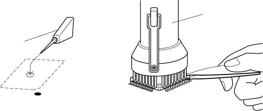
REPLACING THE DSP (HG51A115A01FD)
Note: To increase productivity ,the DSP HG51A115A01FD is sticked on the main PCB with a double-side
adhesive tape, then its leads are soldered.
Remove the DSP according to the following procedures.
1. Prepare isopropyl alcohol and a flat IC desoldering machine (Spot Heater HS-600).
2. Apply plenty of the alcohol to the adhesive tape from the reverse side of the main PCB. (Fig. 1)
There is a hole on the PCB just under the LSI, and the adhesive tape can be seen through the hole.
3. Leave it more than one minute so that the alcohol weaken adhesive power fully.
4. Using a proper size of nozzle, apply heat to leads of the LSI with the desoldering machine.
5. Grasp the LSI with tweezers, and using gentle force vibrate the tweezers to feel melting solder. (Fig.2)
6. Remove the LSI after meltingsolder at every leads wholly.
Alcohl
Spot Heater HS-600
Fig.2Fig.1
HG51A115A
LSI-S
— 3 —
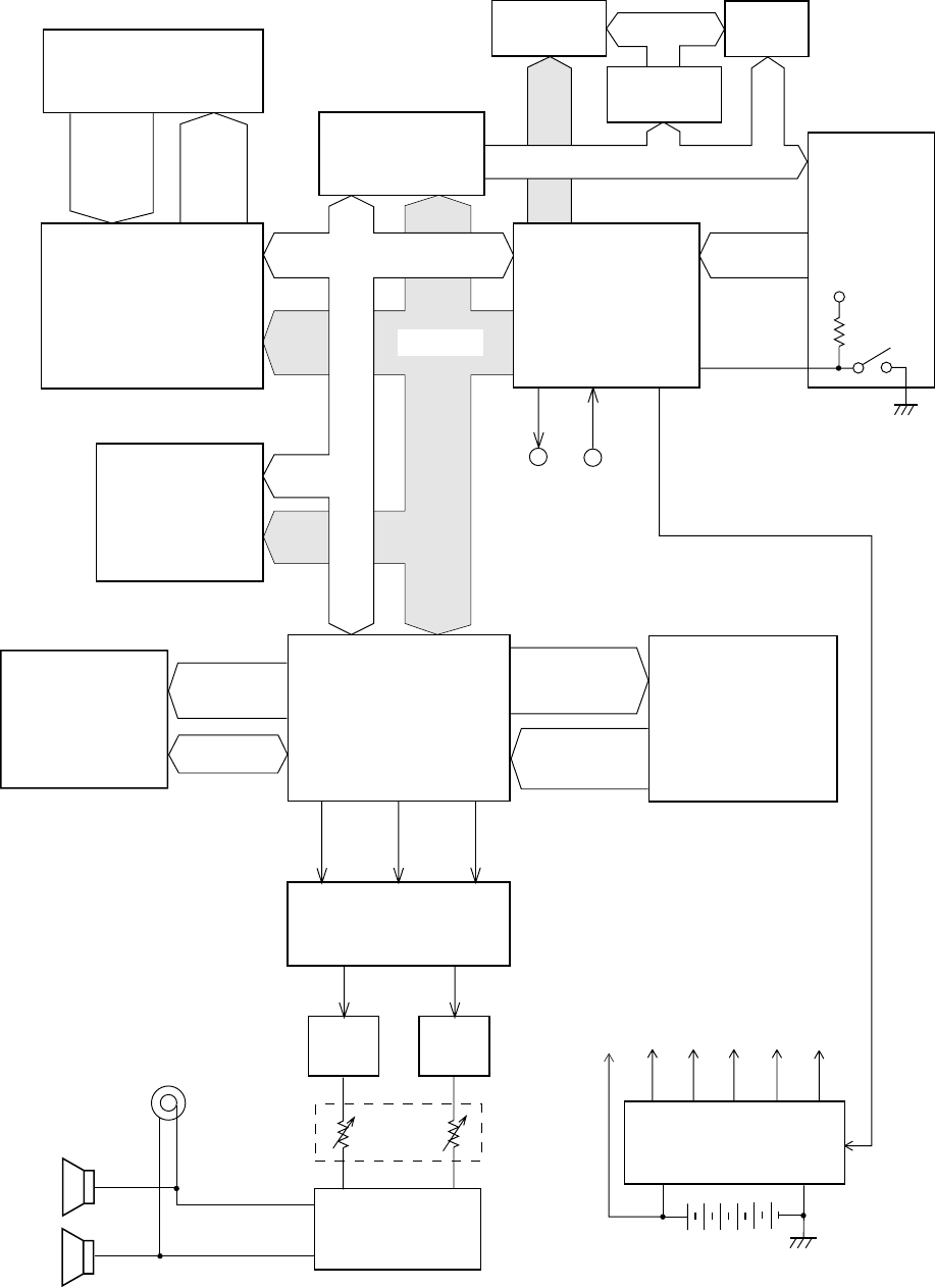
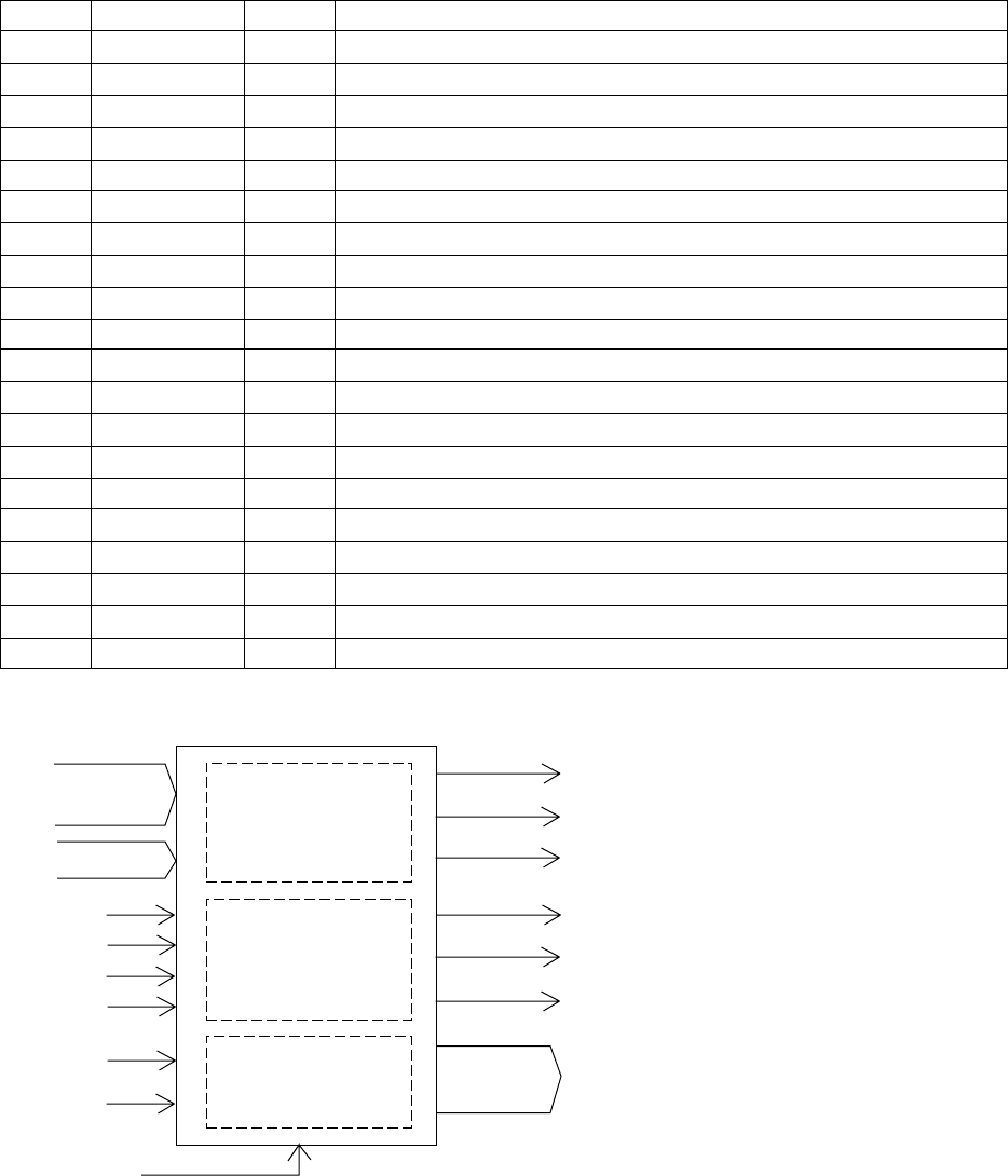
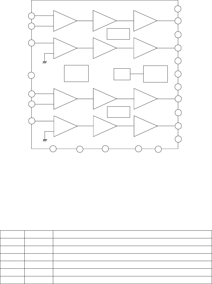
BLOCK DIAGRAM
KC0 ~
KC7
SI0 ~ SI7
FI0 ~ FI7
Key Touch LSI
HG52E35P
Working Strage
RAM (256K-bit)
HM62256ALP-10
Working Strage
RAM (256K-bit)
HM62256ALP-10
7-Segment
LED LO0 ~ LO4
LED driver
BA612
LD0 ~ LD7
KO0 ~ KO7
Buttons
KI1 ~ KI7
VDD
Power Switch
MIDI IN
OUT
EA0 ~ EA14
ED0 ~ ED7
DSP
HG51A115A01FD
RA0 ~ RA19
RD0 ~ RD15
Sound Source ROM
(16M-bit)
TC5316200CP-C081
WCK1 SLOP BCK
D/A Converter
UPD6376CX
Filter
Filter
Main
Volume
Power Amplifier
LA4620
Gate Array
UPD65005C-578
CPU
HD6433298A18P
Keyboard
A0 ~ A15 POWER
Power Supply Circuit
Q1 ~ Q7
VCC AVDD VDD
LVDD DVDD
VD
APO
Effect RAM
(256K-bit)
HM62256ALP-10
D0~D7
Speakers
Output
A0 ~ A14 A0 ~ A3
A0 ~ A2
LEDs
— 4 —
CIRCUIT DESCRIPTION
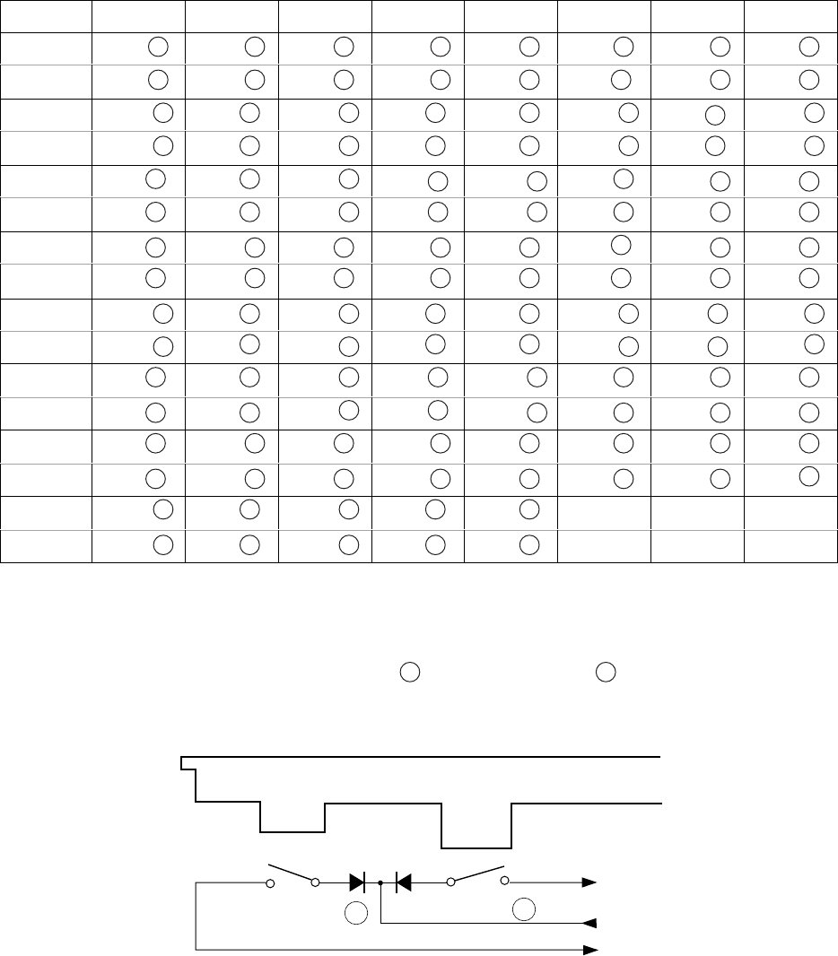
Key Matrix
Key
Second contact 2 First contact 1
FI
KC
SI
Note: Each key has two contacts, the first conatct 1 and second contact 2 .
KC0 KC1 KC2 KC3 KC4 KC5 KC6 KC7
FI0 C2 1 C#2 1 D2 1 D#2 1 E2 1 F2 1 F#2 1 G2 1
SI0 C2 2 C#2 2 D2 2 D#2 2 E2 2 F2 2 F#2 2 G2 2
FI1 G#2 1 A2 1 A#2 1 B2 1 C3 1 C#3 1 D3 1 D#3 1
SI1 G#2 2 A2 2 A#2 2 B2 2 C3 2 C#3 2 D3 2 D#3 2
FI2 E3 1 F3 1 F#3 1 G3 1 G#3 1 A3 1 A#3 1 B3 1
SI2 E3 2 F3 2 F#3 2 G3 2 G#3 2 A3 2 A#3 2 B3 2
FI3 C4 1 C#4 1 D4 1 D#4 1 E4 1 F4 1 F#4 1 G4 1
SI3 C4 2 C#4 2 D4 2 D#4 2 E4 2 F4 2 F#4 2 G4 2
FI4 G#4 1 A4 1 A#4 1 B4 1 C5 1 C#5 1 D5 1 D#5 1
SI4 G#4 2 A4 2 A#4 2 B4 2 C5 2 C#5 2 D5 2 D#5 2
FI5 E5 1 F5 1 F#5 1 G5 1 G#5 1 A5 1 A#5 1 B5 1
SI5 E5 2 F5 2 F#5 2 G5 2 G#5 2 A5 2 A#5 2 B5 2
FI6 C6 1 C#6 1 D6 1 D#6 1 E6 1 F6 1 F#6 1 G6 1
SI6 C6 2 C#6 2 D6 2 D#6 2 E6 2 F6 2 F#6 2 G6 2
FI7 G#6 1 A6 1 A#6 1 B6 1 C7 1
SI7 G#6 2 A6 2 A#6 2 B6 2 C7 2
— 5 —
Nomenclature of Keys
F#3 G#3 A#3 C#4 D#4 F#4 G#4 A#4 C#5 D#5 F#5 G#5 A#5
F3 G3 A3 B3 C4 D4 E4 F4 G4 A4 B4 C5 D5 E5 F5 G5 A5 B5 C6
D#3
C2 D2 E2 F2 G2 A2 B2 C3 D3 E3 B6A6G6F6E6D6 C7
C#3A#2G#2
F#2D#2
C#2 A#6
G#6F#6D#6
C#6
Button Matrix
KI1 KI2 KI3 KI4 KI5 KI6 KI7
KO0 Split Layer Upper 1 Lower 1 Lower 2 Upper 2
KO1 Transpose Tune MIDI Jack Rhythm Tone Play Style
KO2 Track 4
Chord 1 Track 5
Chord 2 Track 6
Chord 3 Track 2
Rhythm Track 3
Bass
KO3 3 6 9 Demo Touch
Responce Digital
Effect Resistration
KO4 2 5 8 Track 1 1 4 7
KO5 Accomp.
Volume Song
Memory Accomp. Track 0 - +
KO6 Synchro/
Ending Variation
/Fill-In Normal/
Fill-In Intro F D B
KO7 Mode A C E Start/
Stop Tempo
Down Tempo
Up
Reset Circuit
VDD Battery set
RESET
CPU
HD6433298A18P
Reset IC
S8053ANO
Working Strage RAM
HM62256ALP-10
Gate Array
UPD65005C-578
DSP
HG51A115A01FD
Key Touch LSI
HG52E35
DVDD
DVDD
VDD
VDD
VDD
-RESET
WR -SRAM
POWER
From power switch

— 6 —
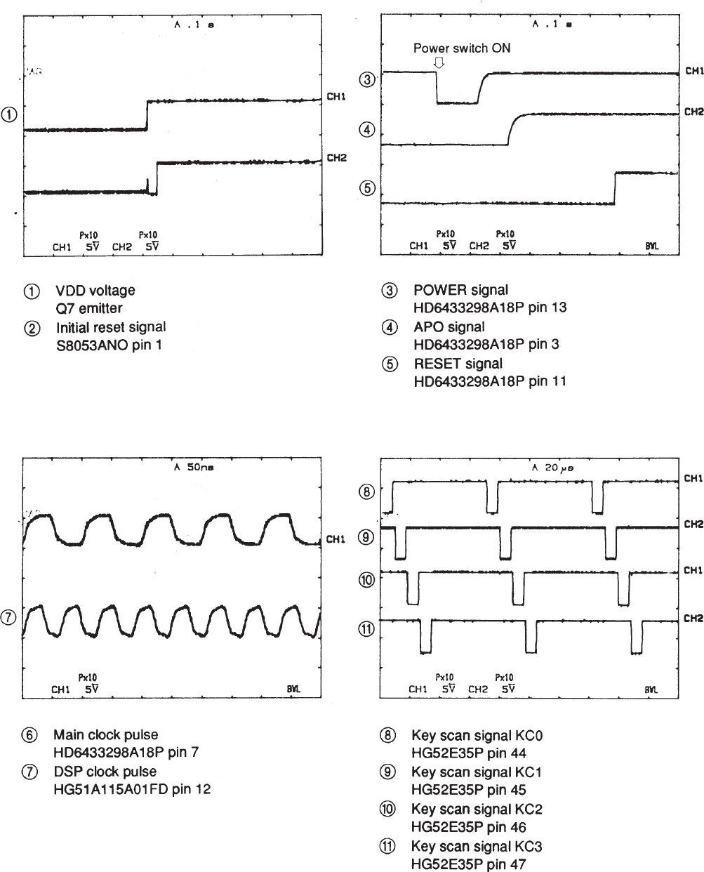
Pin No. Terminal In/Out Function
1 P40 Out KO signal data output
2 P41 Out Clock for KO signal data
3 P42 Out APO (Auto Power Off) signal output. ON: High, OFF: Low
4 P43 Out Read enable signal output
5 P44 Out Write enable signal output
6 P45 Not used.
7 P46 Out 10MHz clock output
8 P47 In Wait signal input. Connected to +5V.
9 TXD Out MIDI signal output
10 RXD In MIDI signal input
11 P52 Out Reset signal output
12 -RESET In Reset signal input
13 -NMI In Power ON signal input.
14 VCC In +5V source
15 -STBY In Standby signal input. Connected to +5V.
16 VSS In Ground (0V) source
17 XTAL In 20MHz clock input
18 EXTAL In 20MHz clock input
19, 20 MD1, MD0 In Mode selection input. (Internal ROM mode --- MD1: Hight, MD0: Low)
21 AVSS In Ground (0V) source for internal DAC
22 AN0 In Analog input. Connected to the bender volume.
23 ~ 29 P71 ~ P77 In Button input signal input
30 AVCC In +5V source for internal DAC
31 ~ 38 P60 ~ P67 Out LED segment signal output
39 VCC In +5V source
40 ~ 56 P27 ~ P10 Out Address bus
48 VSS In Ground (0V) source
57 ~ 64 P30 ~ P37 Ijn/Out Data bus
Initial reset
When batteries are set or an AC adapter is connected, the reset IC provides a low pulse to the CPU.
The CPU then initializes its internal circuit and clears data in the working strage RAM.
Power ON reset
When the power switch is pressed, the CPU receives a low pulse of POWER signal. The CPU first raises
APO signal to +5V to generat DVDD voltage, then raises RESET signal to +5V. During this period the
gate array, the DSP and the key touch LSI initializes their internal circuit.
CPU (HD6433298A18P)
The 16-bit CPU contains a 32k-bit ROM, a 1k-bit RAM, seven 8-bit I/O ports, an A/D convertor and serial
interfaces. The CPU accesses to the working strage RAM, the DSP and the key touch LSI. The CPU also
controls buttons, LEDs, bender input and MIDI input/output.
— 7 —
Gate Array (UPD65005C-578)
Functions of the gate array are;
(1) To decode chip select signals for the working strage RAM, the DSP and the key touch LSI.
(2) To hold the following signals on "Low" during power off.
Read/write enable signals for the DSP and the key touch LSI
10MHz clock for the key touch LSI
(3) To generate button scan / LED drive signals.
The following table shows the pin functions of the gate array.
A4 ~ A15
D0, D1
RD
WR
PHA
APO
KOD
KOC
RESET
LSIS
HG
SRAM
RDAPO
WRAPO
PHAPO
KO0 ~ KO7
Address decoder
Controller
Shift register
(Chip select sigal for the DSP)
(Chip select signal for the key touch LSI)
(Chip select signal for the working strage RAM)
(Read enable signal controlled by APO)
(Write enable signal controlled by APO)
(10MHz clock for the key touchLSI.
Controlled by APO)
(Button scan / LED drive signal)
Pin No. Terminal In/Out Function
1 -RESET In Reset signal input
2 -RDAPO Out Read enable signal output
3 -WRAPO Out Write enable signal output
4 -LSIS Out Chip select signal for the DSP
5 -HG Out Chip select signal for the key touch LSI
6 PHAPO Out 10MHz clock for the key touch LSI
7 -SRAM Out Chip select signal for the working strage RAM
8 ~ 9 KO8 ~ KO9 Not used.
10 ~ 17 KO7 ~ KO0 Out Button scan / LED drive signal output
18 ~ 20 Not used.
21 GND In Ground (0V) source
22 PHA In 10MHz clock input
23 -WR In Write enable signal input
24 -RD In Read enable signal input
25 -APO In APO (Auto Power Off) signal input
26 KOC In KO signal data input
27 KOD In Clock for KO signal data
28 ~ 39 A15 ~ A4 In Address bus
40, 41 D0, D1 In Data bus
42 VDD In +5V source

— 8 —
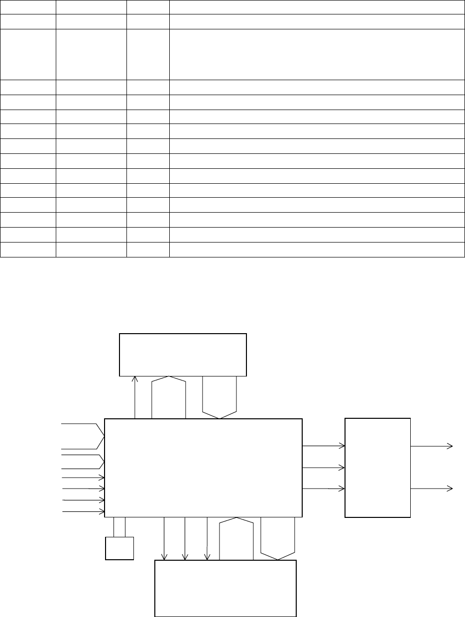
Digital Signal Processor (HG51A115A01FD)
Upon receipt of note numbers and their velocities, the DSP reads sound and velocity data from the sound
source ROM in accordance with the selected tone; the DSP can read rhythm data simultaneously when a
rythm pattern is selected. Then it provides 16-bit serial signals containing data of the melody, chord, bass,
and percussion to the DAC. The DSP also adds the selected effect to the sound data using a 256k-bit
RAM.
The following table shows the pin functions of the DSP.
Pin No. Terminal In/Out Function
1 ~ 8 CD0 ~ CD7 In/Out Data bus
9, 10 Not used.
11 GND7 In Ground (0V) source
12 CK16 Out 16.384MHz clock output
13 VCC6 In +5V source
14 CK0 In Clock input. Connected to terminal CK16.
15 TCKB Not used.
16 VCC1 In +5V source
17 GND1 In Ground (0V) source
18, 19 XT0, XT1 In/Out 16.384MHz clock input/output. Connected to a crystal oscillator.
20 SGL In System control terminal. Single chip system: Open
21 CCSB In Chip select signal input
22 ~ 25 CA0 ~ CA3 In Addess bus
26 CE0 In Not used. Connected to ground.
27 CWRB In Write enable signal
28 CRDB In Read enable signal
29 ~ 32 Not used.
33 RESB In Reset signal input
34 TESB In Not used. Connected to +5V.
35 ~ 39 Not used.
40 ~ 49
52 ~ 57 RD0 ~ RD15 In Data bus for the sound source ROM
58 RA23 Out Not used.
59 RA22 Out Chip select signal for the sound source ROM
60, 61 RA20, RA21 Out Not used.
62 ~ 73
75 ~ 82 RA0 ~ RA19 Out Data bus for the sound source ROM
74 GND5 In Ground (0V) source
83 WOK2 Out Word clock output. Not used.
84 VCC3 In +5V source
85 GND3 In Ground (0V) source
86 WOK1 Out Word clock for the DAC
87 SOLM Out Serial data output. Not used.
88 SOLP Out Serial data output for the DAC
89 BOK Out Bit clock output for the DAC
90 ~ 92 Not used.
— 9 —
DSP
HG51A115A01FD
Effect RAM (256K-bit)
HM65256BLP
Sound Source ROM
TC5316200CP-C081
CE A0 ~ A19 D0 ~ D15
RA0 ~
RA19
RD0 ~
RD15
RA22
D0 ~ D7
A0 ~ A3
LSIS
RDAPO
WRAPO
RESET
SOLP
BOK
WOK1
EA0 ~
EA14
ED0 ~
ED15
CS WE
OE
D0 ~ D15 A0 ~ A14
ECEB EOEB EWEB
PG
16.384MHz
DAC
UPD6376CX
LOUT
ROUT
SOLP: Sound data
BOK: Bit clock
WOK1: Word clock
SI
CLK
LRCK
Block diagram of DSP and DAC circuit
Pin No. Terminal In/Out Function
93 VCC5 In +5V source
94, 95
97 ~ 105
107,109
110, 112
EA0 ~ EA14 Out Address bus for the effect RAM
96 EWEB Out Write enable signal output for the effect RAM
106 EOEB Out Read enable signal output for the effect RAM
108 VCC7 In +5V source
111 ECEB Out Chip select signal output for the effect RAM
113 ~ 117 Not used.
118 VCC4 In +5V source
119 GND4 In Ground (0V) source
120 ~ 122 Not sued.
123 ~ 130 ED0 ~ ED7 In/Out Data bus for the effect RAM
131 GND5 In Ground (0V) source
132 ~ 134 Not used. Connected to ground.
135, 136 Not used.
— 10 —
DAC (UPD6376CX)
UPD6376CX is a two-channel 16-bit Digital to Analog Convertor consisting of resistor string, output
amplifier and zero offset circuit.
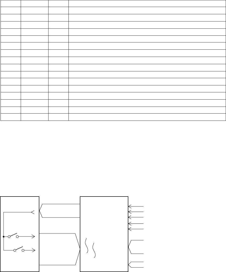
Key Touch LSI (HG52E35P)
By counting the time between first-key input signal FI and second-key SI from the keyboard unit, the key
touch LSI detects key velocity of 256-step. Then the LSI sends the CPU the note number and its velocity
data.
RESB
CCSB
CWRB
CRDB
CKI
CD0
CD7
CA0 ~ CA2
First contact
Second contact
KC0
KC7
FI0
FI7
SI0
SI7
Key input signal
Key scan signal
~
Data bus
Address bus
Reset signal from the CPU
Chip select signal from the gate array
Read enable signal from the gate array
Write enable signal from the gate array
Clock from the gate array
Key touch LSI
HG52E35P
Keyboard
FI
SI
KC
Pin No. Terminal In/Out Function
1 SEL In Mode selection terminal. Connected to ground.
2 D.GND In Ground (0V) source for internal digital circuit
3 NC Not used.
4 DVDD In +5V source for internal digital circuit
5 A.GND In Ground (0V) source for internal analog circuit
6 R.OUT Out Sound waveform output
7 A.VDD In +5V source for internal analog circuit
8 A.VDD In +5V source for internal analog circuit
9 R.REF In Reference voltage terminal. Connected to a capacitor.
10 L.REF In Reference voltage terminal. Connected to a capacitor.
11 L.OUT Out Left channel sound waveform output
12 A.GND In Ground (0V) source for internal analog circuit
13 LRCK In Word clock (L/R separation signal) input.
14 LRSEL In Not used. Connected to ground.
15 SI In Sound data input
16 CLK In Bit clock input
— 11 —
The following table shows the pin functions of the key touch LSI.
Pin No. Terminal In/Out Function
1 REQB Out Interrupt request. Not used.
2, 3 FI10, SI10 In Key input signal
4 VCC In +5V source
5 CRDB In Read enable signal
6 CWRB In Write enable signal
7 CCBB In Chip select signal
8, 9 T, STBY In Not used. Connected to +5V.
10 RESB In Reset signal
11 W In Not used. Connected to +5V.
12 CKI In 10 MHz clock input
13, 14 TMD, TST In Not used. Connected to ground.
15 CKO Out Not used.
16 GND In Ground (0V) source
17 XIN In Not used. Connected to ground.
18 XOUT Out Not used.
19 TRES In Not used. Connected to ground.
20 ~ 23, 25 ~ 28 CD0 ~ CD7 In/Out Data bus
24 GND In Ground (0V) source
29 ~ 31 CR0 ~ CR2 In Address bus
32 VCC In +5V source
33 ~ 39, 41 ~ 43
53 ~ 55, 57 ~ 63 FI0 ~ FI9,
SI0 ~ SI9 In Key input signal
40 VCC In +5V source
44 ~ 47, 49 ~ 52 KC0 ~ KC7 Out Key scan signal
48, 56 GND In Ground (0V) source
64 VCC In +5V source
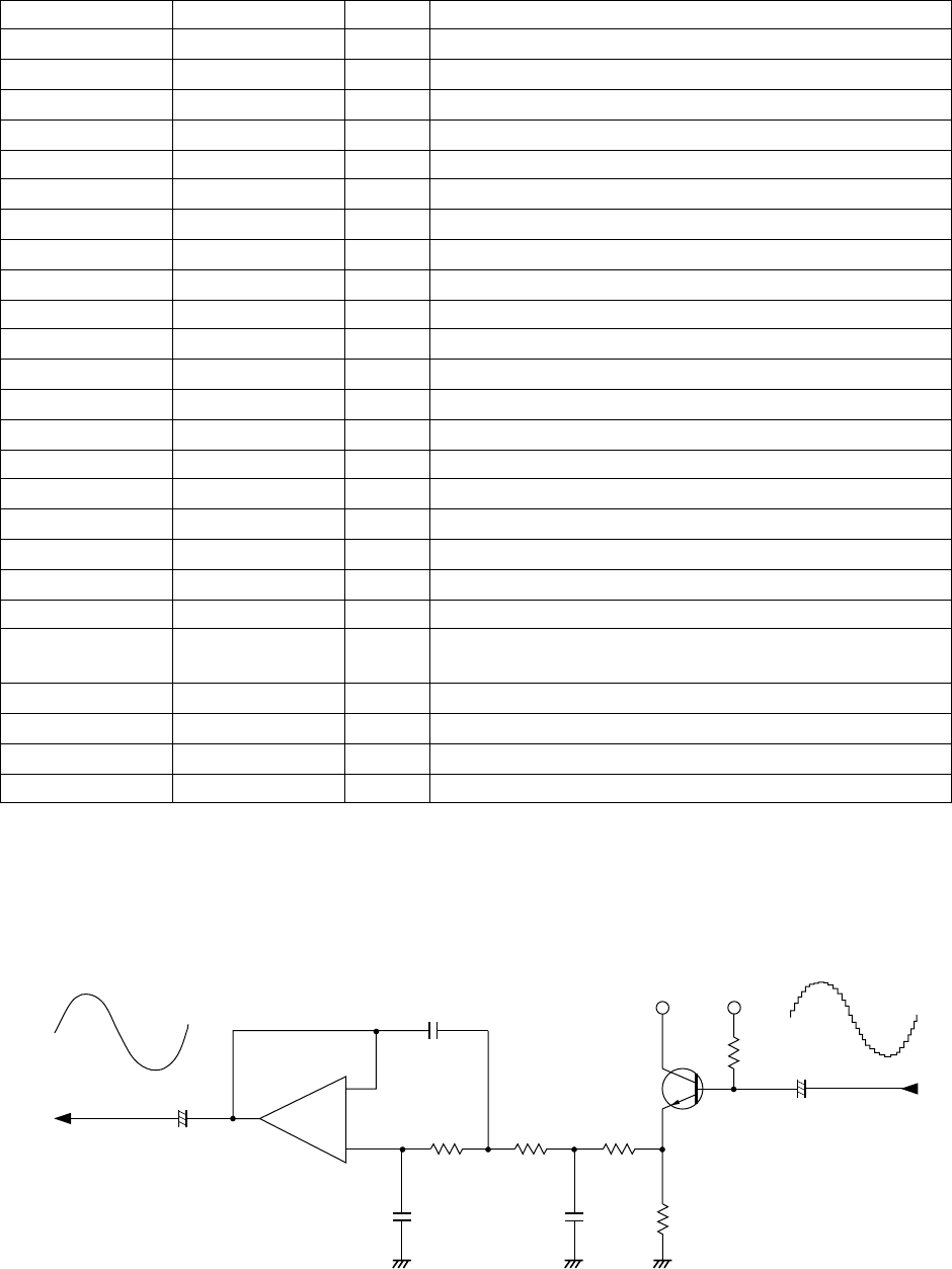
Filter Block
Since the sound signals from the DAC are stepped waveforms, the filter block is added to smooth the
waveforms.
AVDD
1K 1K 1K
C182(H)
C152(H)
AG AG
1K
AG
To main volume
-
+
M5218APR
10V22µ
C104(H)
2SC1740SQ
10K
AVEE
10V22µ
From the DAC
— 12 —
Power Amplifier (LA4620)
The power amplifier is a two-channel balanced amplifier with standby switch. The following figure shows
the internal diagram of the amplifier.
Internal Diagram of LA4620
Input
Amp. Pre-drive
Amp.
Power
Amp.
RL Short
Protector
Input
Amp. Pre-drive
Amp.
Power
Amp.
Terminal
Protection
Circuit
Ripple
Filter
Pop Noise
Prevention
Circuit
Input
Amp. Pre-drive
Amp.
Power
Amp.
RL Short
Protector
Input
Amp. Pre-drive
Amp.
Power
Amp.
16 10 11 13
2
12
14
15
17
18
1
23
22
21
20
19
3
5
4
9
7
8
6
IN11+
IN11-
IN12-
PriGND
IN21+
IN21-
IN22-
NC DC MUTE VCC2 ADJ
Boot22
OUT22
PoGND2
OUT21
Boot21
VCC1
Boot21
OUT12
PoGND1
OUT11
Boot11
+
-
-
+
+
-
-
+
Power Supply Circuit
The power supply circuit generates six voltages as shown in the following table. VDD voltage is always
generated. The others are controlled by APO signal from the CPU.
Name Voltage For operation of
VDD +5.1V CPU, Reset IC, Gate array, Working strage RAM
DVDD +5.3V DSP, Key touch LSI, Sound source ROM, Effect RAM, DAC
AVDD +5.2V DAC, Filter
LVDD +5.2V LED driver
VCC +12V Pilot lamp
VD +12V Power amplifier
— 13 —
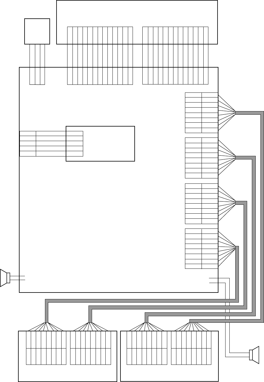
WIRING DIAGRAM
FI1
FI2
FI0
SI0
SI1
SI2
SI3
FI3
KC0
KC1
KC2
KC3
KC4
KC5
KC6
KC7
KC0
KC1
KC2
KC3
KC4
KC5
FI4
SI4
KC6
KC7
SI5
SI6
SI7
FI5
FI6
FI7
LG
PWLD
KO7
KO6
KO5
KO4
KO3
KO2
KO1
KO0
POWER
KI1
KI2
KI3
KI4
KI5
KI6
KI7
La
Lb
Lc
Ld
Le
Lf
Lg
Lp
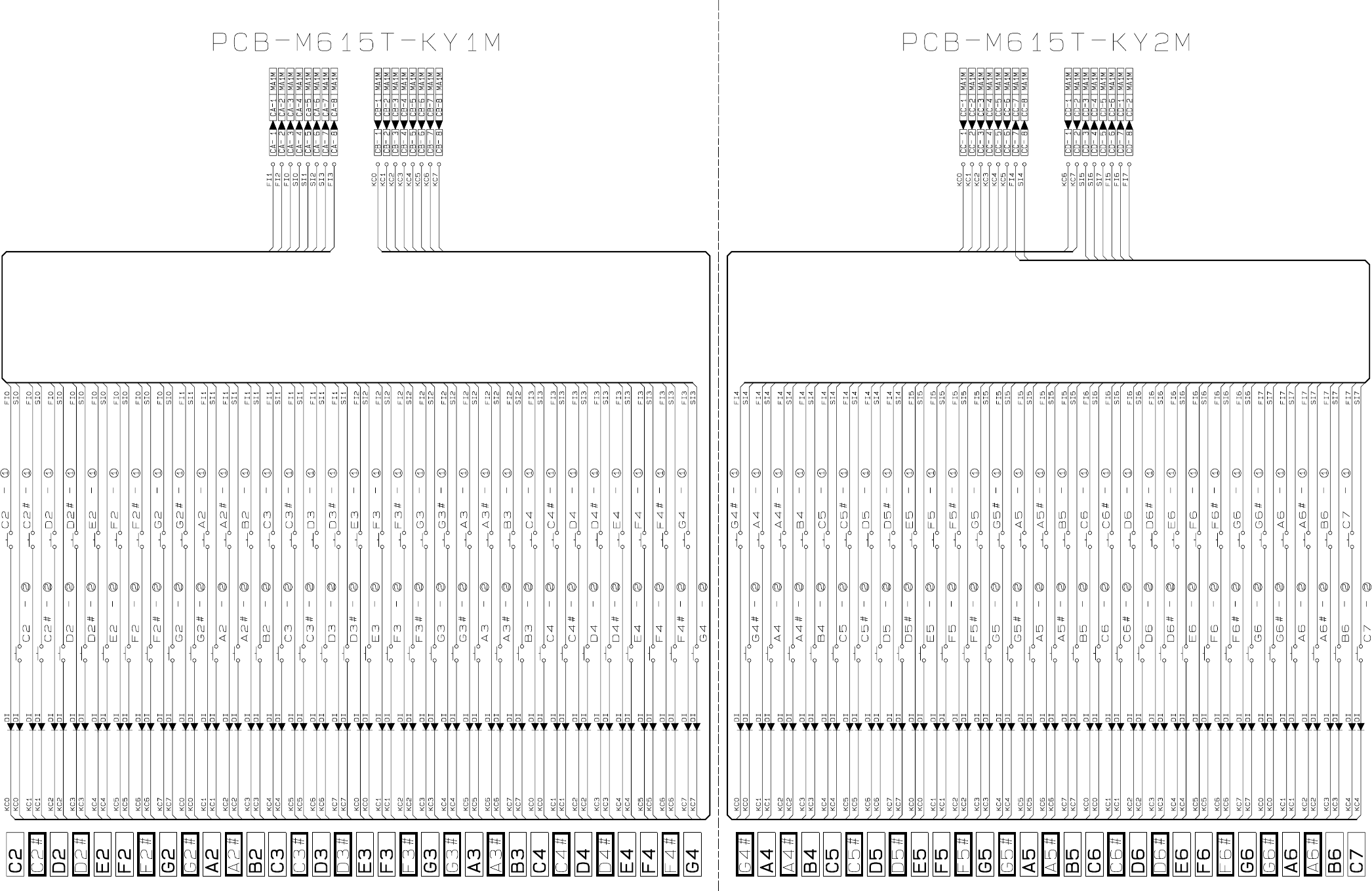
M615T-KY2M
M615T-KY1M
CD1
CD2
CD3
CD4
CD5
CD6
CD7
CD8
CC1
CC2
CC3
CC4
CC5
CC6
CC7
CC8
CB1
CB2
CB3
CB4
CB5
CB6
CB7
CB8
CA1
CA2
CA3
CA4
CA5
CA6
CA7
CA8
CA8
CA7
CA6
CA5
CA4
CA3
CA2
CA1
FI3
SI3
SI2
SI1
SI0
FI0
FI2
FI1
CB8
CB7
CB6
CB5
CB4
CB3
CB2
CB1
KC7
KC6
KC5
KC4
KC3
KC2
KC1
KC0
CC8
CC7
CC6
CC5
CC4
CC3
CC2
CC1
SI4
FI4
KC5
KC4
KC3
KC2
KC1
KC0
CD8
CD7
CD6
CD5
CD4
CD3
CD2
CD1
FI7
FI6
FI5
SI7
SI6
SI5
KC7
KC6
JG1
JG2
JG3
JG4
JG5
JG6
JG7
JG8
JG9
JG10
JG11
JG12
JG13
JH1
JH2
JH3
JH4
JH5
JH6
JH7
JH8
JH9
JH10
JH11
JH12
JH13
JG1
JG2
JG3
JG4
JG5
JG6
JG7
JG8
JG9
JG10
JG11
JG12
JG13
JH1
JH2
JH3
JH4
JH5
JH6
JH7
JH8
JH9
JH10
JH11
JH12
JH13
JE5
JE4
JE3
JE2
JE1
AG
LMELO OUT
RMELO OUT
RMELO IN
LMELO IN
JE5
JE4
JE3
JE2
JE1
W
BL
PR
PR
PS
W
O
BK
R
JF3
JF2
JF1
DVDD
BENDER
DG
Bender
Volume
M5712-CN1M
M5172-MA2M
Main Volume
A5712-MA1M
Green
Yellow
Red Blue
— 14 —
MAJOR WAVEFORMS
— 15 —
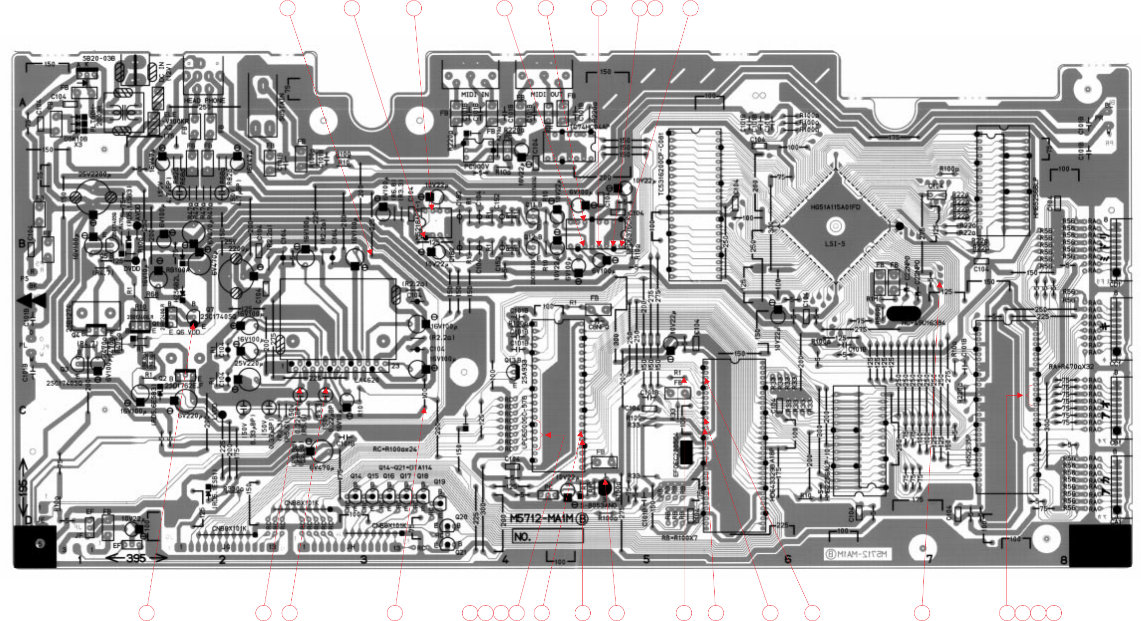
— 16 —
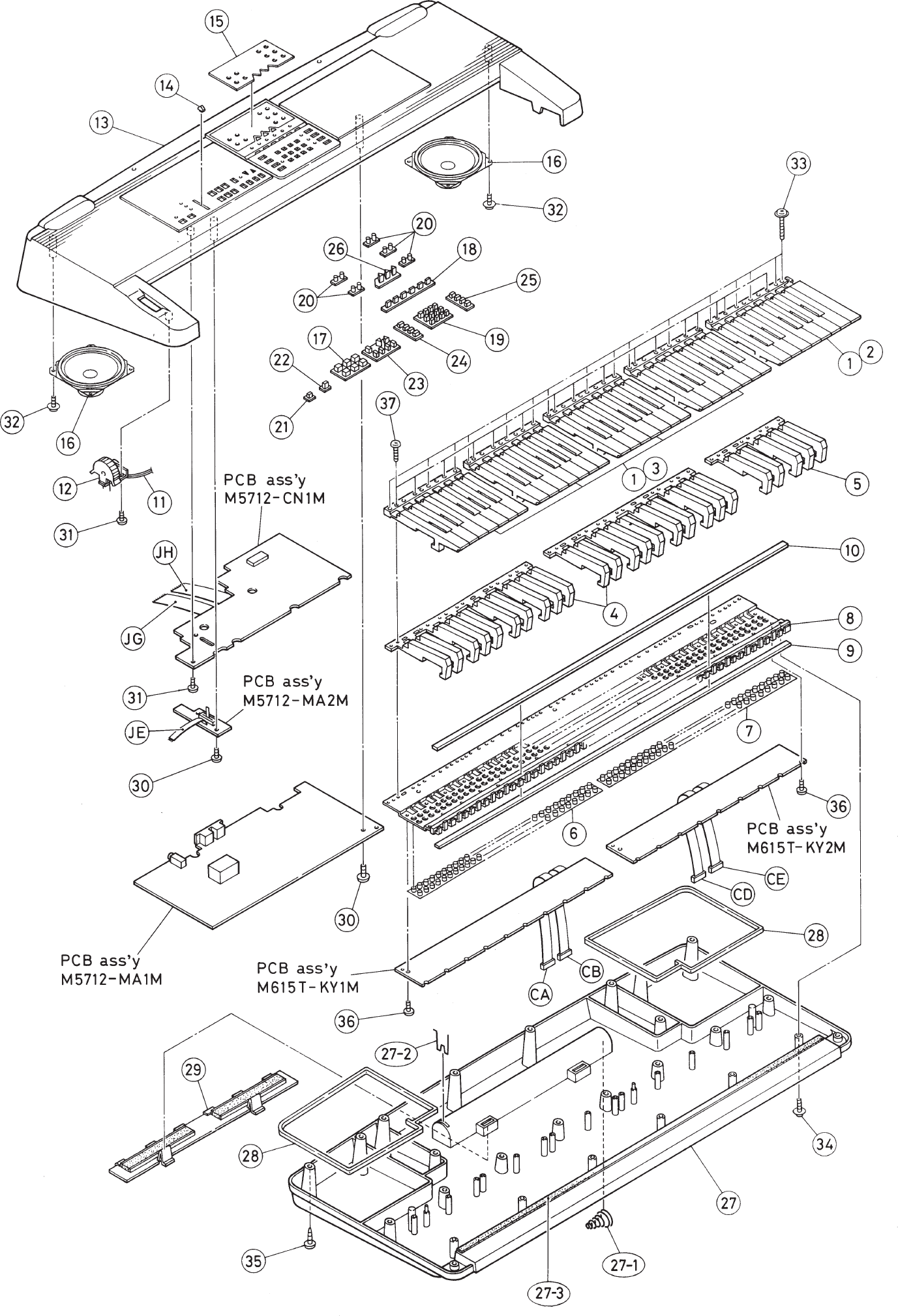
1
21
9 10 1127 26 29 14 15 16 17 13 12 2 6 3 5 4 7 8
28 24 25 1922 23 20 18
PCB VIEW and MAJOR CHECK POINTS
— 17 —
11.6
11.6
11.4
10.9
10.9
5.2
0.0
0.0
0.0
0.7
5.3
5.3
2.6 2.6
2.6
2.6
2.6 2.6
2.6
2.6
5.9
11.6
11.8 5.1
5.8 5.2
5.3
0.7
0.0
5.2
5.2
3.2
3.2
3.4
11.0 1
2
3
4
5
6
12
13
18
25
26
27
28
29
24 22
23
19
7
8 9 10 11
14 15
16 17
21
20
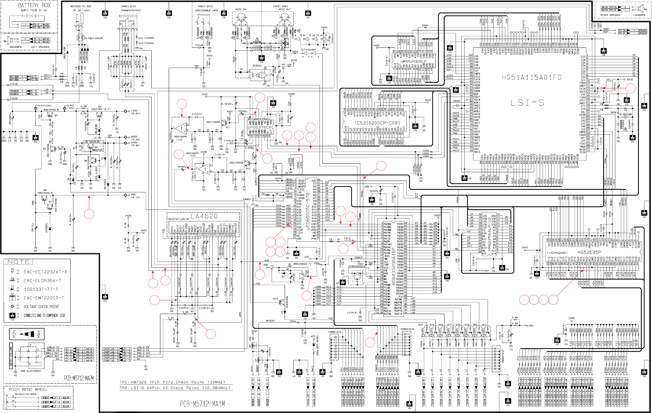
SCHEMATIC DIAGRAMS
Main PCB M5712-MA1M
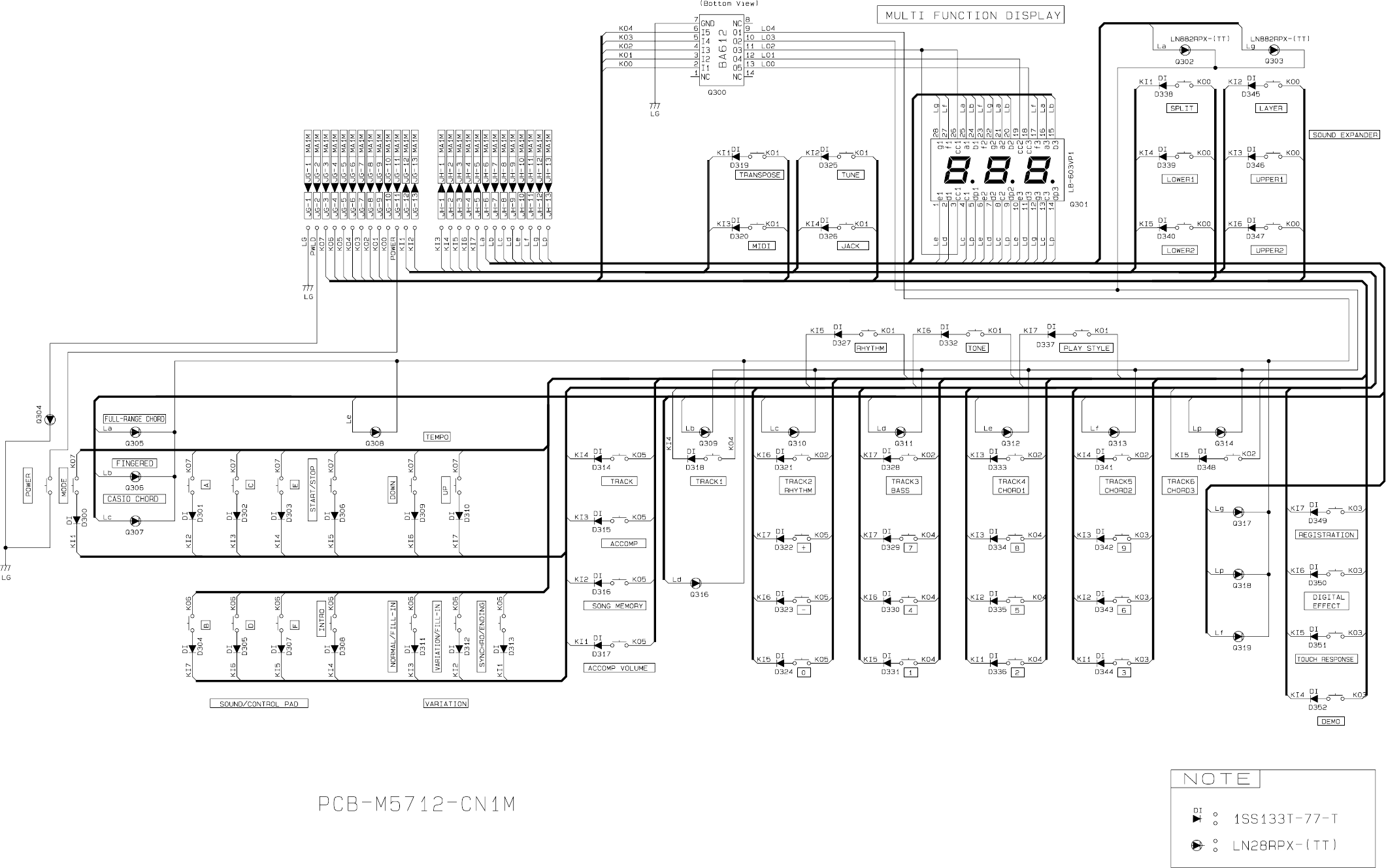
— 18 —
Console PCB M5712-CN1M
— 19 —
Keyboard PCBs M615T-KY1M, KY2M
— 20 —
EXPLODED VIEW
— 21 —
IC LEAD IDENTIFICATION AND INTERNAL DIAGRAM
TIMING
GENERATOR
SHIFT REGISTER
LATCH
MAIN DAC
SUB DAC
SUB DAC
MAIN DAC
LRCK
LRSEL/RSI
SI/LSI
CLK
4/8 fs SEL
D.GND
N.C. D.VDD A.GND A.VDD
R.OUT
R.REF
L.REF
L.OUT
11
10
9
6
8
712
54
3
13
14
15
16
1
2
3
2
1OUT
VDD
VSS
123
45
6
VCC GND
NC
+
-
+
-
1234
5
67
8
VCC
GND
1A 1
1Y 2
2A 3
2Y 4
3A 5
3Y 6
GND 78
9
10
11
5Y
12
6A13
6Y
14 VCC
4A
4Y
5A
UPD6376CX
TC74HC04AP M5218APR PC900V
S8053ANO
1 2 3
— 22 —
B C E B C E
E C B E C B
Q2: 2SD1762E,F Q4: 2SB1274
Q3, Q5, Q7, Q11/12: 2SC1740SQ
Q13: 2SA933SQ
Q14~21: DTA114TS
Q1/6: 2SB1240Q,R

PARTS LIST
CTK-750
Notes: 1. Prices and specifications are subject to change with-
out prior notice.
2. As for spare parts order and supply, refer to the
"GUIDEBOOK for Spare parts Supply", published
separately.
3. The numbers in item column correspond to the same
numbers in drawing.
FOB Japan
N Item Code No. Parts Name Specification Q M N.R.Yen R *
Unit Price
PCB Ass'y M5712-MA1M
2010 4928 LSI HM65256BLP-10 1 1 720 A H
2011 3325 LSI UPD6376CX 1 1 230 A C
2011 5194 LSI HG52E35P 1 1 600 A F
2011 5201 LSI HG51A115A01FD 1 1 2,820 A T
N 2011 5810 LSI UPD43256AC-85L,10L 1 1 620 A F
N 2011 6867 LSI UPD65005C-578 1 1 220 A C
N 2011 7196 LSI TC5316200CP-C081 1 1 1,230 A N
N 2011 7203 LSI HD6433298A18P 1 1 880 A J
2105 2219 IC S-8053ANO 1 1 60 A B
N 2105 3164 IC HD74HC04P 1 1 28 A A
2114 1421 Photo-coupler PC900V 1 1 210 A C
2114 1799 IC M5218APR 1 1 38 A A
2114 1883 IC LA4620 1 1 350 A D
2250 0441 Transistor 2SA1267Y-AT-T 1 10 9 A A
2251 0140 Transistor 2SB1240Q,R-TV6-T 2 10 10 A A
2251 0672 Transistor 2SB1548-P.CS 1 10 44 A A
2252 0497 Transistor 2SC3199Y-AT-T 5 10 9 A A
2253 0455 Transistor 2SD1762E,F 1 1 47 A A
2259 1883 Digital transistor DTA114TS-TP-T 8 10 10 A A
2360 1729 Zener diode MTZJ5.1AT-77-T 1 10 8 B A
2360 1946 Zener diode MTZJ5.6CT-77-T 1 10 8 B A
N 2360 2254 Zener diode HZS6B2LTD-T 1 10 9 B A
N 2360 2261 Zener diode RD5.1JSB3-T1-T 1 10 9 B A
2390 0371 Diode DSK10B-BT-T 3 10 11 C A
2390 1323 Diode RB100A-T32-T 1 10 29 C A
2390 1344 Diode 1SS133T-77-T 5 20 3 C A
2390 1463 Schottky diode SB20-03B 1 5 39 C A
2590 1519 Crystal oscillator HC-49U16384 1 1 100 B B
N 2590 1547 Ceramic oscillator EFO-EC2005C4 1 5 64 B B
2606 1141 Carbon film resistor R-20-1K-J-T23-T 16 20 2 C A
2606 1148 Carbon film resistor R-20-220-J-T23-T 4 20 2 C A
2606 1155 Carbon film resistor R-20-330-J-T23-T 1 20 2 C A
2606 1162 Carbon film resistor R-20-10-J-T23-T 5 20 2 C A
2606 1169 Carbon film resistor R-20-100-J-T23-T 33 20 2 C A
2606 1176 Carbon film resistor R-20-100K-J-T23-T 9 20 2 C A
2606 1183 Carbon film resistor R-20-10K-J-T23-T 7 20 2 C A
2606 1197 Carbon film resistor R-20-22-J-T23-T 8 20 2 C A
2606 1232 Carbon film resistor R-20-82-J-T23-T 2 20 2 C A
2606 1253 Carbon film resistor R-20-4.7K-J-T23-T 2 20 2 C A
2606 1302 Carbon film resistor R-20-270-J-T23-T 1 20 2 C A
2606 1309 Carbon film resistor R-20-470-J-T23-T 36 20 2 C A
2606 1323 Carbon film resistor R-20-56K-J-T23-T 22 20 2 C A
2606 1330 Carbon film resistor R-20-68K-J-T23-T 1 20 2 C A
2606 1337 Carbon film resistor R-20-1M-J-T23-T 1 20 2 C A
2606 1358 Carbon film resistor R-20-3.3K-J-T23-T 3 20 2 C A
2606 1372 Carbon film resistor R-20-33K-J-T23-T 11 20 2 C A
2606 1428 Carbon film resistor R-20-5.6K-J-T23-T 2 20 2 C A
2606 1435 Carbon film resistor R-20-560-J-T23-T 1 20 2 C A
2606 1491 Carbon film resistor R-20-6.8K-J-T23-T 1 20 2 C A
2606 1694 Carbon film resistor R-20-68-J-T23-T 2 20 2 C A
2606 1708 Carbon film resistor R-20-47-J-T23-T 4 20 2 C A
N 2606 1722 Carbon film resistor R-20-2.2-J-T23-T 4 20 2 C A
N 2606 1757 Carbon film resistor R-20-6.8-J-T23-T 4 20 2 C A
2800 9091 Electrolytic capacitor 25RE2-220-T2-T 1 10 33 C A
Notes: N – New parts
M – Minimum order/supply quantity
R – Rank — 23 —
FOB Japan
N Item Code No. Parts Name Specification Q M N.R.Yen R *
Unit Price
2802 9231 Electrolytic capacitor 25RE3-2200-S1 2 10 75 C A
N 2803 6743 Electrolytic capacitor 50RBP2-R22-T2-T 2 20 16 C A
N 2803 6750 Electrolytic capacitor 50RBP2-R33-T2-T 2 20 16 C A
N 2803 6757 Electrolytic capacitor 50RBP2-4R7-T2-T 2 20 18 C A
2805 3061 Electrolytic capacitor 6.3RE2-220-T2-T 1 10 26 C A
2805 3134 Electrolytic capacitor 10RE2-22-T2-T 10 20 14 C A
2805 3142 Electrolytic capacitor 16RE2-10-T2-T 2 20 14 C A
2807 1015 Electrolytic capacitor 16RE2-47-T2-T 2 10 20 C A
2807 1040 Electrolytic capacitor 6.3RE2-470-T2-T 3 10 27 C A
2807 1082 Electrolytic capacitor 16RE2-100-T2-T 8 10 27 C A
2807 1091 Electrolytic capacitor 6.3RE2-100-T2-T 6 20 18 C A
2813 1722 Semiconductive capacitor DD407SR104K16-T 2 20 9 C A
2813 2597 Ceramic capacitor RT-HE40TKCH080D-T 1 20 5 C A
2813 3283 Ceramic capacitor UP050F104Z-A-B 22 20 8 C A
N 2813 3381 Semiconductive capacitor DD404SR152K16-T 2 20 5 C A
N 2813 3388 Semiconductive capacitor DD404SR182K16-T 2 20 5 C A
2818 0446 Ceramic capacitor RT-HE40TKYB101K-T 22 20 4 C A
2818 3275 Ceramic capacitor RT-HE40TKCH220J-T 2 20 5 C A
2830 6229 Mylar capacitor AMZV-104K50-T 6 10 13 C A
2845 0168 Module capacitor CNB8X101K 3 5 58 C B
2845 3213 Three-polarity capacitor EXC-ECT223ZVT-T 2 10 14 C A
2845 3220 Ferrite beads EXC-ELDR35V-T 20 10 12 C A
3025 0826 EMI filter EXC-EMT222DT-T 3 10 21 C A
3501 4816 DIN jack YKF51-5051 1 1 110 C A
3501 5012 DC jack HEC2305-01-920 1 10 25 A A
3501 7651 Connector S8B-PH-K-E 1 10 25 C A
3501 7658 Connector S8B-PH-K-M 1 10 25 C A
3501 7665 Connector S8B-PH-K-R 1 10 25 C A
3501 7672 Connector S8B-PH-K-Y 1 10 25 C A
3612 0711 Miniature jack YKB21-5101 1 5 90 B A
3612 0789 Jack YKB21-5010 1 5 60 B B
3719 2695 Heat sink OSH2742-L25-SP 1 1 150 C B
3719 4032 Heat sink UOT-10CS25-SPL 1 5 65 C B
3841 0539 Inductor ELE-V100KR-T 2 20 26 C A
3841 0819 Common mode coil PLT09H-2003R 1 1 140 C B
N 4317 4242 Blank PCB M5712-MA1M M211741B-1 1 1 700 C G
N 6922 4200 PCB ass'y M5712-MA1M M211743*1 1 1 11,110 B CC
PCB Ass'y M5712-MA2M
2765 1211 Slide volume EWA-MJCC20B23 1 1 110 A B
N JE 3719 4214 Ribbon cable M712B DF5H05070-8000M 1 20 16 C A
N 4317 4262 Blank PCB M5712-MA2M M211741B-2 1 5 8 C A
N 6922 4230 PCB ass'Y M5712-MA2M M312162*1 1 1 360 C D
PCB Ass'y M5712-CN1M
2114 3318 IC BA612 1 5 98 A B
2370 0343 LED LN28RPX-(TT) 15 20 16 C A
2370 0952 LED LB-603VP1 1 1 240 C C
2370 0959 LED LN882RPX-(TT) 2 20 27 C A
2390 1344 Diode 1SS133T-77-T 53 20 3 C A
N JH/JG 3719 4207 Ribbon cable M712A DF5H13130-8000M 2 10 36 C A
N 4317 4250 Blank PCB M5712-CN1M M211742-1 1 1 420 C D
N 6922 4220 PCB ass'y M5712-CN1M M211744*1 1 1 1,690 B P
PCB Ass'y M615T-KY1M
2301 0101 Diode M111224-1 64 1 8 C A
CA 3501 7588 8P connector MHTRASKA DS-8P-46-MHTRASKA 1 1 110 C B
CB 3501 7595 8P connector MHTRASKB DS-8P-46-MHTRASKB 1 1 130 C B
Notes: N – New parts
M – Minimum order/supply quantity
R – Rank — 24 —
FOB Japan
N Item Code No. Parts Name Specification Q M N.R.Yen R *
Unit Price
3637 5220 Ferrite core ZCAT2032-0930 1 1 170 C B
4317 3820 Blank PCB M615T-KY1M M111575-1 1 1 260 C C
6921 8590 PCB ass'y M615T-KY1M M111608*1 1 1 870 B I
6921 9460 Sponge 60x400 M412219-1 1 10 50 C A
PCB Ass'y M615T-KY2M
2301 0101 Diode 1S2473T-77-T 58 20 8 C A
CC 3501 7602 8P connector MHTRASKD DS-8P-48-MHTRASKC 1 1 110 C B
CD 3501 7609 8P connector MHTRASKD DS-8P-48-MHTRASKD 1 1 110 C B
3637 5220 Ferrite core ZCAT2032-0930 1 1 170 C B
4317 3830 Blank PCB M615T-KY2M M111576-1 1 1 210 C C
6921 8600 PCB ass'y M615T-KY2M M111609*1 1 1 850 B I
6921 9460 Sponge 60x400 M412219-1 1 10 50 C A
Keyboard
1 6920 7581 TR white key set CEGB M111223A-1 5 1 180 C C
2 6920 7591 TR white key set DFAS M111222A-1 1 1 180 C C
3 6920 7601 TR white key set DFA M111221A-1 4 1 160 C B
4 6920 7611 TR black key set 10P M111220A-1 2 1 230 C C
5 6920 7621 TR black key set 5P M111220A-2 1 1 150 C B
6 6920 7560 PET-TAC-TR29 M111224-1 1 1 350 C D
7 6920 7570 PET-TAC-TR32 M111225-1 1 1 370 C D
8 6921 8610 KB chassis HTRASK61GD M111547-1 1 1 650 C G
9 6921 8621 Upper stopper HTRASK M412168A-1 1 1 130 C B
10 6921 8631 Lower stopper HTRASK M412169A-1 1 1 110 C B
Bender
2765 1141 Volume RK1631110-50KB 1 1 190 C C
N 11 3719 4270 Ribbon cable M712D DF0H03390-35353535 1 10 29 C A
12 6909 2170 Bender knob M31488-2 1 10 47 C A
6911 5241 Bender chassis A M31487A-1 1 10 45 C A
6911 5250 Bender chassis B M41946-1 1 10 16 C A
6911 5260 Bender spring M41949-1 1 10 15 C A
6911 5390 Felt 152A M42037-1 1 10 8 C A
6921 0550 Felt 5X13 M412026-1 2 20 6 C A
N 6922 4760 Felt D M4382-4 1 20 6 C A
Upper Case
N 13 6922 4301 Upper case sub ass'y M111786A*1 1 1 2,710 C T
14 6921 5040 Slide volume knob 601 M311860-1 1 10 13 B A
N 15 6922 4270 Panel 712 M312134-1 1 1 120 C B
N 16 3831 0672 Speaker 12G30BFB 2 1 330 B D
N 17 6922 4310 Rubber button 712A M312131-1 1 1 130 B B
N 18 6922 4320 Rubber button 712B M312132-1 1 1 70 B B
19 6922 2660 Rubber button 710C M312088-1 1 1 97 B B
20 6922 2680 Rubber button 710D M312082-2 5 10 29 B A
21 6922 3830 Rubber button 711A M312122-1 1 10 31 B A
22 6922 3840 Rubber button 711B M312123-1 1 10 32 B A
23 6922 3860 Rubber button 711F M211727-1 1 1 130 B B
24 6922 3870 Rubber button 711D M312125-1 1 5 72 B B
25 6922 3880 Rubber button 711D M312125-2 1 5 73 B B
26 6922 3890 Rubber button 711E M312126-1 1 5 73 B B
N 3035 0315 Ferrite core BP59RB140070N0M 2 10 39 C A
3719 2422 Ribbon cable M288S DF5H02260-35353535 1 20 23 C A
3719 4046 Ribbon cable M584R DF0H02300-35353535 1 20 20 C A
N 6922 5420 Sponge 42X68 M411740-2 2 20 22 C A
6910 9170 Sponge 84 M41661-1 2 20 14 C A
Lower Case
N 27 6922 4281 Lower case sub ass'y M111787A*1 1 1 1,820 C Q
Notes: N – New parts
M – Minimum order/supply quantity
R – Rank — 25 —
FOB Japan
N Item Code No. Parts Name Specification Q M N.R.Yen R *
Unit Price
27-1 6902 6140 Battery spring 90 M41226-1 1 10 27 B A
27-2 6903 2150 Battery spring B M41330-1 1 10 18 B A
27-3 6919 3190 Key damper 61 M411615-1 1 5 55 B A
6917 9300 Rubber foot M41109-3 5 20 6 C A
6920 2290 Clip CS-3 2 20 9 C A
N 6921 5490 Sponge 425X54 M412141-1 1 10 44 C A
N 28 6922 4290 Packing 845X22 M412281-2 2 5 65 C B
N 29 6918 1634 Battery cover sub ass'y M311164D*1 1 1 200 B C
Screws
30 0009 2680 Screw 4 x 8 10 50 2 C A
31 0009 2682 Screw 2.6 x 8 20 50 2 C A
32 5111 2571 Screw 3 x 8 8 50 2 C A
33 0009 5791 Screw 3 x 20 15 50 2 C A
34 6919 0420 Screw 3 x 8 6 50 2 C A
35 0009 6417 Screw 4 x 10 20 50 2 C A
36 5111 2679 Screw 3 x 8 38 50 2 C A
37 0009 2698 Screw 3 x 14 16 50 2 C A
Accessory
6920 8691 Music stand 590 M311760A-1 1 1 130 C B
Notes: N – New parts
M – Minimum order/supply quantity
R – Rank — 26 —

MA0300941A
