Cattron North America 79543-91072 450 MHZ RF MODULE User Manual 9S02 7954 A001 FCC Manual
Laird Controls North America Inc. 450 MHZ RF MODULE 9S02 7954 A001 FCC Manual
UserManual.wiki
>
Cattron North America
>
79543 91072 User Manual
User Manual
Navigation menu
Upload a User Manual
Namespaces
Wiki Guide
HTML
PDF
Info
Views
User Manual
Discussion / Help
Navigation
![LRM and PA Radio Module CATTRON Engineering Group Document p/n: 9S02-7954-A001 Rev.A Cattron-Theimeg Inc. Proprietary and Confidential Page ii Revision History Date Revision Description Signature / Date 2010-10-06 EM1 Initial draft Prepared Pierre Montreuil Verified Approved 2010-10-06 EM2 General revision. Removed LQI measurement Updated the configuration section (section 5) Prepared Pierre Montreuil Verified Approved 2012-01-30 A Fig 4.8 and 4.9 - Remove remaining references to LQI from drawings. Table 4.2 – Rename ESC_END for ESC_SOF [LaB] Added demodulated analog output on pin 48 and GND on pin 50 Prepared Pierre Montreuil Verified Approved Prepared Verified Approved](https://usermanual.wiki/Cattron-North-America/79543-91072/User-Guide-2468461-Page-2.png)
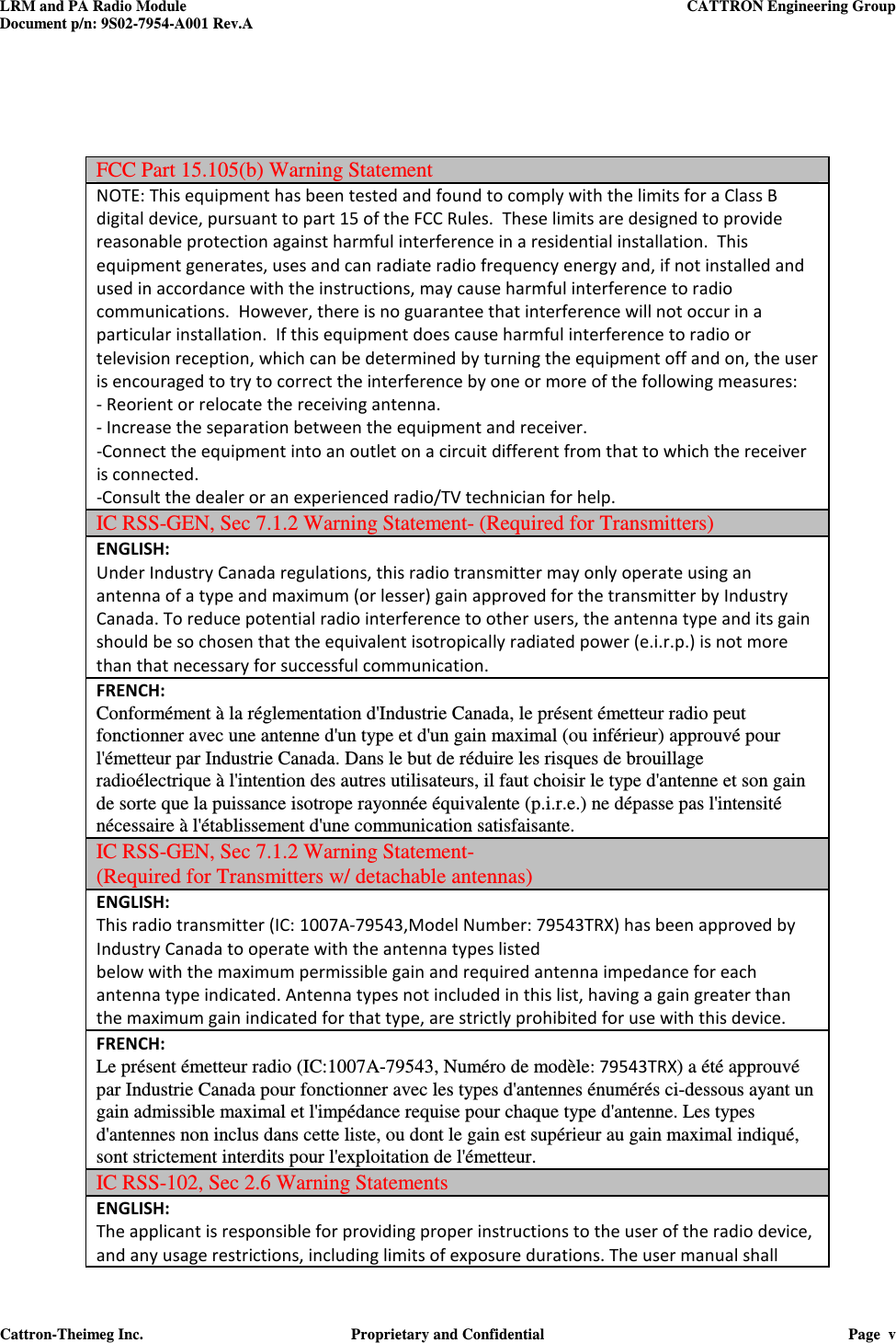
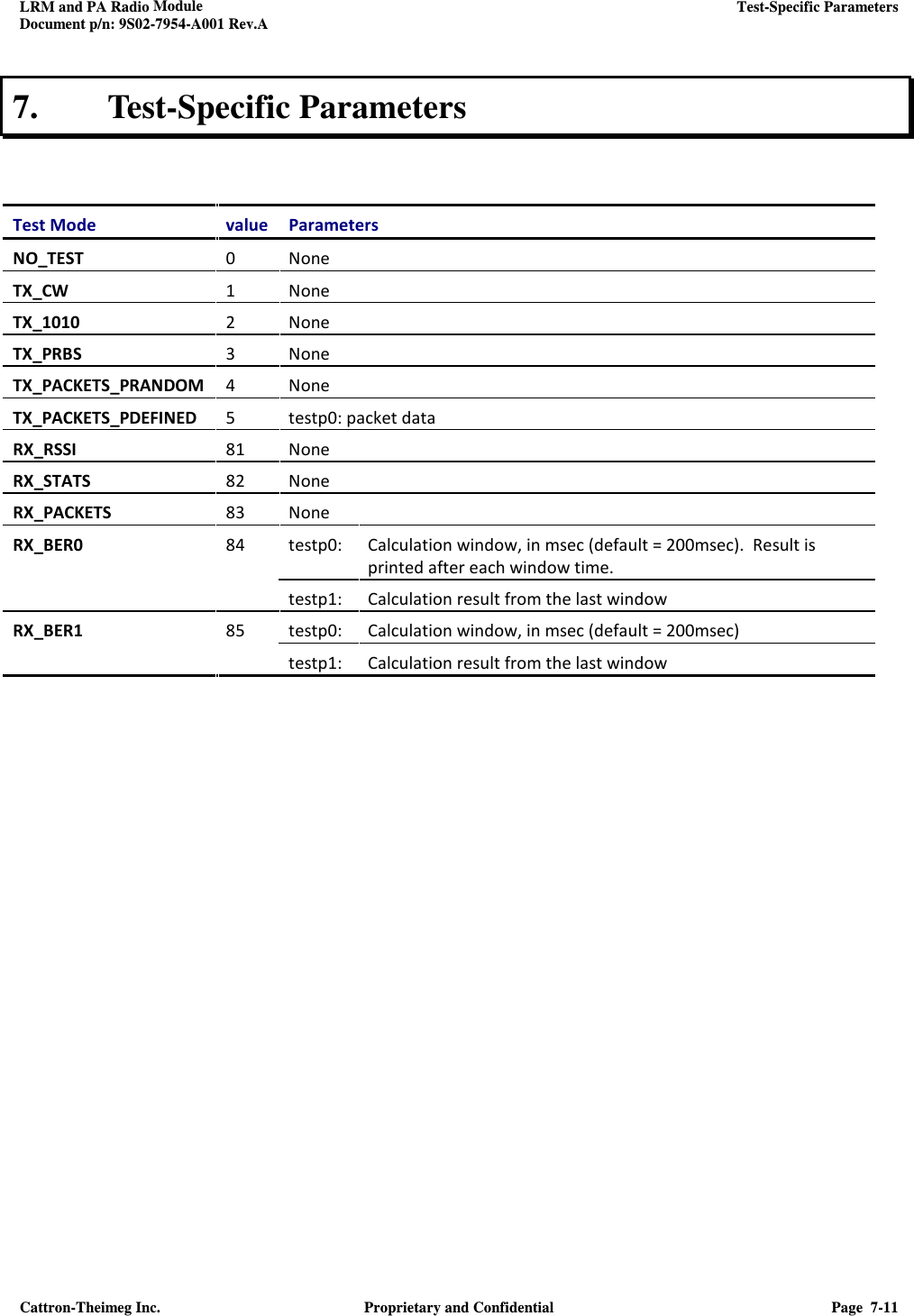
![LRM and PA Radio Module LRM Configuration Concept Document p/n: 9S02-7954-A001 Rev.A Cattron-Theimeg Inc. Proprietary and Confidential Page 4-4 4. LRM Configuration Concept All LRM configuration and status parameters are accessible through addressable registers. - All parameters can be read in any of the following state: IDLE, RX, TX - All writable parameters can be written in the following state: IDLE only In order to facilitate adaptation to different platforms, the LRM configuration registers can be accessed using anyone of three methods: I2C, SPI or serial asynchronous with ASCII strings. The definition of the configuration registers is given in reference [3]. This section addresses the basic description of all these three methods. 4.1 I2C Signals I2C_SDA and I2C_SCL are used, according to the I2C standard protocol. The LRM I2C configuration interface LRM emulates the behavior of the 1Kbytes I2C E2PROM found in all Unity RF modules. This way, I2C operation is consistent for all Unity radios. • Device Address: 0xA0 (same as other Unity RF modules) • Device select code: • Write operations: supports “Byte write” and “Page write”. • Read operations: supports “Random Address Read” and “Sequential Random Read”. For more details, refer to the M24C08 serial I2C E2PROM datasheet. 4.2 SPI Signals SPI_PDO, SPI_PDI, SPI_CLK and SPI_PLE are used. [TBD: Timings. (the LRM is a clock consumer)] 4.3 Console Interface The serial interface configuration port is enabled by asserting !CONFIG signal; the serial interface is automatically reconfigured in asynchronous mode, running at 38400bps, 8N1. All ASCII strings received are interpreted as configuration commands. This mode is particularly useful for stand-alone testing, when the unit can be controlled from a PC or by an operator/tester using a terminal emulation program. 4.3.1 “Write” command wrCmd register value , where: wrCmd = write command. w or wr can be used and are equivalent register = register identification. Can use the register name or register address value = value to be written, in decimal or hexadecimal format. Hexadecimal values are preceded by ‘0x’ Examples: wr txf 915000000 : Write 915000000 to register txf (Tx frequency)](https://usermanual.wiki/Cattron-North-America/79543-91072/User-Guide-2468461-Page-11.png)
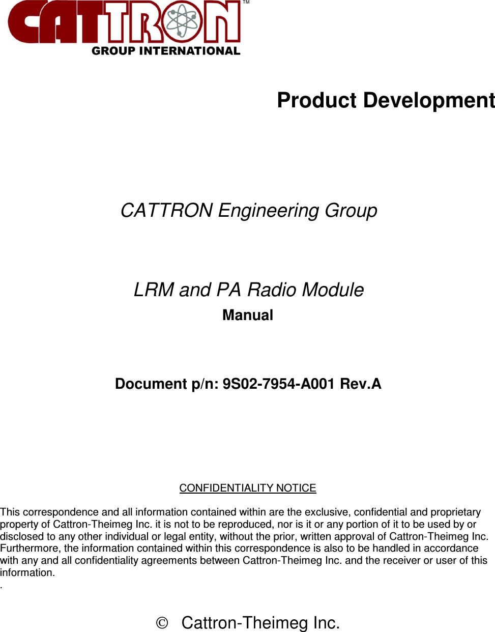
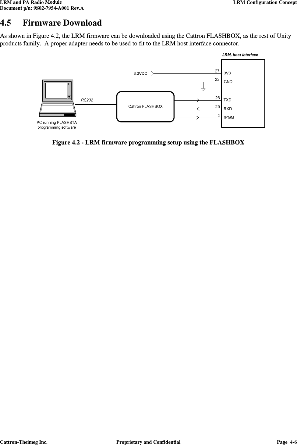
![LRM and PA Radio Module LRM Configuration Concept Document p/n: 9S02-7954-A001 Rev.A Cattron-Theimeg Inc. Proprietary and Confidential Page 4-5 wr 0x80 18 : Write 18 to register address 0x80 wr txf 915000000 0x80 18: Concatenate the two writes above in a single instruction 4.3.2 “Read” command rdCmd reg where: rdCmd= read command. r or rd can be used and are equivalent reg = register identification. Can use the register name or register address Examples: rd txf : Reads register txf (Tx frequency) rd 0x80 : Reads register address 0x80 rd txf 0x80 : Reads registers txf and 0x80 in a single instruction 4.4 Stand-Alone Test Mode The LRM can be operated in stand-alone mode for production/service tests. In this case, only a 3.3VDC supply is needed, and a RS232/TTL transceiver (like Cattron FLASHBOX) to connect to a PC serial port. Figure 4.1 - LRM connection for stand-alone operation The LRM will support several built-in test modes to ease testing from a PC. For example a. Transmission Tests - Generation of different type of carrier: unmodulated (CW), or modulated with “101010..” or pseudo-random sequence - Automatic generation of test RF frames with predefined content b. Reception Tests - Measure PER (packet error rate) when receiving the predefined test RF frames - Measure RF input level More details about the test modes can be found in reference [3].](https://usermanual.wiki/Cattron-North-America/79543-91072/User-Guide-2468461-Page-12.png)
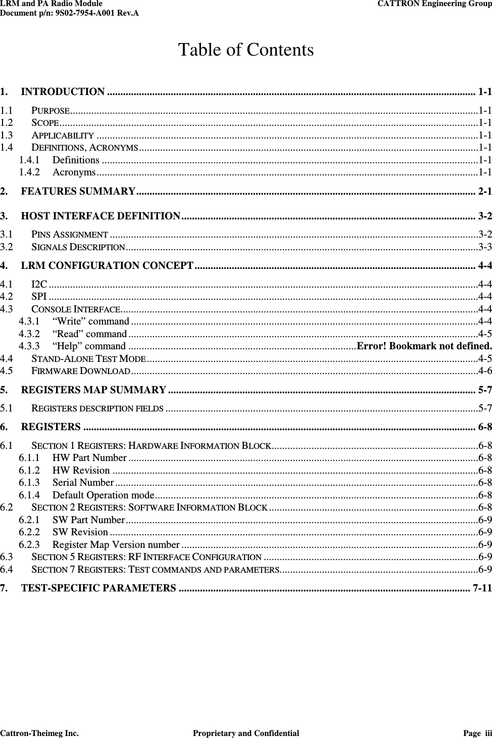
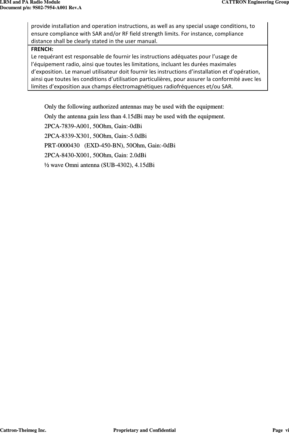
![LRM and PA Radio Module Registers Document p/n: 9S02-7954-A001 Rev.A Cattron-Theimeg Inc. Proprietary and Confidential Page 6-8 6. Registers 6.1 Section 1 Registers: Hardware Information Block Section 1: Hardware Information Block Addr Type Array Size Access Keyword Description Details 0x00 UINT8 1 RWP id RF module ID 0x04 CHAR 14 RWP hwpn HW Part Number 0x12 CHAR 4 RWP hwrev HW Revision 0x16 CHAR 16 RWP sn Serial Number 0x26 UINT8 26 RWP sp Spare Reserved for future usage. 0x40 UINT8 1 RWP cmdef Default operation mode 0x43 UINT16 1 RWP crc HIB CRC (Hardware Info Block) This section is formatted according the standard Unity RF modules E2PROM data format, described in reference [3]. Hardware Information Block registers are write-protected; writes operations are allowed after the proper key code has been written in the WP unlock key register 6.1.1 HW Part Number Hardware part number is a 14 characters ASCII string formatted according to Cattron standard part number format; [4 digits prefix]-[4 digits number]-[4 digits suffix]. Example: “2PCA-7954-A001” 6.1.2 HW Revision This field is a 4 characters ASCII representation of the HW Revision. Cattron hardware parts revision is composed of 2 segments. The first segment is made of one or two letters followed with one or two optional numerical digits. revision. Examples: “PP3”, “A” 6.1.3 Serial Number A 16 digits field is reserved for serial numbers. Serial numbers format is not predefined. 6.1.4 Default Operation mode Default value for the LRM operation mode. LRM operation modes are described in section 6. 6.2 Section 2 Registers: Software Information Block Section 2: Software Information Block Addr Type Array Size Access Keyword Description Details 0x46 CHAR 14 R swpn SW Part Number Section 3.2.1 0x54 CHAR 10 R swrev SW Revision Section 3.2.2 0x5E UINT16 1 R mapver Register map version Section 3.2.3](https://usermanual.wiki/Cattron-North-America/79543-91072/User-Guide-2468461-Page-15.png)
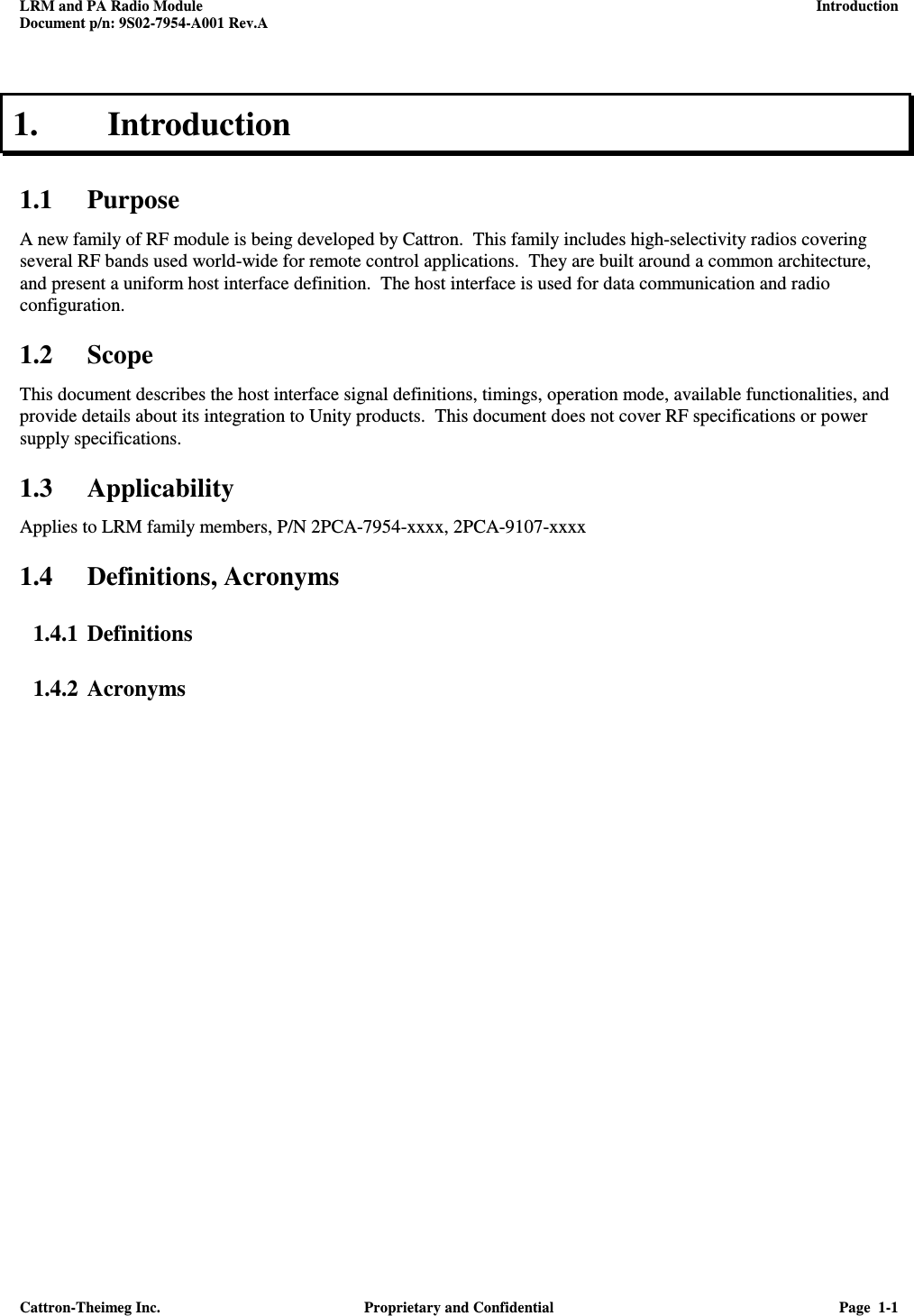
![LRM and PA Radio Module Registers Document p/n: 9S02-7954-A001 Rev.A Cattron-Theimeg Inc. Proprietary and Confidential Page 6-9 Software Information Block registers are read-only. 6.2.1 SW Part Number Software part number is a 14 characters ASCII string formatted according to Cattron standard part number format; [4 digits prefix]-[4 digits number]-[4 digits suffix]. Example: “3SOF-7954-A001” 6.2.2 SW Revision Software revision is given by 3 segments separated by commas. The segments are typically but not restricted to numbers. Ex: “3.12.7”, “1.2.7B”, A 10 characters long field is defined.. 6.2.3 Register Map Version number This is number is represented by numerical values. Ex: 1.34; - The second segment is incremented each time new registers are added to the Register map, and this addition has no impact on backward compatibility. It is encoded on in the LSB. - The first segment is incremented each time a change to the Register Map has any impact on backward compatibility. It is encoded in the MSB. For example, “1.34” would be encoded as 0x0122. 6.3 Section 5 Registers: RF Interface Configuration These parameters control the operation of the RF interface. Section 5: RF Interface Configuration Addr Type Array Size Access Keyword Description Details 0x80 UINT32 1 RW txf Tx Frequency (Hz) The new frequency is set at the next transition to Tx mode 0x84 UINT32 1 RW rxf Rx Frequency (Hz) The new frequency is set at the next transition to Rx mode 0x88 INT8 1 RW txp Tx Level(dBm) If the Tx level value is outside the range supported by the radio, the nearest supported value is set and readback. 0x8a INT8 1 R rssi Current RSSI (dBm) Reads current RSSI at frequency rxf. (Note: the LRM shall be in Rx mode) 0x8b INT8 1 R prssi RSSI of last received packet (dBm) 0x8c UINT8 1 RW psize Max size of received packets In number of bytes 6.4 Section 7 Registers: Test commands and parameters This section implements tests utilities that can be used for development, production and service.](https://usermanual.wiki/Cattron-North-America/79543-91072/User-Guide-2468461-Page-16.png)