Cattron North America 79546-91071 Wireless Remote Control Unit User Manual 9S02 7954 A001 FCC Manual
Laird Controls North America Inc. Wireless Remote Control Unit 9S02 7954 A001 FCC Manual
User Manual

Product Development
CATTRON Engineering Group
LRM and PA Radio Module
Manual
Document p/n: 9S02-7954-A001 Rev.A
CONFIDENTIALITY NOTICE
This correspondence and all information contained within are the exclusive, confidential and proprietary
property of Cattron-Theimeg Inc. it is not to be reproduced, nor is it or any portion of it to be used by or
disclosed to any other individual or legal entity, without the prior, written approval of Cattron-Theimeg Inc.
Furthermore, the information contained within this correspondence is also to be handled in accordance
with any and all confidentiality agreements between Cattron-Theimeg Inc. and the receiver or user of this
information.
.
Cattron-Theimeg Inc.

LRM and PA Radio Module CATTRON Engineering Group
Document p/n: 9S02-7954-A001 Rev.A
Cattron-Theimeg Inc. Proprietary and Confidential Page ii
Revision History
Date Revision Description Signature / Date
2010-10-06
EM1 Initial draft Prepared Pierre Montreuil
Verified
Approved
2010-10-06
EM2 General revision.
Removed LQI measurement
Updated the configuration section (section 5)
Prepared Pierre Montreuil
Verified
Approved
2012-01-30
A Fig 4.8 and 4.9 - Remove remaining references to LQI from
drawings.
Table 4.2 – Rename ESC_END for ESC_SOF
[LaB] Added demodulated analog output on pin 48 and
GND on pin 50
Prepared Pierre Montreuil
Verified
Approved
Prepared
Verified
Approved
LRM and PA Radio Module CATTRON Engineering Group
Document p/n: 9S02-7954-A001 Rev.A
Cattron-Theimeg Inc. Proprietary and Confidential Page iii
Table of Contents
1.
INTRODUCTION ........................................................................................................................................... 1-1
1.1
PURPOSE ..........................................................................................................................................................1-1
1.2
SCOPE ..............................................................................................................................................................1-1
1.3
APPLICABILITY ................................................................................................................................................1-1
1.4
DEFINITIONS, ACRONYMS ................................................................................................................................1-1
1.4.1
Definitions ..............................................................................................................................................1-1
1.4.2
Acronyms ................................................................................................................................................1-1
2.
FEATURES SUMMARY ................................................................................................................................ 2-1
3.
HOST INTERFACE DEFINITION ............................................................................................................... 3-2
3.1
PINS ASSIGNMENT ...........................................................................................................................................3-2
3.2
SIGNALS DESCRIPTION .....................................................................................................................................3-3
4.
LRM CONFIGURATION CONCEPT .......................................................................................................... 4-4
4.1
I2C ..................................................................................................................................................................4-4
4.2
SPI ..................................................................................................................................................................4-4
4.3
CONSOLE INTERFACE.......................................................................................................................................4-4
4.3.1
“Write” command ...................................................................................................................................4-4
4.3.2
“Read” command ....................................................................................................................................4-5
4.3.3
“Help” command ...................................................................................... Error! Bookmark not defined.
4.4
STAND-ALONE TEST MODE .............................................................................................................................4-5
4.5
FIRMWARE DOWNLOAD ...................................................................................................................................4-6
5.
REGISTERS MAP SUMMARY .................................................................................................................... 5-7
5.1
REGISTERS DESCRIPTION FIELDS ......................................................................................................................5-7
6.
REGISTERS .................................................................................................................................................... 6-8
6.1
SECTION 1 REGISTERS: HARDWARE INFORMATION BLOCK ..............................................................................6-8
6.1.1
HW Part Number ....................................................................................................................................6-8
6.1.2
HW Revision ..........................................................................................................................................6-8
6.1.3
Serial Number .........................................................................................................................................6-8
6.1.4
Default Operation mode ..........................................................................................................................6-8
6.2
SECTION 2 REGISTERS: SOFTWARE INFORMATION BLOCK ...............................................................................6-8
6.2.1
SW Part Number .....................................................................................................................................6-9
6.2.2
SW Revision ...........................................................................................................................................6-9
6.2.3
Register Map Version number ................................................................................................................6-9
6.3
SECTION 5 REGISTERS: RF INTERFACE CONFIGURATION .................................................................................6-9
6.4
SECTION 7 REGISTERS: TEST COMMANDS AND PARAMETERS...........................................................................6-9
7.
TEST-SPECIFIC PARAMETERS .............................................................................................................. 7-11

LRM and PA Radio Module CATTRON Engineering Group
Document p/n: 9S02-7954-A001 Rev.A
Cattron-Theimeg Inc. Proprietary and Confidential Page iv
79546+91071 TRX module meets Part 90 of the FCC rules and regulations. Compliance with the
labeling requirements, FCC notices is required. In order to comply with FCC Certification
requirements, the Original Equipment Manufacturer (OEM) must fulfill the following requirements.
1. The system integrator must place an exterior label on the outside of the final product
housing the 79546+91071TRX Module. The figure below shows the contents that must be
included in this label.
2. 79546+91071 TRX modules may only be used with the antennas that have been
tested and approved for use with the module.
Labeling Requirements
The OEM must make sure that FCC labeling requirements are met. This includes a clearly visible
exterior label on the outside of the final product housing that displays the contents shown in
below.
WARNING: The 79546+91071 TRX modules have been tested by the FCC for use with other products
without further certification (as per FCC Section 2.1091). Changes or modifications to this device not
expressly approved by Cattron-Theimeg could void the user’s authority to operate the equipment.
NOTICE: OEM’s must verify the final end product complies with unintentional radiators (FCC Section
15.107 and 15.109) before providing a declaration of conformity for their final product to Part 15 of the
FCC Rules.
NOTICE: The 79546+91071 TRX modules have been certified for mobile and fixed radio
applications. If the module will be used for portable applications, the device must undergo SAR
testing.
RF Exposure WARNING: This equipment complies with FCC radiation exposure limits set forth for an
uncontrolled environment. This equipment should be installed and operated with minimum distance 20
cm between the radiator and your body. This transmitter must not be co-located or operating in
conjunction with any other antenna or transmitter.
NOTICE: The preceding statement must be included as a CAUTION statement in OEM product
manuals in order to alert users of FCC RF Exposure compliance.
79546+91071 TRX is designed for use in countless wireless applications requiring long range
communications with low energy consumption. To ensure that the final product complies with the all of
the regulatory requirements for the Modular Grant the following integration instructions should be
followed. 79546+91071 TRX is limited to OEM installation ONLY. The OEM integrator is responsible
for ensuring that the end-user has no manual instructions to remove or install the module.

LRM and PA Radio Module CATTRON Engineering Group
Document p/n: 9S02-7954-A001 Rev.A
Cattron-Theimeg Inc. Proprietary and Confidential Page v
FCC Part 15.105(b) Warning Statement
NOTE: This equipment has been tested and found to comply with the limits for a Class B
digital device, pursuant to part 15 of the FCC Rules. These limits are designed to provide
reasonable protection against harmful interference in a residential installation. This
equipment generates, uses and can radiate radio frequency energy and, if not installed and
used in accordance with the instructions, may cause harmful interference to radio
communications. However, there is no guarantee that interference will not occur in a
particular installation. If this equipment does cause harmful interference to radio or
television reception, which can be determined by turning the equipment off and on, the user
is encouraged to try to correct the interference by one or more of the following measures:
- Reorient or relocate the receiving antenna.
- Increase the separation between the equipment and receiver.
-Connect the equipment into an outlet on a circuit different from that to which the receiver
is connected.
-Consult the dealer or an experienced radio/TV technician for help.
IC RSS-GEN, Sec 7.1.2 Warning Statement- (Required for Transmitters)
ENGLISH:
Under Industry Canada regulations, this radio transmitter may only operate using an
antenna of a type and maximum (or lesser) gain approved for the transmitter by Industry
Canada. To reduce potential radio interference to other users, the antenna type and its gain
should be so chosen that the equivalent isotropically radiated power (e.i.r.p.) is not more
than that necessary for successful communication.
FRENCH:
Conformément à la réglementation d'Industrie Canada, le présent émetteur radio peut
fonctionner avec une antenne d'un type et d'un gain maximal (ou inférieur) approuvé pour
l'émetteur par Industrie Canada. Dans le but de réduire les risques de brouillage
radioélectrique à l'intention des autres utilisateurs, il faut choisir le type d'antenne et son gain
de sorte que la puissance isotrope rayonnée équivalente (p.i.r.e.) ne dépasse pas l'intensité
nécessaire à l'établissement d'une communication satisfaisante.
IC RSS-GEN, Sec 7.1.2 Warning Statement-
(Required for Transmitters w/ detachable antennas)
ENGLISH:
This radio transmitter (IC: 1007A-79543,Model Number: 79543TRX) has been approved by
Industry Canada to operate with the antenna types listed
below with the maximum permissible gain and required antenna impedance for each
antenna type indicated. Antenna types not included in this list, having a gain greater than
the maximum gain indicated for that type, are strictly prohibited for use with this device.
FRENCH:
Le présent émetteur radio (IC:1007A-79543, Numéro de modèle: 79543TRX) a été approuvé
par Industrie Canada pour fonctionner avec les types d'antennes énumérés ci-dessous ayant un
gain admissible maximal et l'impédance requise pour chaque type d'antenne. Les types
d'antennes non inclus dans cette liste, ou dont le gain est supérieur au gain maximal indiqué,
sont strictement interdits pour l'exploitation de l'émetteur.
IC RSS-102, Sec 2.6 Warning Statements
ENGLISH:
The applicant is responsible for providing proper instructions to the user of the radio device,
and any usage restrictions, including limits of exposure durations. The user manual shall

LRM and PA Radio Module CATTRON Engineering Group
Document p/n: 9S02-7954-A001 Rev.A
Cattron-Theimeg Inc. Proprietary and Confidential Page vi
provide installation and operation instructions, as well as any special usage conditions, to
ensure compliance with SAR and/or RF field strength limits. For instance, compliance
distance shall be clearly stated in the user manual.
FRENCH:
Le requérant est responsable de fournir les instructions adéquates pour l’usage de
l’équipement radio, ainsi que toutes les limitations, incluant les durées maximales
d’exposition. Le manuel utilisateur doit fournir les instructions d’installation et d’opération,
ainsi que toutes les conditions d’utilisation particulières, pour assurer la conformité avec les
limites d’exposition aux champs électromagnétiques radiofréquences et/ou SAR.
Only the following authorized antennas may be used with the equipment:
Or the antenna gain less than 5.15dBi may be used with the equipment.
PRT-0000092 (whip antenna SPHS24221), 50Ohm, Gain: 0dBi
PRT-0000098 (whip antenna SPHS24221), 50Ohm, Gain: 0dBi
2PCA-8467-X001(Helical Antenna), 50Ohm, Gain: -8dBi
½ wave Omni antenna (ASPH7455), 5.15dBi

LRM and PA Radio Module Introduction
Document p/n: 9S02-7954-A001 Rev.A
Cattron-Theimeg Inc. Proprietary and Confidential Page 1-1
1. Introduction
1.1 Purpose
A new family of RF module is being developed by Cattron. This family includes high-selectivity radios covering
several RF bands used world-wide for remote control applications. They are built around a common architecture,
and present a uniform host interface definition. The host interface is used for data communication and radio
configuration.
1.2 Scope
This document describes the host interface signal definitions, timings, operation mode, available functionalities, and
provide details about its integration to Unity products. This document does not cover RF specifications or power
supply specifications.
1.3 Applicability
Applies to LRM family members, P/N 2PCA-7954-xxxx, 2PCA-9107-xxxx
1.4 Definitions, Acronyms
1.4.1 Definitions
1.4.2 Acronyms

LRM and PA Radio Module Features Summary
Document p/n: 9S02-7954-A001 Rev.A
Cattron-Theimeg Inc. Proprietary and Confidential Page 2-1
2. Features Summary
The LRM design addresses in first place Unity applications requirements. Its interface however is general enough to
allow compatibility to other legacy Cattron products.
• Direct electrical compatibility to Unity RF interface – The interface is defined for natural integration to Unity
product line.
• On-board CPU – The interface is controlled by an on-board Renesas CPU. This CPU controls also the details of
operation of the RF peripherals. This approach has several advantages:
a. Unified host interface definition – A single host interface can be defined for all LRM family members.
b. Low requirement on Host CPU resources – The on-board CPU takes care of most aspects of RF control and
timings. This allows releasing CPU resources (processing time, ROM/RAM space, hardware timers) that
become available for more features addition.
c. Simple Host device drivers - Most of driver firmware complexity is transferred on the radio CPU; the Host
device driver is much simpler, easier to test, and not as critical in regard to timings.
• Several interface modes – Several interface modes are supported in order to allow integration with other Cattron
legacy products:
a. Data interface - support for synchronous and asynchronous serial link.
b. Configuration interface - support for I2C, SPI and asynchronous serial access.
• Stand-alone operation for firmware download and production test – The LRM can interface almost directly to a
PC serial port for firmware download and for testing (no need for CPU board); only a TTL/RS232 translator is
required (such as Cattron flashbox).
• Support for advanced feature – The LRM family is designed to support advanced features such as FHSS
(Frequency Hopping Spread Spectrum) and Adaptive Channel Allocation, with minimal impact on Host
firmware.
These different aspects are covered in the rest of this document.
LRM and PA Radio Module Host Interface Definition
Document p/n: 9S02-7954-A001 Rev.A
Cattron-Theimeg Inc. Proprietary and Confidential Page 3-2
3. Host Interface Definition
3.1 Pins Assignment
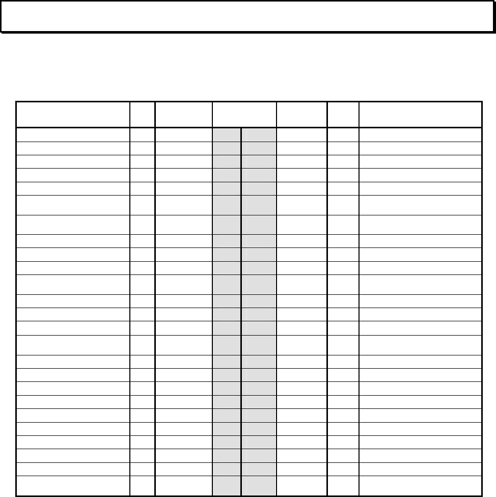
Description IO Signal Pin
Number Signal IO Description
49 50 GND Ground
47 48 RX_BB O RX Baseband signal
45 46
43 44
41 42
I2C clock /
SPI clock
IO/
O
I2C_SCL /
SPI_SCK 39 40 SPI_PLE I SPI Strobe
SPI data input I SPI_PDI 37 38 I2C_SDA /
SPI_PDO
IO /
O
I2C Data /
SPI data output
35 36
33 34
31 32
Data transfer Handshaking
Signal O !READY 29 30
3.3V DC supply I 3V3 27 28
Receive data O RXD 25 26 TXD I Transmit Data
RX Enable I !RX_EN 23 24 !TX_EN I Tx Enable
Serial port Configuration
mode I !CONFIG 21 22 GND Ground
19 20 DCLK O Data Clock
17 18
15 16
13 14
11 12
9 10
Reset I !RESET 7 8
CPU flash mode I !PGM 5 6
Ground GND-PA 3 4 GND-PA Ground
Voltage Supply, RF power
amplifier I VPA 1 2 VPA I Voltage Supply, RF power
amplifier
Table 3.1 – Host Interface pins assignment

LRM and PA Radio Module Host Interface Definition
Document p/n: 9S02-7954-A001 Rev.A
Cattron-Theimeg Inc. Proprietary and Confidential Page 3-3
3.2 Signals Description
Pin
Nb
Signal
Name
I/O Description Category
1, 2 VPA Input Voltage Supply, RF power amplifier.
This supply is needed when an optional piggy-back power amplifier board is
used. Specifications (voltage, current) depend on piggy-back board used.
Power supply
3, 4 GND-PA GND, RF power amplifier.
This ground is connected internally to the module ground. It does not need to
be connected when the module is used without PA
Power supply
22, 50 GND System ground Power supply
27 3V3 Input 3.3 V power supply voltage input (Vcc) Power supply
5 !PGM Input Used to download on-board CPU firmware. Connect this signal to GND at
power-up to force the CPU to enter firmware programming mode. Otherwise,
connect to Vcc or leave unconnected
Module control
7 !RESET Input Main reset (active low). When reset is asserted, the content of the internal
registers is lost.
Module control
29 !READY Output Handshaking signal for transmit or receive data on the host interface. Data
Transmission
23 !RX_EN Input Receive Enable (active low). Used to place the RF module in received mode
*Note: when !TX_EN and !RX_EN are asserted simultaneously, the module is
placed in STANDBY mode (low power consumption, internal registers
conservation)
Data
Transmission
24 !TX_EN Input Transmit Enable (active low). Used to activate telegram transmit process Data
Transmission
25 RXD Output Receive Data. Data
Transmission
26 TXD Input Transmit Data Data
Transmission
20 DCLK Output Data Clock. Active when serial port is configured in Synchronous Mode Data
Transmission
21 !CONFIG Input Used to configure the Data transmission signals RXD and TXD for module
configuration.
Asserting can be done in IDLE state only. Active low
Configuration
interface
37 SPI_PDI Input If configuration interface configured for SPI: PDI (Peripheral Data In) Configuration
interface
38 I2C_SDA
SPI_PDO
Bidi /
Output
If configuration interface configured for:
I2C: I2C SDA signal (data)
SPI: PDO (Peripheral Data Out)
Configuration
interface
39 I2C_SCL
SPI_SCLK
Bidi /
Input
If configuration interface configured for:
I2C: I2C SCL signal (clock)
SPI: SCLK (Serial Clock)
Configuration
interface
40 SPI_PLE Input If configuration interface is configured for SPI
PLE: (Peripheral Data Load Enable)
Configuration
interface
48 RX_BB Output Analog demodulated RX signal Data
Transmission
Table 3.2 - Host Interface signals description
LRM and PA Radio Module LRM Configuration Concept
Document p/n: 9S02-7954-A001 Rev.A
Cattron-Theimeg Inc. Proprietary and Confidential Page 4-4
4. LRM Configuration Concept
All LRM configuration and status parameters are accessible through addressable registers.
- All parameters can be read in any of the following state: IDLE, RX, TX
- All writable parameters can be written in the following state: IDLE only
In order to facilitate adaptation to different platforms, the LRM configuration registers can be accessed using anyone
of three methods: I2C, SPI or serial asynchronous with ASCII strings.
The definition of the configuration registers is given in reference [3]. This section addresses the basic description of
all these three methods.
4.1 I2C
Signals I2C_SDA and I2C_SCL are used, according to the I2C standard protocol.
The LRM I2C configuration interface LRM emulates the behavior of the 1Kbytes I2C E2PROM found in all Unity
RF modules. This way, I2C operation is consistent for all Unity radios.
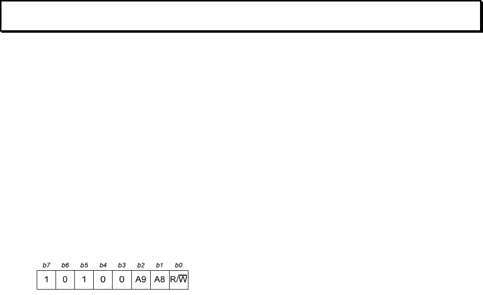
• Device Address: 0xA0 (same as other Unity RF modules)
• Device select code:
• Write operations: supports “Byte write” and “Page write”.
• Read operations: supports “Random Address Read” and “Sequential Random Read”.
For more details, refer to the M24C08 serial I2C E2PROM datasheet.
4.2 SPI
Signals SPI_PDO, SPI_PDI, SPI_CLK and SPI_PLE are used.
[TBD: Timings. (the LRM is a clock consumer)]
4.3 Console Interface
The serial interface configuration port is enabled by asserting !CONFIG signal; the serial interface is automatically
reconfigured in asynchronous mode, running at 38400bps, 8N1. All ASCII strings received are interpreted as
configuration commands. This mode is particularly useful for stand-alone testing, when the unit can be controlled
from a PC or by an operator/tester using a terminal emulation program.
4.3.1 “Write” command
wrCmd register value , where:
wrCmd = write command. w or wr can be used and are equivalent
register = register identification. Can use the register name or register address
value = value to be written, in decimal or hexadecimal format. Hexadecimal values are preceded by ‘0x’
Examples:
wr txf 915000000 : Write 915000000 to register txf (Tx frequency)
LRM and PA Radio Module LRM Configuration Concept
Document p/n: 9S02-7954-A001 Rev.A
Cattron-Theimeg Inc. Proprietary and Confidential Page 4-5
wr 0x80 18 : Write 18 to register address 0x80
wr txf 915000000 0x80 18: Concatenate the two writes above in a single instruction
4.3.2 “Read” command
rdCmd reg where:
rdCmd= read command. r or rd can be used and are equivalent
reg = register identification. Can use the register name or register address
Examples:
rd txf : Reads register txf (Tx frequency)
rd 0x80 : Reads register address 0x80
rd txf 0x80 : Reads registers txf and 0x80 in a single instruction
4.4 Stand-Alone Test Mode
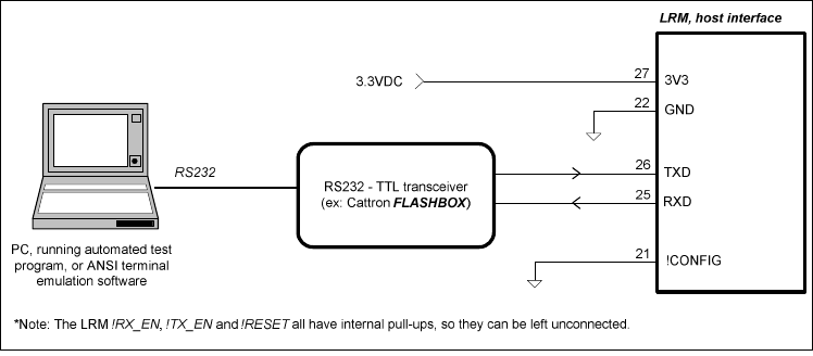
The LRM can be operated in stand-alone mode for production/service tests. In this case, only a 3.3VDC supply is
needed, and a RS232/TTL transceiver (like Cattron FLASHBOX) to connect to a PC serial port.
Figure 4.1 - LRM connection for stand-alone operation
The LRM will support several built-in test modes to ease testing from a PC. For example
a. Transmission Tests
- Generation of different type of carrier: unmodulated (CW), or modulated with “101010..” or pseudo-random
sequence
- Automatic generation of test RF frames with predefined content
b. Reception Tests
- Measure PER (packet error rate) when receiving the predefined test RF frames
- Measure RF input level
More details about the test modes can be found in reference [3].
LRM and PA Radio Module LRM Configuration Concept
Document p/n: 9S02-7954-A001 Rev.A
Cattron-Theimeg Inc. Proprietary and Confidential Page 4-6
4.5 Firmware Download
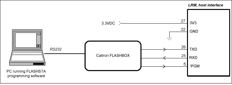
As shown in Figure 4.2, the LRM firmware can be downloaded using the Cattron FLASHBOX, as the rest of Unity
products family. A proper adapter needs to be used to fit to the LRM host interface connector.
Figure 4.2 - LRM firmware programming setup using the FLASHBOX

LRM and PA Radio Module Registers Map Summary
Document p/n: 9S02-7954-A001 Rev.A
Cattron-Theimeg Inc. Proprietary and Confidential Page 5-7
5. Registers Map Summary
5.1 Registers description fields
The registers are specified by the following parameters
1. Register address: This address can be used from the console, I2C or SPI accesses.
2. Parameter type:
TYPE Description
BOOL Boolean value: 0 or 1
UINT8 8 bits value, unsigned
INT8 8 bits value, signed
UINT16 16 bits value, unsigned
INT16 16 bits value, signed
UINT32 32 bits value, unsigned
INT32 32 bits value, signed
CHAR ASCII-encoded character
3. Array Size: Number of instances of this register. Each instance is referred to by using the keyword appended
with the instance number. Ex: reg0, reg1, reg2, ….
4. Access Type:
Access Type Description
R Read only
RW Read/Write
WP Write-protected
RWP Read/Write-protected
“Write protected” registers cannot be written, unless the correct key code has been written in the WP unlock key
register.
5. Keyword: keyword use for console access
6. Description: description printed on the console after a help command.
LRM and PA Radio Module Registers
Document p/n: 9S02-7954-A001 Rev.A
Cattron-Theimeg Inc. Proprietary and Confidential Page 6-8
6. Registers
6.1 Section 1 Registers: Hardware Information Block
Section 1: Hardware Information Block
Addr Type Array
Size
Access Keyword Description Details
0x00 UINT8 1 RWP id RF module ID
0x04 CHAR 14 RWP hwpn HW Part Number
0x12 CHAR 4 RWP hwrev HW Revision
0x16 CHAR 16 RWP sn Serial Number
0x26 UINT8 26 RWP sp Spare Reserved for future usage.
0x40 UINT8 1 RWP cmdef Default operation mode
0x43 UINT16 1 RWP crc HIB CRC (Hardware Info Block)
This section is formatted according the standard Unity RF modules E2PROM data format, described in reference [3].
Hardware Information Block registers are write-protected; writes operations are allowed after the proper key code
has been written in the WP unlock key register
6.1.1 HW Part Number
Hardware part number is a 14 characters ASCII string formatted according to Cattron standard part number format;
[4 digits prefix]-[4 digits number]-[4 digits suffix]. Example: “2PCA-7954-A001”
6.1.2 HW Revision
This field is a 4 characters ASCII representation of the HW Revision. Cattron hardware parts revision is composed
of 2 segments. The first segment is made of one or two letters followed with one or two optional numerical digits.
revision. Examples: “PP3”, “A”
6.1.3 Serial Number
A 16 digits field is reserved for serial numbers. Serial numbers format is not predefined.
6.1.4 Default Operation mode
Default value for the LRM operation mode. LRM operation modes are described in section 6.
6.2 Section 2 Registers: Software Information Block
Section 2: Software Information Block
Addr Type Array
Size
Access Keyword Description Details
0x46 CHAR 14 R swpn SW Part Number Section 3.2.1
0x54 CHAR 10 R swrev SW Revision Section 3.2.2
0x5E UINT16 1 R mapver Register map version Section 3.2.3

LRM and PA Radio Module Registers
Document p/n: 9S02-7954-A001 Rev.A
Cattron-Theimeg Inc. Proprietary and Confidential Page 6-9
Software Information Block registers are read-only.
6.2.1 SW Part Number
Software part number is a 14 characters ASCII string formatted according to Cattron standard part number format;
[4 digits prefix]-[4 digits number]-[4 digits suffix]. Example: “3SOF-7954-A001”
6.2.2 SW Revision
Software revision is given by 3 segments separated by commas. The segments are typically but not restricted to
numbers. Ex: “3.12.7”, “1.2.7B”,
A 10 characters long field is defined..
6.2.3 Register Map Version number
This is number is represented by numerical values. Ex: 1.34;
- The second segment is incremented each time new registers are added to the Register map, and this addition has
no impact on backward compatibility. It is encoded on in the LSB.
- The first segment is incremented each time a change to the Register Map has any impact on backward
compatibility. It is encoded in the MSB.
For example, “1.34” would be encoded as 0x0122.
6.3 Section 5 Registers: RF Interface Configuration
These parameters control the operation of the RF interface.
Section 5: RF Interface Configuration
Addr Type Array
Size
Access Keyword Description Details
0x80 UINT32 1 RW txf Tx Frequency (Hz) The new frequency is set at the next transition to
Tx mode
0x84 UINT32 1 RW rxf Rx Frequency (Hz) The new frequency is set at the next transition to
Rx mode
0x88 INT8 1 RW txp Tx Level(dBm) If the Tx level value is outside the range supported
by the radio, the nearest supported value is set and
readback.
0x8a INT8 1 R rssi Current RSSI (dBm) Reads current RSSI at frequency rxf. (Note: the
LRM shall be in Rx mode)
0x8b INT8 1 R prssi RSSI of last received packet
(dBm)
0x8c UINT8 1 RW psize Max size of received packets In number of bytes
6.4 Section 7 Registers: Test commands and parameters
This section implements tests utilities that can be used for development, production and service.

LRM and PA Radio Module Registers
Document p/n: 9S02-7954-A001 Rev.A
Cattron-Theimeg Inc. Proprietary and Confidential Page 6-10
Section 7: Test Commands and Parameters
- Registers content after system reset is zero
Addr Type Size Access Keyword Description Details
0xe0 UINT8 1 W test Test Mode
0xe4 UINT32 7 RW testp Test Parameters

LRM and PA Radio Module Test-Specific Parameters
Document p/n: 9S02-7954-A001 Rev.A
Cattron-Theimeg Inc. Proprietary and Confidential Page 7-11
7. Test-Specific Parameters
Test Mode value Parameters
NO_TEST 0 None
TX_CW 1 None
TX_1010 2 None
TX_PRBS 3 None
TX_PACKETS_PRANDOM 4 None
TX_PACKETS_PDEFINED 5 testp0: packet data
RX_RSSI 81 None
RX_STATS 82 None
RX_PACKETS 83 None
RX_BER0 84 testp0: Calculation window, in msec (default = 200msec). Result is
printed after each window time.
testp1: Calculation result from the last window
RX_BER1 85 testp0: Calculation window, in msec (default = 200msec)
testp1: Calculation result from the last window