Cervis MRF450 LongRT Radio User Manual U077 0 2 MRF450 x
Cervis Inc. LongRT Radio U077 0 2 MRF450 x
Cervis >
Users Manual

2014 Cervis, Inc.
MRF450 User Manual
U077.0.2-MRF450
™

Module RF450
This document is the property of Cervis, Inc. and cannot be copied, modified, e-mailed, or reproduced
without the express prior written consent of Cervis, Inc.
Cervis, Inc. reserves the right to change this manual or edit, delete, or modify any information without prior
notification.
Operation of this module in Periodic Transmit mode requires a license.
FCC Statements
15.19 – Two Part Warning
This device complies with Part 15 of the FCC rules. Operation is subject to the following two conditions:
(1) This device may not cause harmful interference and
(2) This device must accept any interference received, including interference that may cause undesired operation.
15.21 – Unauthorized Modification
NOTICE: The manufacturer is not responsible for any unauthorized modifications to this equipment made by the user. Such modifications could void the
user’s authority to operate the equipment.
15.27 – Special Accessories
This device is supplied with special accessories that include an RF adapter cable and antenna. These special accessories must be used with the device. It is
the responsibility of the user to use the needed special accessories supplied with the equipment.
15.105(b) – Note:
This equipment has been tested and found to comply with the limits for a Class A digital device, pursuant to part 15 of the FCC Rules. These limits are
designed to provide reasonable protection against harmful interference when the equipment is operated in a commercial environment. This equipment
generates, uses, and can radiate radio frequency energy and, if not installed and used in accordance with the instruction manual, may cause harmful
interference to radio communications. Operation of this equipment in a residential area is likely to cause harmful interference in which case the user will be
required to correct the interference at his own expense.
Industry Canada Statements
RSS-GEN 7.1.2 – Transmitter Antenna / Antenne de L'émetteur
Under Industry Canada regulations, this radio transmitter may only operate using an antenna of a type and maximum (or lesser) gain approved for the
transmitter by Industry Canada. To reduce potential radio interference to other users, the antenna type and its gain should be so chosen that the equivalent
isotropically radiated power (e.i.r.p.) is not more than that necessary for successful communication.
Conformément à la réglementation d'Industrie Canada, le présent émetteur radio peut fonctionner avec une antenne d'un type et d'un gain maximal (ou
inférieur) approuvé pour l'émetteur par Industrie Canada. Dans le but de réduire les risques de brouillage radioélectrique à l'intention des autres utilisateurs, il
faut choisir le type d'antenne et son gain de sorte que la puissance isotrope rayonnée équivalente (p.i.r.e.) ne dépasse pas l'intensité nécessaire à
l'établissement d'une communication satisfaisante.
This radio transmitter 7955A-MRF450 has been approved by Industry Canada to operate with the antenna types listed below with the maximum permissible
gain and required antenna impedance for each antenna type indicated. Antenna types not included in this list, having a gain greater than the maximum gain
indicated for that type, are strictly prohibited for use with this device.
Le présent émetteur radio 7955A-MRF450 a été approuvé par Industrie Canada pour fonctionner avec les types d'antenne énumérés ci-dessous et ayant un
gain admissible maximal et l'impédance requise pour chaque type d'antenne. Les types d'antenne non inclus dans cette liste, ou dont le gain est supérieur au
gain maximal indiqué, sont strictement interdits pour l'exploitation de l'émetteur.
Approved Antenna List / Liste Antenne Approuvé
Manufacturer Part Number Gain Impedance
Nearson L324TR-440 0 dBi 50 Ohm
RSS-GEN 7.1.3 – Notice / Délai
This device complies with Industry Canada licence-exempt RSS standard(s). Operation is subject to the following two conditions: (1) this device may not cause
interference, and (2) this device must accept any interference, including interference that may cause undesired operation of the device.
Le présent appareil est conforme aux CNR d'Industrie Canada applicables aux appareils radio exempts de licence. L'exploitation est autorisée aux deux
conditions suivantes : (1) l'appareil ne doit pas produire de brouillage, et (2) l'utilisateur de l'appareil doit accepter tout brouillage radioélectrique subi, même si
le brouillage est susceptible d'en compromettre le fonctionnement.

User Manual
2014 Cervis, Inc. i
Table of Contents
Table of Contents .......................................................................................................................... i
List of Figures ............................................................................................................................... i
List of Tables ................................................................................................................................. i
Cervis Inc. Safety Precautions ................................................................................................... 1
1.0Introduction .......................................................................................................................... 2
1.1Features ............................................................................................................................. 2
1.2Dimensions (mils)/Locations ........................................................................................... 3
1.3Pinout ................................................................................................................................. 3
2.0Installation ............................................................................................................................ 4
3.0Tune-up Procedure .............................................................................................................. 4
4.0Electrical Characteristics .................................................................................................... 5
4.1Power ................................................................................................................................. 5
4.2SPI Mode ............................................................................................................................ 5
4.3UART Mode ........................................................................................................................ 5
5.0RF Characteristics ............................................................................................................... 6
6.0Operational Modes ............................................................................................................... 7
6.1Push-To-Transmit Mode ................................................................................................... 7
6.2Periodic Transmit Mode ................................................................................................... 7
7.0Communication Protocol .................................................................................................... 8
7.1SPI ...................................................................................................................................... 8
7.2UART .................................................................................................................................. 8
7.3Acknowledgement ............................................................................................................ 9
8.0Messages ............................................................................................................................ 10
8.1Get / Set Parameter ......................................................................................................... 10
8.2Transmit ........................................................................................................................... 12
8.3Receive ............................................................................................................................ 13
8.4Error ................................................................................................................................. 14
List of Figures
Figure 1. MRF450 Front and Back ................................................................................................ 2
Figure 2. Dimensions (mils)/Locations ........................................................................................ 3
Figure 3. State Transitions vs. Current Consumption................................................................ 5
List of Tables
Table 1. P1, P2, and P3 Pinout ...................................................................................................... 3
Table 2. Recommended Baud Rates and Associated Deviation ............................................... 6
Table 3. OTA Structure Format ..................................................................................................... 6
Table 4. Packet Format Diagram................................................................................................... 8
Table 5. Message IDs and Structures ........................................................................................ 10
Table 6. Parameter ID Assignment and Data Lengths ............................................................. 10
Table 7. Configurable Parameters .............................................................................................. 10
Table 8. Transmit ID, Reply ......................................................................................................... 12

Module RF450
U077.0.2-MRF450
ii
Table 9. Receive Message Structure ......................................................................................... 13
Table 10. Error Message Structure ............................................................................................ 14

User Manual
2014 Cervis, Inc. iii
Notes and Observations

User Manual
Cervis Inc. Safety Precautions
Read and follow all instructions.
Failure to abide by Safety Precautions may result in equipment failure, loss of
authority to operate the equipment, and personal injury.
Use and maintain proper wiring. Follow equipment manufacturer instructions.
Improper, loose, and frayed wiring can cause system failure, equipment damage, and
intermittent operation.
Changes or modifications made to equipment not expressly approved by the
manufacturer will void the warranty.
Owner/operators of the equipment must abide by all applicable Federal, State, and
Local laws concerning installation and operation of the equipment. Failure to comply
could result in penalties and could void user authority to operate the equipment.
Make sure that the machinery and surrounding area is clear before operating. Do not
activate a remote control system until certain that it is safe to do so.
Turn off the module power before attempting any maintenance. This will prevent
accidental operation of the controlled machinery.
Do not allow liquid to enter the module enclosure. Do not use high pressure
equipment to clean the module.
Operate and store units only within the specified operation and storage temperatures
defined in the Specifications of this document.
Module RF450
U077.0.2-MRF450
2
1.0 Introduction
The MRF450 radio module is an RF modem. The module consists of a Silicon Labs RF
transceiver coupled with a 32-bit Atmel ARM processor. The module is intended to be
integrated into Cervis product, providing RF connectivity while hiding the complexity of RF
communications and link management.
The radio is designed to operate in the 450 – 470 MHz band with a maximum output power of
less than 15 dBm. The radio can operate on any center frequency in the band with a resolution
of 1 kHz. The center frequency is fixed for the duration of operation. The radio utilizes 2(G)FSK
modulation in a 12.5 kHz channel bandwidth.
1.1 Features
FCC Part 90.217 Certified 12 kbps Data Rate
12.5 kHz Selectable Channel SPI or UART Communications
450–470MHz Operation Simple Packet-Based Protocol
Up to 14dBm Output Power Status LEDs
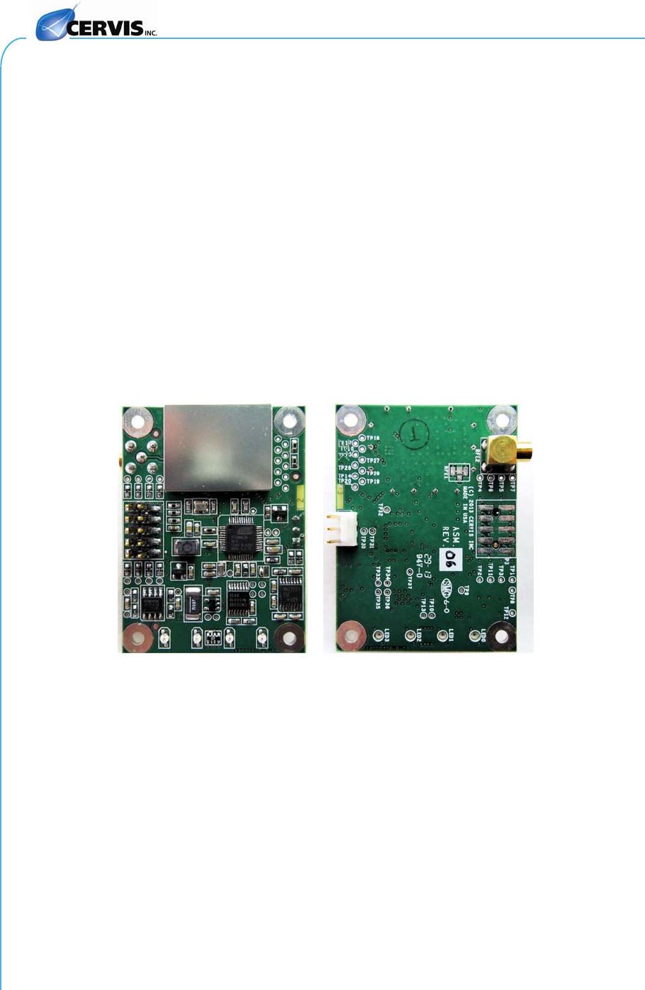
Figure 1. MRF450 Front and Back
User Manual
2014 Cervis, Inc. 3
1.2 Dimensions (mils)/Locations
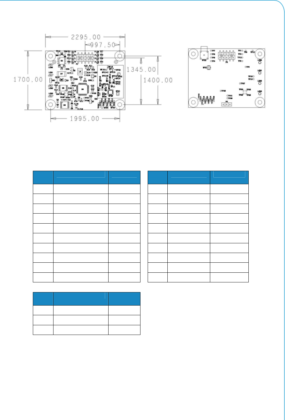
Figure 2. Dimensions (mils)/Locations
1.3 Pinout
Table 1. P1, P2, and P3 Pinout
P1
Pin Assignment I/0 P3
Pin
A
ssignment I/0
P1.1 +VDC 3.3V P1.1 +VDC 3.3V
P1.2 -VDC GND P1.2 TMS IN
P1.3 Enable IN, High P1.3 -VDC GND
P1.4 OC Flag OUT, Low P1.4 TCK IN
P1.5 SPI SCK IN P1.5 -VDC GND
P1.6 SPI SDI / UART RX IN P1.6 TDO OUT
P1.7 SPI SDO / UART TX OUT P1.7 NC NC
P1.8 SPI nSS IN, Low P1.8 TDI IN
P1.9 F0 IN/OUT P1.9 -VDC GND
P1.10 F1 / nRESET IN/OUT P1.10 nRESET IN, Low
P1
Pin Assignment I/0
P1.1 Debug RS232 TX OUT
P1.2 Debug RS232 RX IN
P1.3 REF GND

Module RF450
U077.0.2-MRF450
4
2.0 Installation
When integrating this module into a host, the user must provide all text in the “FCC Statements”
and “Industry Canada Statements” into the host device’s user manual (see Forward Material).
The text must not be modified in any way and presented in a conspicuous manner that the end
user can be reasonably expected to access.
The module is provided with an RF adapter cable and antenna. The RF adapter cable converts
MCX to RP-TNC plug. The connector on the antenna is an RP-TNC jack. Please see section
entitled “FCC Statements” for notice concerning these special accessories.
Install the RF adapter cable by plugging the MCX plug into the MCX jack on the module (RFE2).
Affix the RP-TNC end of the adapter cable to the housing of the host device utilizing the keyed
housing and locking nut. Finally, install the antenna onto the RP-TNC end of the adapter.
3.0 Tune-up Procedure
This module does not require any special tune-up procedure by the user. This module utilizes
advanced system-on-chip (SOC) technology. The SOC is tuned by the foundry at time of
manufacture and is not subject to change or adjustment. The module contains no adjustable
components.
Proper RF operation of the module is verified during the manufacturing process using suitable
equipment and methods. The manufacturer has performed a tuning process according to the
SOC design guidelines.
User Manual
2014 Cervis, Inc. 5
4.0 Electrical Characteristics
4.1 Power
The module requires a regulated 3.3 VDC source. The module does not provide under-voltage,
over-voltage, or reverse polarity protection so use caution when applying power.
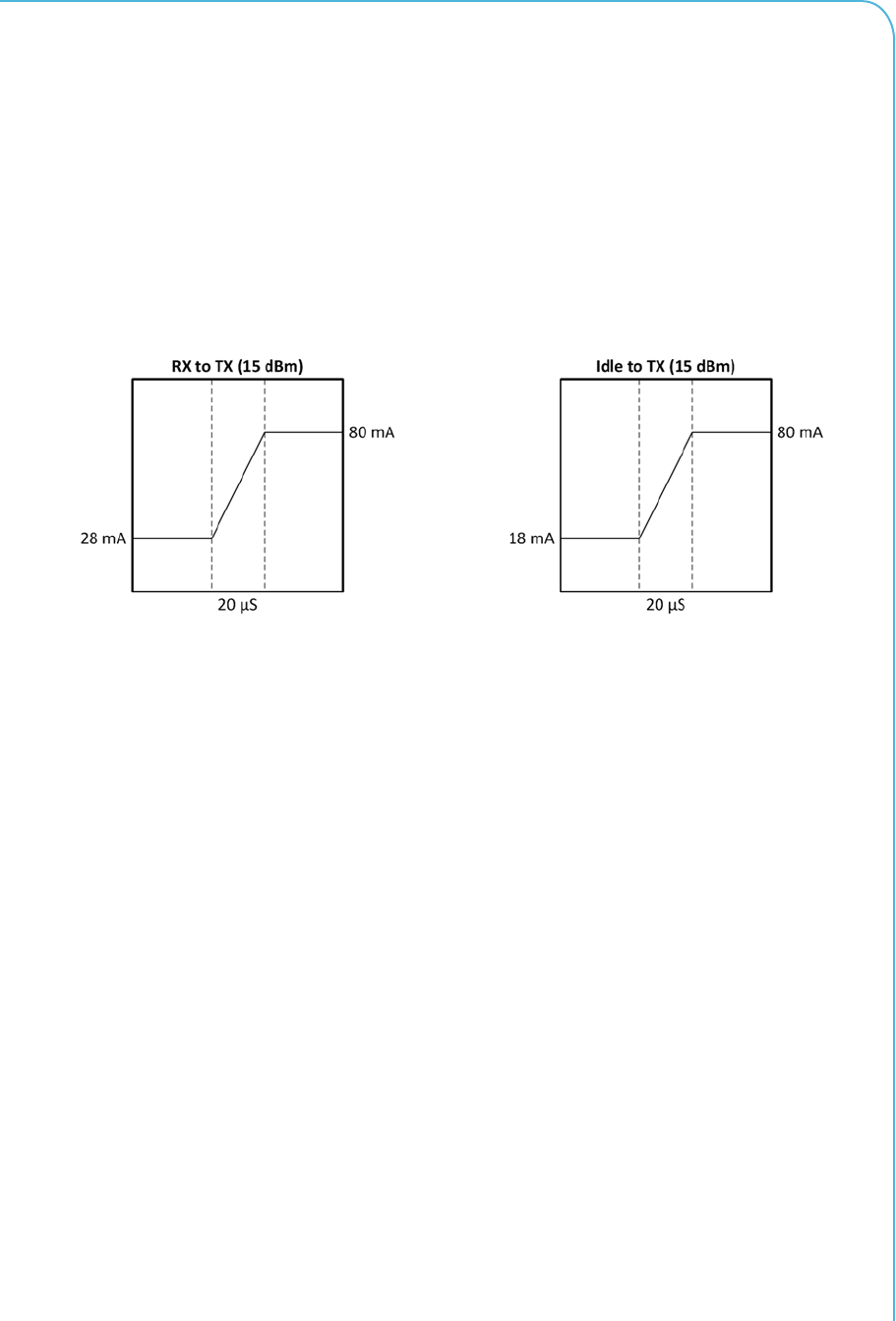
The module transitions between states during normal operation. The integrated PA consumes
the largest amount of power when active. Therefore, transitions to the transmit state will cause
the largest draw on the host supply. It is recommended to provide a large bulk capacitance with
low ESR as close as possible to P1.1 to mitigate host supply drooping during transitions to the
transmit state.
Figure 3 illustrates state transitions vs. current consumption.
Figure 3. State Transitions vs. Current Consumption
4.2 SPI Mode
In SPI mode, P.5 – P1.8 form a SPI slave interface. P1.5 is the input SPI clock generated by the
SPI master (host). The max SCK frequency must be less than 2 MHz. P1.6 is MOSI. P1.7 is
MISO. P1.8 is the input slave select and is active low.
The SPI port is configured for standard SPI Bus Protocol Mode 0. In this mode CPOL (clock
polarity) is 0 meaning that the clock is at a logic low level when idle. CHPA (clock phase) is 1
meaning that data is latched on the rising edge of the clock and changed on the following edge.
The SPI port requires that nSS be asserted at least one bit-time prior to clocking data. nSS may
be released at any time after the last byte has been exchanged. The host must also ensure that
at least one bit-time between consecutive bytes of data is observed.
4.3 UART Mode
In UART mode SCK and nSS (P1.5 and P1.8) are unused and configured as inputs with weak
pull-ups. In this mode UART RX and UART TX (P1.6 and P1.7) provide an asynchronous serial
communications interface. UART RX is configured as an input while UART TX is configured as
an output. The interface is RS-232 compatible with the exception that signaling levels are TTL
logic levels. The port is always configured with 1 start bit, 8 data bits, 1 stop bit, and no parity.
Hardware (RTS and CTS) and software (XON and XOFF) flow control are not utilized. Flow
control is handled by the communications protocol discussed later in this document.
The baud rate of the port can be configured. All standard baud rates from 9600 to 115200 are
supported with less than 4% error. Non-standard baud rates can also be configured, but, not all
requested bauds are possible. Table 2 lists recommended baud rates and associated deviation.
Module RF450
U077.0.2-MRF450
6
Table 2. Recommended Baud Rates and Associated Deviation
Requested
Baud Generated
Baud %
Error
9600 9615 0.16
14400 14493 0.64
19200 19231 0.16
38400 38462 0.16
57600 58824 2.08
115200 111111 3.68
200000 200000 0
250000 250000 0
333333 333333 0
500000 500000 0
1000000 1000000 0
8000000 8000000 0
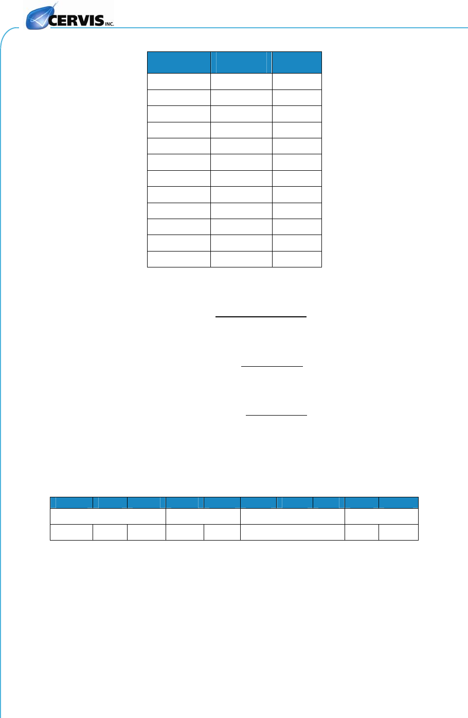
The following formulae are used to calculate the baud rate:
8,000,000
16
Divisor is a 16-bit integer value so be sure to round the result.
8,000,000
16
Finally, calculate the error percentage. Results greater than 4% typically do not work.
1
5.0 RF Characteristics
The OTA structure is formatted as in Table 3.
Table 3. OTA Structure Format
0 .. 4 5 6 7 .. nn + 1 n + 2
Preamble Sync Payload CRC32
0xAA 0xAA 0xAA 0x2D 0xD4 CRC over this region
The module is configured for 12 kbps. This yields 667 µs per byte transmitted. To calculate
time of transmission in seconds, add 10 bytes to the payload count and multiply by 0.000667.
So, a payload of 4 bytes takes (10 + 4) * 0.000667 = 0.009338s, or 9.3 ms on-the-air.
The additional byte (5 Preamble + 2 Sync + 2 CRC32 = 9) comes from the payload structure.
The first byte of the payload is a length indicator used by the module to determine payload
length.

User Manual
2014 Cervis, Inc. 7
6.0 Operational Modes
The module can be configured to operate in one of two modes; Push-To-Transmit mode and
Periodic mode. These modes are discussed in this section. Refer to section “8.1 Get / Set
Parameter” for instructions on changing the operational mode.
6.1 Push-To-Transmit Mode
Push-To-Transmit is the module’s default mode. Any time power is applied to the module it will
begin operation in this mode. This mode is a license-free mode of operation (the operator does
not require a license in order to use the module in this mode, following the requirements set forth
by the FCC in CFR 47 Part 15.231). The module limits the maximum output power to 68.1
dBuV.
In order to comply with license free operation the interaction between the host and module has
restrictions. The host may only issue transmit requests when a manual event occurs on the
host, for example when a button is pressed. There is no limit to the number of transmit requests
that can be issued while the event is active. However, once the event has passed, for example
when the button is released, the host must cease issuing transmit requests within 5 seconds.
Periodic transmit requests are strictly forbidden. This includes, but is not limited to, link
maintenance messages, keep-alive messages, and status messages.
6.2 Periodic Transmit Mode
Periodic Transmit mode is intended for licensed operation (CFR 47 Part 90). The module limits
the maximum output power to +15 dBm. In this mode there are no restrictions between the host
and module, provided the user has configured the module to operate on the frequency channel
for which he holds a license.
It is a violation of CFR 47 to operate this module in Periodic Transmit mode without a license.

Module RF450
U077.0.2-MRF450
8
7.0 Communication Protocol
Communication between the module and host is packetized. Each packet begins with a start-of-
packet (SOP) indicator, followed by the length of the packet message, followed by the message,
and terminated with a checksum calculated over the message. All multi-byte fields are
interpreted in little-endian format; the LSB is stored in the lowest address and the MSB is stored
in the highest. A diagram of the packet format follows.
Table 4. Packet Format Diagram
0 1 2 3.. nn + 1
SOP Message Length Message Chksum
0x3C LSB MSB Chksum Region
The checksum is calculated by subtracting the 8-bit sum of the message bytes from 0xFF. In
this way, the checksum of a packet can be easily verified by summing the message bytes and
checksum. The result of a valid packet is 0xFF.
Handshaking
The synchronization scheme between the module and host varies depending on the
communication channel selected. In either scheme the packet structure remains constant.
7.1 SPI
In SPI mode the module is a slave device. As such, it cannot initiate communications. All
communication is controlled by the host. The module utilizes a buffer for all packets to the host.
F0 (P1.9) is used to communicate the buffer status to the host. When F0 is low, there are no
packets available for the host. When F0 is high, at least one packet is available.
The host must check the state of F0 prior to initiating a SPI transfer. If F0 is low the transaction
will be handled as a write. No data will be shifted out to the host during the transaction. If F0 is
high the transaction will be handled as a read. The module will shift the buffered packet to the
host. Data shifted from the host to the module will be ignored. The polarity of this signal may be
configured (see Pin Mode parameter).
In order to prevent SPI slave overflows, a second control signal is implemented. F1 is utilized as
a CTS (clear to send) signal. The host must check the state of F1 prior to initiating a SPI
transfer. If F1 is asserted the SPI slave interface is busy completing a previously requested
command and any new request will be silently discarded. As soon as nSS is asserted, F1 is
asserted. F1 remains asserted until the requested command completes. The polarity of this
signal may be configured (see Pin Mode parameter).
Due to the structured nature of SPI the likelihood that the module and host lose sync is low. No
additional facilities are provided in this mode.
7.2 UART
In UART mode, both the host and module can initiate communications. In this mode no special
handshaking is required.
In this mode it is potentially possible that the module and host lose sync due to the fact that the
SOP byte can occur as valid data. In order to recover from this condition the protocol also
provides some simple event timeouts. There is no timeout associated with waiting for the SOP
indicator. Once the SOP has been detected an inter-byte timer is started. If the inter-byte
timeout expires an error message is sent to the host and the current packet is discarded. A last-
byte timer is also maintained. This last-byte timer must elapse before an error message is sent.
This ensures that an error message is not sent until the host has completed.

User Manual
2014 Cervis, Inc. 9
The inter-byte timer is set to 10 byte-times. At 115200 baud this is 868 µs. The last-byte timer
is set to 25 byte-times. At 115200 baud this is 2170 µs.
7.3 Acknowledgement
Every packet sent to the module will result in a response packet sent back to the host. In
addition, the module will generate a message to the host when an RF packet is received and
destined for the host. In UART mode the packet will be sent asynchronously. The host must
examine the state of F0 in SPI mode in order to determine if a packet is waiting.
Module RF450
U077.0.2-MRF450
10
8.0 Messages
The heart of the communication packet structure is the message field. This field carries the
specific information of the packet. The first byte of the message field is interpreted as the
message ID. The remaining bytes in the message are interpreted based on the message ID.
The message IDs and structures follow.
Table 5. Message IDs and Structures
0 .. n
ID ID-Dependent
Message Field
8.1 Get / Set Parameter
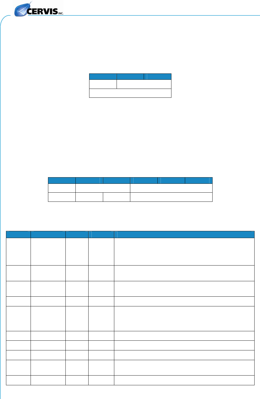
This group of messages is used to set and read module parameters. The first two bytes identify
the specific parameter to be accessed. If data follows the parameter ID, the parameter is set.
The module always replies with the current value of the parameter, or an error code. Each
parameter can vary in data length. See the table of Parameter ID assignment and data lengths
for specific values.
Table 6. Parameter ID Assignment and Data Lengths
Get / Set ID = 0x00, Reply = 0x90.
0 1 2 3 .. n
ID Parameter ID Parameter Value
0x00 Optional. Set if present
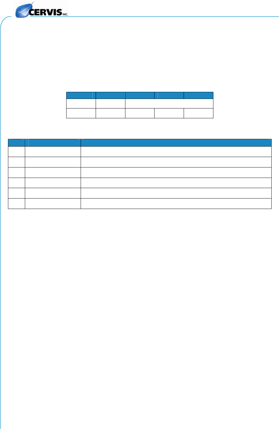
The following table describes the available configurable parameters.
Table 7. Configurable Parameters
ID Parameter Bytes Default Description
0x0000 Channel 2 0x0000 Sets the operating center frequency. 450MHz + (Channel
* 1000). Values above 20,000 are coerced to 20,000.
NOTE: module will NOT transmit until this parameter is
set – even if the desired channel is 0.
0x0001 Power 1 0x00 Sets the output RF power. 0 – 255, logarithmic scale. 255
is no greater than module maximum (see ID 0x0050)
0x0002 LED EN 1 0x0F Bitwise LED enable. A set bit permits LED operation. Bit
0 enables LED0, etc.
0x0003 Baud 4 115200 Sets the baud of the host interface when in UART mode.
0x0004 Pin Mode 1 0x00 Binary-encoded options
1 If clear F0 active low (low when message waiting)
2 If clear F1 active low (high when CTS)
0x0010 My PAN 2 0x0000 Sets the PAN ID of the module.
0x0011 My Address 2 0x0000 Sets the address of the module.
0x0018 DST PAN 2 0x0000 Sets the destination PAN ID for the next transmission.
0x0019 DST
Address 2 0x0001 Sets the destination address for the next transmission.
0xFFFF is a broadcast address.
0x0020 Default 1 0x00 0x00 = Idle. Lower power consumption.

User Manual
2014 Cervis, Inc. 11
ID Parameter Bytes Default Description
Mode 0x01 = RX. Fastest response. ~10 mA more than Idle.
0x0030 RX Filter
Options 1 0x00 Binary-encoded options.
1 If set, filter DST PAN against My PAN
2 If set, filter DST Address against My Address
4 If set, strip DST PAN from payload
5 If set, strip DST Address from payload
6 If set, strip SRC PAN from payload
7 If set, strip SRC Address from payload
If enabled, filter fields must match or the packet is silently
discarded.
Filtering options are processed prior to stripping options.
Enabling filtering on an address field that was not present
in the transmitted packet will result in erroneous packet
discards – filtering will be performed on the specified byte
locations regardless of location contents.
Enabling stripping on an address field that was not present
in the transmitted packet will result in erroneous payloads
– stripping will be performed on the specified byte
locations regardless of location contents.
0x0040 TX Options 1 0x01 Binary-encoded options.
1 If set, perform CCA before transmit
0x0041 CCA
Threshold 1 0x00 NOT YET IMPLEMENTED. CURRENTLY FIXED AT
0x20.
The RSSI value read by the module must be less than this
value before a transmit is performed. If the read RSSI
value is greater or equal, the module will back off a
random length of time (1 – 10 ms) and repeat. See
receive section for RSSI conversion formula.
0x0050 Operational
Mode 1 0x00 0x00 = Push-To-Transmit mode, unlicensed mode
0x01 = Periodic Transmit mode, licensed mode
The mode selected sets the modules maximum RF power
output. Push-To-Transmit mode complies with license-
free operation. Periodic mode is for licensed use only.
Please refer to section “6.0 Operational Modes” for details
and restrictions.
Module RF450
U077.0.2-MRF450
12
8.2 Transmit
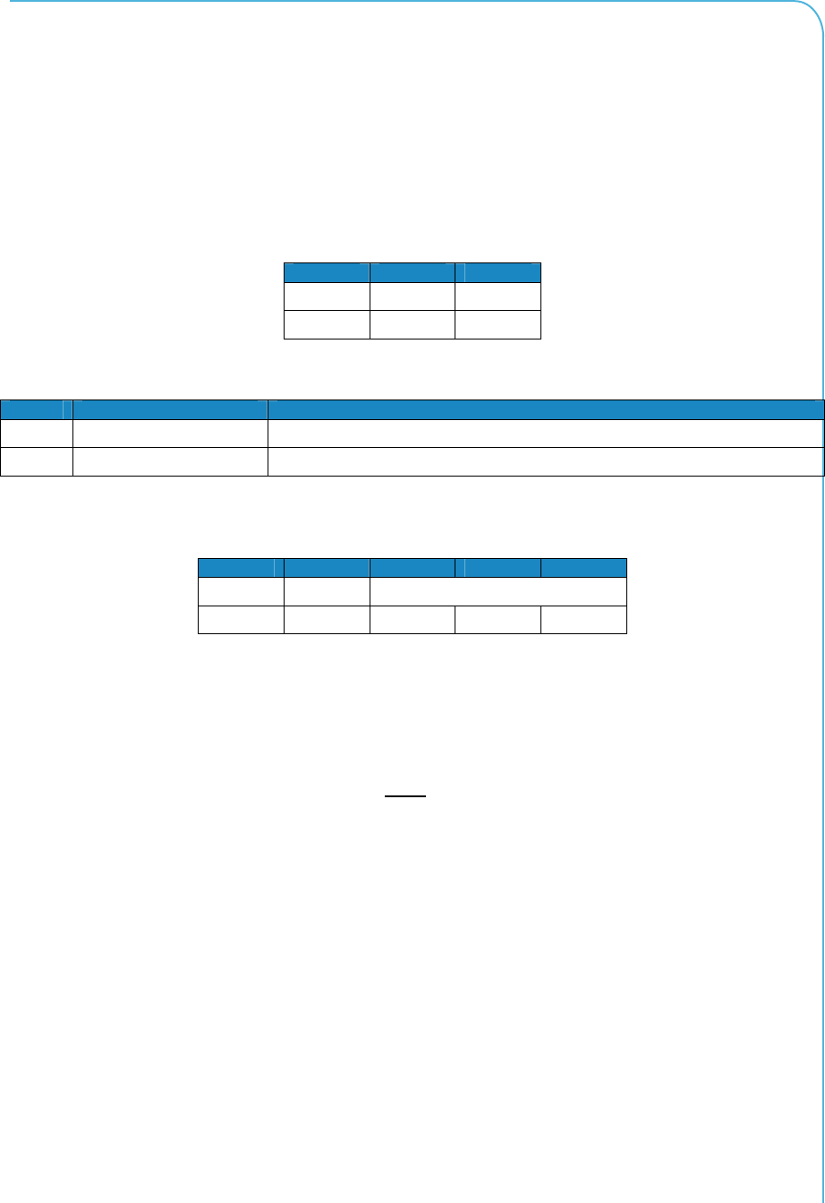
This message instructs the module to transmit a packet. The message contains an options field
followed by the payload to be sent. The maximum payload is 63 bytes. The maximum payload
is further reduced by 2 bytes for each addressing field automatically appended. If all addressing
fields are appended by the module (Options = 0xFX) the maximum payload is 63 – (2 * 4) = 55.
Table 8. Transmit ID, Reply
Transmit ID = 0x10, Reply = 0xA0.
0 1 2.. n
ID Options Payload
0x10
The Options field is binary-encoded and defined as in the following table.
Bit Option Description
0 Message ACK If set, send an ACK message to this transmit request.
1 TX Complete ACK If set, send an ACK message once the packet transmission has completed.
4 DST PAN If set, append the DST PAN parameter to the front of the payload.
5 DST Address If set, append the DST Address parameter to the front of the payload.
6 SRC PAN If set, append the My PAN parameter to the front of the payload.
7 SRC Address If set, append the My Address parameter to the front of the payload.
User Manual
2014 Cervis, Inc. 13
8.3 Receive
This message instructs the module to enter receive mode for the specified time in milliseconds.
The module will dwell in the receive state until a packet is received or the timeout expires. At
this time the module will return to the state specified in the Default Mode parameter. If a
transmit command is issued while this command is active it will clear the receive timer and
terminate the current receive operation. This message is not necessary when the Default Mode
parameter is set to RX.
Table 9. Receive Message Structure
Receive ID = 0x20, Reply = 0xB0.
012
ID Options Time
0x20
The options field is binary-encoded and defined as:
Bit Option Description
0 Message ACK If set, send an ACK message to this receive request.
1 Timeout ACK If set, send an ACK message when the timer expires and no packet was received.
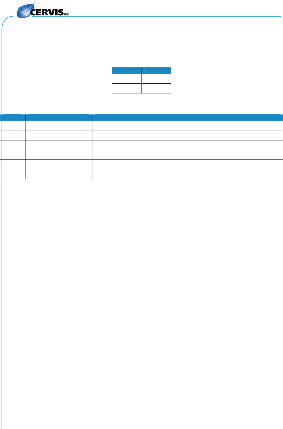
The structure of a received packet varies slightly from the receive request. The structure is
illustrated below.
0 12.. n
ID RSSI Payload
0xB0
The received packet contains the RSSI value as observed during the RF reception of the packet,
along with the packet payload. Based on RX Filter Options, addressing information at the front
of the packet may or may not be present.
The RSSI indicator can be converted to dBm with the following linear formula
2
Offset should be TBD.
Module RF450
U077.0.2-MRF450
14
8.4 Error
This message is sent by the module back to the host to indicate unexpected operation.
Table 10. Error Message Structure
Error ID = 0xFF
0 1
ID Error
0xFF
The Error field is an enumerated type with the following definitions:
Erro
r
Name Description
0 No Error No Error
1 No SOP SOP is missing
2 Length Length of message exceeds maximum
3 CRC CRC mismatch
4 Bad ID Unsupported message ID
5 Bad Parameter Unsupported parameter address

User Manual
2014 Cervis, Inc. 15
Visit our Web site at: www.cervisinc.com
2014 Cervis, Inc. All rights reserved. Content is subject to change without notice.