Cervis SRF305 SRF305 Receive/Transmit Module User Manual
Cervis Inc. SRF305 Receive/Transmit Module Users Manual
Cervis >
Users Manual

2014 Cervis, Inc.
SRF305 User Manual
17 April 2014
U080.0.2-SRF305
™
Module SRF305
This document is the property of Cervis, Inc. and cannot be copied, modified, e-mailed, or reproduced
without the express prior written consent of Cervis, Inc.
Cervis, Inc. reserves the right to change this manual or edit, delete, or modify any information without prior
notification.
Industry Canada Statements
RSS-GEN 7.1.2 – Transmitter Antenna / Antenne de L'émetteur
Under Industry Canada regulations, this radio transmitter may only operate using an antenna of a type and maximum (or lesser) gain approved for the transmitter
by Industry Canada. To reduce potential radio interference to other users, the antenna type and its gain should be so chosen that the equivalent isotropically
radiated power (e.i.r.p.) is not more than that necessary for successful communication.
Conformément à la réglementation d'Industrie Canada, le présent émetteur radio peut fonctionner avec une antenne d'un type et d'un gain maximal (ou inférieur)
approuvé pour l'émetteur par Industrie Canada. Dans le but de réduire les risques de brouillage radioélectrique à l'intention des autres utilisateurs, il faut choisir le
type d'antenne et son gain de sorte que la puissance isotrope rayonnée équivalente (p.i.r.e.) ne dépasse pas l'intensité nécessaire à l'établissement d'une
communication satisfaisante.
This radio transmitter 7955A-SRF305 has been approved by Industry Canada to operate with the antenna types listed below with the maximum permissible gain
and required antenna impedance for each antenna type indicated. Antenna types not included in this list, having a gain greater than the maximum gain indicated
for that type, are strictly prohibited for use with this device.
Le présent émetteur radio 7955A-SRF305 a été approuvé par Industrie Canada pour fonctionner avec les types d'antenne énumérés ci-dessous et ayant un gain
admissible maximal et l'impédance requise pour chaque type d'antenne. Les types d'antenne non inclus dans cette liste, ou dont le gain est supérieur au gain
maximal indiqué, sont strictement interdits pour l'exploitation de l'émetteur.
Approved Antenna List / Liste Antenne Approuvé
Manufacturer Part Number Stock Number Gain Impedance
Antenna-Factor/Linx Tech ANT-2.4-uSP B141 +3.8dBipeak 50 Ohm
RFM
Or Equivalent
OMNI242R
Or Equivalent
BB3-07 +3dBipeak 50 Ohm
Alfa
Or Equivalent
ARSN19TNC
Or equivalent
BB3-08 +9dBipeak 50 Ohm
RSS-GEN 7.1.3 – Notice / Délai
This device complies with Industry Canada licence-exempt RSS standard(s). Operation is subject to the following two conditions: (1) this device may not cause
interference, and (2) this device must accept any interference, including interference that may cause undesired operation of the device.
Le présent appareil est conforme aux CNR d'Industrie Canada applicables aux appareils radio exempts de licence. L'exploitation est autorisée aux deux
conditions suivantes : (1) l'appareil ne doit pas produire de brouillage, et (2) l'utilisateur de l'appareil doit accepter tout brouillage radioélectrique subi, même si le
brouillage est susceptible d'en compromettre le fonctionnement.
FCC Statements
15.19 – Two Part Warning
This device complies with Part 15 of the FCC rules. Operation is subject to the following two conditions:
(1) This device may not cause harmful interference and
(2) This device must accept any interference received, including interference that may cause undesired operation.
15.21 – Unauthorized Modification
NOTICE: The manufacturer is not responsible for any unauthorized modifications to this equipment made by the user. Such modifications could void the user’s
authority to operate the equipment.
15.27 – Special Accessories
This device is supplied with special accessories that include an RF adapter cable and antenna. These special accessories must be used with the device. It is the
responsibility of the user to use the needed special accessories supplied with the equipment.
15.105(b) – Note:
This equipment has been tested and found to comply with the limits for a Class A digital device, pursuant to part 15 of the FCC Rules. These limits are designed
to provide reasonable protection against harmful interference when the equipment is operated in a commercial environment. This equipment generates, uses,
and can radiate radio frequency energy and, if not installed and used in accordance with the instruction manual, may cause harmful interference to radio
communications. Operation of this equipment in a residential area is likely to cause harmful interference in which case the user will be required to correct the
interference at his own expense.

User Manual
2014Cervis, Inc. i
Table of Contents
Table of Contents .......................................................................................................................... i
List of Figures ............................................................................................................................... i
List of Tables ................................................................................................................................. i
Cervis Inc. Safety Precautions ................................................................................................... 1
1.0SRF305 Introduction ............................................................................................................ 2
1.1SRF305 Features ............................................................................................................... 2
1.2SRF305 Pinouts ................................................................................................................ 4
2.0SRF305 Installation ............................................................................................................ 14
3.0SRF305 Tune-up Procedure .............................................................................................. 14
4.0SRF305 Electrical Characteristics .................................................................................... 14
4.1Supply Voltage and Current .......................................................................................... 14
4.2Operating Current ........................................................................................................... 15
4.3SPI Interface .................................................................................................................... 15
5.0SRF305 RF Characteristics ............................................................................................... 15
List of Figures
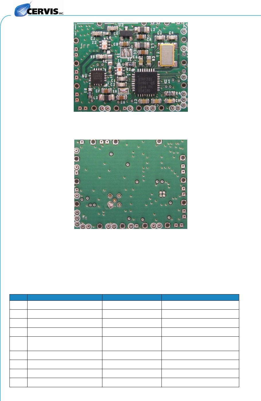
Figure 1. SRF305 RF section Front .............................................................................................. 4
Figure 2. SRF305 RF section Back ............................................................................................... 4
Figure 3. 07440305-2H-12R, component side, shield removed ................................................. 6
Figure 4. 07420305-2H-12R, component side .............................................................................. 8
Figure 5. 07610304-2H, component side .................................................................................... 10
Figure 6. 07610304-2H, bottom side ........................................................................................... 10
Figure TBD. 07100366-2H, component side .............................................................................. 13
List of Tables
Table 1. 07440205 PCB – connector HDR1 .................................................................................. 4
Table 2. 07420205 PCB – connector HDR1 .................................................................................. 7
Table 3. 07610204 PCB – connector J1 ........................................................................................ 9
Table 4. 07100266 PCB – connector J1 (preliminary) ............................................................... 12

Module SRF305
U080.0.2-SRF305 User Manual
ii
Notes and Observations

User Manual
Cervis Inc. Safety Precautions
Read and follow all instructions.
Failure to abide by Safety Precautions may result in equipment failure, loss of
authority to operate the equipment, and personal injury.
Use and maintain proper wiring. Follow equipment manufacturer instructions.
Improper, loose, and frayed wiring can cause system failure, equipment damage, and
intermittent operation.
Changes or modifications made to equipment not expressly approved by the
manufacturer will void the warranty.
Owner/operators of the equipment must abide by all applicable Federal, State, and
Local laws concerning installation and operation of the equipment. Failure to comply
could result in penalties and could void user authority to operate the equipment.
Make sure that the machinery and surrounding area is clear before operating. Do not
activate a remote control system until certain that it is safe to do so.
Turn off the module power before attempting any maintenance. This will prevent
accidental operation of the controlled machinery.
Do not allow liquid to enter the module enclosure. Do not use high pressure
equipment to clean the module.
Operate and store units only within the specified operation and storage temperatures
defined in the Specifications of this document.

Module SRF305
U080.0.2-SRF305 User Manual
2
1.0 SRF305 Introduction
The SRF305 receive/transmit module (RTM) is based on a single-chip radio frequency (RF)
transceiver integrated circuit (RFIC), an Atmel AT86RF231. The RT module also contains an
external RF transmit power amplifier plus low noise RF receive preamplifier integrated circuit
(PA/LNA), an RFaxis RFX2401C. The SRF305 RTM is intended to be integrated into Cervis Inc.
products, providing a wireless RF connectivity option.
The SRF305 RTM operates in the 2.45 GHz ISM band, using spread spectrum modulation
with a maximum conducted RF transmit power of +19.95dBm at the antenna port.
The RFIC generates RF signals compliant with the Zigbee standard, IEEE 802.15.4-2006.
The spread spectrum technique is direct sequence (DSSS), the modulation method is
orthogonal quadrature phase shift keying (O-QPSK).
The RFIC has internal control registers that the host application can access via a serial
peripheral (SPI) bus. These registers control all aspects of how the RFIC is used, which must be
compliant with all applicable rules and regulations.
The SR305 RTM is interoperable various other Cervis Inc. RTMs that use the same
modulation and message data structure. Interoperability with non-Cervis RTMs, while possible,
is not supported.
The SRF305 RTM is most commonly applied in half-duplex master/slave systems: the master
transmits a message to a slave, the slave transmits a reply to the master. Other operating
modes are possible, provided that applicable rules and regulations are not violated.
The SRF305 RTM may be realized in various PCB shapes, some with non-RF circuits
applicable to the requirements of particular hot applications. Variations include:
07440305-2H-12R “large mezzanine” (tested, pictured)
07610304-2H “mini-module” (tested, pictured)
07420305-2H-12R “small mezzanine” (not yet tested)
07100366-2H “postage stamp” (not yet tested)
1.1 SRF305 Features
FCC Part 15 certified
IC Certified
CE certified
2405-2480 MHz Operation
5 MHz Selectable Channel
Orthogonal Quadrature Phase Shift Keying (O-QPSK)
Direst Sequence Spread Spectrum (DSSS)
250 kbps Data Rate (tested)
500 kbps Data Rate (capable, not tested)
1000 kbps Data Rate (capable, not tested)
2000 kbps Data Rate (capable, not tested)
Up to +19.95dBm Output Power (tested)
Use with a variety of approved, supplied internal and external antennas
IEEE 802.15.4-2006 messaging
SPI host interface
Simple power requirements
Compliant will all FCC (and equivalent IC) requirements for a modular transmitter:
In accordance with FCC Rule Part 15.212 for the product certified under FCC ID:

User Manual
2014Cervis, Inc. 3
LOBSRF305, the following elements confirm that LOBSRF305 complies with the
definition of a modular transmitter:
a. The radio elements of the modular transmitter have their own shielding. The physical
crystal and tuning capacitors are located internal to the shielded radio elements.
b. The modular transmitter has buffered modulation/data inputs to ensure that the
module will comply with part 15 requirements under conditions of excessive data
rates or over-modulation.
c. The modular transmitter has its own power supply regulation.
d. The modular transmitter complies with the antenna and transmission system
requirements of §§15.203, 15.204(b) and 15.204(c). hen installed in the host
application, the antenna is either be permanently attached or employs a “unique”
antenna coupler (at all connections between the module and the antenna, including
the cable). The “professional installation” provision of §15.203 is not applicable to
modules but can apply to limited modular approvals under paragraph (b) of this
section.
e. The modular transmitter has been tested in a stand-alone configuration, i.e., the
module must not be inside another device during testing for compliance with part 15
requirements. When the transmitter module is not battery powered it complies with
the AC line conducted requirements found in §15.207. AC or DC power lines and
data input/output lines connected to the module do not contain ferrites, unless they
will be marketed with the module (see §15.27(a)). The length of these lines shall be
the length typical of actual use or, if that length is unknown, at least 10 centimeters to
insure that there is no coupling between the case of the module and supporting
equipment. Any accessories, peripherals, or support equipment connected to the
module during testing shall be unmodified and commercially available (see
§15.31(i)).
f. The modular transmitter is equipped with a permanently affixed label displaying its
FCC identification number.
g. The modular transmitter complies with any specific rules or operating requirements
that ordinarily apply to a complete transmitter and the manufacturer must provide
adequate instructions along with the module to explain any such requirements. A
copy of these instructions must be included in the application for equipment
authorization.
h. The modular transmitter must comply with any applicable RF exposure requirements
in its final configuration.
Module SRF305
U080.0.2-SRF305 User Manual
4
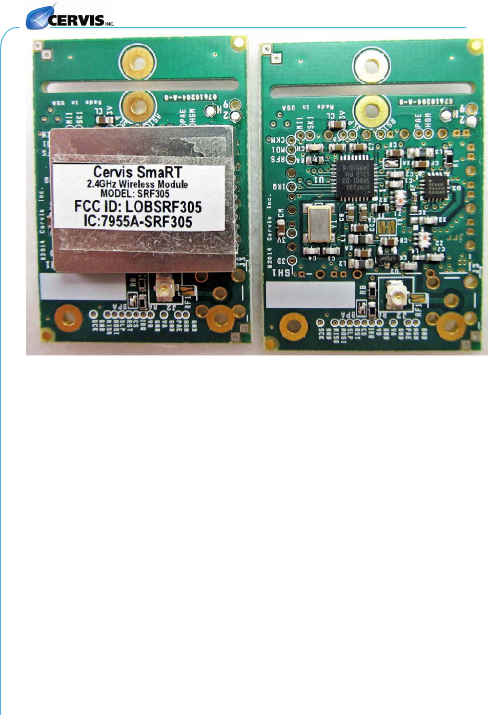
Figure 1. SRF305 RF section Front
Figure 2. SRF305 RF section Back
1.2 SRF305 Pinouts
Table 1-4 show the pinouts and interface signals on several alternative packaging options for the
SRF305 RTM:
Table 1. 07440205 PCB – plug-in connector HDR1
Pin Name Signal Details
1 SPI_CLK SPI data clock in Clock from SPI master
2 GND ground Low impedance ground
3 MISO SPI data out Data from SPI slave
4 MOSI SPI data in Data from SPI master
5 RF_SLP_TR RFIC control Multipurpose control signal from
master
6 /RF_RST RFIC reset Low from SPI master
7 /RF_CS RFIC chip select Low from SPI master
8 RF_IRQ RFIC interrupt output Input to SPI master
9 RF_PAEN Enable external PA High from SPI master

User Manual
2014Cervis, Inc. 5
10 RF_HGM/BPA Enable external LNA or
Read BPA jumper
Function not used in SRF305
Input to SPI master
11 GND ground Low impedance ground
12 GND ground Low impedance ground
13* DISPLAYCS Display chip select Low from SPI master
14* /RFEE_CS (reserved) EE chip select Low from SPI master
15* DISPLAYRS Display register select From SPI master
16* DISPLAYBLANK Display on/off From SPI master
17 reserved reserved reserved
18 reserved reserved reserved
19* DISPLAYRST Display reset Low from SPI master
20 reserved reserved reserved
21* LED_6 Indicator High from SPI master
22* LED_7 Indicator High from SPI master
23* LED_4 Indicator High from SPI master
24* LED_5 Indicator High from SPI master
25* LED_2 Indicator High from SPI master
26* LED_3 Indicator High from SPI master
27* LED_0 Indicator High from SPI master
28* LED_1 Indicator High from SPI master
29 GND ground Low impedance ground
30 GND ground Low impedance ground
31* +24VDC +3.0-30V Power indicator LED
32* +5VDC +3.0-30V Power indicator LED
33 +3.3VDC +3.3V Power indicator LED, RF & logic
power. Low noise 150mA max.
34* REVBAT +3.0-30V Power indicator LED
*Not required for SRF305
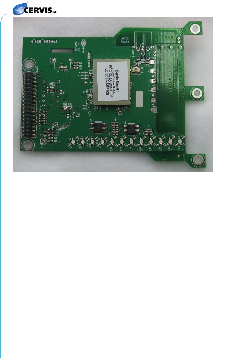
The 07440305-2H-12R PCB assembly includes all circuits and features required for properly
implementing the SRF305 RTM. The PCB also provides circuits and mounting for various
optional non-RF features of use to a host application, including:
12 indicator LEDs (default installation)
LED/LCD display module (future use)
Module SRF305
U080.0.2-SRF305 User Manual
6
Figure 3. 07440305-2H-U-12R, component side, shield, internal label, external antenna
connector
User Manual
2014Cervis, Inc. 7
Table 2. 07420205 PCB – plug-in connector HDR1
Pin Name Signal Details
1* /RFEE_CS (reserved) EE chip select Low from SPI master
2 RF_SLP_TR RFIC control Multipurpose control signal from
master
3 /RF_RST RFIC reset Low from SPI master
4 RF_IRQ RFIC interrupt output Input to SPI master
5 /RF_CS RFIC chip select Low from SPI master
6 RF_PAEN Enable external PA High from SPI master
7 RF_HGM/BPA Enable external LNA or
Read BPA jumper
Function not used in SRF305
Input to SPI master
8 SPI_CLK SPI data clock in Clock from SPI master
9 MOSI SPI data in Data from SPI master
10 MISO SPI data out Data from SPI slave
11 GND ground Low impedance ground
12 GND ground Low impedance ground
13* LED_7 Indicator High from SPI master
14* LED_6 Indicator High from SPI master
15* LED_5 Indicator High from SPI master
16* LED_4 Indicator High from SPI master
17* LED_3 Indicator High from SPI master
18* LED_2 Indicator High from SPI master
19* LED_1 Indicator High from SPI master
20* LED_0 Indicator High from SPI master
21 GND ground Low impedance ground
22 GND ground Low impedance ground
23* REVBAT +3.0-30V Power indicator LED
24* +5VDC +3.0-30V Power indicator LED
25 +3.3VDC +3.3V Power indicator LED, RF & logic
power. Low noise 150mA max.
26* +24VDC +3.0-30V Power indicator LED
*Not required for SRF305
The 07420305-2H-x-12R PCB assembly is similar to the approved 07440305-2H-x-12R PCB
assembly, except for a change in the shape and connector to accommodate use in host
applications that utilize the form-factor of the 07420305-2H-x-12R. Except for some minor
differences outside the shielded RF section, the operation of 07420305-2H-x-12R is compliant
with the SRF305 modular approval, as demonstrated by testing.
The 07420305-2H-x-12R PCB assembly includes all circuits and features required for
properly implementing the SRF305 RTM. The PCB also provides circuits and mounting for
various optional non-RF features of use to a host application, including:
12 indicator LEDs (default installation)

Module SRF305
U080.0.2-SRF305 User Manual
8
Insert image of 074200305-2H-12R when available
Figure 4. 07420305-2H-U-12R, component side, shield, internal label, external antenna
connector

User Manual
2014Cervis, Inc. 9
Table 3. 07610204 PCB – plug-in connector J1
Pin Name Signal Details
1 SPI_CLK SPI data clock in Clock from SPI master
2 GND ground Low impedance ground
3 MISO SPI data out Data from SPI slave
4 MOSI SPI data in Data from SPI master
5 RF_SLP_TR RFIC control Multipurpose control signal from
master
6 /RF_RST RFIC reset Low from SPI master
7 /RF_CS RFIC chip select Low from SPI master
8 RF_IRQ RFIC interrupt output Input to SPI master
9 RF1_3VD +3.0-3.3V RF & logic power. Low noise
125mA max.
10 GND ground Low impedance ground
11 RF1_3VA +3.0-3.3V RF analog power. Low noise
25mA max.
12 GND ground Low impedance ground
13 RF_PAEN Enable external PA High from SPI master
14 RF_HGM/BPA Enable external LNA or
Read BPA jumper
Function not used in SRF305
Input to SPI master
15 GND ground Low impedance ground
The 07610304-2H-x PCB assembly is similar to the approved 07440305-2H-x-12R PCB
assembly, except for elimination of non-RF circuits and a change in the shape and connector to
accommodate use in host applications that utilize the form-factor of the 07610304-2H-x. Except
for some minor differences outside the shielded RF section, the operation of 07610304-2H-x is
compliant with the SRF305 modular approval, as demonstrated by testing.
The RF connection of 076100304-2H-x is always via a coaxial cable and unique connector.
The 07610304-2H-x PCB assembly includes all circuits and features required for properly
implementing the SRF305 RTM
Module SRF305
U080.0.2-SRF305 User Manual
10
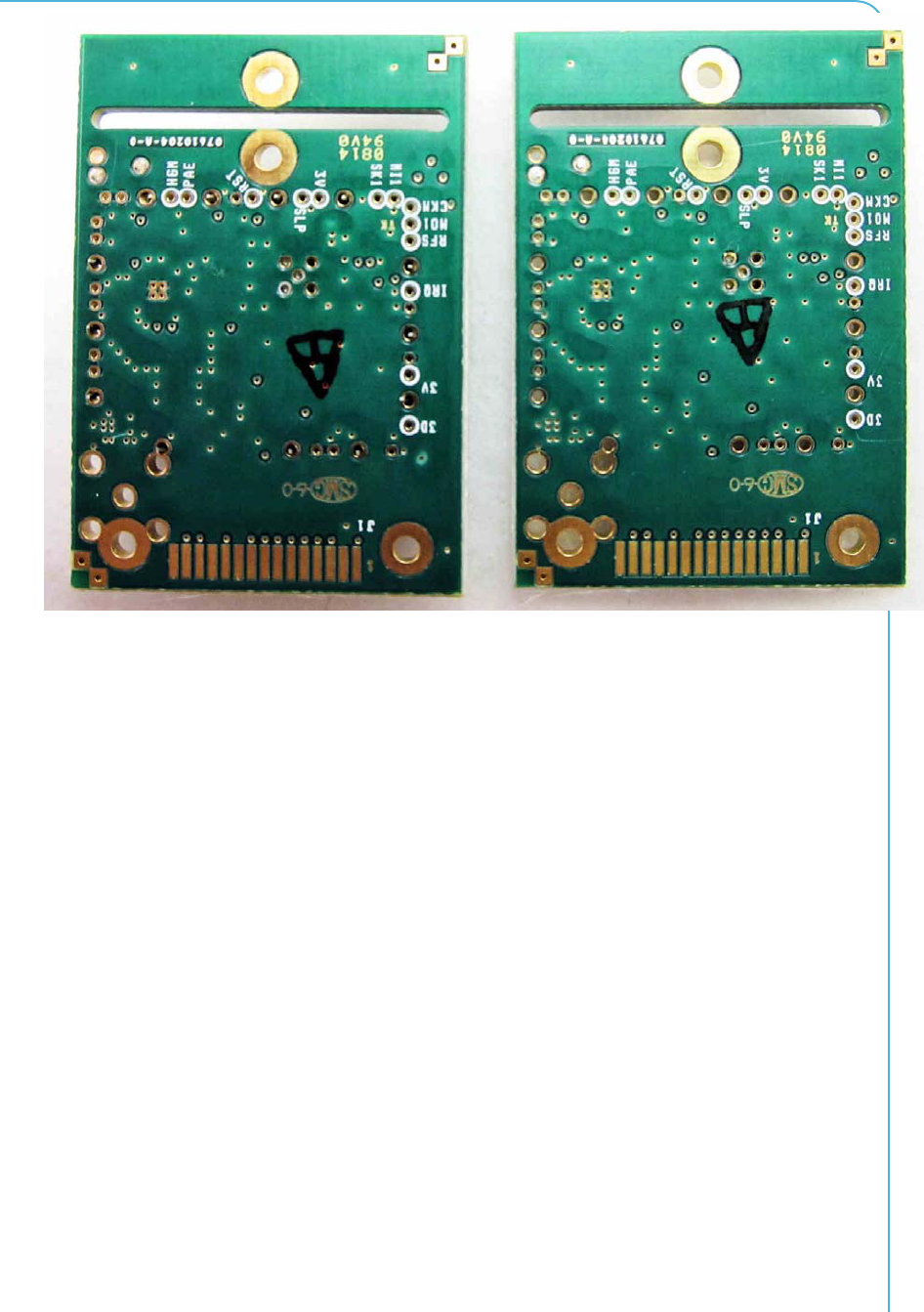
Figure 5. 07610304-2H-U, component side, shield, internal label, external antenna connector
User Manual
2014Cervis, Inc. 11
Figure 6. 07610304-2H-U, bottom side.
Module SRF305
U080.0.2-SRF305 User Manual
12
Table 4. 07100266 PCB – solder-down connector J1 (preliminary)
Pin Name Signal Details
1 SPI_CLK SPI data clock in Clock from SPI master
2 GND ground Low impedance ground
3 MISO SPI data out Data from SPI slave
4 MOSI SPI data in Data from SPI master
5 RF_SLP_TR RFIC control Multipurpose control signal from
master
6 /RF_RST RFIC reset Low from SPI master
7 /RF_CS RFIC chip select Low from SPI master
8 RF_IRQ RFIC interrupt output Input to SPI master
9 RF1_3VD +3.3V RF & logic power. Low noise
150mA max.
10 GND ground Low impedance ground
11 RF1_3VA +3.3V RF analog power. Low noise
15mA max.
12 GND ground Low impedance ground
13 RF_PAEN Enable external PA High from SPI master
14 RF_HGM/BPA Enable external LNA or
Read BPA jumper
Function not used in SRF305
Input to SPI master
15 GND ground Low impedance ground
16 RF RF signal, in/out 50-Ohm RF connection to antenna
17 GND ground Low impedance ground
18 GND ground Low impedance ground
19 GND ground Low impedance ground
20 GND ground Low impedance ground
The 07100366-2H PCB assembly is similar to the approved 07440305-2H-x-12R PCB
assembly, except for elimination of non-RF circuits and a change in the shape and connector to
accommodate use in host applications that utilize the form-factor of the 07100366-2H. Except for
some minor differences outside the shielded RF section, the operation of 07610366-2H is
compliant with the SRF305 modular approval, as demonstrated by testing.
The RF connection of 07100366-2H-x is always via a soldered connection to a suitable 50
Ohm RF transmission line.
The 07100366-2H PCB assembly is factory-installed by direct soldering to a matching
footprint on a PCB that is part of the host application. The host application PCB must also
provide a suitable RF connection to either a fixed internal antenna or a coaxial cable connection
to a unique connector for attaching an approved, supplied external antenna.
The 07100366-2H PCB assembly includes all circuits and features required for properly
implementing the SRF305 RTM.
Insert image of 07100366-2H when available

User Manual
2014Cervis, Inc. 13
Figure 6. 07100366-2H, component side, shield, internal label

Module SRF305
U080.0.2-SRF305 User Manual
14
2.0 SRF305 Installation
When integrating an SRF305 RTM into a host application, the user must provide all text in the
“FCC Statements” and “Industry Canada Statements” in the host application’s user manual (see
Forward Material). The text must not be modified in any way and presented in a conspicuous
manner that the end user can be reasonably expected to access.
When integrating the SRF305 RTM into host application hardware, the user must properly
connect all the circuits identified in Table 1 to suitable host application signals. The host
application firmware must properly control the RTM to ensure that emitted RF signals comply
with all applicable regulatory approvals.
The SRF305 RTM is always provided with an approved type of antenna, either internal fixed
or external replaceable. If a fixed internal antenna is provided as part of the RTM, the on-board
coaxial cable connectors are not populated. If the module is assembled for use with an external
antenna, one of the on-board coaxial cable connector positions will be populated. The choice of
the particular type of coaxial connector that is installed will be decided by the designer of the
host application. The on-board connector is not accessible to users, so it does not need to be
unique.
When provided, external replaceable antennas always have a unique connector such as: RP-
N, U.FL/IPEX, RP-SMA, RP-BNC or RP-TNC. A suitable coaxial cable jumper with appropriate
connectors must be used to connect the SRF305 RTM external antenna port to the external
antenna. The details of a particular host application will affect the design of the jumper coax, but
the external connector must always be of an acceptable unique type.
The coaxial cable used to make the jumper between the RTM and the external antenna
mounting position must be suitable for use at 2450 MHz and have 50 Ohm impedance. Low loss
cable such as RG-316 is suggested, although signal loss will be small if the jumper length is
short.
External coaxial cables may be used to help mount the replaceable external antenna in a
more useful location. Such cable must have appropriate unique connectors and must be made
from low loss 50 Ohm coaxial cable. Cables equivalent to LMR-195 are suitable for lengths up to
30 feet. Longer cables must have suitably lower signal loss, typically using larger cable such as
LMR240, LMR-300, or larger (or equivalent). At some point, a practical limit is reached where
losses in extension cables negate any gains from relocating the antenna.
3.0 SRF305 Tune-up Procedure
There is no tune-up procedure. The module contains no adjustable components.
Proper RF operation of the module is verified during the manufacturing process using
suitable equipment and methods.
4.0 SRF305 Electrical Characteristics
4.1 Supply Voltage and Current
The SRF305 RTM by itself requires a low noise regulated 3.0-3.3 VDC source that can
provide 150mA without losing regulation. The module does not provide under-voltage, over-
voltage, or reverse polarity protection so use caution when applying power. It is the responsibility
of the host application to provide an appropriate source of 3.0-3.3V adequate to power the RTM,
plus any other non-RF circuits that may also be implemented on the same PCB.
All external connection points designate as signal “GND” should be connected to the host
application “GND” circuit so as to maintain a low resistive and reactive impedance as practical.

User Manual
2014Cervis, Inc. 15
The PCB hosting the RTM should be fabricated with low impedance copper floods that connect
to “GND”.
The SRF305 RTM can safely operate with a supply voltage over the range of 3.0-3.3V with
minimal changes in RF performance.
4.2 Operating Current
The SRF305 RTM has four primary operating conditions that draw differing amounts of current
from to 3.0-3.3V power source:
Off RFIC is powered down, minimal load
PLL_ON RFIC is ready to transmit or receive, ~5mA
RX RFIC is receiving a message, ~12mA
TX RFIC is transmitting, ~15-100mA, depending on TX output power
In TX mode the operating current may be less than the maximum if the drive to the external
PA is reduced because the full +19.95dBm RF output power is not required.
4.3 SPI Interface
The SPI interface between the RFIC (slave) and the host application (master) microcontroller
requires four signals:
SCLK – The serial data clock from the SPI master. Muste be less than 8 MHz.
MOSI – Serial data from the SPI master.
MISO – Serial data from the SPI slave.
RF_CS – Chip select from the SPI master.
The SPI controller setting must be established by the host application microcontroller to be
compatible with the SPI interface timing specified by the RFIC data sheet.
5.0 SRF305 RF Characteristics
The RFIC used in the SRF305 RTM implements RF modulation modes and timings in
compliance with IEEE 802.15.4-2006. The RFIC implements additional proprietary RF
modulation modes. Details may be found in the At86RF231 RFIC data sheet.
The SRF305 supports four data bitrates: 250, 500, 1000 and 2000 kbps. The general spread
spectrum scheme is the same for all, O-QPSK and DSSS. There are differences in the
spreading methods that result in slightly different spectral distributions within the nominal 5MHz
channel width. Conducted and radiated emissions testing will need to be performed for all data
bitrates that are to be approved.

Module SRF305
U080.0.2-SRF305 User Manual
16
Visit our Web site at: www.cervisinc.com
2014 Cervis, Inc. All rights reserved. Content is subject to change without notice.