Cheng Uei Precision Industry MV84PG EVDO PCIe DATA CARD User Manual MV84PG User Guide Rev6
Cheng Uei Precision Industry Co., Ltd. EVDO PCIe DATA CARD MV84PG User Guide Rev6
Users Manual

1
Document Title MV84PG Installation Manual
Version V1.4
Date 2011/8/31
Copyright
FOXLINK is a registered trademark of FOXLINK Incorporated.
Copyright © 2011 FOXLINK Incorporated. All rights reserved.
No part of this publication may be reproduced or distributed in any form or by any means, or
stored in a database or retrieval system, without the prior written permission of the publisher.
FOXLINK Incorporated reserves the right to make changes in technical and product
specifications without provisional notification.
This module is limited to OEM installation only and must not be sold to end-users.
OEM integrators must be instructed to ensure that the end-user has no manual instructions to
Remove or install the device.
The end-user can not remove or install this module to any other devices.
2
Contents
1 MV84PG introduction ...........................................................................................................................................3
1.1 Two side view.............................................................................................................................................3
1.2 PCIe card introduction................................................................................................................................4
1.3 MV84PG accessory....................................................................................................................................5
2 Operational description ........................................................................................................................................6
2.1 Test Board Manual .....................................................................................................................................6
2.1.1 Preparation before operation............................................................................................................6
2.2.2 Test board description ......................................................................................................................7
2.2.3 Test steps .........................................................................................................................................8
2.3 Operational description ..............................................................................................................................8
2.3.1 Tune up procedure ...........................................................................................................................8
3 MV84PG features.................................................................................................................................................9
3.1 General specification..................................................................................................................................9
3.2 Hardware Specification ............................................................................................................................10
4. Standards and Regulatory Compliance ............................................................................................................. 11
4.1 Standards and certification....................................................................................................................... 11
4.2 FCC certification requirements.................................................................................................................12
4.3 FCC RF exposure requirements ..............................................................................................................13
3
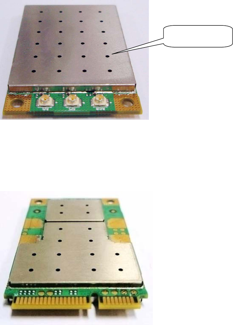
1 MV84PG introduction
1.1 Two side view
Device
View 1:
Device
View 2:
FCC Label is on this
cover
4
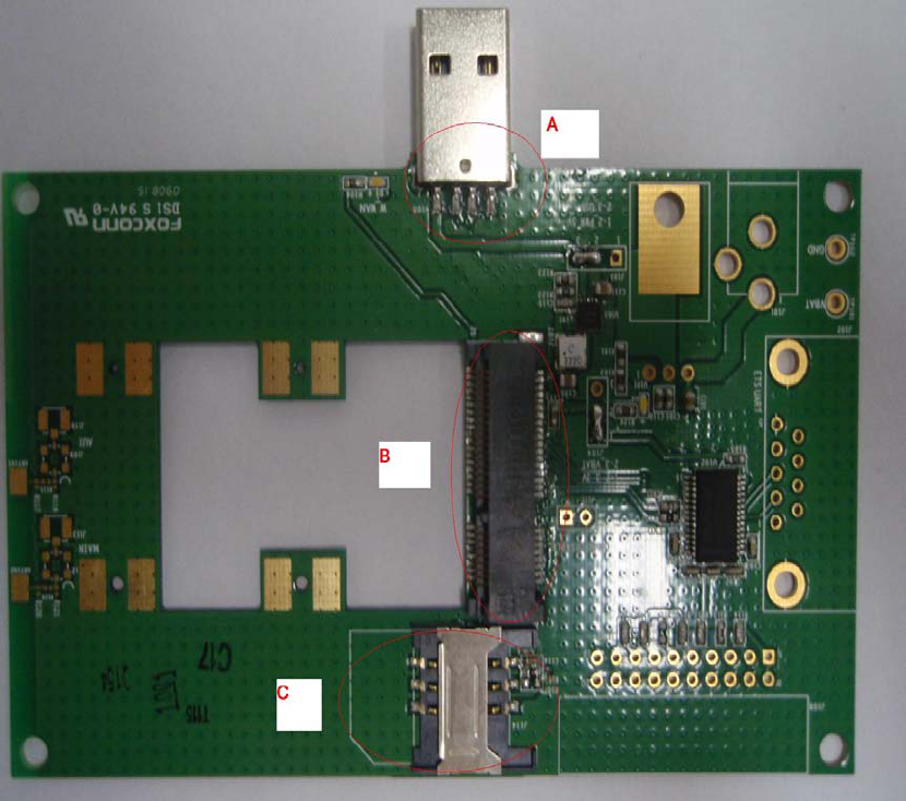
1.2 PCIe card introduction
Devise test equipment tool
View 3:
A: USB port
B: MV84PG card socket
C: SIM card socket
5
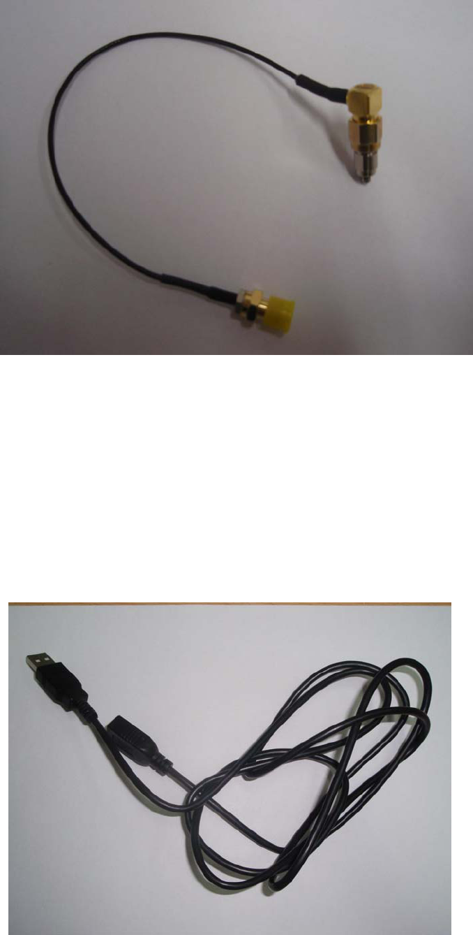
1.3 MV84PG accessory
RF cable
View 7:
USB to UART converter cable
View 8:
6
2 Operational description
2.1 Test Board Manual
2.1.1 Preparation before operation
MV8X test board provides an environment to test and estimate the CDMA module of
MV8X series, meanwhile, proposes a reference for hardware design.
MV8X test board provides all the 52PIN interface to the external, and users could finish
their development and application through the test board without separately making board.
With this MV8X test board, you could carry on these tests and estimates of function about
MV8X series as below:
1.1 Connection to Serial Interface and AT Order Set
1.2 Wireless Data MODEM
Before operation,please read relative documents(MV8X AT Order Manual), and
confirm that relative accessories and devices as below are ready:
1.3 One MV8X Series Module.
1.4 Two or Three Both End U.FL(IPEX) RF Connecting Wires
1.5 800MHz、1900MHz GPS antenna for each
1.6 One DB9 Femal Wire(Self-prepare)
1.7 One USB Extension Wire
1.8 One Test Board Power Wire DC_JACK_2p2 Interface Wire(Self-prepare)
1.9 Adjustable or Fixed DC Regulated Power Supply(Self-prepare)
7
2.2.2 Test board description
Please acquaint yourself with interfaces according to the test board:
2.1 J105:USB interface, module and PC data com port
2.2 TP101:+3.3V
2.3 TP102:GND
2.4 J101:DC_JACK_2p2 power supply interface
2.5 J103,J104:Power supply option:
a. If J103 move to 1、2, J104 move to 1、2, J101 supply(8V~12V)
b. If J103 move to 2、3, J104 move to 1、2, USB supply(5V)
c. If J104 move to 2 、3, wherever J103 move, VBAT supply (TP101,TP102 )
(3.3V)
2.6 J111:not in use
2.7 J102: When Flash is totally empty, for BOOT download(not for user)
2.8 J108: For JTAG capture(not for user)
2.9 J113,J110,J116: U.FL RF interface, when the user wants to take place real network
test, connect the module to these three interfaces with both end U.FL(IPEX) RF
Connecting Wires.
2.10 J112,J109,J115: RF test port
2.11 Three SMA interface for antenna
2.12 J114: UIM card cassette
8
2.2.3 Test steps
3.1 Insert the module into the slot gently in the right direction, buckle it, and ensure
connected well.
3.2 Connect RF wires and power wire.
3.3 When conducting the test on module with comprehensive test instrument, connect the
module and comprehensive test instrument directly.
3.4 Whatever terminal software is acceptable, for example, Microsoft Super Terminal
Software, open the list below Windows, click menu---accessory---communication, then the
test on module is going on.
3.5 When carrying on the real network test, connect RF wires and relevant antennas
2.3 Operational description
2.3.1 Tune up procedure
1. Use calibrating config. file first.
2. Configure tool parameters
3. Connect RF cable
4. Power on.
5. Run calibration procedure.
6. Run test procedure.
9
3 MV84PG features
3.1 General specification
An EVDO module i.e. MV84PG is a mobile broadband modem that delivers built-in high-
speed cellular connectivity, offering 3G mobile Internet access on CDMA2000® EV-DO
networks in US markets.
And this module with a size of 26.8x30x4.5 mm.
●Form Factor : Mini PCIe Half Size PCIe card
●Technology : 1xRTT Rel.0 only
1xEV-DO Rev.A
Hybrid 1x RTT and 1xEV-DO Rev. A
●USB Interface: USB2.0 Full Speed
●Interface to PC: 52Pin Mini PCIe Interface
●Operating Temperature: -10℃ to +60℃
●Operating Support: Windows XP, Windows Vista, Windows 7/ Linux 2.6.21.
10
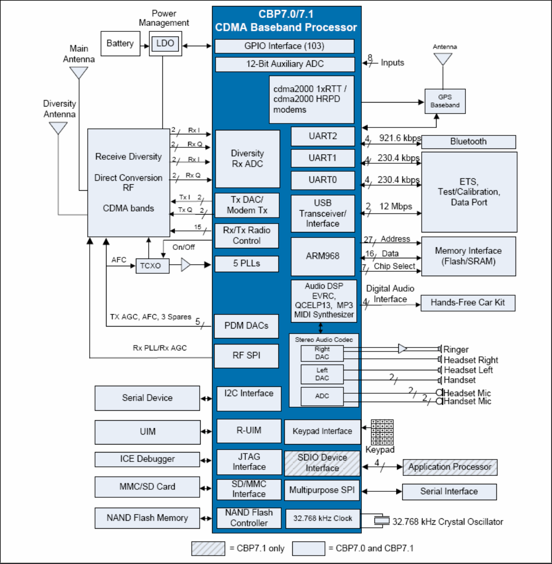
3.2 Hardware Specification
The hardware block diagram for MV84PG is shown as below:
The PCB for MV84PG is 8 layers.
11
4. Standards and Regulatory Compliance
4.1 Standards and certification
The EUT conforms to the following standards and certification requirements:
CDMA
❒ TIA/EIA IS-98E (CDMA2000 1x)
❒ TIA/EIA IS-866 (1xEV-DO)
FCC
❒ 47 CFR Part 1 - RF radiation exposure limits
❒ 47 CFR Part 2 - Equipment authorization
❒ 47 CFR Part 22 - Cellular
❒ 47 CFR Part 24 - PCS
12
4.2 FCC certification requirements.
According to the definition of mobile and fixed device is described in Part 2.1091(b), this device is a mobile device.
And the following conditions must be met:
1. The EUT is a mobile device; maintain at least a 20 cm separation between the EUT and the user’s body and must
not transmit simultaneously with any other antenna or transmitter.
2. The device is only for fixed operation mode. (A Class II Change would be required for near-body Host applications.)
3. A label with the following statements must be attached to the host end product: This device contains Tx FCC ID:
QVZ-MV84PG.
4. To comply with FCC regulations limiting both maximum RF output power and human exposure to RF radiation,
maximum antenna gain (including cable loss) must not exceed:
❒ Cellular band < 1.26 dBi
❒ PCS band < 1.56 dBi
5. This module must not transmit simultaneously with any other antenna or transmitter
6. The host end product must include a user manual that clearly defines operating requirements and conditions that
must be observed to ensure compliance with current FCC RF exposure guidelines.
For portable devices, in addition to the conditions 3 through 6 described above, a separate approval is required to
satisfy the SAR requirements of FCC Part 2.1093
If the device is used for other equipment that separate approval is required for all other operating configurations,
including portable configurations with respect to 2.1093 and different antenna configurations.
For this device, OEM integrators must be provided with labeling instructions of finished products. Please refer to
KDB784748 D01 v07, section 8. Page 6/7 last two paragraphs:
A certified modular has the option to use a permanently affixed label, or an electronic label. For a permanently
affixed label, the module must be labelled with an FCC ID - Section 2.926 (see 2.2 Certification (labelling
requirements) above). The OEM manual must provide clear instructions explaining to the OEM the labelling
requirements, options and OEM user manual instructions that are required (see next paragraph).
For a host using a certified modular with a standard fixed label, if (1) the module’s FCC ID is not
visible when installed in the host, or (2) if the host is marketed so that end users do not have
straightforward commonly used methods for access to remove the module so that the FCC ID of
the module is visible; then an additional permanent label referring to the enclosed module:
13
“Contains Transmitter Module FCC ID: XYZMODEL1” or “Contains FCC ID: XYZMODEL1” must
be used. The host OEM user manual must also contain clear instructions on how end users can
find and/or access the module and the FCC ID.
4.3 FCC RF exposure requirements
1. Radiated transmit power must be equal to or lower than that specified in the FCC Grant of Equipment Authorization
for FCC ID: QVZ-MV84PG.
2. To comply with FCC regulations limiting both maximum RF output power and human exposure to RF radiation,
maximum antenna gain (including cable loss) must not exceed:
❒ Cellular band < 1.26 dBi
❒ PCS band < 1.56 dBi
3. This module must not transmit simultaneously with any other antenna or transmitter.
4. To ensure compliance with all non-transmitter functions the host manufacturer is responsible for ensuring
compliance with the module(s) installed and fully operational. For example, if a host was previously authorized as an
unintentional radiator under the Declaration of Conformity procedure without a transmitter certified module and a
module is added, the host manufacturer is responsible for ensuring that the after the module is installed and
operational the host continues to be compliant with the Part 15B unintentional radiator requirements.