Chongqing Jinou Science and Technology Development BTM4504C1H Class1 Bluetooth Module User Manual
Chongqing Jinou Science & Technology Development Co., Ltd. Class1 Bluetooth Module
User Manual
BTM4504C1H
Bluetooth Module
Rev 2.4
Chongqing Jinou Science and Technology Development Co., Ltd.
website:www.jinoux.com
FCC ID:SI8-BTM4504C1H

Chongqing JINOU Science and Technology Development Co., Ltd.
BTM4504C1H
Page i
Contents
1. Features ............................................................................................................................... 2
2. Product Description ......................................................................................................... 2
3. Applications ....................................................................................................................... 2
4. Block Diagram ..................................................................................................................... 2
5. Pin Descriptions ............................................................................................................... 3
5.1 Device Terminal ......................................................................................................... 3
5.2 Device Terminal Functions ..................................................................................... 3
6. Electrical Specifications ............................................................................................. 4
6.1 Input/Output Terminal Characteristics ............................................................. 4
6.2 Auxilliary ADC ........................................................................................................... 5
6.3 Absolute Maximum ratings ....................................................................................... 5
6.4 Power Consumption(Don’t use AP) ................................................................... 5
7. Radio Characteristics – Basic Data Rate ............................................................... 5
7.1 Transmitter ................................................................................................................. 6
7.2 Receiver ....................................................................................................................... 6
8. UART Interface ................................................................................................................... 7
8.1 UART Bypass ................................................................................................................. 9
8.2 UART Configuration While RESET is Active ....................................................... 9
8.3 UART Bypass Mode ....................................................................................................... 9
8.4 Current Consumption in UART Bypass Mode ......................................................... 9
9. I/O Parallel Ports ........................................................................................................... 9
10. RESETB ................................................................................................................................. 10
10.1 Pin States on Reset ........................................................................................... 10
10.2 Status after Reset ............................................................................................. 10
11. Solder Profiles ............................................................................................................... 11
12. Physical Dimensions ....................................................................................................... 12
13. Guide for Antenna Radiation ....................................................................................... 13
Chongqing JINOU Science and Technology Development Co., Ltd.
BTM4504C1H
Page 2
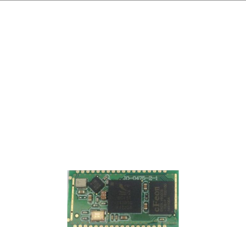
BTM4504C1H
Bluetooth Module Class 1
1. Features
1.1 Operating Frequency Band 2.40 GHz~2.48GHz unlicensed ISM Band
1.2 Class 1 type Output Power≤20 dBm ;Antenna gain≤1.5dBi
1.3 UART Host Interface
1.4 Low Voltage Power Supply, 2.7V to 3.6V
1.5 Nominal Supply Voltage at 3.3±0.1V
1.6 Low Power Modes Available: Park, Sniff, Hold and Deep Sleep
1.7 Size: 27.3mm×14.5 (unit:mm Error = ±0.2mm)
2. Product Description
The BC04 Bluetooth Module (BTM4504C1H) is a Class 1 Bluetooth module using
BlueCore4-External chipset from leading Bluetooth chipset supplier, Cambridge Silicon
Radio. It provides a fully compliant Bluetooth system for data and voice communications.
Interfaces with a host via USB or UART and support full data rate up to 3Mbps modulation
modes. Voice interface supported PCM protocol. The module and device firmware is fully
compliant with the Bluetooth specification v3.0.
3. Applications
3.1 PCs, PDAs
3.2 Computer Accessories (CF Cards, USB DonglesPCMCIA, RS232 Adaptors, etc.)
3.3 Mice, Keyboard, Joysticks
3.4 Cordless Phone
3.5 FAX, Printer Adaptors
3.6 Digital Camera
3.7 Access Points to LAN and/or Dial-up network
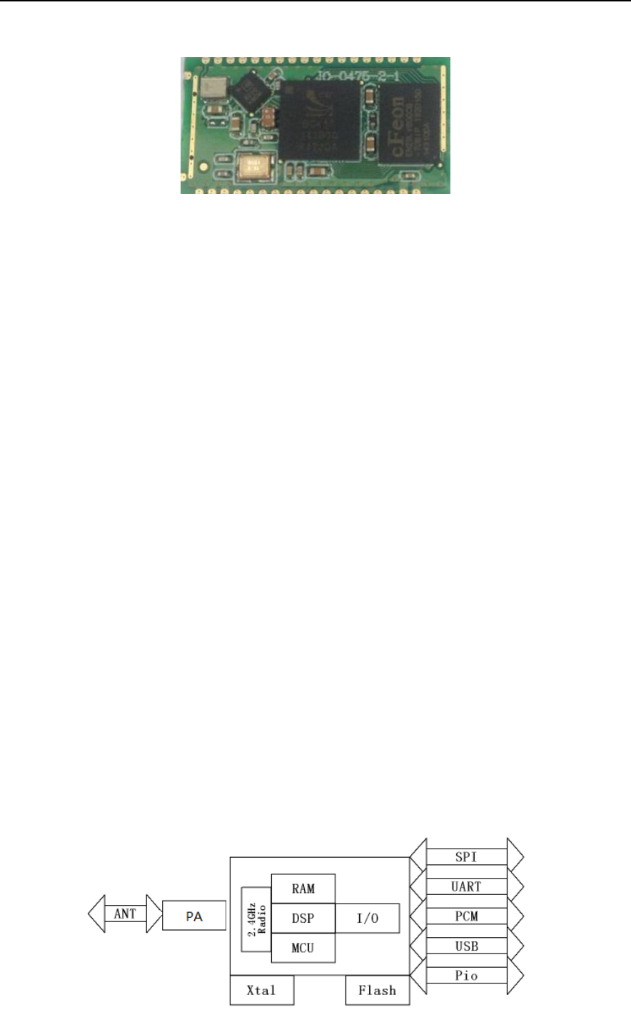
4. Block Diagram
Chongqing JINOU Science and Technology Development Co., Ltd.
BTM4504C1H
Page 3
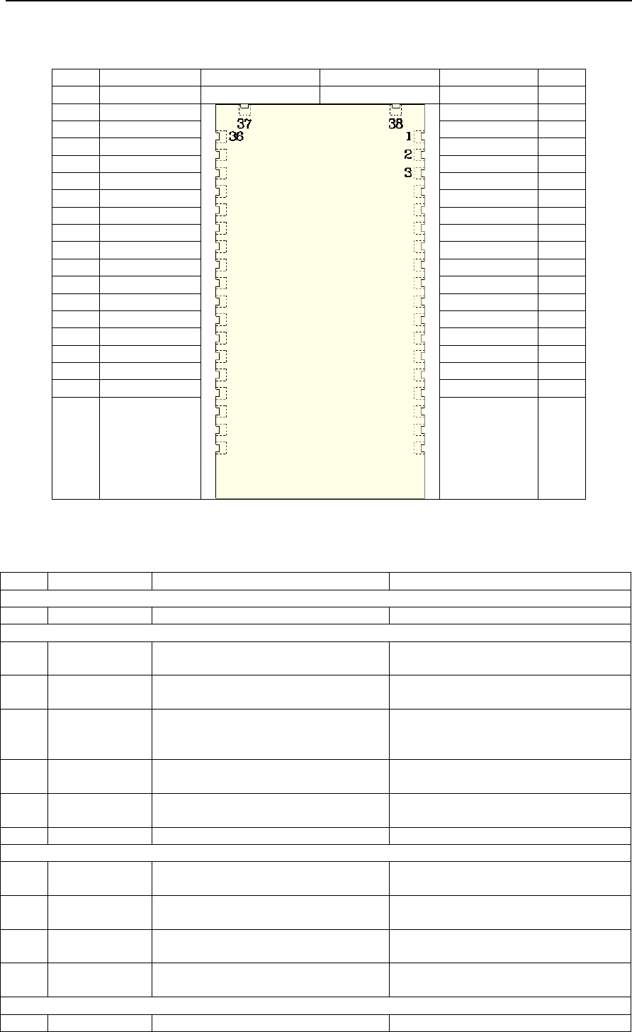
5. Pin Descriptions
5.1 Device Terminal
No.
Des
37
38
Des
No.
GND
GND
36
GND
ANT
1
35
GND
GND
2
34
GND
Pio2
3
33
GND
Pio3
4
32
Aio0
Pio4
5
31
Aio1
Pio5
6
30
RESET
Pio6
7
29
SPI-MISO
Pio7
8
28
SPI-CSB
Pio8
9
27
SPI-CLK
Pio9
10
26
SPI-MOSI
Pio10
11
25
UART-CTS
Pio11
12
24
UART-TX
USB-DN
13
23
UART-RTS
USB-DP
14
22
UART-RX
PCM-CLK
15
21
Vref-Filter
PCM-IN
16
20
Vcc
PCM-SYN
17
19
GND
PCM-OUT
18
5.2 Device Terminal Functions
PIN
NAME
TYPE
DESCRIPTION
1
ANT
Analogue
Single ended receiver input
24
UART_TX
CMOS output, tri-state, with weak
internal pull-up
UART data output
22
UART_RX
CMOS input with weak internal
pull-down
UART data input
23
UART_RTS
CMOS output, tri-state, with weak
internal pull-up
UART request to send active low
25
UART_CTS
CMOS input with weak
internal pull-down
UART clear to send active low
14
USB_DP
Bi-directional
USB data plus with selectable
internal 1.5k. pull-up resistor
13
USB_DN
Bi-directional
USB data minus
18
PCM_OUT
CMOS output, tri-state, with weak
internal pull-down
Synchronous data output
16
PCM_IN
CMOS input, with weak internal
pull-down
Synchronous data input
17
PCM_SYN
Bi-directional with weak internal
pull-down
Synchronous data sync
15
PCM_CLK
Bi-directional with weak
internal pull-down
Synchronous data clock
3
Pio2
Bi-directional with programmable
Programmable Input/Output Line

Chongqing JINOU Science and Technology Development Co., Ltd.
BTM4504C1H
Page 4
strength internal pull-up/down
4
Pio3
Bi-directional with programmable
strength internal pull-up/down
Programmable Input/Output Line
5
Pio4
Bi-directional with programmable
strength internal pull-up/down
Programmable input/output line or
Optionally BT_Priority/Ch_Clk output
for co-existence signalling
6
Pio5
Bi-directional with programmable
strength internal pull-up/down
Programmable input/output line or
Optionally BT_Active output for
co-existence signalling
7
Pio6
Bi-directional with programmable
strength internal pull-up/down
Programmable input/output line or
Optionally WLAN_Active/Ch_Data input
for co-existence signalling
8
Pio7
Bi-directional with programmable
strength internal pull-up/down
Programmable Input/Output Line
9
Pio8
Bi-directional with programmable
strength internal pull-up/down
Programmable Input/Output Line
10
Pio9
Bi-directional with programmable
strength internal pull-up/down
Programmable Input/Output Line
11
Pio10
Bi-directional with programmable
strength internal pull-up/down
Programmable Input/Output Line
12
Pio11
Bi-directional with programmable
strength internal pull-up/down
Programmable Input/Output Line
32
Aio0
Bi-directional
Programmable input/output line
31
Aio1
Bi-directional
Programmable input/output line
30
RESET
CMOS input with weak internal pull-up
internal pull-up Reset if low. Input
debounced so must be low for >5ms to
cause a reset
28
SPI_CSB
CMOS input with weak internal pull-up
Chip select for Synchronous Serial
Interface active low
27
SPI_CLK
CMOS input with weak internal
pull-down
Serial Peripheral Interface clock
26
SPI_MOSI
CMOS input with weak internal
pull-down
Serial Peripheral Interface data
input
29
SPI_MISO
CMOS output, tri-state, with weak
internal pull-down
Serial Peripheral Interface data
output
21
Vref-Filter
Filter Capacitor for 1.8V
20
Vcc
Power Supply
+3.3V Power Supply。
--
GND
(Other)
Ground
6. Electrical Specifications
6.1 Input/Output Terminal Characteristics
Digital Terminals
Min
Typ
Max
Unit
Input Voltage Levels
VIL input logic level low 2.7V ≤ Vcc ≤ 3.0V
-0.4
-
+0.8
V
VIH input logic level high
0.7Vcc
-
Vcc+0.4
V
Output Voltage Levels
VOL output logic level low
(lo = 4.0mA), 2.7V ≤ Vcc ≤ 3.0V
-
-
0.2
V
VOH output logic level high
(lo = -4.0mA), 2.7V ≤ Vcc ≤ 3.0V
Vcc-0.2
-
-
V
Input and Tri-state Current with
Strong pull-up
-100
-40
-10
μA
Strong pull-down
+10
+40
+100
μA
Weak pull-up
-5.0
-1.0
-0.2
μA
Weak pull-down
+0.2
+1.0
+5.0
μA

Chongqing JINOU Science and Technology Development Co., Ltd.
BTM4504C1H
Page 5
I/O pad leakage current
-1
0
+1
μA
CI Input Capacitance
1.0
-
5.0
pF
6.2 Auxilliary ADC
Auxiliary ADC
Min
Typ
Max
Unit
Resolution
-
-
8
Bits
Input voltage range (LSB size = Vref/255)
0
-
Vref
V
Accuracy INL(Guaranteed monotonic)
-1
-
1
LSB
Accuracy DNL (Guaranteed monotonic)
0
-
1
LSB
Offset
-1
-
1
LSB
Gain Error
-0.8
-
0.8
%
Input Bandwidth
-
100
-
kHz
Conversion time
-
2.5
-
μs
Sample rate(a)
-
-
700
Samples/s
6.3 Absolute Maximum ratings
Absolute maximum ratings for supply voltage and voltages on digital and analogue
pins of the Module are listed below; exceeding these values will cause permanent damage.
Parameter
Min
Max
Unit
Peak current of power supply
0
75
mA
Voltage at digital pins
-0.3
3.6
V
Voltage at POWER pin
2.7
3.6
V
6.4 Power Consumption(Don’t use AP)
Operation Mode
Connection
Type
UART Rate
(kbps)
Average
Unit
Page scan
-
115.2
0.42
mA
Inquiry and page scan
-
115.2
0.76
mA
ACL No traffic
Master
115.2
4.60
mA
ACL With file transfer
Master
115.2
10.3
mA
ACL No traffic
Slave
115.2
17.0
mA
ACL With file transfer
Slave
115.2
24.7
mA
ACL 40ms sniff
Master
38.4
2.40
mA
ACL 1.28s sniff
Master
38.4
0.37
mA
SCO HV1
Master
38.4
39.2
mA
SCO HV3
Master
38.4
20.3
mA
SCO HV3 30ms sniff
Master
38.4
19.8
mA
ACL 40ms sniff
Slave
38.4
2.11
mA
ACL 1.28s sniff
Slave
38.4
0.42
mA
Parked 1.28s beacon
Slave
38.4
0.20
mA
SCO HV1
Slave
38.4
39.1
mA
SCO HV3
Slave
38.4
24.8
mA
SCO HV3 30ms sniff
Slave
38.4
19.0
mA
Standby Host connection(a)
-
38.4
40
uA
Reset (RESETB low)(a)
-
-
34
uA
(a) Low power mode on the linear regulator is entered and exited automatically when
the chip enters/leaves Deep Sleep mode .
(b) Add 0~100mA if use AP.
7. Radio Characteristics – Basic Data Rate
Important Notes

Chongqing JINOU Science and Technology Development Co., Ltd.
BTM4504C1H
Page 6
BlueCore4 meets the Bluetooth v3.0 + EDR specification when used in a suitable
application circuit between -40°C and +105°C.
Tx output is guaranteed to be unconditionally stable over the guaranteed temperature
range.
7.1 Transmitter
Radio Characteristics Vcc = 3.3V Temperature = +20°C
Min
Typ
Max
Bluetooth
Specification
Unit
Maximum RF transmit power(1)(2)
-
15
-
0 to +20(3)
dBm
Variation in RF power over temperature range with
compensation enabled (±)(4)
-
1.5
-
-
dB
Variation in RF power over temperature range with
compensation disabled (±)(4)
-
2
-
-
dB
RF power control range
-
35
-
≥16
dB
RF power range control resolution (5)
-
0.5
-
-
dB
20dB bandwidth for modulated carrier
-
780
-
≤1000
kHz
Adjacent channel transmit power F=F0 ±2MHz(6)(7)
-
-40
-
≤-20
dBm
Adjacent channel transmit power F=F0 ±3MHz(6)(7)
-
-45
-
≤-40
dBm
Adjacent channel transmit power F=F0>±3MHz(6)(7)
-
-50
-
≤-40
dBm
Δf1avg .Maximum Modulation.
-
165
-
140<
Δf1avg
<175
kHz
Δf2max .Minimum Modulation.
-
150
-
≥115
kHz
Δf2avg / Δf1avg
-
0.97
-
≥0.80
-
Initial carrier frequency tolerance
-
6
-
±75
kHz
Drift Rate
-
8
-
≤20
kHz
/50μS
Drift (single slot packet)
-
7
-
≤25
kHz
Drift (five slot packet)
-
9
-
≤40
kHz
2nd Harmonic content
-
-65
-
≤-30
dBm
3rd Harmonic content
-
-45
-
≤-30
dBm
Notes:
(1) BlueCore4 firmware maintains the transmit power to be within the Bluetooth v3.0 +
EDR specification limits.
(2) Measurement made using a PSKEY_LC_MAX_TX_POWER setting corresponds to a
PSKEY_LC_POWER_TABLE power table entry of 63.
(3) Class 1 RF transmit power range, Bluetooth v3.0 + EDR specification.
(4) To some extent these parameters are dependent on the matching circuit used, and its
behaviour over temperature. Therefore these parameters may be beyond CSR’s direct
control.
(5) Resolution guaranteed over the range -5dB to -25dB relative to maximum power for
Tx Level >20.
(6) Measured at F0= 2441MHz.
(7) Up to three exceptions are allowed in the Bluetooth v3.0 + EDR specification.
BlueCore4 is guaranteed to meet the ACP performance as specified by the Bluetooth v3.0
+ EDR specification.
7.2 Receiver
Radio Characteristics Vcc = 3.3V Temperature = +20°C
Frequency
(GHz)
Min
Typ
Max
Bluetooth
Specification
Unit
Sensitivity at 0.1% BER
for all packet types
2.402
-
-84
-
≤-70
dBm
2.441
-
-84
-
2.480
-
-85
-
Maximum received signal at 0.1% BER
-
10
-
≤-20
dBm
Frequency
(GHz)
Min
Typ
Max
Bluetooth
Specification
Unit
Chongqing JINOU Science and Technology Development Co., Ltd.
BTM4504C1H
Page 7
Continuous power required to block
Bluetooth reception (for sensitivity of
-67dBm with 0.1% BER) measured at the
unbalanced port of the balun.
30 - 2000
-
TBD
-
≤-10
dBm
2000 - 2400
-
TBD
-
≤-27
2500 - 3000
-
TBD
-
≤-27
3000 - 3300
-
TBD
-
≤-10
C/I co-channel
-
6
-
≤11
dB
Adjacent channel selectivity C/I F=F0 +1MHz(1) (2)
-
-5
-
≤0
dB
Adjacent channel selectivity C/I F=F0 −1MHz(1) (2)
-
-4
-
≤0
dB
Adjacent channel selectivity C/I F=F0 +2MHz(1) (2)
-
-38
-
≤-30
dB
Adjacent channel selectivity C/I F=F0 −2MHz(1) (2)
-
-23
-
≤-20
dB
Adjacent channel selectivity C/I F≥F0 +3MHz(1) (2)
-
-45
-
≤-40
dB
Adjacent channel selectivity C/I F≤F0 −5MHz(1) (2)
-
-44
-
≤-40
dB
Adjacent channel selectivity C/I F=FImage(1) (2)
-
-22
-
≤-9
dB
Maximum level of intermodulation interferers (3)
-
-30
-
≥-39
dBm
Spurious output level (4)
-
TBD
-
-
dBm/Hz
Notes:
(1) Up to five exceptions are allowed in the Bluetooth v3.0 + EDR specification. BlueCore4
is guaranteed to meet the C/I performance as specified by the Bluetooth v3.0 + EDR
specification.
(2) Measured at F0 = 2441MHz
(3) Measured at f1-f2 = 5MHz. Measurement is performed in accordance with Bluetooth RF
test RCV/CA/05/c. i.e. wanted signal at -64dBm
(4) Measured at the unbalanced port of the balun. Integrated in 100kHz bandwidth and
then normalized to 1Hz. Actual figure is typically below TBD dBm/Hz except for peaks
of -52dBm inband at 2.4GHz and ≤80dBm at 3.2GHz
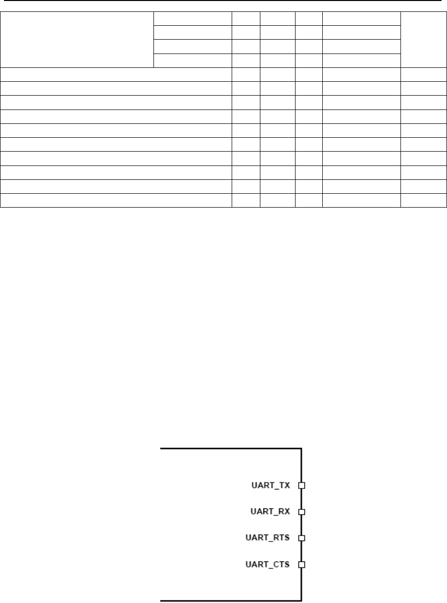
8. UART Interface
BlueCore4-External Universal Asynchronous Receiver Transmitter (UART) interface
provides a simple mechanism for communicating with other serial devices using the RS232
standard(1).
BlueCore4-External
Figure 11.12: Universal Asynchronous Receiver
Four signals are used to implement the UART function, as shown in Figure 11.12. When
BlueCore4-External is connected to another digital device, UART_RX and UART_TX transfer
data between the two devices. The remaining two signals, UART_CTS and UART_RTS, can be
used to implement RS232 hardware flow control where both are active low indicators. All
UART connections are implemented using CMOS technology and have signalling levels of
0V and Vcc.
UART configuration parameters, such as Baud rate and packet format, are set using
BlueCore4-External software.
Chongqing JINOU Science and Technology Development Co., Ltd.
BTM4504C1H
Page 8
Notes:
In order to communicate with the UART at its maximum data rate using a standard PC,
an accelerated serial port adapter card is required for the PC.
(1) Uses RS232 protocol but voltage levels are 0V to VDD_USB, (requires external
RS232 transceiver chip)
Parameter
Possible Values
Baud Rate
Minimum
1200 Baud (≤2%Error)
9600 Baud (≤1%Error)
Maximum
3.0MBaud (≤1%Error)
Flow Control
RTS/CTS or None
Parity
None, Odd or Even
Number of Stop Bits
1 or 2
Bits per channel
8
Table 11.7: Possible UART Settings
The UART interface is capable of resetting BlueCore4-External upon reception of a
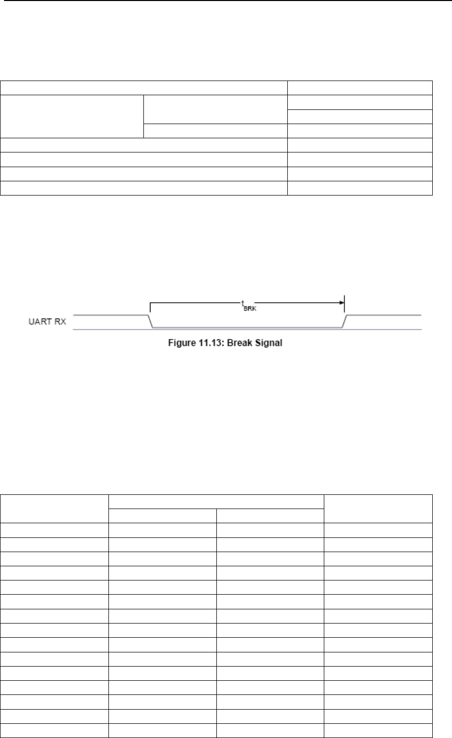
break signal. A Break is identified by a continuous logic low (0V) on the UART_RX terminal,
as shown in Figure 11.13. If tBRK is longer than the value, defined by the PS Key
PSKEY_HOST_IO_UART_RESET_TIMEOUT, (0x1a4), a reset will occur.
This feature allows a host to initialise the system to a known state. Also,
BlueCore4-External can emit a Break character that may be used to wake the Host.
Note:
The DFU boot loader must be loaded into the Flash device before the UART or USB
interfaces can be used.This initial flash programming can be done via the SPI.
Table 11.3 shows a list of commonly used Baud rates and their associated values for
the Persistent Store Key PSKEY_UART_BAUD_RATE (0x204). There is no requirement to use
these standard values. Any Baud rate within the supported range can be set in the
Persistent Store Key according to the formula in Equation 11.7.
Baud Rate = PSKEY_UART_BAUD_RATE / 0.004096
Equation 11.7: Baud Rate
Baud Rate
Persistent Store Value
Error
Hex
Dec
1200
0x0005
5
1.73%
2400
0x000a
10
1.73%
4800
0x0014
20
1.73%
9600
0x0027
39
-0.82%
19200
0x004f
79
0.45%
38400
0x009d
157
-0.18%
57600
0x00ec
236
0.03%
76800
0x013b
315
0.14%
115200
0x01d8
472
0.03%
230400
0x03b0
944
0.03%
460800
0x075f
1887
-0.02%
921600
0x0ebf
3775
0.00%
1382400
0x161e
5662
-0.01%
1843200
0x1d7e
7550
0.00%
2764800
0x2c3d
11325
0.00%
Chongqing JINOU Science and Technology Development Co., Ltd.
BTM4504C1H
Page 9
Table 11.8: Standard Baud Rates
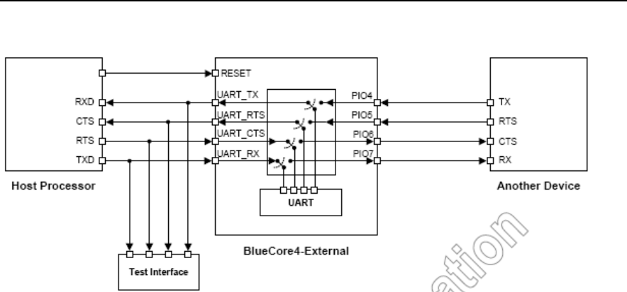
8.1 UART Bypass
Figure 11.14: UART Bypass Architecture
8.2 UART Configuration While RESET is Active
The UART interface for BlueCore4-External while the chip is being held in reset is
tri-state. This will allow the user to daisy chain devices onto the physical UART bus.
The constraint on this method is that any devices connected to this bus must tri-state
when BlueCore4-External reset is de-asserted and the firmware begins to run.
8.3 UART Bypass Mode
Alternatively, for devices that do not tri-state the UART bus, the UART bypass mode
on BlueCore4-External can be used. The default state of BlueCore4-External after reset
is de-asserted, this is for the host UART bus to be connected to the BlueCore4-External
UART, thereby allowing communication to BlueCore4-External via the UART.
In order to apply the UART bypass mode, a BCCMD command will be issued to
BlueCore4-External upon this, it will switch the bypass to PIO[7:4] as shown in Figure
11.14. Once the bypass mode has been invoked, BlueCore4-External will enter the deep
sleep state indefinitely.
In order to re-establish communication with BlueCore4-External, the chip must be
reset so that the default configuration takes affect.
It is important for the host to ensure a clean Bluetooth disconnection of any active
links before the bypass mode is invoked. Therefore it is not possible to have active
Bluetooth links while operating the bypass mode.
8.4 Current Consumption in UART Bypass Mode
The current consumption for a device in UART Bypass Mode is equal to the values quoted
for a device in standby mode.
9. I/O Parallel Ports
Fifteen lines of programmable bi-directional input/outputs (I/O) are provided.
PIO[11:8] and PIO[3:0] are powered from Vcc. PIO[7:4] are powered from Vcc. AIO [2:0]
are powered from Vref.
PIO lines can be configured through software to have either weak or strong pull-ups
or pull-downs. All PIO lines are configured as inputs with weak pull-downs at reset.
PIO[0] and PIO[1] are normally dedicated to RXEN and TXEN respectively, but they
are available for general use.
Any of the PIO lines can be configured as interrupt request lines or as wake-up lines
from sleep modes. PIO[6] or PIO [2] can be configured as a request line for an external
clock source. This is useful when the clock to BlueCore4-External is provided from a

Chongqing JINOU Science and Technology Development Co., Ltd.
BTM4504C1H
Page 10
system application specific integrated circuit (ASIC).
BlueCore4-External has three general purpose analogue interface pins, AIO[0], AIO[1]
and AIO[2]. These are used to access internal circuitry and control signals. One pin
is allocated to decoupling for the on-chip band gap reference voltage, the other three
may be configured to provide additional functionality.
Auxiliary functions available via these pins include an 8-bit ADC and an 8-bit DAC.
Typically the ADC is used for battery voltage measurement. Signals selectable at these
pins include the band gap reference voltage and a variety of clock signals; 48, 24, 16,
8MHz and the XTAL clock frequency. When used with analogue signals the voltage range
is constrained by the analogue supply voltage (1.8V). When configured to drive out digital
level signals (clocks) generated from within the analogue part of the device, the output
voltage level is determined by Vref (1.8V).
Important Note:
CSR cannot guarantee that terminal functions PIOs remain the same. Please refer to
the software release note for the implementation of these PIO lines, as they are firmware
build specific.
10. RESETB
BlueCore4 Module may be reset from several sources: power on reset, a UART break
character or via a software configured watchdog timer.
The power on reset occurs when the VDD_CORE supply falls below typically 1.5V and
is released when VDD_CORE rises above typically 1.6V.
At reset the digital I/O pins are set to inputs for bi-directional pins and outputs
are tri-stated. The PIOs have weak pull-downs.
Following a reset, BlueCore4-External assumes the maximum XTAL_IN frequency, which
ensures that the internal clocks run at a safe (low) frequency until BlueCore4-External
is configured for the actual XTAL_IN frequency. If no clock is present at XTAL_IN, the
oscillator in BlueCore4-External free runs, again at a safe frequency.
10.1 Pin States on Reset
Table 11.15 shows the pin states of BlueCore4-External on reset.
Pin Name
State: BlueCore4-External
PIO[6:2]
Input with weak pull-down
UART_TX
Output tri-stated with weak pull-up
UART_RX
Input with weak pull-down
UART_RTS
Output tri-stated with weak pull-up
UART_CTS
Input with weak pull-down
SPI_CSB
Input with weak pull-up
SPI_CLK
Input with weak pull-down
SPI_MOSI
Input with weak pull-down
SPI_MISO
Output tri-stated with weak pull-down
AIO[1]
Output, driving low
Table 11.15: Pin States of BlueCore4-External on Reset
10.2 Status after Reset
The chip status after a reset is as follows:
Warm Reset: Baud rate and RAM data remain available
Cold Reset(1): Baud rate and RAM data not available
Note:
(1) Cold Reset constitutes one of the following:
Power cycle
System reset (firmware fault code)
Chongqing JINOU Science and Technology Development Co., Ltd.
BTM4504C1H
Page 11
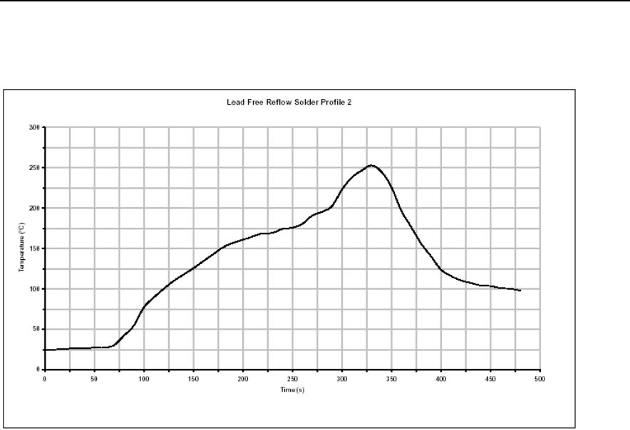
11. Solder Profiles
Composition of the solder ball: Sn 95.5%, Ag 4.0%, Cu 0.5%
Typical Lead-Free Re-flow Solder Profile
Key features of the profile:
Initial Ramp = 1-2.5°C/sec to 175°C±25°C equilibrium
Equilibrium time = 60 to 180 seconds
Ramp to Maximum temperature (250°C) = 3°C/sec max.
Time above liquidus temperature (217°C): 45-90 seconds
Device absolute maximum reflow temperature: 260°C
Devices will withstand the specified profile. Lead-free devices will withstand up to
three reflows to a maximum temperature of 260°C.
Notes:They need to be baked prior to mounting。
Chongqing JINOU Science and Technology Development Co., Ltd.
BTM4504C1H
Page 12
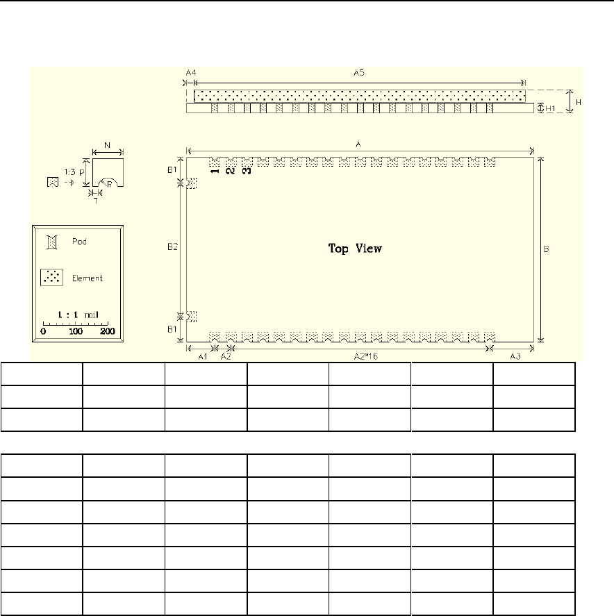
12. Physical Dimensions
A
A1
A2
A3
A4
A5
unit
1075
87
50
138
22
1025
mil
27.31
2.21
1.27
3.51
0.56
26.04
mm
B
B1
B2
H
H1
Unit
570
80
410
74
32
mil
14.48
2.03
10.41
1.88
0.81
mm
N
P
T
R
Unit
32
28
6
10
mil
0.81
0.71
0.15
0.25
mm
while L > 100mil Error = ±10mil,while L<= 100mil Error = ±10%

Chongqing JINOU Science and Technology Development Co., Ltd.
BTM4504C1H
Page 13
13. Guide for Antenna Radiation
In order to achieve longest communication range, please keep the area surrounding
antenna free of grounding or metal housing.
Modular Approval:
The BTM4504C1H module is designed to comply with the FCC statement. FCC ID is
SI8BTM4504C1H. The host system using BTM4504C1H, should have label indicated
it contain modular’s FCC ID SI8BTM4504C1H.
*RF warning for Mobile device:
This equipment complies with FCC radiation exposure limits set forth for an uncontrolled
environment. This equipment should be installed and operated with minimum distance
20cm between the radiator & your body.
§ 15.19 Labelling requirements.
This device complies with part 15 of the FCC Rules. Operation is subject to the
following two conditions: (1) This device may not cause harmful interference, and (2)
this device must accept any interference received, including interference that may
cause undesired operation.
§ 15.21 Information to user.
Any Changes or modifications not expressly approved by the party responsible for
compliance could void the user's authority to operate the equipment.
§ 15.105 Information to the user.
Note: This equipment has been tested and found to comply with the limits for a
Class B digital device, pursuant to part 15 of the FCC Rules. These limits are designed
to provide reasonable protection against harmful interference in a residential
installation. This equipment generates uses and can radiate radio frequency energy and,
if not installed and used in accordance with the instructions, may cause harmful
interference to radio communications. However, there is no guarantee that interference
will not occur in a particular installation. If this equipment does cause harmful
interference to radio or television reception, which can be determined by

Chongqing JINOU Science and Technology Development Co., Ltd.
BTM4504C1H
Page 1 of 17
turning the equipment off and on, the user is encouraged to try to correct the
interference by one or more of the following measures:
-Reorient or relocate the receiving antenna.
-Increase the separation between the equipment and receiver.
-Connect the equipment into an outlet on a circuit different from that to which the
receiver is connected.
-Consult the dealer or an experienced radio/TV technician for help.
Chongqing Jinou Science & Technology Development Co., Ltd.
Address : D1-802, Overseas Students Pioneer Park, No.71 Kecheng Rd, Jiulongpo
District, 400039, Chongqing
Tel:86-23-68903066/68842136
Fax:86-23-68644164
mail:yf@jinoux.com jinou-lisa@foxmail.com whf@jinoux.com
website:www.jinoux.com
the OEM integrator is still responsible for testing their end-product for any additional compliance requirements
required with this module installed
IMPORTANT NOTE: In the event that these conditions cannot be met (for example certain laptop configurations
or co-location with another transmitter), then the FCC authorization is no longer considered valid and the FCC
ID can not be used on the final product. In these circumstances, the OEM integrator will be responsible for re-
evaluating the end product (including the transmitter) and obtaining a separate FCC authorization.
Manual Information To the End User
The OEM integrator has to be aware not to provide information to the end user regarding how to install or remove
this RF module in the user’s manual of the end product which integrates this module.