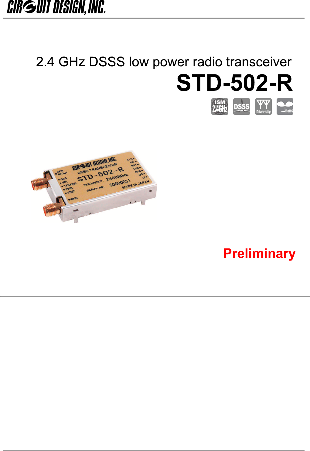
Circuit Design STD502R 2.4 GHz DSSS low power radio transceiver User Manual OG STD 502 R appr
Circuit Design, Inc. 2.4 GHz DSSS low power radio transceiver OG STD 502 R appr
User manual
OPERATION GUIDE.
OG_STD-502-R_v09e Circuit Design, Inc.
1
Operation Guide
Version 0.9 (Feb. 2013)
CIRCUIT DESIGN, INC.
7557-1 Hotaka, Azumino
Nagano 399-8303 JAPAN
Tel: 0263-82-1024
Fax: 0263-82-1016
e-mail: info@circuitdesign.jp
http://www.circuitdesign.jp

OPERATION GUIDE.
OG_STD-502-R_v09e Circuit Design, Inc.
2
1. Outline
The STD-502-R operates in the 2.4 GHz band available worldwide. Designed to be embedded in
equipment, this radio transceiver module was developed for industrial applications that require stable
and reliable operation. With battery operation, it achieves line of sight radio communication beyond
300 m.
Besides using highly noise-resistant direct-sequence spread spectrum (DSSS) modulation, the
module has a true diversity receiver function for preventing signal dropout due to multipath fading.
This ensures highly stable and reliable radio communication in the congested 2.4. GHz ISM band.
The transceiver uses a transparent input/output interface, enabling users to use their own protocols.
In addition, the transceiver can transmit data that includes long consecutive identical bits that cannot
be transmitted with conventional radio modules.
2. Features and applications
Features
Direct sequence spectrum (DSSS)
True diversity receiving
Communication range 300 m (LOS)
Low power operation 10 mW, 3.3 V, 68 mA
Data rate 19.2 kbps
Built-in data frame coincidence detection function
Operating temperature range -20 to +65°C
Compliance with European EN300 440, American FCC Part 15.247, and Japan ARIBSTD-T-66
regulations
Applications
Remote control of industrial equipment
Industrial telemetry and monitoring systems

OPERATION GUIDE.
OG_STD-502-R_v09e Circuit Design, Inc.
3
3. Specifications
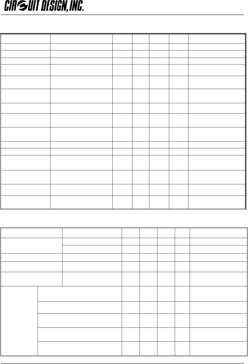
General specifications
* All values are taken with the antenna ports terminated with 50 ohm and at 25 degree C +/- 5 degree C unless otherwise
noted
Item Specification Unit Remarks
Applicable standard EN300 440-1, FCC part 15.247,
ARIB STD-T66
Communication method Simplex
Emission type Direct sequence spread spectrum
Modulation method FSK
Number of channels 77ch (Ch 0 to Ch 76)
Antenna connection RP-SMAJ
Dimensions 50 × 30 × 9 ( W x D x H ) mm RP-SMAJ and power & signal
connector pins excluded
Weight 24 g
Interface specifications
Item Specification Unit Remarks
Baud rate: 19.2 kbps (typ.), No parity
Character: 8 bits, Stop bit : 2 bits
Baud rate
19.2 / 38.4 / 57.6 kbps
Input TXD L = 0 to 0.25
H = Vref - 0.4 to Vref V UART *1
Interface for module
setting
Output RX
D
L = 0 to 0.25
H = Vref - 0.4 to Vref V UART *1
RX data output DO L = 0 to 0.25
H = Vref - 0.4 to Vref VRX data out using a transparent
method *1
CLK for data input/output CLK L = 0 to 0.25
H = Vref - 0.4 to Vref V*1
TX data input DI L = 0 to 0.25
H = Vref - 0.4 to Vref VTX data out using a transparent
method *1
Diversity receiving
antenna DIV L = 0 to 0.25
H = Vref - 0.4 to Vref VShows on which antenna data is
received. *1
TX/RX switching terminal TXRXSEL L = 0 to 0.3
H = Vcc - 0.4 to Vcc V H: RX / L: TX
RF standby terminal STBY L = 0 to 0.3
H = Vcc - 0.4 to Vcc V H: Standby / L: RF operation
Reset terminal RST L = 0 to 0.25
H = Vcc - 0.4 to Vcc V Reset with L for more than 100 us
Communication level
reference terminal VREF 3.1 - 5.5 V
Vref (a terminal for applying a
reference voltage consistent with
the external communication level)
*1 " H" level depends on the voltage level applied to the communication level reference terminal.
OPERATION GUIDE.
OG_STD-502-R_v09e Circuit Design, Inc.
4
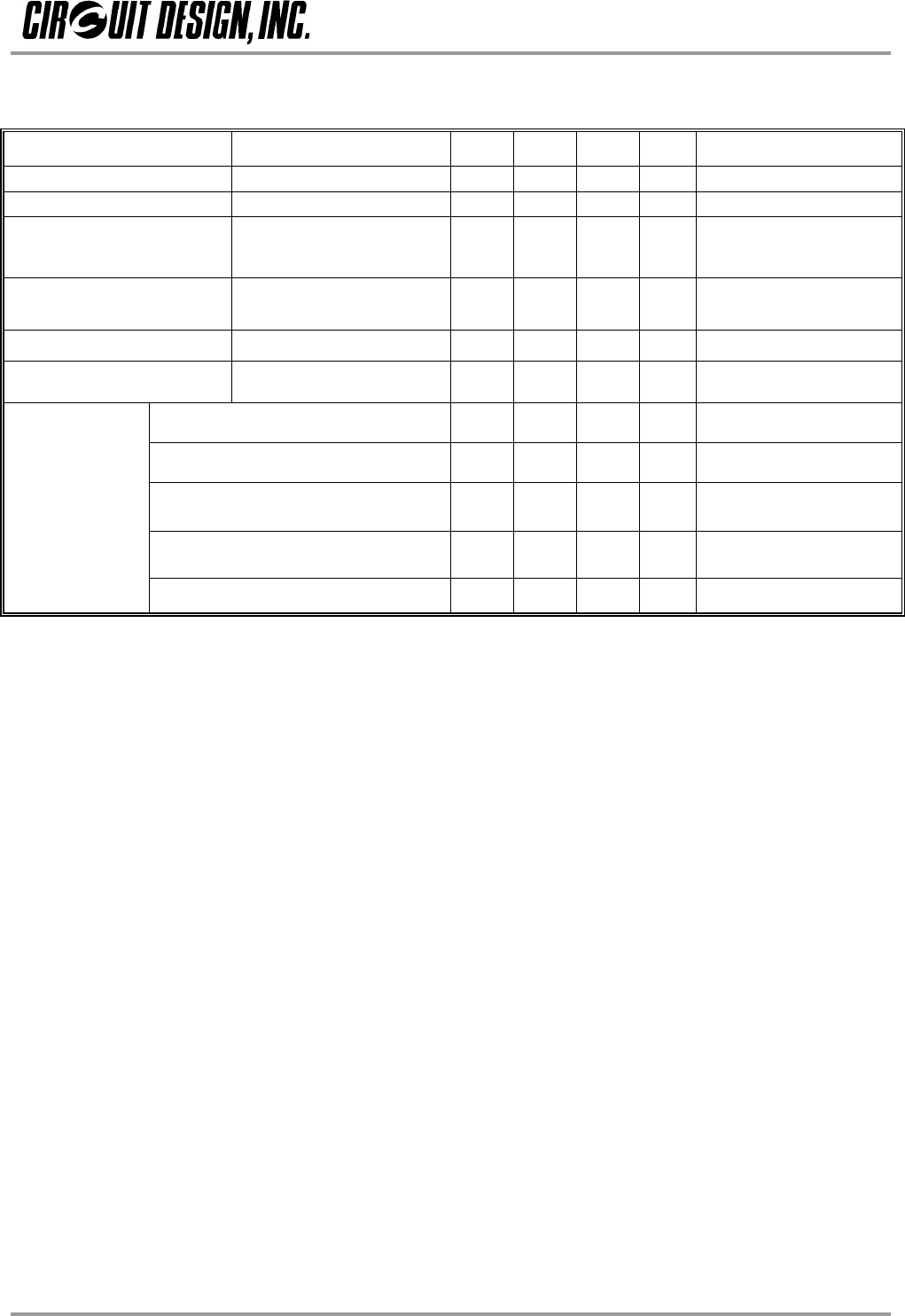
Electrical specification (Common)
Item Specification MIN TYP MAX Unit Remarks
Operating voltage 3.3 5.5 V
TX current Vcc = 3.3 V 66 mA at 10 mW
RX current Vcc = 3.3 V 75 mA
TX/RX frequency
range 2.4 GHz band 2402.5 2478.5 MHzRefer to the frequency
table
Operating
temperature range -20°C to + 65°C -20 65 °C No dew condensation
Storage
temperature range -30°C to +90°C -30 90 °C No dew condensation
Aging rate < +/- 1 ppm / year -1 1 ppm TX / RX Lo frequency
Initial frequency
tolerance
+/- 10 ppm within one
year from shipment -10 10 ppm Transmission frequency
Oscillation type Fractional N PLL
controlled VCO
Frequency stability +/- 10 ppm (-20 to +65°C) -10 10 ppm Reference temp. = 25 C
Channel spacing 1 MHz 1 MHz
Data bit rate 19.2 kbps 19.2 kbps can be changed with the
command
Chip rate 288 kcps 288 kcps can be changed with the
command
Number of chips M-sequence
(111101010001100) 15 bit
PLL reference
frequency 26 26 MHzTCXO : NT2520SA
Electrical specification (Transmitter)
Item Specification MIN TYP MAX Unit Remarks
-10 to +55°C /all channels 10 mW
Output power -20 to +65°C /all channels 2 TBD
Spurious emission TBD dBm EN300 440-1 compliant
Adjacent channel power TBD dBc EN300 440-1 compliant
Occupied frequency
bandwidth TBD kHz EN300 440-1 compliant
Power on -> command reception 42 ms Power on in the TX mode
Command reception -> TX 5 ms Country code reception ->
stable RF output
Frequency change 3 ms Command transmission ->
Stable RF output
RX to TX 2 ms Terminal input -> Stable
operation
Actuation
time
Recovery from standby 1.2 ms Standby -> stable RF
output
OPERATION GUIDE.
OG_STD-502-R_v09e Circuit Design, Inc.
5
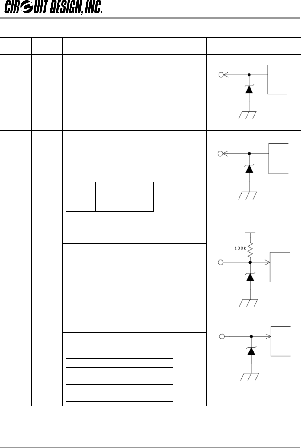
Electrical specification (Receiver)
Item Specification MIN TYP MAX Unit Remarks
Reception method Low IF
Maximum input level -13 dBm
Receiver sensitivity
(BER, 9.6 kbps) -20 to + 65°C /all channels -93 dBm error rate = < 1 %
Receiver sensitivity
(BER, 19.2 kbps) -20 to + 65°C /all channels -93 dBm error rate = < 1 %
Blocking EN300 440-1 compliant -45 dBm 2 signal test, 1% error
Spurious radiation
(1st Lo) dBm
Power on -> County code reception 42 ms Power on in the RX mode
Command reception -> RX 5 ms
Frequency change 3 ms Command reception -> RX
start
TX to RX 2 ms Terminal input -> Stable
operation
Actuation
time
Recovery from standby 1.2 Standby -> RX start
OPERATION GUIDE.
OG_STD-502-R_v09e Circuit Design, Inc.
6
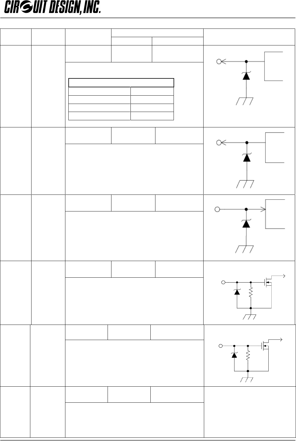
4. Terminal specifications
Terminal Terminal Input/ Input/Output level (V)
No. name Output Low Hi Internal equivalent circuit
Output 0 to 0.25 Vref -0.4 to Vref
1 CLK
TX: Synchronous CLK for TX data input
RX: Synchronous CLK for RX data output
Output 0 to 0.25 Vref -0.4 to Vref
2 DIV
This terminal shows which of the two receiving
terminals received the signal actually used for data
output. .
DIV Data receiving
terminal
L RF in
H RF in/out
Input 0 - 0.25 Vcc -0.4 to Vcc
3 RST
The initialization terminal for coincidence detection
function*.
The internal ASIC is reset with ‘L’ level for more
than 100 μs.
Normally set this terminal to ‘H’.
* For details of the frame coincidence detection function,
refer to “Frame coincidence detection function” on page
16.
Input 0 to 0.25 Vref -0.4 to Vref
4 TXD
The input terminal for serial communication.
Settings for serial communication
Baud rate 19.2 kbps
Character bits 8 bits
Parity none
Stop bits 2 bits
Terminal
Level
Translator
Terminal
Level
Translator
Terminal
Level
Translator
Terminal
Level
Translator
OPERATION GUIDE.
OG_STD-502-R_v09e Circuit Design, Inc.
7
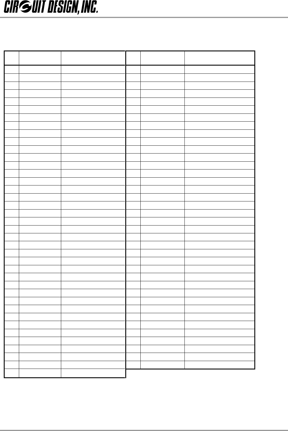
Terminal Terminal Input/ Input/Output level (V)
No. name Output Low Hi Internal equivalent circuit
Output 0 to 0.25 Vref -0.4 to Vref
5 RXD
The output terminal for serial communication.
Settings for serial communication
Baud rate 19.2 kbps
Character bits 8 bits
Parity none
Stop bits 2 bits
Output 0 to 0.25 Vref -0.4 to Vref
6 DO
The RX data output terminal.
Outputs RX data in synchronization with the clock
from the RX-CLK.
The DO data should be read at the rising clock
edge of the RX-CLK
Input 0 to 0.25 Vref -0.4 to Vref
7 DI
The TX data input terminal.
Inputs TX data in synchronization with the clock
from the TX-CLK.
Data should be set to the DI at the falling clock
edge of the TX-CLK.
Input 0 - 0.3 Vcc -0.4 to Vcc
8TXRX
SEL
The terminal for switching the TX mode and RX
mode.
Setting this terminal to ‘L’ enables the TX mode
and setting to ‘H’ enables the RX mode.
Input 0 - 0.3 Vcc -0.4 to Vcc
9 NC Sets the STD-502-R into RF-standby state.
Setting this terminal to L enables normal operation
and setting to H enables RF-standby.
RF-standby can be used to reduce the current
consumption.
Input 3.1 5.5
10 Vref The input terminal for interface reference voltage.
Communication can be performed using the
voltage level applied to this terminal.
Terminal
Termin
1
M
Ω
C
P
U
Terminal
Level
Translator
Level
Translator
Level
Translator
Terminal
Termin
al
1
M
Ω
C
P
U
OPERATION GUIDE.
OG_STD-502-R_v09e Circuit Design, Inc.
8
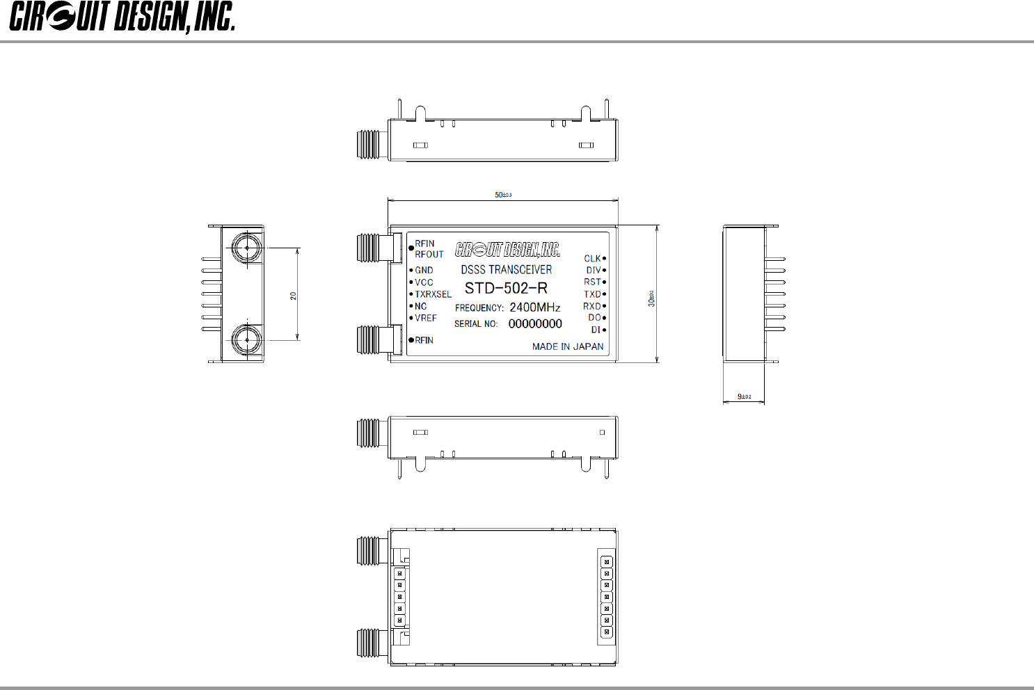
5. Frequency table
CH
No.
Channel No.
(Hex) Frequency [MHz] CH
No.
Channel No.
(Hex) Frequency [MHz]
000 2402.5 39 27 2441.5
101 2403.5 40 28 2442.5
202 2404.5 41 29 2443.5
303 2405.5 42 2A 2444.5
404 2406.5 43 2B 2445.5
505 2407.5 44 2C 2446.5
606 2408.5 45 2D 2447.5
707 2409.5 46 2E 2448.5
808 2410.5 47 2F 2449.5
909 2411.5 48 30 2450.5
10 0A 2412.5 49 31 2451.5
11 0B 2413.5 50 32 2452.5
12 0C 2414.5 51 33 2453.5
13 0D 2415.5 52 34 2454.5
14 0E 2416.5 53 35 2455.5
15 0F 2417.5 54 36 2456.5
16 10 2418.5 55 37 2457.5
17 11 2419.5 56 38 2458.5
18 12 2420.5 57 39 2459.5
19 13 2421.5 58 3A 2460.5
20 14 2422.5 59 3B 2461.5
21 15 2423.5 60 3C 2462.5
22 16 2424.5 61 3D 2463.5
23 17 2425.5 62 3E 2464.5
24 18 2426.5 63 3F 2465.5
25 19 2427.5 64 40 2466.5
26 1A 2428.5 65 41 2467.5
27 1B 2429.5 66 42 2468.5
28 1C 2430.5 67 43 2469.5
29 1D 2431.5 68 44 2470.5
30 1E 2432.5 69 45 2471.5
31 1F 2433.5 70 46 2472.5
32 20 2434.5 71 47 2473.5
33 21 2435.5 72 48 2474.5
34 22 2436.5 73 49 2475.5
35 23 2437.5 74 4A 2476.5
36 24 2438.5 75 4B 2477.5
37 25 2439.5 76 4C 2478.5
38 26 2440.5
OPERATION GUIDE.
OG_STD-502-R_v09e Circuit Design, Inc.
9
6. External dimensions

OPERATION GUIDE
OG_STD-502-R_v09e Circuit Design, Inc.
10
Regulatory compliance information
Regulatory Statement for FCC
This device complies with part 15 of the FCC Rules. Operation is subject to the following two conditions:
(1) This device may not cause harmful interference, and (2) this device must accept any interference
received, including interference that may cause undesired operation.
Caution: Any changes or modifications not expressly approved by the party responsible for product
compliance could void the user's authority to operate the equipment.
Note: This equipment has been tested and found to comply with the limits for a Class B digital device,
pursuant to part 15 of the FCC Rules. These limits are designed to provide reasonable protection against
harmful interference in a residential installation. This equipment generates, uses and can radiate radio
frequency energy and, if not installed and used in accordance with the instructions, may cause harmful
interference to radio communications. However, there is no guarantee that interference will not occur in a
particular installation. If this equipment does cause harmful interference to radio or television reception,
which can be determined by turning the equipment off and on, the user is encouraged to try to correct the
interference by one or more of the following measures:
—Reorient or relocate the receiving antenna.
—Increase the separation between the equipment and receiver.
—Connect the equipment into an outlet on a circuit different from that to which the receiver is connected.
—Consult the dealer or an experienced radio/TV technician for help.
Labeling:
FCC ID: V9X-STD502R
The proposed FCC ID label format is to be placed on the module. If FCC ID is not visible when the
module is installed into the system, “Contains FCC ID: V9X-STD502R shall be placed on the outside of
final host system.
Caution: Exposure to radio frequency radiation
To comply with FCC RF exposure compliance requirements, a separation distance of at least 20 cm must
be maintained between the antenna of this device and all persons. This device must not be co-located or
operating in conjunction with any other antenna or transmitter, except in accordance with FCC multi-
transmitter product procedures.
Antenna
Only those antennas with same type and lesser gain filed under this FCC ID number can be used with
this device.
The antenna used this module is as follows;
Antenna Type & Antenna Gain;
Sleeve Antenna, 2dBi
Loop PCB Antenna, 1.89dBi
Coaxial Antenna, 1.67dBi
Instructions to OEM Integrators
The final system integrator must ensure there is no instruction provided in the user manual or customer
documentation indicating how to install or remove the transmitter module.
To comply with FCC RF exposure compliance requirements, a separation distance of at least 20 cm must
be maintained between the antenna of this device and all persons. This device must not be co-located or
operating in conjunction with any other antenna or transmitter, except in accordance with FCC multi-
transmitter product procedures.

OPERATION GUIDE
OG_STD-502-R_v09e Circuit Design, Inc.
11
DoC and restrictions for CE
Hereby, Circuit Design, Inc., declares that this STD-502-R is in compliance with the essential
requirements and other relevant provisions of Directive 1999/5/EC.
This equipment is marked with the symbol and can be used throughout the European community.
This indicates compliance with the R&TTE Directive 1999/5/EC and meets the relevant parts of following
technical specifications:
EN 300 440-2, Electromagnetic compatibility and Radio spectrum Matters (ERM);Short range devices;
Radio equipment to be used in the 1 GHz to 40 GHz frequency range; Part 2: Harmonized EN
covering the essential requirements of article 3.2 of the R&TTE Directive
EN 301 489-17, Electromagnetic Compatibility and Radio spectrum Matters (ERM); Electromagnetic
Compatibility (EMC) standard for radio equipment and services; Part 17: Specific Conditions for
Wideband Data and HYPERLAN Equipment.
EN 60950-1, Safety of Information Technology Equipment.
EN 62311, Assessment of electronic and electrical equipment related to human exposure restrictions for
electromagnetic fields (0 Hz-300 GHz).
Remark:
This module is for a portable application. The OEM integrator will need to conduct full EMC testing in
accordance with EN301 489-17 in the final use configuration.
Caution: Exposure to radio frequency radiation
This device must not be co-located or operating in conjuction with any other antenna or transmitter.

OPERATION GUIDE
OG_STD-502-R_v09e Circuit Design, Inc.
12
Important notice
Customers are advised to consult with Circuit Design sales representatives before ordering.
Circuit Design believes the provided information is accurate and reliable. However, Circuit Design
reserves the right to make changes to this product without notice.
Circuit Design products are neither designed nor intended for use in life support applications where
malfunction can reasonably be expected to result in significant personal injury to the user. Any use of
Circuit Design products in such safety-critical applications is understood to be fully at the risk of the
customer and the customer must fully indemnify Circuit Design, Inc for any damages resulting from
any improper use.
As the radio module communicates using electronic radio waves, there are cases where transmission
will be temporarily cut off due to the surrounding environment and method of usage. The manufacturer
is exempt from all responsibility relating to resulting harm to personnel or equipment and other
secondary damage.
The manufacturer is exempt from all responsibility relating to secondary damage resulting from the
operation, performance and reliability of equipment connected to the radio module.
Copyright
All rights in this operation guide are owned by Circuit Design, Inc. No part of this document may be
copied or distributed in part or in whole without the prior written consent of Circuit Design, Inc.
Cautions
Do not use the equipment within the vicinity of devices that may malfunction as a result of electronic
radio waves from the radio module.
Communication performance will be affected by the surrounding environment, so communication tests
should be carried out before actual use.
Ensure that the power supply for the radio module is within the specified rating. Short circuits and
reverse connections may result in overheating and damage and must be avoided at all costs.
Ensure that the power supply has been switched off before attempting any wiring work.
The case is connected to the GND terminal of the internal circuit, so do not make contact between the
'+' side of the power supply terminal and the case.
When batteries are used as the power source, avoid short circuits, recharging, dismantling, and
pressure. Failure to observe this caution may result in the outbreak of fire, overheating and damage to
the equipment. Remove the batteries when the equipment is not to be used for a long period of time.
Failure to observe this caution may result in battery leaks and damage to the equipment.
Do not use this equipment in vehicles with the windows closed, in locations where it is subject to direct
sunlight, or in locations with extremely high humidity.
The radio module is neither waterproof nor splash proof. Ensure that it is not splashed with soot or
water. Do not use the equipment if water or other foreign matter has entered the case.
Do not drop the radio module or otherwise subject it to strong shocks.
Do not subject the equipment to condensation (including moving it from cold locations to locations with
a significant increase in temperature.)
Do not use the equipment in locations where it is likely to be affected by acid, alkalis, organic agents or
corrosive gas.
Do not bend or break the antenna. Metallic objects placed in the vicinity of the antenna will have a
great effect on communication performance. As far as possible, ensure that the equipment is placed
well away from metallic objects.
The GND for the radio module will also affect communication performance. If possible, ensure that the
case GND and the circuit GND are connected to a large GND pattern.
Warnings
Do not take apart or modify the equipment.
Do not remove the product label (the label attached to the upper surface of the module.) Using a
module from which the label has been removed is prohibited.