City Theatrical 5995 2400MHz Multiverse Module5995 User Manual Multiverse Module OEM
CITY THEATRICAL, INC. 2400MHz Multiverse Module5995 Multiverse Module OEM
Multiverse Module OEM User Manual

Multiverse® Module
OEM User Manual
Rev 1.9
© 2017 City Theatrical, Inc.
Multiverse devices are covered by U.S. patent #7,432,803.
Other patents pending.

599x Series
www.citytheatrical.com
2
Table of Contents
1 Revision History ..................................................................................................................... 6
2 Introduction ............................................................................................................................ 7
2.1 Features ......................................................................................................................... 7
2.2 Part Numbers ................................................................................................................. 8
3 Specifications ......................................................................................................................... 9
3.1 Regulatory Specifications ............................................................................................. 11
3.1.1 FCC Part 15 .......................................................................................................... 11
3.1.2 Radio Frequency Notifications .............................................................................. 11
3.1.3 FCC Notifications .................................................................................................. 11
3.1.4 Industry Canada Notification ................................................................................. 12
4 OEM Installation .................................................................................................................. 13
4.1 OEM Labeling Requirements ....................................................................................... 13
4.1.1 FCC Compliance Statement (United States) ......................................................... 13
4.1.2 IC Statement ......................................................................................................... 13
4.2 Approved Antennas ...................................................................................................... 14
5 Recommended Layout Decals ............................................................................................. 15
5.1 Layout Notes ................................................................................................................ 16
6 Signal Pinout ........................................................................................................................ 17
7 OEM Interfaces .................................................................................................................... 18
7.1 I2C ................................................................................................................................ 18
7.1.1 I2C Accessible Data .............................................................................................. 20
7.1.2 I2C Protocol ........................................................................................................... 20
7.1.2.1 Strings ............................................................................................................ 20
7.1.2.2 Termination and Overrun ............................................................................... 20
7.1.2.3 Repeated Reads ............................................................................................ 21
7.1.2.4 Repeated Writes ............................................................................................ 21
7.1.2.5 Slot Array ....................................................................................................... 21
7.1.2.6 Timing diagrams ............................................................................................. 21
7.1.3 I2C Register Descriptions ...................................................................................... 21
7.1.3.1 (0x0046) I2C Attention Register ..................................................................... 21
7.1.3.2 (0x0047) I2C RDM Proxy Traffic Enable ........................................................ 22

599x Series
www.citytheatrical.com
3
7.1.3.3 (0x0049) I2C RDM Response ........................................................................ 22
7.1.3.4 (0x004A) I2C RDM PD ................................................................................... 23
7.2 SPI ................................................................................................................................ 23
7.2.1 SPI Protocol .......................................................................................................... 23
7.3 UART ............................................................................................................................ 24
7.4 Recommended Configurations ..................................................................................... 24
7.4.1 Minimal .................................................................................................................. 24
7.4.2 Basic ...................................................................................................................... 25
7.4.3 Advanced .............................................................................................................. 26
8 Tape and Reel Information .................................................................................................. 28
9 Reflow Profile ....................................................................................................................... 29

599x Series
www.citytheatrical.com
4
List of Tables
Table 1: Revision History 6
Table 2: Part Numbers 8
Table 3: Absolute Maximum Ratings 9
Table 4: Physical Characteristics 9
Table 5: ESD Ratings 9
Table 6: Recommended Operating Conditions 9
Table 7: Power Consumption Summary 10
Table 8: DC Characteristics 10
Table 9: RF Characteristics 10
Table 10: Interfaces 10
Table 11: Timing Characteristics 10
Table 12: Approved Antennas 14
Table 13: Pinout Descriptions 17
Table 14: I2C Addresses 18
Table 15: I2C Accessible Data 20
Table 16: I2C Attention Data Bytes 22
Table 17: I2C Attention Reason Codes 22
Table 18: I2C RDM Response Data Bytes 22
Table 19: Synchronous Serial Interface (SSI) Characteristics 23

599x Series
www.citytheatrical.com
5
List of Figures
Figure 1: 5990 Decal 15
Figure 2: 5994 Decal 15
Figure 3: 5991/5995 Decal 16
Figure 4: 5990 Side View 16
Figure 5: 5994 Side View 16
Figure 6: 5991/5995 Side View 16
Figure 7: Example Board Layout 16
Figure 8: Example Stencil Design 16
Figure 9: I2C Specification 21
Figure 10: SSI Timing 23
Figure 11: Minimal Configuration Block Diagram 25
Figure 12: Basic Configuration Block Diagram 25
Figure 13: Advanced Configuration Block Diagram 26
599x Series
www.citytheatrical.com
6
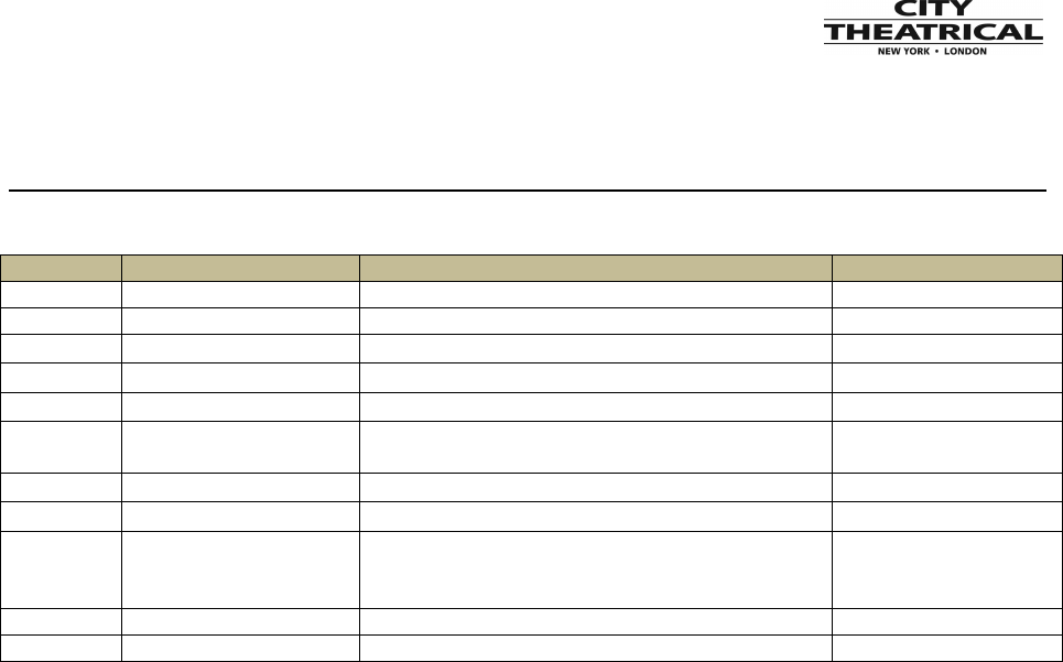
1 Revision History
Table 1: Revision History
Revision
Date
Description
Author/Changed
1.0
May 8th, 2017
Preliminary release of Footprint and pin info
P. Kleissler
1.1
August 15th 2017
Added Electrical Characteristics and Protocol
D. Smith/P. Kleissler
1.2
August 24th 2017
Updated Table 4 packaging
P. Kleissler
1.3
November 6th 2017
Added ID 7&8 to Table 12
A. Joo
1.4
November 6th 2017
Added text to Introduction
P. Kleissler
1.4
November 6th 2017
Updates to cover page; revised intro for
naming consistency
J. Morreale
1.5
November 13th 2017
Updated Table 12 ID8 gain to 11dBi
A. Joo
1.6
December 4th 2017
Updated Table 14 and added I2C Attention
P. Kleissler
1.7
December 6th 2017
Added Integration block diagrams
Added more I2C register descriptions
Added Configuration Block Diagrams
P. Kleissler
1.8
December 19th 2017
Added required OEM wording on antenna
P. Kleissler
1.9
January 23rd 2018
Added OEM requirements as per FCC review
P. Kleissler

599x Series
www.citytheatrical.com
7
2 Introduction
City Theatrical's newest version of the Multiverse® Modules provides unprecedented levels of
data transmission in a tiny package, and at the lowest cost yet seen in the entertainment lighting
industry for professional quality wireless DMX.
Multiverse Modules are best suited for lighting equipment manufacturers who are interested in
adding wireless DMX to their products. Due to low cost, increased data transport, and ease of
design integration, the Multiverse Module marks the first time that the implementation of a
wireless DMX chip in every DMX device is possible.
The Multiverse Module is available in two frequency ranges, 900MHz (for use in the Americas)
and 2.4GHz (for use worldwide). Each frequency version can include a PCB trace antenna or
not. All versions have a U.FL connector to connect to external antennas. Consult Table 2 for
part numbers.
The implementation of Multiverse Modules is simple because they are available on reels for
surface mounting. The engineer can opt to integrate in one of three ways: Minimal, Basic or
Advanced.
The Minimal Integration Method replaces the DMX input circuitry with the module. The
Multiverse module will deliver DMX/RDM directly via TTL UART signals. In this configuration,
the Multiverse module will appear as a separate RDM device from the OEM product. This
method provides an easy path to add the Multiverse module to existing products without major
re-design of the product.
The Basic Integration Method replaces the DMX/RDM input circuitry, provides a DMX and RDM
stack and appears as a single integrated OEM RDM device. This configuration also allows for
seamless DMX wired and wireless operation without any additional hardware to be
implemented. This is the recommended integration method because it provides the most benefit
to the end user with the lowest implementation cost.
The Advanced Integration Method provides all of the features of the other two methods, but
enables multiple universes to be processed. This method of integration is required when you
need access to more than a single universe, or need to transport alternate start code (ASC)
data.
2.1 Features
Supports ANSI E1.11 DMX512-A and E1.20 RDM
Supports unidirectional alternate start codes
Up to 2,560 DMX slots
Non-Interfering RDM
Adaptive frequency hopping modes
Low Latency < 7ms
599x Series
www.citytheatrical.com
8
Source frame size/rate matching
Backwards compatible with SHoW DMX Neo, Neo Max systems
With or without PCB trace antenna
External antenna supported via U.FL/IPEX antenna connector on all models
900MHz and 2.4GHz models
I2C Slave configuration from OEM host
SPI interface
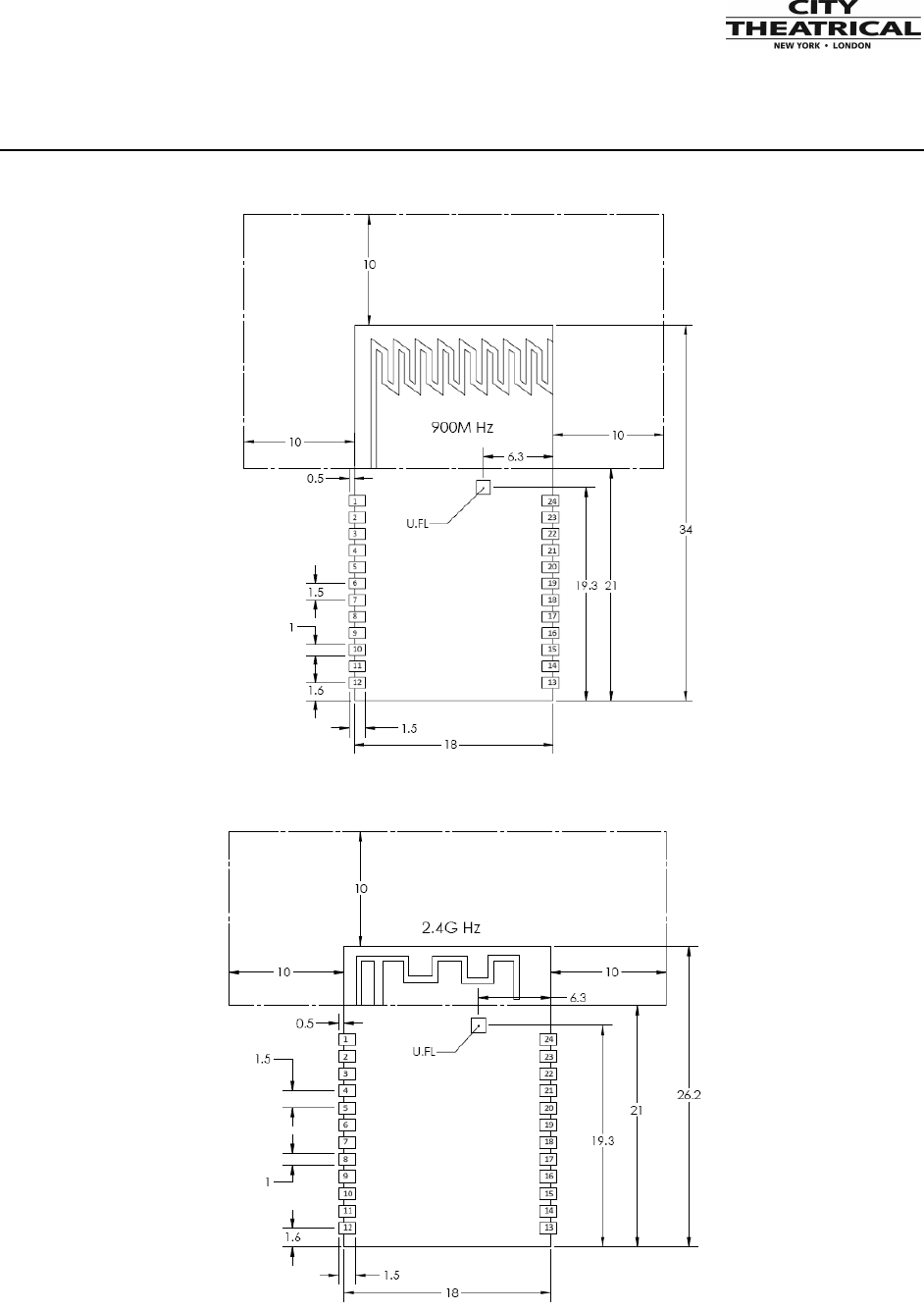
Small footprint (900MHz, 18x34mm; 2.4GHz, 18x26.2mm; 900/2.4 No PCB Antenna
18x21mm)
Same pinout for all models, design for largest, install any
Firmware updatable over air or by OEM system via I2C
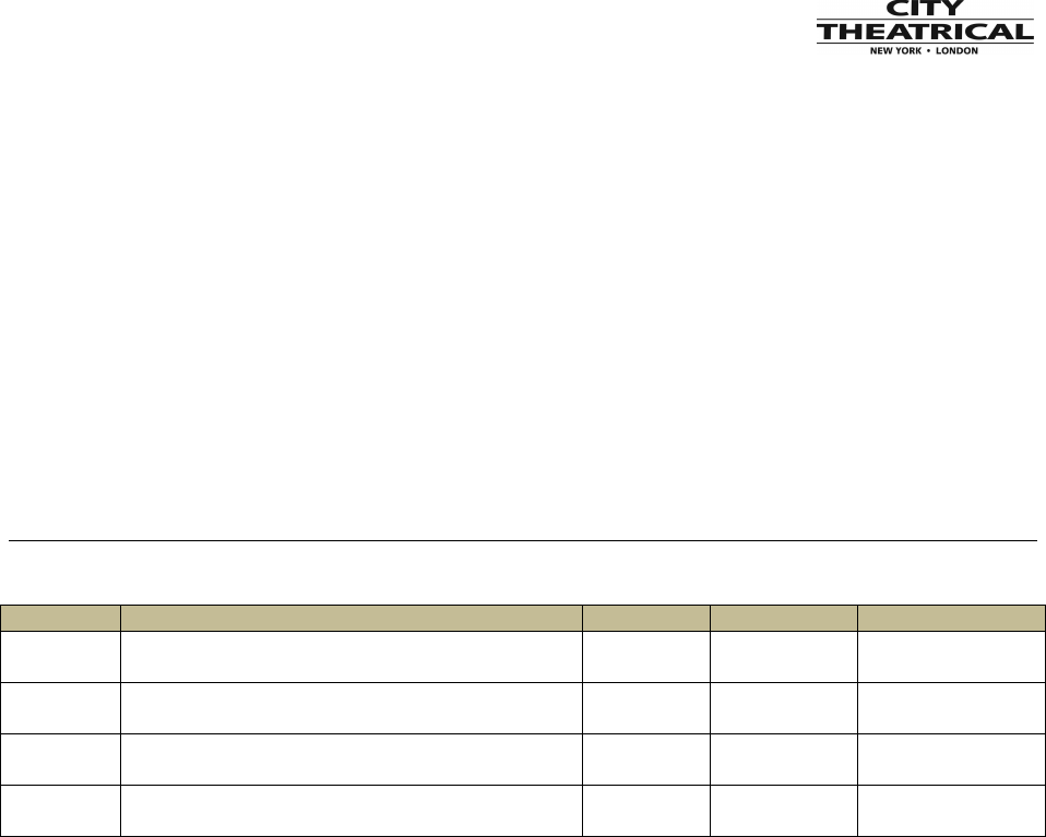
2.2 Part Numbers
Table 2: Part Numbers
Model #
Description
FCC ID:
IC:
Size
5990
900MHz Multiverse Module Internal &
External Antenna (DTS)
VU65990
7480A-5990
18mm x 34mm
5991
900MHz Multiverse Module External Antenna
Only (DTS)
VU65991
7480A-5991
18mm x 21mm
5994
2.4GHz Multiverse Module Internal &
External Antenna (FHSS)
VU65994
7480A-5994
18mm x 26.2mm
5995
2.4GHz Multiverse Module External Antenna
Only (FHSS)
VU65995
7480A-5995
18mm x 21mm
599x Series
www.citytheatrical.com
9
3 Specifications
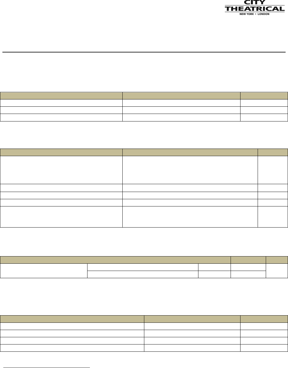
Table 3: Absolute Maximum Ratings
Over operating free-air temperature range (unless otherwise noted)
1
MIN
MAX
UNIT
Supply Voltage
-0.3
VCC + 0.3, max3.6
V
Voltage on any pin
-0.3
VCC + 0.3, max3.6
V
Storage Temperature
-40
150
°C
Table 4: Physical Characteristics
UNIT
Size
5990: 18 x 34 x 2.8
5991: 18 x 21 x 2.8
5994: 18 x 26.2 x 2.8
5995: 18 x 21 x 2.8
mm
OEM Interface
PCB SMD 2 x 12 castellated edge
Antenna Connector
U.FL/IPEX
Moisture Sensitivity Level
3
Packaging
5990: Tape & Reel 13” 56mm, 780/reel
5994: Tape & Reel 13” 44mm, 780/reel
5991/5995: Tape & Reel 13” 32mm, 780/reel
Table 5: ESD Ratings
VALUE
UNIT
VESD Electrostatic Discharge
Human body Model (HBM)2
All Pins
±3500
V
Charged device model (CDM)3
All Pins
±1250
Table 6: Recommended Operating Conditions
Over operating free-air temperature range
MIN
MAX
UNIT
Ambient Temperature
-40
85
°C
Operating Supply Voltage (VCC)
3.10
3.36
V
Rising Supply voltage slew rate
0
100
mV/µs
Falling Supply voltage slew rate
0
20
mV/µs
1
Stresses beyond those listed under Absolute Maximum Ratings may cause permanent damage to the
module. There are stress ratings only, and functional operation of the device at these or any other
conditions beyond those indicated under Recommended Operating Conditions is not implied. Exposure
to absolute-maximum-rated conditions for extended periods may affect device reliability.
2
Per ANSI/ESDA/JEDEC JS001.
3
Per JESD22-C101
599x Series
www.citytheatrical.com
10
Table 7: Power Consumption Summary
Transmit and receive measurements made with maximum power settings. Different RF modes
will affect power consumption.
PARAMETER
TEST CONDITIONS
MODULE
TYP
UNIT
Current Consumption
Sleep
5990/5991
?
mA
5994/5995
?
mA
Transmitter
5990/5991
30
mA
5994/5995
80
mA
Receiver
5990/5991
25
mA
5994/5995
25
mA
Table 8: DC Characteristics
MIN
MAX
UNIT
VOH at 4mA Load
2.72
V
VOL at 4mA Load
0.28
V
VIH
Lowest interface input voltage
reliably interpreted as a High
0.8
V
VIL
Highest interface input voltage
reliably interpreted as a Low
0.2
V
Table 9: RF Characteristics
TRANSMITTER CHARACTERISTICS
UNIT
Frequency Range
5990/5991: 902 ~ 928
5994/5995: 2.40 ~ 2.483
MHz
GHz
Rated Transmit Power
17 +0.25
dBm
Encryption
AES-128
Security
User Password
RECEIVER CHARACTERISTICS
Sensitivity
dBm
Error Checking
CRC32
Forward Error Correction
Cross-Packet
Modulations
5990 / 5991
DTS
5994 / 5995
FHSS
Table 10: Interfaces
OEM INTERFACE
SPEED
SPI
4 Wire Slave
4Mbps max
I2C
2 Wire Slave
400Kbps max
UART
DMX TTL with Driver control
250Kbps
Table 11: Timing Characteristics
MIN
MAX
UNIT
599x Series
www.citytheatrical.com
11
nReset low duration
1
µs
Active → Sleep
µs
Sleep → Active
µs
3.1 Regulatory Specifications
3.1.1 FCC Part 15
This equipment has been tested and found to comply with the limits for a Class B digital device,
pursuant to part 15 of the FCC Rules. These limits are designed to provide reasonable
protection against harmful interference in a residential installation. This equipment generates
uses and can radiate radio frequency energy and, if not installed and used in accordance with
the instructions, may cause harmful interference to radio communications. However, there is no
guarantee that interference will not occur in a particular installation. If this equipment does
cause harmful interference to radio or television reception, which can be determined by turning
the equipment off and on, the user is encouraged to try to correct the interference by one or
more of the following measures:
Re-orient or re-locate the receiving antenna.
Increase the separation between the equipment and receiver.
Connect the equipment into an outlet on a circuit different from that to which the receiver
is connected.
Consult the dealer or an experienced radio/TV technician for help.
THIS DEVICE COMPLIES WITH PART 15 OF THE FCC RULES. OPERATION IS SUBJECT
TO THE FOLLOWING TWO CONDITIONS: (1) THIS DEVICE MAY NOT CAUSE HARMFUL
INTERFERENCE, AND (2) THIS DEVICE MUST ACCEPT ANY INTERFERENCE RECEIVED,
INCLUDING INTERFERENCE THAT MAY CAUSE UNDESIRED OPERATION.
3.1.2 Radio Frequency Notifications
3.1.3 FCC Notifications
RF Radiation: The Product is an intentional radiator of Radio Frequency (RF) energy. In order
to limit RF exposure to personnel in the immediate area, the Product should be located and
installed such that a separation of at least 20 centimeters is maintained between the Product’s
antenna and personnel in the vicinity of the device. The antenna used for this transmitter must
not be co-located or operated in conjunction with any other antenna or transmitter.
Modification warning: Caution - changes or modifications to this equipment, not expressly
approved by City Theatrical, Inc. could void the user’s authority to operate the equipment.

599x Series
www.citytheatrical.com
12
3.1.4 Industry Canada Notification
This Class B digital apparatus complies with Canadian ICES-003. Operation is subject to the
following two conditions: (1) this device may not cause interference, and (2) this device must
accept any interference, including interference that may cause undesired operation of the
device.
Cet appareil numérique de la classe B est conforme à la norme NMB-003 du Canada.
Le présent appareil est conforme aux CNR d'Industrie Canada applicables aux appareils radio
exempts de licence. L'exploitation est autorisée aux deux conditions suivantes : (1) l'appareil ne
doit pas produire de brouillage, et (2) l'utilisateur de l'appareil doit accepter tout brouillage
radioélectrique subi, même si le brouillage est susceptible d'en compromettre le
fonctionnement.

599x Series
www.citytheatrical.com
13
4 OEM Installation
These modules are limited to OEM installations only.
The OEM integrator is responsible for ensuring that the end user has no manual instructions to
remove or install the modules.
The modules are limited to installation in mobile or fixed applications, according to Part
2.1091(b)
Separate approval is required for all other operating configurations, including portable
configurations with respect to Part 2.1093 and different antenna configurations.
4.1 OEM Labeling Requirements
The OEM integrator is required to have the following statements in the end product’s user’s
manual.
4.1.1 FCC Compliance Statement (United States)
This device complies with Part 15 of the Federal Communications Commission (FCC) Rules.
Operation is subject to the following two conditions:
This device may not cause harmful interference.
This device must accept any interference received, including interference that may cause
undesired operation.
CAUTION:
Changes or modifications to this unit not expressly approved by the party responsible for
compliance could void the user’s authority to operate this equipment.
4.1.2 IC Statement
This device complies with Industry Canada’s license-exempt RSSs. Operation is subject to the
following two conditions:
(1) This device may not cause interference; and
(2) This device must accept any interference, including interference that may cause undesired
operation of the device.
Le présent appareil est conforme aux CNR d'Industrie Canada applicables aux appareils radio
exempts de licence. L'exploitation est autorisée aux deux conditions suivantes : (1) l'appareil ne
doit pas produire de brouillage, et (2) l'utilisateur de l'appareil doit accepter tout brouillage
radioélectrique subi, même si le brouillage est susceptible d'en compromettre le
fonctionnement.
FCC/IC Labeling Instruction for Multiverse Module #599X
Where X=0, 1, 4, 5 represent different module configuration as shown on page 8
On Modular
FCC/IC Label on Hosting/Finished Products:
City Theatrical
MULTIVERSE MODULE
Model No.: 599X
FCC ID: VU6599X IC: 7480A-599X
This device complies with FCC Part 15C & IC RSS-247 Rules. Operating is
subject to the following two conditions: (1) This device may not cause
harmful interference, and (2) this device must accept any interference
received, including interference that may cause undesired operation.
( statement shown in the manual)
Product Sticker with FCC/IC ID
Brand Name Product Marketing Name / Model No.
Contains FCC ID:VU6599X IC:7480A-599X
FCC /IC Statements
This device complies with FCC Part 15C & IC RSS-247 Rules. Operating is subject to
the following two conditions: (1) This device may not cause harmful interference, and (2)
this device must accept any interference received, including interference that may cause
undesired operation.
Module metal
shielding cover
599x Series
www.citytheatrical.com
14
4.2 Approved Antennas
To reduce potential radio interference to other users, the antenna type and its gain should be so
chosen that the equivalent isotropically radiated power (e.i.r.p.) is not more than that required
for successful communication. This device has been designed to operate with the antennas
listed in Table 12 below. Antennas not included in this list are strictly prohibited for use with this
device. The required antenna impedance is 50 ohms.
The OEM integrator must provide the ability to select an antenna in the end product and provide
the following antenna information as to its use in the product’s user manual.
The modules can be configured ONLY with any one of the approved antennas listed in Table 12
for fixed, point-to-point (one transmitter and one receiver) configuration. When the device is
configured for point-to-multipoint (one transmitter and multiple receivers, receivers talk to
transmitter only one at a time) configuration, the receiver can use any of the approved
antennas, the transmitter can use any approved antenna listed in Table 12 except ID5 and ID8
Yagi directional antennas.
When antennas ID4 and ID7 are used, the antenna register must be selected to “Panel” mode.
When antennas ID5 and ID8 are used, the antenna register must be selected to “Yagi” mode.
The OEM must include instructions in the product’s user manual as to the setting of this register.
The setting of this register can be either thru the local UI or RDM. For example:
“When using a panel antenna, you must select “Panel Antenna” in the antenna options”
Table 12: Approved Antennas
ID
Manufacture
Model
Type
Connector
Gain (dBi)
Freq. Hz
1
Nearson
S141AH-2450
Omni Whip
RP-SMA
2
2.4G
2
TekFun
M35-SR
Omni Whip Tilt
RP-SMA
2
2.4G
3
TekFun
W50-SR-V4
Omni Whip Tilt
RP-SMA
2/3
900M/2.4G
4
TekFun
PL-M24-08X
Panel
N Female
8
2.4G
5
TekFun
YG-M04-14X
Yagi
N Female
14
2.4G
6
Microchip
TRF1001
Omni Whip
U.FL on 150mm cable
2
2.4G
7
Tekfun
PL-W26-08M
Panel
N Female
6.5/8.5
900M/2.4G
8
Tekfun
LP-W28-110
Yagi
N Female
11
900M/2.4G
599x Series
www.citytheatrical.com
15
5 Recommended Layout Decals
Figure 1: 5990 Decal
Figure 2: 5994 Decal
599x Series
www.citytheatrical.com
16
Figure 3: 5991/5995 Decal
Figure 4: 5990 Side View
Figure 5: 5994 Side View
Figure 6: 5991/5995 Side View
Figure 7: Example Board Layout
Figure 8: Example Stencil Design
5.1 Layout Notes
Place the module at an edge of the OEM PCB with the antenna overhanging or at the
edge.
There should be no copper directly under the module on the OEM’s top layer.
There should be no ground/power planes within 10mm of PCB trace antenna
Avoid metal structures near the PCB trace antenna

599x Series
www.citytheatrical.com
17
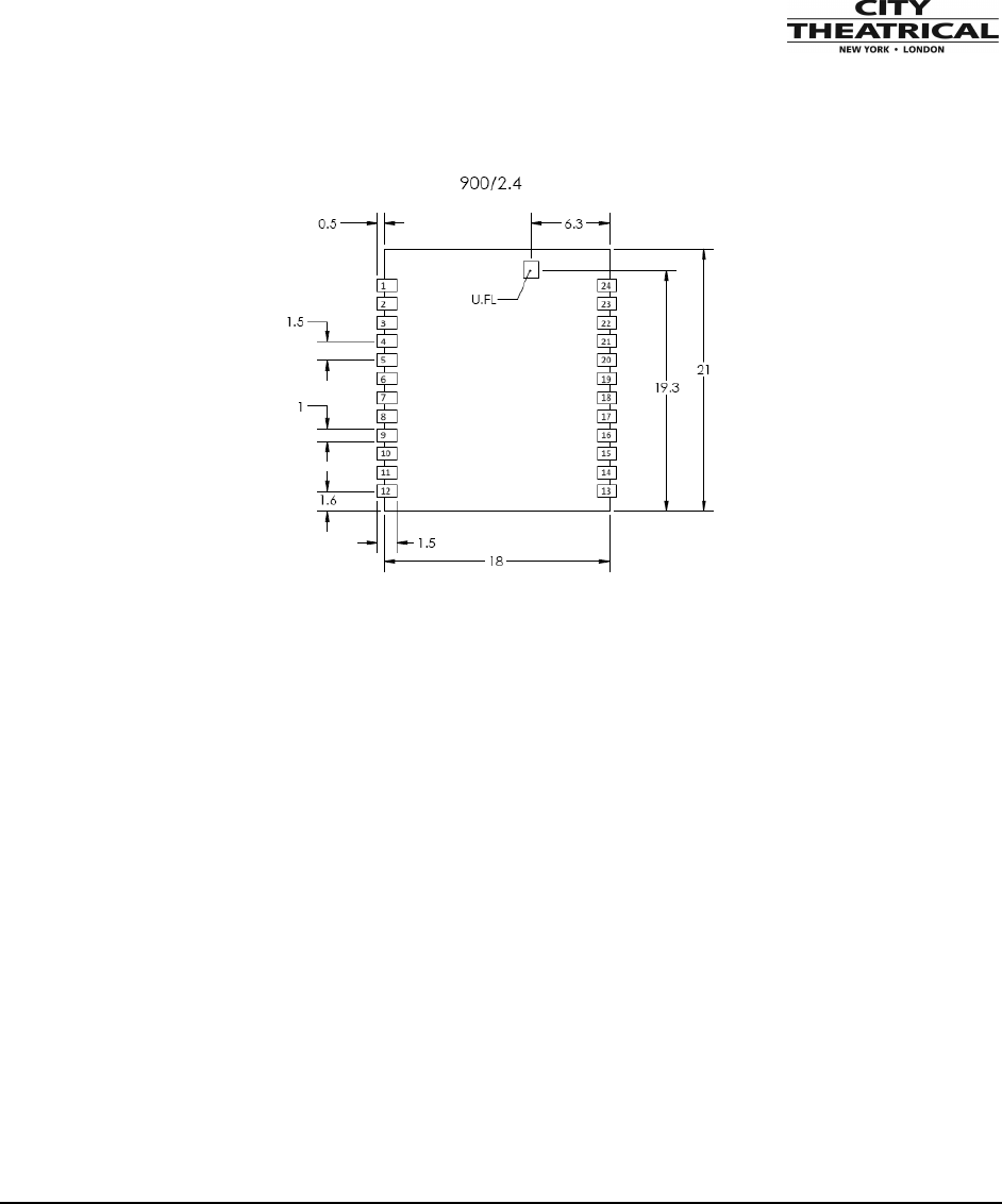
6 Signal Pinout
Table 13: Pinout Descriptions
Pin
Type
Signal Name
Function
Notes
1
GND
GND
Signal Ground
2
VCC
VCC
+3V3DC Module Power
3
VCC
VCC
+3V3DC Module Power
4
GND
GND
Signal Ground
5
I/O
JTAG_TMS
JTAG Test Mode Select
6
I
JTAG_TCK
JTAG Clock
7
I
nRESET
Module Hard Reset
Active Low
8
GND
GND
Signal Ground
9
O
UART_TXE
DMX Driver Transmit enable
10
I
UART_RX
Receive Data from DMX driver
11
O
UART_TX
Transmit Data to DMX driver
12
GND
GND
Signal Ground
13
GND
GND
Signal Ground
14
I
I2C_SCL
I2C Clock
Open-drain, 2KΩ internal pull-up
15
I/O
I2C_SDA
I2C Data
Open-drain, 2KΩ internal pull-up
16
O
I2C_nATTN
I2C Attention
Active Low
17
GND
GND
Signal Ground
18
I
SPI_nSS
SPI Slave Select
Active Low
19
I
SPI_MOSI
SPI Master output, slave input
20
O
SPI_MISO
SPI Master input, slave output
21
I
SPI_CLK
SPI Clock
Idle Low, Sample on Falling Edge
22
O
SPI_nATTN
SPI Attention
Active Low
23
GND
GND
Signal Ground
24
GND
GND
Signal Ground

599x Series
www.citytheatrical.com
18
7 OEM Interfaces
The module has three interfaces to OEM systems, SPI, I2C and DMX TTL. Not all interfaces are
required to be connected to the OEM CPU. In this section, each interface will be described
followed by the three implementation examples.
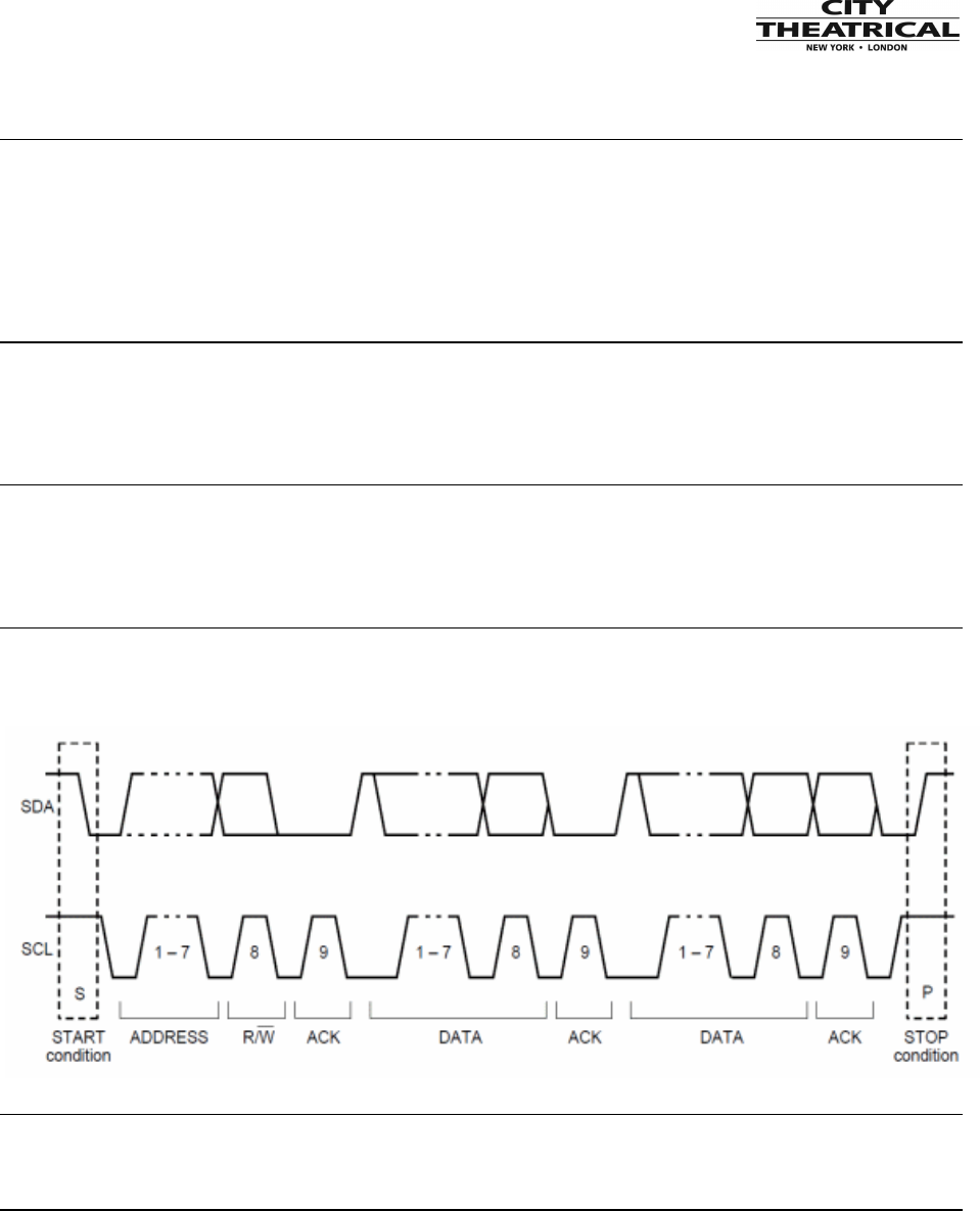
7.1 I2C
The I2C bus provides bidirectional data transfer through a 2-wire interface, a serial data line
(SDA), and a serial clock line (SCL). An Attention line is included that is active low to notify the
OEM CPU that data is available to be read. The SDA and SCL lines each have 2KΩ internal
pull-up resistors. Additional pull up resistors may be needed depending on OEM’s circuit board
design.
Do not apply a 5 volt logic signal to the I2C bus.
You can have a maximum of one module on each I2C bus. Other I2C devices are allowed on
the same buss, but may impact performance and should be evaluated.
The Multiverse I2C chip address is 0x43.
The I2C interface can operate up to fast mode (400 Kbps).
The I2C interface is the only interface for configuring the module. All configurable parameters
are read or written to this interface.
Access any to all slot data can be obtained thru this interface. Care should be taken to not
attempt to retrieve more slot data than the interface speed can support for the DMX refresh rate
currently being transmitted if loss of data is intolerable.
For devices that wish to have a single RDM presence for the integrated device, RDM messages
addressed to the OEM’s UID will come from this interface.
Addressing registers is accomplished by supplying a 2 byte address after the I2C address. The
register addresses are defined below in Table 14.
Table 14: I2C Addresses
ADDRESS
(HEX)
DESCRIPTION
# BYTES
READ/WRITE
0x0000
Product Name Length (Auto-increment on Read)
1
Read
0x0001
Product Name (String)
<= 255
Read
0x0002
Manufacturer Name Length (Auto-increment on Read)
1
Read
0x0003
Manufacturer Name (String)
<= 255
Read
0x0004
Serial Number Length (Auto-increment on Read)
1
Read
0x0005
Serial Number (String)
<= 255
Read
0x0006
Hardware Revision Length (Auto-increment on Read)
1
Read
0x0007
Hardware Revision (String)
<= 255
Read

599x Series
www.citytheatrical.com
19
0x0008
Software Revision Length (Auto-increment on Read)
1
Read
0x0009
Software Revision (String)
<= 255
Read
0x000A
Software Build Info Length (Auto-increment on Read)
1
Read
0x000B
Software Build Info (String)
<= 255
Read
0x0010
Manufacturer ID
2
Read
0x0011
Product ID
2
Read
0x0012
RDM UID
6
Read/Write
0x0013
0x0014
Hardware Binary Revision
2
Read
0x0015
Software Binary Revision
4
Read
0x0018
Operating Mode (0 = Off, 1 = Node, 2 = Hub, 0xff = Not Ready)
1
Read/Write
0x0019
Antenna Mode (0 = Auto, 1 = PCB, 2 = External)
1
Read/Write
0x001A
Modulation (xMbps)
1
Read/Write
0x001B
Modulation Minimum
1
Read
0x001C
Modulation Maximum
1
Read
0x001D
Hop Mode
1
Read/Write
0x001E
Hop Mode Minimum
1
Read
0x001F
Hop Mode Maximum
1
Read
0x0020
Hop Sub Mode
1
Read/Write
0x0021
Hop Sub Mode Minimum
1
Read
0x0022
Hop Sub Mode Maximum
1
Read
0x0023
Number of Hop Channels
1
Read
0x0024
Hop Sequence
1
Read/Write
0x0025
Hop Sequence Minimum
1
Read
0x0026
Hop Sequence Maximum
1
Read
0x0027
Transmit Power
2
Read/Write
0x0028
Transmit Power Minimum
2
Read
0x0029
Transmit Power Maximum
2
Read
0x002A
Transmit Power Code
2
Read
0x002B
Cluster ID
2
Read/Write
0x002C
RF Encoding (0 = Direct, 2 = Cross Packet)
1
Read/Write
0x002D
RF Encoding Minimum
1
Read
0x002E
RF Encoding Maximum
1
Read
0x002F
Front End Bypass (2.4GHz only)
1
Read/Write
0x0030
Receiver Status
1
Read
0x0031
Receiver RSSI
1
Read
0x0032
Clear Stats
1
Write
0x0033
Transmitter Total Packet Count
4
Read
0x0034
Receiver Total Packet Count
4
Read
0x0035
Receiver Good Packet Count
4
Read
0x0036
Receiver Repaired Packets
4
Read
0x0037
Receiver Bad Packets
4
Read
0x0038
Receiver Missed Packets
4
Read
0x0039
Max Packet Size
2
Read/Write
0x003A
Max Packet Size Minimum
2
Read
0x003B
Max Packet Size Maximum
2
Read
0x003C
Hop Period
4
Read
0x003D
FEC Sub-Blocks
1
Read/Write
0x003E
Debug Terminal Enable
1
Read/Write
0x0040
Slot Count (Size of supported slot-array)
2
Read
0x0041
Slot Interface (0 = None, 1 = SPI, 2 = DMX In, 3 = DMX Out)
1
Read/Write
0x0042
DMX Stream
1
Read/Write
599x Series
www.citytheatrical.com
20
0x0043
DMX Length
2
Read/Write
0x0044
DMX Present
1
Read
0x0046
I2C Attention
8
Read
0x0047
RDM Proxy Traffic Enable
1
Read/Write
0x0048
RDM External Parser
1
Read/Write
0x0049
RDM Response
237
Write
0x004A
RDM PD
231
Read
0x4000 –
0x49FF
DMX Slot Array, address auto-increments
1
Read/Write
7.1.1 I2C Accessible Data
The I2C Interface supports access to the types of data in Table 15.
Table 15: I2C Accessible Data
Type
Comments
Slot Data
Any slot data from any stream being sent over the wireless/wired link
RDM
RDM messages that are directed to the OEM CPU
Configuration
Configuration registers
ASC data for a universe is stored in a different stream than the universe that it was received on.
See ???? for more information on streams.
7.1.2 I2C Protocol
7.1.2.1 Strings
Strings use 2 registers. The first contains the 1-byte length (0-255) of the string while the
second contains the string itself. When the length register is read the register address auto-
increments to the string address which means if reading continues the string will clock out after
the length. Note that the auto-increment behavior only applies from the length address to the
string address. Once the string address is read the address remains at the string address and a
subsequent read will clock out the string again.
7.1.2.2 Termination and Overrun
If reading attempts to continue beyond the length of a register zeros will be clocked out
indefinitely. Zero will also provide an automatic termination for strings.
If writing continues beyond the length of a register then extra bytes are discarded.
If writing is terminated by a Stop condition before the specified number of bytes have been
written then the entire operation is discarded. A write may be suspended and re-commenced by
a repeat-Start, but this is not a common use-case.
599x Series
www.citytheatrical.com
21
7.1.2.3 Repeated Reads
The read/write logic is reset by an I2C Stop condition. Following a Stop a repeated read with no
register address write will read the same register again, except in special cases where the
register address auto-increments (string-length registers and slot array). If a read occurs with
no intervening Stop (repeated Start condition) then reading continues from the previous
position.
7.1.2.4 Repeated Writes
Following a Stop condition, the first two bytes written are always interpreted as a register
address. If a write operation begins with a repeated Start condition then it will continue from the
previous position.
7.1.2.5 Slot Array
Registers 0x4000 through 0x49FF are individual 1 byte registers at consecutive addresses.
Address auto-increments on read or write. Slots are readable in both hub and node modes.
Slots are only writeable in hub mode.
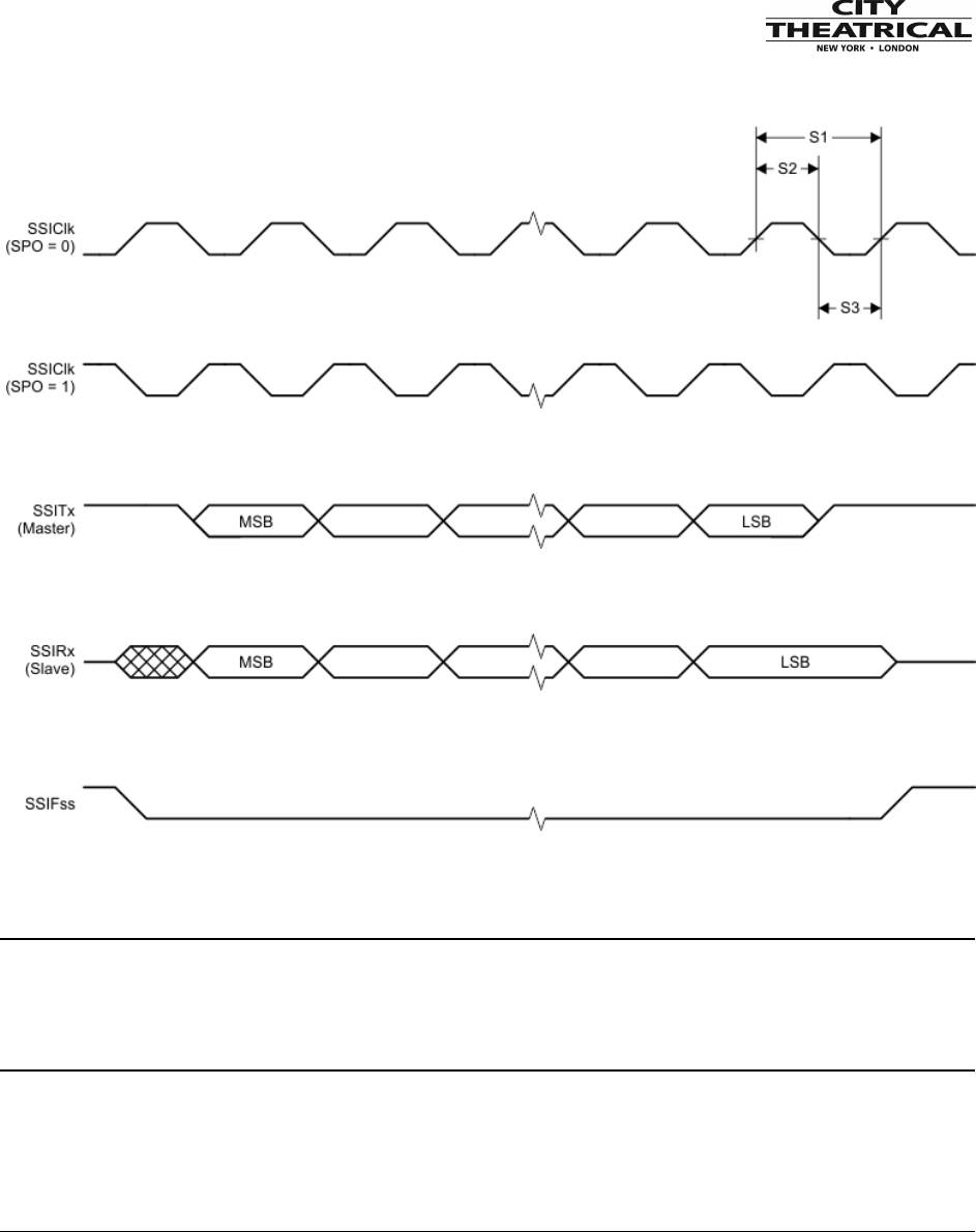
7.1.2.6 Timing diagrams
Figure 9: I2C Specification
7.1.3 I2C Register Descriptions
7.1.3.1 (0x0046) I2C Attention Register
Whenever the radio module needs to read/write data from/to the OEM CPU, it will assert the I2C
Attention line.
The OEM CPU will read this register to determine the attention reason. Reason codes are
defined in Table 17. When reading this register, there will be eight bytes returned. The first byte
is the reason, followed by 7 bytes of data. Table 16 defines the data bytes returned.
599x Series
www.citytheatrical.com
22
After reading the I2C Attention register, a read of the RDM PD register is required to get the
message data. If the PD length reported in the I2C Attention register is less 2 bytes or less, the
needed data for the RDM command will be included in the attention register and a read of the
RDM PD register is not necessary.
Table 16: I2C Attention Data Bytes
Byte
Definition
0
Attention Reason Code
1
Length of data in RDM PD register (0 – 230 bytes)
2-3
RDM PID in network byte order
4-5
RDM Sub-device number in network byte order
6-7
First 2 bytes of PD if length of PD <= 2, else random value
Table 17: I2C Attention Reason Codes
Code
Reason
0x00
Null
0x01
RDM Get message received
0x02
RDM Set message received
0x03
RDM Set Broadcast message received
0x04
Slot Value Change
7.1.3.2 (0x0047) I2C RDM Proxy Traffic Enable
7.1.3.3 (0x0049) I2C RDM Response
This write only register is used to send RDM responses back to the radio module.
The radio module will generate an ACK_TIMER with a value of 1 in the case where the OEM
CPU does not answer the RDM message within the RDM timing requirements. In order to avoid
the ACK_TIMER, the OEM CPU needs to have the complete response transferred back to the
radio module within 2ms.
When the ACK_TIMER expires and the RDM controller tries to retrieve the response and the
OEM CPU still has not supplied the response, the radio module will respond with a NACK
NR_BUFFER_FULL and consider the message cycle complete.
If the RDM controller sends a message other than Get:QUEUED_MESSAGE before or after the
ACK_TIMER and the OEM CPU writes a new response to the RDM Response register, the old
message is overwritten.
Table 18: I2C RDM Response Data Bytes
Byte
Definition
0
Length of the response message
1
RDM Response type as defined in E1.20
599x Series
www.citytheatrical.com
23
2-3
RDM PID in network byte order
4-5
Sub-Device number in network byte order
6-236
RDM PD
7.1.3.4 (0x004A) I2C RDM PD
The read only register contains the RDM PD of the message received when the PDL of the
message is greater than 2 bytes.
When the I2C Attention register is read and the PD byte is greater than 2, this register must be
read to get the RDM messages payload.
7.2 SPI
The SPI interface is used for slot data and RDM messages external to the OEM product.
The interface has an attention signal to notify the OEM CPU that the interface has data
available to be read.
This interface is mutually exclusive with the UART interface. If you use the UART for a DMX
interface, SPI is disabled. If you enable the SPI interface, the UART is disabled.
7.2.1 SPI Protocol
Table 19: Synchronous Serial Interface (SSI) Characteristics
PARAMETER NO.
PARAMETER
MIN
TYP
MAX
UNIT
S1
tclk_per SSIClk cycle time
12
????
system clocks
S2
tclk_high SSIClk high time
0.5
tclk_per
S3
tclk_low SSIClk low time
0.5
tclk_per
Figure 10: SSI Timing
599x Series
www.citytheatrical.com
24
7.3 UART
The UART interface is used to handle a single universe of DMX/RDM data. It is capable of
proxying a limited number of RDM devices.
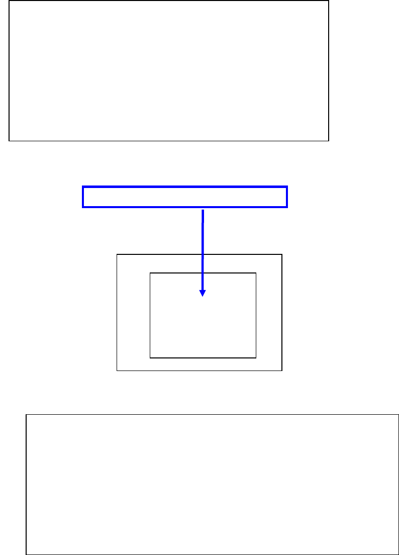
7.4 Recommended Configurations
The interfaces that are connected to the OEM CPU should fall into one of three setups. These
setups are based on what your data needs are and whether you intend to appear as a unified
RDM device or not.
7.4.1 Minimal
This configuration has the following features:
DMX is not intended to be sent from module
Consumed DMX slots are retrieved via the I2C interface
All configuration operations set via I2C interface
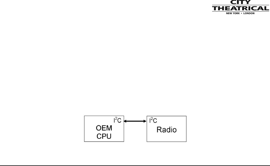
599x Series
www.citytheatrical.com
25
OEM CPU stores and sets configuration data
OEM provides user interface
OEM CPU answers unicast RDM messages thru I2C interface
Your device will show as one RDM devices
In this configuration, the OEM only needs to supply power and provide an I2C interface
connection.
Figure 11: Minimal Configuration Block Diagram
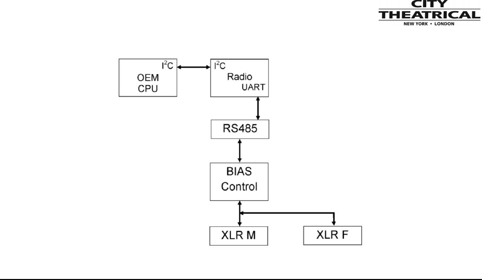
7.4.2 Basic
This configuration has the following features:
One universe of DMX/RDM is handled by the module
o Can receive wired DMX/RDM (Does not transmit wirelessly)
o Can send wirelessly received DMX/RDM
Consumed DMX slots can be retrieved via the I2C interface
o In both wired and wireless directions
All configuration operations are set via I2C interface
OEM stores and sets configuration data
OEM provides user interface
OEM answers unicast RDM messages thru I2C interface
OEM device will show as one RDM devices
Can proxy up to 50 end devices on DMX/RDM UART interface
In this configuration, the OEM supplies power and connects to the I2C interface. The UART
interface is connected to a DMX driver and associated RDM line bias network.
Figure 12: Basic Configuration Block Diagram
599x Series
www.citytheatrical.com
26
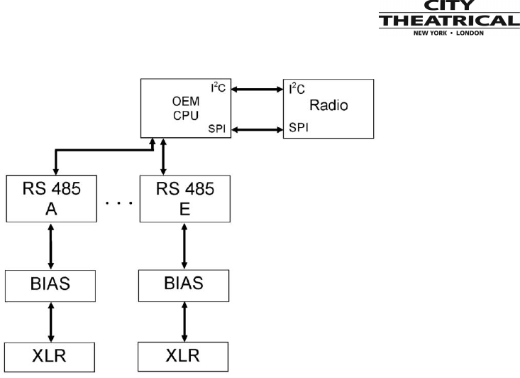
7.4.3 Advanced
This configuration has the following features:
All configuration operations are set via I2C interface
OEM stores and sets configuration data
OEM provides user interface
OEM device will show as one RDM devices
Up to 5 universes of slot data is accessed thru the SPI interface
Proxied RDM messages are handled thru the SPI interface
OEM is responsible for generating DMX/RDM ports, if required
OEM is responsible for providing RDM proxy services
OEM maintains the RDM proxy list
In this configuration, the OEM supplies power and connects to the SPI and I2C interfaces. If the
design requires DMX/RDM ports on the product, the OEM has to generate those ports from the
SPI data and provide RDM proxy services.
Figure 13: Advanced Configuration Block Diagram
599x Series
www.citytheatrical.com
27

599x Series
www.citytheatrical.com
28
8 Tape and Reel Information

599x Series
www.citytheatrical.com
29
9 Reflow Profile
Information and graph for reflow profile