Users Manual

1
Users Manual
Model No. : HJZ0095 and HJZ0093
FCC ID : SJ2HJZ0095
IC ID : 5427A HJZ0095
Xanavi Informatics Corporation

2
List of content
1. General information
- Name of product
- Model Name
- Descriptions
2. Procedure to build in
2.1 Procedure for HJZ0095
2.2 Procedure for HJZ0093
3. Pin Description of Connector
4. Label Information
4.1 HJZ0095
4.2 HJZ0093
5. Caution
6. Regulatory information
7. Product information
3
1. General information
- Name of product
Bluetooth Module
- Model Name
Manufacture name
Xanavi Informatics Corporation Sony Corporation Difference of product
HJZ0093 (*1) CXN1041-3AAC
- Output PCM clock signals
included Synch clock as
master mode from the module
- 921.6kbps in UART Baud rate
HJZ0095 (*2) CXN1041-3ABC
- Input PCM clock signals
included Synch clock as slave
mode to the module
- 115.2kbps in UART Baud rate
(*1) Based on HJZ0093, fully compatible with the CXN1041-3AAC from SONY
(*2) Based on HJZ0095, fully compatible with the CXN1041-3ABC from SONY
Note 1 : There is no hardware change between above two models.
Note 2 : The IC,CXD 3264, used these Module has its own power supply regulator.
- Descriptions
The HJZ0093 and HJZ0095 are a fully integrated Class 2 Radio and baseband module conforming to
ver.1.2 of the Bluetooth Core specification.
4
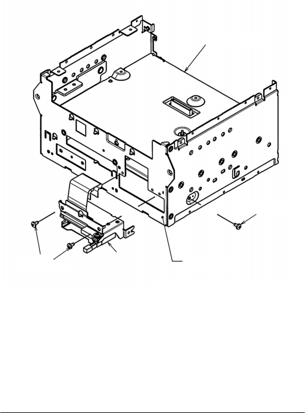
2. Procedure to build in:
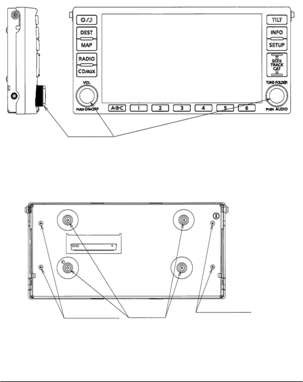
2.1 Procedure for HJZ0095
A mounting position of the Bluetooth module
Volume knobs 1) Pulling out volume knobs
Two screws Four screws Two screws
2) Removing two types and
eight screws
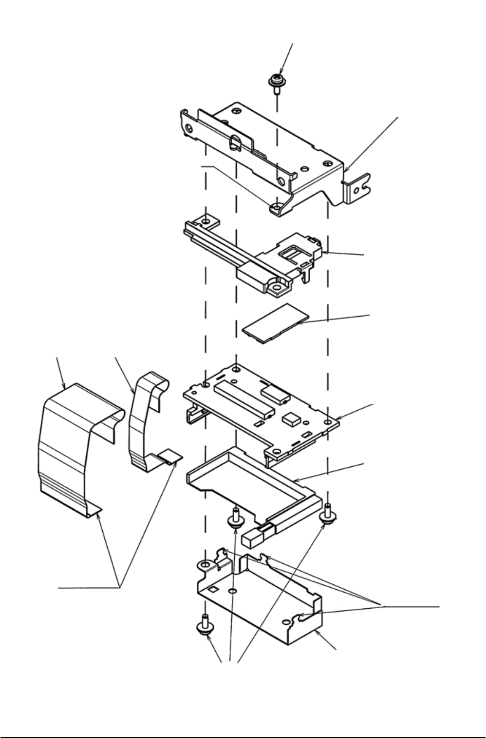
5
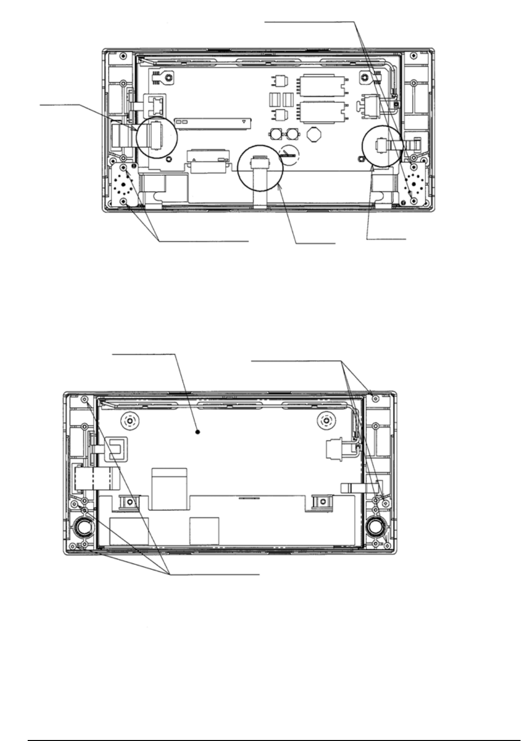
Two screws
Two screws FPC cables with connectors
FPC cables with
connectors
3) Removing four screws and pulling out
FPC cable from the connectors
Three screws
Three screws
4) Removing six screws
6
2. Bluetooth
SW printed wiring
board R SW printed wiring
board L SW printed wiring
board R
5) Removing the Bluetooth module
from SW pwb R
7
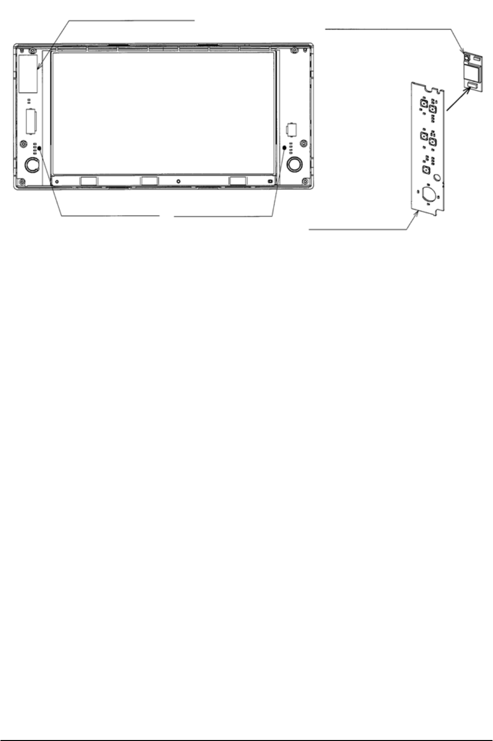
2.2 Procedure for HJZ0093
A mounting position of the Bluetooth module
Navigation Unit
Two screws
A
screw
Front cover
1) Removing three screws and pulling out
FPC cable from the connectors
8
A
screw
A
screw
Bluetooth module
CF bracket
CF Bluetooth cover
CF & HDD pwb
CF ejector
Bottom is
contact side
CF shield cover
Clinches
FPC-15pin
FPC-35pin
2) Removing four screws and pulling
out FPC cable from the connectors
9
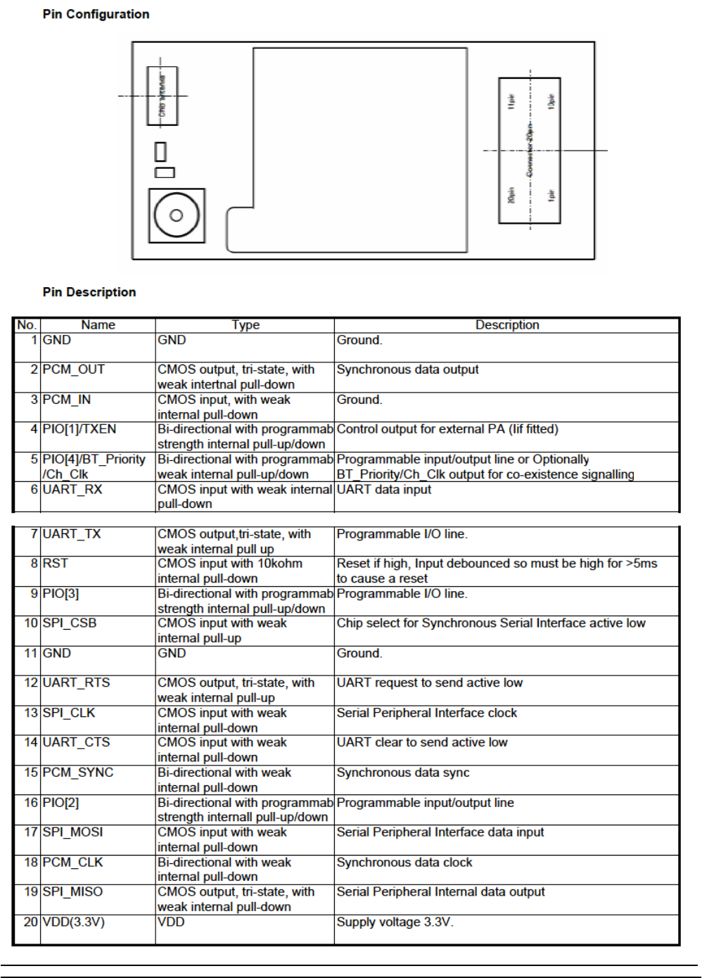
3. Pin Description of Connector
10
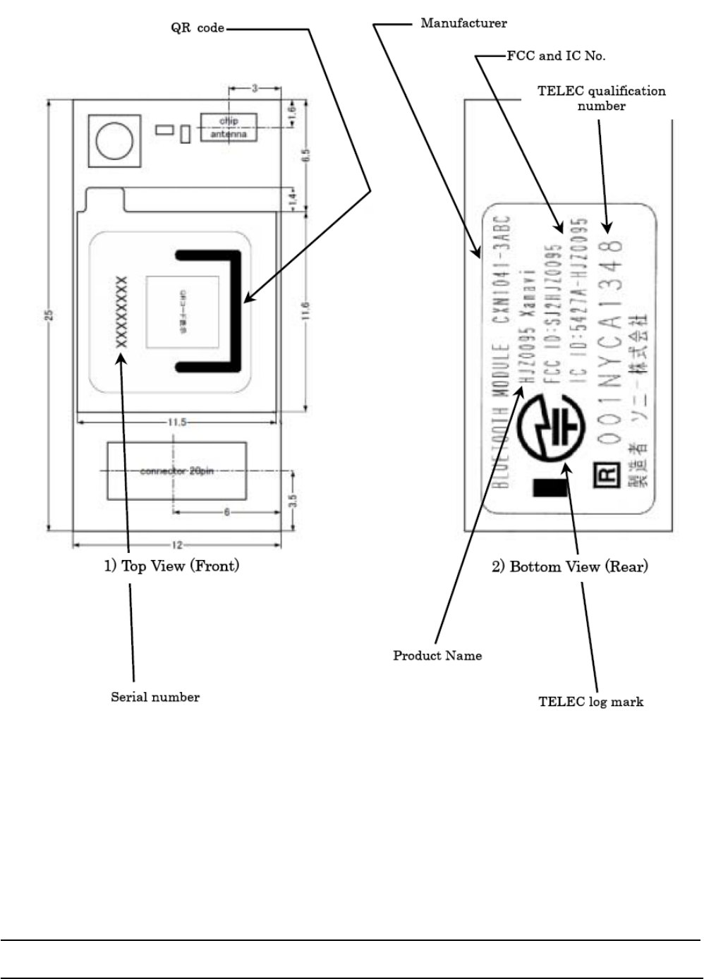
4. Label Information
4.1 HJZ0095
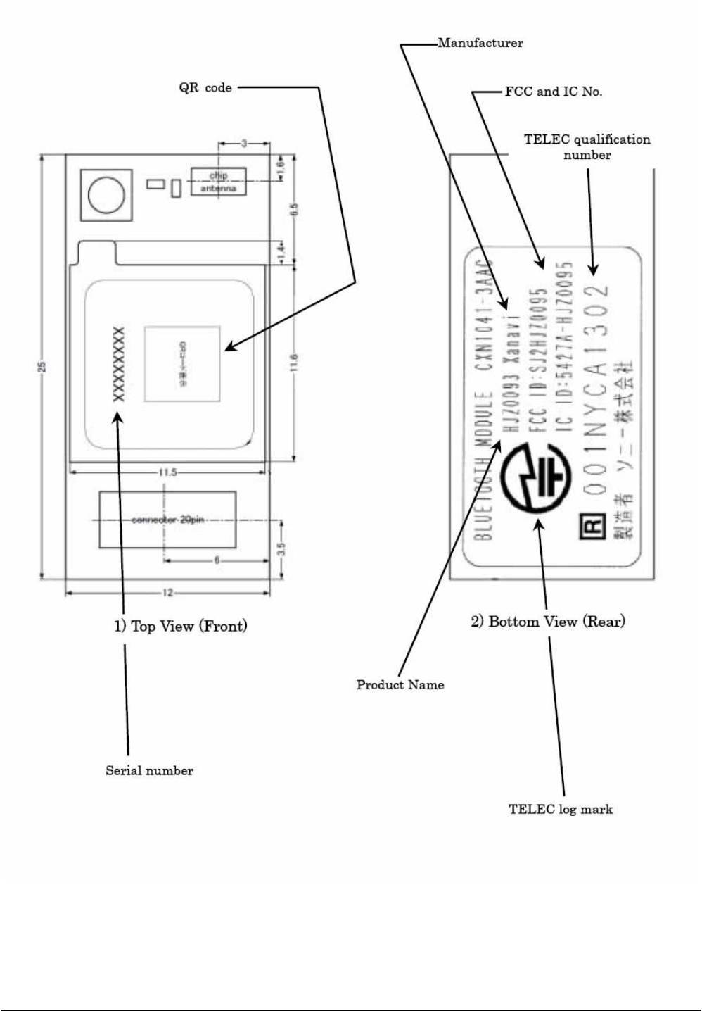
11
4.2 HJZ0093

12
5. Caution
- The following sentence has to be displayed on the outside of the device in which the module is
installed: "Contains Transmitter Module FCC ID: SJ2HJZ0095", or "Contains FCC ID:
SJ2HJZ0095".
- Please note that this users manual should not be provided to end-users.
- In the User manual or Label of the device (end-set), which install HJZ0095 or HJZ0093, following
Regulatory information should be mentioned.
6. Regulatory information
FCC Regulatory information
- CAUTION: To maintain compliance with FCC’s RF exposure guidelines, use only the supplied
antenna. Unauthorized antenna, modification, or attachments could damage the transmitter and may
violate FCC regulations.
- Operation is subject to the following two conditions:
1) this device may not cause interference and
2) this device must accept any interference, including interference that may cause undesired
operation of the device
IC Regulatory information
- Operation is subject to the following two conditions: (1) this device may not cause interference, and
(2) this device must accept any interference, including interference that may cause undesired
operation of the device.
L'utilisation de ce dispositif est autorisee seulement aux conditions suivantes : (1) il ne doit pas
produire de brouillage et (2) l'utilisateur du dispositif doit etre pret a accepter tout brouillage
radioelectrique recu, meme si ce brouillage est susceptible de compromettre le fonctionnement du
dispositif.
- This Class B digital apparatus meets all requirements of the Canadian Interference-Causing
Equipment Regulations.

13
7. Product information
頁
7.1. 製品仕様..................................................................................................................................14
7.1. 製品概要 ...............................................................................................................................14
7.2. 電気的特性 ...........................................................................................................................16
7.3. FIRMWARE............................................................................................................................18
添付資料 1 使用部品 12
14
7.1. 製品仕様
7.1. 製品概要
CXN1041 はBluetooth Specification Ver.1.2 Class2 の認証を取得した、Bluetooth 用RF/ベースバン
ドフルモジュール
7.1.1. 特長
・UART,PCM CODEC,PIO のインターフェースに対応
・パッケージサイズ:12×25×2.55 [mm]
・内蔵 FLASH MEMORY 容量は 8M Bit
・アンテナ搭載
・CXD3264GL は、CSR 社の BlueCore4-EXT と完全コンパチブル
・1つのマスタから 7スレーブまで対応
・チャネル品質駆動データレート
一般仕様
・品名 Bluetooth モジュール
・型番 CXN1041-3AAC、CXN1041-3ABC
・外部 IF UART(BCSP BAUD RATE 921.6kbaud)、PCM、PIO
・電源電圧 2.7∼3.6 [V]
・外形寸法 12×25×2.55 [mm]
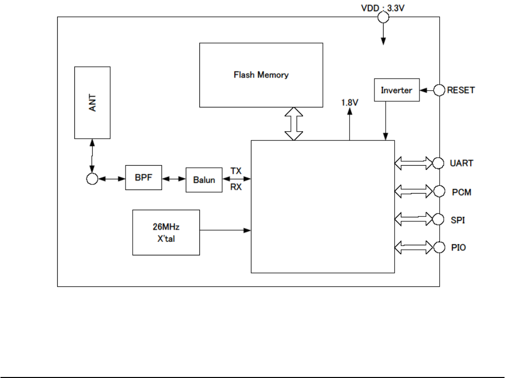
7.1.2. ブロック図
CXD3264GL
15
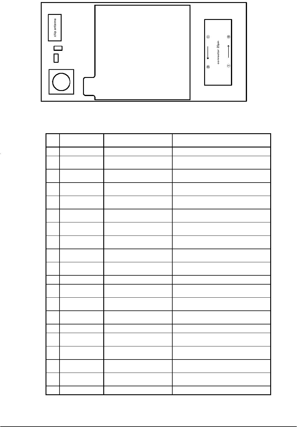
7.1.3. 端子配列
端子説明
端子
番号
端子記号 タイプ 端子説明
1GND
GND グランド
2PCM_OUT
CMOS出力、内部弱プルダウン
付きでトライステート可能 PCMデータ出力
3PCM_IN
CMOS入力、内部弱プルダウン
付き PCMデータ入力
4PIO[1]
双方向、プログラマブル、内部強
プルアップ/ダウン付き プログラマブル入出力ライン
5PIO[4]
双方向、プログラマブル、内部強
プルアップ/ダウン付き プログラマブル入出力ライン
6UART_RX
CMOS入力、内部弱プルダウン
付き UARTデータ入力
7 UART_TX
CMOS出力、内部弱プルアップ
付きでトライステート可能 UARTデータ出力
8RST
CMOS入力 High時リセット。入力がデバウンスされるので、リセットにするため
に5ms以上Highにして下さい。
9PIO[3]
双方向、プログラマブル、内部強
プルアップ/ダウン付き プログラマブル入出力ライン
10 SPI_CSB
CMOS入力、内部弱プルアップ
付き Synchronous Serial Interface用チップ選択、
アクティブLow
11 GND
GND グランド
12 UART_RTS
CMOS出力、内部弱プルアップ
付きでトライステート可能 UART送信リクエスト、アクティブLow
13 SPI_CLK
CMOS入力、内部弱プルダウン
付き Serial Peripheral Interfaceクロック
14 UART_CTS
CMOS入力、内部弱プルダウン
付き UART送信クリア、アクティブLow
15 PCM_SYNC
双方向、内部弱プルダウン PCMデータ同期
16 PIO[2]
双方向、プログラマブル、内部強
プルアップ/ダウン付き プログラマブル入出力ライン
17 SPI_MOSI
CMOS入力、内部弱プルダウン
付き Serial Peripheral Interfaceデータ入力
18 PCM_CLK
双方向、内部弱プルダウン付き PCMデータクロック
19 SPI_MISO
CMOS出力、内部弱プルダウン
付きでトライステート可能 Serial Peripheral Interfaceデータ出力
20 VDD
VDD 電源電圧
16
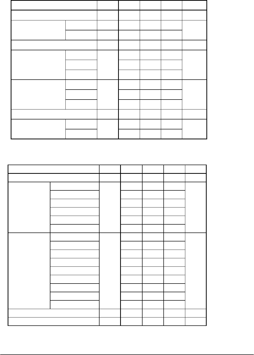
7.2. 電気的特性
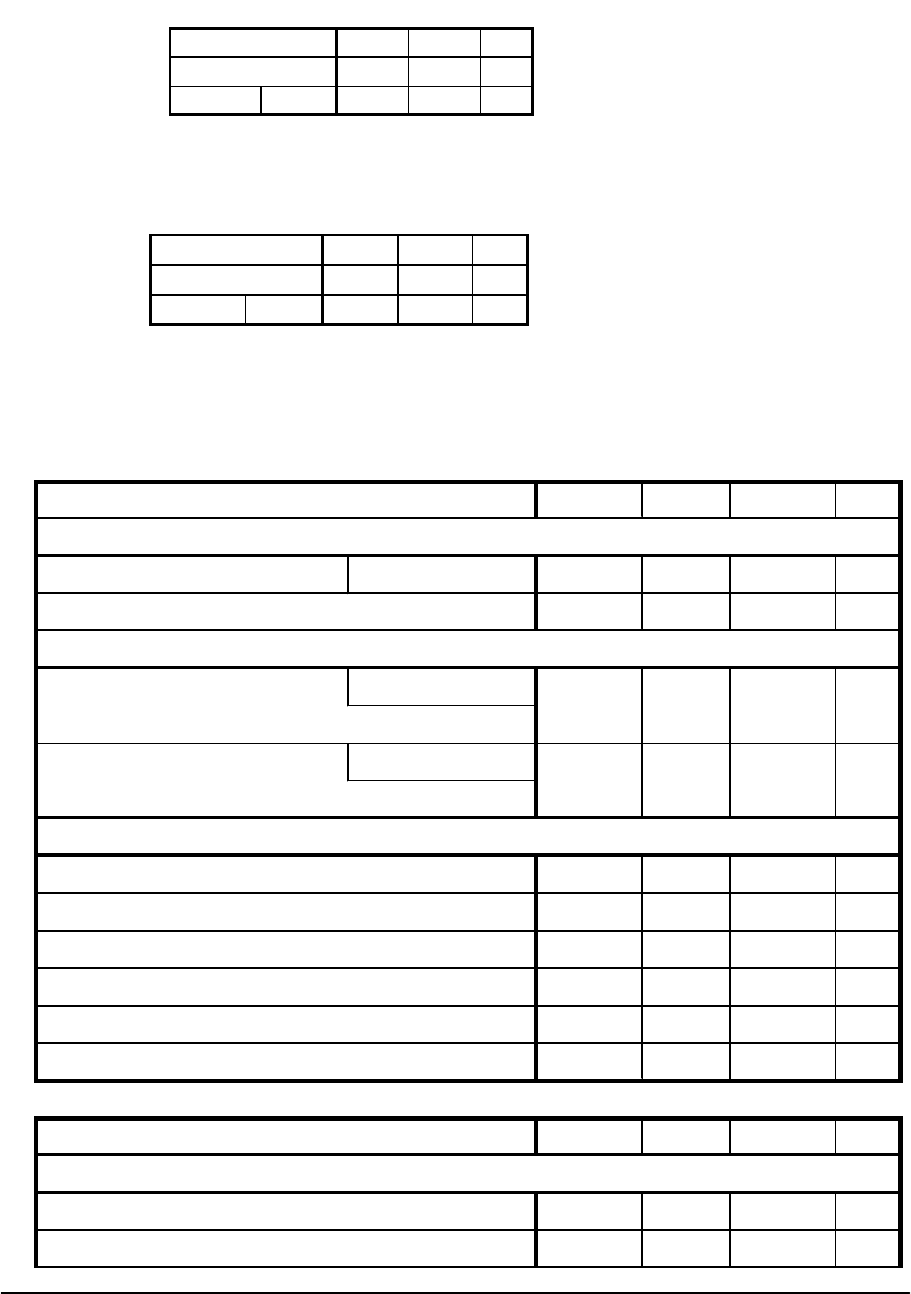
7.2.1. 絶対最大定格
最小値 最大値 単位
-40 85 ℃
電源電圧 VDD -0.40 3.60 V
項目
保存温度範囲
7.2.2. 推奨動作条件
最小値 最大値 単位
-40 85 ℃
電源電圧 VDD 2.70 3.60 V
項目
動作温度範囲
7.2.3. 入力/出力端子特性
(Ta:-40∼+85℃)
※本端子特性は、CXN1041 の内部で使用している CXD3264GL の仕様です。
最小値 標準値 最大値 単位
V
IL
入力ロジックレベルLow 2.7≦VDD≦3.6V -0.4 +0.8 V
0.7VDD VDD+0.4 V
V
OL
出力ロジックレベルLow 2.7≦VDD≦3.6V
VOL出力ロジックレベルHigh 2.7≦VDD≦3.6V
-100 -40 -10 μA
+10 +40 +100 μA
-5.0 -1.0 -0.2 μA
+0.2 +1.0 +5.0 μA
-1 0 +1 μA
1.0 5.0 pF
最小値 標準値 最大値 単位
入力ロジックレベルLow -0.4 0.2VDD V
入力ロジックレベルHigh 0.8VDD VDD+0.4 V
RST端子
入力電圧
(I
O
=-4.0mA)
入力/トライステート電流
強プルアップ
強プルダウン
VVDD-0.2
C
I
入力容量
入出力パッドリーク電流
弱プルダウン
弱プルアップ
V
IH
入力ロジックレベルHigh
出力電圧
(I
O
=4.0mA)
デジタル端子
入力電圧
V0.2
17
7.2.4. 高周波特性
条件 最小値 標準値 最大値 単位
N&ETC -6 0 4 dBm
⊿f1avg N&ETC 140 165 175
⊿f2max N&ETC 115 160
N&ETC 10 75 kHz
DH1 5 25
DH3 10 40
DH5 10 40
DH1 5 20
DH3 10 20
DH5 10 20
N&ETC 915 1000 kHz
¦M-N¦=2 -40 -20
¦M-N¦≧3 -50 -40
NTC:Normal Test Conditions +15∼+35℃、ETC:Extreme Test Conditions -40∼+85℃
送信
kHz
kHz
kHz/50μs
出力電力(平均)
dBmN&ETC
20dB帯域幅
変調特性
キャリア周波数ドリフト
(絶対値)
ドリフトレート
(絶対値)
近接チャンネル電力
初期キャリア周波数許容差(絶対値)
N&ETC
N&ETC
条件 最小値 平均値 最大値 単位
N&ETC -84 -70 dBm
co-ch 8 11
1MHz -2 0
2MHz -34 -30
≧3MHz -43 -40
Image -18 -9
Image±1MHz -23 -20
30∼2G -10
( 824M∼849M ) 2
( 880M∼915M ) 7
( 1.71GG∼1.785G ) 6
( 1.85G ∼1.91G ) 5
( 1.92G∼1.98G ) -6
2G∼2.399G -27
2.498G∼3G -27
3G∼12.75G -27
NTC -39 -30 dBm
NTC -20 0 dBm
NTC:Normal Test Conditions +15∼+35℃、ETC:Extreme Test Conditions -40∼85℃
相互変調性能
最大入力レベル
NTCC/I性能
受信
dB
ブロッキング性能 NTC dBm
感度(シングルスロットパケット)

18
7.2.5. 消費電流
モード 平均値 単位
SCO接続HV3(30ms interval Sniff Mode) 21 mA
SCO接続HV1(マスタまたはスレーブ) 42 mA
ACLデータ転送720kbps UART(マスタまたはスレーブ) 45 mA
ACL接続、スニフモード40ms間隔、38.4kbps UART 3.2 mA
ACL接続、スニフモード1.28s間隔、38.4kbps UART 0.45 mA
Parkedスレーブ、1.28ビーコン間隔、38.4kbps UART 0.55 mA
スタンバイモード(ホスト接続、RF停止) 47.0 μA
Reset 15.0 μA
最大消費電流:100mA 以下
7.3. Firmware
Software Stack
CSR HCI Stack (Ver.19.2)

19
添付資料 1: 使用部品
使用している主要部品
品名 メーカー 備考
CXD3264GL ソニーセミコンダクター九州(株) Bluetooth IC
MBM29SL800BE90PW-J-ERE1 Spansion Japan 株式会社 Flash Memory
LDA31 村田製作所 株式会社 チップアンテナ
MM8430-2600B 村田製作所 株式会社 SW付RFコネクタ
20ピン、ボードトゥボードコネクタ
適合コネクタ:AXK5F20545Y
AXK6F20345Y 松下電工株式会社