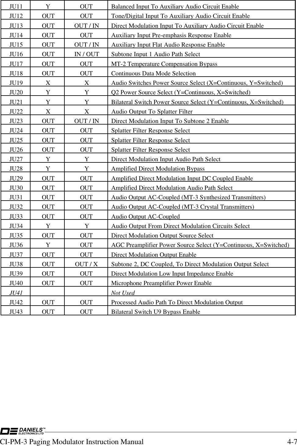
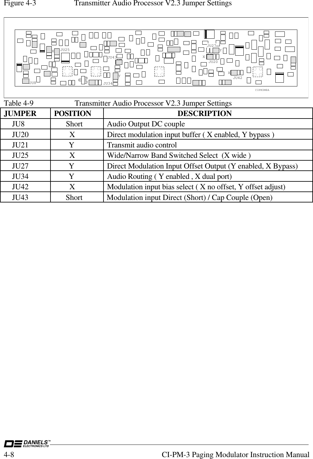
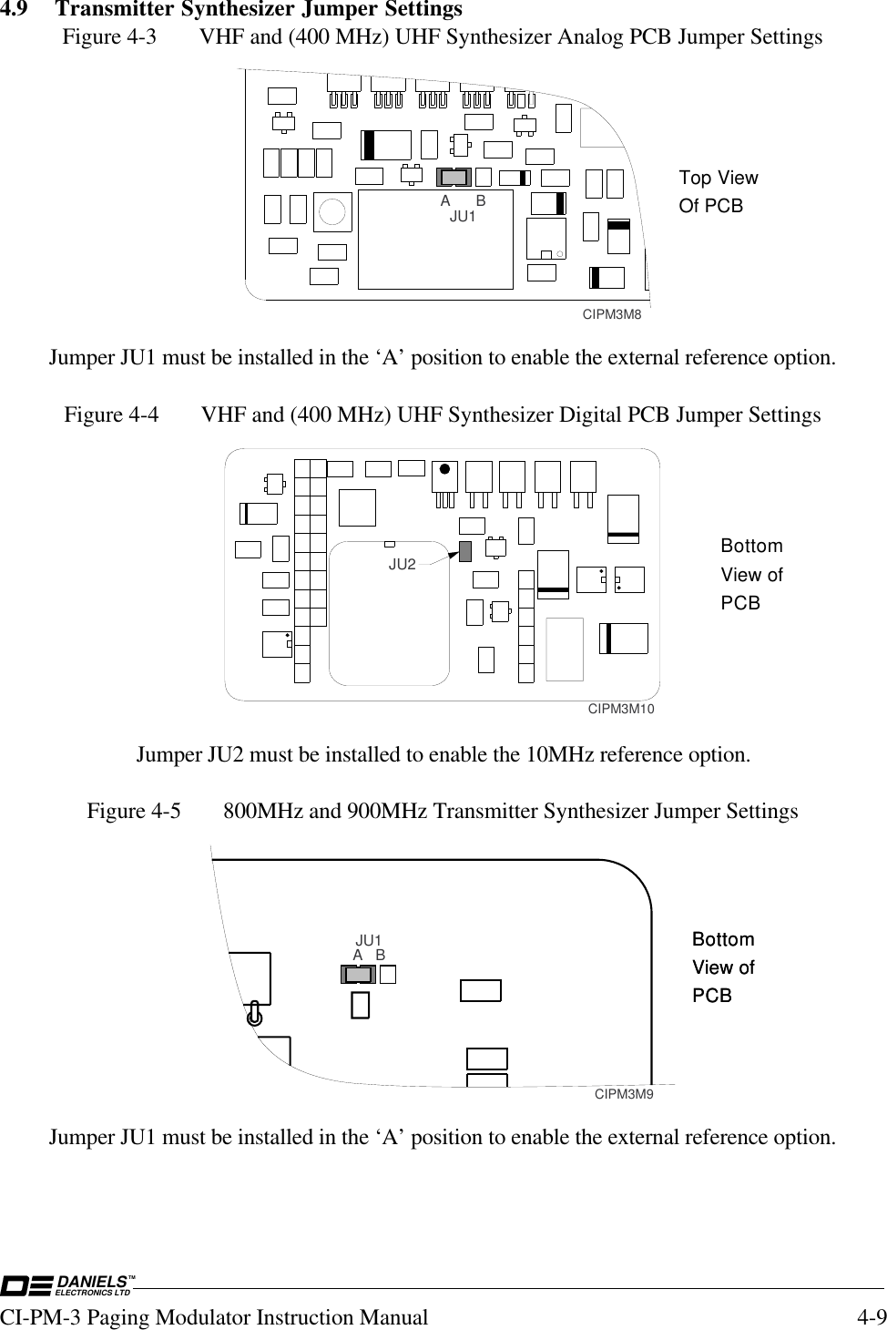
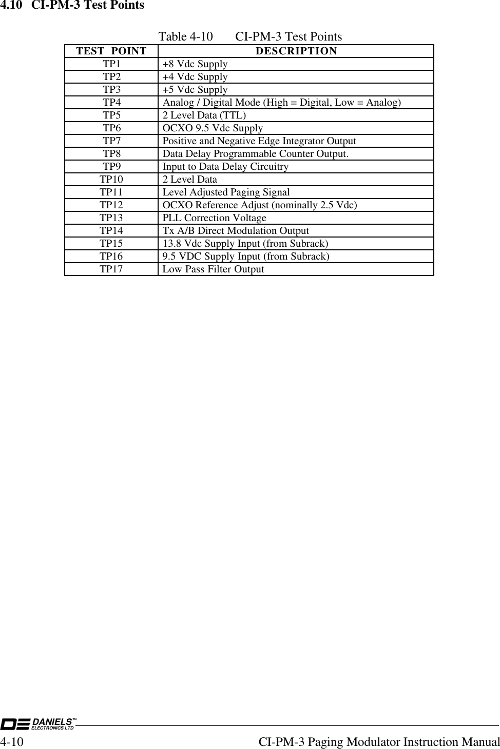
Codan Radio Communications UT-3-460-S08 UT-3-460-S Paging Transmitter User Manual IM23 UT3400 4
Codan Radio Communications UT-3-460-S Paging Transmitter IM23 UT3400 4
UserManual.wiki
>
Codan Radio Communications
>
UT-3-460-S08 User Manual
>
Users guide
Contents
1.
Users guide
2.
Revised users guide
Users guide
Navigation menu
Upload a User Manual
Namespaces
Wiki Guide
HTML
PDF
Info
Views
User Manual
Discussion / Help
Navigation


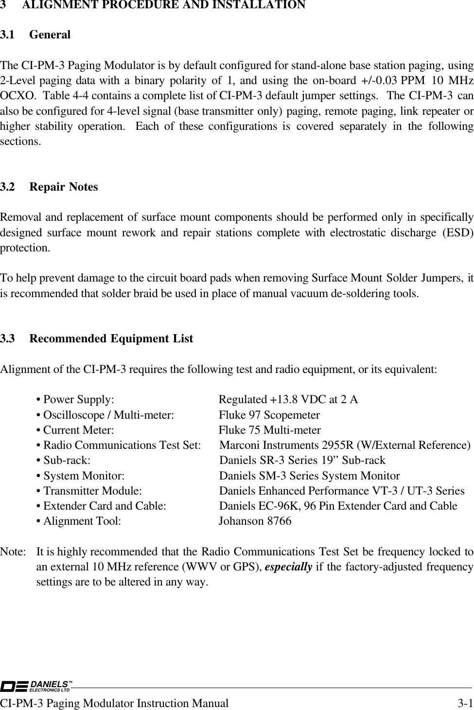


![Enhanced AM/FM Synthesizer Instruction Manual OS(R/T)-3(A/H) 29 - 470 MHz 1-31.3 Performance SpecificationsType:Narrow band FM, Single loop synthesizer module utilizing low noise VCO and PLL technology.Compatible with Daniels MT-3 series Transmitter and Receiver modules.Frequency Range:29 MHz - 38 MHz [±0.5 MHz] (OST-3H035)(Tuning range with no adjustment 38 MHz - 50 MHz [±1.0 MHz] (OST-3H045)is shown in [ ] brackets.) 50.4 MHz - 71.4 MHz [±1.0 MHz] (OSR-3H061)118 MHz -138 MHz [Full band] (OST-3A128)128 MHz - 152.6 MHz [±2.0 MHz] (OST-3H141, OSR-3H141)139.4 MHz - 159.4 MHz [Full band] (OSR-3A149)150 MHz - 174 MHz [±2.0 MHz] (OST-3H162, OSR-3H162)406 MHz - 430 MHz [Full band] (OST-3H418)427.4 MHz - 451.4 MHz [Full band] (OSR-3H440)450 MHz - 470 MHz [Full band] (OST-3H460)Output Power:+5 dBm ±2 dBm into 50ΩHarmonics:<-30 dBcSpurious:<-90 dBc<-70 dBc above 400 MHzAttack Time:<10 ms (Normal Mode)<50 ms (Low Current Standby Mode)Hum and Noise: -55 dB](https://usermanual.wiki/Codan-Radio-Communications/UT-3-460-S08.Users-guide/User-Guide-298251-Page-129.png)