Codan Radio Communications VT-3-150-SN VT-3/140-SN & VT-3/160-SN VHF TRANSMITTERS User Manual IM21 VT3150AMP VHF Tx Amplifier Manual
Codan Radio Communications VT-3/140-SN & VT-3/160-SN VHF TRANSMITTERS IM21 VT3150AMP VHF Tx Amplifier Manual
VHF Tx Manual including schematics and parts list

MT-3
RADIO
SYSTEMS
VHF TRANSMITTER
INSTRUCTION MANUAL
VT-3
132 - 174 MHz
Covers model:
VT-3/140-SWA2, VT-3/160-SWA2
VT-3/140-SWA8,
VT-3/160-SWA8
VT-3/140-SNA2,
VT-3/160-SNA2
VT-3/140-SNA8,
VT-3/160-SNA8
Copyright © 1998 Daniels
Electronics
Ltd.
All
rights
reserved.
No part of this
publication
may be
reproduced,
stored in a
retrieval
system or
transmitted
in any form or by any
means,
electronic,
mechanical,
photocopying,
recording or
otherwise,
without
the prior
written
consent of Daniels
Electronics
Ltd.
DE™ is a
registered
trademark
of Daniels
Electronics
Ltd.
registered
in the United States
Patent
and
Trademark
Office.
Issue: 3 Previous Issue: 2
Issue Date: May 1998 Previous Issue Date:
April
1997 Daniels
Electronics
Ltd.
Printing Date: January 2001
Victoria,
B.C.
Part No.: IM21-VT3150 PRINTED IN
CANADA

ii VHF
Enhanced
Transmitter
Instruction Manual VT-3 132 - 174 MHz
NOTE:
The user's
authority
to
operate
this
equipment
could be
revoked
through any
changes or
modifications
not expressly
approved
by Daniels
Electronics
Ltd.
The design of this
equipment
is subject to change due to continuous
development.
This
equipment
may
incorporate
minor changes in
detail
from the
information
contained
in this manual.

VHF
Enhanced
Transmitter
Instruction Manual VT-3 132 - 174 MHz
iii
TABLE OF CONTENTS
Page
1 GENERAL................................................................................................................. 1-1
1.1
Introduction
.................................................................................................... 1-1
1.2 Manual
Organization
...................................................................................... 1-1
1.3 VT-3 132 - 174 MHz
Transmitter
Family
Models.......................................... 1-2
1.4
Performance
Specifications
............................................................................. 1-3
1.4.1 General............................................................................................... 1-3
1.4.2 Audio
Specifications
........................................................................... 1-4
1.4.3 Physical
Specifications
....................................................................... 1-5
2
SYSTEM OVERVIEW
.............................................................................................. 2-1
2.1
Transmitter
Operation..................................................................................... 2-1
2.2 Frequency
Selection
........................................................................................ 2-3
2.2.1
Synthesizer
Transmitter
.................................................................... 2-3
2.3
Transmitter
Assembly and
Adjustment
........................................................... 2-4
2.3.1
Complete
Transmitter
Alignment
........................................................ 2-4
2.3.2 Frequency Change.............................................................................. 2-5
2.3.3 Output Power
Adjustment
................................................................... 2-5
2.3.4
Deviation
Setting
................................................................................. 2-6
2.3.5
Setting
RF
Alarm
Thresholds............................................................. 2-6
2.4
Recommended
Test
Equipment
List................................................................ 2-6
2.5 Repair Note..................................................................................................... 2-7
2.6 Printed
Circuitboard
Numbering
Convention
.................................................. 2-7
3 ILLUSTRATIONS..................................................................................................... 3-1
3.1 MT-3
Transmitter
Front Panel........................................................................ 3-1
3.2 MT-3
Transmitter
Case - Exploded
View
....................................................... 3-2
4 PARTS LIST.............................................................................................................. 4-1
5 REVISION HISTORY............................................................................................... 5-1
MODULE MANUALS
Transmitter
Main Board Instruction Manual ......................................IM20-MT3TXMN
VHF
Amplifier
Instruction Manual VT-3 132 - 174 MHz................IM21-VT3150AMP
Enhanced
Synthsizer Instruction Manual OS(R/T)-3A/H 29-470 MHz .. IM10-OS3AH
VHF
Transmitter
Channel Designation
Table
..................................... IM21-VT3150CT

RF Exposure Warning
RF Exposure Warning
This transmitting equipment conforms to SAR (Specific Absorption Rate) limits regarding exposure of human
beings to radio frequency electromagnetic energy, as defined in the following national and international standards
and guidelines:
1. Industry Canada Radio Standards Specification 102 (RSS-102), Evaluation Procedure for Mobile and
Portable Radio Transmitters with respect to Health Canada’s Safety Code 6 for Exposure of Humans to
Radio Frequency Fields;
2. Health Canada Safety Code 6, Limits of Human Exposure to Radiofrequency Electromagnetic Fields in the
Frequency Range from 3 kHz to 300 GHz1;
3. United States Federal Communications Commission, Code of Federal Regulations; 47 CFR Part 1,
§ 1.1310 Radiofrequency radiation exposure limits; and
4. American National Standards Institute (ANSI) criteria for localized SAR in Section 4.2 of “IEEE Standard
for Safety Levels with Respect to Human Exposure to Radio Frequency Electromagnetic Fields, 3 kHz to
300 GHz”2.
Notes: A. The SAR limit for uncontrolled exposure of persons not classed as RF and microwave exposed
workers (including the general public) for transmitter equipment operating below 10 GHz, as defined
in the references above, is 2 W/m2 (0.2 mW/cm2).
B. This transmitting equipment is designed for use with an outdoor antenna with a characteristic antenna
gain of 10 dBi, typically mounted at a significant height above ground to provide for adequate signal
coverage. To ensure that the general public is not exposed to a power density above the recommended
limit of 2 W/m2 (0.2 mW/cm2), the equipment must be installed such that the following minimum safe
distances from the antenna are maintained:
6.3 m (20.7 ft) when configured with 100 W PA
3.5 m (11.3 ft) when configured with 30 W PA
1.8 m (5.9 ft) standalone (i.e. no PA) 8 W
C. The following power density formula has been utilized in determining minimum safe distances:
2
4
R
P
G
S
π
=
where: S = Power density (in appropriate units, e.g. mW/cm2)
P = Power input to the Antenna (in appropriate units, e.g., mW)
G = Power gain of the antenna in the direction of interest relative to an isotropic radiator
R = Distance to the center of radiation of the antenna (appropriate units, e.g., cm)
1 Minister of Public Works and Government Services, Canada 1999, Cat. H46- 2/ 99- 237E, ISBN 0- 662- 28032- 6
2 ANSI/IEEE C95.1–1992, Copyright 1992 by the Institute of Electrical and Electronics Engineers, Inc., New York, New York 10017

VHF Enhanced Transmitter Instruction Manual VT-3 132 - 174 MHz
1-1
1
GENERAL
1.1 Introduction
The VT-3 132 - 174 MHz
Transmitter
is a low
power,
synthesized FM
transmitt
er
capable
of
operating
in 12.5 kHz or 25/30 kHz channels. The
transmitter
operates continuous duty in one of
two frequency bands: 132 to 150 MHz or 150 to 174 MHz and its output power is
continuously
adjustable
from 0.5 T0 2.0 or 2.0 to 8.0 Watts. A modular design
allows
each of the
transmitter's
modules;
MT-3
Transmitter
Board,
MT-3 Audio Processor,
VT-3/150
Amplifier,
and
OS-3H150
Synthesizer Module to be
individually
assembled and tested. This
facilitates
construction,
tuning,
maintenance
as
well
as
troubleshooting
procedures. The synthesizer module can be
programmed
to
have
up to 16 channels
exclusive
to one frequency band.
The VT-3 132 - 174 MHz
Transmitter
is designed to
interface
with
Daniels
Electronics'
MT-3
Repeater
System
while
maintaining
MT-2 System
compatibility.
Both
repeater
systems are
characterized
by
dependable,
low
maintenance
performance
under the most
severe
environmental
conditions.
1.2
Manual Organization
The
organization
of this
manual
reflects
the modular makeup of the VT-3 product line. Each
module is fully described
within
its
respective
submanual,
all of
which
are
contained
within
this
document.
In
general,
each submanual
contains:
1. A
functional
description
and
specification
summary,
2. a
detailed
technical
description (Theory of Operation) and
3.
assembly,
setup and
alignment
procedures
relevent
to that
particular
module.
The module manuals are as follows.
Note:
material
presented in a
given
"sub-manual" may
include
information
related
to other module
versions not
directly
appllicable
to the VT-3 132 - 174 MHz
Transmitter
family
(eg,
the
OS-3H
Synthesizer Instruction Manual
covers
models from 29 MHz to 512 MHz).
VHF
Enhanced
Transmitter
Instruction Manual: This
manual
provides
an
overview
of the
complete
transmitter,
manual
organization
and assembly in terms of the other modules.
MT-3
Transmitter
Main Board Instruction Manual: This
manual
pertains to the audio processor
module,
transmitter
Main Board and Front Panel Board. Most of the user
selectable
options are
accessed
within
the
Transmitter
Main Board
module,
including
channel
selection.
Since all
external
connections
(including
power and signal lines) are made to the
Transmitter
Main
Board,
most of the
material
pertaining
to
transmitter
operation
and
instal
lation
is found here.

1-2 VH
F Enhanced Transmitter Instruction Manual VT-3 132 - 174 MHz
VHF
Amplifier
Instruction Manual VT-3 132 - 174 MHz : The
amplifier
module
provides
the final
stages of RF power
amplification
and
harmonic
filtering
for the
transmitter.
This
manual
is
intended
primarily
as a
reference
since the am
plifier
module is adjusted at the factory.
Enhanced
Synthesizer Instruction Manual OS(R/T)-3(A/H) 132 - 470 MHz: This
manual
pertains
to the
enhanced
synthesizer module.
VHF
Transmitter
Channel Designation
Table
VT-3 132 - 174 MHz: This
document
relates
operating
frequency to the
transmitter
channel
number (see section 2.1).
1.3
VT-3 132 - 174 MHz Transmitter Family Models
There are 8
distinct
models in the
VT-3/150
Synthesized
Transmitter
family
each
with
different
bands of
operation,
channel
spacing and/or power outputs. The 8 models are as
follows:
•
VT-3/140-SNA2
-
synthesized,
132-150 MHz
band,
5.0/6.25 kHz
channels,
0.5-2.0 W
• VT-3/140-SWA2 -
synthesized,
132-150 MHz
band,
5.0/6.25 kHz
channels,
0.5-2.0 W
•
VT-3/140-SNA8
-
synthesized,
132-150 MHz
band,
5.0/6.25 kHz
channels,
2.0-8.0 W
• VT-3/140-SWA8 -
synthesized,
132-150 MHz
band,
5.0/6.25 kHz
channels,
2.0-8.0 W
•
VT-3/160-SNA2
-
synthesized,
150-174 MHz
band,
5.0/6.25 kHz
channels,
0.5-2.0 W
• VT-3/160-SWA2 -
synthesized,
150-174 MHz
band,
5.0/6.25 kHz
channels,
0.5-2.0 W
•
VT-3/160-SNA8
-
synthesized,
150-174 MHz
band,
5.0/6.25 kHz
channels,
2.0-8.0 W
• VT-3/160-SWA8 -
synthesized,
150-174 MHz
band,
5.0/6.25 kHz
channels,
2.0-8.0 W
The
transmitters'
band of
operation
is
determin
ed by
select
components in the synthesizer module
and the
channel
width
is
determined
by the roll-off of the
splatter
filter
on the MT-3
Audio
Processor.

VHF Enhanced Transmitter Instruction Manual VT-3 132 - 174 MHz
1-3
1.4 Performance
Specifications
invisible
text
1.4.1
General
The
following
is a
general
set of
specifications
for the
generic
VT-3/150
transmitter.
Additional
specifications,
specific
to
individual
modules may be found in their
respective
submanuals.
Type:
MT-3 Series Transmitter.
Family:
VT-3/150.
Compatibility:
MT-2 Series and MT-3 Series Radio Systems.
Frequency Range:
132 to 174 MHz.
RF Power Output:
Adjustable: 0.5 to 2.0 W and 2.0 to 8.0 W.
Modulation:
11K0F3E or 16K0F3E (Frequency Modulation).
System Impedance:
50 Ω
; Type N connector.
Duty Cycle:
100%; Continuous operation from -40°C to +60°C.
Spurious Emissions:
More than 80 dB below carrier.
Harmonic Emissions:
More than 90 dB below carrier.
Transmitter Mismatch Protection:
20:1 VSWR at all phase angles.
Transmitter Alarm:
Forward power sense and reverse VSWR;
• open collector output (separate or 'OR'ed
configuration);
• linear output (separate lines only).
Operating Temperature Range:
-30˚C to +60˚C, optional -40˚C temperature test.
Operating Humidity:
95% RH (non-condensing) at +25°C.
Operating Voltage:
+13.8 Vdc Nominal (range +11 to +16 Vdc),
+9.5 Vdc Regulated.
Transmit Current:
2.5 Amps at 8 Watts RF Po
wer Output.
Front Panel Controls:
NORM (repeat mode), OFF, and KEY TX (Tx on).

1-4 VH
F Enhanced Transmitter Instruction Manual VT-3 132 - 174 MHz
PTT Activation:
•
Active to ground with or without time-out-timer;
•
Microphone activated with or without time-out-
timer;
•
Front Panel switch:
KEY TX - without time-out-
timer;
•
NORM - with or without time-out-timer.
•
Isolated (optional relay) with or without time-out-
timer.
PTT Time-Out-Timer:
Selectable from 1 sec. to 8 hrs. (factory set 5 min.).
1.4.2
Audio Specifications
Audio Input:
Balanced 600 ohm or unbalanced (optio
nal).
Input level sensitivity, -25 dBm to 0 dBm.
Audio Response:
Pre-emphasis (6 dB per octave); +1.0 to -2.0 dB
from 300 Hz to 3 kHz;
Flat Audio Response:
+1 to -1 dB from 100 Hz to 3 kHz.
Audio Deviation:
Preset to ±3.0 kHz with a 1 kHz tone.
Subtone Audio Input 1:
0.5 Vpp at 200 Hz for ±500 Hz deviation
(internally adjustable).
Subtone Audio Input 1 Frequency range:
60 Hz to 300 Hz.
Subtone Audio Input 2:
0.5 Vpp at 100 Hz for ±500 Hz deviation
(internally adjustable).
Subtone Audio Input 2 Frequency range:
DC to 150 Hz.
Direct Modulation Input:
0.5 Vrms at 1 kHz or ±3 kHz deviation.
Direct Modulation Frequency range:
DC to 5 kHz.
Audio Distortion:
Less than 2.5% THD; 1 kHz tone at 1.5 kHz or
3 kHz deviation (-40°C to +60°C).
Hum and Noise:
Better than
55 dB
(test receiver band limited: 400 Hz to 30 kHz).

VHF Enhanced Transmitter Instruction Manual VT-3 132 - 174 MHz
1-5
1.4.3
Physical Specifications
Physical Dimensions:
Width: Height: Depth:
7.1 cm (2.8 in) 12.8 cm (5.05 in) 19 cm (7.5 in)
Module Weight: 1.5 kg (3.3 lbs)
Corrosion Prevention:
Anodized aluminum cons
truction. Stainless steel
hardware. Selectively conformal coated glass epoxy 2
and 4 layer printed circuitboards. Gold plated
module connectors.
Module Design:
Compact Eurostandard modular design. Plug-in
modules mate with Daniels standard M3 repeater
subrack. Subracks / modules comply with IEEE
1101, DIN 41494 and IEC 297-3 (mechanical size /
modular arrangement).
External Connections:
RF Connection: type N connector located on the
transmitter module front panel. Motherboard
Connections (Audio, Power, and Control) are made
through a 48 pin, gold plated, type F connector on the
rear of the transmitter module. User connection
made through mated "mother board" assembly of the
repeater subrack. Type F standard connector
complies with DIN 41612 Level 2 (200 mating
cycles, 4 day 10 ppm SO
2
gas test with no functional
impairment and no change in contact resistance).
Handle Text Colour:
Red.

VHF Enhanced Transmitter Instruction Manual VT-3 132 - 174 MHz
2-1
2
SYSTEM OVERVIEW
2.1
Transmitter Operation
Several
modules are
integrated
by the VT-3
Transmitter
Main board to pr
ovide
the
complete
transmitter.
The
Transmitter
Main
Board,
Front Panel Board and Audio Processor are
generic
in
that they apply to all
transmitter
models. The Front Panel Board and Audio Processor are soldered
directly
to the
Transmitter
Main Board and are
treated
collectively
in the
Transmitter
Main Board
Manual. The
operating
frequency and power range is
determined
by the
choice
of
Amplifier
and
Frequency Synthesizer
Module,
which
plugs in to the
Transmitter
Main Board and can be changed
with
minimal
effort.
Circuitry
and jumpers on the
Transmitter
Main Board control the
operation
of
all modules and the
operation
of the
transmitter,
overall.
Technical
details
and a
complete
description
of
transmitter
operation
can be found in the
Transmitter
Main Board Manual.
The VT-3 132 - 174 MHz
transmitter
requires two power supplies; a
regulated
+9.5
Vdc supply
and a
+13.8
Vdc
supply,
the
latter
of
which
is
connected
only to the
Amplifier
Module. The
(nominally)
+13.8
Vdc supply's range is
+11
Vdc to
+16
Vdc. For the 0.5 to 2.0 Watt
transmitters,
there is no current drawn on the 13.8 Vdc supply. For the 2.0 to 8.0 Watt
transmitters,
the current drawn from the
+13.8
Vdc supply
(while
transmitting
at the rated power) is
approximately
1000 mA
with
temperature,
operating frequency and power supply
voltage.
The
current drawn by the 13.8 Vdc line should not
exceed
1500 mA. The
+9.5
Vdc current drawn by
all
transmitter
models
while
transmitting
at the rated power is
approximately
1300 mA and should
not
exceed
1500 mA. The VT-3
Transmitter
has four
different
standby modes that trade-off
standby current
consumption
for start-up speed. The standby modes are
determined
by three
jumpers (refer to the MT-3
Transmitter
Main Board Manual): jumper J6
which
always
turns on the
'+9.5
Vdc
Switched'
supply,
jumper J7
which
selects the power source for the MT-3
Audio
Processor and jumper J18
which
selects the
enable
line for the
OS-3H150
Synthesizer Module.
• MODE 1:Jumper J6 out
- the audio processor is
switched
by a PTT signal
- the synthesizer module is
switched
by a PTT signal
- standby
current:
Typically
7 mA
- start-up
time:
Typically
50 ms

2-2
VHF Enhanced Transmitter Instruction Manual VT-3 132 - 174 MHz
• MODE 2:Jumper J6
in,
jumper J7 in the 'y'
position,
jumper J18 in the 'x' position
- the audio processor is
switc
hed by a PTT signal
- the synthesizer module is
enabled
all of the
time
- standby
current:
Typically
65 mA
- start-up
time:
Typically
25 ms
• MODE 3:Jumper J6
in,
jumper J7 in the 'x'
position,
jumper J18 in the 'y' position
- the audio processor is
enabled
all of the
time
- the synthesizer module is
switched
by a PTT signal
- standby
current:
Synthesized - not used in this mode
- start-up
time:
Synthesized - not used in this mode
• MODE 4:Jumper J6
in,
jumper J7 in the 'x' posit
ion,
jumper J18 in the 'x' position
- the audio processor is
enabled
all of the
time
- the synthesizer or crystal module is
enabled
all of the
time
- standby
current:
Typically
90 mA
- start-up
time:
Typically
10 ms
The front panel
depicted
in Section 3.1 bears a DPDT toggle
switch
(mounted on the Front Panel
Board; see the
Transmitter
Main Board Manual)
which
controls the
operation
of the VT-3 132 -
174 MHz
Transmitter.
When in the 'OFF'
position,
the
transmitter
is turned off;
however,
the
+
13.8
Vdc remains on the
Transmitter
Main Board
terminals
and on the
Amplifier
Module. When in the
'KEYED'
position,
+9.5
Vdc is supplied to the
transmitter
circuitry
and the
transmitter
is
continously
transmitting.
When this
switch
is in the 'NORM' position,
+9.5
Vdc is supplied to the
transmitter
circuitry
although the
transmitter
remains
quiescent
until
keyed from one of
several
Push-To-Talk
(hereafter
PTT) inputs. The red
indicator
LED is
illuminated
during
transmit.
Microphone,
RF output and
optional
reference
input are mounted on the front
panel;
power and
other signal
connections
are
provided
by a type 'F'
connector
at the rear of
Transmitter
Main Board.
Details on their function can be found in the
Transmitter
Main Board Manual.

VHF Enhanced Transmitter Instruction Manual VT-3 132 - 174 MHz
2-3
2.2
Frequency Sel
ection
invisible
text
2.2.1
Synthesizer Transmitter
Eight
backplane
connections
are used to
communicate
with
the synthesizer unit. Pins D28, D30,
and D32 are used (in house) to program the synthesizer. Channel
select
lines (pins D20, D22,
D24, and D26) are used once the synthesizer is
programmed
to
select
one of 16 channels. If the
channel
select
lines are all low
(channel
0) the frequency for the synthesizer is read from
switches
FSW1
(most
significant),
FSW2, FSW3, and
FSW4
(least
significant).
Refer to the
VT-3/150
Channel Designation
Table
Manual for the
simplified
channel
number and frequency
information.
For all
VT-3/140
models (132-150 MHz)
with:
• 5 kHz
channel
increments
(BCD settings from 0000 to 4999):
CHNL#= Tx
frequency
−128 MHz
5 kHz
or
Tx
frequency
= CHNL#× 5 kHz
[ ]
+128 MHz
• 6.25 kHz
channel
increments
(BCD settings from 5000 to 9999):
CHNL#= Tx
frequency
−128 MHz
6.25 kHz
+
5000
or
Tx
frequency
= CHNL#-5000
( )
×6.25 kHz
[ ]
+128 MHz
For all
VT-3/160
models (150-174 MHz)
with:
• 5 kHz
channel
increments
(BCD settings from 0000 to 4999):
CHNL#= Tx
frequency
−150 MHz
5 kHz
or
Tx
frequency
= CHNL#× 5 kHz
[ ]
+150 MHz
• 6.25 kHz
channel
increments
(BCD settings from 5000 to 9999):
CHNL#= Tx
frequency
−150 MHz
6.25 kHz
+
5000
or
Tx
frequency
= CHNL#-5000
( )
×6.25kHz
[ ]
+150 MHz

2-4
VHF Enhanced Transmitter Instruction Manual VT-3 132 - 174 MHz
A
channel
can be
selecte
d from a set of 15
(maximum
possible) factory
programmed
channels by
the four
channel
select
lines
available
at the rear 'F'
connector
on the
Transmitter
Main Board. A
single user
selectable
channel
is set by
switches
located
on the
Transmitter
Main Board. See the
Transmitter
Main Board Manual for
details.
2.3
Transmitter Assembly and Adjustment
All
modules are mounted on the
Transmitter
Main Board
which
then forms a single assembly. An
enclosure is formed by an extruded
aluminum
shell that slides
over
the
Transmitter
Main Board as
illustrated
in section 3.2). This shell also serves as a heatsink to
remove
heat from the
Amplifier
module and for this
reason,
it is
important
that the four screws that bond the shell to the
amplifier
module (Screws B in Section (3-2)) be
installed
before prolonged
operation
of the
transmitter.
Moreover,
the surface of the
Amplifier
module that
contacts
the shell should be
clean
and free of
foreign
material.
The enclosure is
completed
by the
installation
of front and rear
plate
s
which
are
fastened to the
Transmitter
Main Board (see
Transmitter
Main Board Manual for parts lists).
Transmitter
alignment
is performed on a module by module basis and
detailed
steps are
provided
in
the
respective
manuals.
Alignment
is
simplified
by using an SR-3 Sub
rack,
SM-3 System
Monitor,
and RF
extender
cable
to
provide
transmitter
power and signal
interconnection.
Alternatively,
+9.5
Vdc and
+13.8
Vdc,
as
well
as any required test
signals,
may be
applied
directly
to the
individual
modules. Refer to the corresponding manuals for
details.
2.3.1
Complete Transmitter Alignment
A
complete
Transmitter
Alignment
is performed at the factory and should not be required under
normal
circumstances.
A large change in
operating
frequency,
as discussed in the next
section,
may require a
complete
realignment
operation.
This
operation
requires that all the
transmitter
modules be
aligned
on a per module basis in the
following
order.
Sequence Module Manual
Reference
(1)
Transmitter
Main Board Section 2.2 of this
manual,
Transmitter
Main Board Manual.
(2) Synthesizer Synthesizer Manual
(3)
Amplifier
Amplifier
Manual
(4) Audio Processor
Transmitter
Main Board Manual

VHF Enhanced Transmitter Instruction Manual VT-3 132 - 174 MHz
2-5
2.3.2
Frequency Change
The
transmitter
is
initially
aligned
at the factory for the frequency stamped on the 'Factory Set
Operating Frequency'
label
(see section 3.1). This
label
should list the frequency at
which
the last
complete
transmitter
alignment
was performed. For a
small
frequency
change,
a
simple
channel
change (see section 2.2) may be all that is required. A larger frequency change may
involve
the
realignment
of other modules. The frequency change in question is the
accumulated
frequency
change in
relation
to the frequency stamped on the
label.
For
example,
if the frequency is changed
by 0.5 MHz from that stamped on the
label,
then a second frequency change of 1 MHz in the same
direction
would result in a
total
change of 1.5 MHz. The
action
taken would be on the basis of the
1.5 MHz
value.
Failure to perform a
realig
nment after a large frequency change could result in
unreliable
transmitter
operation
or
transmitter
operation
that does not conform to the published
specifications.
The
allowable
frequency change is
summarized
below.
Note: It is
advisable
to confirm these frequency ranges
with
the
individual
module
manuals,
notably the
Amplifier
and Synthesizer
Module,
as they are subject to change
with
updated
versions. The
values
in the module manuals take
precedent
over
those
tabulated.
FOR MODEL
ALL
VT-3 132 - 174 MHz Transmitters
Size of Frequency Change Modules to be
Aligned
less than
±
0.2 MHz
Transmitter
Main Board (Channel Change)
between
±
0.2 and
±
0.5 MHz
Transmitter
Main Board (Channel
Change),
Audio Processor (see section 2.3.4)
between
±
0.5 and
±
1.0 MHz
Transmitter
Main Board (Channel
Change),
Audio Processor (see section 2.3.4), Synthesizer
check RF
alarm
thresholds (section 2.3.5)
±
1.0 MHz or
greater
Complete
alignment
2.3.3 Output Power Adjustment
The RF power output of the
amplifier
is set to its rated
value
of 2.0 Watts or 8.0 Watts at the
factory. This should not require
adjustment
under normal
circumstances.
However,
should it be
necessary to
correct
the output
power,
the 'Output Power
Adjustment'
which
is described in the
Amplifier
Manual can be adjusted
accordingly.
If the Synthesizer module is
replaced,
it is strongly
recommended
that the
amplifer
undergo a
realignment
as described in the
Amplifier
Module,
unless
it is
confirmed
that the
original
and
replacement
Sy
nthesizer
module
have
identical
output power
(within
±
0.5 dBm).

2-6
VHF Enhanced Transmitter Instruction Manual VT-3 132 - 174 MHz
2.3.4
Deviation Setting
The
transmitter
maximum
deviation
range is set by jumpers at the factory to
±
5.0 kHz for the
VT-3 132 - 174 MHz
transmitter.
However,
under some
conditions
such as a large change in
transmitter
operating
frequency,
the
deviation
control may need
adjustment.
The
transmitter
deviation
is
dependent
on the
operating
frequency and this
dependency
is
likely
to be more
severe
at
the band edges. For frequency changes
exceed
ing
±
0.5 MHz,
especially
at the band
edges,
the
deviation
should at least be
checked
and
corrected
if necessary. See the Audio Processor section of
the
Transmitter
Main Board Manual for
details
on
setting
the
transmitter
deviation.
Note that the
adjustment
of the
balance
compression
levels,
which
is also discussed in the Audio Processor
alignment
section,
is not required as this
adjustment
should not be
affected
by a change in
frequency or
deviation
settings.
2.3.5
Setting RF Alarm Thresholds
The VSWR and Forward Power
Alarms
are factory preset to
give
alarm
conditions
for a 3:1
VSWR and 50 % forward power
respectively.
The
Amplifier
Manual describes how to adjust these
settings,
should
different
levels
be required. If the
alarm
thresholds are
crital
to
operation
of a
particular
installation
and if the
transmitter
undergos a large change in frequency (see section 2.3.2
above),
the threshold
alarm
levels,
particularly
the VSWR
alarm,
should be
checked.
2.4 Recommended Test Equipment List
Alignment
of the
transmitter
requires the
following
test
equipment
or its
equivalent.
Dual Power Supply:
Regulated
+9.5
Vdc at 2 A.
Regulated
+13.8
Vdc at 2 A -
Topward
TPS-4000
Oscilloscope /
Multimeter:
Fluke 97
Scopemeter
Current Meter: Fluke 75
mult
imeter
Radio
communications
test set : Marconi Instruments 2955R
VSWR 3:1
mismatch
load:
JFW
50T-035-3.0:1
Alignment
Tool:
Johanson 4192
It is
recommended
that the radio
communications
test set be frequency locked to an
external
reference
(WWVH, GPS, Loran C) so that the high
stability
oscillator
may be
accurately
set to
within
its
±1
ppm frequency
tolerance.

VHF Enhanced Transmitter Instruction Manual VT-3 132 - 174 MHz
2-7
2.5 Repair Note
The
transmitter
is
mainly
made up of surface mount
devices
which
should not be
removed
or
replaced
using an ordinary soldering iron.
Removal
and
replacement
of surface mount components
should be performed only
with
specifically
designed surface mount rework and repair stations
complete
with
ElectroStatic
Dissipative
(ESD)
protection.
When
removing
Surface Mount Solder Jumpers, it is
recommended
to use solder braid in
place
of
manual
vacuum
type desoldering tools when
removing
jumpers. This
will
help
prevent
damage
to
the
circuit
boards.
2.6
Printed Circuitboard Numbering Convention
To ease
troubleshooting
and
maintenance
procedures,
Daniels
Electronics
Limited
has adopted a
printed
circuitboard
(PCB) numbering
convention
in
which
the last two digits of the
circuitboard
number represent the
circuitboard
version.
For
example:
• PCB number 43-912010
indicates
circuitboard
version
1.0;
• PCB number 50002-02
indicates
circuitboard
version
2.0.
All
PCB's
manufactured
by Daniels
Electronics
are
identified
by one of the
above
conventions.
3 ILLUSTRATIONS
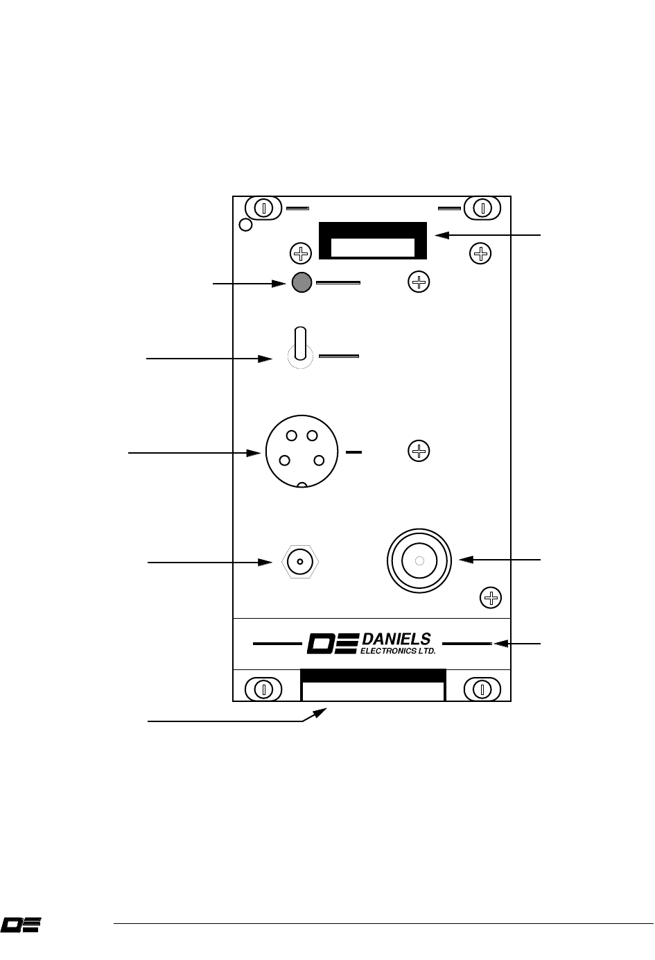
3.1 MT-3 Transmitter Front Panel
ELECTRONICS LTD.
DANIELS TM
3-1VHF Transmitter Instruction Manual
VT3150M1
ON / OFF SWITCH
TYPE N RF
OUTPUT JACK
SMA REFERENCE
INPUT JACK
TRANSMIT INDICATOR LED
TRANSMITTER
MODEL IDENTIFIER
FACTORY SET
OPERATING
FREQUENCY
MICROPHONE
CONNECTOR
TRANSMITTER
TX
REFERENCE
INPUT
OFF
NORM
KEY TX
MIC
RF OUT
FREQUENCY (MHz)
33.25000
MADE IN CANADA
VT-3/160-SWA8
MADE IN CANADA
MADE IN CANADA
RED TEXT
FREQUENCY (MHz)
160.00000
3 FINGER GASKET (2)
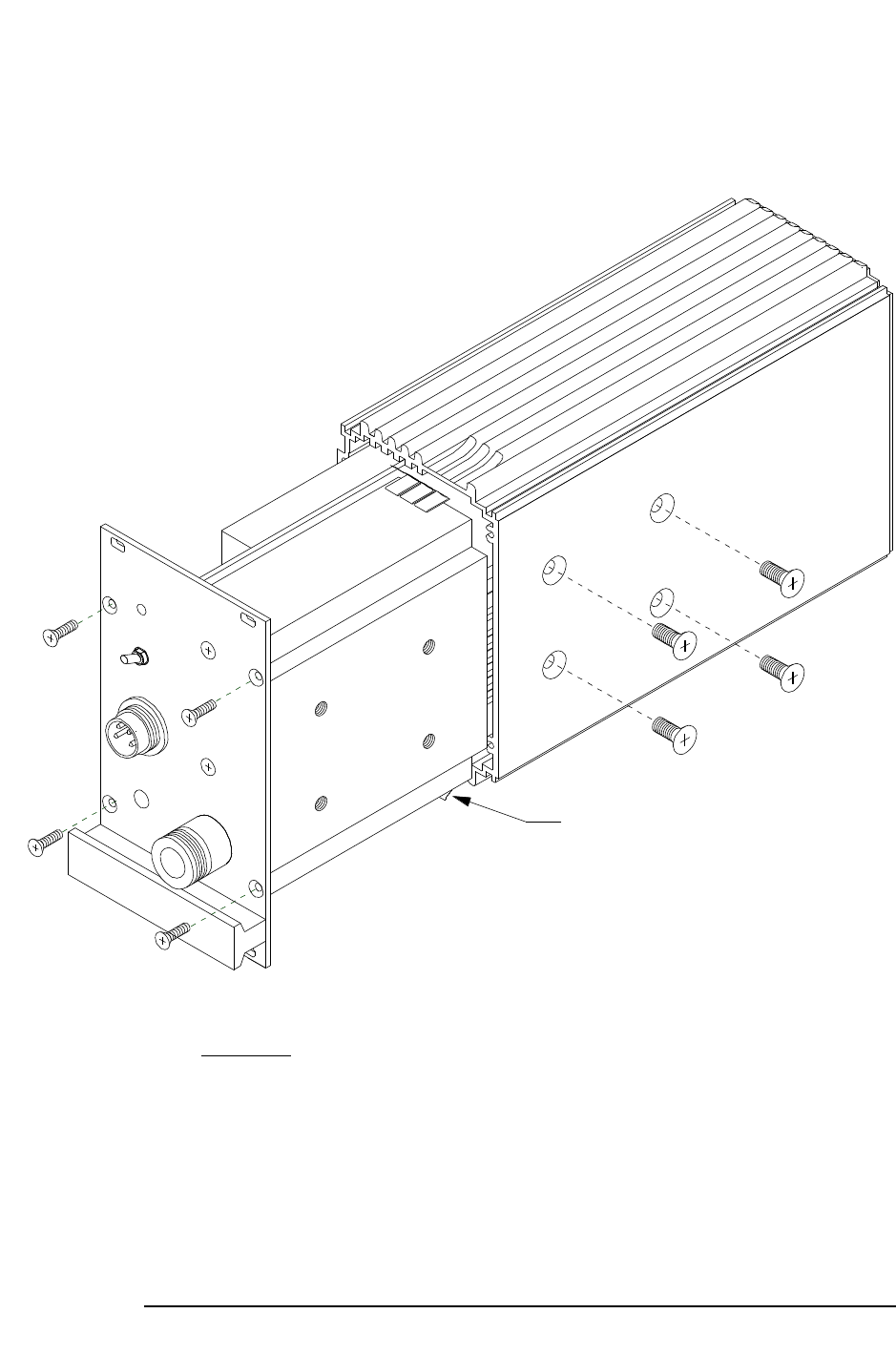
Instructions
1. Remove the four screws (A) in the Front panel.
2. Remove the four screws (B) on the side of the Transmitter Case.
A
A
A
A
B
B
B
B
MT3TXM2B
MT-3 Transmitter Case - Exploded View3.2
ELECTRONICS
3-2
DANIELS
DE VHF Transmitter Instruction Manual

VHF Enhanced Transmitter Instruction Manual VT-3 132 - 174 MHz
4-1
4
PARTS LIST
Description Part No. Qty.
LABEL/LEXAN,
14HP,
VHF: RED 3536-10111405 1

4-2
VHF Enhanced Transmitter Ins
truction Manual VT-3 132 - 174 MHz
This Page Intentionally Left Blank

VHF Enhanced Transmitter Instruction Manual VT-3 132 - 174 MHz
5-1
5
REVISION HISTORY
ISSUE DATE DESCRIPTION AND (REASON)
3 May 98 •
Manual formatted to modular style. All previous revision history in
issue 2.

5-2
VHF Enhanced Transmitter Instruction Manual VT-3 132 - 174 MHz
This Page Intentionally Left Blank

MT-3
RADIO
SYSTEMS
TRANSMITTER
MAIN BOARD
INSTRUCTION MANUAL
Covers:
Version 1.7 of the Transmitter Main Board
Version 1.6 & 1.8 of the FM Audio Processor Board
Copyright © 1998 Daniels
Electronics
Ltd.
All
rights
reserved.
No part of this
publication
may be
reproduced,
stored in a
retrieval
system or
transmitted
in any form or by any
means,
electronic,
mechanical,
photocopying,
recording or
otherwise,
without
the prior
written
consent of Daniels
Electronics
Ltd.
DE™ is a
registered
trademark
of Daniels
Electronics
Ltd.
registered
in the United States
Patent
and
Trademark
Office.
Issue: 3 Previous Issue: 2
Issue Date:
November
1998 Previous Issue Date: May 1998 Daniels
Electronics
Ltd.
Printing Date: January 2001
Victoria,
B.C.
Part No.: IM20-MT3TXMN PRINTED IN
CANADA

ii
Transmitter Main Board Instruction Manual
NOTE:
The user's
authority
to
operate
this
equipment
could be
revoked
through any
changes or
modifications
not expressly
approved
by Daniels
Electronics
Ltd.
The design of this
equipment
is subject to change due to continuous
development.
This
equipment
may
incorporate
minor changes in
detail
from the
information
contained
in this
manual.

Transmitter Main Board Instruction Manual
iii
TABLE OF CONTENTS
Page
1 GENERAL...................................................................................................................1-1
1.1
Introduction
....................................................................................................1-1
1.2
Performance
Specifications
.............................................................................1-1
1.2.1 General...............................................................................................1-1
1.2.2 Audio
Specifications
...........................................................................1-2
2 THEORY OF OPERATION........................................................................................2-1
2.1
Transmitter
Main Board..................................................................................2-1
2.1.1 General...............................................................................................2-1
2.1.2
Transmitter
Push-To-Talk...................................................................2-1
2.1.2.1 Microphone PTT....................................................................2-1
2.1.2.2 PTT With
Time-Out-Timer
.....................................................2-2
2.1.2.3 PTT No
Time-Out-Timer
........................................................2-2
2.1.2.4 Optional Relay........................................................................2-2
2.1.2.5 PTT Output.............................................................................2-3
2.1.2.6 PTT
Voltage
Switching
...........................................................2-3
2.1.2.7
Transmitter
Standby Modes....................................................2-3
2.1.3 Audio
Circuits
.....................................................................................2-4
2.1.3.1 Microphone
Audio
..................................................................2-5
2.1.3.2
Received
Audio
.......................................................................2-5
2.1.4 Channel
Selection
...............................................................................2-5
2.1.4.1 Synthesized
Transmitter
..........................................................2-5
2.1.4.2 Crystal
Controlled
Transmitter
................................................2-6
2.1.5
Amplifier
Circuits
...............................................................................2-6
2.1.6
Time-Out-Timer
Circuitry
...................................................................2-6
2.2 MT-3 Front Panel Board................................................................................2-8
2.3 MT-3 Audio Processor (Version 1.6).............................................................2-8
2.3.1 General...............................................................................................2-8
2.3.2 Power
Requirements
...........................................................................2-8
2.3.3 Audio Processor Turn-on
Time
..........................................................2-9
2.3.4 Audio Processor Signals.....................................................................2-9
2.3.4.1 Audio Processor Outputs........................................................2-9
2.3.4.2 Audio Processor
Modulation
Output......................................2-10
2.3.4.3 Audio Processor Low Frequency / Direct Mod. Output.........2-10
2.3.4.4 Audio Processor Inputs ..........................................................2-10
2.3.4.5 Audio Processor Microphone Input........................................2-11
2.3.4.6 Audio Processor
Balanced
Input.............................................2-11
2.3.4.7 Audio Processor
Auxiliary
Input............................................2-11
2.3.4.8 Audio Processor Subtone Inputs ............................................2-11
2.3.4.9 Audio Processor Direct
Modulation
Input..............................2-12
2.4 MT-3 Audio Processor (Version 1.8).............................................................2-12

iv
Transmitter Main Board Instruction Manual
2.4.1 General...............................................................................................2-12
2.4.2 Power
Requirements
...........................................................................2-12
2.4.3 Audio Processor Turn-on
Time
..........................................................2-13
2.4.4 Audio Processor Signals.....................................................................2-13
2.4.4.1 Audio Processor Outputs........................................................2-13
2.4.4.2 Audio Processor
Modulation
Output......................................2-14
2.4.4.3 Audio Processor Low Frequency / Direct Mod. Output.........2-14
2.4.4.4 Audio Processor Inputs ..........................................................2-14
2.4.4.5 Audio Processor Microphone Input........................................2-15
2.4.4.6 Audio Processor
Balanced
Input.............................................2-15
2.4.4.7 Audio Processor
Auxiliary
Input............................................2-15
2.4.4.8 Audio Processor Subtone Inputs ............................................2-15
2.4.4.9 Audio Processor Direct
Modulation
Input..............................2-16
2.5 Low Frequency
Modulation
............................................................................2-16
3
TRANSMITTER ALIGNMENT
.................................................................................3-1
3.1 General...........................................................................................................3-1
3.2 Repair Note.....................................................................................................3-1
3.3 Printed
Circuitboard
Numbering
Convention
..................................................3-1
3.4
Recommended
Test
Equipment
List................................................................3-1
3.5 Standard Factory Settings and Jumper
Configuration
.....................................3-2
3.5.1 MT-3
Transmitter
Board Factory
Configuration
.................................3-2
3.5.2 MT-3 Audio Processor Factory
Configuration
...................................3-3
3.6 MT-3
Transmitter
Board
Alignment
...............................................................3-4
3.6.1 General...............................................................................................3-4
3.6.2 MT-3
Transmitter
Board Test Points..................................................3-5
3.7 Module
Installation
and
Removal
....................................................................3-5
3.8 MT-3 Audio Processor
Alignment
..................................................................3-6
3.8.1 General...............................................................................................3-6
3.8.2 MT-3 Audio Processor Standard
Deviation
Adjustment
.....................3-6
3.9 Standard Factory Settings and Jumper
Configuration
.....................................3-8
3.9.1 MT-3 Audio Processor Factory Configuration (Version 1.8).............3-8
3.10 MT-3 Audio Processor
Alignment
(Version 1.8)............................................3-10
3.10.1 General...............................................................................................3-10
3.10.2 MT-3 Audio Processor Standard
Deviation
Adjustment
.....................3-10
3.11 Low Frequency
Modulation
Configuration
.....................................................3-11
3.11.1 MT-3
Transmitters
..............................................................................3-11
3.11.2 MT-3 Tr
ansmitter
Audio Processors ..................................................3-12
3.11.3 Synthesizer and Crystal
Controlled
Oscillator
....................................3-13
3.11.4 Tuning the
Transmitter
........................................................................3-14
4
TRANSMITTER INTERCONNECT PIN DEFINITIONS
........................................4-1
5 ILLUSTRATIONS AND SCHEMATIC DIAGRAMS..............................................5-1
5.1
Transmitter
Block Diagram.............................................................................5-1
5.2 Tra
nsmitter
Main Board
Electrical
Assembly..................................................5-3

Transmitter Main Board Instruction Manual
v
5.2.1
Transmitter
Main Board Top Side
Component
Layout.......................5-3
5.2.2
Transmitter
Main Board
Bottom
Side
Component
Layout..................5-4
5.2.3
Transmitter
Main Board
Schematic
Diagram......................................5-5
5.3 Front Panel Board...........................................................................................5-6
5.3.1 Front Panel Board
Component
Layout...............................................5-6
5.3.2 Front Panel Board
Schematic
..............................................................5-7
5.4 Audio Processor
Electrical
Assembly (Version 1.6) .......................................5-8
5.4.1 Audio Processor
Component
Layout..................................................5-8
5.4.2 Audio Processor
Schematic
Diagram..................................................5-9
5.5 Audio Processor
Electrical
Assembly (Version 1.8) .......................................5-10
5.5.1 Audio Processor
Component
Layout..................................................5-10
5.5.2 Audio Processor
Schematic
Diagram..................................................5-11
5.5.3 TX
Time-Out-Timer
Electrical
Assembly............................................5-12
5.5.3.1 TX
Time-Out-Timer
Component
Layout................................5-12
5.5.3.2 TX
Time-Out-Timer
Schematic
Diagram................................5-12
6 PARTS LISTS .............................................................................................................6-1
6.1
Transmitter
Main Board Parts List..................................................................6-1
6.1.1
Transmitter
Main Board
Electrical
Parts List......................................6-1
6.1.2
Transmitter
Main Board
Mechanical
Parts List...................................6-3
6.1.3 MT-3 Front Panel Board
Electrical
Parts List.....................................6-4
6.2 MT-3 Audio Processor Parts List (Version 1.7).............................................6-4
6.2.1 MT-3 Audio Processor
Electrical
Parts List (Version 1.6)..................6-4
6.3 MT-3 Audio Processor Parts List (Version 1.8).............................................6-6
6.3.1 MT-3 Audio Processor
Electrical
Parts List (Version 1.8)..................6-6
7 REVISION HISTORY.................................................................................................7-1

vi T
ransmitter Main Board Instruction Manual
This Page Intentionally Left Blank.

Transmitter Main Board Instruction Manual
1-1
1
GENERAL
invisible
text
1.1 Introduction
The MT-3
Transmitter
Main Board
integrates
the MT-3 Front Panel
Board,
MT-3
Audio
Processor, Synthesizer or Crystal
Controlled
Oscillator
module,
and
Amplifier
module
together
to
comprise a MT-3 series
transmitter
(see section 5.1: MT-3
Transmitter
Block Diagram). The Front
Panel Board and the Audio Processor are soldered
directly
to the
Transmitter
Main Board
while
the
Amplifier
and the Synthesizer or Crystal
Controlled
Oscillator
module are frequency band
sensitive,
plug-in modules.
Circuitry
and jumpers on the
Transmitter
Main Board control the
operation
of the
modules as
well
as the
overall
operation
of the MT-3
transmitter.
Power and signal
connections
are
made through the 48 pin type 'F'
connector
on the rear of the
Transmitter
Main Board
where
they
are then routed to the other MT-3 modules. The front and rear panels are
attached
to the
Transmitter
Main Board and
together
with
the extruded
aluminum
shell,
form the
transmitter
enclosure.
1.2
Performance Specifications
invisible
text
1.2.1
General
Type:
MT-3 Series Transmitter
Compatibility:
MT-3 Series Amplifier, OC-3 Crystal Controlled Oscillator
module, OS-3 and OS-3H Frequency Synthesizer modules.
Modulation:
11K0F3E or 16K0F3E (Frequency Modulation).
Operating Temperature Range:
-30˚C to +60˚C, optional -40˚C to +60˚C temperature test.
Operating Humidity:
95% RH (non-condensing) at +25°C.
Operating Voltage:
+9.5 Vdc Regulated. +13.8 Vdc Nominal (11 - 16 Vdc).
Front Panel Controls:
NORM (r
epeat mode), OFF, and KEY TX (Tx on).
PTT Activation:
• Active to ground with or without time-out-timer;
• Microphone activated with or without time-out-timer;
• Front Panel switch:
KEY TX - without time-out-timer;
• NORM - with or without time-out-timer.
• Isolated (optional relay) with or without time-out-timer.
PTT Time-Out-Timer:
Selectable from 1 sec. to 8 hrs. (Factory Default: 5 min.).

1-2
Transmitter Main Board Instructio
n Manual
1.2.2
Audio Specifications
Audio Input:
Balanced 600 ohm or unbalanced (optional).
Input level sensitivity, -25 dBm to 0 dBm.
Audio Response:
Pre-emphasis (6 dB per octave); +0.5 to -2.0 dB
from 300 Hz to 3 kHz;
Flat Audio Response:
+1 to -1 dB from 100 Hz to 3 kHz.
Audio Deviation:
Preset to ±1.5 kHz (Narrow Band) or ±3.0 kHz (Wide Band)
with a 1 kHz tone (capable ±2.5 kHz or ±5.0 kHz).
Subtone Audio Input 1:
0.5 Vpp at 200 Hz for ±500 Hz deviation
(internally adjustable).
Subtone Audio Input 1 Frequency range:
60 Hz to 300 Hz.
Subtone Audio Input 2:
0.5 Vpp at 100 Hz for ±500 Hz deviation
(internally adjustable).
Subtone Audio Input 2 Frequency range:
DC to 150 Hz.
Direct Modulation Input:
0.5 Vrms at 1 kHz or ±3 kHz deviation.
Direct Modulation Frequency range:
DC to 5 kHz.

Transmitter Main Board Instruction Manual
2-1
2
THEORY OF OPERATION
invisible
text
2.1
Transmitter Main Board
invisible
text
2.1.1
General
Switch
SW1 on the Front Panel Board is a DPDT
switch
which
controls the
operation
of the
transmitter
(refer to the operations section of the
Transmitter
Manual). When SW1 is in the 'OFF'
position the
transmitter
is turned off;
however,
+13.8
Vdc is
still
present on the
Transmitter
Main
Board as the
+13.8
Vdc supply is not
switched.
When SW1 is in the
'KEYED'
position,
+9.5
Vdc
is supplied to the
transmitter
circuitry
and the
transmitter
is
continuously
keyed on. When SW1 is
in the 'NORM'
position,
+9.5
Vdc is supplied to the
transmitter
circuitry
and the
transmitter
can be
keyed from any of the
several
Push-To-Talk inputs.
Refer to section 5.2.3
Transmitter
Main Board
Schematic
Diagram.
2.1.2
Transmitter Push-To-Talk
All
three of the Push-To-Talk (PTT) inputs that key the
transmitter
are
active
low (<
+2
Vdc). One
PTT input is on the front panel
microphone
connector.
The other two PTT inputs: PTT WTO
(PTT With
Time-Out-Timer)
and PTT NTO (PTT No
Time-Out-Timer),
are on the
backplane
connector
of the
transmitter
board. If
required,
the
microphone's
PTT input can be configured to
activate
the
transmitter's
Time-Out-Timer
(TOT). An
isolated
PTT input can be made
available
by
installing
an
optional
relay
(RELAY1)
and configuring jumpers J1 to J4 so that the relay controls
the PTT
circuitry.
2.1.2.1 Microphone PTT
Jumper J1 on the MT-3 Front Panel Board configures the
microphone's
PTT input (MIC PTT) to
either
bypass or
activate
the
transmitter's
TOT.
Installing
surface mount jumper J1 in the 'x'
position
(default)
selects the MIC PTT NTO line
which
bypasses the TOT.
Installing
surface
mount jumper J1 to the 'y' position selects the MIC PTT WTO line
which
activates
the
transmitter's
TOT. When SW1 is in the
'KEYED'
position the MIC PTT NTO line is a
utomatically
grounded.
Refer to Section 5.3.1, "MT-3 Front Panel Board
Component
Layout" for the
location
of jumper
J1.

2-2
Transmitter Main Board Instruction Manual
2.1.2.2
PTT With Time-Out-Timer
Pins B10 and Z10 of the
backplane
connector
are the PTT WTO input. When the PTT WTO
signal,
which
is
normally
high,
falls
below
+2.0
Vdc,
the
transmitter
is keyed. The
transmitter
is
disabled when the PTT WTO input rises
above
+2.3
Vdc or if the TOT's
time-out
period is
exceeded.
If the
time-out
period is
exceeded
the PTT WTO input must go high (>+2.3 Vdc) and
then low again in order to rekey the
transmitter.
The PTT WTO threshold of
approximately
+2
Vdc (0.3 Vdc hysteresis) is set by U1a,
R1, R2,
R3,
R4, R9,
and R10
while
diodes D1 and D2
provide
overvoltage
protection
for U1a. The PTT WTO
signal output from U1a is 'AND'ed
with
the MIC PTT WTO by U2a. When
either
the PTT WTO
or the MIC PTT WTO is
activated
the output of U2a goes low
which
triggers the
transmitter's
TOT
located
on the MT-3 Audio Processor. The TOT's output is 'AND'ed
with
the MIC PTT NTO
signal (U2c) and the PTT NTO signal (U2d). When any one of the
preceding
three signals (TOT's
output,
MIC PTT NTO, PTT NTO) go low the
transmitter
is
activated
by transistors Q1 to Q7
which
switch
power to the
various
modules.
2.1.2.3 PTT No Tim
e-Out-Timer
Pins B14 and Z14 of the
backplane
connector
are the PTT NTO input. When the PTT NTO
signal,
which
is
normally
high,
falls
below
+2.0
Vdc,
the
transmitter
is keyed. As long as the PTT NTO
signal remains
below
+2.0
Vdc the
transmitter
will
remain keyed. The
transmitter
is disabled when
the PTT NTO signal rises
above
+2.3
Vdc.
The PTT NTO threshold of
approximately
+2
Vdc (0.3 Vdc hysteresis) is set by U1b,
R5, R6,
R7,
R8, R9,
and R10
while
diodes D3 and D4
provide
overvoltage
protection
for U1b. The PTT NTO
signal is 'AND'ed
with
the output of U2c (MIC PTT NTO signal 'AND'ed
with
the TOT output) by
U2d. When the output of U2d goes low the
transmitter
is
activated
by transistors Q1 to Q7
which
switch
power to the
various
modules.
2.1.2.4 Op
tional Relay
The
transmitter's
PTT
circuitry
can be
completely
isolated
by
installing
RELAY1.
Jumpers J1 to J5
configure the relay to
provide
an
isolated
PTT input for
either
the PTT WTO line or PTT NTO line.
The
isolated
PTT input is
enabled
by
energiz
ing the relay. The
transmitter
board
will
accept
any of
the
Aromat
TF2E line relays. These relays are DPDT, single side
stable,
and
have
coil
voltages
ranging from
+3
Vdc to
+48
Vdc. Only one set of relay
contacts
are used to
activate
the PTT
circuitry.
To configure the
isolated
input for PTT WTO
operation
jumpers J2, J3, and J4 must be in the 'y'
position. In this
mode,
pins B10 and Z10 no longer function as the PTT WTO
input;
however,
pins
B14 and Z14
continue
to function as the normal PTT NTO input.

Transmitter Main Board Instruction Manual
2-3
To configure the
isolated
input for PTT NTO
operation
jumpers J2, J3, and J4, must be in the 'x'
position. In this
mode,
pins B14 and Z14 no longer function as the PTT NTO
input;
however,
pins
B10 and Z10
continue
to function as the normal PTT WTO input.
2.1.2.5 PTT Output
Pin B24 on the
backplane
connector
is an open drain output (Q9)
which
is pulled low
anytime
the
transmitter
is keyed and the synthesizer is locked. A crystal
controlled
transmitter
does not
have
a
locked
condition
so pin B24 is pulled low
anytime
the
transmitter
is keyed. Q9, an N-channel
MOSFET
capable
of sinking currents up to 2
Amps,
is
activated
by Q8
which
is
activated
by the
Qualified
PTT signal (JS2-6) of the Synthesizer or Crystal
Controlled
Oscillator
module. The
Qualified
PTT signal also controls the LED ENA line for diode D1 on the front panel board and
enable
line for the MT-3
Amplifier
Module (JP1-1).
2.1.2.6
PTT Voltage Switching
The PTT
voltage
switching
circuitry
is comprised of transistors Q1 through Q7 and the associated
resistors. The base of Q1 is
driven
by the output of U2d
which
is the
combined
PTT signal from
all of the PTT inputs. When the
transmitter
is
keyed,
Q1 is turned off and subsequently transistors
Q3, Q4, and Q6 are turned on. Transistors Q3, Q4, and Q6
provide
three
different
functions:
• Q3
provides
the
active
low signal for the Synthesizer or Crystal
Controlled
Oscillator
module PTT
input;
• Q4 turns on Q5
which
turns on the
+9.5
Vdc
Switched
supply;
• Q6 turns on Q7
which
turns on the
+9.
5 Vdc PTT
Switched
supply.
The
'+9.5
Vdc
Switched'
supply (Q5) can also be
activated
by
installing
jumper J6 or by
externally
grounding the TX Standby Line (pins B12 and Z12). The
'+9.5
Vdc PTT
Switched'
supply and the
'+9.5
Vdc
Switched'
supply both pro
vide
+9.5
Vdc but depending on how jumpers J6, J7 and J18
are configured the
transmitter's
standby mode
will
change.
2.1.2.7
Transmitter Standby Modes
The MT-3 series
transmitters
have
four
different
standby modes that trade-off standby current
consumption
for start-up speed. The standby modes are
determined
by three jumpers: jumper J6
which
always
turns on the
'+9.5
Vdc
Switched'
supply,
jumper J7
which
selects the power source
for the MT-3 Audio Processor and jumper J18
which
selects the
enable
line for the OS-3 or OS-
3H
Synthesizer,
or OC-3 Crystal
Controlled
Oscillator
module.
The actual current and start-up time may depend on the
oscillator
source (crystal or synthesizer)
and
amplifier
module. The current and start-up times given below are represe
ntative
values

2-4
Transmitter Main Board Instruction Manual
intended
only as a
guideline.
Refer to the
instruction
manual for the transmitter that came with
your system for
specifications.
• MODE 1:Jumper J6 out
- the audio processor is
switched
by a PTT signal
- the synthesizer or crystal
controlled
oscillator
is
switched
by a PTT signal
- standby
current:
Synthesized -
typically
7 mA
Crystal
Controlled
-
typically
6 mA
- start-up
time:
Synthesized -
typically
50 ms
Crystal
Controlled
-
typically
25 ms
• MODE 2:Jumper J6
in,
jumper J7 in the 'y'
position,
jumper J18 in the 'x' position
- the audio processor is
switched
by a PTT signal
- the synthesizer or crystal
controlled
oscillator
is
enabled
all of the
time
- standby
current:
Synthesized -
typically
65 mA
Crystal
Controlled
-
typically
25 mA
- start-up
time:
Synthesized -
typically
25 ms
Crystal
Controlled
-
typically
25 ms
• MODE 3:Jumper J6
in,
jumper J7 in the 'x'
position,
jumper J18 in the 'y' position
- the audio processor is enabled all of the
time
- the synthesizer or crystal
controlled
oscillator
is
switched
by a PTT signal
- standby
current:
Synthesized - not used in this mode
Crystal
Controlled
-
typically
28 mA
- start-up
time:
Synthesized - not used in this mode
Crystal
Controlled
-
typically
10 ms
• MODE 4:Jumper J6
in,
jumper J7 in the 'x'
position,
jumper J18 in the 'x' position
- the audio processor is
enabled
all of the
time
- the synthesizer or crystal
controlled
oscillator
is
enabled
all of the
time
- standby
current:
Synthesized -
typically
90 mA
Crystal
Controlled
-
typically
46 mA
- start-up
time:
Synthesized -
typically
10 ms
Crystal
Controlled
-
typically
10 ms
2.1.3
Audio Circuits
All
of the audio signal co
nditioning
(e.g.
limiting,
filtering,
and pre-emphasis) is performed by the
MT-3 Audio Processor. The
transmitter
board routes the audio lines from the
backplane
connector
to the audio processor and then to the synthesizer. The audio lines routed to the audio processor
are: two subtone inputs
(backplane
pins B22 and
Z24),
a
direct
modulation
input (pin
Z28),
a
squelched/flat
audio input (pin
Z20),
a 600 ohm
balanced
input (pins B18 and
Z18),
and an audio
control line (pin Z22). The audio processor's balanced input pins are
isolated
from pins B18 and

Transmitter Main Board Instruction Manual
2-5
Z18 by a transformer (T1). Two audio outputs from the MT-3 Audio Processor are routed to the
synthesizer or crystal control
oscillator
modules.
2.1.3.1 Microphone Audio
Normally the audio from a
transmitt
er's
microphone
is
transmitted
by that
transmitter;
however,
the
Transmitter
Main Board can be configured by the MIC IN and MIC OUT lines so that the audio
from an
external
microphone
modulates
transmitter.
The
configuration
of the MIC IN (pin Z4) and
MIC OUT (pin B4) lines on the MT-3
Transmitter
Board are
controlled
by jumpers J16 and J17
respectively.
Jumper J16 selects the audio source for the MT-3 Audio Processor's
microphone
input. Jumper J17 is used to
enable
or disable the MIC OUT line. Normally the
transmitter's
microphone
is
selected
(J16 in the 'x' position) and the MIC OUT line is
enabled
(J17 is
installed).
2.1.3.2 Received Audio
Pin B20 is the audio input from the
transmitter's
corresponding
receiver.
The
default
setting
for
this line is to
have
it AC coupled (Jumper J9 is out) and
directly
connected
to the front panel board
RX AUDIO line (jumpers J10 and J11 in the 'x' position). Audio
amplifier
U5 can be
enabled
by
installing
jumper J8
which
connects power to U5 (continuously in the 'x'
position,
PTT
switched
in
the 'y' position).
Setting
jumper J10 in the 'y' position and jumper J11 in the 'z' position enables the
audio path through the
amplifier.
Level
control for the
squelched,
de-emphasized
audio input line is
provided
by R27. Audio
amplifier
U5 draws
approximately
5 mA so it is not
normally
enabled.
2.1.4
Channel Selection
invisible
text
2.1.4.1
Synthesized Transmitter
Seven
backplane
connections
are used to
communicate
with
the synthesizer unit. Pins D28, D30,
and D32 are used (in house) to program the synthesizer. Channel
select
lines CSEL 0 (least
significant
bit) through CSEL 3 (most
significant
bit),
which
are
available
at pins D20, D22, D24,
and D26, are used once the synthesizer is
programmed
to
select
one of 16 channels. If the
channel
select
lines are all low
(channel
0) the
channel
for the synthesizer is read from
switches
FSW1
(most
significant),
FSW2, FSW3, and
FSW4
(least
significant);
otherwise
one of 15 pre-
programmed
frequencies
is
selected.
Since the resulting frequency is
dependent
on the
transmitter
model,
refer to the section on frequency
selection
in the
Transmitter
Manual or to the
channel
designation
tables for that
particular
transmitter.

2-6
Transmitter Main Board Instruction Manual
2.1.4.2
Crystal Controlled Transmitter
The OC-3 Crystal Control
Oscillator
module is a
direct
replacement
for the synthesizer module and
therefore
uses the same
connections
as the synthesizer to connects to the MT-3
Transmitter
Main
Board. The
channel
select
lines and
switches
FSW1
to
FSW4
are not used by the crystal control
module as the
transmitter's
operating
frequency is
determined
by the Crystal Control
Oscillator
module's crystal frequency. A frequency
multiplication
factor,
described in the
manual
for this
module,
relates
the crystal frequency to the operating frequency .
2.1.5
Amplifier Circuits
The MT-3 series
Amplifier
has 6
connections
that are
cabled
to the
transmitter
board:
+13.8
Vdc,
+9.5
Vdc,
Enable,
Forward Power Sense,
Reverse
Power Sense, and Ground. The
+13.8
Vdc
supply (JP1-3) is
always
on
while
the
+9.5
Vdc supply (JP1-2) is
always switched
by a PTT
signal. The
enable
line (JP1-1) is
active
low and is
controlled
by the
Qualified
PTT signal from
the synthesizer module or crystal
controlled
oscillator
module.
Jumpers J12, J13, J14, and J15 are used to configure the
amplifier's
forward and
reverse
power
sense lines (JP1-4 and JP1-5). Normally jumpers J13, J14, and J15 are in the 'x' position
which
directly
connects the
amplifier's
forward and
reverse
power sense lines to the
backplane
connector
(pins B26 and Z26
respectively).
The forward and
reverse
power sense lines from the
Amplifier
can be open
collector
or
linear
outputs depending on how they are configured in the
amplifier
module. In open
collector
configuration
the lines are
active
low,
that
is,
the output
will
go low
when a
'fail'
condition
is
detected.
If both lines from the
amplifier
module are configured as open
collector
outputs,
the power sense lines can be 'OR'ed
together
to make a
general
fail
indicator
(jumper J12
in,
jumpers J13, J14, and J15 in the 'y' position). The Fail
Indicator
is also an open
collector
output;
however,
the Fail
Indicator
is
active
high (the output goes high when a
'fail'
condition
is
detected).
When the
transmitter
is configured
with
the
general
fail
indicator
option,
pin Z26 (VSWR
reverse)
is not used and pin B26 becomes the Fail
Indicator
output.
2.1.6
Time-Out-Timer Circuitry
The MT-3
Transmitter
also has an
associated
programmable
push-to-talk (PTT)
time-out-timer
(TOT)
circuitry
on the Tra
nsmitter
Main Board. The TOT
circuitry
is
powered
via
J34 from the
continuous
+9.5
Vdc supply and is
programmable
for
various
time
-out periods.
The TOT input trigger
(enabled
by J33) is
normally
high and in this state the
timer
is disabled.
When the input trigger
level
falls
below
+2.0
Vdc,
the
timer
is
activated,
the TOT output trigger
(enable
by J35) is pulled
low,
and the
transmitter
is keyed. If the input trigger rises
above
+2.4
Vdc
or if the
time-out
period is
exceeded,
the output trigger
will
go
high,
disabling
the
transmitter.
If the
time-out
period is
exceeded,
the TOT input trigger must go high and then low again in order to
rekey the
transmitter.
Transmitter Main Board Instruction Manual
2-7
The
time-out
duration is jumper
selectable
from 1 second to 8 hours. The positions of the jumpers
on the top (Through hole
component)
side of the
Transmitter
Main Board.
Table
2-1 shows the
time-out
duration in
minutes
for the
various
jumper settings
which
are
listed
as
enabled
(E: jumper
shorted - in) or disabled (D: jumper left open - out). The standard factory
setting
of 5
minutes
is
shown in bold type in
table
2-2.
Table
2-1
Time-Out-Timer
Settings
D = DISABLED (no solder jumper
installed),
E = ENABLED (solder jumper
installed).
Bold text
represents
default
settings.
TIME-OUT DURATION
(MINUTES)
J26 = E
J26 =
D
J26 =
E
J32
J31
J29
J28
J27 = D
J27 =
E
J27 =
E
E E E E 0.01 0.01 0.01
E E E D 0.02 0.03 0.01
E E D E 0.04 0.06 0.02
E E D D 0.08 0.12 0.05
E D E E 0.15 0.23 0.10
E D E D 0.31 0.47 0.19
E D D E 0.62 0.94 0.38
E D D D 1.25 1.88 0.75
D E E E 2.5 3.75 1.5
D E E D
5.0
7.5 3.0
D E D E 10 15 6.0
D E D D 20 30 12
D D E E 40 60 24
D D E D 80 120 48
D D D E 160 240 96
D D D D 320 480 192

2-8
Transmitter Main Board Instruction Manual
2.2 MT-3 Front Panel Board
The MT-3 Front Panel Board is a subsection of the MT-3
Transmitter
Board
which
is used to
mount the front panel
switch,
diode,
and
microphone
connector.
The main purpose of the board is
to
eliminate
a
wiring
harness for the front panel components. Jumper J1,
located
on the rear of the
circuitboard,
is used to
select
whether
or not the MIC PTT line
activates
the
transmitter's
TOT.
Jumper J2 is used to
select
whether
or not Rx Audio or 13.8
Volt
is supplied to pin 4 of the
microphone.
• Jumper J1: 'x' position MIC PTT NTO no
time-out-timer
(factory setting)
'y' position MIC PTT WTO
with
time-out-timer
• Jumper J2: 'x' position Rx Audio
enabled
to MIC-4 pin (factory setting)
'y' position
+13.8
Volts
supplied to MIC-4 pin
Refer to section 5.3.2 "MT-3 Front Panel Board
Schematic
Diagram".
2.3 MT-3 Audio Processor (Version 1.6)
invisible
text
2.3.1
General
The MT-3 Audio Processor is a
versatile
circuitboard
that can
provide
several
types of audio
processing for
voice
or data transmission. Two analog
switches
on the audio processor, co
ntrolled
by a common
signal,
make it possible to
transmit
voice
or data. A continuous
+9.5
Vdc supply
and a
switched
+8.0
Vdc supply are required to power the module. The MT-3 Audio Processor is
backwards
compatible
to Daniels
Electronics
MT-2 series tr
ansmitters.
Refer to section 5.4.1
"MT-3 Audio Processor
Component
Layout" and to section 5.4.2 "MT-3 Audio Processor
Schematic
Diagram" for
component
location
and
designation
references.
2.3.2
Power Requirements
The audio processor can be configured for continuous audio standby or for
switched
audio standby
by the
Transmitter
Main Board. If fast audio
risetime
is
desired,
the
transmitter
should be
operated
in standby mode 2 or 3 as
specified
in section 2.1.2.7. Power for the
microphone
input and the
balanced
input can be
separately
disabled by jumpers J3 and J4
respectively
if the input is not
required. This results in a current savings of
approximately
11 mA per input. The current
requirements
for the MT-3 Audio Processor are shown in
Table
2-1. The current for the
associated
TOT is
approximately
4 mA when the
transmitter
is keyed and is
included
in the keyed
values
in the
table
below.

Transmitter Main Board Instruction Manual
2-9
Table
2-1 MT-3 Audio Processor Current Consumption.
Function Current Draw
keyed / unkeyed
Switched
Audio
Standby
Both Microphone and
Balanced
Input
enabled
29.0 / 0.5 mA
Only Microphone or
Balanced
Input
enabled
17.5 / 0.5 mA
Only
Auxiliary
Input
enabled
6.0 / 0.5 mA
Continuous
Audio
Standby
Both Microphone and
Balanced
Input
enabled
29.0 / 25.5 mA
Only Microphone or
Balanced
Input
enabled
17.5 / 14.0 mA
Only
Auxiliary
Input
enabled
6.0 / 2.5 mA
2.3.3
Audio Processor Turn-on Time
The turn-on
time
of the audio processor is 25 ms. This
measurement
is made
with
the standard
factory settings with a 1 kHz tone
applied
to the
balanced
input. The turn-on
time
is the
time
it
takes the audio processor to output a stable audio signal from the
time
its power
(+9.5
Vdc) is
switched
on. The turn-on
time
can be
virtually
eliminated
by configuring the audio processor for
continuous audio standby (see section 2.1.2.7
Transmitter
Standby Modes).
2.3.4
Audio Processor Signals
The MT-3 Audio Processor has six audio
inputs,
two audio outputs and one audio control input.
Five
of the audio inputs are used p
rimarily
for
voice
signals. The
sixth,
the Direct
modulation
input,
is used
primarily
for data signals. The audio control input is used to
switch
audio outputs so the
transmitter
can
transmit
voice
or data.
2.3.4.1 Audio Processor Outputs
Both the audio
outputs,
Modulation
Output (P3-1) and Low Frequency / Direct
Modulation
Output
(P4-2), are gated by audio
switches
U9 and U10
respectively
which
are
controlled
by the Tx
Audio
Control Input (P4-4). The audio
switches
operate
complimentary
to each other so there can
ever
only be one source
modulating
the
transmitter.
In standard
configuration,
the
Modulation
Output
port is used so
switch
U9 is
always
on.

2-10
Transmitter Main Board Instruction Manual
2.3.4.2
Audio Processor Modulation Output
The
Modulation
Output port is the output port used by all
voice
input signals. The
voice
inputs are
combined
by summing
amplifier
U4a
which
has an
associated
symmetry control (R14). Op-amp
U4a
together
with
U5a
provide
the
limiting
action
for the audio processor.
After
the audio signals
have
been
combined
and
limited,
they are
filtered
by a 6 pole lowpass
Butterworth
filter
(U5b, U5c,
and U5d). Jumpers JU24, JU25 and JU26 configure the lowpass
filter
for
narrowband
or
wideband
operation:
jumpers JU24(x and y) to JU26(x and y) are
installed
for
wideband
(25 kHz)
channels and are not
installed
for
narrowband
(12.5 kHz) channels. The output signal from the
filter
is then
level
adjusted by the
deviation
control
pot,
R29,
before
modulating
the
transmitter.
In
special
applications,
jumper JU6 can be disabled and JU7
enabled,
this
allows
the
transmitter
to
be
modulated
directly
from the
auxiliary
input. This should not be done
without
external
filtering
since jumper JU7 bypasses the
limiting
and
filter
circuits.
2.3.4.3 Audio Processor Low Frequency / Direct Mod. Output
The Low Frequency / Direct
Modulation
Output port has two functions depending on
whether
the
transmitter
is synthesized or crystal
controlled.
In a synthesized
transmitter,
this port is used to
modulate
the synthesizer
reference
frequency. The frequency response of this port is
typically
DC
to 60 Hz. In a crystal
controlled
transmitter,
this port can be used by the Direct
Modulation
Input
to
directly
modulate
the crystal control
oscillator
module. The frequency response of this port is
essentially
flat from DC to 5 kHz
with
no
limiting
or
filtering.
Amplification,
if
desired,
is
provided
by Op-amp U8a
which
is
powered
independent
of the audio card
voice
circuits
by jumper JU1.
2.3.4.4 Audio Processor Inputs
As
previously
mentioned,
the MT-3 Audio Processor has six audio
inputs,
five
used
primarily
for
voice
signals and one for data signals.
The 6 audio inputs on the audio processor are:
•
dynamic
microphone
input
• 600 ohm
balanced
input
• 2 subtone inputs
•
auxiliary
input.
•
direct
modulation
input.

Transmitter Main Board Instruction Manual
2-11
2.3.4.5 Audio Processor Microphone Input
The
microphone
input has an
automatically
gain
controlled
(AGC)
preamplifier
whose input
level
is
controlled
by R2. The
microphone
input
level
control (R2) can
accommodate
a -25 dBm to 0 dBm
input signal. The compression
level
for the
microphone
input is adjusted by R8. The
microphone
input is
limited
and
filtered
and is output at the standard
modulation
output port.
2.3.4.6 Audio Processor Balanced Input
The 600 ohm
balanced
input also has an AGC
preamplifier,
input
level
control (R31), and
compression
level
control (R38). The
balanced
input
level
control can
accommodate
a -25 dBm to
0 dBm input. The
balanced
input can
have
a standard 6
dB/octave
pre-emphasis response by
enabling
jumper JU9 or a
flat-audio
response by
enabling
jumper JU10. Like the
microphone
input,
the
balance
input is
limited
and
filtered
and is output at the standard
modulation
output port.
2.3.4.7 Audio Processor Auxiliary Input
The
auxiliary
input is a
special
input and does not
have
an AGC
preamplifier
or an input
level
control. This input can be configured for a pre-emphasis response
(enable
JU14) or a
flat-audio
response
(enable
JU15). The compression
level
for this input is set by R48. The auxiliary output
is
normally
summed
with
the
voice
signals by op-amp U4a,
limited,
then
filtered
and output at the
standard
modulation
output port. When jumper JU6 is disabled and jumper JU7 is
enabled,
the
auxiliary
input can be used to
directly
modulate
the
transmitter.
Care should be taken when
directly
modulating
the
transmitter
with
the
auxiliary
input because the MT-3
transmitters
use
direct
FM
modulation
and there is no
filtering
or
limiting
action
provided
by the
auxiliary
input. The input
level
to the
auxiliary
input should be -18 dBm and can be
driven
by one of three inputs:
• the
balanced
input – JU11
enabled
• the
tone/digital
input – JU12
enabled
• the
direct
modulation
input – JU13
enabled
When the 600 ohm
balanced
input is
connected
to the
auxiliary
input,
the
balanced
input
level
control can be used to adjust the
level
for the
auxiliary
input. When
either
the
tone/digital
input or
the
direct
modulation
input are used, the input
level
is not
adjustable.
2.3.4.8 Audio Processor Subtone Inputs
There are two subtone inputs
available
on the audio processor. Both subtone inputs can be
individually
configured to be output from the standard
Modulation
Output port or to be output from
the Low Frequency / Direct
Modulation
Output. In standard co
nfiguration,
Subtone 1 is summed

2-12
Transmitter Main Board Instruction Manual
with
the
voice
signals to be output from the standard
Modulation
Output port
while
Subtone 2 is
not used. Both subtone inputs
have
an input
level
control.
2.3.4.9
Audio Processor Direct Modulation Input
The Direct Modulation Input is an
extremely
versatile
input. This port is designed to be used for
data signals. Depending on the
application,
the signal can be
amplified,
AC or DC coupled and
output to the
Modulation
Output or the Low Frequency / Direct
Modulation
Output port. Please
consult the factory for
specific
jumper settings for your
application.
2.4 MT-3 Audio Processor (Version 1.8)
invisible
text
2.4.1
General
The MT-3 Audio Processor is a
versatile
circuitboard
that can
provide
several
types of audio
processing for
voice
or data transmission. Two analog
switches
on the audio processor,
controlled
by a common
signal,
make it possible to
transmit
voice
or data. A continuous
+9.5
Vdc supply
and a
switched
+8.0
Vdc supply are required to power the module. The MT-3 Audio Processor is
backwards
compatible
to Daniels
Electronics
MT-2 series
transmitters.
Refer to section 5.5.1
"MT-3 Audio Processor
Component
Layout" and to section 5.5.2 "MT-3 Audio Processor
Schematic
Diagram" for
component
location
and designation
references.
2.4.2
Power Requirements
The audio processor can be configured for continuous audio standby or for
switched
audio standby
by the
Transmitter
Main Board. If fast audio
risetime
is
desired,
the
transmitter
should be
operated
in standby mode 2 or 3 as
specified
in section 2.1.2.7
with
JU36 on the audio processor in the 'y'
position. Power for the
microphone
input and the
balanced
input can be disabled by jumpers JU36
and JU40
respectively
if the input is not required. This results in a current savings of
approximately
3.5 mA per input. The current
requirements
for the MT-3 Audio Processor are
shown in
Table
3-1. The current for the
associated
TOT is
approximately
4 mA when the
transmitter
is keyed. The keyed
values
in the
table
below do not
include
the current for the TOT.

Transmitter Main Board Instruction Manual
2-13
Table
3-1 MT-3 Audio Processor Current Consumption.
Function Current Draw
keyed / unkeyed
Switched
Audio
Standby
Both Microphone and
Balanced
Input
enabled
6.0 / 0.3 mA
Only Microphone or
Balanced
Input enabled 4.5 / 0.3 mA
Only
Auxiliary
Input
enabled
3.0 / 0.3 mA
Continuous
Audio
Standby
Both Microphone and
Balanced
Input
enabled
6.0 / 3.5 mA
Only Microphone or
Balanced
Input
enabled
4.5 / 1.5 mA
Only
Auxiliary
Input
enabled
3.0 / 0.5 mA
2.4.3
Audio Processor Turn-on Time
The turn-on
time
of the audio processor is 25 ms. This
measurement
is made
with
the standard
factory settings
with
a 1 kHz tone
applied
to the
balanced
input. The turn-on
time
is the
time
it
takes the audio processor to output a stable audio signal from the
time
its power
(+9.5
Vdc) is
switched
on. The turn-on
time
can be
virtually
eliminated
by configuring the audio processor for
continuous audio standby (see section 2.1.2.7
Transmitter
Standby Modes).
2.4.4 Audio
Processor Signals
The MT-3 Audio Processor has six audio
inputs,
two audio outputs and one audio control input.
Five
of the audio inputs are used
primarily
for
voice
signals. The
sixth,
the Direct
modulation
input,
is used
primarily
for data signals. The audio control input is used to
switch
audio outputs so the
transmitter
can
transmit
voice
or data.
2.4.4.1 Audio Processor Outputs
Both the audio
outputs,
Modulation
Output (P3-1) and Low Frequency / Direct
Modulation
Output
(P4-2), are gated by audio
switches
U9 and U10
respectively
which
are
controlled
by the Tx
Audio
Control Input (P4-4). The audio
switches
operate
complimentary
to each other so there can
ever
only be one source
modulating
the
transmitter.
In standard
configuration,
the
Modulati
on Output
port is used so
switch
U9 is
always
on.

2-14
Transmitter Main Board Instruction Manual
2.4.4.2
Audio Processor Modulation Output
The
Modulation
Output port is the output port used by all
voice
input signals. The
voice
inputs are
combined
by U1, a gain
level
programmable
compandor
which
is configured as an
automatic
level
control
amplifier.
Op-amp U4a
together
with
U5a
provide
the
limiting
action
for the audio
processor.
After
the audio signals
have
been
combined
and
limited,
they are
filtered
by a 6 pole
lowpass
Butterworth
filter
(U5b, U5c, and U5d). Jumpers JU24, JU25 and JU26 configure the
lowpass
filter
for
narrowband
or
wideband
operation:
jumpers JU24(x and y) to JU26(x and y) are
installed
for
wideband
(25 kHz) channels and are not
installed
for
narrowband
(12.5 kHz)
channels. The output signal from the
filter
is then
level
adjusted by the
deviation
control
pot,
R29,
before
modulating
the
transmitter.
In
special
applications,
jumper JU6 can be disabled and JU7
enabled,
this
allows
the
transmitter
to
be
modulated
directly
from the
auxiliary
input. This should not be done
without
external
filtering
since jumper JU7 bypasses the
limiting
and
filter
circuits.
2.4.4.3
Audio Processor Low Frequency / Direct Mod. Output
The Low Frequency / Direct
Modulation
Output port has two functions depending on
whether
the
transmitter
is synthesized or crystal
controlled.
In a synthesized
transmitter,
this port is used to
modulate
the synthesizer
reference
frequency. The frequency response of this port is
typically
DC
to 300 Hz. In a crystal
controlled
transmitter,
this port can be used by the Direct
Modulation
Input
to
directly
modulate
the crystal control
cscillator
module. The frequency response of this port is
essentially
flat from DC to 5 kHz
with
no
limiting
or
filtering.
Amplific
ation,
if
desired,
is
provided
by Op-amp U3b.
2.4.4.4 Audio Processor Inputs
As
previously
mentioned,
the MT-3 Audio Processor has six audio
inputs,
five
used
primarily
for
voice
signals and one for data signals.
The 6 audio inputs on the audio processor are:
•
dynamic
microphone
input
• 600 ohm
balanced
input
• 2 subtone inputs
•
auxiliary
input.
•
direct
modulation
input.

Transmitter Main Board Instruction Manual
2-15
2.4.4.5 Audio Processor Microphone Input
The
microphone
input has an
automatically
level
controlled
(ALC)
preamplifier
U1 whose input
level
is
controlled
by R2. The
microphone
input
level
control (R2) can
accommodate
a -25 dBm to
0 dBm input signal. The
microphone
input is
limited
and
filtered
and is output at the standard
modulation
output port. The
microphone
input can
have
a standard
6dB/octave
pre-emphasis
response or a
flat-audio
response, jumper JU3 at 'x' and 'y' position
respectively.
2.4.4.6 Audio Processor Balanced Input
The 600 ohm
balanced
input also uses the ALC
preamplifier
U1,
with
input
level
control pot (R31).
The
balanced
input
level
control can
accommodate
a -25 dBm to 0 dBm input. Like the
microphone
input,
the
balance
input is
limited
and
filtered
and is output at the standard
modulation
output port.
2.4.4.7 Audio Processor Auxiliary Input
The
auxiliary
input is a
special
input and does not
have
an ALC
preamplifier
or an input
level
control. This input can be configured for a pre-emphasis response
(enable
JU14) or a
flat-audio
response
(enable
JU15). The compression
level
for this input is set by R48. The
auxiliary
output
is
normally
summed
with
the
voice
signals by op-amp U4a,
limited,
then
filtered
and output at the
standard
modulation
output port. When jumper JU6 is disabled and jumper JU7 is
enabled,
the
auxiliary
input can be used to
directly
modulate
the
transmitter.
Care should be taken when
directly
modulating
the
transmitter
with
the
auxiliary
input because the MT-3
transmitters
use
direct
FM
modulation
and there is no
filtering
or
limiting
action
provided
by the
auxiliary
input. The input
level
to the
auxiliary
input should be -18 dBm and can be
driven
by one of three inputs:
• the
balanced
input – JU11 'x' position
• the
tone/digital
input – JU12
enabled
• the
direct
modulation
input – JU13
enabled
When the 600 ohm
balanced
input is
connected
to the
auxiliary
input,
the
balanced
input
level
control can be used to adjust the
level
for the
auxiliary
input. When
either
the
tone/digital
input or
the
direct
modulation
input are used, the input
level
is not
adjustable.
2.4.4.8
Audio Processor Subtone Inputs
There are two subtone inputs
available
on the audio processor. Both subtone inputs can be
individually
configured to be output from the standard
Modulation
Output port or to be output from
the Low Frequency / Direct Modulation Output. In standard
configuration,
Subtone 1 is summed
with
the
voice
signals to be output from the standard
Modulation
Output port
while
Subtone 2 is
not used. Both subtone inputs
have
an input
level
control.

2-16
Transmitter Main Board Instruction Manual
2.4.4.9 Audio Processor Direct Modulation Input
The Direct
Modulation
Input is an
extremely
versatile
input. This port is designed to be used for
data signals. Depending on the
application,
the signal can be
amplified,
AC or DC coupled and
output to the
Modulation
Output or the Low Frequency / Direct
Modulation
Output port. Please
consult the factory for
specific
jumper settings for your
application.
2.5 Low Frequency Modulation
The
transmitter
has an
additional
option to address low frequency user
modulation
requirements.
A
phase modu
lated
bandwidth
from 0 (dc) to 100 Hz (PLL loop
filter
bandwidth)
allows
specialized
applications
such as paging or trunking
where
a
separate
low frequency
digital/analog
modulation
channel
is required. Low Frequency
Modulation
allows
external
access to the low frequency
modulation
capabilities
of the synthesizer module. The DIRECT MODULATION inputs on the J1
control
connector
of the M-3
motherboard
will
be used (B20 for TX
A,
and A20 for
TX B). See section 3.11,
'Low
Frequency
Modulation
Configuration
' for set up and
alignment.

Transmitter Main Board Instruction Manual
3-1
3
TRANSMITTER ALIGNMENT
3.1
General
Transmitter
alignment
is
simplified
by using an M-3
Subrack,
SM-3 System
Monitor,
and RF
extender
cable
to
provide
transmitter
power and signal
interconnection.
Alternatively,
+9.5
Vdc and
+13.8
Vdc may be
applied
directly
to a
transmitter
module through
positive
connection
for the
+9.5
Vdc to pins B6 and
Z6,
for the
+13.8
Vdc to pins B2 and
Z2,
and
negative
connection
to pins
B30,
Z30,
B32,
and Z32.
Transmitter
balanced
audio (600 Ω) is
available
at pins B18 and Z18.
3.2 Repair Note
MT-3
Transmitter
modules are
mainly
made up of surface mount
devices
which
should not be
removed
or
replaced
using an ordinary soldering iron.
Removal
and
replacement
of surface mount
components should be performed only
with
specifically
designed surface mount rework and repair
stations
complete
with
ElectroStatic
Dissipative
(ESD)
protection.
When
removing
Surface Mount Solder Jumpers, it is
recommended
to use solder braid in
place
of
manual
vacuum
type desoldering tools when
removing
jumpers. This
will
help
prevent
damage
to
the
circuitboards.
3.3
Printed Circuitboard Numbering Convention
To ease
troubleshooting
and
maintenance
procedures,
Daniels
Electronics
Limited
has adopted a
printed
circuitboard
(PCB) numbering
convention
in
which
the last two digits of the
circuitboard
number represent the
circuitboard
version.
For
example:
• PCB number 43-912010
indica
tes
circuitboard
version
1.0;
• PCB number 50002-02
indicates
circuitboard
version
2.0.
All
PCB's
manufactured
by Daniels
Electronics
are
identified
by one of the
above
conventions.
3.4 Recommended Test Equipment List
Alignment
of the
complete
transmitter requires the
following
test
equipment
or its
equivalent.
It is
assumed that any
adjustment
of the
Transmitter
Main Board
will
also
involve
the other modules.
Dual Power Supply:
Regulated
+9.5
Vdc at 2 A.
Regulated
+13.8
Vdc at 2 A -
Topward
TPS-4000
Oscilloscope /
Multimeter:
Fluke 97
Scopemeter
Current Meter: Fluke 75
multimeter

3-2
Transmitter Main Board Instruction Manual
Radio
communications
test set : Marconi Instruments 2955R
VSWR 3:1
mismatch
load:
JFW
50T-035-3.0:1
Alignment
Tool:
Johanson 4192
It is
recommended
that the radio
communications
test set be frequency locked to an
external
reference
(WWVH, GPS, Loran C) so that the high
stability
oscillator
may be
accurately
set to
within
its
±1
ppm frequency
tolerance.
3.5
Standard Factory Settings and Jumper Configuration
Standard factory settings and the
associated
jumper
configuration
for each module of the MT-3
series
transmitter
are
given
below.
3.5.1
MT-3 Transmitter Board Factory Configuration
The MT-3
Transmitter
Main Board is factory configured as
follows:
• T
ransmitter
standby mode 1
(lowest
standby current consumption).
•
Receiver
squelched,
de-emphasized
audio
amplifier
disabled.
• Optional relay not
installed.
•
Separate
amplifier
power sense outputs.
The corresponding jumper settings are:
• Jumper J2: 'x' position Optional relay
configuration
• Jumper J3: no
connection
Optional relay
configuration
• Jumper J4: 'y' position Optional relay
configuration
• Jumper J6: not
installed
Transmitter
standby mode
select
- Mode 1
• Jumper J7: 'y' position
Audi
o processor standby mode
select
• Jumper J9: not
installed
Receiver
audio
ac/dc
input coupling
• Jumper J12: not
installed
Amplifier
power sense output
configuration
• Jumper J13: 'x' position
Amplifier
power sense output
configuration
• Jumper J14: 'x' position
Amplifier
power sense output
configuration
• Jumper J15: 'x' position
Amplifier
power sense output
configuration
• Jumper J16: 'x' position Microphone
configuration
• Jumper J17:
installed
Microphone output line
• Jumper J18: 'y' position S
ynthesizer
or crystal module standby mode
select
• Jumper J19: 'x' position 600Ω audio transformer
enable.
'y' position disables
• Jumper J20: 'x' position 600Ω audio transformer
enable.
'y' position disables
• Jumper J21: not
installed
+8
Vdc audio processor supply bypass
• Jumper J22: 'x' position 600Ω audio transformer
enable.
'y' position disables
• Jumper J23: 'x' position 600Ω audio transformer
enable.
'y' position disables
• Jumper J24:
installed
Subtone #2 output
enable
• Jumper J25: 'x' position Audio output
enable

Transmitter Main Board Instruction Manual
3-3
• Jumper J26:
installed
Time-Out-Timer
Timing
resistor
select.
• Jumper J27: not
installed
Time-Out-Timer
Timing
resistor
select.
• Jumper J28: not
installed
Time-Out-Timer
Timing
period output
select.
• Jumper J29:
installed
T
ime-Out-Timer
Timing
period output
select.
• Jumper J31:
installed
Time-Out-Timer
Timing
period output
select.
• Jumper J32: not
installed
Time-Out-Timer
Timing
period output
select.
• Jumper J33:
installed
Time-Out-Timer
input
enable
• Jumper J34: ins
talled
Time-Out-Timer
power
enable
• Jumper J35:
installed
Time-Out-Timer
output
enable
Note: Jumpers J1, J5, J8, J10, J11 designations not used
3.5.2
MT-3 Audio Processor Factory Configuration (Version 1.6)
The MT-3 Audio Processor is factory configured as
follows:
•
Maximum
Deviation:
±2.5
kHz (12.5 kHz or 15 kHz
channel),
±5.0
kHz (25 kHz or 30 kHz
channel).
• Microphone Input: 1 kHz signal at -10 dBm
gives
±50%
maximum
deviation,
1 kHz signal compression set at
±60%
maximum
deviat
ion.
• Audio
Balanced
Input:
Enabled
- pre-emphasis response,
1 kHz tone at -8 dBm
gives
±60%
maximum
deviation.
1 kHz signal compression set at
±60%
maximum
deviation.
• Subtone Input 1: 100 Hz tone at -18 dBm
gives
±500
Hz
deviation.
• All other audio inputs:Disabled.
•
Time-Out-Timer:
5
minutes
±
30 seconds.
The corresponding Audio Processor jumper settings are:
• Jumper JU1: not
installed
Power source
select
for Direct
Modulation
circuits.
• Jumper JU2: not
installed
MT-2
deviati
on
enable
(MT-2
transmitters).
• Jumper JU3:
installed
Microphone
preamplifier
power
enable.
• Jumper JU4:
installed
Balanced
audio
preamplifier
power
enable.
• Jumper JU5: not
installed
Balanced
audio ground
enable.
• Jumper JU6:
installed
Processed audio path
enable
(limited
and
filtered).
• Jumper JU7: not
installed
Unprocessed
auxiliary
audio path
enable
(unfiltered).
• Jumper JU8: not
installed
Audio output DC coupled (MT-2
transmitters).
• Jumper JU9:
installed
Balanced
input preemphasis response
enable.
• Jumper JU10: not
installed
Balanced
input flat audio response
enable.

3-4
Transmitter Main Board Instruction Manual
• Jumper JU11: not
installed
Balanced
input to
auxiliary
audio
circuit
enable.
• Jumper JU12: not
installed
Tone/Digital
input to
auxiliary
audio
circuit
enable.
• Jumper JU13: not
installed
Direct
modulation
input to
auxiliary
audio
circuit
enable.
• Jumper JU14: not
installed
Auxiliary
input preemphasis response
enable.
• Jumper JU15: not
installed
Auxiliary
input flat audio response
enable.
• Jumper JU16: not installed Subtone input 2 audio path
select.
• Jumper JU17:
installed
MT-2
Temperature
compensation
bypass.
• Jumper JU18: not
installed
Continuous data mode
selection.
• Jumper JU19: 'y'position Power source for audio
switches.
• Jumper JU20 to JU22: not used
• Jumper JU23: not
installed
Direct
modulation
input to subtone 2
enable.
• Jumper JU24:
installed
Lowpass
filter
response
select.
• Jumper JU25:
installed
Lowpass
filter
response
select.
• Jumper JU26:
installed
Lowpass
filter
response
select.
• Jumper JU27: not
installed
Direct
Modulation
input audio path
select.
• Jumper JU28: not
installed
Amplified
direct
modulation
bypass.
• Jumper JU29: not
installed
Amplified
direct
modulation
input DC couple
enable.
• Jumper JU30: not
installed
Ampli
fied
direct
modulation
audio path
select.
• Jumper JU31: not
installed
Subtone 2, AC
coupled,to direct
modulation
output
enable.
• Jumper JU32: not
installed
Audio output AC coupled (MT-3 crystal
transmitters).
• Jumper JU33: not
installed
Audio output AC coupled (MT-3 synthesized
transmitters).
• Jumper JU34: not
installed
Audio output from Direct
Modulation
circuits
select.
• Jumper JU35: not
installed
Direct
Modulation
output source
select.
• Jumper JU36: 'x' position Subtone input 1 audio path select.
• Jumper JU37: not
installed
Summed Subtone audio to
direct
modulation
output
enable
• Jumper JU38: not
installed
Subtone 2, DC
coupled,
to
direct
modulation
output
select.
• Jumper JU39: not
installed
Direct
Modulation
low input
impedance
enable.
3.6
MT-3 Transmitter Board Alignment
invisible
text
3.6.1
General
Before
proceeding
with
the
transmitter
alignment,
check that the
appropriate
jumpers are
installed.
The standard jumper
configuration
for the
Transmitter
Main
Board,
given
in section 3.5.1, is
normally
employed
for
transmitter
alignment.
In a standard
configuration,
the only
alignment
required on the MT-3
Transmitter
Main Board for a synthesized
transmitter
is to set the frequency
switches
(FSW1, FSW2, FSW3, and
FSW4)
for the desired channel frequency.
FSW1
is the
most
significant
digit
of the frequency
switches.
The
switch
settings for the desired
channel
frequency can be found in the
channel
designation
tables. If the
transmitter
is using a crystal
control
oscillator
module,
the
swit
ch settings are
irrelevant.

Transmitter Main Board Instruction Manual
3-5
3.6.2
MT-3 Transmitter Board Test Points
TP1:
squelched,
de-emphasized
audio /
+13.8
Vdc
TP2:
microphone
audio
TP3:
microphone
PTT WTO;
inactive
+9.5
Vdc,
active
0 Vdc
TP4:
microphone
PTT NTO;
inactive
+9.5
Vdc,
active
0 Vdc
TP5:
+9.5
Vdc from
backplane
connector
TP6:
+9.5
Vdc from front panel board
TP7:
+9.5
Vdc
Switched
TP8:
Qualified
PTT;
inactive
+9.5
Vdc,
active
0
Vdc:
activated
by synthesizer
TP9: synthesizer
enable;
selected
by J18
TP10: synthesizer bootstrap
line;
+5
Vdc
TP11: synthesizer PTT
input;
inactive
+9.5
Vdc,
active
0 Vdc
TP12: audio processor TOT
input;
inactive
+9.5
Vdc,
active
0 Vdc
TP13: audio processor TOT
output;
inactive
+9.5
Vdc,
active
0 Vdc
TP14: audio processor audio output
TP15: audio processor audio control line
TP16: audio processor subtone #2 output
TP17: audio processor
direct
modulation
input
TP18: audio processor subtone #2 input
TP19: audio processor continuous
+9.5
Vdc
TP20: audio processor subtone #1 input
TP21: audio processor supply
+8
Vdc,
selected
by J7
TP22: audio processor
tone/digital
input
TP23: synthesizer
receive
data
line;
0 Vdc
TP24: synthesizer
transmit
data
line;
+5
Vdc
TP25: Q1
collector;
inactive
0
Vdc,
active
+9.5
Vdc
TP26: U2d
output;
inactive
+9.5
Vdc,
active
0 Vdc
TP27: U1a output (PTT WTO);
inactive
+9.5
Vdc,
active
0 Vdc
TP28: U1b output (PTT NTO);
inactive
+9.5
Vdc,
active
0 Vdc
TP29: Q6
collector
/ Q7
gate;
inactive
+9.5
Vdc,
active
0 Vdc
TP30:
+9.5
Vdc PTT
Switched
TP31: U8 pin 1, Time-O
ut-Timer
circuitry
set input
TP32: U8 pin 2,
Time-Out-Timer
circuitry
reset input
TP33: Audio processor
balanced
audio input
TP34: Audio processor
balanced
audio input
3.7
Module Installation and Removal
Installation
of the
Enhanced
Synthesizer or Crystal
Controlled
Oscillator
module is
facilitated
by
alignment
pins on each corner of the module. When the four pins are
aligned
with
their
corresponding hole in the
Transmitter
Main
Board,
push the module
down,
taking care to ensure the
connector
pins on the
bottom
of the Synthesizer or Crystal
Controlled
Oscillator
module are not
bent.

3-6
Transmitter Main Board Instruction Manual
To
remove
the
Enhanced
Synthesizer or Crystal
Controlled
Oscillator
module,
simply
remove
the
center
screw from the module lid and pull the module out. The module should be pulled straight
out so that the four
alignment
pins do not bend or
damage
the
circuitboard.
The Low Power Synthesizer uses two tabs soldered to the
Transmitter
Main Board for
mounting.
No
alignment
pins are used. As a result care must be taken to ensure the
connector
pins on the
bottom
of the Synthesizer are not bent. To
install
the low Power Synthesizer
module,
remove
the
two of the synthesizer side screws that correspond to the tabs on the
Transmitter
Main board and
install
the synthesizer module taking care not to bend the pins.
Replace
the two side screws;
installing
them through the tabs to hold the synthesizer module in
place.
When
removing
the Low Power Synthesizer
module,
it is
important
to gently
lift
the synthesizer
module "straight out" in order to
prevent
damage
to the
connector
pins.
Remove
the two side
screws holding the
sinthesizer
module to the tabs. Using a
plastic
coated
lifting
tool,
such as a
small
screwdriver
with
the tip
covered
in heat shrink
material,
gently
lift
the synthesizer module
from the
Transmitter
Main Board by applying pressure in a
rotating
fashion about four corners of
the synthesizer module.
Replace
the two side screws.
3.8
MT-3 Audio Processor Alignment (Version 1.6)
invisible
text
3.8.1
General
Verify
the standard factory settings for the MT-3 Audio Processor as
given
in section 3.5.2 before
beginning the standard
deviation
adjustment
procedure. If the
transmitter's
channel
frequency
changes,
the audio processor should be
realigned
to
optimize
the transm
itter's
performance.
The
schematic
diagram
for the audio processor is shown in section 5.4.2 and the
component
layout is
shown in section 5.4.1.
3.8.2
MT-3 Audio Processor Standard Deviation Adjustment
Note:
clockwise
rotation
of controls increases s
ignal
levels.
1 Connect the
transmitter
to the radio
communications
test set and
monitor
FM
deviation,
distortion,
and audio frequency. Before
adjusting
the audio
deviation,
confirm that the
transmitter
RF output frequency is
correct.
2 Connect the 600 ohm input to the
incoming
audio (pins
B18,
Z18). Set the audio
frequency to 1 kHz at the desired
level
of -8 dBm.
3 Increase the
balance
level
control (R31) for
maximum
gain.

Transmitter Main Board Instruction Manual
3-7
4 Turn the
transmitter
on.
5
Adjust
the
balance
compression
level
(R38) for compression at
±60%
maximum
deviation.
6 Set the audio frequency to 2.4 kHz, then adjust the
deviation
control (R29) for
maximum
deviation.
7 Reset the
modulating
frequency to 1 kHz and re-adjust R38 for
±60%
maximum
deviation.
8
Repeat
steps 6 and 7 until both
conditions
are met.
9 Vary the audio signal from 1 kHz to 3 kHz and measure the
positive
deviation
and
then the
negative
deviation.
Adjust
the symmetry control (R14)
until
the
±
deviation
is
symmetrical.
The
variation
between
±
deviation
levels
should not
exceed
300 Hz
over
the 1 kHz to 3 kHz range.
10
Repeat
steps 6 and 7 and re-adjust if necessary.
11
Adjust
the
balanced
input
level
control (R31)
until
the
deviation
produced by a 1 kHz
tone at -8 dBm falls
below
±60%
maximum
deviation,
then adjust R31 so that the
deviation
increases
until
compression is
observed.
The
deviation
should be
±1.5
kHz
or
±3
kHz for
narrowband
and
wideband
channels
respectively.
12 A 1 kHz tone at -8 dBm input
level
should produce
±60%
maximum
deviation.
If
not,
go back to step 4 and make sure the pot is set for
maximum
gain and
repeat
the
procedure. If so,
increasing
the input
level
by
+20
dBm should not
increase
the
deviation.
This confirms that the AGC
action
of
preamplifier
U2 is working.
13 A 2.4 kHz tone at the desired audio input
level
should produce the
maximum
deviation.
Increasing the input
level
by
+20
dBm should not
increase
the
deviation.
This confirms that the
limiting
action
of U4a and U5a is working.
14 Set the audio frequency back to 1 kHz at -8 dBm output. Confirm and record audio
distortion
with
the
appropriate
filter
on the
communications
test set.
15 Confirm the audio frequency response by
referencing
all output
deviation
measurements
to a 1 kHz input tone at
±20%
maximum
deviation
(±500
Hz for
narrowband
or
±1
kHz for
wideband).
16
Remove
the signal to the
balanced
input (pins
B18,
Z18).

3-8
Transmitter Main Board Instruction Manual
17 Apply a 1 kHz tone at -8 dBm to the
microphone
audio input. Set the
microphone
compression control (R8) to produce
±60%
maximum
deviation.
Reduce the signal
to -10 dBm and adjust the
microphone
input
level
control (R2) for
±50%
maximum
deviation.
Remove
the signal.
18. Apply a 100 Hz tone at -18 dBm to the subtone 1 input and adjust the subtone 1
level
control (R42) to produce
±500
Hz
deviation.
Remove
the signal.
3.9
Standard Factory Settings and Jumper Configuration
Standard factory settings and the
associated
jumper
configuration
for the MT-3 Audio Processor
(Version 1.8) are
given
below.
3.9.1 MT-3 Audio Processor Factory Configuration (Version 1.8)
The MT-3 Audio Processor is factory configured as
follows:
•
Maximum
Deviation:
±2.5
kHz (12.5 kHz or 15 kHz
channel),
±5.0
kHz (25 kHz or 30 kHz
channel).
• Microphone Input: 1 kHz signal at -10 dBm
gives
±50%
maximum
deviation,
1 kHz signal compression set at
±60%
maximum
deviation.
• Audio
Balanced
Input:
Enabled
- pre-emphasis response,
1 kHz tone at -8 dBm
gives
±60%
maximum
deviation.
1 kHz signal compression set at
±60%
maximum
deviation.
• Subtone Input 1: 100 Hz tone at -18 dBm
gives
±500
Hz
deviation.
•
All
other audio inputs:Disabled.
•
Time-Out-Timer:
5
minutes
±
30 seconds.
The corresponding Audio Processor jumper settings are:
• Jumper JU1: not
installed
Power source
select
for Direct Modulation
circuits.
• Jumper JU2: not
installed
MT-2
deviation
enable
(MT-2
transmitters).
• Jumper JU3: 'y' position Microphone
preamplifier
flat response.
• Jumper JU4: not
installed
Subtone input 2 audio path
select.
• Jumper JU5: not
installed
Auxiliary
input
enable
(DC or AC coupled).
• Jumper JU6:
installed
Processed audio path
enable
(limited
and
filtered).
• Jumper JU7: not
installed
Unprocessed
auxiliary
audio path
enable
(unfiltered).
• Jumper JU8: not
installed
Audio output DC coupled (MT-2 transmitters).
• Jumper JU9:
installed
Balanced
input preemphasis response
enable.

Transmitter Main Board Instruction Manual
3-9
• Jumper JU10: not
installed
Balanced
input flat audio response
enable.
• Jumper JU11: 'y' position
Balanced
input to
auxiliary
audio
circuit
enable.
• Jumper JU12: not inst
alled
Tone/Digital
input to
auxiliary
audio
circuit
enable.
• Jumper JU13: not
installed
Direct
modulation
input to
auxiliary
audio
circuit
enable.
• Jumper JU14: not
installed
Auxiliary
input preemphasis response
enable.
• Jumper JU15: not
installed
A
uxiliary
input flat audio response
enable.
• Jumper JU16:
installed
Subtone input 1 audio path
select.
• Jumper JU17: not
installed
MT-2
Temperature
compensation
bypass.
• Jumper JU18: not
installed
Continuous data mode
selection.
• Jumper JU19: not in
stalled
Power source for audio
switches.
• Jumper JU20: not
installed
Power source for Q2.
• Jumper JU21: not
installed
Power source for
bilateral
switch
U9.
• Jumper JU22: 'x' position Audio output to lowpass
filter
• Jumper JU23: not
installed
Direct
modulation
input to subtone 2
enable.
• Jumper JU24:
installed
Lowpass
filter
response
select.
• Jumper JU25:
installed
Lowpass
filter
response
select.
• Jumper JU26:
installed
Lowpass
filter
response
select.
• Jumper JU27: not
installed
Direct modulation input audio path
select.
• Jumper JU28: not
installed
Amplified
direct
modulation
bypass.
• Jumper JU29: not
installed
Amplified
direct
modulation
input DC coupled
enable.
• Jumper JU30: not
installed
Amplified
direct
modulation
audio path
select.
• Jumper JU31: not
installed
Audio output AC coupled (MT-3 synthesized
transmitters)
• Jumper JU32: not
installed
Audio output AC coupled (MT-3 crystal
transmitters).
• Jumper JU33:
installed
Audio ouput AC coupled.
• Jumper JU34: not
installed
Audio output from
direct
modulation
circuits
select.
• Jumper JU35: not
installed
Direct
Modulation
output source
select.
• Jumper JU36: 'y' position Power source
select
for AGC
Preamplifier.
• Jumper JU37: not
installed
Direct
modulation
output
enable.
• Jumper JU38: not
installed
Subtone 2, DC
coupled,
to
direct
modulation
output
select.
• Jumper JU39: not
installed
Direct
modulation
low input
impedance
enable.
• Jumper JU40:
installed
Power for Microphone
preamplifier
enable.
• Jumper JU41: not used.
• Jumper JU42: not
installed
Processed audio path to
dircet
modulation
output.
• Jumper JU43:
installed
Bilateral
switch
U9 bypass
enable.

3-10
Transmitter Main Board Instruction Manual
3.10
MT-3 Audio Processor Alignment (Version 1.8)
invisible
text
3.10.1
General
Verify
the standard factory
settin
gs for the MT-3 Audio Processor as
given
in section 3.9.1 before
beginning the standard
deviation
adjustment
procedure. If the
transmitter's
channel
frequency
changes,
the audio processor should be
realigned
to
optimize
the
transmitter's
performance.
The
schematic
diagram
for the audio processor is shown in section 5.5.2 and the
component
layout is
shown in section 5.5.1.
3.10.2
MT-3 Audio Processor Standard Deviation Adjustment
Note:
clockwise
rotation
of controls increases signal
levels.
1 Connect the
transmitter
to the radio
communications
test set and
monitor
FM
deviation,
distortion,
and audio frequency. Before
adjusting
the audio
deviation,
confirm that the
transmitter
RF output frequency is
correct.
2 Connect the 600 ohm input to the
incomin
g audio (pins
B18,
Z18). Set the audio
frequency to 1 kHz at the desired
level
of -8 dBm.
3 Increase the
balance
level
control (R31) so that the
deviation
increases
until
compression is
observed.
4
Adjust
the compression control pot (R38) for compression at
±60%
maximum
deviation.
5 Set the audio frequency to 2.4 kHz, then adjust the
deviation
control (R29) for
maximum
deviation.
6 Reset the
modulating
frequency to 1 kHz and re-adjust R38 for
±60%
maximum
deviation.
7
Repeat
steps 4 and 6
until
both conditions are met.
8 Vary the audio signal from 1 kHz to 3 kHz and measure the
positive
deviation
and
then the
negative
deviation.
Adjust
the symmetry control (R14)
until
the
±
deviation
is
symmetrical.
The
variation
between
±
deviation
levels
should not
exceed
300 Hz
over
the 1 kHz to 3 kHz range.
9
Repeat
steps 4 and 6 and re-adjust if necessary.

Transmitter Main Board Instruction Manual
3-11
10
Adjust
the
balanced
input
level
control (R31) so that the
deviation
increases
until
compression is
observed.
The
deviation
should be
±1.5
kHz or
±3
kHz for
narrowband
and
wideband
channels
respectively.
11 Increase the input
level
(R31) by
+20
dBm,
it should not
increase
the
deviation
more
than
maximum.
This confirms that the AGC
action
of
preamplifier
U1 is working.
12 A 2.4 kHz tone at the desired audio input
level
should produce the
maximum
deviation.
Increasing the input
level
by
+20
dBm should not
increase
the
deviation.
This confirms that the
limiting
action
of U4a and U5a is working.
13 Set the audio frequency back to 1 kHz at -8 dBm output. Confirm and record audio
distortion
with
the
appropriate
filter
on the
communications
test set.
14 Confirm the audio frequency response by
referencing
all output
deviation
measurements
to a 1 kHz input tone at
±20%
maximum
deviation
(±500
Hz for
narrowband
or
±1
kHz for
wideband).
Remove
the signal to the
balanced
input (pins
B18,
Z18).
15 Apply a 1 kHz tone at -8 dBm to the
microphone
audio input. Set the
microphone
compression control (R2) to produce
±50%
maximum
deviation.
Reduce the signal
to -10 dBm and adjust the
microphone
input
level
control (R2) for
±50%
maximum
deviation.
Remove
the signal.
16. Apply a 100 Hz tone at -18 dBm to the subtone 1 input and adjust the subtone 1
level
control (R42) to produce
±500
Hz
deviation.
Remove
the signal.
3.11
Low Frequency Modulation Configuration
Note: the
following
information
originates
from Daniels
Electronics
document
number A0361-06.
3.11.1
MT-3 Transmitters
For
transmitters,
the LTR™ or DCS signal should be
applied
to the DIRECT MODULATION
input (pin
Z28),
which
is also
available
on the M-3 and SR-3 motherboards at the control
connectors J1, P1, or J7 on pins B20 (TX A DIR
MOD)
and A20 (TX B DIR
MOD).
The
signal
from an LTR™ or DCS encoder
should
be
applied
through a 47k resistor to reduce the
loading
effect of the DIRECT MODULATION
input.
The signal should be
capacitively
coupled to
avoid
pulling
the
transmitter
frequency off
centre.
Most LTR™ and DCS encoder
modules
already
have
a
capacitive
output. Note that the
controller
generating
the low frequency
signal
will
need to key the
transmitter's
PTT input. Note that the synthesizer and the audio
processor may require
modifications
as described
later
in this
document.

3-12
Transmitter Main Board Instruction Manual
MT-3
Transmitter
(board
version
43-920910 through 43-920911)
• J6
instal
led (synthesizer
always
powered
up by +9.5V
SWITCHED
line).
• J7
installed
in 'X' position (audio processor
always
powered
up by
+9.5VSWITCHED
line).
• solder a
wire
from JA4-2 of main board to J51-18 of synthesizer. This connects the
subtone output 2 to the synthesizer's phase
modulation
input.
MT-3
Transmitter
(board
version
43-920912 through 43-920913)
• J6
installed
(synthesizer
always
powered
up by +9.5V
SWITCHED
line).
• J7
installed
in 'X' position (audio processor
always
powered
up by
+9.
5VSWITCHED
line).
MT-3
Transmitter
(board
version
43-920914 or higher)
• J6
installed
(+9.5V
SWITCHED
line
always
powered).
• J7
installed
in 'X' position. (audio processor
always
powered
up by
+9.5VSWITCHED
line).
• J18
installed
in the
''X'
position (synthesizer
always
powered
up by
+9.5VSWITCHED
line).
LTR™ is a Trademark of E.F. Johnson Company.
3.11.2
MT-3 Transmitter Audio Processors
MT-3
Transmitter
Audio Processor (board
version
43-911910 through 43-911913)
•
Remove
R47 to
avoid
havin
g too low an input
impedance.
• Change C40 to a 10 uF
tantalum
capacitor
(stock code 1054-6E106M25)
with
the
"+"
polarity
mark nearest to the edge of the PCB (see figure 3-1). This
allows
low
frequencies
to pass.
• Short pins P4-1 and P4-3 (or
install
J23)
together
with
a short
piece
of 22 or 24 gauge
solid
wire
and solder (see
diagram
below).
This
allows
the DIRECT MODULATION
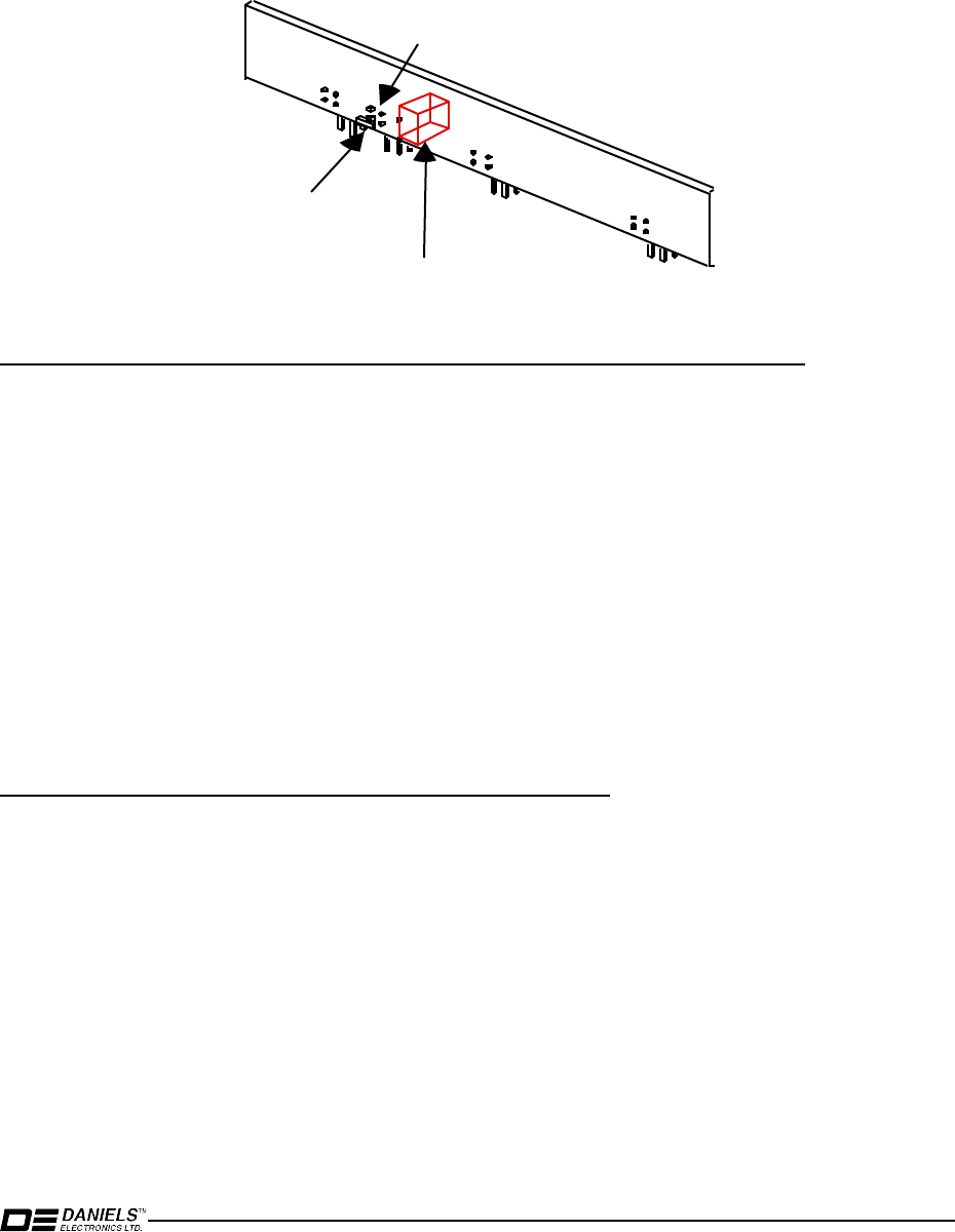
Transmitter Main Board Instruction Manual
3-13
input to the
transmitter
to be used to gain access to the SUBTONE INPUT 2
which
connects to the PHASE
MOD
IN input of a
modifi
ed synthesizer.
• Make sure J13 and J16 are not
installed.
Figure 3-1
Transmitter
Audio Processor Low Frequency
Modulation.
REMOVE
R47
REPLACE WITH
10 uF
+
SHORT TOP TWO PINS
MT3TXMNM7
MT-3
Transmitter
Audio Processor (board
version
43-911914 through 43-911916)
• Install jumpers:
JU38Y,
JU35Y
•
Remove
jumpers: JU27X,
JU27Y,
JU31, JU35X, JU37, JU38X
• Short pins P4-1 and P4-3 (or
install
J23)
together
with
a short
piece
of 22 or 24 gauge
solid
wire
and solder (see figure 3-1). This
allows
the DIRECT MODULATION input
to the
transmitter
to be used to gain access to the SUBTONE INPUT 2
which
connects to
the PHASE
MOD
IN input of a
modified
synthesizer.
Note that the SUBTONE 2 input should not be used
while
this
modification
is in
effect.
Note also
that
adjusting
R44 has no
effect
on the
deviation
of the low frequency signal.
MT-3
Transmitter
Audio Processor (board
version
43-911918)
•
Contact
factory for
configuration.
3.11.3
Synthesizer and Crystal Controlled Oscillator
Refer to the
manual
for the
Oscillator
used in your
Transmitter
for the required Low Frequency
Modulation
modifications.

3-14
Transmitter Main Board Instruction Manual
3.11.4
Tuning the Transmitter
For all MT-3
transmitters,
apply a low
impedance
source of 20-300 Hz to the Direct
Modulation
input of the
transmitter
(Pin Z28 of the 48 pin
connector)
through a 22 uF
capacitor,
posi
tive
terminal
connected
to pin Z28. A Marconi 2955 works
well
for this test.
Adjust
R44 on the audio
processor to the fully
clockwise
position.
• Apply a 100 Hz tone at -8 dBm to the Direct
Modulation
input of the
transmitter
(Pin Z28
of the 48 pin con
nector,
and key the
transmitter.
Adjust
the
level
of the tone
until
a
deviation
of 1.5 kHz is
acheived.
Note that the
level
required may be
anwhere
from -10
dBm to 0 dBm depending on the type of
transmitter.
• Confirm that the frequency response rolls off by
checking
that the
following
deviations
are
observed:
(note that the
deviation
will
NOT roll off at 300 Hz if an OC-3 crystal
oscillator
is used instead of a synthesizer).
- 20 Hz tone
gives
about 700 Hz
deviation
- 100 Hz tone
gives
1.5 kHz
deviation
- 300 Hz tone
gives
about 500 Hz
deviation
•
Finally,
confirm subtone 1
modulation:
set-up for 100 Hz Mod
with
500 Hz Dev.
- Check 200 Hz Mod, Dev = 1.5 (VHF) / 2.0 kHz
(UHF)
- Check 300 Hz Mod, Dev = 1.5 (VHF) / 4.0 kHz
(UHF)

Transmitter Main Board Instruction Manual
4-1
4
TRANSMITTER INTERCONNECT PIN DEFINITIONS
The MT-3 series
Transmitter
employs a 48 pin Eurostandard
connector
for
interfacing
to all
transmitter
power,
audio,
and control functions. The
following
are the MT-3 series
Transmitter
backplane
connections
to the M-3 Motherboard.
Pin
Name
Pin
Name
Pin
Name
D2 No Connect B2
+13.8
Vdc
Z2
+13.8
Vdc
D4 No Connect B4 MIC Out Z4 MIC In
D6 No Connect B6
+9.5
Vdc
Z6
+9.5
Vdc
D8 No Connect B8 Relay Positive Z8 Relay
Negative
D10 No Connect
B10
PTT WTO
Z10
PTT WTO
D12 No Connect
B12
Tx Standby
Z12
Tx Standby
D14 No Connect (IMC1)
B14
PTT NTO
Z14
PTT NTO
D16 No Connect (IMC2)
B16
No Connect (MT-2 +9.5V)
Z16
No Connect (MT-2 +9.5V)
D18 No Connect (IMC3)
B18
Balanced
Input 2
Z18
Balanced
Input 1
D20 Channel Select 0 (LSB)
B20
Squelched,De-emph
Audio
Z20
Squelched,
Flat Audio
D22 Channel Select 1
B22
Subtone Input 1
Z22
Tx Audio Control
D24 Channel Select 2
B24
PTT Output
Z24
Subtone Input 2
D26 Channel Select 3 (MSB)
B26
Forward
Power Sense
Z26
Reverse Power Sense
D28
Synth
Tx Data (Output)
B28
Monitor Out
Z28
Direct Mod Input
D30
Synth
Rx Data (Input)
B30
Ground
Z30
Ground
D32
Synth
Bootstrap (Input)
B32
Ground
Z32
Ground

4-2
Transmitter Main Board Instru
ction Manual
This Page Intentionally Left Blank
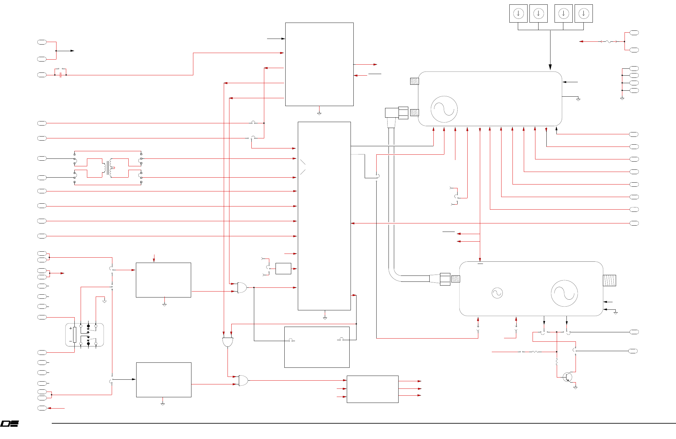
LED ENA
X
X
X
Y
Y
Y
Y
X
X
Y
B20
J16
RELAY1
J2
12
13
11
U2d
U2c
D32
D20
+9.5VDC
+9.5 VDC
2
13
U2a
J17
JP1-2
+9.5 VDC
Z20
B4
Z4
B22
Z18
B18
Z24
Z28
B12
Z12
B10
Z10
B14
Z14
B24
D12
D2
B8
Z8
D8
D10 J1
D30
D28
D22
D24
D26
Z22
B26
Z26
Z30
Z32
B30
D6
D4 Y
X
J4
X
Y
+9.5V
+9.5V OUTPUT
GROUND
MIC PTT WTO
MIC PTT NTO
MIC AUDIO
MT-3 FRONT PANEL BOARD
RX AUDIO / +13.8V
B2
Z2
+13.8VDC
B6
Z6
RF OUT
REFERENCE
INPUT OS-3 SYNTHESIZER MODULE
R
FRONT PANEL
N CONNECTO
RF IN RF OUT
+9.5V
+13.8V
FOR REV
ENA
MT-3 VHF/UHF AMPLIFIER MODULE
OR
LED ENA
+9.5VDC
PTT TRIGGER
PTT WTO
TRIGGER
+9.5VDC
SWITCHING
CIRCUITRY
+9.5VDC
VSWR REVERSE
FORWARD POWER FAIL
INDICATOR
10-17 VOLTS
+ 13.8 VDC NOMINAL
BACKPLANE
CONNECTOR
GROUND
GROUND
GROUND
GROUND
RX DATA IN
TX DATA OUT
BOOTSTRAP
CHANNEL SEL 0 (LSB)
CHANNEL SEL 1
CHANNEL SEL 2
CHANNEL SEL 3 (MSB)
TX AUDIO CONTROL
+9.5 VDC PTT SWITCHED
J12
R25
27K4 R26
1K0
Q10
PZT2222A
J14
J15J13
FUSE
(OPTIONAL)
+9.5 VDC CONTINUOUS
J9
SQL DE-EMP INPUT
MIC OUT
MIC IN
BALANCED INPUT
SIDE 2
600 OHMS
BALANCED INPUT
SIDE 1
SUBTONE
INPUT #1
SUBTONE
INPUT #2
SQL FLAT
INPUT
DIRECT MOD
INPUT
PTT WTO
TX
STANDBY
NO2
COMMON 2
NC2
RLY POS
RLY NEG
NC 2
NC 1
COMMON 1
PTT NTO
PTT OUTPUT PTT OUTPUT
TX STANDBY
PTT
+ 9.5 VDC PTT SWITCHED
+ 9.5 VDC SWITCHED
J3
Y
X
J7
+ 9.5 VDC PTT
SWITCHED
+ 9.5 VDC
SWITCHED
8
10
9
1 7 9 8
10 4 2 3
01
2
3
4
5
6
7
8
901
2
3
4
5
6
7
8
901
2
3
4
5
6
7
8
901
2
3
4
5
6
7
8
9
MSB LSB
T1
600Ω
PTT
Y
X
J18
+ 9.5 VDC PTT
SWITCHED
+ 9.5 VDC
SWITCHED
PTT OUTPUT
8 VDC
SUPPLY
+9.5 VDC
Y
X
Y
X
Y
X
Y
X
J20
J22
J23
J19
AUDIO OUTPUT
SUBTONE #2 OUTPUT
MICROPHONE
INPUT
BALANCED INPUT
+9.5V
+8.0V SWITCHED
TONE/DIGITAL INPUT
SUBTONE #1 INPUT
SUBTONE #2 INPUT
DIRECT MODULATION INPUT
GND
MT-3 AUDIO
PROCESSOR
AUDIO CONTROL
AM(N/C)
AM(N/C)
AM(N/C)
AM(N/C)
AM(N/C)
AM(N/C)
TOT INPUT
TOT OUTPUT
J35
J33
TOT INPUT TOT OUTPUT
TIME OUT TIMER
Y
X
J25
JP1-7
B32
ELECTRONICS LTD.
DANIELS TM
MT-3 AM Transmitter Main Board Instruction Manual
5 ILLUSTRATIONS AND SCHEMATIC DIAGRAMS
5.1 Transmitter Block Diagram
5-1
MT3TXMNM1D

DE
DANIELS
ELECTRONICS
5-2
Transmitter Main Board Instruction Manual
This Page Intentionally Left Blank
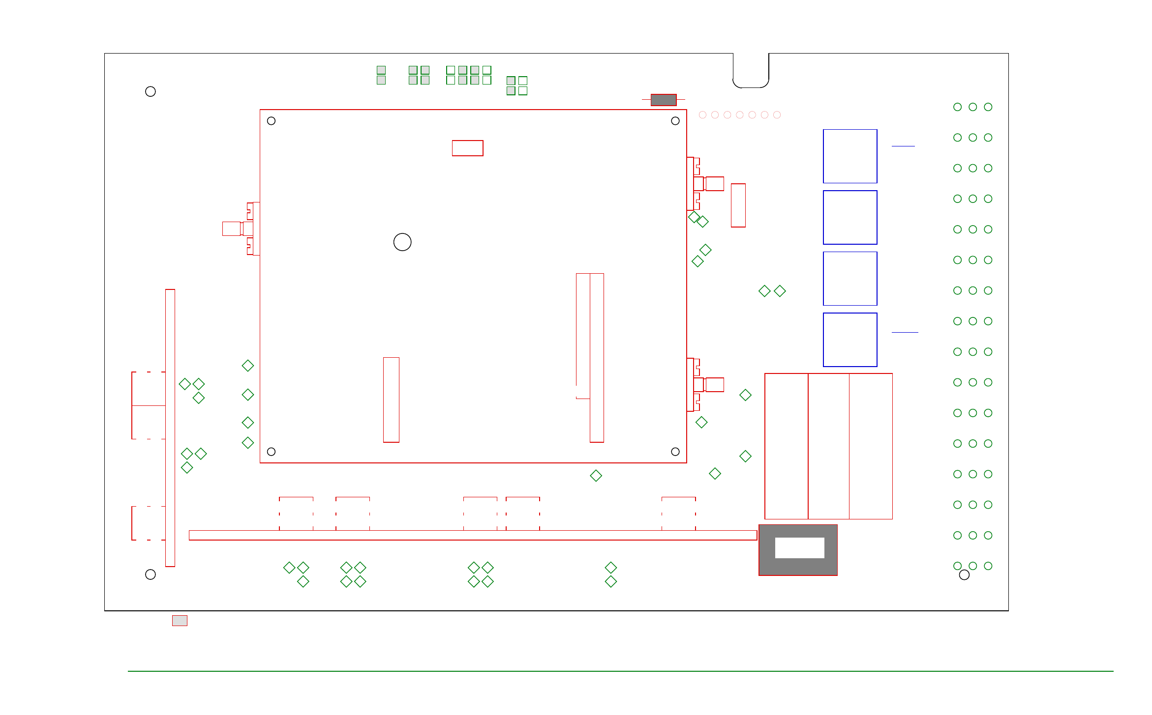
VICTORIA B.C .
DATE:
May 9, 1997
D
DANIELS
ELECTRONICS
BOARD No.:
43-920917
DWG REV DATE:
43-920917
DWG No:
9209AS3A
TITLE:
MT-3 Component Side SM Layout
Factory installed jumpers
DWG No:
9209AS4A
TITLE
:
MT-3 Transmitter Component Side SM Designations
J27
J26
J29
J28
J32
J31
J35
J33
J34
20
19
18
17
16
15
14
13
T1
SPT-196
JS3
JS2
JS1
6
5
4
3
2
1
1
2
MT-3 FRONT PANEL BOARD
12
11
10
9
8
7
6
5
4
3
2
1
1R0W X 12PIN
1ROW X 9PIN
1ROW X 6PIN
1ROW X 2PIN
RELAY1
OPTIONAL
MT-3 AUDIO PROCESSOR BOARD
3
4
1
2
3
4
1
2
3
4
1
2
3
4
1
2
3
4
1
2
JA1
JA2
JA3
JA4
JA5
3
4
1
2
1
2
JF1
JF2
ENA
+9.5V
13.8V
FOR
REV
GND
DWG No:
TX3AT9D
TITLE:
MT-3 Transmitter Component Side T/H Designations
DWG REV DATE:
3
4
JF3
AUDIO IN
C23
100nF
R42
OPT
FSW4
BCD-10
FSW3
BCD-10
FSW2
BCD-10
FSW1
BCD-10
MSD
LSD
- Components Not Installed
12B
SYNTHESIZER GROUND TAB
(Low Power Synthesizer Only)
SYNTHESIZER
GROUND TAB
(Low Power
Synthesizer
Only)
OS-3 RF
OUTPUT
OC-3 RF
OUTPUT
OS-3H ENHANCED SYNTHESIZER
OR
OC-3 CRYSTAL CONTROL MODULE
OST-3H RF
OUTPUT
TP19
TP20
TP22
TP21
32
30
28
26
24
22
20
18
16
14
12
10
8
6
4
2
D
B
Z
TP15
TP16
TP18
TP17
TP12
TP13
TP14
TP1
TP2
TP3
TP4
TP5
TP6
TP8
TP9
TP10
TP11
TP7
TP25
TP26
TP27
TP28
TP29
TP30
TP24
TP23
TP33
TP34
TP31
TP32
DE
DANIELS
ELECTRONICS
5-5
Illustrations and Schematic Diagrams
MT3TXMNM2B
Factory installed jumpers
5.2
MT-3 AM Transmitter Board Electrical Assembly
5.2.1
MT-3 AM Transmitter Board Component Layout (Top)
DE
DANIELS
ELECTRONICS
5-3
MT-3 AM Transmitter Main Board Instruction Manual
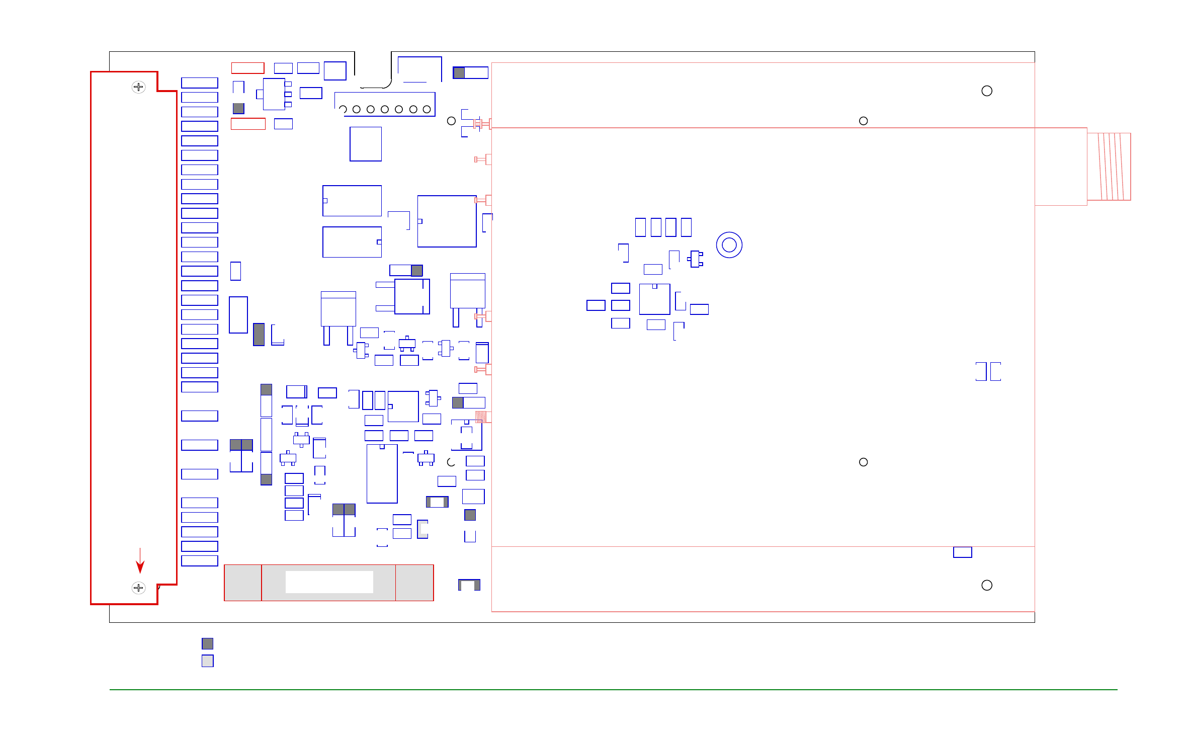
VICTORIA B.C .
DATE.:
9 May 1997
D
DANIELS
ELECTRONICS
BOARD No.:
43-920917
43-920917
+
+
+
+
+
TITLE:
MT-3 Transmitter Solder Side SM Layout
DWG No:
9209AS3B
DWG REV DATE:
10 Aug. 1998
+
Factory installed jumpers
Components Not Installed
TITLE:
MT-3 Transmitter Solder Side SM Designations
DWG No:
9209AS2D
J18
BYD17J
D4
R2 27k4
D2
BYD17J
R9 221k
R10
100k
R3
1k00
D1
BYD
17J
D3
BYD
17J
R6
27k4
R7
1k00
R8
27k4
C6
10nF
C5
100nF
U1
33172
10nF C7
100nF C8
R4
27k4
R15
10k0
R18
10k0
U2
4081
R14
10k0
Q1
BC817
BC817
Q3
R12
27k4
R13
27k4
R11
27k4
D6
BYD17J
C3 16V
10µF
C4
1µF
16V
Q9
D15N
06V
Q8
BC807
R24
68k1
R22
68k1
R23
10k0
R21
10K0
R19
10k0
Q4
BC817
R20
68k1
D5
BYD
17J
Q5
D5P06V
Q7
D5P06V
U3
MMAD1108
U4
MMAD1108
C1
10µF
35V
R26
1k00
Q10
PZT
2222
R25
27k4
C2
1µF
35V
Q6
BC817
y
J4
x
J9
J17
y
x
J12
J6
R17
1k00
C12
10nF
C13
10nF
LPF35
LPF34
LPF33
LPF32
LPF31
LPF30
LPF29
LPF28
LPF27
LPF26
LPF25
LPF24
LPF23
LPF22
LPF21
LPF20
LPF19
LPF18
LPF17
LPF16
LPF15
LPF12
LPF10
LPF8
LPF3
LPF5
LPF4
LPF2
LPF1
D8
BAS
16
y
J3
x
y
J2
x
x
y
J21
U6
LP
2951
y J7 x
J14
y
R29 82k5
x J13 y
R5
10R0
J16
R110R0
R30
15k0
C15
4.7µF
C14
10nF
D7
BAS
16
M2.5 PRESS NUT
x
LPF14
C10
1 µF
y J25 x
R16
10k0
x
y
x
y
J20
J23
x
y
J19
J22
J24
x J15 y
C20
4.7µF
16V
U8
MC14536B
R39
221K
U7
33172
R32
1k00
R34
27k4
R33
68k1
R31
221k
R38
100k
R37
1k00
R36
221k
R35
27k4
C21
100nF
C22
100nF
R47
1k00
Q11
BC807-25
R46
221k
R43
221k
R44
221k
R45
221k
R41
15K
R40
10K
x
y
R28
DWG REV DATE:
10 Aug. 1998
F1
(3A FUSE OPTIONAL)
CONN1
F/48 MALE
TITLE:
MT-3 Transmitter Solder Side T/H Designations
DWG No:
TX3AT8D
DWG REV DATE:
10 Aug. 1998
M2.5 x 10
PAN/PHIL.
SCREW (2)
Components Not Installed
MT-3 AM AMPLIFIER
GND: BLACK
+ 13.8 VDC: RED
MODULATION INPUT: YELLOW
ENA: BLUE
+ 9.5 VDC: ORANGE
RF IN
BLK
YEL
RED
BLUE
1
2
3
4
5
6
ORG
7
5-4
MT-3 AM Transmitter Main Board Instruction Manual
DE
DANIELS
ELECTRONICS
5.2.2
MT-3 AM Transmitter Main Board Component Layout (Bottom)
MT3TXMNM3B
x J15 y
x J13 y
J6
y J25 x
y J7 x
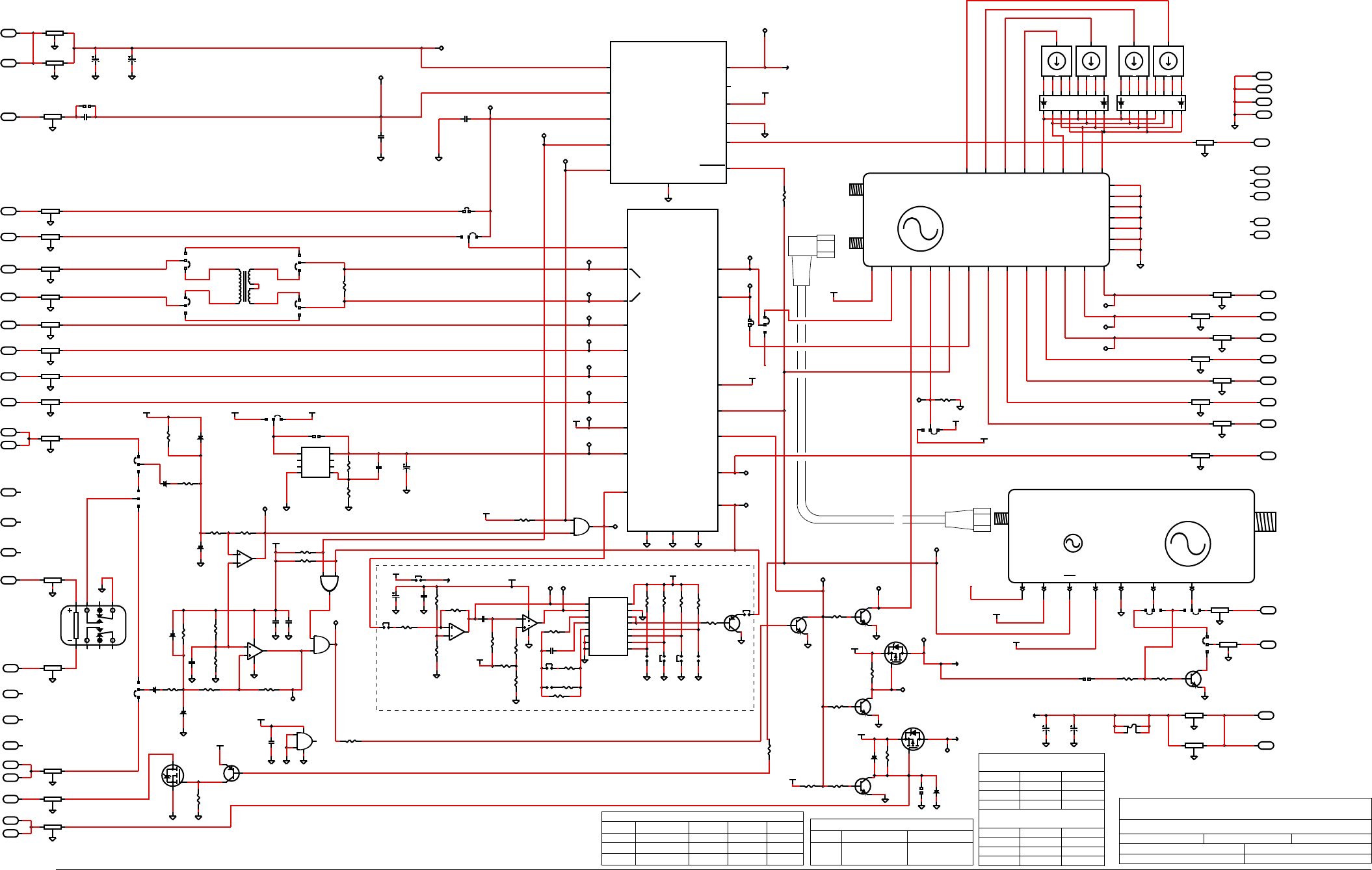
DANIELS
DE
ELECTRONICS
J6
J7
InstalledNot Installed
'Y' Position
'X' PositionJ18
Installed Installed
'Y' Position
'X' Position
'X' Position
'X' Position
MODE 1 MODE 2 MODE 3 MODE 4
AM/FM STANDBY MODES
STANDARD/LOW FREQUENCY MODULATION
STD MOD VER. LF MOD VER.DESIGN
J6
J7
J18
Installed
'X' Position
'X' Position
Not Installed
'Y' Position
'Y' Position
VICTORIA B.C.
DE
DANIELS
ELECTRONICS
Transmitter Main Board Instruction Manual 5-5
5.2.3 Transmitter Main Board Schematic Diagram
D
W
G RE
V
DATE: 9 O
C
TOBER 1998
D
W
G No.:
M
T3TX
M
N
M
4B
Y
X
N
C
N
C
N
C
M M M
M
L L L
X
BOARD RE
V
: 1.7 BOARD No.: 43-920917
TP34
C
23
C
17-
C
19 LPF6,LPF7 LPF11,LPF13
Q2
C
9,
C
11,
C
16
Q11
R47
U8
J35
U5R27
J10,J11
J1,J5,J8
FS
W
4
F1
RELA
Y
1
H
I
GHEST REFEREN
C
E DES
I
GNATORS
LPF35
T1
D8
----- ----- -----
UNUSED REFEREN
C
E DES
I
GNATORS
TIME OUT TIMER
APPROX 0.8 VDC
JF3-4
JF3-3
JF3-2
JF3-1
TO
J25 PIN3
TO
JP1-7
X
Y
X
Y
X
Y
X
Y
X
Y
JP1-5JP1-4JP1-6JP1-2JP1-1JP1-3
XY
Y
X
Y
XYX
Y
UNDER U6
X
Y
X
Y
XY
T
I
TLE:
M
T-3 TRANS
M
I
TTER BOARD S
C
HE
M
AT
I
C
D
I
AGRA
M
JA5-1
JA5-2
JA5-3
JA5-4
JA2-4
JA3-1
JA4-2
JA3-2
JA4-4
JA1-4 JA3-3
JF2-3
JF2-4
JF1-4
JA3-4
JA2-3
JA4-3
JA4-1
JA2-1
JA2-2
JA1-1
JA1-2
JA1-3
APR
V
D:D
W
G B
Y
:
M
I
KE GAUBE DATE: 8 APR
I
L 1992
JF1-1
JF1-3
JF2-2
JF1-2
JF2-1
FRONT PANEL
N
C
ONNE
C
TOR
BA
C
KPLANE
C
ONNE
C
TOR
LPF
LPF16
LPF
LPF17
LPF
LPF22
LPF
LPF5
LPF
LPF4
LPF
LPF19
LPF
LPF18
LPF
LPF20
LPF
LPF27
LPF
LPF21
LPF
LPF33
LPF
LPF12
LPF
LPF8
LPF
LPF10
LPF
LPF14
LPF
LPF26
LPF
LPF15
Z12
TX STANDBY
B12
PTT OUTPUT
B24
Z14
PTT NTO
B14
NCD4
NCD6
NC
D2
RLY POS
B8
NC
D8
NC
D10
NCD12
Z10
PTT WTO
B10
DIRECT MOD
INPUT
Z28
SQL FLAT
INPUT
Z20
SUBTONE
INPUT #2
Z24
SUBTONE
INPUT #1
B22
BALANCED
INPUT #1
Z18
BALANCED
INPUT #2
B18
MIC IN
Z4
MIC OUT
B4
SQL DE-EMP
INPUT
B20
Z6
+9.5V CONTINUOUS
B6
GROUND
B30
GROUND
B32
GROUND
Z32
IMC1
D14
IMC2
D16
IMC3
D18
NC B16
NC Z16
RX MONITOR
B28
RX DATA IN
D30
TX DATA OUT
D28
BOOTSTRAP
D32
CHANNEL SEL 0
(Least Significant Bit)
D20
CHANNEL SEL 1
D22
CHANNEL SEL 2
D24
CHANNEL SEL 3
(Most Significant Bit)
D26
TX AUDIO CONTROL
Z22
VSWR REVERSE
Z26
FORWARD POWER
FAIL INDICATOR
B26
+10 TO +17 VOLTS
+13.8 VDC NOMINAL
B2
Z2
LPF
LPF2
LPF
LPF1
LPF
LPF34
LPF
LPF35
LPF
LPF23
LPF
LPF29
LPF
LPF28
LPF
LPF25
LPF
LPF24
LPF
LPF32
LPF
LPF31
LPF
LPF30
10uF
C3
1.0uF
C4
TP5
TP2
TP4
TP3
TP1
10nF
C13
TP6
TO ALL 9.5V SUPPLY POINTS
1.0uF
C10
J9
J16
J17
TP20
TP18
TP22
TP17
TP19
TP21
NOT INSTALLED
R28
9.5V
27K4
R2 BYD17J
D2
BYD17J
D1
J3
1 9 87
4 3210
RELAY1
J4
BAS16
D7 10R0
R1
27K4
R4
1K0
R3
TP27
2
31
MC33172
a
U1
4
5
67
8
MC33172
b
U1
BYD17J
D3
27K4
R6
BYD17J
D4
BAS16
D8
10R0
R5 1K0
R7
27K4
R8
TP28
10nF
C6
100K0
R10
221K0
R9
9.5V
9.5V
TP26
8 9
10
MC14081
c
U2
13
12
11
MC14081
d
U2
100nF
C8
9.5V
5
6
4
14
7
MC14081
b
U2
1
2
3
MC14081
a
U2
9.5V
G
D
S
D15N06V
Q9
E
B
C
BC807-25
Q8
10K0
R18
TP11
E
B
C
BC817-25
Q1
E
B
C
BC817-25
Q3
9.5V
9.5V
E
B
C
BC817-25
Q4
BYD17J
D5
BYD17J
D6
J6
TP7
G
DS
D5P06V
Q5
J21
Vin
Error
Sd
Gnd
Vout
Sense
5V Tap
FB
8
5
3
4
1
2
6
7
LP2951
U6
15K0
R30
9.5V
10nF
C14
82K5
R29
4.7uF
C15
J15J13
J14
E
B
C
PZT2222A
Q10
1K0
R26
27K4
R25
J12
9.5V
TO ALL 13.8V SUPPLY POINTS
13.8V
10uF
C1
1.0uF
C2
TP8
TP15
13.8V
TP9
TP16
TP14
1K0
R17
J18
10K0
R16
TP23
TP24
TP10
9.5V
9.5V SWITCHED
J7
TO ALL 9.5V SWITCHED
SUPPLY POINTS
TO ALL 9.5V PTT SWITCHED
SUPPLY POINTS
9.5V PTT SWITCHED
9.5V PTT SWITCHED
MICROPHONE INPUT
BALANCED
INPUT
+9.5V
+8.0V SWITCHED
TONE/DIGITAL
INPUT
AUDIO OUTPUT
SUBTONE #1 INPUT
SUBTONE #2 INPUT
DIRECT MODULATION
INPUT
AUDIO
SUBTONE #2
OUTPUT
TOT
INPUT TOT
OUTPUT
GND GND
MT-3 AUDIO
PROCESSOR
13.8 V
QUALIFIED
PTT
PTT
GND
CONTROL
2
1
6
4
5
3
AUDIO XFMR
T1
10nF
C12
27K4
R13
27K4
R12
27K4
R11
10K0
R19
10K0
R15
1 2
10K0
R14
68K1
R20
10K0
R23
68K1
R24
100nF
C5
10nF
C7
J20
J22
J23
J24
J19
J25
+9.5V INPUT
+9.5V OUTPUT
LED ENA
GROUND
MIC PTT WTO
MIC PTT NTO
MIC AUDIO
MT-3 FRONT PANEL BOARD
RX AUDIO
SPARE
+13.8V
GROUND
RX MON
13.8V
RF IN RF OUT
+9.5V+13.8V ENA GND FOR REV
OR
MT-3 VHF/UHF AMPLIFIER MODULE
AUDIO
IN
XXXX
LPF
LPF3
F1
OPTIONAL
RLY NEG
Z8
68K1
R22
9.5V
E
B
C
BC817-25
Q6
TP30
TP29
G
DS
D5P06V
Q7
10K0
R21
100nF
C22
221k
R39
C23
100nF
221k
R44
221k
R45
221k
R46
221k
R43
15k0
R41
27k4
R35
68k1
R33
221k
R31
1k00
R32
221k
R36
27k4
R34
100k
R38
1k00
R37
OPT
R42
J26
J27
J32
J28
100nF
C21
3
28
4
1
a
MC33172
U7
Q11
BC807-25
SET
RESET
IN1
OUT1
OUT2
BYP
CLK INH
VSS
VDD
MONO
OSC INH
DEC
D
C
B
A
MC14536B
1
2
3
4
5
6
7
8
16
15
14
13
12
11
10
9
U8
TP25
5
67
MC33172
U7
b
9.5V
4.7uF
C20
1k00
R47
10k0
R40
J29 J31
J35
J33
J34
TO ALL TOT 9.5V
TOT 9.5V
TOT 9.5V
TOT 9.5V
TP12
TP31 TP32
TP13
TP33
TP34
GROUND
Z30
OC-3 CRYSTAL CONTROL MODULE
P1-18 P1-20 P1-12 P1-19 P1-11 P2-2 P1-17 P1-9
P3-2
P3-1
P2-5
P1-10
P1-7
P1-3
P2-3
P1-16P1-8P1-15P1-14P1-6P1-13P1-5P1-4
P1-2 P1-1 P2-1 P2-4 P2-6
RF
OUTPUT
REFERENCE
INPUT
OS-3 SYNTHESIZER
OR
012
3
4
5
6
7
89
MSD
FSW1
13572468
9 11 13 15 10 12 14 16
U3
MMAD1108
75318642
15 13 11 9 16 14 12 10
U4
MMAD1108
012
3
4
5
6
7
89
FSW2
012
3
4
5
6
7
89
FSW3
012
3
4
5
6
7
89
LSD
FSW4
9.5V SWITCHED
J2
PTT
TOT INPUT
TOT OUTPUT
QUALIFIED PTT
QUALIFIED PTT
JP1-7
JP1-7
2.2 Vdc
9.4Vdc
2.9 Vdc
2.9Vdc
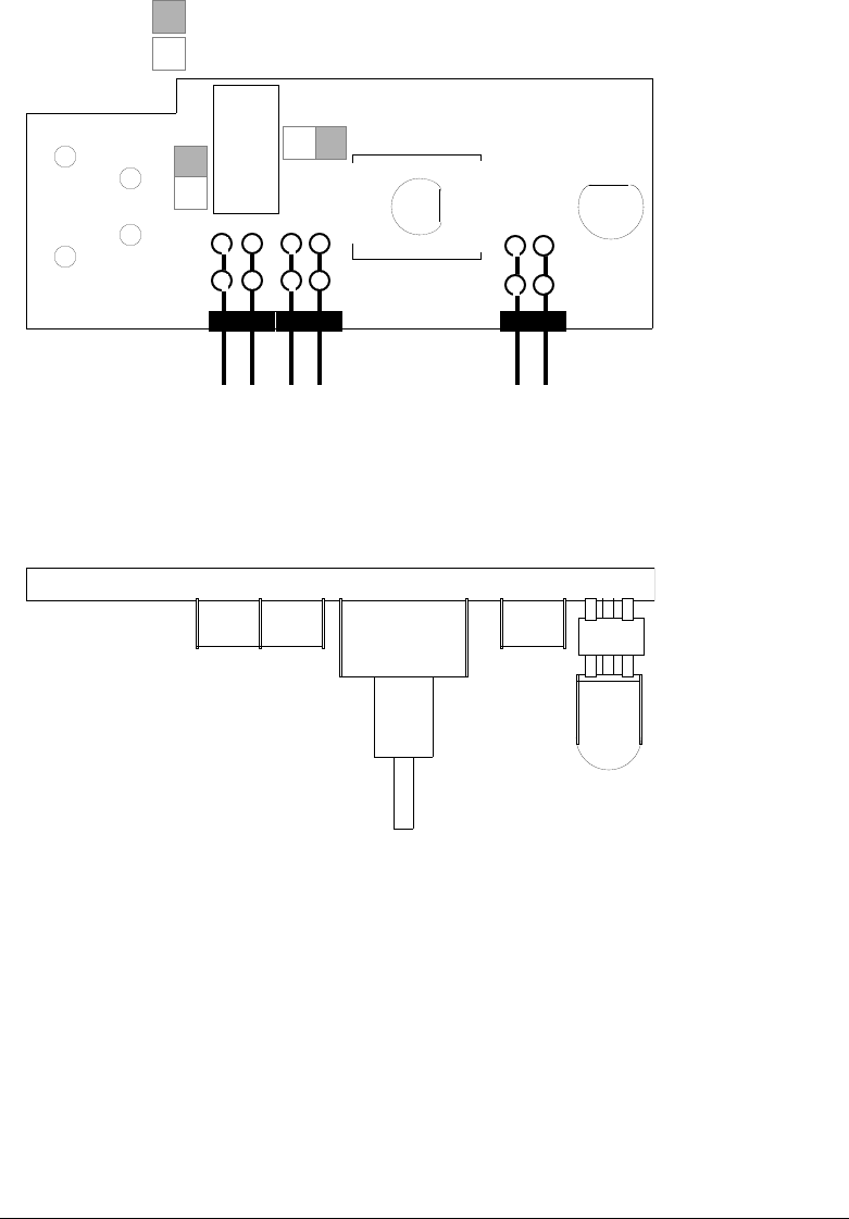
DE
DANIELS
ELECTRONICS
5-6
Transmitter Main Board Instruction Manual
5.3
Front Panel Board
5.3.1
Front Panel Board Component Layout
D1
MIC
1
2
3
4
PF2
SW1
PF1
+
c b a
f e d
KEYED
NORM
J1
Y
X
Solder Jumper On Solder Side Of PCB.
Factory Installed Solder Jumper.
MT3TXMNM5A
PF3
J2
Y
X
43-921212
P1
2
1
4
3
6
5
8
7
1
2
3
4
1
2
3
4
1
2
3
4
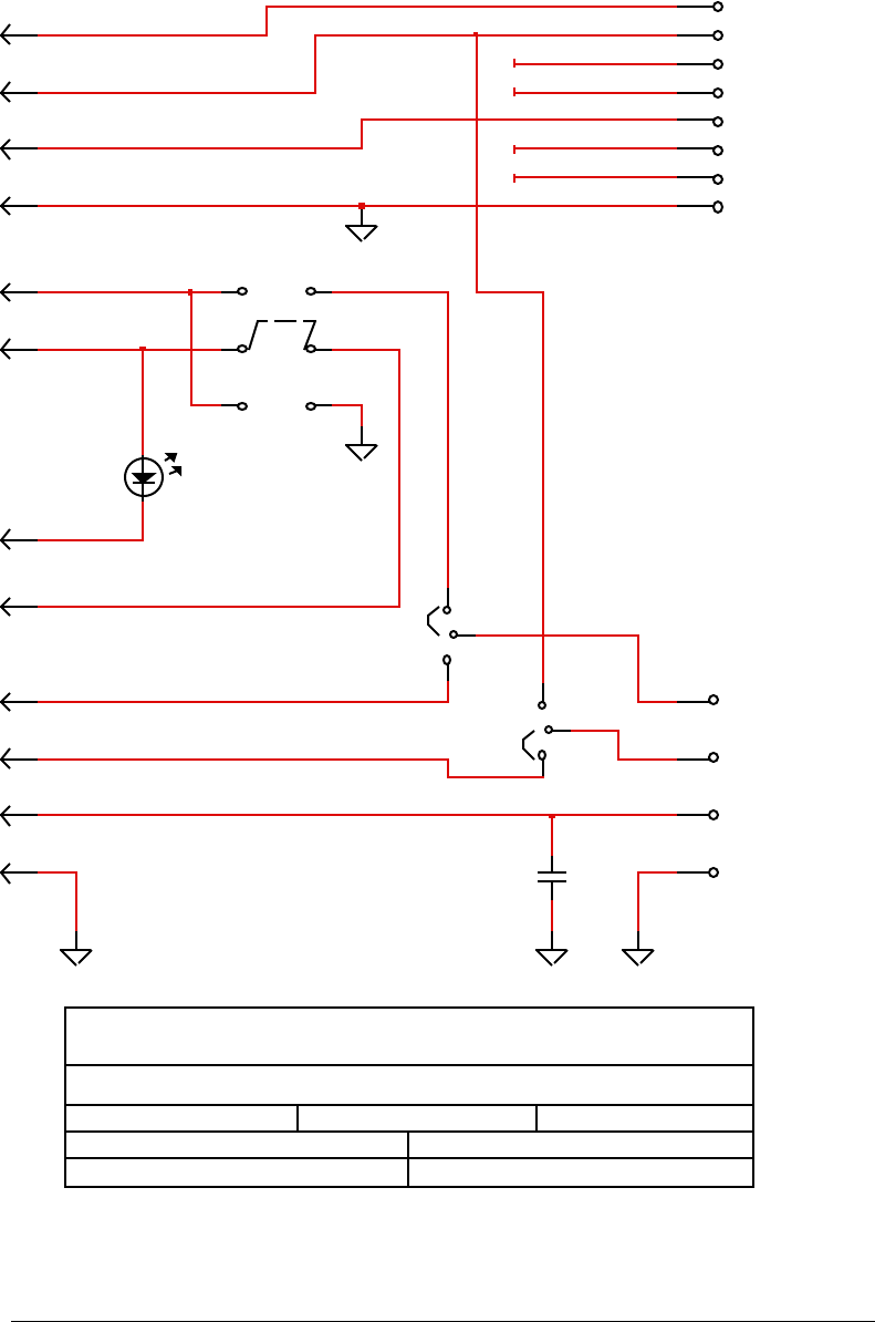
DE
DANIELS
ELECTRONICS
Transmitter Main Board Instruction Manual
5-7
5.3.2
Front Panel Board Schematic Diagram
VICTORIA B.C .
DATE.:
DWN:
DWG No:
TITLE:
APRVD:
BOARD NO.:
BOARD REV.:
DWG REV DATE:
DE
DANIELS
ELECTRONICS
NORM
KEYED
Y
M
IC-1
M
IC-3
M
IC-4
M
IC-2
PF2-1
PF2-4
PF2-3
PF2-2
PF1-3
PF1-2
PF1-1
PF1-4
X
M. GAUBE
MT
-
3 FRONT PANEL BOA
R
D
43-921212 1.2
PF3-2
PF3-1
PF3-4
PF3-3
Y
X
07 APRIL 1992
28 MAY 97
MT3TXMNM6A
D1
J1
N/I
C1 1
2
3
4
MIC
1
2
3
4
PF1
PF2
4
2
1
3
PF3
1
2
3
4
5
6
7
8
P1
J2
F
E
D
C
B
A
SW1
+9.5V IN
LED ENA
MIC PTT NTO
MIC PTT WTO
MIC INPUT
MIC INPUT
MIC PTT
MIC PTT
RX MON
RX MON
+9.5V OUT
+9.5V OUT
RX AUDIO
RX AUDIO
+13.8V
+13.8V
SPARE
SPARE
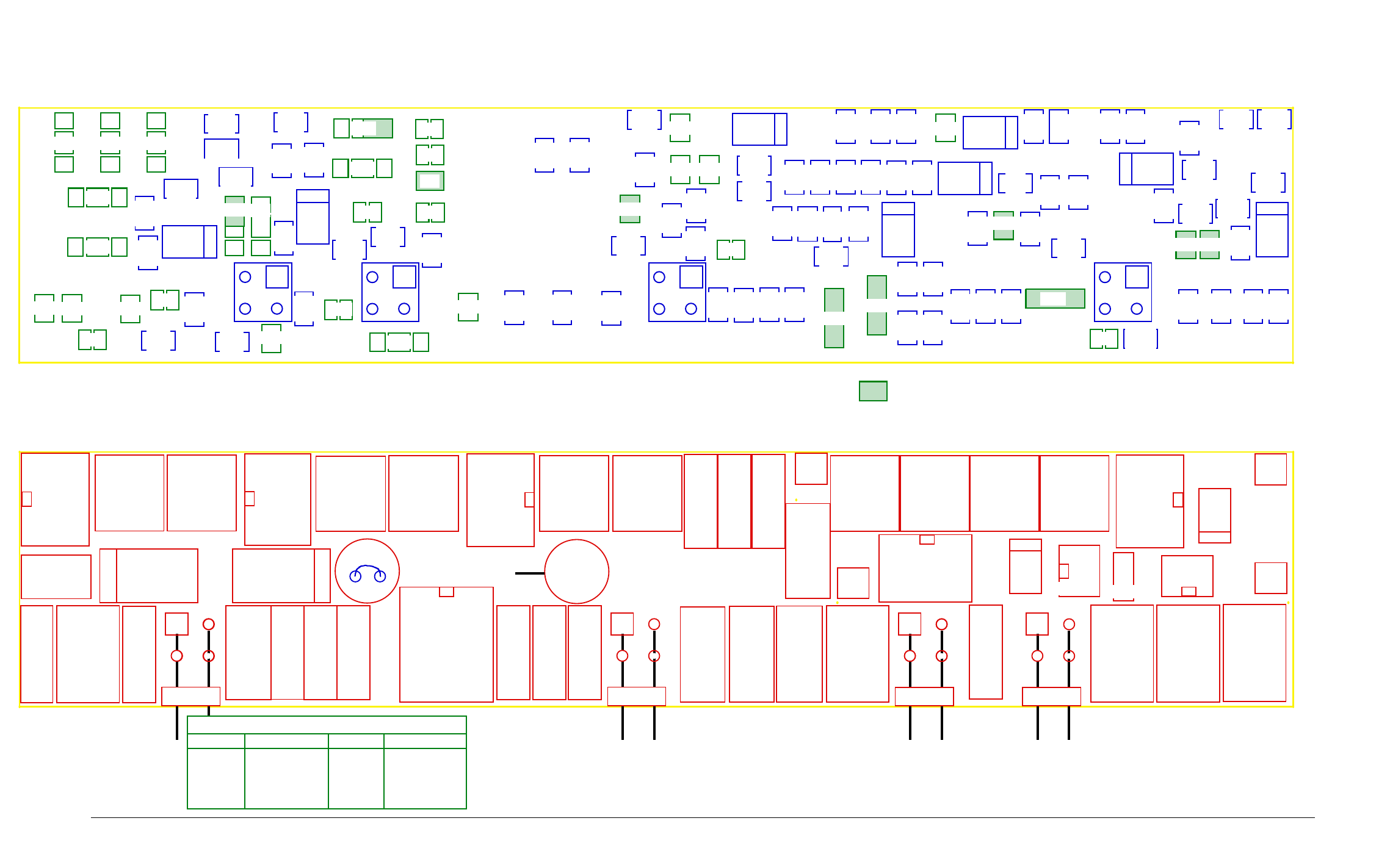
DWG No:
TXADPROAS
TITLE:
MT-3 Tx Audio Processor
VICTORIA B.C .
D
DANIELS
ELECTRONICS LTD.
DATE:
19 April, 1996
BOARD No.:
43-911916
REV DATE: 22 August, 1996
43-911916
DWG No: TX ADPROAS
TITLE: MT-3 Tx Audio Processor
DWG No:
TXADPROAS1A
TITLE:
MT-3 Tx Audio Processor SM Layout
INSTALL JUMPERS
U1
SL6270
R2
5k POT
MICROPHONE
INPUT LEVEL
CONTROL
R8
100k POT
MICROPHONE
COMPRESSION
CONTROL
U2
SL6270
R31
5k POT
BALANCE
INPUT LEVEL
CONTROL
R38
100k POT
BALANCED
COMPRESSION
CONTROL
FB1
Ferrite Bead
U5
MC33174
U3
MC33172
R42
5k POT
SUBTONE
INPUT 1
CONTROL
LEVEL
R29
50k POT
DEVIATION
CONTROL
U4
MC33172
R75
50k POT
DC LEVEL
ADJUST
R44
5k POT
SUBTONE
INPUT 2
CONTROL
LEVEL
U8
MC33172
C55
4.7µF
U10
TC4S66F
Q2
TC4S66F
C56
4.7µF
R48
100K POT
AUXILIARY
INPUT LEVEL
CONTROL
R14
50k POT
SYMMETRY
ADJUST
R82
27k4
C7
10nF
R6
1k00
C10
2.2µF
R5
1k00
C11
150pF
R35
1k00
JU3
C4
100nF
R1
604R
R7
20k0
R3
6k81
C6
10nF
R83
27k4
R36
1k00
R37
20k0
C33
6.8µF
R4
221k
R34
221k
C5
10nF
JU4
C34
150pF
JU5
R33
1k50
C30
4.7µF
JU11
C28
100nF
R32
1k5
R18
1k
R20
1k82
R85
39k2
JU24
R84
39k2
R23
5k11
R24
5k11
R25
3k48
R26
3k48
R86
22k1
R87
22k1
C29
4.7µF
JU25
JU26
R9
221k
C13
10pF
R12
11k8
C15
10nF
R11
49k9
R10
49k9
C14
100nF
C36
10pF
C54
4.7µF
C20
100nF
R21
49k9
R22
49k9
C53
10nF
R17
4k53
R89
100k
R28
13k3
R27
13k3
R30
681R
C3
4.7µF
R39
221k
R88
100k
JU2
JU23
JU12
JU13
R15
49k9
C17
10nF
R80
68k1
R13
49k9
R51
1k50
JU6
R50
221k
R49
27k4
R41
11k8
R52
11k8
JU29
JU14
JU10
JU9
JU15
C19
150pF
JU27
JU36
JU16
JU7
R16
100k
R47
4k53
JU39
C49
10nF
C52
4.7µF
C18
100nF
R43
11k8
JU1
R74
27k4
C50
4.7µF
JU38
JU30
JU35
JU34
JU28
C51
100nF
R79
49k9
R77
20k0
R78
49K9
JU37
R45
39k2
JU31
JU8
JU33
JU32
R73
221k
R72
39k2
C58
150pF
R61
221k
R71
63k4
R46
4k53
R40
1k50
Y
X
X
Y
X
Y
Y
X
X
Y
X
Y
Y
X
X
Y
Y
X
BC817-25
U9
DWG No:
TXADPROAS3B
TITLE:
MT-3 Tx Audio Processor SM Value / Designation
C8
47µF
C31
47µF
JU18
JU19
Y
X
R90
10k
JU17
REV DATE: 30 October 1996
P5-1
P7-1
P6-1
P8-1
C9
100nF
C12
680nF
C32
4.7nF
C22
10nF
C21
10nF
C24
10nF
C26
1nF
C25
15nF
C23
22nF
R81
10k
THERM.
C16
4.7nF
C37
4.7nF
C43
4.7nF
C41
150nF
C38
330nF
C44
330nF
C48
1µF
C39
330nF
C27
33nF
C57
1µF
C40
1µF
C47
1µF
P1
P2
P4
P3
1
2
3
4
1
2
3
4
1
2
3
4
1
2
3
4
1
2
3
4
1
2
3
4
1
2
3
4
1
2
3
4
TITLE:
MT-3 TX Audio Processor T/H Layout (Standard Version)
DWG REV DATE:
DWG No:
VUAP3AT1D
P1
P2
P4
P3
C35
330nF
DWG REV DATE:
2 September 1997
R19
DE
DANIELS
ELECTRONICS
MT-3 Transmitter Instruction Manual
5.5
MT-3 Audio Processor Electrical Assembly- PCB No. 43-911916
5.5.1
MT-3 Audio Processor Component Layout
Figure 5-9
MT-3 Audio Processor Component Layout
5-8
Low Frequency Modulation Configuration
Desig
Low Freq.
JU27X
JU27Y
JU31
JU35X
Not Installed
Not Installed
Not Installed
Not Installed
JU35Y
JU37
JU38X
JU38Y
Installed
Not Installed
Not Installed
Installed
Desig
Low Freq.
NOTE: For Low Frequency Modulation
short pins P4-1 and P4-3 together.
MT3APM1A
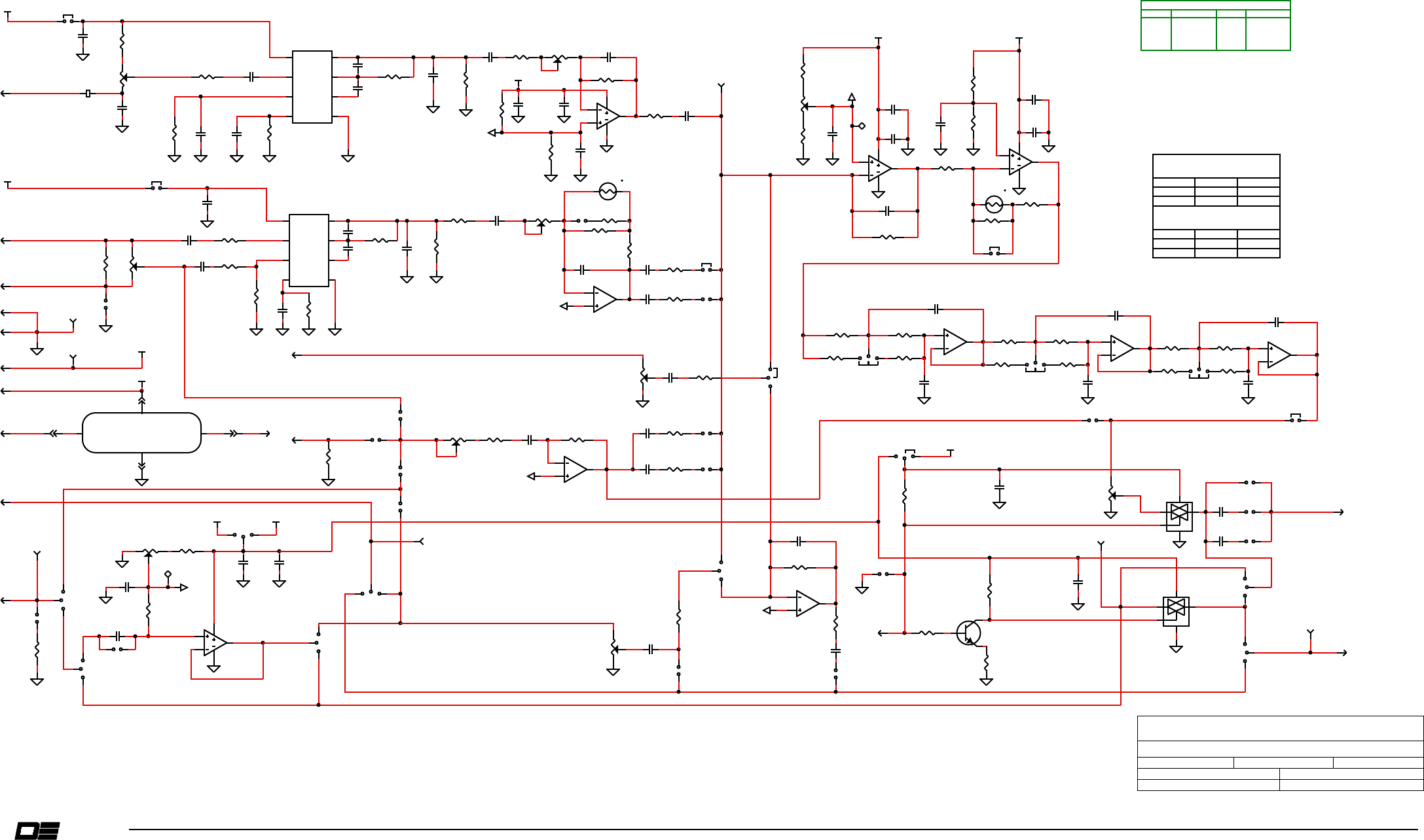
DANIELS
ELECTRONICS LTD.
TM
Low Frequency Modulation Configuration
Desig
Low Freq.
JU27X
JU27Y
JU31
JU35X
Not Installed
Not Installed
Not Installed
Not Installed
JU35Y
JU37
JU38X
JU38Y
Installed
Not Installed
Not Installed
Installed
Desig
Low Freq.
T
VICTORIA B.C.
DE
DANIELS
ELECTRONICS
T
5-9
Transmitter Main Board Instruction Manual
5
.
4
.
2
A
ud
i
o
Pr
o
ce
ss
o
r
S
c
h
e
m
a
t
i
c
D
i
a
g
ra
m
V
1
.
6
DWG REV DATE: 28 NOVEMBER 1997
DWG No: MT3APM2C
Not Installed if TOT circuitry installed
in Tx Main PCB 43-920917
NOTE: 400 MHz CTCSS Subtones from an Enhanced
Synthesizer are routed by installing jumpers JU35Y
(remove JU35X), JU36Y (remove JU36X) and JU37.
NOTE: For Low Frequency Modulation, short pins P4-1
and P4-3 together.
JU39
JU20-JU22
R76
U6-U7
R90
TP2J4
U10
P8
R53-R60
Q1
Q2
C58
C1,C2
FB1
----- ----- -----
UNUSED REFERENCE DESIGNATORS
HIGHEST REFERENCE DESIGNATORS
LOW FREQUENCY / DIRECT
MODULATION OUTPUT
XY
h
i
gh = vo
i
ce
l
o
w
= da
t
a
BOARD REV: VERSION 1.6
BOARD No: 43-911916
DEVIATION
CONTROL
Y
X
Y
X
Y
X
YX
YX
Y
X
Y
X
Y X
Y X
Y
X
Y
X
Y
X
+
+
+
+
+
+
+
DIRECT
MODULATION
INPUT
APRVD:
DWN BY: MICHAEL GAUBE
DATE: 19 SEPTEMBER 1991
TITLE: MT-3 TX AUDIO PROCESSOR SCHEMATIC DIAGRAM
+
MODULATION
OUTPUT
BALANCED INPUT
MICROPHONE INPUT
LEVEL CONTROL
6 POLE BUTTERWORTH FILTER
BALANCED
COMPRESSION
CONTROL
+
PRE-EMPHASIS
FLAT AUDIO
+
+
+
PRE-EMPHASIS
FLAT AUDIO
MICROPHONE
AGC PREAMP
MICROPHONE
COMPRESSION
CONTROL
SYMMETRY
ADJUST
BALANCED
AGC PREAMP
BALANCED
INPUT LEVEL
CONTROL
AUXILIARY INPUT
604R
R1
100nF
C4
10nF
C5
10nF
C6
6k81
R3
10nF
C7 47uF
C8 221k
R4
3
4
5
1 6
2
7
8
SL6270
U1
2.2uF
C10
100nF
C9
1k00
R6
150pF
C11
1k00
R5
20k0
R7
680nF
C12
221k
R9
10pF
C13
4.7nF
C16
100k
R16
150pF
C19
10nF
C17
49k9
R15
100nF
C28
4.7uF
C29
1k50
R32
47uF
C31 221k
R34
3
4
5
1 6
2
7
8
SL6270
U2
5k
R31
681R
R30 4.7uF
C30
1k50
R33 6.8µF
C33
4.7nF
C32
1k00
R36
150pF
C34
1k00
R35
330nF
C35
100k
R38
20k0
R37
10pF
C36 1k50
R40
4.7nF
C37
11k8
R41
50k
R29
221k
R50
27k4
R49 150nF
C41 1k50
R51
4.7nF
C43
22nF
C23
3k48
R26
3k48
R25
10nF
C24
15nF
C25
13k3
R28
13k3
R27
1.0nF
C26
FB1
100nF
C14
11k8
R52
2k21
R20
49k9
R13
330nF
C39
1.0uF
C40
11k8
R43
5k
R42
5k
R44
100nF
C20
49k9
R11
100k
R8
33nF
C27
330nF
C38
330nF
C44
100k
R48
4k53
R46
49k9
R21
49k9
R22
4k53
R17
681R
R18
68k1
R80
221k
R39
10k
R81
10nF
C21
5k11
R24
5k11
R23
10nF
C22
100nF
C18
300R
R19
R12
11k8
10nF
C15
27k4
R82
27k4
R83
22k1
R86
1.0uF
C47
JU3
JU4
JU5
JU12
JU2
JU9
JU10
JU14
JU15
JU7
JU8
JU32
JU33
+8.0V_SWD
+8.0V_SWD+8.0V_SWD
+8.0V_SWD
+9.5V_CONTINUOUS
39k2
R84
JU24 JU25 JU26
JU27
JU29
JU28
39k2
R85
100k
R8922k1
R87
49k9
R78
49k9
R79
Q2
BC817-25
100k
R88
4.7uF
C50 100nF
C51
27k4
R74
10nF
C49
JU1
+8.0V_SWD
JU31
JU11
JU13
20k0
R77
4.7uF
C3 4.7uF
C52 4.7uF
C54
10nF
C53
4.7uF
C55
3
28
4
1
MC33172
U3a
5
67
MC33172
U3b
5
67
U8b
MC33172
5
67
MC33172
U4b
4.7uF
C56
1.0uF
C48
221k
R73
63k4
R71
JU30
JU23
JU39
JU38
150pF
C58
JU16
JU36
2
38
4
1
MC33172
U8a
2
38
4
1
U4
MC33172
a
2
34
11
1
MC33174
U5a
5
67
U5
MC33174
b
10
98
c
MC33174
U5
12
13 14
U5
MC33174
d
JU35
JU34
39k2
R45
JU37
1.0uF
C57
39k2
R72
221k
R61
3
P1
2
P1
1
P1
4
P1
3
P3
3
P2
4
P2
1
P2
1
P4
3
P4
2
P2
1
P3
2
P4
4
P4
TP1
TP2
4k53
R47
1
2
3
50k
R14
5k
R2
50k
R75
1
J2 1
J4
1J3
1J1
1
P8
1
P7
1
P6
1P5
4
P3 2
P3
1 2
3
4
5
TC4S66F
U9
MT-3 TX TIME-OUT-TIMER
10k
R90
JU6
JU19
1 2
3
4
5
TC4S66F
U10
JU17
JU18
1
P9
1
P10
1
P11
1
P13
1
P12
+8.0V_SWD
+9.5V_CONTINUOUS
+8.0V_SWD
1P15
1P14
49k9
R10
+8.0V_SWD
MICROPHONE INPUT
TO_PIN_3_OF_U4
SUBTONE INPUT 1
TONE/DIGITAL I/P
V offset
V offset
Tx Audio Control
SUBTONE INPUT 2
TO_PIN_3_OF_U3
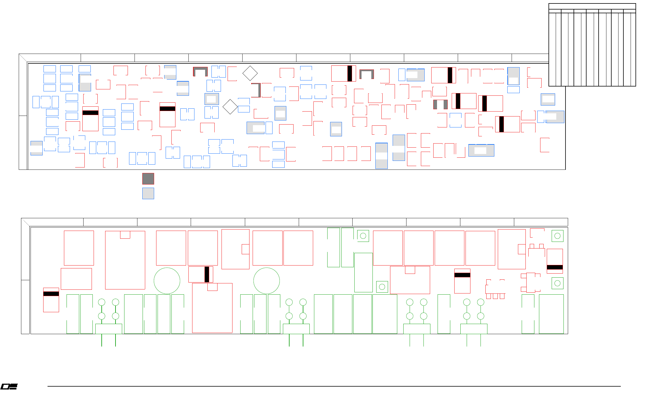
VICTORIA B.C .
DANIELS
ELECTRONICS
DRAWN BY: SHANE A
DWG REV DATE: 23 APR. 99
DATE: 19 APRIL 1996
DWG No: XXXXXAT1
TITLE: AM TRANSMITTER
D
TITLE: AM TRANSMITTER SURFACE MOUNT LAYOUT TITLE: FM TX AUDIO PROCESSOR BOARD OUTLINE
ELECTRONICS
PCB 43-911918
DWG No: TXADPROAS1
TITLE: MT-3 Tx Audio Processor SM Layout
- COMPONENTS NOT INSTALLED
DWG No: TXADPROAS2B
TITLE: MT-3 Tx Audio Processor SM Layout / Jumpers
- JUMPERS INSTALLED
FB1
DWG No: TXADPROAS3B
TITLE: MT-3 Tx Audio Processor SM Designations
R2
5k POT
MICROPHONE
INPUT LEVEL
CONTROL U1
SA5780
C8
10µF
R31
5k POT
BALANCE
INPUT LEVEL
CONTROL
R38
100k POT
BALANCE
COMPRESSION
CONTROL
U3
MC33172
R48
100k POT
AUXILIARY
INPUT LEVEL
CONTROL
R14
50k POT
SYMMETRY
ADJUST
U5
MC33174
R42
5k POT
SUBTONE
INPUT 1
CONTROL
LEVEL
U4
MC33172
R29
50k POT
DEVIATION
CONTROL
R75
50k POT
DC LEVEL
ADJUST
R36
50k POT
TCXO LEVEL
ADJUST
C45
4.7µF
C55
4.7µF
U8
MC33172 Q2
BC817
U9
TC4S66F
U10
TC4S66F
JU33 JU8
R77
20k0
R55
49k9 JU18
JU19
XY
JU31
JU28
X
Y
JU34
XY
JU35
X
Y
R79
49k9
C50
4.7µF
JU20
X
Y
JU30
Y
X
JU38
X
Y
R90
10k0
R72
0R0
R76
0R0
R9
49k9 C10
10nF
JU21 JU1
X
Y
X
YR74
27k4
R8
49k9
R43
11k8
JU39
R47
4k53
JU27
XY
JU4 JU29 R52
11k8
R41
49k9 R49
27k4
R50
221k
JU6
JU22
X Y
C52
4.7µF
JU7
JU16
R73
221k
C18
100nF
C49
10nF
JU14
JU10
JU9
JU15
R16
100k
R53
N/I
C17
10nF
R15
49k9
JU23
JU13 JU12
C3
4.7µF
JU2
JU11
JU17
JU3
X
Y
JU24
Y
X
JU25
JU26
X
Y
X
Y
C2
2.2µF
C7
2.2µF
C9
4.7µF
C30
4.7µF
C54
4.7µF
C5
10nF
C4
100nF
R1
604R
R7
37k4
R3
5k11
R37
49k9
R85
39k2
R20
SEL
R5
8k25
R32
470k
R33
1k50
C15
10nF R11
49k9
R4
3k01
R6
N/I
R18
SEL
R30
681R
R10
49k9
R54
274R
R35
68k1
C36
10pF
R39
221k
R71
63k4
R46
4k53
R13
49k9 R80
68k1
R34
75k0
C12
1nF
R21
49k9 C53
10nF
R17
SEL
R88
100k R27
13k3 R28
13k3 R89
100k
R86
22k1
R87
22k1
R25
3k48
R26
3k48
R24
5k11 R23
5k11
R84
39k2
JU44
XY
JU5
JU37
JU43
JU42
JU32
C51
100nF
R12
N/I
R51
1k50
R40
1k50
R44
0R0
X
Y
Y
X
C11
100nF
JU36
Y
X
JU40
R45
N/I
C20
100nF
R22
49k9
DWG No: TXADPROAT1
TITLE: MT-3 Tx Audio Processor Through Hole Layout
4
1
2
3
4
1
2
3
4
1
2
3
4
1
2
3
DWG No: TXADPROAT2
TITLE: MT-3 Tx Audio Processor Through Hole Designations
C24
10nF C47
1.0µF
C46
100nF
C27
33nF
C48
1.0µF
C44
330nF
C38
330nF
C41
150nF
C23
22nF
C25
15nF
C26
1.0nF
C21
10nF
C22
10nF
C35
330nF
C6
10nF
C1
220nF
R19
SEL R81
10k
C39
330nF
C37
4.7nF C43
4.7nF
P1 P2 P4 P3
1
2
A B C D E F G H I J
5-10
5.5 Audio Processor Electrical Assembly (Version 1.8)
5.5.1 Audio Processor Component Layout
Transmitter Main Board Instruction Manual
Solder Side
Component Side
TP2
TP1
MT3APM1B
3
4
K L M N O P Q R S T
R74 C2
R75 R3
R76 B1
R77 B2
R79 A2
R80 F2
R81 O4
R84 I2
R85 I2
R86 H2
R87 H2
R88 F2
R89 G2
R90 B1
TP1 D1
TP2 E1
U1 L3
U3 N3
U4 R3
U5 N4
U8 S3
U9 S4
U10 T4
JU7 C1
JU8 A2
JU9 D1
JU10D1
JU11H1
JU12F1
JU13F1
JU14 D1
JU15D1
JU16C1
JU17H2
JU18D2
JU19B2
JU20A1
JU21B2
JU22E2
JU23F1
JU24 I2
JU25 G2
JU26 G2
JU27 D2
JU28 A2
JU29 D2
JU30 A1
JU31 A2
R9 B1
R10 H1
R11 G1
R12 D1
R13 F2
R14 O3
R15 E1
R16 D2
R17 G2
R18 H2
R19 K3
R20 I2
R21 G1
R22 G1
R23 H2
R24 H2
R25 H2
R26 H2
R27 F2
R28 F2
R29 R3
R30 H1
R31 M3
R32 I1
R33 I1
R34 G1
R35 G1
R36 S3
R37 I2
R38 N3
R39 F1
R40 E1
R41 E2
R42 Q3
R43 C2
R44 E1
R45 G1
R46 F1
R47 C2
R48 O3
R49 E2
R50 E2
R51 D1
R52 E2
R53 E1
R54 G1
R55 A2
R71 F1
R72 B1
R73 C1
C36 G1
C37 P3
C38 P4
C39 Q3
C41 P4
C43 P3
C44 Q4
C45 S4
C46 T4
C47 T4
C48 Q4
C49 C1
C50 B2
C51 T3
C52 C2
C53 G1
C54 N3
C55 T3
FB1 K3
JU1 B2
JU2 F2
JU3 J1
JU4 D2
JU5 E2
JU6 E1
C1 K4
C2 I1
C3 F1
C4 J1
C5 J2
C6 L4
C7 I1
C8 K4
C9 I2
C10 B1
C11 I1
C12 G2
C15 G1
C17 E1
C18 C1
C20 H1
C21 M4
C22 M4
C23 O4
C24 M4
C25 O4
C26 O4
C27 R4
C30 H1
C35 L4
COMPONENT LOCATION TABLE
DES LOC
DES LOC DES LOC DES LOC DES LOC DES LOC DES LOC
JU32 A2
JU33 A2
JU34 A1
JU35 A1
JU36 J1
JU37 E1
JU38 B1
JU39 C2
JU40 J1
JU42 E1
JU43 C1
JU44 C2
P1 L4
P2 O4
P3 S4
P4 R4
Q2 T3
R1 J1
R2 K3
R3 J2
R4 H1
R5 I1
R6 H1
R7 J1
R8 C1
ELECTRONICS LTD.
DANIELS TM
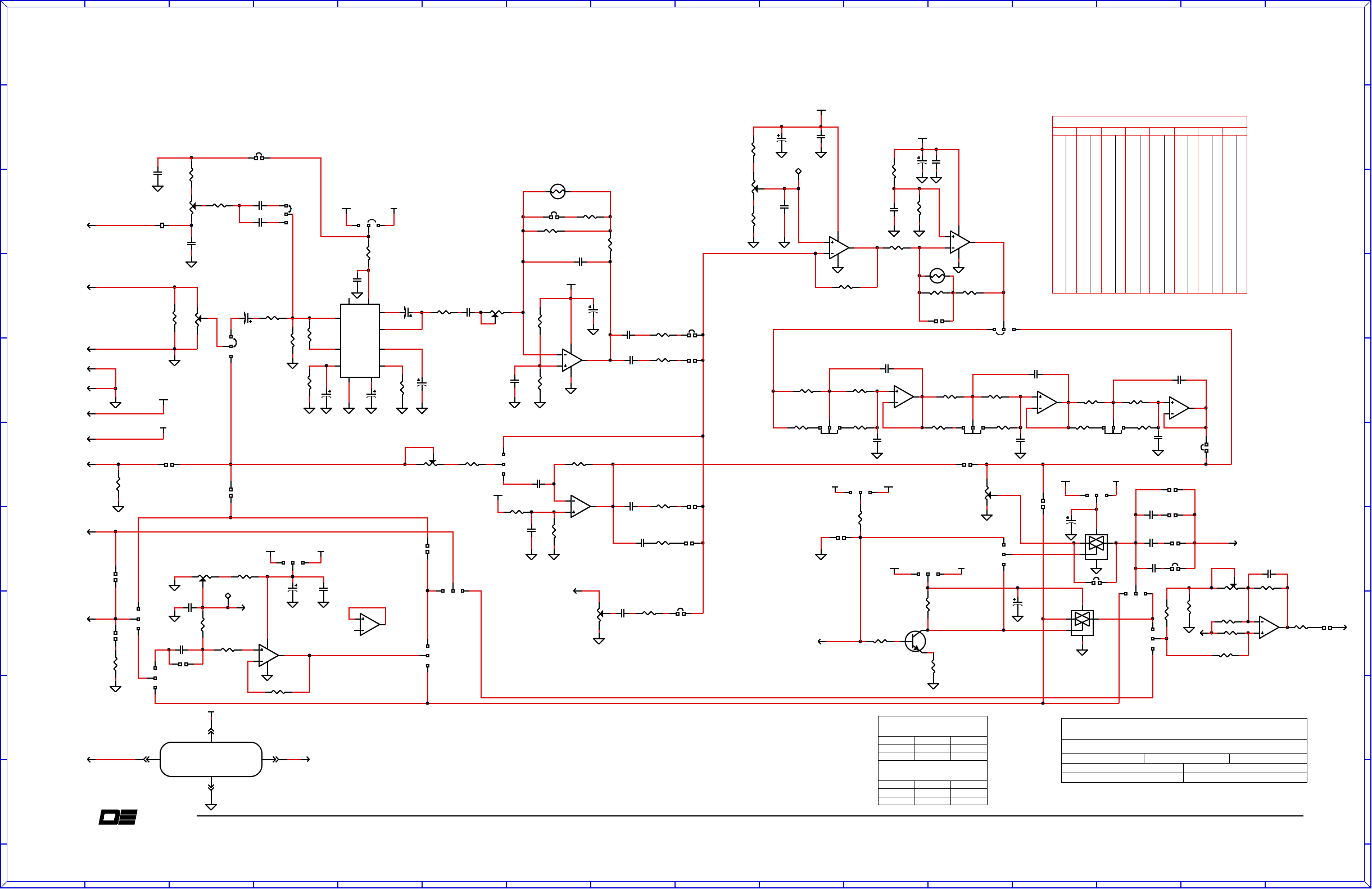
A
A
B
B
C
C
D
D
E
E
F
F
G
G
H
H
I
I
J
J
K
K
L
L
M
M
N
N
O
O
P
P
1 1
2 2
3 3
4 4
5 5
6 6
7 7
8 8
9 9
1 1
0 0
DANIELS
ELECTRONICS LTD.
TM
JU32 N7
JU33 N7
JU34 N7
JU35 N8
JU36 E3
JU37 P8
JU38 F7
JU39 B8
JU40 C2
JU42 M6
JU43 M7
JU44 L7
P1-1 A4
P1-2 A4
P1-3 A3
P1-4 A5
P2-1 A6
P2-2 G7
P2-3 A5
P2-4 A5
P3-1 O7
P3-2 D9
P3-3 A5
P3-4 A9
P4-1 A7
R47 B8
R48 E6
R49 F6
R50 G6
R51 H6
R52 H7
R53 O8
R54 P8
R55 K8
R71 G3
R72 C8
R73 C8
R74 C7
R75 C7
R76 D8
R77 K6
R79 K7
R80 G3
R81 G2
R84 J5
R85 J5
R86 K5
R87 L5
R88 M5
R89 N5
JU7 L6
JU8 N6
JU9 H4
JU10H5
JU11C4
JU12B6
JU13C6
JU14H6
JU15H7
JU16H8
JU17K4
JU18J7
JU19J6
JU20K7
JU21M6
JU22L4
JU23E7
JU24 J5
JU25 L5
JU26 M5
JU27 B8
JU28 B8
JU29 B8
JU30 E8
JU31 N6
P4-2 P8
P4-3 A8
P4-4 J8
Q2 K8
R1 C2
R2 C3
R3 C3
R4 E3
R5 D4
R6 D5
R7 E5
R8 F6
R9 G7
R10 G4
R11 G5
R12 N7
R13 I2
R14 I2
R15 I3
R16 J4
R17 K3
R18 K4
R19 K3
R20 L4
R21 K2
R22 K3
R23 J5
R24 J5
R25 L5
R26 L5
R27 M5
R28 N5
R29 L6
R30 B4
R31 C4
R32 D4
R33 C4
R34 O7
R35 N7
R36 O7
R37 F4
R38 F4
R39 H3
R40 H4
R41 H5
R42 G8
R43 H8
R44 O8
R45 O8
R46 B6
R90 K8
TOT B9
TP1 J2
TP2 C7
U1 D4
U3a G4
U3b O8
U4a J3
U4b G6
U5a L3
U5b K5
U5c M5
U5d N5
U8a C8
U8b E8
U9 M7
U10 M8
Vset C7
Vset O8
C36 G3
C37 H4
C38 H5
C39 H8
C41 G6
C43 H6
C44 H7
C45 M6
C46 N6
C47 N7
C48 B8
C49 C7
C50 D7
C51 D7
C52 J2
C53 K3
C54 K2
C55 L7
FB1 B3
JU1 D7
JU2 G3
JU3 D3
JU4 B7
JU5 F6
JU6 O6
C1 C3
C2 D5
C3 G4
C4 B2
C5 C3
C6 C3
C7 E5
C8 E5
C9 E4
C10 G7
C11 E4
C12 O7
C15 F5
C17 J3
C18 J2
C20 K2
C21 K5
C22 K5
C23 M5
C24 L5
C25 N5
C26 N5
C27 N7
C30 C4
C35 F4
COMPONENT LOCATION TABLE
DES LOC DES LOC DES LOC DES LOC DES LOC DES LOC DES LOC DES LOC
VICTORIA B.C.
DE
DANIELS
ELECTRONICS
5-11
Transmitter Main Board Instruction Manual
5
.
5
.
2
A
ud
i
o
Pr
o
ce
ss
o
r
S
c
h
e
m
a
t
i
c
D
i
a
g
ra
m
V
1
.
8
S
UBT
O
N
E
IN
P
UT
1
C
O
NTR
O
L L
EVE
L
DWG REV DATE: 19 NOVEMBER 98
BOARD No: 43-911918
DWG No: MT3APM2D
TITLE: MT-3 TX AUDIO PROCESSOR SCHEMATIC DIAGRAM
DATE: 12 MAY 98
YX
Y
X
Y
X
JU41 -----U2,U6,U7
R78,R82,R83
R56-R70C40,C42
C31-C34C19,C28,C29
C13,C14,C16
U10TP2
R90P4Q2
JU44FB1C55
BOARD REV: VERSION 1.8
AUXILIARY IN
P
UT
L
EVE
L C
O
NTR
O
L
OPTIONAL
DC L
EVE
L ADJU
S
T
PRE-EMPHASIS
FLAT
6 POLE BUTTERWORTH FILTER
NOT INSTALLED FOR DIGITAL MOD.
+9.5V CONTINUOUS
Y
X
Y
X
HIGHEST REFERENCE DESIGNATORS
UNUSED REFERENCE DESIGNATORS
-----
Y
Y
X
X
C
O
M
P
R
ESS
I
O
N
C
O
NTR
O
L
AGC PREAMP
Y
X
TCXO LEVEL ADJUST
DWN BY: STAN POLYAKOV
Y
X
LOW FREQUENCY / DIRECT
MODULATION OUTPUT
h
i
gh = vo
i
ce
l
o
w
= da
t
a
D
EV
IATI
O
N
C
O
NTR
O
L
Y
X
Y
X
Y
X
Y
XY
X
Y
X
Y
X
Y
X
Y
X
Y
X
DIRECT
MODULATION
INPUT
APRVD:
M
O
DULATI
O
N
O
UT
P
UT
BALANCED INPUT
MICR
O
P
H
O
N
E
IN
P
UT
L
EVE
L C
O
NTR
O
L
PRE-EMPHASIS
FLAT AUDIO
PRE-EMPHASIS
FLAT AUDIO
S
YMM
E
TRY
ADJU
S
T
BALANC
E
D
IN
P
UT L
EVE
L
C
O
NTR
O
L
3
P1
2
P1
1
P1
4
P1
3
P3
3
P2
1
P2
1
P4
3
P4
2
P2
1
P3
2
P4
4
P4
+9.5V CONTINUOUS
1 2
100nF
C46
1
2
JU4
1 2
JU37
1 2
R76
0R0
1 2
R72
0R0
1 2
R8
49K9
1 2
JU16
4
P2
+9.5V CONTINUOUS
12
C30
4.7uF
1
2C7
2.2uF
12
C9
4.7uF 1
2
C3
4.7uF
1
2
R10
49K9
1
2
R11
49K9
1
2C2
2.2uF
1
2C8
10uF
213
JU22
1
2
10nF
C10
1
2
10nF
C15
+9.5V CONTINUOUS +9.5V CONTINUOUS
+9.5V CONTINUOUS
1
2
C45
4.7uF
1
2
C55
4.7uF
1 2
JU18
1 2
C43
4.7nF
1 2
C44
330nF
1 2
R51
1K50
1 2
R52
11K8
1 2
JU14
1 2
JU15
1 2
R50
221K0
1 2
R49
27K4
1
2
R9
49K9
123
R48
100K0
1 2
JU12
1
2
JU13
1
2
3
R42
5K0
1
2
JU23
1
2
R46
4K53
123
JU38
1
2
3
JU30
1
2
3
JU1
1
2
C51
100nF
1
2
C50
4.7uF
1 2
R74
27K4
1
2
3
R75
50K0
1 2
C49
10nF
1 2
C48
1.0uF
1 2
JU29
1
2
JU39
1
2
R47
4K53 1
2
3
JU28
1
2
3
JU27
8
3
21
4
aU8
MC33172
6
57
bU8
MC33172
1
2
3
R38
100K0
1 2
R71
63K4
1 2
R80
68K1
1
2
R39
221K0
1 2
C36
10pF
1 2
C39
330nF
1 2
R43
11K8
1 2
C38
330nF
1 2
R40
1K50
1 2
C37
4.7nF
1 2
JU9
1 2
JU10
1
2
49K9
R13
1
2
49K9
R15
1 2
100K0
R16
1
2
10nF
C17
8
3
21
4
MC33172
aU4
6
57
MC33172
U3b
1
2
49K9
R21
1
2
49K9
R22
1
2
10nF
C53
1 2
4K53
R17
1 2
2K21
R20
1 2
5K11
R23
1 2
5K11
R24
1 2
39K2
R84
1 2
39K2
R85
1 2
3K48
R25
1 2
3K48
R26
1 2
22K1
R86
1 2
22K1
R87
1
210nF
C22 1
210nF
C24
1 2
10nF
C21
1 2
22nF
C23
6
57
MC33174
bU5
9
10 8
MC33174
cU5
13
12 14
MC33174
dU5
1 2
13K3
R27
1 2
13K3
R28
1 2
100K0
R88
1 2
100K0
R89
1 2
15nF
C25
1
21.0nF
C26
1 2
1.0uF
C47
1 2
33nF
C27
1 2
JU8
1 2
JU7
1
2
3
50K0
R29
1 2
3
4
5
TC4S66F
U9
1 2
3
4
5
TC4S66F
U10
1
2
49K9
R79
1 2
49K9
R55
1
210K0
R90
E
B
C
BC817-25
Q2
1
2
3
JU35
123
JU34
1
2
100nF
C4
1
210nF
C5
1
2
604R0
R1
1
2
3
5K0
R2
1
2
681R0
R30 1 2
1K50
R33
1 2
FB1
1 2
330nF
C35
1 2
150nF
C41
1
2
3
50K0
R14
1
2221K0
R73
1
220K0
R77
TP2
TP1
4
3
21
8U3a
MC33172
6
57
U4b
MC33172
2
34
1
11
U5a
MC33174
1 2
R81
10K
1
2
3
JU24
1
2
3
JU25
1
2
3
JU26
Vcc
Rect in
Rect Cap
Output
Input 1
GND
G in
Mute
Filt
VRef
I Ref
13
11
10
8
12
14
16
7 15
5
6
U1
SA578D
+8.0V SWD
+8.0V SWD
+8.0V SWD
+8.0V SWD
+8.0V SWD
+8.0V SWD
+8.0V SWD
+8.0V SWD
+8.0V SWD
+8.0V SWD
1
2JU6
1
2
JU42
+9.5V CONTINUOUS
MT-3 TX TIME-OUT-TIMER
J3
J2 J4
J1
P7
P6
P5
P84
P3 2
P3
1
1
1
2
3
5K0
R31
1
2
N/I
R12
1 2
0R0
R44
1 2
N/I
R53
1
2
N/I
R6
2
1
3
JU11
1 2
N/I
R45
1
2
R7
37K4
1
2
R5
8K25
1
2
R4
3K01
2
1 3
JU36
1
2
3JU3 1 2
JU2
1
2
470K0
R32
1 2
R37
49K9
1 2
R41
49K9
1 2
1K2
R19
1 2
1K0
R18
1
2
4.7uF
C54 1
2100nF
C20
1
2
4.7uF
C52 1
2
100nF
C18
1
2
100nF
C11
1 2
75K0
R34
1 2
1.0nF
C12
1 2
274R0
R54
1
268K1
R35
123
50K0
R36
1 2
10nF
C6
1 2
220nF
C1
1 2
5K11
R3
1 2
JU40
1
2
3
JU5
1 2
JU17
1
2
3JU20
1
2
3
JU19
1
2
3
JU44
1
2
3JU21
1 2
JU32
1 2
JU43
1 2
JU33
1 2
JU31
MICROPHONE INPUT
SUBTONE INPUT 1
TONE/DIGITAL I/P
SUBTONE INPUT 2
Tx Audio Control
Vset
Vset

DE
DANIELS
ELECTRONICS
5-12
Transmitter Main Board Instruction Manual
This Page Intentionally Left Blank

Transmitter Main Board Instruction Manual
6-1
6
PARTS LISTS
invisible
text
6.1 Transmitter Main Board Parts List
invisible
text
6.1.1
Transmitter Main Board Electrical Parts List
Ref
Desig Description Part No.
C1
CAP.,
SM,
10µF
TANT., 10%, 35V 1055-6D106K35
C2
CAP.,
SM,
1.0µF
TANT., 20%, 35V 1055-5B105M35
C3
CAP.,
SM,
10µF
TANT., 20%, 16V 1055-6C106M16
C4
CAP.,
SM,
1.0µF
TANT., 20%, 16V 1055-5A105M16
C5
CAP.,
SM,
100nF
CER,
0805, X7R 1008-5A104K5R
C6,
C7
CAP.,
SM,
10nF
CER,
0805,
X7R,
50V 1008-4A103K5R
C8
CAP.,
SM,
100nF
CER,
0805, X7R 1008-5A104K5R
C10
CAP.,
SM,
10µF
CER/2225
50 X7R 1008-6H105J5R
C12- C14
CAP.,
SM,
10nF
CER,
0805,
X7R,
50V 1008-4A103K5R
C15
CAP.,
SM,
4.7µF
TANT., 10%, 16V
1055-5B475K16
C20
CAP.,
SM,
4.7µF
TANT., 10%, 16V
1055-5B475K16
C21,
C22
CAP.,
SM,
100nF
CER,0805,X7R,5
0V 1008-5A104K5R
C23
CAP.,
100nF
FILM,
MMK5, 10%, 63V 1016-5A104K63
D1 - D6 DIODE, BYD17J
RECTIFIER,
SOD-87
2101-BYD17J00
D7, D8 DIODE, BAS16, SWITCHING, DO35 2100-BAS16000
F1
FUSE,
3AMP FAST-BLO, 1-1/4 IN. 5604-5GAGC030 (Optional)
FH1,FH2
FUSE
CLIP,
O.250"DIAM.,
W/EAR 5609-C250P01B (Optional)
FSW1-4 SWITCH, BCD-10
STEPS,5
PIN,PCB 5273-10BCD001
JS1-1 SOCKET
STRIP,
1 ROW X 12 PIN 5016-SL112G08
JS1-13 SOCKET
STRIP,
1 ROW X 9 PIN 5016-SL109G08
JS2-1 SOCKET
STRIP,
1 ROW X 6 PIN 5016-SL106G08
JS3-1 SOCKET
STRIP,
1 ROW X 2 PIN 5016-SL102G08
LPF1-5
FILTER,
SM.
EMI/LPF,
360
PF,
FER.
1306-T361F2D5
LPF8
FILTER,
SM.
EMI/LPF,
360
PF,
FER.
1306-T361F2D5
LPF10
FILTER,
SM.
EMI/LPF,
360
PF,
FER.
1306-T361F2D5
LPF12
FILTER,
SM.
EMI/LPF,
360
PF,
FER.
1306-T361F2D5
LPF14-35
FILTER,
SM.
EMI/LPF,
360
PF,
FER.
1306-T361F2D5
PCB MT-3 TRANSMITTER, MAIN, VER 1.7 4321-10920917
Q1
TRANSISTOR,
BC817-25 NPN,
G.P.,
SOT-23 2120-BC817025
Q3-Q4
TRANSISTOR,
BC817-25 NPN,
G.P.,
SOT-23 2120-BC817025
Q5
MOSFET,
D5P06V P-CHANNEL, DPAK 2144-D5P06V00
Q6
TRANSISTOR,
BC817-25 NPN,
G.P.,
SOT-23 2120-BC817025
Q7
MOSFET,
D5P06V P-CHANNEL, DPAK 2144-D5P06V00
Q8
TRANSISTOR,
BC807-25
PNP,
G.P.,
SOT-23 2120-BC807025
Q9
MOSFET,
D15N06V N-CHANNEL, DPAK 2144-D15N06V0
Q10
TRANSISTOR,
PZT2222A NPN,
G.P.,
SOT-223 2120-PZT2222A
Q11
TRANSISTOR,
BC807-25
PNP,SOT23
2120-BC807025

6-2
Transmitter Main Board Instruction Manual
Ref
Desig Description Part No.
R1
RES.,
SM,
10R0 0805, 1%, 100 ppm 1150-1A10R0FP
R2
RES.,
SM,
27k4 0805, 1%, 100 ppm 1150-4A2742FP
R3
RES.,
SM,
1k00 0805, 1%, 100 ppm 1150-3A1001FP
R4
RES.,
SM,
27k4 0805, 1%, 100 ppm 1150-4A2742FP
R5
RES.,
SM,
10R0 0805, 1%, 100 ppm 1150-1A10R0FP
R6
RES.,
SM,
27k4 0805, 1%, 100 ppm 1150-4A2742FP
R7
RES.,
SM,
1k00 0805, 1%, 100 ppm 1150-3A1001FP
R8
RES.,
SM,
27k4 0805, 1%, 100 ppm 1150-4A2742FP
R9
RES.,
SM,
221k 0805, 1%, 100 ppm 1150-5A2213FP
R10
RES.,
SM,
100k 0805, 1%, 100 ppm 1150-5A1003FP
R11-R13
RES.,
SM,
27k4 0805, 1%, 100 ppm 1150-4A2742FP
R14-R16
RES.,
SM,
10K0 0805, 1%,100ppm 1150-4A1002FP
R17
RES.,
SM,
1k00 0805, 1%, 100 ppm 1150-3A1001FP
R18,R19
RES.,
SM,
10K0 0805, 1%,100ppm 1150-4A1002FP
R20
RES.,
SM,
68k1 0805, 1%, 100 ppm 1150-4A6812FP
R21
RES.,
SM,
10K0 0805, 1%,100ppm 1150-4A1002FP
R22
RES.,
SM,
68k1 0805, 1%, 100 ppm 1150-4A6812FP
R23
RES.,
SM,
10K0 0805, 1%,100ppm 1150-4A1002FP
R24
RES.,
SM,
68k1 0805, 1%, 100 ppm 1150-4A6812FP
R25
RES.,
SM,
27k4 0805, 1%, 100 ppm 1150-4A2742FP
R26
RES.,
SM,
1k00 0805, 1%, 100 ppm 1150-3A1001FP
R28
RES.,
SM,
15K0 0805, 1%, 100ppm 1150-4A1502FP
R29
RES.,
SM,
82k5 0805, 1%, 100 ppm 1150-4A8252FP
R30
RES.,
SM,
15K0 0805, 1%, 100ppm 1150-4A1502FP
R31
RES.,
SM,
221k 0805, 1%, 100ppm 1150-5A2213FP
R32
RES.,
SM,
1k00 0805, 1%, 100ppm 1150-3A1001FP
R33
RES.,
SM,
68k1 0805, 1%, 100ppm 1150-4A6812FP
R34,
R35
RES.,
SM,
27k4 0805, 1%, 100ppm 1150-4A2742FP
R36
RES.,
SM,
221k 0805, 1%, 100ppm 1150-5A2213FP
R37
RES.,
SM,
1k00 0805, 1%, 100ppm 1150-3A1001FP
R38
RES.,
SM,
100k 0805, 1%, 100ppm 1150-5A1003FP
R39
RES.,
SM,
221k 0805, 1%, 100ppm 1150-5A2213FP
R40
RES.,
SM,
10k0 0805, 1%, 100ppm 1150-4A1002FP
R41
RES.,
SM,
15k0 0805, 1%, 100ppm 1150-4A1502FP
R42
RES.,
OPT METAL
FILM,
5%,0.5W OPTIONAL
R43 - R46
RES.,
SM,
221k 0805, 1%, 100ppm 1150-5A2213FP
R47
RES.,
SM,
1k00 0805, 1%, 100ppm 1150-3A1001FP
RELAY1 RELAY, 9 Vdc, 2
FORM
C,
PCB MNT 5310-2C09P005 (Optional)
T1
TRANSFORMER,
SPT-196 1:1 AUDIO XFMR 1280-600P6005
U1 IC, MC33172 DUAL
OP-AMP,
S0-8 2302-33172N08
U2 IC, 4081 QUAD 2 INPUT AND, S0-14 2375-40810N14
U3, U4 IC, MMAD1108 8 DIODE ARRAY, S0-16 2331-11080N16
U6 IC,
LP2951,
PROG,
VOLT REG, SO-8 2305-29510N08
U7 IC, MC33172 DUAL OP
AMP,
SO-8 2302-33172N08
U8 IC, MC14536B
PROGRAM
TIMER, SO-16W 2375-45360W16

Transmitter Main Board Instruction Manual
6-3
6.1.2
Transmitter Main Board Mechanical Parts List
Description Part No. Qty.
CABLE, SMB-SMB PLUG, RG316,12cm $7910-WP0WP012 1
(Enhanced
Synth
and
Crystal Control)
CABLE, SMA-SMB PLUG, RG316,15cm $7910-SP0WP015 1 (Low Power Synth)
CABLE,SMA PL-SMB
PL,RG316,11cm
$7910-SP0WP011 1
(Reference
Input Opt.
Enhanced
Synth)
CABLE, SMA PLUG-PLUG,
RG316,
19 cm
$7910-SP0SP019
1
(Reference
Input Opt.
Low Power Synth)
CONN, TYPE F 48 MALE,
RA,
PCB MTG 3720-6048M0RA 1
CONN/RF,
SMA JACK-JACK
BULKHEAD
5118-J875BJ05 1
(Reference
Input Opt.
Low Power Synth)
PANEL,
REAR,
POS.4,
14HP
EXTRSN.
3702-63002101 1
FASTENER,
QUICK RELEASE 3702-10000120 4
GASKET,
BeCu,3FINGER,.25",CLIP
5630-12023250 2
HANDLE, FRONT PANEL,
14HP,
GREY 3702-10000614 1
HOLE PLUG, 0.25" HOLE, NYLON, BLACK
5671-250N062B
1
LOCKWASHER,
M3,
SPLIT,A2
STEEL 5814-3M0LK00S 4
MIC CONN, 4 PIN MALE, BLACK 5040-114ST0BK 1
NAMEPLATE, BLANK,
14HP,
ALUM. 3702-10001214 1
NUT,
M2.5,
HEX,
5.0mm,
STEEL/Ni 5813-2M5HX50N 2
NUT,
M2.5,
SQUARE,
5.0mm,
ZINC 5813-2M5SQ50Z 2
NUT
PRESS,
M2.5,
5.6mm
OD,
PC
MNT 5833-T2M55615 1
PANEL/FRNT,W/IDENT:TX-EXTR.VER 3802-61002101 1
PANEL,
REAR,POS.4,14HP
EXTRSN. 3702-63002101 1
SCREW,
M3 x 8, PAN/PHIL, BLACK 5812-3M0PP08T 4
SCREW,
M3 x8,OVAL
C/S/PHIL,A2
5812-3M0VP08S 4
SCREW,
M2.5
X 10,
CHEESE/SLOT,
A2 5812-2M5CS10S 2
SCREW,
M2.5
X 12, FLAT/PHIL, Ni 5812-2M5FP12N 2
SCREW,
M3 X 6, OVAL
C/S/PHIL,
Ni 5812-3M0VP06N 2
SCREW,
M3 X 6 PAN/PHIL, A2
5812-3M0PP06S
4
SCREW,
M5 X 8 FLAT/PHIL, A2
5812-5M0FP08S
4
TAB, GROUND, MT-3
SYNTH.,
BRASS 3702-67800905 2 (Low Power Synth)
WIRE, PVC-STRANDED, 22 AWG BLK., 10.5cm 7110-22S07300 1
WIRE, PVC-STRANDED, 22 AWG BRN., 10cm 7110-22S07301 1
WIRE, PVC-STRANDED, 22 AWG
ORG.,
9.5cm 7110-22S07303 1
WIRE, PVC-STRANDED, 22 AWG RED, 13.5cm 7110-22S07302 1
WIRE, PVC-STRANDED, 22 AWG
YEL.,
9.5cm 7110-22S07304 1
WIRE, PVC-STRANDED, 22 AWG BLUE, 10cm 7110-22S07306 1

6-4
Transmitter Main Board Instruction Manual
6.1.3 MT-3 Front Panel Board Electrical Parts List
Ref
Desig Description Part No.
D1 LED, RED, 5 mm OD, T-1 3/4 2010-503001RD
PF1 HEADER,
0.1",
RA,
2 ROW X 2 PIN 5010-H202RA9T
PF2 HEADER,
0.1",
RA,
2 ROW X 2 PIN 5010-H202RA9T
SW1 SWITCH, TOG/DPDT, ON-OFF-ON, PCB/STR 5215-T2031V02
PCB MT-3 TX FRONT PANEL 4321-40921211
6.2 MT-3 Audio Processor Parts List (Version 1.6)
invisible
text
6.2.1 MT-3 Audio Processor Electrical Parts List (Version 1.6)
Ref
Desig Description Part No.
C3
CAP.,
SM,
4.7µF
TANT., 10%, 16V 1055-5B475K16
C4
CAP.,
SM,
100nF
CER,0805,X7R,50V
1008-5A104K5R
C5 - C7
CAP.,
SM,
10nF
CER,0805,X7R,50V
1008-4A103K5R
C8
CAP.,
SM,
47uF TANT., 20%, 16V 1055-6D476M16
C9
CAP.,
100nF
FILM,
MMK5, 10%, 63V 1016-5A104K63
C10
CAP.,
SM,
2.2µF
TANT., 10%, 20V 1055-5B225K20
C11
CAP.,
SM,
150pF
CER,
0805, C0G
1008-2AI5IJIG
C12
CAP.,
680nF
FILM,
MMK5, 10%, 50V 1016-5D684K50
C13
CAP.,
SM,
10pF
CER,
0805, C0G 1008-1A100J1G
C14
CAP.,
SM,
100nF
CER,0805,X7R,50V
1008-5A104K5R
C15
CAP.,
SM,
10nF
CER,0805,X7R,50V
1008-4A103K5R
C16
CAP.,
4.7nF
FILM,
MMK5, 10%, 63V 1016-3A472K63
C17
CAP.,
SM,
10nF
CER,0805,X7R,50V
1008-4A103K5R
C18
CAP.,
SM,
100nF
CER,0805,X7R,50V
1008-5A104K5R
C19
CAP.,
SM,
150pF
CER,
0805, C0G
1008-2AI5IJIG
C20
CAP.,
SM,
100nF
CER,0805,X7R,50V
1008-5A104K5R
C21,
C22
CAP.,
10nF
FILM,
MMK5, 10%, 63V 1016-4A103K63
C23
CAP.,
22nF
FILM,
MMK5, 10%, 63V 1016-4A223K63
C24
CAP.,
10nF
FILM,
MMK5, 10%, 63V 1016-4A103K63
C25
CAP.,
15nF
FILM,
MMK5, 10%, 63V 1016-4A153K63
C26
CAP.,
1.0nF
FILM,
MMK5, 10%, 63V 1016-3A102K63
C27
CAP.,
33nF
FILM,
MMK5, 10%, 63V 1016-4A333K63
C28
CAP.,
SM,
100nF
CER,0805,X7R,50V
1008-5A104K5R
C29,
C30
CAP.,
SM,
4.7µF
TANT., 10%, 16V
1055-5B475K16
C31
CAP.,
SM,
47uF TANT., 20%, 16V 1055-6D476M16
C32
CAP.,
4.7nF
FILM,
MMK5, 10%, 63V 1016-3A472K63
C33
CAP.,
SM,
6.8µF
TANT., 20%, 10V 1055-5B685M10
C34
CAP.,
SM,
150pF
CER,
0805, C0G
1008-2AI5IJIG
C35
CAP.,
330nF
FILM,
MMK5, 10%, 50V
1016-5B334K50
C36
CAP.,
SM,
10pF
CER,
0805, C0G 1008-1A100J1G
C37
CAP.,
4.7nF
FILM,
MMK5, 10%, 63V 1016-3A472K63
C38,
C39
CAP.,
330nF
FILM,
MMK5, 10%, 50V
1016-5B334K50

Transmitter Main Board Instruction Manual
6-5
Ref
Desig Description Part No.
C40
CAP.,
1.0µF
FILM,
MMK5, 10%, 50V 1016-6D105K50
C41
CAP.,
150nF
FILM,
MMK5, 10%, 63V
1016-5B154K63
C42
CAP.,
N/I NOT INSTALLED
C43
CAP.,
4.7nF
FIL
M,
MMK5, 10%, 63V 1016-3A472K63
C44
CAP.,
330nF
FILM,
MMK5, 10%, 50V
1016-5B334K50
C47,
C48
CAP.,
1.0µF
FILM,
MMK5, 10%, 50V 1016-6D105K50
C49
CAP.,
SM,
10nF
CER,0805,X7R,50V
1008-4A103K5R
C50
CAP.,
SM,
4.7µF
TANT., 10%, 16V
1055-5B475K16
C51
CAP.,
SM, 100nF
CER,0805,X7R,50V
1008-5A104K5R
C52
CAP.,
SM,
4.7µF
TANT., 10%, 16V
1055-5B475K16
C53
CAP.,
SM,
10nF
CER,0805,X7R,50V
1008-4A103K5R
C54 - C56
CAP.,
SM,
4.7µF
TANT., 10%, 16V
1055-5B475K16
C57
CAP.,
1.0µF
FILM,
MMK5, 10%, 50V 1016-6D105K50
C58 C
AP.,
SM,
150pF
CER,
0805, C0G
1008-2AI5IJIG
FB1 FERRITE BEAD, 43 MIX 1812 PKG 1213-43181200
P1 - P4 HEADER,
0.1",
R/A,
2 ROW X 2PIN 5010-H202RA9T
PCB AUDIO
PROCESSOR,
MT-3 TX 4321-30911916
Q2
TRANSISTOR,
BC817-25 NPN, SOT-23 2120-BC817025
R1
RES.
,
SM,
604R 0805, 1%, 100ppm 1150-2A6040FP
R2
POT.,
SM/4mm
SQ,
5k 11T, SIDE ADJUST 1174-DM2502J0
R3
RES.,
SM,
6k81 0805, 1%, 100ppm 1150-3A6811FP
R4
RES.,
SM,
221k 0805, 1%, 100ppm 1150-4A2212FP
R5,
R6
RES.,
SM,
1k00 0805, 1%, 100ppm 1150-3A1001FP
R7 R
ES.,
SM,
20k0 0805, 1%, 100ppm 1150-4A2002FP
R8
POT.,
SM/4mm
SQ,
100k 11T, SIDE ADJUST 1174-DM4104J0
R9
RES.,
SM,
221k 0805, 1%, 100ppm 1150-4A2212FP
R10,
R11
RES.,
SM,
49k9 0805, 1%, 100ppm 1150-4A4992FP
R12
RES.,
SM,
11k8 0805, 1%, 100ppm 1150-4A1182FP
R13
RES.,
SM,
49k9 0805, 1%, 100ppm 1150-4A4992FP
R14
POT.,
SM/4mm
SQ,
50k 11T, SIDE ADJUST 1174-DM3503JO
R15
RES.,
SM,
49k9 0805, 1%, 100ppm 1150-4A4992FP
R16
RES.,
SM,
100k 0805, 1%, 100ppm 1150-5A1003FP
R17
RES.,
SM,
4k53 0805, 1%, 100ppm 1150-3A45315P
R18
RES.,
SM,
681R 0805, 1%, 100ppm 1150-2A6810FP
R19
THERMISTOR,
10k NTC, 10%, RADL. 1180-4RDG103K
R20
RES.,
SM,
2k21 0805, 1%, 100ppm 1150-3A2211FP
R21,
R22
RES.,
SM,
49k9 0805, 1%, 100ppm 1150-4A4992FP
R23,
R24
RES.,
SM,
5k11 0805, 1%, 100ppm 1150-3A5111FP
R25,
R26
RES.,
SM,
3k48 0805, 1%, 100ppm 1150-3A3481FP
R27,
R28
RES.,
SM,
13k3 0805, 1%, 100ppm 1150-4A1332FP
R29
POT.,
SM/4mm
SQ,
50k 11T, SIDE ADJUST 1174-DM3503JO
R30
RES.,
SM,
681R 0805, 1%, 100ppm 1150-2A6810FP
R31
POT.,
SM/4mm
SQ, 5k 11T, SIDE ADJUST 1174-DM2502J0
R32,
R33
RES.,
SM,
1k50 0805, 1%, 100ppm 1150-3A1501FP
R34
RES.,
SM,
221k 0805, 1%, 100ppm 1150-5A2213FP
R35,
R36
RES.,
SM,
1k00 0805, 1%, 100ppm 1150-3A1001FP
R37
RES.,
SM,
20k0 0805, 1%, 100ppm 1150-4A2002FP

6-6
Transmitter Main Board Instruction Manual
R38
POT.,
SM/4mm
SQ,
100k 11T, SIDE ADJUST 1174-DM4104J0
R39
RES.,
SM,
221k 0805, 1%, 100ppm 1150-5A2213FP
R40
RES.,
SM,
1k50 0805, 1%, 100ppm 1150-3A1501FP
R41
RES.,
SM,
11k8 0805, 1%, 100ppm 1150-4A1182FP
R42
POT.,
SM/4mm
SQ,
5k 11T, SIDE ADJUST 1174-DM2502J0
R43
RES.,
SM,
11k8 0805, 1%, 100ppm 1150-4A1182FP
R44
POT.,
SM/4mm
SQ,
5k 11T, SIDE ADJUST 1174-DM2502J0
R45
RES.,
SM,
39k2 0805, 1%, 100ppm 1150-4A3922FP
R46,
R47
RES.,
SM,
4k53 0805, 1%, 100ppm 1150-3A45315P
R48
POT.,
SM/4mm
SQ,
100k 11T, SIDE ADJUST 1174-DM4104J0
R49
RES.,
SM,
27k4 0805, 1%, 100ppm 1150-4A2742FP
R50
RES.,
SM,
221k 0805, 1%, 100ppm 1150-5A2213FP
R51
RES.,
SM,
1k50 0805, 1%, 100ppm 1150-3A1501FP
R52
RES.,
SM,
11k8 0805, 1%, 100ppm 1150-4A1182FP
R61
RES.,
SM,
221k 0805, 1%, 100ppm 1150-5A2213FP
R71
RES.,
SM,
63k4 0805, 1%, 100ppm 1150-4A6342FP
R72
RES.,
SM,
39k2 0805, 1%, 100ppm 1150-4A3922FP
R73
RES.,
SM,
221k 0805, 1%, 100ppm 1150-5A2213FP
R74
RES.,
SM,
27k4 0805, 1%, 100ppm 1150-4A2742FP
R75
POT.,
SM/4mm
SQ,
50k 11T, SIDE ADJUST 1174-DM3503JO
R76 Not
Installed
1Not
Installed
R77
RES.,
SM,
20k0 0805, 1%, 100ppm 1150-4A2002FP
R78,
R79
RES.,
SM,
49k9 0805, 1%, 100ppm 1150-4A4992FP
R80
RES.,
SM,
68k1 0805, 1%, 100ppm 1150-4A6812FP
R81
THERMISTOR,
10k NTC, 10%, RADL. 1180-4RDG103K
R82,
R83
RES.,
SM,
27k4 0805, 1%, 100ppm 1150-4A2742FP
R84,
R85
RES.,
SM,
39k2 0805, 1%, 100ppm 1150-4A3922FP
R86,
R87
RES.,
SM,
22k1 0805, 1%, 100ppm 1150-4A2212FP
R88,
R89
RES.,
SM,
100k 0805, 1%, 100ppm 1150-5A1003FP
R90
RES.,
SM,
10K0 0805, 1%, 100ppm 1150-4A1002FP
U1, U2 IC, SL6270 VOGAD, S0-8 2328-62700N08
U3, U4 IC, MC33172 DUAL OP
AMP,
SO-8 2302-33172N08
U5 IC, MC33174 QUAD OP AMP 2304-33174N14
U8 IC, MC33172 DUAL OP
AMP,
SO-8 2302-33172N08
U9, U10 IC,
TC4S66F
BILATERAL
SWITCH, SMV 2375-4S66FSMV
6.3 MT-3 Audio Processor Parts List (Version 1.8)
invisible
text
6.3.1 MT-3 Audio Processor Electrical Parts List (Version 1.8)
Ref
Desig Description Part No.
C1
CAP.,
220nF
FILM,
MMK5,10%,50V 1016-5A224K50
C2
CAP.,
SM,
2.2uF
TANT
.,
20%, 20V
1055-5B225K20
C3
CAP.,
SM,
4.7µF
TANT., 10%, 16V
1055-5B475K16
C4
CAP.,
SM,
100nF
CER,0805,X7R,50V
1008-5A104K5R
C5
CAP.,
SM,
10nF
CER,0805,X7R,50V
1008-4A103K5R
C6
CAP.,
10nF
FILM,
MMK5, 10%, 63V 1016-4A103K63
C7
CAP.,
SM,
2.2uF
TANT., 20%, 20V
1055-5B225K20
C8
CAP.,
SM,
10uF TANT., 20%, 16V 1055-6C106M16
C9
CAP.,
SM,
4.7uF
TANT., 10%, 16V
1055-5B475K16
C10
CAP.,
SM,
10nF
CER,0805,X7R,50V
1008-4A103K5R

Transmitter Main Board Instruction Manual
6-7
Ref
Desig Description Part No.
C11
CAP.,
SM,
100nF
CER.,
0805,
X7R,
50V 1008-5A104K5R
C12
CAP.,
SM,
1.0nF
CER.,
0805,
X7R,
50V 1008-3A102K5R
C15,
C17
CAP.,
SM,
10nF
CER,0805,X7R,50V
1008-4A103K5R
C18,
C20
CAP.,
SM,
100nF
CER,0805,X7R,50V
1008-5A104K5R
C21,
C22
CAP.,
10nF
FILM,
MMK5, 10%, 63V 1016-4A103K63
C23
CAP.,
22nF
FILM,
MMK5, 10%, 63V 1016-4A223K63
C24
CAP.,
10nF
FILM,
MMK5, 10%, 63V 1016-4A103K63
C25
CAP.,
15nF
FILM,
MMK5, 10%, 63V 1016-4A153K63
C26
CAP.,
1.0nF
FILM,
MMK5, 10%, 63V 1016-3A102K63
C27
CAP.,
33nF
FILM,
MMK5, 10%, 63V 1016-4A333K63
C30
CAP.,
SM,
4.7µF
TANT., 10%, 16V
1055-5B475K16
C35
CAP.,
330nF
FILM,
MMK5, 10%, 50V
1016-5B334K50
C36
CAP.,
SM,
10pF
CER,
0805, C0G 1008-1A100J1G
C37
CAP.,
4.7nF
FILM,
MMK5, 10%, 63V 1016-3A472K63
C38,
C39
CAP.,
330nF
FILM,
MMK5, 10%, 50V
1016-5B334K50
C41
CAP.,
150nF FILM, MMK5, 10%, 63V
1016-5B154K63
C43
CAP.,
4.7nF
FILM,
MMK5, 10%, 63V 1016-3A472K63
C44
CAP.,
330nF
FILM,
MMK5, 10%, 50V
1016-5B334K50
C45
CAP.,
SM,
4.7uF
TANT., 10%, 16V
1055-5B475K16
C46
CAP.,
100nF
FILM,
MMK5, 10%,63V 1016-5A104K63
C47,
C48
CAP.,
1.0µ
F
FILM,
MMK5, 10%, 50V 1016-6D105K50
C49
CAP.,
SM,
10nF
CER,0805,X7R,50V
1008-4A103K5R
C50
CAP.,
SM,
4.7µF
TANT., 10%, 16V
1055-5B475K16
C51
CAP.,
SM,
100nF
CER,0805,X7R,50V
1008-5A104K5R
C52
CAP.,
SM,
4.7µF
TANT., 10%, 16V
1055-5B475K16
C53
CAP.,
SM,
10nF
CER,0805,X7R,50V
1008-4A103K5R
C54 - C55
CAP.,
SM,
4.7µF
TANT., 10%, 16V
1055-5B475K16
FB1 FERRITE BEAD, 43 MIX 1812 PKG 1213-43181200
P1 - P4 HEADER,
0.1",
R/A,
2 ROW X 2PIN 5010-H202RA9T
PCB AUDIO
PROCESSOR,
MT-3 TX 4321-30911918
Q2 TRANSI
STOR,
BC817-25 NPN, SOT-23 2120-BC817025
R1
RES.,
SM,
604R 0805, 1%, 100ppm 1150-2A6040FP
R2
POT.,
SM/4mm
SQ,
5k 11T, SIDE ADJUST 1174-DM2502J0
R3
RES.,
SM,
5K11 0805, 1%,100ppm 1150-3A5111FP
R4
RES.,
SM,
3K01 0805, 1%,100ppm 1150-3A3001FP
R5
RES.,
S
M,
8K25 0805, 1%,100ppm 1150-3A8251FP
R6
RES.,
SM,
N/I 0805, 1%,100ppm
1150-TBA
R7
RES.,
SM,
37K4 0805, 1%,100ppm 1150-4A3742FP
R8 - R11
RES.,
SM,
49K9 0805, 1%,100ppm 1150-4A4992FP
R12
RES.,
SM,
N/I 0805, 1%,100ppm
1150-TBA
R13
RES.,
SM,
49k9 0805, 1%, 100ppm 1150-4A4992FP
R14
POT.,
SM/4mm
SQ,
50k 11T, SIDE ADJUST 1174-DM3503JO
R15
RES.,
SM,
49k9 0805, 1%, 100ppm 1150-4A4992FP
R16
RES.,
SM,
100k 0805, 1%, 100ppm 1150-5A1003FP
R17
RES.,
SM,
4k53 0805, 1%, 100ppm 1150-3A45315P
R18
RES.,
SM,
1K0 0805, 1%,100ppm 1150-3A1001FP
R19
TEMPSISTOR,
1K2
PTC,
10%,AXIAL
1181-3AGD122K

6-8
Transmitter Main Board Instruction Manual
Ref
Desig Description Part No.
R20
RES.,
SM,
2k21 0805, 1%, 100ppm 1150-3A2211FP
R21,
R22
RES.,
SM,
49k9 0805, 1%, 100ppm 1150-4A4992FP
R23,
R24
RES.,
SM,
5k11 0805, 1%, 100ppm 1150-3A5111FP
R25,
R26
RES.,
SM,
3k48 0805, 1%, 100ppm 1150-3A3481FP
R27,
R28
RES.,
SM,
13k3 0805, 1%, 100ppm 1150-4A1332FP
R29
POT.,
SM/4mm
SQ,
50k 11T, SIDE ADJUST 1174-DM3503JO
R30
RES.,
SM,
681R 0805, 1%, 100ppm 1150-2A6810FP
R31
POT.,
SM/4mm
SQ, 5k 11T, SIDE ADJUST 1174-DM2502J0
R32
RES.,
SM,
470K0 0805, 1%,100ppm 1150-5A4703FP
R33
RES.,
SM,
1k50 0805, 1%, 100ppm 1150-3A1501FP
R34
RES.,
SM,
75K0 0805, 1%,100ppm 1150-4A7502FP
R35
RES.,
SM,
68K1 0805, 1%,100ppm 1150-4A6812FP
R36
POT.,
SM,
50K0 4mm
SQ,
50K, 11T,SIDE 1174-DM3503J0
R37
RES.,
SM,
49K9 0805, 1%,100ppm 1150-4A4992FP
R38
POT.,
SM/4mm
SQ,
100k 11T, SIDE ADJUST 1174-DM4104J0
R39
RES.,
SM,
221k 0805, 1%, 100ppm 1150-5A2213FP
R40
RES.,
SM,
1k50 0805, 1%, 100ppm 1150-3A1501FP
R41 RE
S.,
SM,
49K9 0805, 1%,100ppm 1150-4A4992FP
R42
POT.,
SM/4mm
SQ,
5k 11T, SIDE ADJUST 1174-DM2502J0
R43
RES.,
SM,
11k8 0805, 1%, 100ppm 1150-4A1182FP
R44
RES.,
SM,
0R0 ZERO OHM
JUMPER,0805
1150-0A0R0000
R45
RES.,
SM,
N/I 0805, 1%,100ppm
1150-TBA
R46,
R47
RES.,
SM,
4k53 0805, 1%, 100ppm 1150-3A45315P
R48
POT.,
SM/4mm
SQ,
100k 11T, SIDE ADJUST 1174-DM4104J0
R49
RES.,
SM,
27k4 0805, 1%, 100ppm 1150-4A2742FP
R50
RES.,
SM,
221k 0805, 1%, 100ppm 1150-5A2213FP
R51
RES.,
SM,
1k50 0805, 1%, 100ppm 1150-3A1501FP
R52
RES.,
SM,
11k8 0805, 1%, 100ppm 1150-4A1182FP
R53
RES.,
SM,
N/I 0805, 1%,100ppm
1150-TBA
R54
RES.,
SM,
274R0 0805, 1%,100ppm 1150-2A2740FP
R55
RES.,
SM,
49K9 0805, 1%,100ppm 1150-4A4992FP
R71
RES.,
SM,
63k4 0805, 1%, 100ppm 1150-4A6342FP
R72 R
ES.,
SM,
0R0 ZERO OHM
JUMPER,0805
1150-0A0R0000
R73
RES.,
SM,
221k 0805, 1%, 100ppm 1150-5A2213FP
R74
RES.,
SM,
27k4 0805, 1%, 100ppm 1150-4A2742FP
R75
POT.,
SM/4mm
SQ,
50k 11T, SIDE ADJUST 1174-DM3503JO
R76
RES.,
SM,
0R0 ZERO OHM
JUMPER,0805
1150-0A0R0000
R77
RES.,
SM,
20k0 0805, 1%, 100ppm 1150-4A2002FP
R79
RES.,
SM,
49k9 0805, 1%, 100ppm 1150-4A4992FP
R80
RES.,
SM,
68k1 0805, 1%, 100ppm 1150-4A6812FP
R81
THERMISTOR,
10k NTC, 10%, RADL. 1180-4RDG103K
R84,
R85
RES.,
SM,
39k2 0805, 1%, 100ppm 1150-4A3922FP
R86,
R87
RES.,
SM,
22k1 0805, 1%, 100ppm 1150-4A2212FP
R88,
R89
RES.,
SM,
100k 0805, 1%, 100ppm 1150-5A1003FP
R90
RES.,
SM,
10K0 0805, 1%, 100ppm 1150-4A1002FP
U1 IC, SA578D
COMPANDOR,
SO-16L 2327-SA571D00
U3, U4 IC, MC33172 DUAL OP
AMP,
SO-8 2302-33172N08
U5 IC, MC33174 QUAD OP AMP 2304-33174N14
U8 IC, MC33172 DUAL OP
AMP,
SO-8 2302-33172N08
U9, U10 IC,
TC4S66F
BILATERAL
SWITCH, SMV 2375-4S66FSMV

Transmitter Main Board Instruction Manual
7-1
7
REVISION HISTORY
ISSUE DATE REVISION
1 August 97 First Issue.
Sept. 97 Included PCB
version
1.4
Component
Layout and
Schematic
diagrams.
2 Dec 97 Main PCB
version
now 1.7 (ECO 515).
•
BCD Switches changed from Surface Mount Part to Through Hole Part.
• Audio Amplifier was removed because this option was never used.
• Added Timer Out Timer circuitry to Main Tx Board.
• TOT PCB no longer installed on Audio Processor.
For
A21-TX3-00
TX MAIN/FP, MT-3, STANDARD
A21-TX3-30
TX MAIN/FP, MT-3, + REF. INPUT
TUBING, TFE-260C,14AWG T/W,CLR 7610-260C14TW
18mm Long and Consummable Buss Wire 16 Awg 40mm Long
NOW NOT INSTALLED
Dec 97 For
A21-TX3-01
TX MAIN/FP, MT-3, WITH FUSE
A21-TX3-02
TX MAIN/FP, MT-3, + DC RELAY
A21-TX3-03
TX MAIN/FP, MT-3, + FUSE,RELAY
•
Removed
Jumpers J1, J5, J8, J10, J11.
• Added Jumpers J22 - J29, J31 - J35.
• Added Test Points TP28 - TP34
Dec 97 Front Panel Board
version
now 1.2 (ECO 521).
Modified MT-3 Tx Front Panel Board (FPB) to support all options on the
New
Transmitter
Main Board .
Also,
the Front Panel Board is now easier to
configure if new microphones (other than Daniels microphones) are used.
The new FPB can be used on the old TX-3 main - all options
will
function.
However,
the old
version
of FPB
will
NOT work
with
the new
version
TX-3
Main PCB (unless you hard
wire
one of the
microphone
pins into the main
PCB (13.8V line.)
Added J2 SM Jumper. This jumper now selects Rx Audio or 13.8V to Pin
4 of the Microphone. This
capability
used to be
selected
by a jumper on the
Main Tx Board. For Normal Opertion J2 'x' position must be
installed
Options - This is for future use (not used now). Added 2x4 header land
pattern
to Tx Front Panel Board. A 2x4 header can be
installed
to make
other microphones
compatible
with
Daniels
Transmitters.
3 Nov 98
MT-3 FM Audio Processor now version 1.8
The
MT-3 FM Audio Processor was re-designed because the IC, SL62070,
VOGAD, SO-8 is no longer available from the supplier. Also, the new
design improves the flat and 300Hz Pre-emphasis audio responses.
Included PCB version 1.8 Component Layout, Schematic diagram, Parts List
and Section 2.4, 3.9 and 3.10.

7-2
Transmitter Main Board In
struction Manual
ISSUE DATE REVISION
3 Nov 98
Updated the DE logo and added the statuary trademark statement to the title
page. Updated the Low Frequency Modulation section 3.11 to reflect the in
house document A0361-06.

MT-3 RAD
I
O SYSTEMS
Audio Processor
I
nstruction Manual
For AM/FM Transmitters
Covers the following
V 2.2 and V2.3 of the FM Audio Processor Board
used in the VT-3/xxx, UT-3/xxx, VT-3Hxxx and
A22-VAP130 AM Audio Processor Version 04
Copyright © 2000 Daniels Electronics Ltd. All rights reserved. No part of this publication may be reproduced, stored
in a retrieval system or transmitted in any form or by any means, electronic, mechanical, photocopying, recording or
otherwise, without the prior written consent of Daniels Electronics Ltd.
DE™ is a registered trademark of Daniels Electronic Ltd. registered in the U.S. Patent and Trademark Office.
Issue: 2 Previous Issue: 1
Issue Date: November 2000 Previous Issue Date: October 2000 Daniels Electronics Ltd.
Printing Date: January 2001 Victoria, BC.
Part No.: IM20-AP3 PRINTED IN CANADA

ii Audio Processor Board Instruction Manual
NOTE:
The user's authority to operate this equipment could be revoked through any
changes or modifications not expressly approved by Daniels Electronics Ltd.
The design of this equipment is subject to c
hange
due to continuous
development. This equipment may incorporate minor changes in detail from the
information contained in this manual.

Audio Processor Board Instruction Manual iii
TABLE OF CONTENTS Page
1 FM AUDIO PROCESSOR .............................................................................................1-1
1.1 Introduction ..........................................................................................................1-1
1.2 Block Diagram (FM Audio Processor).................................................................1-3
1.3 FM Audio Processor Board Pin Connections.......................................................1-4
1.4 Factory Configuration...........................................................................................1-4
1.5 Turn-on Time........................................................................................................1-5
1.6 Low Frequency Modulation..................................................................................1-5
1.7 Transmitter Standby Modes..................................................................................1-5
2 SIGNALS.........................................................................................................................2-1
2.1 FM Audio Processor Outputs...............................................................................2-1
2.2 Modulation Output...............................................................................................2-1
2.3 Low Frequency / Direct Mod. Output...................................................................2-1
2.4 Microphone Input.................................................................................................2-1
2.5 Balanced Input......................................................................................................2-1
2.6 Auxiliary Input......................................................................................................2-2
2.7 Subtone Inputs......................................................................................................2-2
2.8 Direct Modulation Input.......................................................................................2-2
3 THEOR
Y
OF OPERATION............................................................................................3-1
4 ALIGNMENT..................................................................................................................4-1
4.1 Standard Deviation Adjustment.............................................................................4-1
4.2 Balanced Input Setup............................................................................................4-1
4.3 Microphone Input Setup.......................................................................................4-1
4.4 Subtone Input Setup .............................................................................................4-2
4.5 Balanced Input Frequency Response....................................................................4-2
5 TROUBLESHOOTING - TEST EQUIPMENT NEEDED ............................................5-1
5.1 Balanced Input Test ..............................................................................................5-1
5.2 Frequency Response Test.....................................................................................5-1
5.3 Subtone Input Test................................................................................................5-2
5.4 Audio benchmarks................................................................................................5-2
6 TEMPERATURE COMPENSATION ............................................................................6-1
7 ILLUSTRATIONS, TABLES AND SCHEMATIC DIAGRAMS ..................................7-1
7.1 Special Jumper Configuration Table.....................................................................7-1
7.2 FM Audio Processor Component Layout.............................................................7-2
7.3 FM Audio Processor Schematic Diagram.............................................................7-3
8 FM AUDIO PROCESSOR PARTS LIST.......................................................................8-1
9 AM AUDIO PROCESSOR.............................................................................................9-5
9.1 Introduction ..........................................................................................................9-5
9.2 Performance Specifications...................................................................................9-5
9.3 Audio Specifications.............................................................................................9-6

iv Audio Processor Board Instruction Manual
9.4 Audio Circuits.......................................................................................................9-6
9.5 Power Requirements.............................................................................................9-6
9.6 Transmitter Standby Modes..................................................................................9-6
9.7 Audio Circuitry.....................................................................................................9-7
9.8 AM Audio Processor Factory Configuration........................................................9-8
9.9 AM Audio Processor Alignment...........................................................................9-8
9.10 AM Audio Processor Electrical Parts List...........................................................9-11
9.11 AM Audio Processor Component Layout...........................................................9-14
9.12 AM Audio Processor Schematic Diagram..........................................................9-15
10 REVISION HISTOR
Y
...................................................................................................10-1
LISTS OF FIGURES
Figure 1 Block Diagram - Audio Processor............................................................... 1-3
Figure 2 Pin Connection Diagram.............................................................................. 1-4
Figure 3 Microphone and Balanced Input Circuitry................................................... 3-1
Figure 4 Limiter and Splatter Filter ............................................................................ 3-2
Figure 5 Bypassing Compression.............................................................................. 3-3
Figure 6 TX Audio Control Circuitry......................................................................... 3-4
LIST OF TABLES
Table 1 Bandwidth Definition................................................................................... 1-1
Table 2 Factory Configuration.................................................................................. 1-4
Table 3 Turn On Time.............................................................................................. 1-5
Table 4 Mode Condition Table................................................................................. 1-6
Table 5 Standby Mode Selection Table.................................................................... 1-6
Table 6 MT-3 Audio Processor Total Current Consumption.................................... 1-6
Table 7 Operating Current........................................................................................ 5-1
Table 8 Waveform Levels......................................................................................... 5-2
Audio Processor Board Instruction Manual 1-1
1 F
M
A
U
D
I
O PROC
E
SSOR
1.1 Introduction
The MT-3 FM Audio Processor is a versatile circuit board that can provide several types of audio
processing for voice or data transmission.
The following terms are defined:
Table 1 Bandwidth Definition
Term Channel Spacing Rated System Deviation
Wideband 25 kHz or 30 kHz
±
5.00 kHz
Narrowband 12.5 kHz or 15 kHz
±
2.50 kHz
LTR™ is a trademark of E.F. Johnson Co.
Features include:
• Automatic level control using a compression amplifier with a 25 dB dynamic range
• Limiter and Splatter filter that removes noise and harmonics
• Selectable pre-emphasis or flat audio response
• Temperature compensated audio output
• Ability to transmit data and voice switched by a single control line.
• Backwards compatible with Daniels Electronics MT-2 series transmitters.
• Direct modulation input for LTR™, DCS, paging and other digital modulations that
require very low frequency modulation to the synthesizer or crystal oscillator module.
• Separate voice and direct modulation outputs, each individually configurable.
• Multiple jumpers that can be configured to allow maximum flexibility in routing signals
from inputs to outputs, and disabling selected circuits to reduce operating current.
• Dual microphone and balanced audio compression circuits.
• On-board multi-configurable temperature compensation to correct for changes in
transmitter deviation over temperature caused by changing characteristics of synthesizers
and oscillators.
• A single chip 10th Order Linear Phase Lowpass splatter filter for increased cutoff
attenuation responses needed in today
’
s narrow band environment.
• The ability to switch between narrow and wideband through a single control line which
can be externally controlled. This can be useful when configured as a multi-channel
transmitter which uses mixed wide and narrowband frequencies.
• The ability to easily reconfigure fixed operations from narrow to wideband through
simple jumper settings

1-2 Audio Processor Board Instruction Manual
A continuous
+
9.5 VDC supply and a switched
+
8.0 VDC supply are required to power the
module which is normally supplied by the Main Transmitter Board.
The 6 audio inputs on the FM Audio Processor are:
• D
Y
NAMIC MICROPHONE INPUT
• 600 OHM BALANCED INPUT
• subtone inputs
• auxiliary input.
• direct modulation input for data signals.
The Audio Processor's balanced input pins are isolated by a transformer (T1) on the Transmitter
Main Board. Two audio outputs from the MT-3 Audio Processor are routed to the Synthesizer or
Crystal Controlled Oscillator Modules.
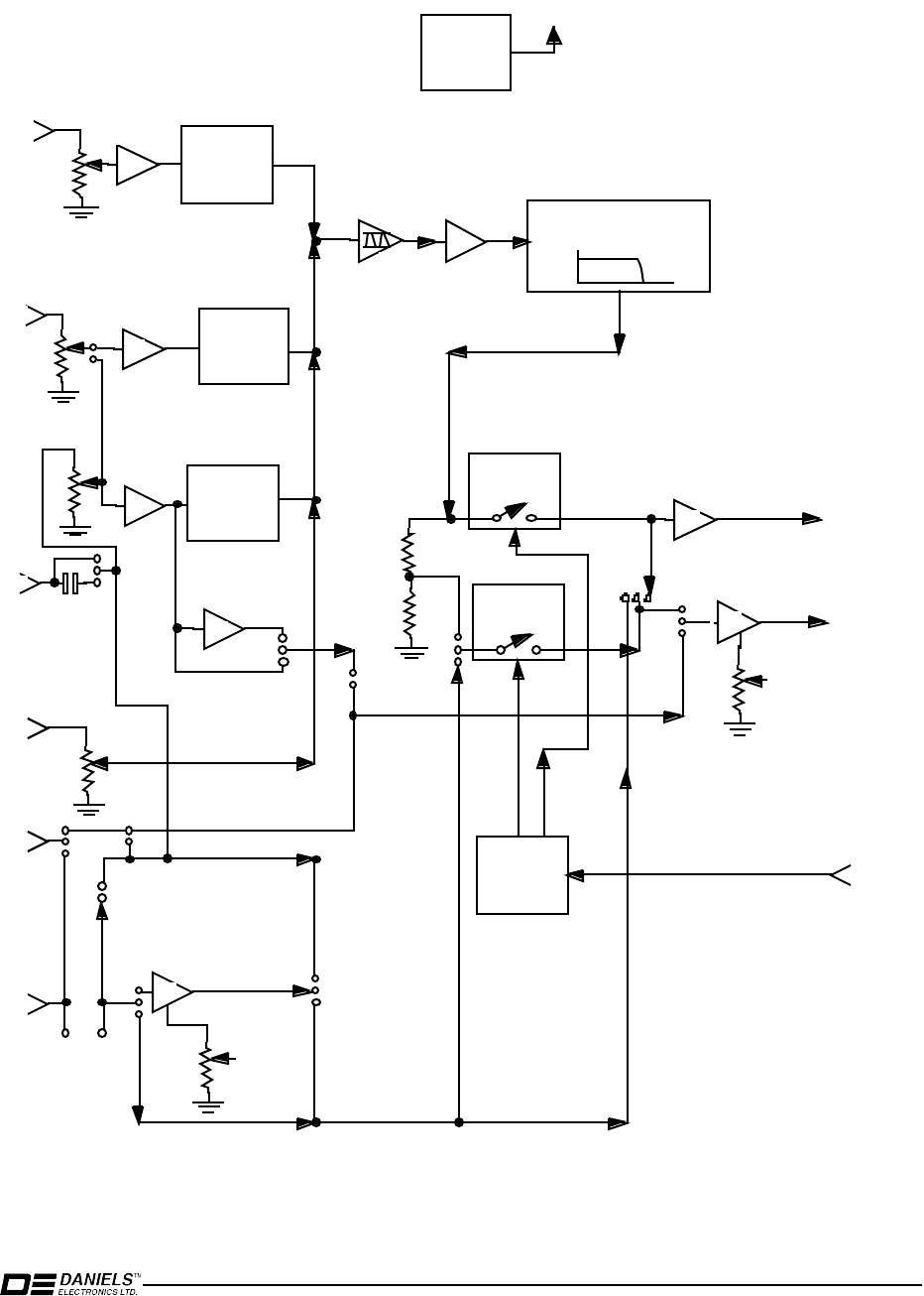
Audio Processor Board Instruction Manual 1-3
1.2 Block Diagram (FM Audio Processor)
Splatter
Filter
Pre-
emphasis
Select
Pre-
emphasis
Select
Compression
Amp
Compression
Amp
Limiter/Summing
Amplifier
Buffer
+4V
Regulator
+4V
Pre-
emphasis
Select
Auxillary
Buffer
Amp
Tx Audio
Control
Audio
Switch 1
Audio
Switch 2
Regular Modulation
Buffer
Subtone
1
3 KHz
Direct Modulation
Offset Buffer
TCVCXO
Modulation Buffer
Offset
TCVCXO
DC Level
Adjust
Reg Mod
Out
Low Freq
Out
Inverting Amp
Coupling
Select
2 Port
Polarity
Select
JU35
JU34
Tx Audio
Control
Wide/Narrow
Band Select
Data/Voice
Select
3dB
Narrow
Band
Pad
JU14
JU26
JU27
JU30
JU43
JU28
JU25
49K9
49K9
P1-3
R2
U1A
U1B
P1-1
R31
Tone
Digital
Input
P2-1
Balanced
Input
Microphone
Input
U3A
U3B
U2A
U2C
U2D
P2-2
R48
R42
U5
U6
Q1
Direct
Modulation
Input
P4-3
U2B
R87
P4-4
P4-2
P3-1
U3C
U3D
P4-1
JU4
Subtone
2
JU13
R36
JU12
JU11
Figure 1 Block Diagram - Audio Processor
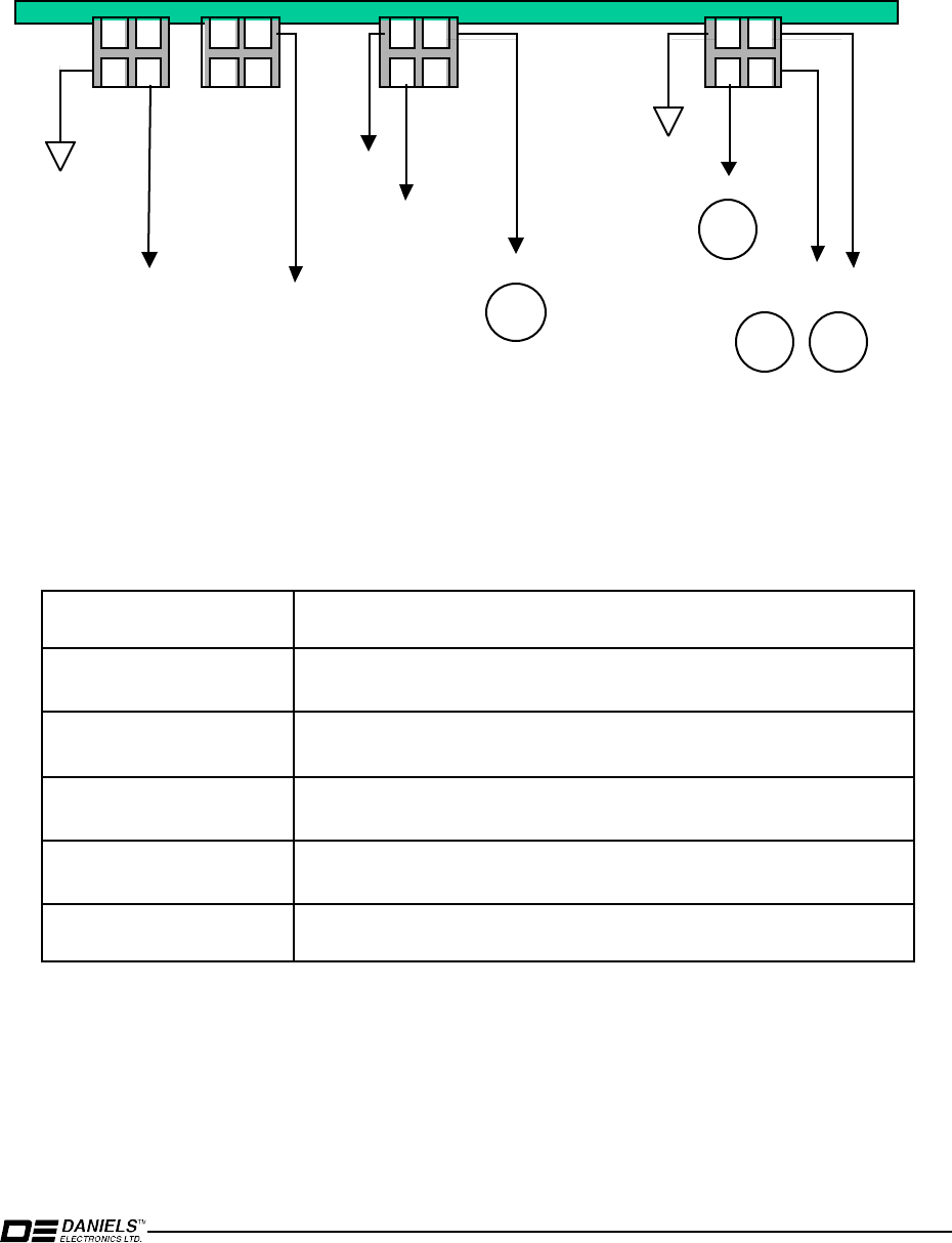
1-4 Audio Processor Board Instruction Manual
1.3 FM Audio Processor Board Pin Connections
Figure 2 Pin Connection Diagram
1.4 Factory Configuration
The MT-3 FM Audio Processor is factory configured as follows:
Table 2 Factory Configuration
Parameter Specification
Maximum Deviation
±
2.5 kHz (Narrowband),
±
5.0 kHz (Wideband).
Microphone Input 1 kHz signal at -10 dBm gives
±
60% rated system deviation
1 kHz signal compression set at
±
84% rated system deviation
Audio Balanced Input
pre-emphasis response
1 kHz tone at -8 dBm gives
±
60% rated system deviation
1 kHz signal compression set at
±
84% rated system deviation
Subtone Input 1 100 Hz tone at -18 dBm gives
±
500 Hz (Wideband)
±
350 Hz (Narrowband) deviation
All other audio inputs Disabled
P
CB
1
2
3
4
1
2
3
4
1
2
3
4
1
2
3
4
P1
P2
P4
P3
Ba
l
an
c
ed Input
E
ND V
IEW
M
i
c Input
S
ubtone Inpu
t 1
+
8V
+
9.5
V
Lo
w Fr
equen
c
y
D
i
r
e
c
t Mod
O
utput
Vo
i
c
e
An
d Subtone
O
utput
-
8
d
B
m
-
10
d
B
m
-
18
d
B
m
Su
r
fa
c
e Mount Side
0
d
B
m
Audio Processor Board Instruction Manual 1-5
1.5 Turn-on Time
This measurement is made with the standard factory settings with a 1 kHz tone applied to the
balanced input. The turn-on time is the time it takes the FM Audio Processor to output a stable
audio signal to P3-1 from the time its power (
+
8.0 VDC) is switched on.
The turn-on time can be virtually eliminated by configuring the FM Audio Processor for
continuous audio standby (see section 1.7 Transmitter Standby Modes). The drawback is that
more current is used to enable the audio circuits to minimize the turn on time. The bulk of the delay
is in the powering of the compression amplifier. For applications that do not use the compression
amplifier, the fast turn on times apply as in the case of data transmission, or audio with no
compression.
Table 3 Turn On Time
Mode Turn on time Audio Processor
Standby Current
Fast turn on – higher current Approx 1mS 15 mA
Current save – slower response Approx 150mS 450uA
1.6
L
ow Frequency Modulation
The transmitter has an additional option to address low frequency user modulation requirements. A
phase modulated bandwidth from 0 (dc) to 100 Hz (PLL loop filter bandwidth) allows specialized
applications such as paging or trunking where a separate low frequency digital/analog modulation
channel is required. Low Frequency Modulation allows external access to the low frequency
modulation capabilities of the synthesizer module. The DIRECT MODULATION inputs on the J1
control connector of the M-3 motherboard will be used (B20 for TX A, and A20 for
TX B). Refer to
“
Data Modulation and Signalling Applications Manual
”
, P/N AM20-DMS for
specific FM Audio Processor configuration methods.
1.7 Transmitter
S
tandby Modes
The MT-3 series transmitters has 8 different standby modes that trade-off standby current
consumption for start-up speed.
Three of these jumpers are on the Transmitter Main Board :
• J6 which always turns on the '
+
9.5 VDC Switched' supply,
• J7 which selects the power source for the MT-3 FM Audio Processor
• J18 which selects the enable line for the OS-3 or OS-3H Synthesizer, or OC-3 Crystal
Controlled Oscillator module.
Additionally, there is a jumper on the FM Audio Processor Board:
• JU36 which determines the power hookup for the dual compression amplifiers
1-6 Audio Processor Board Instruction Manual
Notes:
If FM Audio Processor JU36 is not installed, both microphone and balanced audio compression
amplifiers will be disabled. This means that the front panel microphone jack will be disabled for
local microphone operations. When in this condition, balanced audio is routed around the
compression circuitry via JU11 (installed) with JU1 and JU2 removed.
Table 4 Mode Condition Table
MODE
#J6
J7
J18
Synthesizer/Osc
State Audio
Processor State
(
8V Switched
)
Audio Processor
Compression
JU36
1a
OUT
Y Y
PTT Switched PTT Switched Switched
+
8.0V(X)
1b
OUT
Y Y
PTT Switched PTT Switched Continuous 9.5V(
Y
)
1c
O
UT
Y Y
PTT Switched PTT Switched
Disabled (Not Installed)
2a IN
Y
X Always enabled PTT Switched Switched
+
8.0V (X)
2b IN
Y
X Always enabled PTT Switched Continuous 9.5V (
Y
)
2c IN
Y
X Always enabled PTT Switched
Disabled (Not Installed)
3 IN X
Y
PTT Switched Always enabled Doesn
’
t matter
4 IN X X Always enabled Always enabled Doesn
’
t matter
Table 5 Standby Mode Selection Table
MODE
#Total Xmtr Standby
Current Startup Time
1a 13 mA 6 mA
150 mS
150 mS
1b 22 mA 15 mA 10 mS 10 mS
1c 13 mA 6 mA 10 mS 10 mS
2a 165 mA 25 mA
150 mS
150 mS
2b 174 mA 34 mA 10 mS 10 mS
2c 165 mA 25 mA 10 mS 10 mS
3 27 mA 20 mA 10 mS 10 mS
4 175 mA 34 mA 10 mS 10 mS
Table 6 FM Audio Processor Total Current Consumption.
Compression configuration Audio Processor
Current Draw
keyed / unkeyed
Compression enabled (JU36X) 15 mA/0.45 mA
Compression and microphone disabled
(JU36 Open)
9.2 mA/0.45 mA
Compression enabled (JU36
Y
) 15 mA /9.2 mA

Audio Processor Board Instruction Manual 2-1
2 S
I
G
NALS
The MT-3 FM Audio Processor has six audio inputs, two audio outputs and one audio control
input. Five of the audio inputs are used primarily for voice and tone signals. The sixth, the Direct
modulation input, is used primarily for data signals. The audio control input is used to switch audio
outputs so the transmitter can transmit voice or data.
2.1 FM Audio Processor Outputs
Both the audio outputs, Modulation Output (P3-1) and Low Frequency / Direct Modulation Output
(P4-2), are gated by audio switches U5 and U6 respectively which are controlled by the Transmit
Audio Control Input (P4-4). The audio switches can be operated complimentary to each other so
there can ever only be one source modulating the transmitter. In standard configuration, the
Modulation Output port is used so switch U5 is always on.
2.2 Modulation Output
The Modulation Output port is the output port used by all voice input signals. The voice inputs are
passed to U1A and U1B, a dual programmable compandor which is configured as an automatic
level control amplifier. Op-amp U3A provides the limiting action for the FM Audio Processor.
After the audio signals have been combined limited and buffered, they are filtered by 10th order
Linear Phase Lowpass Filter (U4). The output signal from the filter is then level adjusted by the
deviation control pot, R29, before buffer amplifier U3D.
In special applications, jumper JU6 can be disabled and JU7 enabled, this allows the transmitter to
be modulated directly from the auxiliary input. This should not be done without external filtering
since jumper JU7 bypasses the limiting and filter circuits.
2.3
L
ow Frequency / Direct Mod. Output
The Low Frequency / Direct Modulation Output port has two functions depending on whether the
transmitter is synthesized or crystal controlled. In a synthesized transmitter, this port is used to
modulate the synthesizer reference frequency. The frequency response of this port is typically DC
to 300 Hz. In a crystal controlled transmitter, this port can be used by the Direct Modulation Input
to directly modulate the crystal control oscillator module. The frequency response of this port is
essentially flat from DC to 5 kHz with no limiting or filtering.
2.4 Microphone Input
The microphone input has an automatically level controlled (ALC) preamplifier U1 whose input
level is controlled by R2. The microphone input level control (R2) can accommodate a -25 dBm to
0 dBm input signal. The microphone input is limited and filtered and is output at the standard
modulation output port. The microphone input can have a standard 6dB/octave pre-emphasis
response or a flat-audio response, jumper JU1 at 'y' and 'x' position respectively.
2.5 Balanced Input
The 600 ohm balanced input uses the ALC preamplifier U1B, with input level control pot (R31).
The balanced input level control can accommodate a -25 dBm to 0 dBm input. (install JU17 when

2-2 Audio Processor Board Instruction Manual
using the lower input levels) Like the microphone input, the balance input is limited and filtered and
is output at the standard modulation output port.
If no compression is required (i.e.: customer is providing their own), JU11 can be enabled
providing a path through R48 (Auxiliary Input Level Control) to amplifier U2C where pre-
emphasis or flat audio can then be selected from its output.
2.6 Auxiliary Input
The auxiliary input is a special input and does not have an ALC. This input can be configured for a
pre-emphasis response (enable JU9
Y
) or a flat-audio response (enable JU9X). The level for this
input is set by R48. The auxiliary output is normally summed with the voice signals by op-amp
U3A, limited, then filtered and output at the standard modulation output port. When jumper JU6 is
disabled and jumper JU7 is enabled, the auxiliary input can be used to directly modulate the
transmitter. Care should be taken when directly modulating the transmitter with the auxiliary input
because the MT-3 transmitters use direct FM modulation and there is no filtering or limiting action
provided by the auxiliary input. The input level to the auxiliary input should be -18 dBm and can
be driven by one of three inputs:
• the balanced input – JU11
• the tone/digital input – JU12 X or
Y
enabled
• the direct modulation input – through JU28
When the 600 ohm balanced input is connected to the auxiliary input, the balanced input level
control can be used to adjust the level for the auxiliary input.
2.7
S
ubtone Inputs
There are two subtone inputs available on the FM Audio Processor. Both subtone inputs can be
individually configured to be output from the standard Modulation Output port or to be output from
the Low Frequency / Direct Modulation Output. In standard configuration, Subtone 1 is summed
with the voice signals to be output from the standard Modulation Output port while Subtone 2 is
used for DCS. Both subtone inputs have an input level control.
2.8 Direct Modulation Input
The Direct Modulation Input is an extremely versatile input. This port is designed to be used for
data signals. Depending on the application, the signal can be amplified, AC or DC coupled and
output to the Modulation Output or the Low Frequency / Direct Modulation Output port. Please
consult the factory for specific jumper settings for your application.
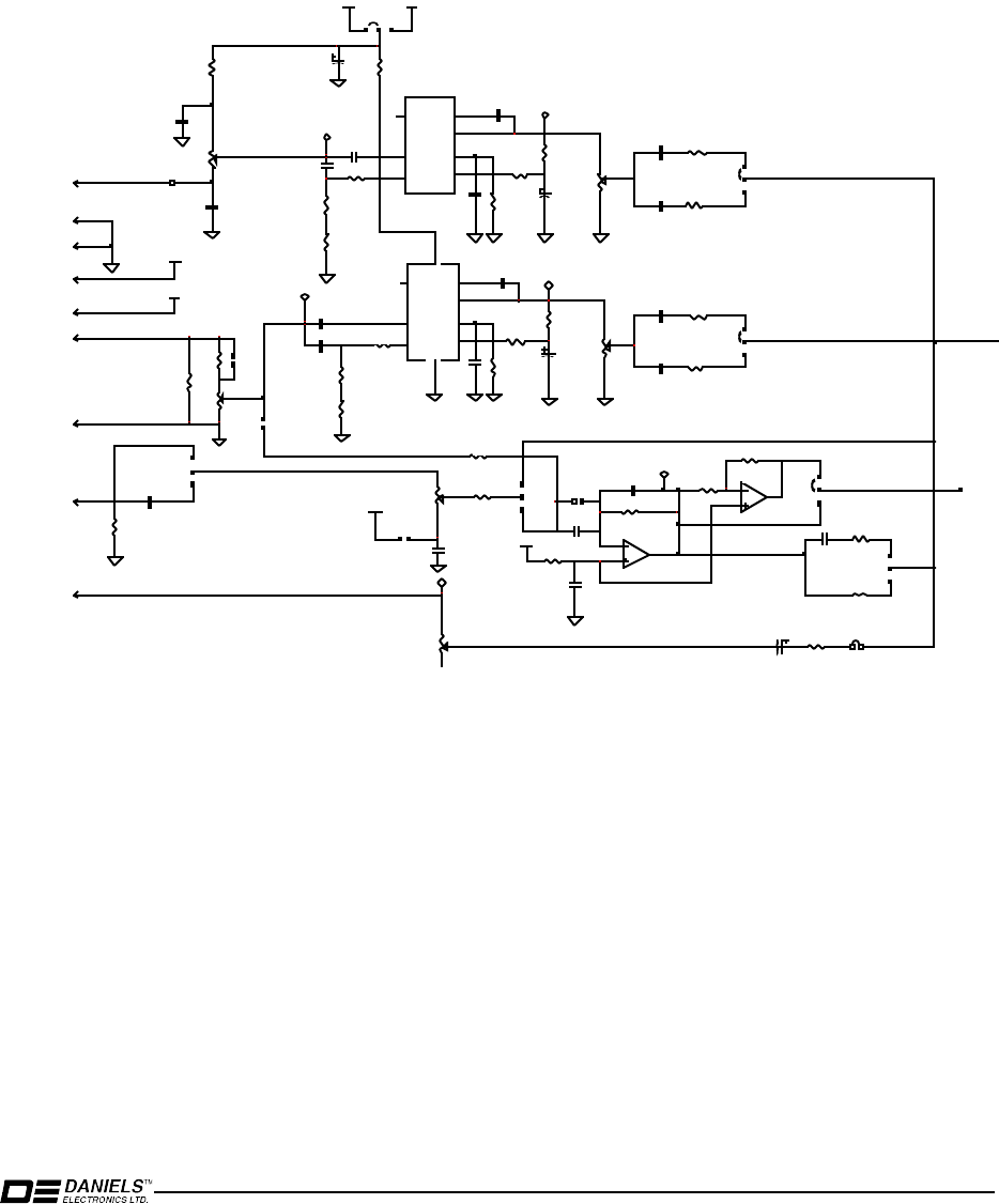
Audio Processor Board Instruction Manual 3-1
3 T
H
E
OR
Y
OF OP
E
RAT
I
ON
Voice band audio normally enters the Balanced Input at P1-1 and P1-2 while microphone audio
enters at P1-3. Potentiometer R31 sets the Balanced compression level of U1B while R2 sets the
microphone compression level of U1A. Each amplifier has a dynamic range of 25 dB. Jumper
JU17 is only installed when using very low input levels (-20 to –25 dBm) and allows better tuning
range for R31. The output of the compression amplifiers are normally set for Pre-emphasis
(6dB/Octave) but can be set for flat audio if required by jumpers JU1 and JU2.
BA
L
AN
C
E
D
I
N
P
U
T L E
V
E L
C
O
N
T
R
OL
F
LAT
A
UDI
O
P
R
E-
E
M
PHASIS
MI
CR
OP
H
O
N
E
I
N
P
U
T
L E
V
E L
C
O
N
T
R
OL
BALANCE
D
INP
U
T
X
Y
+
9
.5V C
O
NTI
NU
O
US
N
O
T INSTAL
L
E
D
F
O
R
DI
G
ITAL
M
O
D
.
A U
X
ILI
AR
Y I
N
P
U
T
L
E
V E L
C
O
N
T
R
OL
X Y
MI
C
R
O
P
H
O
N
E
A
G
C
P
R
E
A
M
P
B A
L
A N
C
E
D
A
G
C
P
R
E
A
MP
X
Y
B A
L
A N
C
E
D
C
O
MP
R
E
SSI
O
N
C
O
N
T
R
O
L
FLAT AUDI
O
P
R
E
-
E
M
PHASIS
MI
CR
O
P
H
O
N
C
OMP
R
E
SS
I
C
O
N
T
R
OL
X
Y
X
Y
X
Y
FLAT
A
UDI
O
PRE-E
M
PHASIS
X
Y
TW
O
P
O
RT P
O
LARITY
S
U
B
TO
N
E 1 I
N
P
U
T
C
O
N
T
R
OL L
E
VEL
3
P1
2
P1
1
P1
4
P1
3
P3
3
P2
1
P2
4
P2
+9.5V CONTINUOUS
C10
10nF
4K53
R46
C5
10nF
1
2
3
R2
5K0
FB1
+8.0V SWD
+8.0V SWD
1
2
3
JU5
47uF
C13
3
2
1
100K0
R48
680nF
C7
4.7uF
C8
TP3
SEL
R57
N/I (22nF)
C32
Rect In
Var G
Rect Cap
Output
Inv In
R3
THD
Trim
15
14
16
10
12
11
9
U1
SA571D
a
680nF
C42
TP12
4.7uF
C26
Vcc
Rect In
Var G
Rect Cap
Output
Inv In
R3
THD
Trim
GND
2
3
1
7
5
6
8
13
4
SA571D
U1
b
2
P2
JU16
9
10
8
U2
MC33174
c
R74
N/I
R73
N/I
13
12
14
U2
MC33174
d
4.0V
TP6
R43
11K8
C39
2.2uF
3
2
1
5K0
R42
C35
1.0uF
C1
1.0uF
C9
1.0uF
C30
1.0uF
R82
10K0
C37
3.3nF
R49
16k2
C14
10nF
4.0V
R76
16k2
C16
1.0uF
JU33
C51
1.0uF
1
2
3
JU12
R39
15K4
R41
137K
R59
20K0
R62
15K4
R5
1M00
C25
1.0uF
R60
18K2
R61
18K2
R8
2K21
R9
49K9
R4
18K2
R6
18K2
330nF
C36
C15
3.3nF R7
2K21
R10
49K9
330nF
C19
C2
1.0uF
R51
10K0
2
1
3
JU1
2
1
3
JU2
JU11
TP11
TP4
JU10
R52
100K
R65
100K
C38
3.3nF
R11
2K21
R40
49K9
2
1
3
JU14
1
2
3
R31
5K0
R30
604R
TP2
215R
R1
R64
100K
R56
0R0
C4
1.0uF
2
3
1
JU36
JU17
1
2
3
JU9
1
2
3
5K0
R63
3
2
1
5K0
R38
MICROPHONE INPUT
SUBTONE INPUT 1
TONE/DIGITAL I/P
Figure 3 Microphone and Balanced Input Circuitry
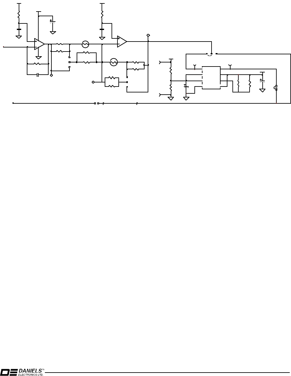
3-2 Audio Processor Board Instruction Manual
The microphone and balanced audio signals are summed and limited by U3A. Op-amp U3B
provides audio level temperature compensation (for synthesizer and crystal oscillator sensitivity
variations). Due to the many different characteristics of the models of synthesizer and crystal
oscillators, the components are marked
“
SELect
”
and are identified later in this document (section
6.)
XY
X
Y
X
Y
1
0
P O
L
E
L
O
W
P
AS
S
F
I
L
T
ER
L
IM
I
T
E
R
T EMPE
R
AT
U
R E
C
O
MPE N S ATI
O
N
213
JU22
R16
100K
C17
10nF
C49
10nF
+8.0V SWD
JU6
C50
4.7uF
JU7
SEL
R23
SEL
R24
SEL
R25
SEL
R26
SEL
R28
SEL
R17
SEL
R18
SEL
R20
In+
In-
Gnd
V-
Vout
V+
Rx
Div/Clk
1
2
3
4
8
7
6
5
U4
LTC1569-6
R66
22K1
R67
30K9
R68
3K48
R69
2K00
+8.0V SWD
P11
P12
P9 P10
2
34
1
11
U3
MC33174
a
6
57
U3
MC33174
b
1
2
R19
SEL
1 2
SEL
R27
1
2
C21
1.0uF
1
2
C6
1.0uF
4.0V
4.0V
+8.0V SWD
TP5
R84
10K0
R85
10K0
TP10
1 2
150pF
C43
TP14
1
2
3
JU24
1
2
3
JU3
Figure 4 Limiter and Splatter Filter
The audio then is filtered by a 10th Order Linear Phase Lowpass splatter filter. This filter improves
on the previous Butterworth filter design for data linearity and increased cutoff attenuation
responses mandated in today
’
s narrow band environment.
The filter output level is set by R29, the deviation control. From this point, the signal goes to U5 a
bilateral audio switch. U5 is normally configured to be always on. The output of U5 goes to the
final buffer amplifier U3D. By installing JU23 which lowers the audio level one half, a wideband
transmitter can be quickly re-configured into a narrowband transmitter in the field. The output of
U3D has many selectable capacitors which are chosen depending on the synthesizer or crystal
oscillator module that is connected to this main modulation port.
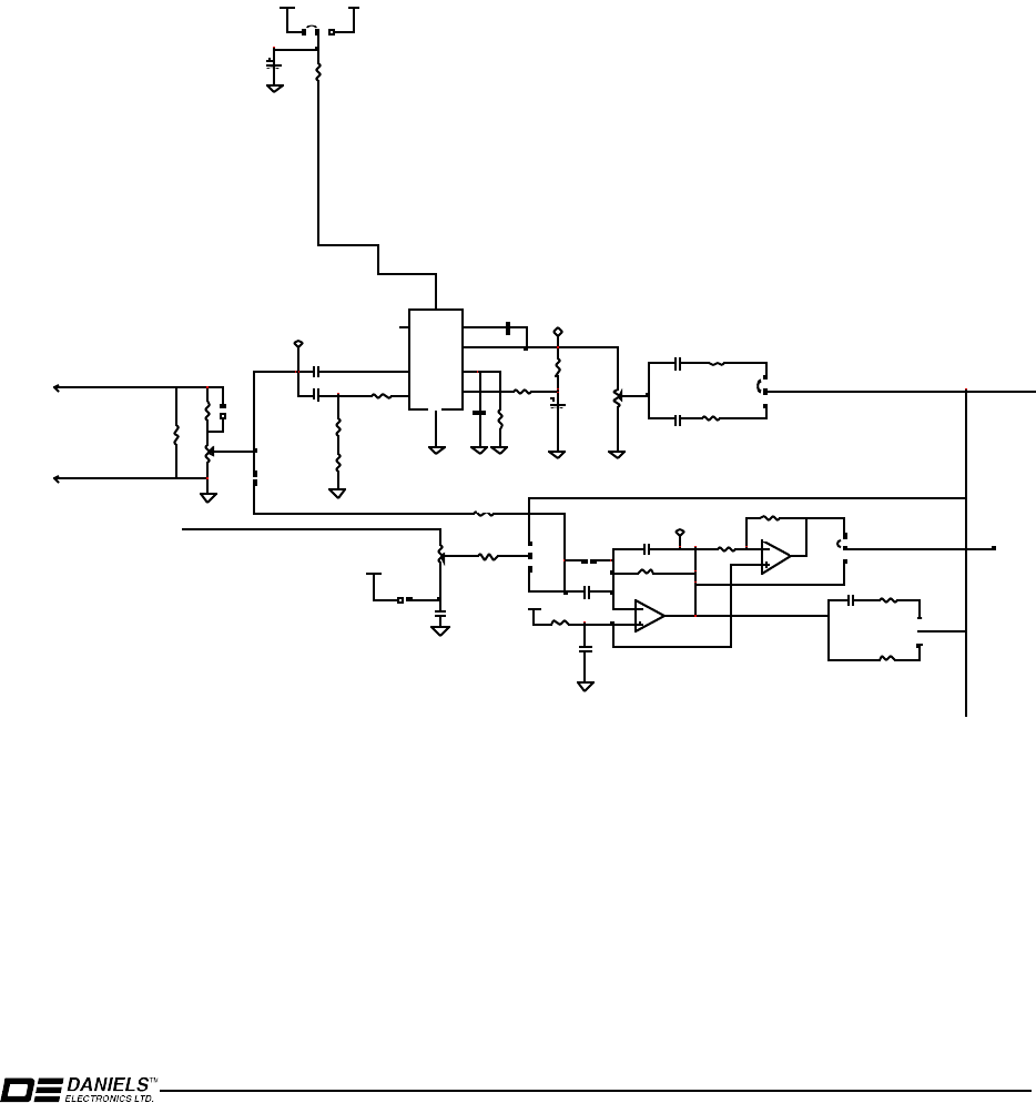
Audio Processor Board Instruction Manual 3-3
If no compression circuitry is required, the balanced input signals can be routed around the
compression circuitry by jumper JU11. Op-amp U2C then would provide the
buffering/amplification. It
’
s output would normally have pre-emphasis installed but could be
changed to flat if required through jumper JU9. The audio signal is then normally routed to U3A,
the summing amplifier/limiter and processed as mentioned in the previous paragraphs. Note
however, if compression is bypassed, the THD may be higher due to the reduced dynamic input
range causing more clipping.
If compression is bypassed and disabled by the removal of FM Audio Processor jumper JU36
which removes power from the compression IC, there will be 9mA of key down current saved. The
disadvantage is that the microphone circuit will be disabled due to the removal of the common
power to the compression IC.
BA
L
ANC
E
D
I
N
P
U
T L
E V
E
L
C
O
N
T
R
O L
B
A
L
A
NCED INPUT
X
Y
A
U
X
ILI
AR
Y
I
N
P
U
T
L
E
V E
L
C
O
N
T
R
O L
BA
L
ANC
E
D
A
G
C
P
R
E
A
M
P
B
A
L
AN
C
E
D
C
OM
P
R
ESS
I
O
N
C
O
N
T
R
O
L
FLAT
A
UD
I
O
PRE-EMPHASIS
X
Y
X
Y
FLAT AUDI
O
PRE-EMPHASI S
X
Y
TW
O
P
O
RT P
O
LA
R
I
T
Y
2
P1
1
P1
C10
10nF
1
2
3
JU5
3
2
1
100K0
R48
680nF
C7
4.7uF
C8
TP3
SEL
R57
N/I (22nF)
C32
Vcc
Rect In
Var G
Rect Cap
Output
Inv In
R3
THD
Trim
GND
2
3
1
7
5
6
8
13
4
SA571D
U1
b
9
10
8
U2
MC33174
c
R73
N/I
13
12
14
U2
MC33174
d
4.0V
TP6
C9
1.0uF
C30
1.0uF
R82
10K0
R49
16k2
C14
10nF
4.0V
R76
16k2
C16
1.0uF
JU33
R62
15K4
R5
1M00
R4
18K2
R6
18K2
C15
3.3nF R7
2K21
R10
49K9
330nF
C19
C2
1.0uF
R51
10K0
2
1
3
JU2
JU11
TP4
JU10
R52
100K
R65
100K
C38
3.3nF
R11
2K21
R40
49K9
2
1
3
JU14
1
2
3
R31
5K0
R30
604R
R64
100K
JU17
1
2
3
JU9
3
2
1
5K0
R38
+9.5V
C
O
N
TIN U
O
US
X
Y
M
+8.0V SWD
R56
0R0
2
31
JU36
Figure 5 Bypassing Compression
A second way to route around audio compression if data is not being used is to use the direct
modulation port P4-3 and go through JU28 to R48 and Op-amp U2C.
Subaudible tones enter at P2-2 where their level is controlled by R42. A single jumper JU16
enables the audio path to U3A, the summing amplifier/limiter.
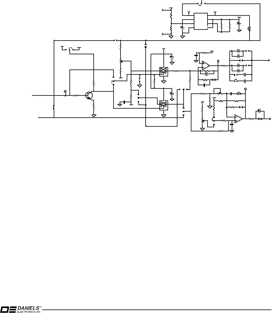
3-4 Audio Processor Board Instruction Manual
Voltage regulator U2A provides regulated
+
4.0V to all Op-amp stages. Optional potentiometer R14
can be installed (and JU15 removed) for special applications which need a voltage different than
+
4.0V.
Data normally enters at P4-3, the Direct Modulation Input. From there, it has many routes that it
can go. JU43 allows direct or on-board capacitive coupling. Op-amp U2B can be configured as a
buffer with a DC offset to handle input data that has a positive DC voltage offset. The data signals
can be sent to gain buffers U2C and U2D through potentiometer R48. Jumper JU14 is normally
installed so that the output from U2D provides the correct data polarity when using two port
modulation.
X
Y
D
E
V
I
A
TIO
N
C
O
N
T
R
O
L
L
O
W FRE
Q
U
ENCY /
D
IRECT
M
O
DULATI
O
N
O
UTPUT
X
Y
X
Y
X
Y
X
Y
V
O
I
C
E
+ SUBA
U
DIBLE
D
C
S
, LTR
X
Y
T
C
X
O
D
C
L
EV
E
L
A D
J
U
S
T
T
C
X
O MO
D U
L
A
TIO
N
L
E
VE
L
A D
J
U
S
T
1
P3
2
P4
JU37
2
13
JU22
+9.5V CONTINUOUS
4.7uF
C45
4.7uF
C28
1
2
3
R29
50K0
R55
49K9
R75
10K0
E
B
C
Q1
BC817-25
+8.0V SWD
JU6
JU31
R44
0R0
R45
N/I
C12
1.0nF
R54
SEL
1
2
3
R36
50K0
JU32
SEL
R32
JU29
47uF
C34
R12
N/I
R79
49K9
JU7
In+
In-
Gnd
V-
Vout
V+
Rx
Div/Clk
1
2
3
4
8
7
6
5
U4
LTC1569-6
R66
22K1
R67
30K9
R68
3K48
R69
2K00
+8.0V SWD
P11
P12
P9 P10
9
10
8
U3
MC33174
c
0R0
R72
0R0
R58
1
2
C21
1.0uF
1
2
C6
1.0uF
R37
49K9
R34
49K9
4.0V
C24
10nF
+8.0V SWD
4.0V
JU23
TP7
TP8
TP9
SEL
R81
JU41
10nF
C41
R86
10K0
3
2
1
R83
50K0
R53
N/I
R80
27K4
+8.0V SWD
1
2
3
JU35
R78
10K0
2
3
1
JU39
1
2
3
JU34
JU38
C23
330pF
C44
330pF
13
12
14
U3
MC33174
d
R35
SEL
JU8
100nF
C27
1.0uF
C33
1.0uF
C40
1.0uF
C47
1.0uF
C46
1
2
3
JU25
R22
49K9
R21
49K9
1 2
3
4
5
U5
TC4S66F
1 2
3
4
5
U6
TC4S66F
4.0V
R50
49K9
R88
49K9
JU26
4.0V
C55
100nF
JU44
33nF
C56
+9.5V CONTINUOUS
R77
20K0
JU18
2
1 3
JU19
2
3
1
JU21
1 2
JU45
R89
100R
Tx Audio Control
Figure 6 TX Audio Control Circuitry
A single TX Audio control line P4-4 has 2 functions. It can be configured to switch U3D inputs
between data and voice. Alternately, it can be configured to remotely switch between wideband and
narrowband applications by switching between the regular audio path and one carrying half the
audio level as determined by resistive divider comprised of R22 and R21.
Due to the complex nature of data modulation methods, the actual configurations and values of
SELected components for LTR, DCS, Paging are contained in a separate applications manual
“
AM20-DMS
”
.

Audio Processor Board Instruction Manual 4-1
4 AL
I
G
N
M
E
NT
Verify the standard factory settings for the MT-3 FM Audio Processor as given in section 1 before
beginning the standard deviation adjustment procedure. If the transmitter's operating frequency is
changed beyond the factory recommended bandwidth or if the synthesizer is changed, the FM
Audio Processor should be realigned to optimize the transmitter's performance. The schematic
diagram for the FM Audio Processor is shown in section 7-2 of this manual.
The settings tolerance is
+
/- 0.1 kHz.
4.1
S
tandard Deviation Adjustment
Set up the Communications Analyzer :
-Audio filter to LOW PASS 15 or 20 kHz
-To monitor transmit frequency and audio deviation level.
4.2 Balanced Input
S
etup
1 Connect audio generator output to the BALANCED INPUT (Transmitter
Main Board edge connector pins B18, Z18).
2 Preset R31 (BALANCED INPUT LEVEL CONTROL)
R38 (COMPRESSION CONTROL)
R29 (DEVIATION CONTROL)
all maximum clockwise
3 Set audio generator to 2.4 kHz at 0 dBm.
4 Adjust R29 for
±
4.8 kHz (Wideband) or
±
2.4 kHz (Narrowband).
5 Set audio generator to 1 kHz at 0dBm
6 Set R38 for
±
4.2 kHz (Wideband) or
±
2.1 kHz (Narrowband).
7 Repeat steps c) to f) (slight interaction)
8 Set audio generator to 1 kHz at –8 dBm
9 Adjust R31 for
±
3.0 kHz (Wideband) or
±
1.5 kHz (Narrowband).
10 Set audio generator to 1 kHz at –18 dBm
11 Ensure deviation is at
±
1.0 kHz (Wideband) or
±
0.5 kHz (Narrowband).
12 Set audio generator to 1 kHz at –8 dBm. Set Communications Analyzer Audio
Filter to BANDPASS 300-3400 Hz. Activate distortion analyzer. Confirm that
the distortion is within specification.
4.3 Microphone Input
S
etup
1. Set R2 fully clockwise
2. Apply a 1 kHz tone at 0 dBm to the microphone audio input (PIN 1 on the front
panel connector. Pin 2 is ground). Set R63 (MICROPHONE
COMPRESSION for
±
4.2 kHz (Wideband) or
±
2.1 kHz (Narrowband).
3. Reduce the audio generator level to –10 dBm. Adjust R2 (MICROPHONE
INPUT LEVEL) for
±
3.0 kHz (Wideband) or
±
1.5 kHz (Narrowband).

4-2 Audio Processor Board Instruction Manual
4.4
S
ubtone Input
S
etup
• Apply a 100 Hz tone at -18 dBm to the subtone 1 input .
• Adjust R42 (SUBTONE INPUT 1) to produce:
•
±
500 Hz(Wideband) or
±
350 Hz(Narrowband) deviation.
• Remove the signal.
4.5 Balanced Input Frequency Response
• Apply a 1 kHz tone at –18 dBm to the BALANCED INPUT (Transmitter Main
Board edge connector pins B18, Z18).
• Record deviation and use this level as the 0 dB reference.
• Sweep frequency from 100 Hz to 5 kHz.
• The audio response should be within
+
/- 1dB from 300 Hz to 2500 Hz.
Audio Processor Board Instruction Manual 5-1
5 TRO
U
BL
E
S
H
OOT
I
N
G
- T
E
ST
E
Q
U
I
P
M
E
NT N
EE
D
E
D
1 Variable Power supply/supplies to supply 9.6V and 8.0V at the same time.
2 Digital Voltmeter to measure RMS AC Volts, DC Volts, DC Current and resistance.
3 20 MHz Oscilloscope, single channel.
4 Audio Signal Generator (600 Ohm Output Impedance) capable of frrequencies from
67 Hz to 5000 Hz.
Power Supply
• Connect a regulated power supply with
+
9.5V as follows:
Positive to P2-4
Negative to P1-4 (Ground)
• Connect a regulated power supply with
+
8.0V as follows:
Positive to P2-3
Negative to P1-4 (Ground)
• Measure total current from both power line inputs:
Table 7 Operating Current
Voltage Input
Current
(
mA
)
8.0V 15.7
9.5V 0.47
5.1 Balanced Input Test
Connect an Audio Generator set for a 2.4 kHz tone @ 0 dBm (775 mV RMS) output to the
Balanced Input (P1-1 and P1-2). Refer to Table 8 Waveform Levels for measurement points,
levels and waveforms that should be present.
Change Audio Generator settings for a 1 kHz tone @ -8 dBm (309 mV RMS) output. Refer to
Table 8 Waveform Levels for levels and waveforms that should be present.
5.2 Frequency Response Test
Reduce Audio Generator level to –18 dBm (98 mV RMS). Step frequency to 500, 1000, 2000 and
3000 Hz. Ensure that the results conform to the 6dB/octave
+
/- 1 dB from 300 Hz to 2500 Hz
referenced to 1000 Hz. Measurements are made at JU8 with respect to ground.
5-2 Audio Processor Board Instruction Manual
5.3
S
ubtone Input Test
Change Audio Generator frequency to 100 Hz and maintain level at –18 dBm (98 mV RMS).
Connect output to Subtone Input 1 (P2-2) and ground (P1-4). Refer to Table 8 Waveform
Levels, for levels and waveforms that should be present.
5.4 Audio benchmarks
Set the audio generator to 2.4 kHz @ 0 dBm at the Balanced Input. Compare the waveform levels
with those listed in table below.
Repeat for the various audio frequencies and levels and compare with the levels in the table below.
Table 8 Waveform Levels
Limiting Test
Std Level Mic Test Subtone
Measured
@
2.4kHz
@0dBm
1 kHz @
-8dBm
1 kHz @
-10 dBm
100 Hz @
-18 dBm
TP3 5.2V P-P 3.8V P-P N/A N/A
TP12 N/A N/A 3.8V P-P N/A
TP10 6.5V P-P 4.9V P-P 4.8V P-P 1.1V P-P
TP5 2.4V P-P 1.3V P-P 1.9V P-P 0.4V P-P
JU6 5.5V P-P 1.7V P-P 1.8V P-P 0.4V P-P
TP8 1.5V 0.9V P-P 0.9V P-P 0.2V P-P

Audio Processor Board Instruction Manual 6-1
6 T
E
M
P
E
RAT
U
R
E
CO
M
P
E
NSAT
I
ON
The FM Audio Processor includes temperature compensation circuitry to maintain constant
transmitter audio deviation with a fixed level input signal. It is capable of not only compensating for
temperature related level variations within the FM Audio Processor (typically –0.3 to –0.5 dB at
–40C) but can also compensate for changes caused by the synthesizer or crystal oscillator module
that is not equipped with its own temperature compensation.
The factory specification is as follows:
Wideband
When a 2.4 kHz tone is applied at a level of –8dBm to the balanced input of the transmitter, the
transmitter deviation shall be
±
4.8 kHz at room temperature and can vary from
±
4.5 kHz to
±
5.0 kHz from -40ºC to
+
60ºC.
Narrowband
When a 2.4 kHz tone is applied at a level of –8 dBm to the balanced input of the transmitter, the
transmitter deviation shall be
±
2.4 kHz at room temperature and can vary from
±
2.25 kHz to
±
2.5 kHz from -40ºC to
+
60ºC.
Since the specifications of the components used in the synthesizer or oscillator may change over
time, changes to the temperature compensation circuit may be necessary even for the same type of
equipment.
Contact the factory for more information on values used.

6-2 Audio Processor Board Instruction Manual
This Page Intentionally Left Blank
ELECTRONICS LTD.
DANIELS TM
Audio Processor Board Instruction Manual 7-1
7 ILLUSTRATIONS, TABLES AND SCHEMATIC DIAGRAMS
7.1 Special Jumper Configuration Table
WB VHF/CTCSS
WB UHF/CTCSS
NB VHF/CTCSS
NB UHF/CTCSS
TCXO Op Amp
R35
Not Installed
O Ohms
Not Installed
0 Ohms
R32
Not Installed
51K Ohms
Not Installed
51K Ohms
R81
Not Installed
51K Ohms
Not Installed
51K Ohms
R54
Not Installed
100 Ohms
Not Installed
100 Ohms
Auxiliary Op Amp
R57
Not Installed Not Installed Not Installed Not Installed
WB VHF
WB UHF
NB VHF
NB UHF
Default
& CTCSS & CTCSS & CTCSS & CTCSS
Jumper
Type
Position
Description
1
XY
Y
Microphone Pre-Emphasis/Flat Audio
Y Y Y Y
2
XY
Y
Balanced Audio Pre-Emphasis/Flat Audio
Y Y Y Y
3
XY
Factory
Custom Temperature Compensation Network
Contact Factory Contact Factory Contact Factory Contact Factory
4
XY
Open
Subtone 2
5
XY
Open
Auxiliary Input routing
6
Single
In
Splatter Filter Output
Installed Installed Installed Installed
7
Single
Open
Auxiliary Input routing
8
Single
Open
Direct Coupled final OP Amp O/P
9
XY
Open
Auxiliary Output for Pre-Emphasis
Not Installed Not Installed Not Installed Not Installed
10
Single
Open
4V AC Ground
Not Installed Not Installed Not Installed Not Installed
11
Single
Open
Balanced Input Compression Bypass
12
XY
Open
Tone/Digital Input audio routing
13
Single
Open
Direct Modulation Audio Routing
14
XY
Y
Two Port Polarity Select
Y default OK Y default OK Y default OK Y default OK
15
XY XY
4V Regulator adjust (Bypassed)
X and Y both X and Y both X and Y both X and Y both
16
Single
In
Subaudible Enable
Installed Installed Installed Installed
17
Single
Open
Balanced Input Adjust Range extend
18
Single
Open
Audio Gate disable
19
XY
Y
Voltage Select (+9.5V/8V) Audio gates
Y Y Y Y
20
XY
Open
Direct Modulation Audio Routing
21
XY
X
Audio Gate Switch
X X X X
22
XY
Y
Splatter Filter Enable/Bypass
Y Y Y Y
23
Single
Open
Narrow Band gain reduction
Not Installed Not Installed
Installed Installed
24
XY
Factory
Custom Temperature Compensation Network
Contact Factory Contact Factory Contact Factory Contact Factory
25
XY
Open
Wide/Narrow Band switched select
Not Installed
X
Not Installed
X
26
Single
Open
Auxiliary output routing
Not Installed Not Installed Not Installed Not Installed
27
XY
Open
Direct Modulation Input Offset Output
28
Single
Open
Direct Modulation Input Routing
Not Installed Not Installed Not Installed Not Installed
29
Single
Open
Coupling Capacitor selection
Not Installed Not Installed Not Installed Not Installed
30
N/A N/A
This skipped designator has been deleted
31
Single
Open
Splatter Filter output routing
Not Installed
Installed
Not Installed
Installed
32
Single
Open
Coupling Capacitor selection
Not Installed Not Installed Not Installed Not Installed
33
Single
Open
Direct Input Coupling - Auxiliary amplifier
Not Installed Not Installed Not Installed Not Installed
34
XY
Open
Audio Routing
35
XY
Open
Audio Routing
Not Installed
X
Not Installed
X
36
XY
X
AGC Preamp Power select
X X X X
37
Single
Open
Direct Couple (TCXO)
Not Installed
Not installed
38
Single
In
Low pass enable
Installed Installed Installed Installed
39
XY
X
Low Frequency amplfier bias select
X X X X
40
N/A N/A
This skipped designator has been deleted
41
Single
Open
Narrow Band gain reduction
Not Installed Not Installed
Installed Installed
42
XY
Open
Direct Modulation input bias select
43
Single
Open
Direct Modulation Direct/Cap couple
44
Single
Open
Coupling Capacitor selection
45
Single
In
Coupling Capacitor selection (Default)
Installed Installed Installed Installed
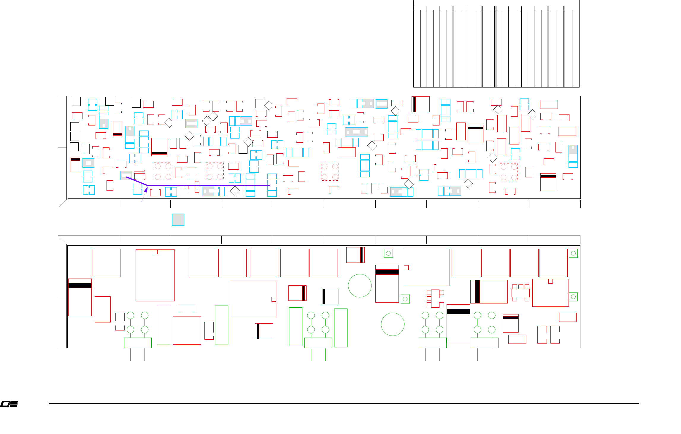
VICTORIA B.C .
DANIELS
ELECTRONICS
DRAWN BY: SHANE A
DWG REV DATE: OCT 27/00
DATE: MAR 27/00
DWG No: 9119ASx
TITLE: AM TRANSMITTER
D
TITLE: AM TRANSMITTER SURFACE MOUNT LAYOUT TITLE: FM TX AUDIO PROCESSOR BOARD OUTLINE
ELECTRONICS
PCB 43-911923
BOTTOM SIDE
TOP SIDE
TITLE: FM TX AUDIO PROCESSOR SM LAYOUT
DWG No: 9119AS1
- JUMPERS INSTALLED
TITLE: FM TX AUDIO PROCESSOR SM LAYOUT / JUMPERS
JU41 JU4
JU17 JU36
JU2X Y
X
Y
JU14
Y X
JU20
X Y
JU27X Y
JU5
Y
X
JU1
X Y
JU15
XY
JU12
XY
JU9
X
Y
X
JU39
YX
JU35
Y
X
JU34
Y
X
JU21
XY
X
JU25
Y
X
JU19
X
Y
JU22
Y
X
JU6
JU8
JU32
JU31
JU18
JU37
JU38
JU29
JU7
JU23
JU28
JU13
JU10
JU16
JU33
JU11
JU42X Y
JU43
Y
X
JU44
JU45
JU26
DWG No: 9119AS2B
JU3
Y
Y JU24
C8
4.7µF
P1
C26
4.7µF
R73
N/I
R6
18k2
R4
18k2
R56
0R0
C5
10nF
R1
0R0
C4
1µF
R5
1M0
R64
100k
R30
604R0
R74
N/I
R7
2k21
P2
C10
10nF
R11
2k21
R10
49k9
R8
2k21
R57
SEL
R40
49k9 R52
100k
R26
SEL
R25
SEL
R49
16k2
R15
10k0
C20
10nF
C36
330nF
R13
10k0
R20
SEL
R28
SEL
R81
SEL
P4
C18
100nF
C17
10nF
R17
SEL
R18
SEL
R34
49k9
C23
330pF
R16
100k0
C41
10nF
R45
N/I
R44
0R00
R53
N/I
R32
SEL
R54
SEL
C12
1.0nF
R50
49k9
C24
10nF
C45
4.7µF
R35
SEL
R12
N/I
R79
49k9
R22
49k9
R21
49k9
R55
49k9
C6
1µF
C21
1µF
P3
R58
0R00
R72
0R00
R37
49k9
R77
20k0 R75
10k0
Q1
BC817-25
R68
3k48
R69
2k00
R66
22k1
R67
30k9
C3
4.7µF
R63
5K0
U4
LTC1569-6
R42
5k0
R2
5K0 R31
5K0
R38
5K0
R48
100K0 R14
N/I (5K0) R29
50k0
U3
MC33174
R36
50k0
FB1
U5
TC4S66F
U1
SA571D
C13
47uF
C29
47uF
C31
47uF
C34
47uF
U2
MC33174
U6
TC4S66F
TITLE: FM TX AUDIO PROCESSOR SM DESIGNATIONS
R83
50k0
C48
4.7µF
C50
4.7µF
C42
680nF
C7
680nF
R23
SEL R24
SEL
R85
10k0
R78
10k0
C49
10nF
R86
10k0
C27
100nF
R9
49k9 R65
100k
R71
5k11
R46
4k53
C14
10nF
C43
150pF R84
10k0
R82
10k0
C19
330nF
R43
11k8
R47
100k R3
100k
R33
100k
R59
20k
R41
137k
R51
10k0
R62
15k4
R76
16k2
C1
1µF
C30
1µF
C9
1µF
C2
1µF
C25
1µF
C35
1µF
C39
2.2µF
R39
15k4
R60
18k2
R61
18k2
R80
27k4
C28
4.7µF
C51
1µF
C16
1.0µF
C46
1.0µF
C47
1.0µF
C33
1.0µF
C22
10nF
R70
10k0
C44
330pF
R87
50K0
C40
1.0µF
R88
49k9
C52
150pF
C53
4.7µF
C54
100nF
C55
100nF C56
33nF
1
2
3
4
1
2
3
4
1
2
3
4
1
2
3
4
DWG No: 9119AS3B
R89
100R
4
1
2
3
4
1
2
3
4
1
2
3
4
1
2
3
TITLE: FM TX AUDIO PROCESSOR TH LAYOUT
DWG No: 9119AT1DWG No: 9119AT3
C38
3.3nF
P2 P3P4
R27
SEL
C37
3.3nF
C32
N/I
(22nF)
P1
TITLE: FM TX AUDIO PROCESSOR TH DESIGNATIONS
P5 P8
P6
P7
C15
3.3nF
R19
SEL
DWG No: 9119AT2
Wire Jumper for
UHF versions only
7-2 FM Audio Processor Board Instruction Manual
P10
P11
TP3
TP11
TP4
TP12
TP7
TP9
TP6
TP1
TP10
TP2
TP8
P9 P5
P8
P6
7.2 FM Audio Processor Component Layout V2.3
P12
P7
TP13
TP5
TP14
MICROPHONE
INPUT LEVEL
CONTROL
BALANCED
INPUT LEVEL
CONTROL
BALANCED
COMPRESSION
CONTROL
MICROPHONE
COMPRESSION
CONTROL
AUXILIARY
INPUT LEVEL
CONTROL
4.0V
VOLTAGE
ADJUST
SUBTONE 1
INPUT LEVEL
CONTROL
DEVIATION
CONTROL TCXO
DC LEVEL
ADJUST
TCXO
MODULATION
LEVEL ADJUST
INPUT
DC LEVEL
ADJUST
1
2
A B C D E F G H I J
3
4
K L M N O P Q R S T
MT3APM1F
R1 J1
R2 K3
R3 H1
R4 J1
R5 I2
R6 J2
R7 H2
R8 E2
R9 E2
R10 H2
R11 G2
R12 A1
R13 F1
R14 O3
R15 F1
R16 E1
R17 D2
R18 E2
R19 Q4
R20 E1
R21 B2
R22 A2
R23 C1
R24 C1
R25 D2
R76 I1
R77 C2
R78 D1
R79 C2
R80 A1
R81 C1
R82 G2
R83 S3
R84 E1
R85 C1
R86 D1
R87 M4
R88 E2
R89 D1
C51 F2
C52 G1
C53 N4
C54 G2
C55 A2
C56 B2
FB1 K4
JU1 F1
JU2 H2
JU3 C1
JU4 H1
JU5 G1
JU6 A2
JU7 A1
JU8 A2
JU9 F2
JU10 F1
JU11 I1
JU12 F1
JU13 F1
JU14 G2
JU15 F1
JU16 G1
JU17 I2
JU18 B2
JU19 B1
JU20 H1
JU21 C2
JU22 A1
JU23 D1
JU24 E2
JU25 B1
JU26 E1
JU27 H1
JU28 D2
JU29 B2
JU30 N/A
JU31 B1
JU32 A2
JU33 G2
JU34 D2
JU35 D2
JU36 J2
JU37 D2
JU38 C1
JU39 D1
JU40 N/A
JU41 C1
JU42 H2
JU43 D2
JU44 B2
JU45 B2
P1 L4
P2 O4
P3 S4
P4 R4
P5 Q3
P6 T4
P7 Q4
P8 T3
P9 A1
P10 A1
P11 B1
P12 A1
Q1 C2
R26 C2
R27 P3
R28 E1
R29 S3
R30 J2
R31 M3
R32 C1
R33 H1
R34 D1
R35 A1
R36 T3
R37 C2
R38 N3
R39 I1
R40 F2
R41 I1
R42 R3
R43 G1
R44 D1
R45 D1
R46 F2
R47 G1
R48 O3
R49 G1
R50 B1
R51 I1
R52 F2
R53 D1
R54 C1
R55 B2
R56 J1
R57 G2
R58 B1
R59 I1
R60 H1
R61 H1
R62 J1
R63 N3
R64 I2
R65 G2
R66 A2
R67 A2
R68 A2
R69 A1
R70 H2
R71 G1
R72 B1
R73 I2
R74 I2
R75 C2
C26 H1
C27 B2
C28 S4
C29 Q3
C30 I1
C31 R4
C32 M4
C33 S4
C34 S3
C35 I1
C36 E2
C37 P4
C38 O4
C39 G1
C40 T4
C41 D1
C42 M4
C43 E1
C44 E1
C45 B1
C46 T4
C47 T4
C48 P3
C49 D2
C50 P3
COMPONENT LOCATION TABLE
DES LOC DES LOC DES LOC DES LOC DES LOC DES LOC DES LOC DES LOC DES LOC
C1 I1
C2 J1
C3 O3
C4 J1
C5 J2
C6 A2
C7 L4
C8 J2
C9 I1
C10 G2
C11 N/A
C12 C1
C13 K4
C14 F1
C15 L4
C16 M4
C17 E1
C18 F2
C19 H2
C20 G2
C21 A1
C22 H2
C23 E1
C24 C1
C25 H1
DES LOC
U1 L3
U2 N3
U3 R3
U4 T3
U5 R3
U6 S3
DES LOC
TP1 F1
TP2 B1
TP3 I2
TP4 J1
TP5 C1
TP6 G2
TP7 D2
TP8 D1
TP9 C1
TP10 D1
TP11 I1
TP12 G1
TP13 H2
TP14 C1
DES LOC
ELECTRONICS LTD.
DANIELS TM
A
A
B
B
C
C
D
D
E
E
F
F
G
G
H
H
I
I
J
J
K
K
L
L
M
M
N
N
O
O
P
P
1 1
2 2
3 3
4 4
5 5
6 6
7 7
8 8
9 9
1 1
0 0
R1 C2
R2 C3
R3 C8
R4 F4
R5 D5
R6 E4
R7 G4
R8 G3
R9 G3
R10 G5
R11 H6
R12 N8
R13 H1
R14 H2
R15 H2
R16 J5
R17 J4
R18 J4
R19 L5
R20 K5
R21 L7
R22 L7
R23 L5
R24 L5
R25 L5
R76 E5
R77 L7
R78 N8
R79 K7
R80 N8
R81 O8
R82 F6
R83 N8
R84 I4
R85 K4
R86 N6
R87 D9
R88 N7
R89 O7
C51 B6
C52 D8
C53 I2
C54 J2
C55 L8
C56 O7
FB1 B3
JU1 G3
JU2 G4
JU3 L5
JU4 B8
JU5 E6
JU6 P5
JU7 K6
JU8 O6
JU9 I6
JU10 D6
JU11 C5
JU12 B5
JU13 B8
JU14 H6
JU15 H2
JU16 H7
JU17 C5
JU18 L7
JU19 J6
JU20 C8
JU21 K7
JU22 N5
JU23 N7
JU24 K5
JU25 L7
JU26 I8
JU27 D8
JU28 B8
JU29 O6
JU30 N/A
JU31 L6
JU32 O7
JU33 F6
JU34 M7
JU35 N8
JU36 D2
JU37 P8
JU38 O7
JU39 N8
JU40 N/A
JU41 O8
JU42 D8
JU43 B9
JU44 O7
JU45 O7
P1-1 A4
P1-2 A5
P1-3 A3
P1-4 A3
P2-1 A6
P2-2 A7
P2-3 A4
P2-4 A4
P3-1 P6
P3-2 J9
P3-3 A4
P3-4 A9
P4-4 A7
P4-1 A8
P4-3 A9
P4-2 P8
P9 N5
P10 N5
P11 M5
P12 M6
Q1 J7
R26 L5
R27 K4
R28 K5
R29 K6
R30 B5
R31 C5
R32 O8
R33 C8
R34 N7
R35 N7
R36 N7
R37 N7
R38 F4
R39 D3
R40 H7
R41 D3
R42 E7
R43 H7
R44 O8
R45 O9
R46 B6
R47 D8
R48 E6
R49 E6
R50 M7
R51 C4
R52 G6
R53 O8
R54 P8
R55 J7
R56 D2
R57 F6
R58 K7
R59 D3
R60 F3
R61 E3
R62 D4
R63 F3
R64 D5
R65 G5
R66 O5
R67 O5
R68 M5
R69 M5
R70 C9
R71 I1
R72 K6
R73 E5
R74 E3
R75 K8
C26 F3
C27 O7
C28 M7
C29 B9
C30 D4
C31 B9
C32 F6
C33 O6
C34 P8
C35 D3
C36 G3
C37 G3
C38 H6
C39 H7
C40 O6
C41 O8
C42 E3
C43 J5
C44 N7
C45 M6
C46 O6
C47 O7
C48 G1
C49 K4
C50 J4
COMPONENT LOCATION TABLE
DES LOC DES LOC DES LOC DES LOC DES LOC DES LOC DES LOC DES LOC DES LOC
C1 D3
C2 E4
C3 I1
C4 D2
C5 C3
C6 O5
C7 E5
C8 F4
C9 D4
C10 F7
C11 N/A
C12 O7
C13 D2
C14 E6
C15 G4
C16 F6
C17 I4
C18 G1
C19 G5
C20 H2
C21 M5
C22 C9
C23 N7
C24 N6
C25 E2
DES LOC
U1a D2
U1b D4
U2a I2
U2b D8
U2c F6
U2d G6
U3a J4
U3b L4
U3c O8
U3d N6
U4 N5
U5 M7
U6 M8
DES LOC
TP1 I2
TP2 E7
TP3 F4
TP4 C4
TP5 L4
TP6 G6
TP7 J7
TP8 O6
TP9 O7
TP10 J5
TP11 D3
TP12 F2
TP13 D8
TP14 K5
DES LOC
DANIELS
ELECTRONICS LTD.
TM
VICTORIA B.C.
DE
DANIELS
ELECTRONICS
7-3
7
.
3
FM
A
ud
i
o
Pr
o
ce
ss
o
r
S
c
h
e
m
a
t
i
c
D
i
a
g
ra
m
V
2
.
3
DWG No: MT3APM2F
WIRE JUMPER
FOR UHF ONLY
DWG REV DATE: 03 OCT 2000
BOARD REV: VERSION 2.3
BOARD No: 43-911923
R89
FM Audio Processor Board Instruction Manual
JU40C11 JU30
TCX
O
M
O
DULATI
O
N
L
EVE
L ADJU
S
T
TCX
O
DC
L
EVE
L
ADJU
S
T
IN
P
UT DC L
EVE
L
ADJU
S
T
S
UBT
O
N
E
1
IN
P
UT
C
O
NTR
O
L L
EVE
L
JU45
C56
TP13
HIGHEST REFERENCE DESIGNATORS
Y
X
Y
X
Y
X
-----
-----
-----
TWO PORT POLARITY
Y
X
PRE-EMPHASIS
FLAT AUDIO
DATE: 19 APR 2000
4
.
0
V
V
O
LTAG
E
ADJU
S
T
Y
X
Y
X
Y
X
MICR
O
P
H
O
N
E
C
O
M
P
R
ESS
I
O
N
C
O
NTR
O
L
PRE-EMPHASIS
FLAT AUDIO
BALANC
E
D
C
O
M
P
R
ESS
I
O
N
C
O
NTR
O
L
Y
X
DWN BY: LARRY JOE
Y
X
DCS, LTR
VOICE + SUBAUDIBLE
T
E
M
PE
RATUR
E
C
O
M
PE
N
S
ATI
O
N
LIMIT
E
R
Y
X
Y
X
Y
X
-----
-----
U6
Q1
h
i
gh =
w
i
deband se
l
ec
t
l
o
w
= na
rr
o
w
band se
l
ec
t
P12
FB1
UNUSED REFERENCE DESIGNATORS
-----
10 P OLE LOWPASS F
I
LTER
Y
X
Y
X
Tx Audio Control
OPTIONAL
Y
X
BALANC
E
D AGC
P
R
E
AM
P
MICR
O
P
H
O
N
E
AGC
P
R
E
AM
P
TITLE: MT-3 TX AUDIO PROCESSOR SCHEMATIC DIAGRAM
YX
-----
AUXILIARY IN
P
UT
L
EVE
L C
O
NTR
O
L
NOT INSTALLED FOR DIGITAL MOD.
+9.5V CONTINUOUS
Y
X
Y
X
Y X
Y
X
LOW FREQUENCY / DIRECT
MODULATION OUTPUT
h
i
gh = vo
i
ce
l
o
w
= da
t
a
D
EV
IATI
O
N
C
O
NTR
O
L
YX
DIRECT
MODULATION
INPUT
APRVD:
BALANCED INPUT
MICR
O
P
H
O
N
E
IN
P
UT
L
EVE
L C
O
NTR
O
LPRE-EMPHASIS
FLAT AUDIO
BALANC
E
D
IN
P
UT L
EVE
L
C
O
NTR
O
L
3
P1
2
P1
1
P1
4
P1
3
P3
3
P2
1
P2
1
P4
3
P4
1
P3
2
P4
4
P4
JU37
4
P2
+9.5V CONTINUOUS
4.7uF
C3
213
JU22
C10
10nF
+9.5V CONTINUOUS
4.7uF
C45
4.7uF
C28
4K53
R46
R16
100K
C17
10nF C49
10nF
1
2
3
R29
50K0
R55
49K9
R75
10K0
E
B
C
Q1
BC817-25
C5
10nF
1
2
3
R2
5K0
FB1
TP1
+8.0V SWD
+8.0V SWD
+8.0V SWD
+8.0V SWD
+8.0V SWD
JU6
JU31
4
P3 2
P3
R44
0R0
R45
N/I
C48
4.7uF
C50
4.7uF
C18
100nF
C12
1.0nF
R54
SEL
123
R36
50K0
1
2
3
JU5
JU32
47uF
C13
3
2
1
100K0
R48
680nF
C7 4.7uF
C8
TP3
SEL
R32
47uF
C31 47uF
C29
SEL
R57
N/I (22nF)
C32
JU29
47uF
C34
R12
N/I
Rect In
Var G
Rect Cap
Output
Inv In
R3
THD
Trim
15
14
16
10
12
11
9
U1
SA571D
a
680nF
C42
TP12
4.7uF
C26
Vcc
Rect In
Var G
Rect Cap
Output
Inv In
R3
THD
Trim
GND
2
3
1
7
5
6
8
13
4
SA571D
U1b
1
2
3
JU27
+9.5V CONTINUOUS
2
P2
JU16
R79
49K9
JU7
SEL
R23
N/I
R24
SEL
R25
N/I
R26
SEL
R28
SEL
R17
SEL
R18
SEL
R20
In+
In-
Gnd
V-
Vout
V+
Rx
Div/Clk
1
2
3
4
8
7
6
5
U4
LTC1569-6
R66
22K1 R67
30K9
R68
3K48
R69
2K00
+8.0V SWD
P11
P12
P9 P10
2
3
11
1
4U2
MC33174
a
9
10 8
U2
MC33174
c
2
34
1
11
U3
MC33174
a
6
57
U3
MC33174
b
9
10 8
U3
MC33174
c
1 2
R19
SEL
1 2
SEL
R27
R74
N/I
R73
N/I
0R0
R72
0R0
R58
1
2
C21
1.0uF
1
2
C6
1.0uF
R37
49K9
R34
49K9
+8.0V SWD
C20
10nF
13
12 14
U2
MC33174
d
4.0V
TO ALL 4.0V SUPPLY POINTS
4.0V
4.0V
C24
10nF
10K0
R13
10K0
R15
4.0V
+8.0V SWD
4.0V
JU23
TP5
TP6
TP7
TP8
TP9
R43
11K8
C39
2.2uF
SEL
R81 JU41
10nF
C41
3
2
1
5K0
R42
C35
1.0uF
C1
1.0uF
C9
1.0uF
C30
1.0uF
R3
100K
R33
100K
R47
100K
R82
10K0
C37
3.3nF
R84
10K0 R85
10K0
R86
10K0
3
2
1
R83
50K0
R53
N/I
R80
27K4
+8.0V SWD
1
2
3
JU35
R78
10K0
R49
16k2
C14
10nF
4.0V
R76
16k2
C16
1.0uF
JU33
R71
5K11
TP10
1
2
3
JU20
C51
1.0uF
1
2
3
JU12
2
1
3
JU15
R39
15K4
R41
137K
R59
20K0
R62
15K4
R5
1M00
C25
1.0uF
R60
18K2
R61
18K2
R8
2K21
R9
49K9
R4
18K2
R6
18K2
330nF
C36
C15
3.3nF R7
2K21
R10
49K9
330nF
C19
C2
1.0uF
R51
10K0
2
1
3
JU1
2
1
3
JU2
2
3
1
JU39
JU11
1 2
150pF
C43
1
2
3
JU34
JU38
3
2
1
R14
N/I (5K0)
TP11
TP4
JU10
R52
100K
R65
100K
C38
3.3nF
R11
2K21
R40
49K9
2
1
3
JU14
1
2
3
R31
5K0
R30
604R
TP2
C23
330pF
C44
330pF
13
12 14
U3
MC33174
d
C22
10nF R70
10K0
R35
SEL
JU8
100nF
C27
1.0uF
C33
1.0uF
C40
1.0uF
C47
1.0uF
C46
1
2
3
JU42
6
57
U2
MC33174
b
MT-3 TX TIME-OUT-TIMER
J3
J2 J4
J1
P7
P6
P5
P8
1
23
R87
50K0
+8.0V SWD
TP13
1
2
3JU25
R22
49K9
R21
49K9
1 2
3
4
5
U5
TC4S66F
1 2
3
4
5
U6
TC4S66F
4.0V
R50
49K9
R88
49K9
JU43
C52
150pF
1
2
3
JU4 JU26
JU28
JU13
4.0V
215R
R1
R64
100K
4.7uF
C53 C54
100nF
C55
100nF
R56
0R0
TP14
JU44
33nF
C56
4.0V
C4
1.0uF
+9.5V CONTINUOUS
R77
20K0
JU18
2
31
JU36
JU17
1
2
3
JU9
2
1 3
JU19
2
3
1
JU21 1 2
JU45
1
2
3
JU24
1
2
3
JU3
1
2
3
5K0
R63
3
2
1
5K0
R38
R89
100R
MICROPHONE INPUT
SUBTONE INPUT 2
SUBTONE INPUT 1
TONE/DIGITAL I/P

ELECTRONICS LTD.
DANIELS TM
7-4 Audio Processor Board Instruction Manual
This Page Intentionally Left Blank

Audio Processor Board Instruction Manual 8-1
8 F
M
A
U
D
I
O PROC
E
SSOR PARTS L
I
ST
Ref
Desig Description Part No.
C1 CAP., SM, 1.0uF CER, 1206, X7R, 16V 1008-6B105Z4R
C2 CAP., SM, 1.0uF CER, 1206, X7R, 16V 1008-6B105Z4R
C3 CAP., SM, 4.7uF TANT., 10%, 16V 1055-5B475K16
C4 CAP., SM, 1.0uF CER, 1206, X7R, 16V 1008-6B105Z4R
C5 CAP., SM, 10nF CER,0805,X7R,50V 1008-4A103K5R
C6 CAP., SM, 1.0uF TANT., 20%, 16V 1055-5A105M16
C7 CAP., SM, 680nF CER, 1206, X7R, 16V 1008-5B684M4R
C8 CAP., SM, 4.7uF TANT., 10%, 16V 1055-5B475K16
C9 CAP., SM, 1.0uF CER, 1206, X7R, 16V 1008-6B105Z4R
C10 CAP., SM, 10nF CER,0805,X7R,50V 1008-4A103K5R
C12 CAP., SM, 1.0nF CER., 0805, X7R, 50V 1008-3A102K5R
C13 CAP., SM, 47uF TANT., 20%, 16V 1055-6D476M16
C14 CAP., SM, 10nF CER,0805,X7R,50V 1008-4A103K5R
C15 CAP., 3.3nF FILM, MMK5, 10%, 63V 1016-3A332K63
C16 CAP., SM, 1.0uF CER, 1206, X7R, 16V 1008-6B105Z4R
C17 CAP., SM, 10nF CER,0805,X7R,50V 1008-4A103K5R
C18 CAP., SM, 100nF CER., 0805, X7R, 1008-5A104K5R
C19 CAP., SM, 330nF CER, 0805, X7R, 16V 1008-5A334M4R
C20 CAP., SM, 10nF CER,0805,X7R,50V 1008-4A103K5R
C21 CAP., SM, 1.0uF TANT., 20%, 16V 1055-5A105M16
C22 CAP., SM, 10nF CER,0805,X7R,50V 1008-4A103K5R
C23 CAP., SM, 330pF CER., 0805, X7R, 50V 1008-2A331J1G
C24 CAP., SM, 10nF CER,0805,X7R,50V 1008-4A103K5R
C25 CAP., SM, 1.0uF CER, 1206, X7R, 16V 1008-6B105Z4R
C26 CAP., SM, 4.7uF TANT., 10%, 16V 1055-5B475K16
C27 CAP., SM, 100nF CER., 0805, X7R, 1008-5A104K5R
C28 CAP., SM, 4.7uF TANT., 10%, 16V 1055-5B475K16
C29 CAP., SM, 47uF TANT., 20%, 16V 1055-6D476M16
C30 CAP., SM, 1.0uF CER, 1206, X7R, 16V 1008-6B105Z4R
C31 CAP., SM, 47uF TANT., 20%, 16V 1055-6D476M16
C32 CAP., N/I (22nF) FILM, MMK5, 10%,63V 1016-4A223K63
C33 CAP., SM, 1.0uF CER, 1206, X7R, 16V 1008-6B105Z4R
C34 CAP., SM, 47uF TANT., 20%, 16V 1055-6D476M16
C35 CAP., SM, 1.0uF CER, 1206, X7R, 16V 1008-6B105Z4R
C36 CAP., SM, 330nF CER, 0805, X7R, 16V 1008-5A334M4R
C37 CAP., 3.3nF FILM, MMK5, 10%, 63V 1016-3A332K63
C38 CAP., 3.3nF FILM, MMK5, 10%, 63V 1016-3A332K63
C39 CAP., SM, 2.2uF TANT., 10%, 20V 1055-5B225K20
C40 CAP., SM, 1.0uF CER, 1206, X7R, 16V 1008-6B105Z4R
C41 CAP., SM, 10nF CER,0805,X7R,50V 1008-4A103K5R
C42 CAP., SM, 680nF CER, 1206, X7R, 16V 1008-5B684M4R
C43 CAP., SM, 150pF CER., 0805,C0G 1008-2A151J1G
C44 CAP., SM, 330pF CER., 0805, X7R, 50V 1008-2A331J1G
C45 CAP., SM, 4.7uF TANT., 10%, 16V 1055-5B475K16
C46 CAP., SM, 1.0uF CER, 1206, X7R, 16V 1008-6B105Z4R
C47 CAP., SM, 1.0uF CER, 1206, X7R, 16V 1008-6B105Z4R
C48 CAP., SM, 4.7uF TANT., 10%, 16V 1055-5B475K16
C49 CAP., SM, 10nF CER,0805,X7R,50V 1008-4A103K5R
C50 CAP., SM, 4.7uF TANT., 10%, 16V 1055-5B475K16
C51 CAP., SM, 1.0uF CER, 1206, X7R, 16V 1008-6B105Z4R
C52 CAP., SM, 150pF CER., 0805,C0G 1008-2A151J1G
C53 CAP., SM, 4.7uF TANT., 10%, 16V 1055-5B475K16
C54 CAP., SM, 100nF CER., 0805, X7R, 1008-5A104K5R
C55 CAP., SM, 100nF CER., 0805, X7R, 1008-5A104K5R

8-2
Ref
Desig Description Part No.
C56 CAP., SM, 33nF CER, 0805, X7R, 50V 1008-4A333K5R
FB1 FERRITE BEAD, SM, 43MIX,.18x.12 1213-43181200
P1 HEADER 0.1", R/A, 2 ROW X 2PIN 5010-H202RA9T
P2 HEADER 0.1", R/A, 2 ROW X 2PIN 5010-H202RA9T
P3 HEADER 0.1", R/A, 2 ROW X 2PIN 5010-H202RA9T
P4 HEADER 0.1", R/A, 2 ROW X 2PIN 5010-H202RA9T
Q1 TRANSISTOR, BC817-25 NPN,SOT23 2120-BC817025
R1 RES., SM, 215R 0805, 1%, 100ppm 1150-2A2150FP
R2 POT., SM, 5K0 4mm SQ, 11T,SIDE 1174-DM2502J0
R3 RES., SM, 100K 0805, 1%, 100ppm 1150-5A1003FP
R4 RES., SM, 18K2 0805, 1%, 100ppm 1150-4A1822FP
R5 RES., SM, 1M00 0805, 1%, 100ppm 1150-6A1004FP
R6 RES., SM, 18K2 0805, 1%, 100ppm 1150-4A1822FP
R7 RES., SM, 2K21 0805, 1%, 100ppm 1150-3A2211FP
R8 RES., SM, 2K21 0805, 1%, 100ppm 1150-3A2211FP
R9 RES., SM, 49K9 0805, 1%, 100ppm 1150-4A4992FP
R10 RES., SM, 49K9 0805, 1%, 100ppm 1150-4A4992FP
R11 RES., SM, 2K21 0805, 1%, 100ppm 1150-3A2211FP
R12 RES., SM, N/I 0805, 1%,100ppm 1150-NOTINST
R13 RES., SM, 10K0 0805, 1%, 100ppm 1150-4A1002FP
R14 POT., SM, N/I (5K0) 4mm SQ, 11T,SIDE 1174-DM2502J0
R15 RES., SM, 10K0 0805, 1%, 100ppm 1150-4A1002FP
R16 RES., SM, 100K 0805, 1%, 100ppm 1150-5A1003FP
R17 RES., SM, SEL 0805, 1%, 100ppm 1150-TBA
R18 RES., SM, SEL 0805, 1%, 100ppm 1150-TBA
R19 THERMISTOR, SEL NTC,10%,AXIAL 1180-4RDG103K
R20 RES., SM, SEL 0805, 1%, 100ppm 1150-TBA
R21 RES., SM, 49K9 0805, 1%, 100ppm 1150-4A4992FP
R22 RES., SM, 49K9 0805, 1%, 100ppm 1150-4A4992FP
R23 RES., SM, SEL 0805, 1%, 100ppm 1150-TBA
R24 RES., SM, SEL 0805, 1%, 100ppm 1150-TBA
R25 RES., SM, SEL 0805, 1%, 100ppm 1150-TBA
R26 RES., SM, SEL 0805, 1%, 100ppm 1150-TBA
R27 THERMISTOR, SEL NTC,10%,AXIAL 1180-4RDG103K
R28 RES., SM, SEL 0805, 1%, 100ppm 1150-TBA
R29 POT., SM, 50K0 4mm SQ, 50K, 11T,SIDE 1174-DM3503J0
R30 RES., SM, 604R 0805, 1%, 100ppm 1150-2A6040FP
R31 POT., SM, 5K0 4mm SQ, 11T,SIDE 1174-DM2502J0
R32 RES., SM, SEL 0805, 1%, 100ppm 1150-TBA
R33 RES., SM, 100K 0805, 1%, 100ppm 1150-5A1003FP
R34 RES., SM, 49K9 0805, 1%, 100ppm 1150-4A4992FP
R35 RES., SM, SEL 0805, 1%, 100ppm 1150-TBA
R36 POT., SM, 50K0 4mm SQ, 50K, 11T,SIDE 1174-DM3503J0
R37 RES., SM, 49K9 0805, 1%, 100ppm 1150-4A4992FP
R38 POT., SM, 5K0 4mm SQ, 11T,SIDE 1174-DM2502J0
R39 RES., SM, 15K4 0805, 1%, 100ppm 1150-4A1542FP
R40 RES., SM, 49K9 0805, 1%, 100ppm 1150-4A4992FP
R41 RES., SM, 137K 0805, 1%, 100ppm 1150-5A1373FP
R42 POT., SM, 5K0 4mm SQ, 11T,SIDE 1174-DM2502J0
R43 RES., SM, 11K8 0805, 1%, 100ppm 1150-4A1182FP
R44 RES., SM, 0R0 0805, 1%, 100ppm 1150-0A0R0000
R45 RES., SM, N/I 0805, 1%,100ppm 1150-NOTINST
R46 RES., SM, 4K53 0805, 1%,100ppm 1150-3A4531FP
R47 RES., SM, 100K 0805, 1%, 100ppm 1150-5A1003FP

Audio Processor Board Instruction Manual 8-3
Ref
Desig Description Part No.
R48 POT., SM, 100K0 4mm SQ, 100K,11T,SIDE 1174-DM4104J0
R49 RES., SM, 16k2 0805, 1%, 100ppm 1150-TBA
R50 RES., SM, 49K9 0805, 1%, 100ppm 1150-4A4992FP
R51 RES., SM, 10K0 0805, 1%, 100ppm 1150-4A1002FP
R52 RES., SM, 100K 0805, 1%, 100ppm 1150-5A1003FP
R53 RES., SM, N/I 0805, 1%,100ppm 1150-NOTINST
R54 RES., SM, SEL 0805, 1%, 100ppm 1150-TBA
R55 RES., SM, 49K9 0805, 1%, 100ppm 1150-4A4992FP
R56 RES., SM, 0R0 0805, 1%, 100ppm 1150-0A0R0000
R57 RES., SM, SEL 0805, 1%, 100ppm 1150-TBA
R58 RES., SM, 0R0 0805, 1%, 100ppm 1150-0A0R0000
R59 RES., SM, 20K0 0805, 1%, 100ppm 1150-4A2002FP
R60 RES., SM, 18K2 0805, 1%, 100ppm 1150-4A1822FP
R61 RES., SM, 18K2 0805, 1%, 100ppm 1150-4A1822FP
R62 RES., SM, 15K4 0805, 1%, 100ppm 1150-4A1542FP
R63 POT., SM, 5K0 4mm SQ, 11T,SIDE 1174-DM2502J0
R64 RES., SM, 100K 0805, 1%, 100ppm 1150-5A1003FP
R65 RES., SM, 100K 0805, 1%, 100ppm 1150-5A1003FP
R66 RES., SM, 22K1 0805, 1%, 100ppm 1150-4A2212FP
R67 RES., SM, 30K9 0805, 1%, 100ppm 1150-4A3092FP
R68 RES., SM, 3K48 0805, 1%, 100ppm 1150-3A3481FP
R69 RES., SM, 2K00 0805, 1%, 100ppm 1150-3A2001FP
R70 RES., SM, 10K0 0805, 1%, 100ppm 1150-4A1002FP
R71 RES., SM, 5K11 0805, 1%, 100ppm 1150-3A5111FP
R72 RES., SM, 0R0 0805, 1%, 100ppm 1150-0A0R0000
R73 RES., SM, N/I 0805, 1%,100ppm 1150-NOTINST
R74 RES., SM, N/I 0805, 1%,100ppm 1150-NOTINST
R75 RES., SM, 10K0 0805, 1%, 100ppm 1150-4A1002FP
R76 RES., SM, 16k2 0805, 1%, 100ppm 1150-TBA
R77 RES., SM, 20K0 0805, 1%,100ppm 1150-4A2002FP
R78 RES., SM, 10K0 0805, 1%, 100ppm 1150-4A1002FP
R79 RES., SM, 49K9 0805, 1%, 100ppm 1150-4A4992FP
R80 RES., SM, 27K4 0805, 1%, 100ppm 1150-4A2742FP
R81 RES., SM, SEL 0805, 1%, 100ppm 1150-TBA
R82 RES., SM, 10K0 0805, 1%, 100ppm 1150-4A1002FP
R83 POT., SM, 50K0 4mm SQ, 50K, 11T,SIDE 1174-DM3503J0
R84 RES., SM, 10K0 0805, 1%, 100ppm 1150-4A1002FP
R85 RES., SM, 10K0 0805, 1%, 100ppm 1150-4A1002FP
R86 RES., SM, 10K0 0805, 1%, 100ppm 1150-4A1002FP
R87 POT., SM, 50K0 4mm SQ, 50K, 11T,SIDE 1174-DM3503J0
R88 RES., SM, 49K9 0805, 1%, 100ppm 1150-4A4992FP
R89 RES., SM, 100R 0805, 1%, 100ppm 1150-2A1000FP
U1 IC, SA571D COMPANDOR, SO-16L 2327-SA571D00
U2 IC, MC33174 QUAD OP AMP,SO-14 2304-33174N14
U3 IC, MC33174 QUAD OP AMP,SO-14 2304-33174N14
U4 IC, LTC1569I, LPF, 10TH ORD, S0-8 2326-15696N08
U5 IC, TC4S66F BILATERAL SWITCH,SMV 2375-4S66FSMV
U6 IC, TC4S66F BILATERAL SWITCH,SMV 2375-4S66FSMV
PCB PCB, FM AUDIO PROCESSOR, MT-3 TX 4321-30911923

8-4
This Page Intentionally Left Blank

Audio Processor Board Instruction Manual 9-5
9 A
M
A
U
D
I
O PROC
E
SSOR
9.1 Introduction
The MT-3 AM Transmitter Main Board integrates the MT-3 Front Panel Board, MT-3 AM
Audio Processor, Synthesizer or Crystal Control module and Amplifier module together to make
a working MT-3 AM series transmitter. The Front Panel Board and the Audio Processor are
soldered directly to the Transmitter Main Board while the Amplifier and the Synthesizer or
Crystal Control module are frequency band sensitive, plug-in modules. Circuitry and jumpers on
the Transmitter Main Board control the operation of the modules as well as the overall operation
of the MT-3 transmitter. Power and signal connections are made to the 48 pin type 'F' connector
on the rear of the Transmitter Main Board and are routed to the other modules. The front and
rear back plates are attached to the Transmitter Main Board and together with the extruded
aluminum shell, as discussed in the assembly section of the Transmitter Manual, form the
transmitter enclosure.
9.2 Performance
S
pecifications
Type: MT-3 AM Series Transmitter
Compatibility: VT-3A Series Amplifier, OCT-3 Crystal Oscillator, OST-3
Frequency Synthesizer.
Modulation: 6K00A3 (Amplitude Modulation)
Operating Temperature Range: -30˚C to
+
60˚C, optional - 40˚C temperature test.
Operating Humidity: 95% RH (non-condensing) at
+
25°C.
Operating Voltage:
+
13.8Vdc ,
+
9.5 Vdc Regulated.
Front Panel Control: One 3 position switch
• NORM (repeat mode)
• OFF
• KE
Y
TX
PTT Activation: • Active to ground with or without time-out-timer;
• Microphone activated with or without time-out-timer;
• Front Panel switch: KE
Y
TX - without time-out-timer;
• NORM - with or without time-out-timer.
• Isolated (optional relay) with or without time-out-timer.
PTT Time-Out-Timer: Selectable from 1 sec. to 8 hrs. (factory set 5 min.).

9-6
9.3 Audio
S
pecifications
Audio Input: -30 to 0 dBm into a 600Ω balanced load.
Audio Response: Flat audio;
+
1/-3 dB: 300 Hz - 3 kHz
Audio Distortion: Less than 3% -40˚C to
+
60˚C at 30% modulation,
Less than 5% -40˚C to
+
60˚C at 90% modulation
9.4 Audio Circuits
All of the audio signal conditioning (e.g. limiting, filtering) is performed by the MT-3 AM Audio
Processor. The transmitter board routes the audio lines from the backplane connector to the
audio processor. The audio lines routed to the audio processor are: a 600 ohm balanced input
(pins B18 and Z18), and a MIC AUDIO from the MT-3 FRONT PANEL BOARD. It is here
that the MIC audio is processed in the same manner as the 600 ohm balanced audio. The audio
processor's balanced input pins are isolated from pins B18 and Z18 by a transformer (T1). Two
audio outputs from the MT-3 AM Audio Processor are routed to the VT-3A130 Amplifier.
The MT-3 AM Audio Processor is a versatile circuitboard that can provide several types of audio
processing. The module also has an on-board programmable push-to-talk (PTT) time-out-timer
(TOT) on an attached circuitboard. A continuous
+
9.5 Vdc supply and a continuous
+
13.8 Vdc
supply together with a switched
+
8.0 Vdc supply are required to power the module. Refer to
section 9.11 "MT-3 AM Audio Processor Component Layout" and to section 9.12 "MT-3 AM
Audio Processor Schematic Diagram" for component location and designation references.
9.5 Power Requirements
The audio processor can be configured for continuous audio standby or for switched audio
standby by the Transmitter Main Board. If fast audio risetime is desired, the transmitter should
be operated in standby mode 3 or 4 as specified below. The current for the associated TOT is
approximately 4 mA when the transmitter is keyed.
9.6 Transmitter
S
tandby Modes
The VT-3A130 Transmitter has four different standby modes that trade-off standby current
consumption for start-up speed. The standby modes are determined by three jumpers: jumper J6
which always turns on the '
+
9.5 Vdc Switched' supply, jumper J7 which selects the power source
for the MT-3 AM Audio Processor and jumper J18 which selects the enable line for the OST-
3A128 Synthesizer Module.

Audio Processor Board Instruction Manual 9-7
The actual current and start-up time may depend on the frequncy controlled source (crystal or
synthesizer) and amplifier module. The current and start-up times given below are representative
values intended only as a guideline.
MODE 1:Jumper J6 out
- the audio processor is switched by a PTT signal
- the synthesizer is switched by a PTT signal
- standby current typically 13 mA
- start-up time typically 40 ms
MODE 2:Jumper J6 in, jumper J7 in the 'y' position, jumper J18 in the 'x' position
- the audio processor is switched by a PTT signal
- the synthesizer is enabled all of the time
- standby current not used in this mode
- start-up time not used in this mode
MODE 3:Jumper J6 in, jumper J7 in the 'x' position, jumper J18 in the 'y' position
- the audio processor is enabled all of the time
- the synthesizer is switched by a PTT signal
- standby current typically 19 mA
- start-up time typically 40 ms
MODE 4:Jumper J6 in, jumper J7 in the 'x' position, jumper J18 in the 'x' position
- the audio processor is enabled all of the time
-the synthesizer is enabled all of the time
-standby current typically 163 mA
-start-up time typically 12 ms
9.7 Audio Circuitry
The MT-3 AM Tx Audio Processor refer to section 9.12 "MT-3 AM Audio Processor
Schematic Diagram" has two audio inputs (Microphone input and Balanced input) which can be
used to modulate the transmitter. The input signals are combined by R2 and R17 at a
compandor U1. U1b controls the input level and makes gain inversely proportional to the input
level (say a 20 dB drop in input level will produced a 20 dB increase in gain). The output will
remain fixed at a constant level without clipping and distortion. (Automatic Level Control) The
input signals are adjusted by the pots R1, R16. The variable gain cell in U1a is used as a voltage-
controlled amplifier so that if the power supply (13.8Vdc) has changed the output level will
change in order to keep the modulation of the RF output signal at the same level. The gain
control can be adjust by the pot R4. (Automatic Modulation Control) The audio signal then
amplifies and filters at U2. The output signal is adjusted by the pot R14.

9-8
9.8 AM Audio Processor Factory Configuration
The MT-3 AM Transmitter Audio Processor is factory configured as follows:
• Microphone Input: 1kHz tone at -10 dBm gives 50% maximum
modulations.
• Audio Balanced Input: 1 kHz tone at -8 dBm gives 90% maximum
modulations.
• Automatic Modulation Control enabled
• Automatic Level Control enabled
The corresponding jumper settings are:
• Jumper JU1: 'x' position Automatic Modulation Control disabled
• Jumper JU2: not installed Modulation configuration
• Jumper JU3: 'y' position Automatic Level Control enabled
• Jumper JU4: not installed Time-out-time power supply (optional)
• Jumper JU5: 'y' position Voice application
• Jumper JU6: 'y' position Voice application
• Jumper JU7: not installed Modulation configuration
• Jumper JU8: 'y' position Automatic Level Control enabled
• Jumper JU9: installed Power AMC and Microphone enabled
9.9 AM Audio Processor Alignment
Verify the standard factory settings for the MT-3 AM Audio Processor as given in section 9.8
before beginning the standard modulation adjustment procedure. If the transmitter's channel
frequency changes, the audio processor should be realigned to optimize the transmitter's
performance. The schematic diagram for the audio processor is shown in section 9.12 and the
component layout is shown in section 9.11.
*Note: clockwise rotation of controls increases signal levels
1 Before adjusting the audio board, confirm that the transmitter frequency is correct.
2 Unscrew and slide out the case of the transmitter. Locate the Tx Audio Board.
3 Connect the transmitter RF Output to a Radio communications test set.
4 Connect the 600 ohm input to the incoming audio (pins B18, Z18). Set the audio
frequency to 1 kHz at the desired level of -8 dBm.
5 Turn the transmitter on.
6 Adjust the pot R16, in order to achieve about 0.700 Vrms at TP4.
7 Adjust the pot R14, in order to achieve about 0.200 Vrms at TP8.
8 Tune the Audio Adjust pot R35 on the Power Amplifier board to obtain 90% modulation.
9 Apply a 1 kHz, -20 dBm input signal and adjust the pot R16 in order to obtain 30%
modulation.

Audio Processor Board Instruction Manual 9-9
10 Apply a 1 kHz, -8 dBm input signal, the modulation should be 90%, observe that the
distortion of the transmitted signal is within 5.0%.
11 Slowly increase the input audio signal level to 5 dBm and observe that the modulation
does not go over 100%. This step verifies the correct operation of the ALC .
12 Change 13.8Vdc power supply to 10V and then to 17V, the modulation of the output RF
signal should remain at the same level of 90%
±
7% and distortion should be less then
3%. This step verifies the correct operation of the power regulator on the transmitter
amplifier board.
13 Repeat steps 7 and 9 if required.
14 Supply a 1 kHz, -10 dBm signal to the microphone input. (Note the level restriction of -
25 dBm to 0 dBm.)
15 Adjust the Microphone Input Level Adjust pot (R1) to achieve 50% of RF signal
modulation. Observe that the distortion should be under 5%.
16 Turn off the transmitter. Remove the signal source and replace all the screws.

9-10
This Page Intentionally Left Blank

Audio Processor Board Instruction Manual 9-11
9.10 AM Audio Processor
E
lectrical Parts
L
ist
Ref
Design Description Part No.
C1 CAP., SM, 4.7nF CER., 1206, X7R 1008-3B472K5R
C2 CAP., 470nF FILM, MMK5,10%,63V 1016-5D474K63
C3 CAP., SM, 680nF TANT., 10%, 35V 1055-4B684K35
C5 CAP., 470nF FILM, MMK5,10%,63V 1016-5D474K63
C6 CAP., SM, 100nF CER., 0805, X7R, 50 1008-5A104K5R
C7 CAP., SM, 10nF CER., 0805, X7R 1008-4B103K5R
C8 CAP., SM, 680nF TANT., 10%, 35V 1055-4B684K35
C9 CAP., SM, 4.7uF TANT., 10%, 16V 1055-5B475K16
C10 CAP., 470nF FILM, MMK5,10%,63V 1016-5D474K63
C11 CAP., SM, 2.2uF TANT., 20%, 20V 1055-5B225K20
C12 CAP., SM, 4.7uF TANT., 10%, 16V 1055-5B475K16
C13 CAP., SM, 1.0nF CER., 0805, X7R, 50V 1008-3A102K5R
C14 CAP., SM, 100nF CER., 0805, X7R, 50V 1008-5A104K5R
C15 CAP., 4.7nF FILM, MMK5, 10%, 63V 1016-3A472K63
C16 CAP., 2.2nF FILM, MMK5, 10%, 63V 1016-3A222K63
C17 CAP., SM, 330pF CER., 0805,C0G 1008-2A331J1G
C18 CAP., SM, 220pF CER., 0805,C0G 1008-2A221J1G
C19 CAP., SM, 1.0uF TANT., 20%, 35V 1055-5B105M35
C20 CAP., SM, 220pF CER., 0805,C0G 1008-2A221J1G
C21 CAP., SM, 4.7uF TANT., 10%, 16V 1055-5B475K16
C22 CAP., SM, 680pF CER., 1206,C0G 1008-2B681J1G
C23 CAP., SM, 220pF CER., 0805,C0G 1008-2A221J1G
C25 CAP., SM, 150pF CER., 0805,C0G 1008-2A151J1G
D1 DIODE, 1N5221B ZENER 3.9V,DO35 2002-1N5221B0
D2 DIODE, 1N5221B ZENER 3.9V,DO35 2002-1N5221B0
FB1 FERRITE BEAD, SM,FERRITE BEAD 43MIX,.18x.12 1213-43181200
P1-P5 HEADER 01", R/A, 2 ROW X 2PIN 5010-H202RA9T
PCB AUDIO PROCESSOR, VT-3A130 4322-30500494

9-12
Ref
Design Description Part No.
R1 POT., SM, 5K0 4mm SQ, 11T,SIDE 1174-DM2502J0
R2 RES., SM, 20K0 0805, 1%,100ppm 1150-4A2002FP
R3 RES., SM, 49K9 0805, 1%,100ppm 1150-4A4992FP
R4 POT., SM, 50K0 4mm SQ, 50K, 11T,SIDE 1174-DM3503J0
R5 RES., SM, 30K9 0805, 1%,100ppm 1150-4A3092FP
R6 RES., SM, 100K0 0805, 1%,100ppm 1150-5A1003FP
R7 TEMPSISTOR, 1K2 PTC, 10%,AXIAL 1181-3AGD122K
R8 RES., SM, 4K75 0805, 1%,100ppm 1150-3A4751FP
R9 RES., SM, 10K0 0805, 1%,100ppm 1150-4A1002FP
R10 RES., SM, 27K4 0805, 1%,100ppm 1150-4A2742FP
R11 RES., SM, 27K4 0805, 1%,100ppm 1150-4A2742FP
R13 RES., SM, 18K2 0805, 1%,100ppm 1150-4A1822FP
R14 POT., SM, 100K0 4mm SQ, 100K,11T,SIDE 1174-DM4104J0
R15 RES., SM, 49K9 0805, 1%,100ppm 1150-4A4992FP
R16 POT., SM, 5K0 4mm SQ, 11T,SIDE 1174-DM2502J0
R17 RES., SM, 10K0 0805, 1%,100ppm 1150-4A1002FP
R18 RES., SM, 470K0 0805, 1%,100ppm 1150-5A4703FP
R19 RES., SM, 5K11 0805, 1%,100ppm 1150-3A5111FP
R20 RES., SM, 39K2 0805, 1%,100ppm 1150-4A3922FP
R22 RES., SM, 3K48 0805, 1%,100ppm 1150-3A3481FP
R23 RES., SM, 51K1 0805, 1%,100ppm 1150-4A5112FP
R24 RES., SM, 15K4 0805, 1%,100ppm 1150-4A1542FP
R25 RES., SM, 82K5 1206, 1%,100ppm 1150-4B8252FP
R26 RES., SM, 3M30 0805, 5%,200ppm 1150-6A3304JL
R27 RES., SM, 681R0 0805, 1%,100ppm 1150-2A6810FP
R28 RES., SM, 82K5 1206, 1%,100ppm 1150-4B8252FP
R29 RES., SM, 5K11 0805, 1%,100ppm 1150-3A5111FP
R30 RES., SM, 47K5 0805, 1%,100ppm 1150-4A4752FP
R31 RES., SM, 15K4 0805, 1%,100ppm 1150-4A1542FP
R32 RES., SM, 51K1 0805, 1%,100ppm 1150-4A5112FP
U1 IC, SA571D COMPANDOR, SO-16L 2327-SA571D00
U2 IC, MC33174 QUAD OP AMP,SO-14 2304-33174N14

ELECTRONICS LTD.
DANIELS TM
Audio Processor Board Instruction Manual 9-13
This Page Intentionally Left Blank
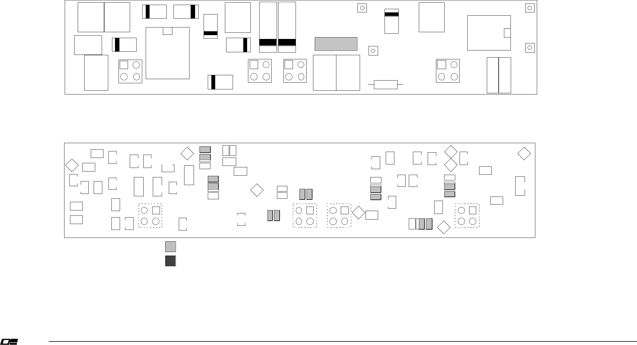
ELECTRONICS LTD.
DANIELS TM
9-14 Audio Processor Board Instruction Manual
9.11 AM Audio Processor Component
L
ayout
VICTORIA B.C .
DANIELS
ELECTRONICS
DRAWN BY: SHANE A
DWG REV DATE: AUGUST 24/98
DATE: 24 AUGUST 1998
DWG No: XXXXXAT1
DELECTRONICS
PCB 50049-04
TITLE:TX AM AUDIO PROCESSOR OUTLINE
VICTORIA B.C .
DANIELS
ELECTRONICS
DRAWN BY: SHANE A
DWG REV DATE: AUGUST 24/98
DATE: 24 AUGUST 1998
DWG No: XXXXXAT1
DELECTRONICS
TITLE:TX AM AUDIO PROCESSOR OUTLINE (bottom)
DWG No: VAP130AS1C
TITLE: TX AM AUDIO PROCESSOR LAYOUT
- COMPONENTS NOT INSTALLED
- JUMPERS INSTALLED
DWG REV DATE:AUGUST 25/98
FB 1
C1
4.7nF
R2
20k0
R5
30K9
R6
100k0
C13
1.0nF
R4
50k0
Automatic
Modulation
Control Input
Adjust
R1
5k0
Microphone
Input Level
Adjust
U1
SA571D
C3
680nF
C21
4.7uF
C12
4.7uF
C8
680nF
C9
4.7uF
R26
3M3
C6
100nF
R27
681R0
R16
5k0
Balanced
Input Level
Adjust
R17
10k0
R10
27K4
R11
27K4
C11
2.2uF
R13
18k2
R14
100k0
Modualtion
Control Output
Adjust
R22
3K48
R25
82k5
R9
10k0
U2
MC33174
C23
220pF
C19
1.0uF
R18
470k0
DWG No: VAP130AS2C
TITLE: TX AM AUDIO PROCESSOR SURFACE MOUNT DESIGNATIONS
C7
10nF
JU1
JU8
JU4
X
Y
JU7
DWG REV DATE: MARCH 06 /98
X
Y
JU3
Y
X
JU6
X
Y
JU5
X
Y
C22
680pF
R28
82k5
JU2
C20
220pF
C25
150pF
C17
330pF
R23
51k1
R32
51k1 R31
15k4
R24
15k4
R30
47k5
R20
39k2
R29
5k11
R19
5k11
C18
220pF
R15
49k9
R3
49k9 C14
100nF
JU9
R8
4k75
1
2
3
4
1
2
3
4
1
2
3
4
1
2
3
4
DWG No: VAP130AT1A
TITLE: AM TRANSMITTER THROUGH HOLE LAYOUT
D1
1N5221B
D2
1N5221B
C10
470nF
C5
470nF
C2
470nF
P 3P 2P 5P 1
DWG No: VAP130AT2B
TITLE: AM TRANSMITTER THROUGH HOLE DESIGNATIONS
C15
4.7nF C16
2.2nF
R7
1k2 TEMP
DWG REV DATE: OCTOBER / 98
wo # xxxx
TP 6
TP 8
TP 5
TP 4
TP 3
TP2
P 3
P 2 P 5
TP7
P 1
1
2
3
4
1
2
3
4
1
2
3
4
1
2
3
4
P5
P7
P8
P6
Solder Side
Component Side
MT3AMTXM8C
TP1
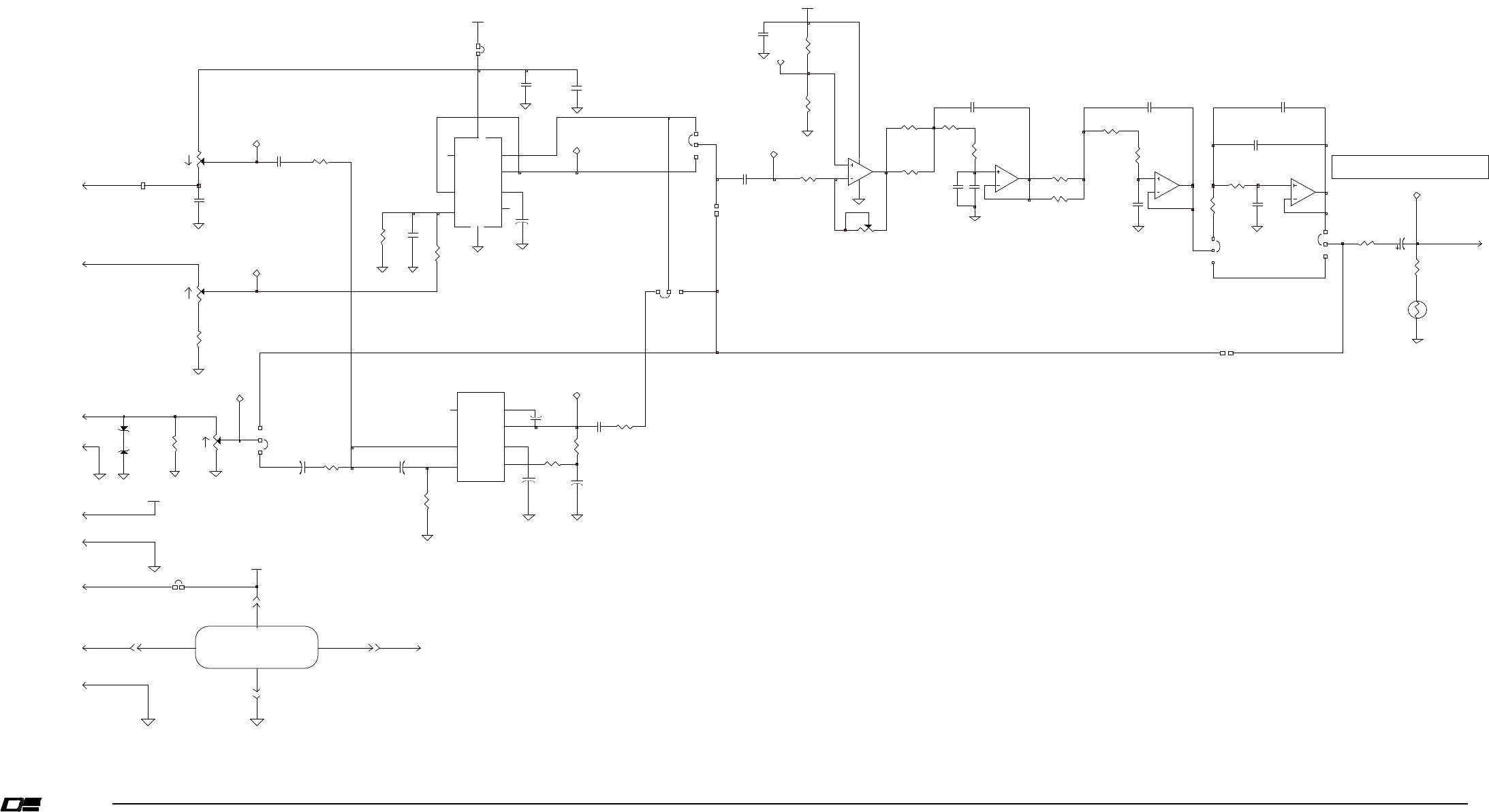
ELECTRONICS LTD.
DANIELS TM
Audio Processor Board Instruction Manual 9-15
9.12 AM Audio Processor
S
chematic Diagram
Mi
c
r
ophone Input
Le
v
e
l
Ad
j
u
s
t
Mic
r
ophone
A
utomat
i
c Modulat
i
on
s
Co nt
r
ol Input
A
dju
s
t
Balan
c
ed Input
Level Adju
s
t
Modulation
C
o ntro
l
O
utput Adju
s
t
AM C B ypass
Mod o utput
B
a
l
an
c
ed Input
9.5 Vdc
13.8 Vdc
Automati
c
Modulation C
o
ntro
l
OPTIONAL
A
ut
o
m
a
t
i
c L
e
v
e
l
C
o
n tr
o
l
X
Y
X
Y
X
Y
X
Y
X
Y
3
.
0
K
HZ
B
E
SSE
L LOW
P
A
SS
F
I
LT
E
R
3
.
0 KHZ
B
U
TTERWORTH
LOW
P
A
SS
FIILTER
App rox. 200m
V
r
m
s
@ 90% mod.
A LC B y pass
FB1
4.7nF
C1
CW 5K0
R1
TP1
470nF
C2
CW
50K0
R4
TP2
Vcc
Rect In
Var G
Rect Cap
Output
Inv In
R3
THD
Trim
GND
2
3
1
7
5
6
8
13
4
SA571D
U1a
Rect In
Var G
Rect Cap
Output
Inv In
R3
THD
Trim
15
14
16
10
12
11
9
SA571D
U1b
100K0
R6
TP3
680nF
C3
100nF
C6
10nF
C7
TP4
C8
680nF
C9
4.7uF
C10
470nF R13
18K2
CW
5K0
R16
4.7uF
C12
1.0nF
C13
R18
470K0
TP5
TP6
4.7uF
C21
TP8
MT-3 TX TIME-OUT-TIMER
3
P1
2
P5
1
P1
2
P1
3
P2
4
P1
4
P3
4
P5
4
P2
1
P3
8.0V
9.5V
8.0V
P7
-1
P8 -1
P9
-1
P6
-1
J7
-1
J8-1J6
-1
J5
-1
1N5221B
D1
1N5221B
D2
681R0
R27
2.2uF
C11
TP7
30K9
R5
2
P3
2
34
1
11
U2
MC33174
a
6
57
U2
MC33174
b
9
10 8
U2
MC33174
c
8.0V
R3
49K9
R15
49K9
C14
100nF
C16
2.2nF
13
12 14
d
MC33174
U2
100K0
R14
470nF
C5
R17
10K0
C15
4.7nF
R32
51K1
C18
220pF
R29
5K11
R19
5K11
R24
15K4
R31
15K4
R23
51K1
R28
82K5
C22
680pF
C23
220pF
JU5
R25
82K5JU7
JU8
39K2
R20
47K5
R30
330pF
C17
150pF
C25
20K0
R2
220pF
C20
JU6
3K48
R22
JU4
1.0uF
C19
10K0
R9
27K4
R10
27K4
R11
3M30
R26
JU3
JU9
4K75
R8
1K2
R7
JU2
JU1

ELECTRONICS LTD.
DANIELS TM
9-16 Audio Processor Board Instruction Manual
This Page Intentionally Left Blank

Audio Processor Board Instruction Manual 10-1
10 R
E
V
I
S
I
ON
H
I
STOR
Y
ISSUE DATE REVISION
1 Oct 2000 First Issue.
2 Nov 2000 Second Issue
Incorporated the AM Audio Processor documentation into this manual.
For specific AM revision history, see manual IM22-MT3AMTXMN-4IM

10-2 Audio Processor Board Instruction Manual
This Page Intentionally Left Blank
DANIELS
ELECTRONICS
LTD.
®
MT-3
RADIO
SYSTEMS
VHF AMPLIFIER
INSTRUCTION MANUAL
VT-3
132 - 174 MHz
Covers models:
VT-3/150 Amplifier
Copyright © 1998 Daniels
Electronics
Ltd.
All
rights
reserved.
No part of this
publication
may be
reproduced,
stored in a
retrieval
system or
transmitted
in any form or by any
means,
electronic,
mechanical,
photocopying,
recording or
otherwise,
without
the prior
written
consent of Daniels
Electronics
Ltd.
Issue: 1 Previous Issue: N/A
Issue Date: May 1998 Previous Issue Date: N/A Daniels
Electronics
Ltd.
Printing Date: January 2001
Victoria,
B.C.
Part No.: IM21-VT3150AMP PRINTED IN
CANADA

ii
VHF Amplifier Instruction Manual VT-3 132 - 174 MHz
NOTE:
The user's
authority
to op
erate
this
equipment
could be
revoked
through any
changes or
modifications
not expressly
approved
by Daniels
Electronics
Ltd.
The design of this
equipment
is subject to change due to continuous
development.
This
equipment
may
incorporate
minor changes in
detail
from the
information
contained
in this
manual.

VHF Amplifier Instruction Manual VT-3 132 - 174 MHz
iii
TABLE OF CONTENTS
Page
1 GENERAL....................................................................................................................1-1
1.1
Introduction
.......................................................................................................1-1
1.2
Performance
Specification
.................................................................................1-1
2 THEORY OF OPERATION.........................................................................................2-1
2.1
Amplifier
Operation...........................................................................................2-1
2.2 Power
Requirements
..........................................................................................2-1
2.3 RF
Circuitry
.......................................................................................................2-2
2.3.1
VT-3/150
Lowpass
Filter
.......................................................................2-2
2.4 Power Control
Circuitry
.....................................................................................2-2
2.5 Power Sensing
Circuitry
....................................................................................2-3
2.5.1 Output Power Sense ..............................................................................2-3
2.5.2 VSWR Sense.........................................................................................2-3
2.5.3 VSWR
Overload
....................................................................................2-4
3
VT-3/150 AMPLIFIER ALIGNMENT
.........................................................................3-1
3.1 General..............................................................................................................3-1
3.2 Repair Note........................................................................................................3-1
3.3
Recommended
Test
Equipment
List...................................................................3-1
3.4 Printed
Circuitboard
Numbering
Convention
.....................................................3-2
3.5 Standard Factory Settings and Jumper
Configuration
........................................3-2
3.6
VT-3/150
Amplifier
Alignment
..........................................................................3-2
3.6.1 General..................................................................................................3-2
3.6.2
VT-3/150
Amplifier
Adjustment
............................................................3-3
3.6.2.1 General Set-Up..........................................................................3-3
3.6.2.2 Output Power
Alarm
(Forward Power)......................................3-4
3.6.2.3 Output Power.............................................................................3-5
3.6.2.4
Antenna
VSWR
Alarm
(Reverse
Power)...................................3-5
3.6.2.5
Antenna
VSWR
Overload
..........................................................3-6
3.6.2.6 Procedure
Verification
...............................................................3-6
4 ILLUSTRATIONS AND SCHEMATIC DIAGRAMS................................................4-1
4.1
VT-3/150
VHF
Amplifier
Component
Layout...................................................4-2
4.2
VT-3/150
VHF
Amplifier
Schematic
Diagram...................................................4-3
4.3
VT-3/150
VHF Lowpass
Filter
Component
Layout...........................................4-5
4.4
VT-3/150
VHF Lowpass
Filter
Schematic
Diagram..........................................4-5

iv
VHF Amplifier Instruction Manual VT-3 132 - 174 MHz
5 PARTS LISTS...............................................................................................................5-1
5.1
VT-3/150
Amplifier
Electrical
Parts List............................................................5-1
5.2
VT-3/150
Low Pass
Filter
Electrical
Parts List..................................................5-3
5.3
VT-3/150
Amplifier
Mechanical
Parts List........................................................5-3
6 REVISION HISTORY..................................................................................................6-1

RF Exposure Warning
RF Exposure Warning
This transmitting equipment conforms to SAR (Specific Absorption Rate) limits regarding exposure of human
beings to radio frequency electromagnetic energy, as defined in the following national and international standards
and guidelines:
1. Industry Canada Radio Standards Specification 102 (RSS-102), Evaluation Procedure for Mobile and
Portable Radio Transmitters with respect to Health Canada’s Safety Code 6 for Exposure of Humans to
Radio Frequency Fields;
2. Health Canada Safety Code 6, Limits of Human Exposure to Radiofrequency Electromagnetic Fields in the
Frequency Range from 3 kHz to 300 GHz1;
3. United States Federal Communications Commission, Code of Federal Regulations; 47 CFR Part 1,
§ 1.1310 Radiofrequency radiation exposure limits; and
4. American National Standards Institute (ANSI) criteria for localized SAR in Section 4.2 of “IEEE Standard
for Safety Levels with Respect to Human Exposure to Radio Frequency Electromagnetic Fields, 3 kHz to
300 GHz”2.
Notes: A. The SAR limit for uncontrolled exposure of persons not classed as RF and microwave exposed
workers (including the general public) for transmitter equipment operating below 10 GHz, as defined
in the references above, is 2 W/m2 (0.2 mW/cm2).
B. This transmitting equipment is designed for use with an outdoor antenna with a characteristic antenna
gain of 10 dBi, typically mounted at a significant height above ground to provide for adequate signal
coverage. To ensure that the general public is not exposed to a power density above the recommended
limit of 2 W/m2 (0.2 mW/cm2), the equipment must be installed such that the following minimum safe
distances from the antenna are maintained:
6.3 m (20.7 ft) when configured with 100 W PA
3.5 m (11.3 ft) when configured with 30 W PA
1.8 m (5.9 ft) standalone (i.e. no PA) 8 W
C. The following power density formula has been utilized in determining minimum safe distances:
2
4
R
P
G
S
π
=
where: S = Power density (in appropriate units, e.g. mW/cm2)
P = Power input to the Antenna (in appropriate units, e.g., mW)
G = Power gain of the antenna in the direction of interest relative to an isotropic radiator
R = Distance to the center of radiation of the antenna (appropriate units, e.g., cm)
1 Minister of Public Works and Government Services, Canada 1999, Cat. H46- 2/ 99- 237E, ISBN 0- 662- 28032- 6
2 ANSI/IEEE C95.1–1992, Copyright 1992 by the Institute of Electrical and Electronics Engineers, Inc., New York, New York 10017

This Page Intentionally Left Blank

VHF Amplifier Instruction Manual VT-3 132 - 174 MHz
1-1
1
GENERAL
1.1 Introduction
The
VT-3/150
Amplifier
provides
the final stage of RF
amplification
and
filt
ering for the
entire
VHF
Transmitter
VT-3 132 - 174 MHz
family.
The
amplifier
has two
distinct
frequency ranges:
132 to 150 MHz, and 150 to 174 MHz
with
continuously
adjustable
2.0 to 8.0 Watts output power.
The
VT-3/150
Amplifier
is housed in a
machine
d
aluminum
case that ensures
optimum
RF
shielding,
provides
a good ground, and also acts as a heatsink.
Additionally,
the
VT-3/150
Amplifier
is equipped
with
output power and VSWR sensing lines
which
can be
individually
configured as open
collector
or linear outputs. The
internal
VSWR
sensor protects the
amplifier
from high
antenna
VSWR by
approximately
halving
the
amplifier's
RF gain when a VSWR
overload
condition
is present.
Output
filtering
for the
VT-3/150
Amplifier
is
provided
by the
VT-3/150
Lowpass
Filter
Board.
The lowpass
filter
assembly is mounted in a
separate
compartment
of the
amplifier
case in order to
provided
maximum
attenuation
of
harmonic
and other spurious signals.
Refer to Section 4 for the VT-3 132 - 174 MHz VHF
amplifier
and lowpass
filter
component
layouts and
schematic
diagrams
1.2
Performance Specification
Type: MT-3 series VHF
Amplifier
module.
Compatibility:
MT-3 series
Transmitter
Main Board.
Frequency Range: 132 MHz to 150 MHz or 150 MHz to 174 MHz.
RF Power Output:
adjustable
2.0 to 8.0 Watts
RF power Input:
nominal
level
adjustable
from
+4
dBm to
+10
dBm,
held
within
+/- 2 dB of
nominal.
Ouput
Impedance
and VSWR: 50 Ω, Type N
connector;
3:1 max. VSWR.
Input /Output
Isolation:
> 60 dB
Duty
Cycle:
100%: Continuous
operation
from -40˚ C to +60˚C.
Harmonic Emissions: Less than -80 dBc .

1-2
VHF Amplifier Instruction Manual VT-3 132 - 174 MHz
Transmitter
Mismatch
Protection:
20:1 VSWR at all phase angles.
Transmitter
Alarm:
Forward power sense and
reverse
VSWR;
- open
collector
output
(separate
or 'OR'ed
configuration);
-linear
output
(separate
lines only).
Operating
Temperature
Range: -30˚ C to +60˚
C,
optional
-40˚ C te
mperature
test.
Operating
Humidity:
95% RH (non-condensing) at +25˚ C.
Operating
Voltage:
+13.8
Vdc Nominal (range
+11
to
+16
Vdc),
+9.5
Vdc
Regulated.
Transmit
Current: 0.7 Amp
typical;
1.1 Amp
maximum
Amplifier
Standby Current: less than 0.5 mA.
Amplifier
Enable:
Active
to ground.
Amplifier
Enable
Response:
typically
overdamped,
rising to
within
90% of full power
within
5 msec;
maximum
(underdamped)
overshoot
of 30%.

VHF Amplifier Instruction Manual VT-3 132 - 174 MHz
2-1
2
THEORY OF OPERATION
2.1
Amplifier Operation
A power control
circuit
monitors the RF output power of
amplifier
U4 and keeps the power
constant. The output power from the high power
amplifier
will
change as the
unregulated
+13.8
Vdc supply
varies.
Note that the frequency band does not change how the
amplifier
operates;
it only
changes a few
component
values
in the RF
circuitry.
Power for the
VT-3/150
Amplifier
is
provided
from the MT-3
Transmitter
Board. The
+13.8
Vdc
supply (if required) is
continuously
connected
to the
amplifier;
whereas,
the
+9.5
Vdc supply is
always switched
by the
transmitter's
PTT
circuitry.
The
VT-3/150
Amplifier
will
not use any power
from the
+13.8
Vdc supply
until
the
amplifier's
+9.5
Vdc line is
switched
on and an RF input
signal is present. The synthesizer or crystal control module controls the
+9.5
Vdc to the
amplifier's
circuitry;
switching
it on by grounding the
amplifier's
input
enable
line. The synthesizer or crystal
control module
will
ground the input
enable
line only when the RF signal from the synthesizer or
crystal control module is phase locked. This
prevents
unwanted
spurious emissions during
transmitter
start-up. A
typical
start-up sequence is shown
below:
1) the
transmitter
is keyed on
(+13.8
Vdc is
always
present)
2)
+9.5
Vdc is
switched
on by the PTT
circuitr
y and the synthesizer
or crystal control module PTT line is pulled low
3) an RF signal is output to the
amplifier
4) the
amplifier's
input
enable
line is
activated
5) the
amplifier
outputs RF power
2.2
Power Requirements
Typical
current
requirement
s for the
VT-3/150
Amplifier
at
different
power
levels
are
given
in the
Table
2-3
below.
The current drawn from the
+9.5
Vdc supply should
never
exceed
1.2 Amps and
the current drawn from the
+13.8
Vdc supply should
never
exceed
1.5 Amps.
Table 2-1
VT-3/
150 Amplifier Current Consumption
Output
Power
+9.5 Vdc
Supply Current
+13.8 Vdc
Supply Current
2.0 W 0.64 A 0.51 A
4.0 W 0.79 A 0.75 A
6.0 W 0.89 A 0.93 A
8.0 W 1.04 A 1.10 A
Note: Current consumption measured at 153 MHz

2-2
VHF Amplifi
er Instruction Manual VT-3 132 - 174 MHz
2.3 RF Circuitry
The RF c
ircuitry
consists of
several
blocks: a 7 dB input pad (R1,
R2,
and R3), an RF
amplifier
module (U4), an output power boosting transistor (Q7), three
directional
couplers
(TL1,
TL3,
and
TL4),
and the
VT-3/150
Lowpass
Filter.
The heart of the
VT-3/150
Ampl
ifier is RF
amplifier
module U4. The output of U4 is further
amplified
by Q1 to a
maximum
of 8.0 Watts at the
antenna
connector.
The frequency band of the
VT-3/150
Amplifier
is
determined
by the
operating
frequency
range of the RF
amplifier
module U4. D
irectional
couplers
(TL1,
TL3,
and TL4) are used to sample
forward and
reverse
power. The sampled power is used by the sensing and power control
circuits
to
control the
amplifier's
operation.
The final step in the RF path is output
filtering
and,
as
ment
ioned
earlier,
this is done by the
VT-3/150
Lowpass
Filter.
2.3.1
VT-3/150 Lowpass Filter
The
VT-3/150
Lowpass
Filter
is a 50
ohm,
9
pole,
reciprocal
filter
with
a 3 dB cutoff frequency of
approximately
185 MHz. The lowpass
filter
assembly
attenuates
the desired signal's harmonics as
well
as any other out-of-band emissions so that a
'clean'
RF signal is output to the
antenna
connector.
2.4
Power Control Circuitry
The
VT-3/150
Amplifier
employs a closed loop power control
which
uses a sample of the forward
RF power to control the gain of RF
amplifier
U4. Op-amp U1b compares the sampled RF
voltage
to the output power
setpoint
and
generates
an error signal
which
Q3 uses to control the
voltage
on
U4's gain control pin. The output power
setpoint
is determined by
R7,
the Output Power
Adjust
potentiometer.
The forward power is sampled by
TL1,
D5,
C14, R13,
L6,
R12,
and C15. The power control
circuitry
keeps the output power of U4 constant.
Therefore
the
amplifier's
output power
will
fluctuate
with
variat
ions in the
+13.8
Vdc supply
voltage.

VHF Amplifier Instruction Manual VT-3 132 - 174 MHz
2-3
2.5
Power Sensing Circuitry
The
VT-3/150
Amplifier
is equipped
with
output power and VSWR sensing lines
which
can be
individually
configured as open
collector
or
linear
outputs. In open
collector
configuration,
the
output is
active
low,
that
is,
when a fail
condition
is
detected
(not enough output power or too high
antenna
VSWR) the open
collector
transistor is turned on. In
linear
configuration,
a
voltage
proportional
to the sensed output power or
antenna
VSWR is output.
Both the Output Power
Alarm
setpoint
and the VSWR
Alarm
setpoint
are
individually
adjustable;
however,
the Output Power
Alarm
setpoint
must
always
be adjusted before the VSWR
Alarm
setpoint.
This is because the Output Power
Alarm
setpoint
is used as a
reference
by the VSWR
Alarm
circuitry.
2.5.1
Output Power Sense
The output power sense
circuitry
uses
directional
coupler TL2 to sample some of the forward
power. The sampled power is
rectified
by diode D6 and
capacitor
C20 and then
amplified
by
op-amp U3b. Op-amp U3b's
amplification
is
controlled
by
R21,
the output power
alarm
adjust
potentiometer.
The
amplified
voltage
is then output
directly
in
linear
operation
(JU1
installed,
JU2
not
installed)
or
compared
by op-amp U1a
which
then
drives
transistors Q4 and Q3 for open
collector
operation
(JU1 not
installed,
JU2
installed).
In open
collector
configuration,
Q3 (the open
collector
output transistor) is turned on when an
alarm
condition
occurs. The
adjustment
range for the output power
alarm
can
vary
depending on
the
setting
of R21 (the Output Power
Alarm
Adjust
potentiometer).
2.5.2
VSWR Sense
The VSWR sense
circuitry
uses
directional
coupler TL3 to sample some of the power
reflected
from the
antenna
terminal.
The
reflected
power is
rectif
ied by diode D7 and
capacitor
C25 and then
amplified
by op-amp U2b. Op-amp U2b's
amplification
is
controlled
by
R36,
the VSWR
Alarm
Adjust
potentiometer.
The
amplified
voltage
is then output
directly
in
linear
operation
(JU4
installed,
JU3 not
installed)
or
compared
to the output power
alarm
setpoint
by op-amp U3a
which
then
drives
transistor Q5 for open
collector
operation
(JU4 not
installed,
JU3
installed).
In open
collector
configuration,
Q5 (the open
collector
output transistor) is turned on when an
alarm
condition
occurs. The
adjustment
range for the VSWR
Alarm
can depending on the
setting
of R36 (the VSWR
Alarm
Adjust
potentiometer).

2-4
VHF Amplifi
er Instruction Manual VT-3 132 - 174 MHz
2.5.3 VSWR Overload
The VSWR
overload
circuit
protects the
VT-3/150
Amplifier
from
excessive
antenna
VSWR by
reducing the
amplifier's
gain (output power) when an
overload
condition
occurs. The VSWR
overload
circuit
(R14,
R37, R39, R40,
U2a, and Q6) is an extension of the VSWR sense
circuit
and
operates the same as the VSWR sense open
collector
circuit.
The VSWR Overload
Adjust
potentiometer
(R37) reduces the
voltage
level
of the VSWR
Alarm
Setpoint.
The
voltage
set by
R37 is the
compared
to the output power
alarm
setpoint
by op-amp U2a
which
then
drives
transistor Q6. When transistor Q6 turns on,
signaling
an
over
load
condition,
resistor R14 is
grounded
which
reduces the output power
setpoint.
Reducing the output power
setpoint
lowers the
VT-3/150
Amplifier's
gain and protects the
amplifiers
from
excessive
current draw resulting from
high
antenna
VSWR.
The VSWR overload
circuit's
range of
adjustment
depends on the
setting
of the VSWR
Alarm
Adjust
potentiometer
(R36). The VSWR
overload
transistor Q6 can be
activated
at the same point
at
which
the VSWR
alarm
becomes
active
or the VSWR
overload
circuit
can be disabled by turning
R37
completely
counterclockwise.

VHF Amplifier Instruction Manual VT-3 132 - 174 MHz
3-1
3
VT-3/150 AMPLIFIER ALIGNMENT
3.1
General
Connections to the power
supply,
alarm
and
transmit
enable
lines
(ENA),
are
clearly
marked on the
amplifier
case. The
amplifier
is
enabled
when the
enable
line (ENA) is grounded.
If the
amplifier
is
installed
in the
transmitter,
alignment
is
simplified
by using an SR-3
Subrack,
SM-3 System
Monitor,
and RF
extender
cable
to
provide
transmitter
power and signal
interconnection
(see the
Transmitter
Main Board Manual for
details).
For
complete
transmitter
alignment,
the
Transmitter
Main
Board,
Synthesizer,
Amplifier,
and Audio Processor should be
tuned in the
aforementioned
order. Please refer the corresponding manuals for each module.
If the input RF
level
is not chan
ged,
adjustments
to the output power and
alarm
thresholds may be
made
without
removing
the
amplifier
cover.
However,
in the case of a
complete amplifier
alignment,
the
amplifier
should be
separated
from the
Transmitter
Main Board and the
amplifier
cover
re
moved
to expose all
amplifier
circuitry.
All
jumpers and test points are
clearly
marked.
3.2 Repair Note
The
VT-3/150
Amplifier
is
mainly
made up of surface mount
devices
which
should not be
removed
or
replaced
using an ordinary soldering iron.
Removal
and
replacement
of surface mount
components should be performed only
with
specifically
designed surface mount rework and repair
stations
complete
with
ElectroStatic
Dissipative
(ESD)
protection.
When
removing
Surface Mount Solder Jumpers, it is
recommende
d to use solder braid in
place
of
manual
vacuum
type desoldering tools when
removing
jumpers. This
will
help
prevent
damage
to
the
circuitboards.
3.3 Recommended Test Equipment List
Alignment
of the
transmitter
requires the
following
test
equipment
or its
equivalent.
Dual Power Supply:
Regulated
+9.5
Vdc at 0.1 A.
Regulated
+13.8
Vdc at 2 A -
Topward
TPS-4000
Oscilloscope /
Multimeter:
Fluke 97
Scopemeter
Current Meter: Fluke 75
multimeter
Radio
communications
test set : Marconi Instruments 2955R
VSWR 3:1
mismatch
load:
JFW
50T-035-3.0:1
coaxial
test
cable
set three 50 Ω cables of
incremental
length 20 to 40 cm
Alignment
Tool:
Johanson 4192

3-2
VHF Amplifier Instruction Manual VT-3 132 - 174 MHz
It is
recommended
that the radio
communications
test set be frequency locked to an external
reference
(WWVH, GPS, Loran C) so that the high
stability
oscillator
may be
accurately
set to
within
its
±1
ppm frequency
tolerance.
3.4
Printed Circuitboard Numbering Convention
To ease
troubleshooting
and
maintenance
procedures,
Daniels
Electronics
Limited
has adopted a
printed
circuitboard
(PCB) numbering
convention
in
which
the last two digits of the
circuitboard
number represent the
circuitboard
version.
For
example:
• PCB number 43-912010
indicates
circuitboard
version
1.0;
• PCB number 50002-02
indicates
circuitboard
version
2.0.
All
PCB's
manufactured
by Daniels
Electronics
are
identified
by one of the
above
conventions.
3.5
Standard Factory Settings and Jumper Configuration
The
VT-3/150
Amplifier
is factory configured as
follows:
• Open
collector
configuration
for Output Power
Alarm.
• Open
collector
configuration
for
Antenna
VSWR
Alarm.
The corresponding jumper settings are:
• Jumper JU1: not
installed
Output power
alarm
-
linear
output
• Jumper JU2:
installed
Output power
alarm
- open
collector
output
• Jumper JU3:
installed
Antenna
VSWR
alarm
- open
collector
output
• Jumper JU4: not
installed
Antenna
VSWR
alarm
-
linear
output
3.6 VT-3/150 Amplifier
Alignment
invisible
text
3.6.1 G
eneral
The
VT-3/150
Amplifier
is a frequency
sensitive
module that is factory assembled to
operate
in one
of two frequency bands: 132 to 150 MHz or 150 to 174 MHz. The
amplifier
requires 7 dBm of
input power and is
continuously
adjustable
over
the its power range of 2.0 to 8.0 Watts. The
VT-3/150
Amplifier
provides
Output Power and
Antenna
VSWR
Alarm
outputs
which
can be
configured for open
collector
output or
linear
operation.
The
amplifier's
output power
level
and
alarm
levels
can be set
without
detaching
the
amplifier
from the
transmitter
board.
However,
to
change the
configuration
of the output power
alarm
or the
Antenna
VSWR
alarm,
the VT-3/150
Amplifier
must be
detached
from the MT-3
Transmitter
Board. Refer to page 4-2
"VT-3/150
VHF
Amplifier
Component
Layout" for the
location
of solder jumpers JU1 to JU4.

VHF Amplifier Instruction Manual VT-3 132 - 174 MHz
3-3
3.6.2
VT-3/150 A
mplifier
Adjustment
The
Amplifier
alignment
consists of two
adjustment
procedures; (i) a
general
set up (section
3.6.2.1) procedure
which
sets up the proper bias
conditions
for the RF transistors and (ii) the RF
threshold
adjustments
which
set up the desired
alarm
threshold
levels
as
well
as the RF output
power. The
general
alignment
procedure is required
following
major repair
operations,
changes in
RF input
levels
or large changes in
operating
frequency
(greater
than
±
1.0 MHz).
The RF output and
alarm
threshold
level
adjustments
are more easily
accessible
so that fine
adjustments
can be made in the field. Depending on user
requirements,
the RF
alarm
threshold
levels
should be
checked
whenever
a
significant
change in
operating
frequency
(±
0.5 MHz) is
made. As the
antenna
VSWR
alarm
is
dependent
on the output power
alarm,
the output power
alarm
should
always
be set first. The order of
adjustment
should be:
1) Set the desired output power
alarm
level
(section 3.6.2.2).
2) Set the output power (section 3.6.2.3).
3) Set the desired
Antenna
VSWR
alarm
level
(section 3.6.2.4).
4) Set the desired
overload
condition
level
(section 3.6.2.5).
Details for the
alignment
steps are
outlined
below.
3.6.2.1
General S
et-Up
All
of the setup steps
detailed
below
are performed at the factory as part of the
initial
Transmitter
alignment.
A
general
realignment
of the
Amplifier
Module
will
be required
under the
following
conditions:
(i) the
nominal
RF input power
applied
to the
amplifier
is changed from that
which
the
amplifier
was
intially
set up for, and
(ii)
components,
particularly
the RF transistors Q1 and Q2, are
replaced
during a repair
operation.
1. Connect the
transmitter's
antenna
output
connector
to the type N input of the radio
communications
test set through a short section of low loss 50 Ω
coaxial
cable.
2. Turn all four (4) of the
adjustment
potentiometers
(R7,
R21, R36,
and R37) fully
counterclockwise.
3. Turn on the power to the
transmitter.

3-4
VHF Amplifier Instruction Manual VT-3 132 - 174 MHz
4. Monitor the
+9.5
Vdc and 13.8 Vdc supply current and adjust
R7,
the output power
adjustment,
so that
approximately
1 Amp is being drawn on the
+9.5
Vdc line and 1.3
Amps or less is being drawn on the 13.8 Vdc line. This should produce
approximately
8 Watts.
5. If only a 6 or 7
watt
output is
obtained,
adjust the low pass
filter
coil pairs L2/L3 and
L1/L4 to obtain 8
watts.
3.6.2.2
Output Power Alarm (Forward Power)
Open
Collector
Output
*
note:
the output power
alarm
output is factory configured as an open
collector
output
so a pull-up resistor may be required on
transmitter
pin B26 if one is not
already
present.
1.
Adjust
R7,
the output power
adjustment,
to the output power at
which
the Output
Power
Alarm
is to be
activated.
2. Monitor
transmitter
pin
B26,
the Output Power
Alarm
line,
and
slowly
turn
R21,
the
output power
alarm
adjustment,
clockwise
until
pin B26 goes low. The
alarm
is now
set for the current output power of the
transmitter.
Linear
Output
1. Open the
amplifier
case to disable (open
circuit)
jumper JU2 and
enable
(short)
jumper JU1.
2. Monitor
transmitter
pin B26
with
a
voltmeter.
3.
Adjust
R7,
the output power
adjustment,
for full
transmitter
output power.
4.
Adjust
R21,
the output power
alarm
adjustment,
so that the
voltmeter
ind
icates
+7.5
Vdc for full
transmitter
output power.
5. Turn
R7,
the output power
adjustment,
fully
counterclockwise.
The
voltmeter
should
read
approximately
+3
Vdc.
6. Disconnect the
voltmeter.

VHF Amplifier Instruction Manual VT-3 132 - 174 MHz
3-5
3.6.2.3 Output Power
1. Turn
R7,
the output power
adjustm
ent,
clockwise
to the desired
transmitter
output
power.
3.6.2.4 Antenna VSWR Alarm (Reverse Power)
Open
Collector
Output
*
note:
the
antenna
VSWR
alarm
output is factory configured as an open
collector
output so a pull-up resistor may be required on
transmitter
pin Z26 if one is not
already
present. The output power
alarm
must be set first before the
antenna
VSWR
alarm
can be set.
1. Disconnect the radio
communications
test and
terminate
the
transmitter
with
the 3:1
mismatch
load.
2. Monitor pin
Z26,
the
Antenna
VSWR
Alarm
line,
and turn R36 fully
counterclockwise.
Pin Z26 should be high.
Slowly
turn R36
clockwise
until
pin Z26
is pulled low. Put the 50 ohm load back on
again,
Pin Z26 should go high. The
reverse
power trip point is now set for a VSWR of 3:1.
Linear
Output
1. Open the
amplifier
case to disable (open
circuit)
jumper JU3 and
enable
(short)
jumper JU4.
2. Monitor
transmitter
pin Z26
with
a
voltmeter.
3. Disconnect the radio
communications
test set and
terminate
the
transmitter
with
the
3:1
mismatch
load.
4.
Adjust
R36,
the VSWR
alarm
adjustment,
so that the
voltmeter
indicates
+5
Vdc for a
3:1
mismatch.
5. Put the 50 ohm load back on again. The
voltmeter
should read
approximately
0 Vdc.
6. Disconnect the
voltmeter.

3-6
VHF Amplifier Instruction Manual VT-3 132 - 174 MHz
3.6.2.5 Antenna VSWR Overload
1. Disconnect the radio
communications
test set and so that the
amplifier
is
terminated
with
an open
circuit.
2. Monitor the current from the
+9.5
Vdc supply.
3.
Adjust
R37,
the VSWR
overload
adjustment,
clockwise
until
a
noticeab
le drop in the
+9.5
Vdc current occurs.
4.
Reconnect
the radio
communications
test set
and,
the
+9.5
Vdc current should return
to the
previous
level.
3.6.2.6
Procedure Verification
1.
Verify
that the current drawn from the
+13.8
Vdc supply is less than 1.5 A and from
the
+9.5
Vdc supply is less than 1.2 A when
transmitting
full RF output power (8
Watts).
2. Turn off the power to the
transmitter.

DE
DANIELS
ELECTRONICS
4-1
VHF Amplifier Instruction Manual VT-3 132 - 174 MHz
4
ILLUSTRATIONS AND S
CHEMATIC DIAGRAMS
This Page Intentionally Left Blank
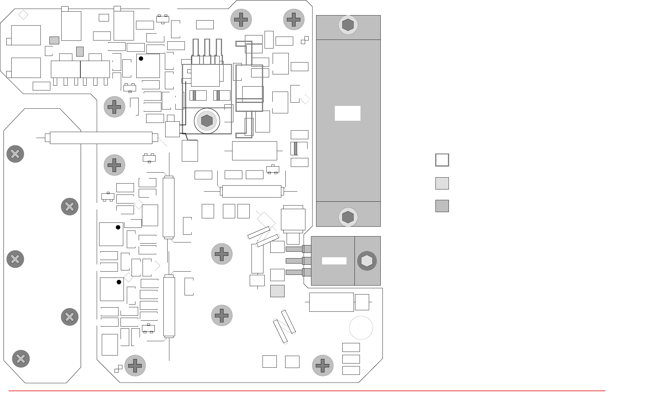
DEFAULT JUMPER
VICTORIA B.C .
DATE.:
DWG No:
TITLE:
D
DANIELS
ELECTRONICS
BOARD No.:
DWG REV DATE:
43-932611
MARCH 8, 1994
COMPONENT NOT INSTALLED
VT-3/150 AMPLIFIER SM LAYOUT (LOW POWER)
9326AS1
49R9
49R9
150p
49K9
1.5uH
49K9
10n
10n
100n
49K9
49K9
1K
10n
10K
10K
100n
10K
10n
1.5uH
33172
33172
27K4
1K
1K
49K9
10K
1K
49K9
49K9
10n
10n
10K
10nF
10K
MC
49K9
10K
10K
27K4
1K
1K
4K53
10K
27K4
100n
10n
1nF
30R1
0.18uH
0.18uH
FB1
0.18uH
1nF
100nF
18nF
18nF
18nF
18nF
4.7uF
10nF
BYD17J
100nF
49K9
MMBD701
MMBD701
BC817-25
BC817-25
MBZ5233B
PZT2222A
PZT2222A
50K
50K
50K
50K
D6
C20
R18
L6
R19
C21
C19
C18
R20
C22
R22
R23
R24
R32
R44
C24
R43
R42
R35
R34
U2
U3
R40
C26
TL2
TL3
R16
R17
D7
C25
R33
L7
R39
R41
Q6
R26
R27
R30
R11
R9
C12
C15
C17
Q4
R31
R28
R29
U1
R10
R5
C13
C14
D1
R6
R8
R7
R25
Q3
Q5
R38
R37
R36
R21
33172
R1
C1
C2
C3
C4
L1
L3
L2
C9
18nF
Q2
D5P06V
R4
D3
D4
C6
C5
MC
MC
C10
C7
C8
C11
JU1
JU2
JU3
JU4
3K48
221K
C23
10n
R14
10K
150p
49K9
VT-3/150 AMPLIFIER SM DESIGNATION (LOW POWER)
9326AS2
BYD17J
R2
R3
178R
178R
JU5
VT-3/150 AMPLIFIER SM LAYOUT (HIGH POWER)
9326AS3
100nF
10nF
SELECT
SELECT
1nF
SELECT
SELECT
49K9
49R9
150pF
49K9
1.5uH
MMBD701
SELECT
SELECT
D5
C16
R15
R13
L5
C31
C33
C29
C37
C38
R12
TL1
C27
C28
C32
C34
VT-3/150 AMPLIFIER SM DESIGNATION (HIGH POWER)
9326AS4
SELECT
C36
COMPONENT INSTALLED ON BOTTOM OF BOARD
COMPONENT MOUNTED ON CASE
M2.5 x 6 SCREW
M3 x 8 SCREW
VT-3/150 AMPLIFIER TH LAYOUT (LOW POWER)
M3 x 8 CAP SOCK SCREW
NOTE
Q1 MOUNTED ON CASE WITH LEADS
INSERTED TO BOTTOM OF BOARD
150nH
L4
TL2
TL3
TL5
TL4
Q1
IRF9540
D2
1N5402
VT-3/150
LOW PASS
FILTER ASSEMBLY
VT-3/150 AMPLIFIER TH DESIGNATION (LOW POWER)
9326A5
MHW607
SELECT
2.2nF
C39
150nH
FB3
47uF
C30
+
FB2
150nH
10R
L11
19nH
L8
L9
L10
19nH
R45
C35
SELECT
MRF262
TL1
VT-3/150 AMPLIFIER TH LAYOUT AND DESIGNATION (HIGH POWER)
9326A6
M3 x 6 CAP SOCK SCREW
4-2
4.1
VT-3/150 VHF Amplifier Component Layout
DE
DANIELS
ELECTRONICS
VHF Amplifier Instruction Manual VT-3 132 - 174 MHz
VT3AMPM1
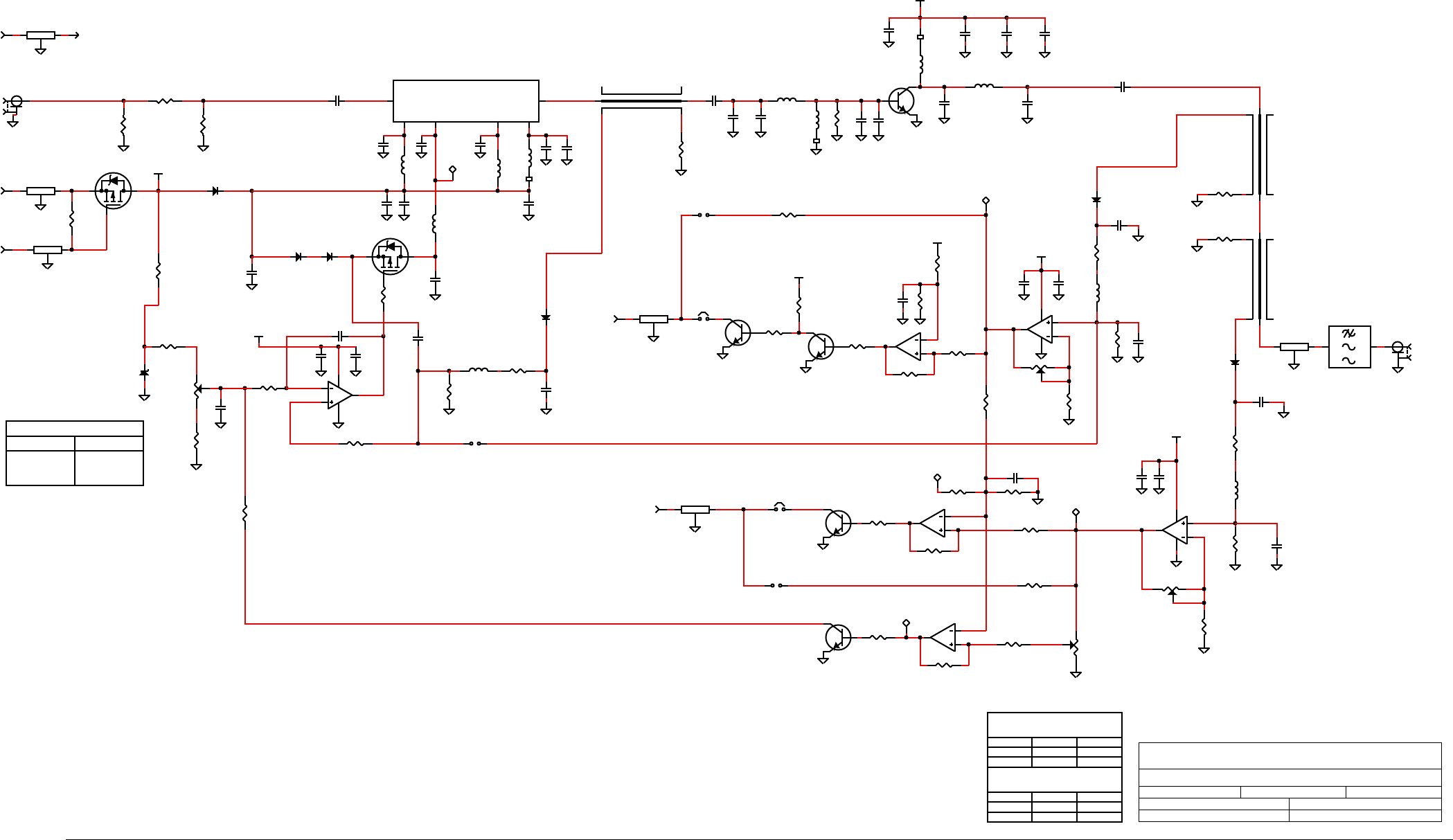
R6
POWER
27k4
2 - 8 Watts
392k
2 - 5 Watts
Power Range Selection
DE
DANIELS
ELECTRONICS
VICTORIA B.C.
DE
DANIELS
ELECTRONICS
4
.
2
V
T
-
3
/
150
V
HF
A
m
p
li
f
i
e
r
S
c
h
e
m
a
t
i
c
D
i
a
g
ra
m
TITLE: VT-3/150 VHF AMPLIFIER SCHEMATIC DIAGRAM
4-3
VHF Amplifier Instruction Manual VT-3 132 - 174 MHz
J2, JU5
DWG No: VT3AMPM2A DWG REV DATE: 10 DECEMBER 1995
DATE: 4 MARCH 1994
FORWARD
POWER
ALARM
C39
FORWARD
OUTPUT ALARM
ADJUST
VSWR
OUTPUT ALARM
ADJUST
OVERLOAD
ADJUST
OUTPUT
POWER
ADJUST
LB = LOW BAND
HB = HIGH BAND
U4
TL5, TP5
R45
Q7
L11
FB3, FIL5
D7
DWN BY: REX WONG
BOARD REV: 1.1BOARD No: 43-932611
APRVD:
-----
-----
-----
-----
-----
-----
-----
-----
-----
UNUSED REFERENCE DESIGNATORS
HIGHEST REFERENCE DESIGNATORS
VSWR
ALARM
+13.8 VDC
LOW / HIGH BAND
RF IN (1 mW)
SMB
J1
RF OUT
TYPE N JACK
J2
10k0
R9
10nF
C15
50k
R7
MBZ5233B
D1
4k53
R5
10k0
R10
10nF
C12
DS
Q2
D5P06V
TL5
178R
R3
30R1
R1
49k9
R4 IN5402
D2
LPF
FIL1
AMPLIFIER ENABLE I/P
LPF
FIL2
+9.5 VDC
LPF
FIL5*
+13.8 VDC
LPF
DS
IRF9540
Q1
3k48
R8
SEL
R6
BYD17J
D4
178R
R2
BYD17J
D3
1.5uH
L5
49k9
R13
150pF
C16
49k9
R12
TL1
R15
49R9
1k00
R35
49k9
R34
10nF
C26
PZT2222A
Q5
10k0
R44
50k
R36
150pF
C25
49k9
R33
1k00
R42
27k4
R43
10nF
C23
6
5
8
7
4
MC33172
U2b
1.5uH
L7
MMBD701
D7
10k0
R11
TL2
49R9
R16
49R9
R17
49k9
R22
10k0
R20
50k
R21
49k9
R19
10nF
C21
150pF
C20
49k9
R18
1.5uH
L6
MMBD701
D6
BC817-25
Q4
10k0
R29
1k00
R25
27k4
R28
BC817-25
Q6
10k0
R41
1k00
R39
221k
R40
49k9
R27
10nF
C17
49k9
R26
49k9
R30
PZT2222A
Q3
10k0
R31
50k
R37
1k00
R38
JU1
JU4
1k00
R24
2
3
1
U3a
2
3
1
U1a
2
3
1
U2a
6
5
8
7
4
MC33172
U3b
100nF
C18
10nF
C19
100nF
C13
10nF
C14
6
5
4
7
8
MC33172
U1b
LPF
FIL3 JU2
LPF
FIL4 JU3
100nF
C24
TL3
100nF
C11
18nF
C9
180nH
L3
18nF
C5
+
4.7uF
C6
18nF
C4
180nH
L2
180nH
L1
150nH
L4
18nF
C2
18nF
C3
MHW 607
6
MHW607
U4
FB1
1nF
C1
MRF262
Q7
+13.8 VDC
150nH
L10
150nH
L9
C31
51pF LB/24pF HB
FB2
SELECT
C35
56pF LB/220pF HB
C38
FB3*
+
47uF
C30
10nF
C28
100nF
C27
19nH
L8
19nH
L11
47pF LB/43pF HB
C36
47pF LB/36pF HB
C37
68pF LB/51pF HB
C33
10R
R45
MMBD701
D5
10k0
R32
TP3
TP4
TP5
TP2
TP1
1nF
C8
100nF
C7
10nF
C10
49k9
R23
10nF
C22
10k0
R14
20pF LB
C34
5.6pF LB
C32
1nF
C29
SWITCHED +9.5V
SWITCHED +9.5V
TO ALL SWITCHED +9.5V
SWITCHED +9.5V
SWITCHED +9.5V
SWITCHED +9.5V
2.2 nF
C39
JU5
2 4 5
1
3
OVERLOAD

DE
DANIELS
ELECTRONICS
4-4
VHF Amplifier Instruction Manual VT-3 132 - 174 MHz
This Page Intentionally Left Blank
VHF Amplifier Instruction Manual VT-3 132 - 174 MHz
4-5
4.3
VT-3/150 VHF Lowpass Filter Component Layout
invisible
text
4.4 VT-3/150 VHF Lowpass Filter Schematic Diagram

4-6
VHF Amplifier Instruction Manual VT-3 132 - 174 MHz
This Page Intentionally Left Blank

VHF Amplifier Instruction Manual VT-3 132 - 174 MHz
5-1
5
PARTS LISTS
5.1 VT-3/150
Amplifier Electrical Parts List
Ref
Desig Description Part No.
C1
CAP.,
SM,
1nF
CER,
1206, C0G
1008-3B102K1G
C2-C5
CAP.,
SM,
18nF
CER,
1206, X7R 1008-4B183K5R
C6
CAP.,
SM,
4.7µF
TANT., 10%, 16V
1055-5B475K16
C7 C
AP.,
SM,
100nF
CER,
1206, X7R 1008-5B104K5R
C8
CAP.,
SM,
1nF
CER,
1206, C0G
1008-3B102K1G
C9
CAP.,
SM,
18nF
CER,
1206, X7R 1008-4B183K5R
C10
CAP.,
SM,
10nF
CER,
1206, X7R 1008-4B103K5R
C11
CAP.,
SM,
100nF
CER,
1206, X7R 1008-5B104K5R
C12
CAP.,
SM,
10nF CER, 1206, X7R 1008-4B103K5R
C13
CAP.,
SM,
100nF
CER,
1206, X7R 1008-5B104K5R
C14,
C15
CAP.,
SM,
10nF
CER,
1206, X7R 1008-4B103K5R
C16
CAP.,
SM,
150pF
CER,
1206, C0G
1008-2B151J1G
C17
CAP.,
SM,
10nF
CER,
1206, X7R 1008-4B103K5R
C18
CAP.,
SM,
100nF
CER,
1206, X7R 1008-5B104K5R
C19
CAP.,
SM,
10nF
CER,
1206, X7R 1008-4B103K5R
C20
CAP.,
SM,
150pF
CER,
1206, C0G
1008-2B151J1G
C21-C23
CAP.,
SM,
10nF
CER,
1206, X7R 1008-4B103K5R
C24
CAP.,
SM,
100nF
CER,
1206, X7R 1008-5B104K5R
C25
CAP.,
SM,
150pF
CER,
1206, C0G 1008-2B151J1G
C26
CAP.,
SM,
10nF
CER,
1206, X7R 1008-4B103K5R
C27
CAP.,
SM,
100nF
CER,
1206, X7R 1008-5B104K5R
C28
CAP.,
SM,
10nF
CER,
1206, X7R 1008-4B103K5R
C29
CAP.,
SM,
1nF
CER,
1206, C0G
1008-3B102K1G
C30
CAP.,
47µF
DIP. TANT., 20%, 35V 1054-6M476M35
C31 C
AP.,SM,
51pF
PORCEL.,
5% 500V 1036-1B2510J5 (132 - 150 MHz)
C31
CAP.,SM,
24pF
PORCEL.,
5% 500V 1036-1B2240J5 (150 - 174 MHz)
C32
CAP.,SM,
5.6pF
PORCEL.,
±0.25pF
500V 1036-0B2569C5 (132 - 150 MHz)
C32
CAP.,SM,
NOT INSTALLED NOT INSTALLED (150 - 174 MHz)
C33
CAP.,SM,
68pF
PORCEL.,
5% 500V 1036-1B2680J5 (132 - 150 MHz)
C33
CAP.,SM,
51pF
PORCEL.,
5% 500V 1036-1B2510J5 (150 - 174 MHz)
C34
CAP.,SM,
20pF
PORCEL.,
5% 500V 1036-1B2200J5 (132 - 150 MHz)
C34
CAP.,SM,
NOT INSTALLED NOT INSTALLED (150 - 174 MHz)
C35 CAP
.,
330pF METAL CLAD,1% 250V 1046-2A331FDB (132 - 150 MHz)
C35
CAP.,
270pF METAL CLAD, 1% 250V 1046-2A27TFDB (150 - 174 MHz)
C36
CAP.,SM,
47pF
PORCEL.,
5% 500V 1036-1B2470J5 (132 - 150 MHz)
C36
CAP.,SM,
43pF
PORCEL.,
5% 500V 1036-1B2430J5 (150 - 174 MHz)
C37
CAP.,SM,
47pF
PORCEL.,
5% 500V 1036-1B2470J5 (132 - 150 MHz)
C37
CAP.,SM,
36pF
PORCEL.,
5% 500V 1036-1B2360J5 (150 - 174 MHz)
C38
CAP.,SM,
56pF
PORCEL.,
5% 500V 1036-1B2560J5 (132 - 150 MHz)
C38
CAP.,SM,
220pF
PORCEL.,
5% 200V 1036-2B2221J2 (150 - 174 MHz)
C39
CAP.,
2.2nF
FILM,
MMK5,10%,63V 1016-3A222K63
D1 DIODE, MBZ5233B 6.0V ZENER, SOT-23
2102-MBZ5233B
D2 DIODE, IN5402 3A
RECT,
DO-201AD
2001-1N540200
D3, D4 DIODE, BYD17J
RECTIFIER,
SOD-87
2101-BYD17J00
D5 DIODE, MMBD701 HOT
CARRIER,
SOT-23 2105-MMBD7010
D6, D7 DIODE, MMBD701 HOT
CARRIER,
SOT-23 2105-MMBD7010

5-2
VHF Amplifier Instruction Manu
al VT-3 132 - 174 MHz
Ref
Desig Description Part No.
FB1 FERRITE BEAD,
SM,
43 MIX 1812 PKG 1213-43181200
FB2, FB3 FERRITE BEAD, 64MIX
3X3.5mm
OD 1210-64030350
FIL1-FIL5
FILTER,
EMI
PI/5500pF,
8-32 UNC 1302-P552D10D
J1 CONNECTOR, SMB, JACK,2 HOLE FLANGE 5120-J2SC01BG
J2 CONNECTOR, N JACK PANEL MNT, C/SNK 5184-10923011
L1-L3 INDUCTOR,
SM.,
180nH 20%, 1812 1255-2GR1800M
L4 CHOKE,
RF/MOULD.,
150nH 10%, .37 1251-2B00R15K
L5 INDUCTOR,
SM,
1.5µH
10%, 1812 1255-3G1R500K
L6, L7 INDUCTOR,
SM,
1.5µH
10%, 1812 1255-3G1R500K
L8 COIL, 1.5
TURNS,
18AWG, 3.83mmID 1220-1T501812
L9 CHOKE,
RF/MOULD.,
150nH 10%, .25 1251-2A00R15K
L10 CHOKE,
RF/MOULD.,
150nH 10%, .37 1251-2B00R15K
L11 COIL, 1.5
TURNS,
18AWG, 3.83mmID 1220-1T501812
LPF1 L
PF,
ASSEMBLY VT-3/150 AMPLIFIER A21-LPF3/150
PCB
PCB,
VT-3/150 TX AMPLIFIER 4321-15932611
Q1
MOSFET,
IRF9540 P-CHANNEL, TO-220 2044-IRF95400
Q2
MOSFET,
D5P06V
P-CHAN.,
DPAK 2144-D5P06V00
Q3
TRANSISTOR,
PZT2222A NPN, SOT-223 2120-PZT2222A
Q4
TRANSISTOR,
BC817-25 NPN, SOT-23 2120-BC817025
Q5
TRANSISTOR,
PZT2222A NPN, SOT-223 2120-PZT2222A
Q6
TRANSISTOR,
BC817-25 NPN, SOT-23 2120-BC817025
Q7
TRANSISTOR,
MRF262
VHF, TO-220 2025-MRF26200
R1
RES.,
SM,
30R1 1206, 1%,100ppm 1150-1B30R1FP
R2,
R3
RES.,
SM,
178R 1206, 1%,100ppm 1150-2B1780FP
R4
RES.,
SM,
49k9 1206, 1%, 100ppm 1150-4B4992FP
R5
RES.,
SM,
4k53 1206, 1%, 100ppm 1150-3B4531FP
R6
RES.,
SM,
27k4 1206, 1%, 100ppm 1150-4B2742FP
(Default)
R6
RES.,
SM,
392k 1206, 1%, 100ppm 1150-4B3922FP (Exciter for VT-30)
R7
POT.,
SM,
50k 12 TURN, SIDE ADJUST 1172-M30503X5
R8
RES.,
SM,
3k48 1206, 1%, 100ppm 1150-3B3481FP
R9-R11
RES.,
SM,
10k0 1206, 1%, 100ppm 1150-4B1002FP
R12,
R13
RES.,
SM,
49k9 1206, 1%, 100ppm 1150-4B4992FP
R14
RES.,
SM,
10k0 1206, 1%, 100ppm 1150-4B1002FP
R15-R17
RES.,
SM,
49R9 1206, 1%, 100ppm 1150-1B49R9FP
R18,
R19
RES.,
SM,
49k9 1206, 1%, 100ppm 1150-4B4992FP
R20
RES.,
SM,
10k0 1206, 1%, 100ppm 1150-4B1002FP
R21
POT.,
SM,
50k 12 TURN, SIDE ADJUST 1172-M30503X5
R22,
R23
RES.,
SM,
49k9 1206, 1%, 100ppm 1150-4B4992FP
R24,
R25
RES.,
SM,
1k00 1206, 1%, 100ppm 1150-3B1001FP
R26,
R27
RES.,
SM,
49k9 1206, 1%, 100ppm 1150-4B4992FP
R28
RES.,
SM,
27k4 1206, 1%, 100ppm 1150-4B2742FP
R29
RES.,
SM,
10k0 1206, 1%, 100ppm 1150-4B1002FP
R30
RES.,
SM,
49k9 1206, 1%, 100ppm 1150-4B4992FP
R31,
R32
RES.,
SM,
10k0 1206, 1%, 100ppm 1150-4B1002FP
R33,
R34
RES.,
SM,
49k9 1206, 1%, 100ppm 1150-4B4992FP
R35
RES.,
SM,
1k00 1206, 1%, 100ppm 1150-3B1001FP
R36,
R37
POT.,
SM,
50k 12 TURN, SIDE ADJUST 1172-M30503X5

VHF Amplifier Instruction Manual VT-3 132 - 174 MHz
5-3
Ref
Desig Description Part No.
R38,
R39
RES.,
SM,
1k00 1206, 1%, 100ppm 1150-3B1001FP
R40
RES.,
SM,
221k 1206, 1%, 100ppm 1150-5B2213FP
R41
RES.,
SM,
10k0 1206, 1%, 100ppm 1150-4B1002FP
R42
RES.,
SM,
1k00 1206, 1%, 100ppm 1150-3B1001FP
R43
RES.,
SM,
27k4 1206, 1%, 100ppm 1150-4B2742FP
R44
RES.,
SM,
10k0 1206, 1%, 100ppm 1150-4B1002FP
R45
RES.,
10R METAL
FILM,
5%, 0.5W 1101-1A0100JP
TL1 COAX, DIRECTIONAL COUPLER 0.5" 7496-30CR005T
TL2, TL3 COAX, DIRECTIONAL COUPLER 0.5" 7496-30CR005T
TL5 COAX, CONFORMABLE
31.5mm,
50 OHM, 0.083 7482-5024T083
U1-U3
I.C.,
MC33172 DUAL OP
AMP,
S0-8 2302-33172N08
U4
AMP,
RF,MHW607-1,7W,136-154MHz 2256-MHW60701 (132 - 150 MHz)
U4
AMP,
RF,MHW607-2,7W,146-174MHz 2256-MHW60702 (150 - 174 MHz)
5.2 VT-3/150 Low Pass Filter Electrical Parts List
Ref
Desig Description Part No.
C1
CAP.,
SM,
30pF
PORCEL.,
5%, 500V 1036-1B2300J5
C2-C4
CAP.,
SM,
47pF
PORCEL.,
5%, 500V 1036-1B2470J5
C5
CAP.,
SM,
30pF
PORCEL.,
5%, 500V 1036-1B2300J5
L1 COIL, 55nH 3.0
TURNS,
18AWG,
6.70mm
ID 1220-3T001822
L2, L3 COIL, 60nH 3.0
TURNS,
18AWG,
6.70mm
ID 1220-3T001822
L4 COIL, 55nH 3.0
TURNS,
18AWG,
6.70mm
ID 1220-3T001822
PCB
PCB,
LPF
VT-3/150, UT-3/400 AMP 4321-16931712
5.3 VT-3/150
Amplifier Mechanical Parts List
Description Part No. Qty.
CASE,
MT-3 VHF/UHF
AMPLIFIER,
ALUMINUM 3702-66102130 1
HEATSHRINK, 1/8" DIA, RED, 1" LENGTH CONSUMABLE 1
INSULATOR, THERM. COND. TO-220 5622-1T220701 1
LABEL,
MTL/PE,
VT-3/150 AMP ID 3508-21002010 1
LID, CASE MT-3
AMPLIFIER,
ALUMINUM
3702-66102151 1
SCREW,
M2 X 6, PAN/PHILLIPS,A2 58
12-2M0PP06S
2
SCREW,
M2 X 4,
PAN/PHIL.,
S/S
5812-2M0PP04S
10
SCREW,
M2.5
X 6,
PAN/PHIL.,
S/S
5812-2M5PP06S
3
SCREW,
M3 X 6,
FLAT/PHIL.,
S/S
5812-3M0FP06S
4
SCREW,
M3 X 8,
PAN/PHIL.,
S/S
5812-3M0PP08S
9

5-4
VHF Amplifier Instruction Manu
al VT-3 132 - 174 MHz
Description Part No. Qty.
SCREW,
M3 X 8,
CAP
SOCK-M2.5,
S/S
5812-3M0SA08S 3
SCREW,
M3 X 8,
CAP
SOCK-M2.5,
S/S
5812-3M0SA08S 2
SET
SCREW,
M3 X 3, HEX
SOCKET,
A2 5817-3M0AC03S 1
SHOULDER WASHER, M3 0.24" OD, NYLON 5674-120N2440 1
TUBING,
TFE-260C,
22AWG,Thin 5mm 7610-260C22TW 1
TURRET TERMINAL, 4-40
0.188L,
Tn 5053-144M188T 1
WIRE, PVC/STRANDED 16AWG, RED, 70 mm 7110-16S26302 1

VHF Amplifier Instruction Manual VT-3 132 - 174 MHz
6-1
6
REVISION HISTORY
ISSUE DATE REVISION
1 Jul 97 First Issue.

6-2
VHF Amplifier Instruction Manual VT-3 132 - 174 MHz
ISSUE DATE REVISION

MT-3
RADIO
SYSTEMS
ENHANCED AM/FM
SYNTHESIZER
INSTRUCTION MANUAL
OS(R/T)-3(A/H) 29
- 470 MHz
Covers models:
OST-3H035, OST-3H045, OSR-3H061
OST-3A128, OSR-3A149
OST-3H141, OST-3H162, OSR-3H141, OSR-3H162
OST-3H440, OSR-3H440
Copyright
©
2000
Daniels
Electronics
Ltd. All
rights
reserved. No part of
this
publication
may be reproduced, stored in a
retrieval
system
or
transmitted
in any form or by any
means,
electronic,
mechanical,
photocopying,
recording
or
otherwise,
without
the
prior
w
ritten
consent
of
Daniels
Electronics
Ltd.
DE™
is a
registered
trademark of
Daniels
Electronics
Ltd.
registered
in the United
States
Patent
and Trademark Office.
Issue: 4 Previous Issue: 3
Issue Date:
September
2000 Previous Issue Date: March 2000 Daniels
Electronics
Ltd.
Printing Date: January 2001
Victoria,
BC.
Part No.: IM10-OS3AH PRINTED IN
CANADA

ii
Enhanced
AM/FM Synthesizer Instruction Manual OS(R/T)-3(A/H) 29 - 470 MHz
NOTE:
The user's
authority
to
operate
this
equipment
could be
revoked
through any
changes or
modifications
not expressly
approved
by Daniels
Electronics
Ltd.
The design of this
equipment
is subject to change due to continuous
development
.
The
equipment
covered
by this
manual
may
incorporate
minor changes in
detail
from the
information
contained
in this
manual.

Enhanced
AM/FM Synthesizer Instruction Manual OS(R/T)-3(A/H) 29 - 470 MHz
iii
TABLE OF CONTENTS Page
1 GENERAL...................................................................................................................1-1
1.1
Introduction
....................................................................................................1-1
1.2 OS(R/T)-3(A/H)
Enhanced
Synthesizer
Family
Models ................................1-1
1.3
Performance
Specifications
.............................................................................1-3
1.4 Printed
Circuit
Board Numbering
Convention
................................................1-5
2 THEORY OF OPERATION........................................................................................2-1
2.1
Internal
Power and Control
(Digital
Board)....................................................2-1
2.2 Synthesizer
Analog
Circui
try
(Analog
Board)................................................2-1
2.2.1 Common
Analog
Board
Circuitry
.......................................................2-1
2.2.2 29 - 71.4 MHz
Analog
Board
Circuitry
..............................................2-3
2.2.3 118 - 159.4 MHz
Multichannel
AM
Analog
Board Circuitry.............2-3
2.2.4 128 - 174 MHz
Analog
Board
Circuitry
.............................................2-4
2.2.5 406 - 470 MHz
Analog
Board
Circuitry
.............................................2-5
2.3 Synthesizer
Digital
Circuitry
(Digital
Board)..................................................2-6
2.4 Frequency Control..........................................................................................2-6
2.4.1 BCD
Switch
Frequency Control.........................................................2-6
2.4.2 Frequency
Select
Handle Frequency Control......................................2-7
2.5 Synthesizer Base and Frequency
Increment
Table
..........................................2-7
2.6 5.0/6.25 kHz
Channelization.
..........................................................................2-8
2.7 8.333 kHz
Channelization.
..............................................................................2-8
2.8 12.5 kHz
Channelization.
................................................................................2-9
3 SYNTHESIZER ALIGNMENT..................................................................................3-1
3.1 General...........................................................................................................3-1
3.2 Repair Note.....................................................................................................3-1
3.3
Recommended
Test
Equipment
.......................................................................3-1
3.4 OS(R/T)-3(A/H) Synthesizer Factory Con
figuration
......................................3-1
3.5 OS(R/T)-3(A/H) Synthesizer
Alignment
........................................................3-2
3.5.1 General...............................................................................................3-2
3.5.2 Synthesizer Test Points.......................................................................3-2
3.5.3 Synthesizer
Remova
l and
Installation
..................................................3-3
3.5.4
Circuit
Board
Removal
........................................................................3-3
3.5.5 Frequency
Adjustment
and Channel
Selection
....................................3-3
3.5.5.1 VHF OS(R/T)-3H 29 - 71.4 MHz VCO
Alignment
...............3-4
3.5.5.2 VHF OS(R/T)-3A 118 - 159.4 MHz
Alignment
.....................3-5
3.5.5.3 VHF OS(R/T)-3H 128 - 174 MHz VCO
Alignment
..............3-5
3.5.5.4 UHF OS(R/T)-3H 406 - 470 MHz VCO
Alignment
..............3-6
3.5.5.5
Reference
Frequency
Alignment
.............................................3-6
3.5.6 Jumper
Configuration
.........................................................................3-7

iv
Enhanced
AM/FM Synthesizer Instruction Manual OS(R/T)-3(A/H) 29 - 470 MHz
4 ILLUSTRATIONS AND SCHEMATIC DIAGRAMS..............................................4-1
4.1 OS(R/T)-3H 29 - 71.4 MHz
Analog
Board Diagrams...................................4-1
4.1.1 OS(R/T)-3H 29 - 71.4 MHz
Analog
Board
Component
Layout
(Bottom)
4-1
4.1.2 OS(R/T)-3H 29 - 71.4 MHz
Analog
Board
Component
Layout (Top) 4-2
4.1.3 OS(R/T)-3H 29 - 71.4 MHz
Analog
Board
Schematic
Diagram........4-3
4.2 OS(R/T)-3A 118 - 159.4 MHz
Analog
Board Diagrams................................4-5
4.2.1 OS(R/T)-3A 118 - 159.4 MHz
Analog
Board
Component
Layout (
Bottom)
4-5
4.2.2 OS(R/T)-3A 118 - 159.4 MHz
Analog
Board
Component
Layout (Top)4-6
4.2.3 OS(R/T)-3A 118 - 159.4 MHz
Analog
Board
Schematic
Diagram....4-7
4.3 OS(R/T)-3H 128 - 174 MHz
Analog
Board Diagrams..................................4-9
4.3.1 OS(R/T)-3H 128 - 174 MHz
Analog
Board
Component
Layout
(Bottom)
4-
9
4.3.2 OS(R/T)-3H 128 - 174 MHz
Analog
Board
Component
Layout (Top)4-10
4.3.3 OS(R/T)-3H 128 - 174 MHz
Analog
Board
Schematic
Diagram.......4-11
4.4 OS(R/T)-3H 406 - 470 MHz
Analog
Board Diagrams..................................4-13
4.4.1 OS(R/T)-3H 406 - 470 MHz
Analog
Board Component Layout
(Bottom)
4-
13
4.4.2 OS(R/T)-3H 406 - 470 MHz
Analog
Board
Component
Layout (Top)4-14
4.4.3 OS(R/T)-3H 406 - 470 MHz
Analog
Board
Schematic
Diagram.......4-15
4.5 OS(R/T)-3(A/H)
Digital
Board Diagrams......................................................4-17
4.5.1 OS(R/T)-3(A/H)
Digital
Board
Component
Layout
(Bottom)
............4-17
4.5.2 OS(R/T)-3(A/H)
Digital
Board
Component
Layout (Top).................4-18
4.5.3 OS(R/T)-3(A/H)
Digital
Board
Schematic
Diagram...........................4-19
5 PARTS LISTS.............................................................................................................5-1
5.1 OS(R/T)-3H 29 - 71.4 MHz
Analog
Board
Electrical
Parts List....................5-1
5.2 OS(R/T)-3A 118 - 159.4 MHz
Analog
Board
Electrical
Parts List.................5-5
5.3 OS(R/T)-3H 128 - 174 MHz
Analog
Board
Electrical
Parts List...................5-8
5.4 OS(R/T)-3H 406 - 470 MHz
Analog
Board
Electrical
Parts List...................5-11
5.5 OS(R/T)-3(A/H)
Digital
Board
Electrical
Parts List.......................................5-14
5.6 OS(R/T)-3(A/H) Synthesizer
Mechanical
Parts List.......................................5-15
6 REVISION HISTORY.................................................................................................1

Enhanced
AM/FM Synthesizer Instruction Manual OS(R/T)-3(A/H) 29 - 470 MHz 1-1
1.
GENERAL
This is hidden text.
1.1 Introduction
The OS-3A/H Synthesizer is a
compact,
fully shielded and
environmentally
rugged frequency
synthesis module that is the nucleus of
every
MT-3 synthesized
Receiver
and
Transmitter
radio
module. The OS-3A/H generates a high
stability,
low
distortion
radio frequency signal in one of
several
frequency bands,
including
29 - 50 MHz, 118 - 159.4 MHz, 118 - 174 MHz and
406 - 470 MHz. The OS-3A/H
utilizes
an
internal
temperature
compensated
9.6 MHz
reference
to
produce a signal stable to
±1
ppm
within
the
temperature
range of -40°C to +60°C.
Alternately,
the
OS-3A/H can be
disciplined
by an
external
9.6 MHz or 10 MHz
reference
of higher
stability.
The
OS-3A/H Synthesizer Module is
manufactured
in
twelve
distinct
model
s
which
cover
three primary
frequency bands (see section 1.2
below).
All
synthesizer modules are designed to be easily
removed
for
programming,
calibration
and/or repair. The synthesizer
circuitry
is
distributed
between
two printed
circuit
boards (PCBs)
which
are
isolated
yet
interconnected
via
photo-logic
optical
transceivers
that
effectively
eliminate
residual
electrical
noise
between
digital
and analog
circuitry.
Further
shielding
of the synthesizer’s RF
filter
circuitry
is
provided
by an
internal
shielded enclosure.
1.2 OS(R/T)-3(A/H)
Enhanced Synthesizer Family Models
The OS-3A/H Synthesizer Module is
utilized
in both the MT-3
Receiver
and
Transmitter
product
lines. In MT-3
Transmitters,
the OS-3A/H synthesizer
provides
a
modulated,
low-level
RF signal
to the Power
Amplifier
module. In MT-3
Receivers,
the OS-3A/H synthesizer
provides
a low noise
local
oscillator
(LO) signal that
either
directly
drives
the mixer
circuitry
or first
drives
a buffer
amplifier
which
precedes the mixer
circuitry
(if a higher LO
drive
signal is required for
enhanced
intermodulation
capability)
. There are
twelve
distinct
models
within
the OS-3A/H
Enhanced
Synthesizer
Family
. Note that this
manual
provides
service
and
operating
information
for all
twelve
synthesizer modules. It is
extremely
important
to establish the
correct
synthesizer model
number,
as
documentation
is
model-specific.
The model number can be found on the synthesizer
label,
located
on the synthesizer module top
cover.
The
twelve
synthesizer models that comprise the OS-3A/H Synthesizer
family
are
follows:
Frequency Band: 29 - 50 MHz, Common
OS-3H0xx
Analog
Board
• OST-3H035 -
installed
in FM
transmitter,
29 - 38 MHz RF output.
• OST-3H045 -
installed
in FM
transmitter,
38 - 50 MHz RF output.
• OSR-3H061 -
installed
in FM
receiver,
50.4 - 71.4 MHz RF output.

1-2
Enhanced
AM/FM Synthesizer Instruction Manual OS(R/T)-3(A/H) 29 - 470 MHz
Frequency Band: 118 - 159.4 MHz, AM
Multichannel
OS-3H1xx
Analog
Board
• OST-3A128 -
installed
in AM
transmitter,
118 - 138 MHz RF output.
• OSR-3A149 -
installed
in AM
receiver,
139.4 - 159.4 MHz RF output.
Frequency Band: 128 - 174 MHz, Common
OS-3H1xx
Analog
Board
• OST-3H141 -
installed
in FM
transmitter,
128 - 152.6 MHz RF output.
• OST-3H162 -
installed
in FM
transmitter,
150 - 174 MHz RF output.
• OSR-3H141 -
installed
in FM
receiver,
128 - 152.6 MHz RF output.
• OSR-3H162 -
installed
in FM
receiver,
150 - 174 MHz RF output.
Frequency Band: 406 - 470 MHz, Common
OS-3H4xx
Analog
Board
• OST-3H418 -
installed
in FM
transmitter,
406 - 430 MHz RF output.
• OST-3H460 -
installed
in FM t
ransmitter,
450 - 470 MHz RF output
• OSR-3H440 -
installed
in FM
receiver,
427.4 - 451.4 MHz RF output.
All
OS-3A/H
Enhanced
Synthesizer Modules, regardless of the frequency
band,
use the same
digital
PCB and
mechanical
construction
. There
are,
however
,
significant
differences
between
the
various
models when it comes to the analog PCB. There are four
different
analog PCBs, designed
to
cover
the four frequency bands of 29 - 50 MHz, 118 - 159.4 MHz, 128 - 174 MHz and
406 - 470 MHz. Each model’s
specific
sub-band of
operation
within
a
given
frequency band is
determined
through
SELECT
components on the corresponding analog board.

Enhanced
AM/FM Synthesizer Instruction Manual OS(R/T)-3(A/H) 29 - 470 MHz 1-3
1.3
Performance Specifications
Type:
Narrow band FM, Single loop synthesizer module
utilizing low noise VCO and PLL technology.
Compatible with Daniels MT-3 series Transmitter and Receiver modules.
Frequency Range:
29 MHz -
38 MHz [±0.5 MHz]
(OST-3H035)
(Tuning range with no adjustment 38 MHz -
50 MHz [±1.0 MHz]
(OST-3H045)
is shown in [ ] brackets.) 50.4 MHz -
71.4 MHz [±1.0 MHz]
(OSR-3H061)
118 MHz -138 MHz [Full band]
(OST-3A128)
128 MHz -
152.6 MHz [±2.0 MHz]
(OST-3H141, OSR-3H141)
139.4 MHz - 159.4 MHz [Full band] (OSR-3A149)
150 MHz -
174 MHz [±2.0 MHz]
(OST-3H162, OSR-3H162)
406 MHz - 430 MHz [Full band]
(OST-3H418)
427.4 MHz - 451.4 MHz [Full band] (OSR-3H440)
450 MHz - 470 MHz [Full band]
(OST-3H460)
Output Power:
+5 dBm ±
2 dBm into 50
Ω
Harmonics:
<-30 dBc
Spurious:
<-90 dBc
<-70 dBc above 400 MHz
Attack Time:
<10 ms (Normal Mode)
<50 ms (Low Current Standby Mode)
Hum and Noise: -55 dB

1-4
Enhanced
AM/FM Synthesizer Instruction Manual OS(R/T)-3(A/H) 29 - 470 MHz
Modulation Sensitivity:
3.0 kHz peak deviation (400 mVrms input)
External Reference Input:
External reference input signal via SMB connector J1
Input level 0 dBm ±3 dB
Input impedance 50
Ω
Input frequency 10.0 MHz or 9.6 MHz (selectable through
digital board jumper JU1)
Power Requirements:
Normal Configuration:
+9.5
Vdc
@ 160 mA for FM and 65 mA for AM
Low Current Standby Mode (TCXO enabled):
+9.5
Vdc
@ 14 mA for FM and 4 mA for AM

Enhanced
AM/FM Synthesizer Instruction Manual OS(R/T)-3(A/H) 29 - 470 MHz 1-5
1.4
Printed Circuit Board Numbering Convention
To
expedite
troubleshooting
and
maintenance
procedures,
Daniels
Electronics
Ltd. has adopted a
printed
circuit
board (PCB) numbering
convention
in
which
the last two digits of the
circuit
board
number represent the
circuit
board
version
.
All
PCB's
manufactured
by Daniels
Electronics
Ltd.
are
identified
by one of the
following
numbering
conventions:
• PCB number 43-912010
indicates
circuit
board
version
1.0; or
• PCB number 50002-02
indicates
circuit
board
version
2.0

1-6
Enhanced
AM/FM Synthesizer Instruction Manual OS(R/T)-3(A/H) 29 - 470 MHz
This Page Left Intentionally Blank

Enhanced
AM/FM Synthesizer Instruction Manual OS(R/T)-3(A/H) 29 - 470 MHz 2-1
2.
THEORY OF OPERATION
This is hidden text.
2.1
Internal Power and Control (Digital Board)
Refer to "OS(R/T)-3(A/H)
Digital
Board
Schematic
Diagram" on page 4-19 of this
manual
. The
synthesizer operates from a
+9.5
Vdc power source
applied
to
connector
pin P1-2.
Total
current
draw is
approximately
160 mA for FM synthesizers and 65 mA for AM synthesizers. POWER
DOWN
control line P2-4 controls the
+5.0
Vdc
microcontroller
regulator
U2 through power
MOSFET
switch
U1. For
receiver
applications
the synthesizer is
always
ON,
with
the
enable
line
P2-4
directly
connected
to
+9.5
Vdc. For
transmitter
applications,
pin P2-4 is
controlled
by MT-3
Transmitter
Board jumper J18
which
selects the synthesizer standby mode. In Low Current
Standby Mode, less than 14 mA current is drawn (for FM, < 4 mA for AM)
however,
a delay of
approximately
50 ms from PTT
activation
to
transmit
ter turn is then required to
allow
for
synthesizer lock
time.
In Normal Mode,
with
the synthesizer ON
continuously,
less than 10 ms
delay is
encountered.
This
capability
comes at the expense of
additional
standby current (160 mA
for FM, 65 mA for AM).
2.2
Synthesizer Analog Circuitry (Analog Board)
There are four
separate
analog
circuit
boards
covering
the four frequency bands of 29 - 50 MHz,
118 - 159.4 MHz, 128 - 174 MHz and 406 - 470 MHz
respectively.
All
four analog boards are
similar
in
operation
and
circuit
topology
with
the
VCO,
Loop
Filter
and Output Low-pass
Filter
sections being band
specific.
2.2.1
Common Analog Board Circuitry
This section describes the
circuitry
common to all versions of the FM Synthesizer
Analog
Board.
The
Analog
Board
utilizes
four
optical
receivers
(U1 - U4) and one
optical
transmitter
(U5) to
provide
an
isolated
data
interface
to the
digital
board. In normal
operating
modes,
+9.5
Vdc
Regulator
IC U8
provides
continuous
+5.0
Vdc to the
internal
TCXO and power control
optical
receiver
U1. This results in a standby current
level
of ≈ 14 mA for FM and 4 mA for AM.
Primary power is
controlled
through
activation
of
optical
receiver
U1 under control of the
digital
board micro
controller
U4.
Regulator
U6
provides
switched
+8.0
Vdc
with
regulator
U7
providing
switched
+5.0
Vdc to all analog supply points. Power MOSFET IC U9 works as a
clamping
circuit
to quickly discharge VCO
filter
capacitors
C32 and C33 when
powered
down,
resulting in
immediate
suppression of RF output from the VCO.
The heart of the OS-3A/H
Enhanced
Synthesizer is U10 - a low
power,
single chip synthesizer IC.
A 9.6 MHz
reference
signal is
provided
either
from the
internal
TCXO (JU1-B
Analog
Board) or
from an
external
source
via
SMB
connector
J1
with
jumper JU1-A
(Analog
Board) and jumper
JU2 (AM
Analog
Board only)
installed.
The
external
reference
source may be 9.6 MHz or

2-2
Enhanced
AM/FM Synthesizer Instruction Manual OS(R/T)-3(A/H) 29 - 470 MHz
10.0 MHz and is
selected
via
jumper JU2 on the
Digital
Board (9.6 MHz
with
JU2 not
installed,
10.0 MHz
with
JU2
installed).
If an
external
s
ignal
is used as the
reference
source,
it must be a
sinusoidal,
low phase
noise,
high
stability
signal of 0 dBm
±3
dB
level.
A poor
quality
reference
source
will
degrade
receiver
/transmitter
performance
to
unacceptable
levels.
Transistor Q2 forms a
buffer
amplifier
having
50Ω input
impedance
at 10.0 MHz. The
internal
9.6 MHz TCXO
provides
better
than
±1
ppm frequency
stability
from -30°C to +60°C (-40°C to +60°C
optional).
Fine
frequency
adjustment
is made through frequency control
potentiometer
RV1,
which is
accessible
through the synthesizer top
cover.
The 9.6 MHz
reference
source is
divided
down to establish a
channel
selection
step size of
5.0/6.25,
12.5, or 25.0 kHz depending on the
particular
synthesizer model type. A third order
passive
loop
filter
comprised of
C37, C38, C39, C45, C49,
R36 and R32 is
employed
to
achieve
the required
noise
performance,
modulation
and worst case
switching
time
of 50 ms. A
small
sample of RF
energy is coupled from the VCO output buffer U16 on the FM analog board or from Q6 on the
AM analog board to the synthesizer IC U10
prescaler
input (pin 11). FM
modulation
of the VCO
from ≈ 100 Hz to 3 kHz is
achieved
through the baseband input pin P1-1 on the
Digital
Board. A
1 kHz sine
wave
with
a
level
of
approximately
400 mVrms at P1-1
provides
FM
deviation
of
3.0 kHz. SMB
connector
J2
provides
an RF output
level
of
approximately
+5
dBm into a 50Ω
load.
An
optional
modulation
input is
provided
through
connector
P1-18
(Digital
Board) and routed to
the
Analog
board
via
connector P3. This
connection
must be coupled to a low
impedance,
dc
coupled source and
provides
a phase
modulated bandwidth
from 0 Hz (DC) to ≈ 50 Hz (PLL loop
filter
bandwidth)
allowing
for
specialized
applications
such as paging or trunking
where
a separate
low frequency
digital/analog
modulation
channel
is required. Phase
modulation
input pin P1-18 is
routed to the
transmitter
audio processor spare pin P4-2
via
JA4-2 on the MT-3
transmitter
main
board. It should be noted that any
application
of the direct TCXO
modulation
port transfers control
of the synthesizer steady state frequency
setting
to the
external
modulating
source. Frequency
control
potentiometer
RV1 is then
effectively
removed
from the frequency adjust
circuitry.
A lock
detect
LED (LED1) i
ndicates
an unlocked PLL
condition.
An unlocked PLL
condition
normally
indicates
that the VCO is not tuned
within
the lock-in range of the desired
channel
frequency. In a
transmitter,
the loss of lock
will
prevent
PTT from keying the power
amplifier
module,
thus
preventing
transmission of a spurious output signal.
Adjustment
of tuning
capacitor
C24
will
normally
reestablish
frequency lock
within
the synthesizer’s frequency range.
Optical
transmitter
U5 is
additionally
activated
in unlocked
conditions
and enables the
micro-controller
(Digital
Board) to respond to the unlocked PLL
condition.
Note that the 118 - 159.4 MHz and the
406 - 470 MHz
Analog
Boards do not
incorporate
a VCO tuning
capacitor;
the VCO
covers
the full
frequency range
without
tuning. An unlocked
condition
in
either
of these synthesizers
would
indicate
an
attempt
to synthesize an
invalid
channel
frequency outside the
installed
VCO frequency
range.

Enhanced
AM/FM Synthesizer Instruction Manual OS(R/T)-3(A/H) 29 - 470 MHz 2-3
2.2.2 29 - 71.4 MHz Analog Board Circuitry
Refer to the "OS(R/T)-3H 29 - 71.4 MHz
Analog
Board
Schematic
Diagram" on page 4-3 of this
manual.
Field
effect
transistor Q5 forms part of the
negative
resistance
VHF
amplifier
oscillator
that is tuned
on-frequency by the
combination
of resonator L5 and the
total
capacitive
reactance
presented across
L5 through
capacitors
C62, C63, C64,
C23
(Select),
variable
capacitor
C24 and
varactor
diodes D1
and D2. Fine frequency
adjustment
is
obtained
via
multi-turn
trimmer
capacitor
C24 in
conjunction
with
coarse frequency jumper selections JU2, JU3 and JU4.
Select
capacitor
values
are chosen to
position the
operating
frequency in one of three bands: 29 - 38 MHz, 38 - 50 MHz or
50.4 - 71.4 MHz.
Varactor
diodes D1 and D2
provide
oscillator
frequency control. PLL
feedback
control
volt
age,
at the output of the low-pass loop
filter,
controls the VCO frequency through the
reverse
biasing of
varactor
diodes D1 and D2. The PLL control
voltage
can range
between
≈
+1.0
Vdc and
+7.0
Vdc and is
nominally
set to ≈
+4.5
Vdc at the synthesizer centre frequency.
Setting
of the PLL control
voltage
set point (TP4) is
achieved
by
adjusting
fine frequency
variable
capacitor
C24
combined
with
binary
weighted
lumped
capacitor
coarse frequency jumpers (JU2,
JU3, JU4).
External
baseband frequency
modulat
ion is
provided
through
connection
P1 and a
voltage
divider
network
formed by R21 and R22. A large signal
division
ratio,
established
by the
resistive
dividers
R21 and
R22,
allows
low
deviation
(less than 5 kHz)
direct
frequency
modulation
of the VCO output signal.
The PLL low-pass
filter
is formed by
SELECT
components
C37, C38, C39, C45,
R32 and R36.
The loop
filter
response is
optimized
for
switching
time,
noise and
modulation
requirements
specific
to each sub-band
within
the 29 - 71.4 MHz frequency range. The
SELECT
components
(including
the loop
filter)
can be found in
tabular
format on the VHF
OS-3H
29 - 71.4 MHz
Analog
Board
Schematic
diagram.
RF output power is taken from the source of Q5 and
amplified/buffered
by U11. U15
provides
further
ampli
fication
and
isolation
while
delivering
≈
+10
dBm into a six-pole
low-pass/notch
output
filter
formed by
C53, C57, C58, C59,
L11 and L13. The six pole output
filter,
with
a cutoff
frequency of 50 MHz (OST-3H035, OST-3H045 TX) or 80 MHz
(OSR-3H061
RX) effe
ctively
eliminates
output harmonics. SMB
connector
J2
provides
interconnection
to the
companion
transmitter
or
receiver
with
an output
level
of ≈
+5
dBm.
2.2.3 118 -
159.4 MHz Multichannel AM Analog Board Circuitry
Refer to the "OS(R/T)-3H 118 - 159.4 MHz Analog Board
Schematic
Diagram" on page 4-7 of
this
manual.
Field
effect
transistor Q5 forms part of the
negative
resistance
VHF
amplifier
oscillator
that is tuned
on-frequency by the
combination
of resonator L5 and the
total
capacitive
reactance
presented across
L5 through
capacitors
C40 and/or C23
(SELECT),
varactor
diodes D6, D7 and
varactor
diodes D1

2-4
Enhanced
AM/FM Synthesizer Instruction Manual OS(R/T)-3(A/H) 29 - 470 MHz
and D2. Coarse frequency
adjustment
is
provided
by
varactor
diodes D6, D7.
SELECT
capacitor
values
C40 and/or C23 are chosen to position the
operating
frequency in one of two bands;
118 - 138 MHz or 139.4 - 159.4.MHz.
Varactor
diodes D1 and D2
provide
fine
oscillator
frequency control. PLL
feedback
control
voltage,
at the output of the low-pass loop
filter,
controls
the VCO frequency through the
reverse
biasing of diodes D1 and D2. The PLL control
voltage
can
range
between
≈
+1.0
Vdc and
+4.7
Vdc and is
nominally
set to ≈
+3.3
Vdc for all synthesizer
frequencies.
Setting
of the PLL control
voltage
set point (TP4) is
achieved
by
adjusting
the
capacitance
of
varactor
diodes D6 and D7,
which
are
controlled
by
microcontroller
U18 through
digital-to-analog
converter
U17.
Microcontroller
U18 controls the output of the PLL Low-pass
Filter
and adjusts the output
voltage
of the D/A
converter
so that PLL control
voltage
set point
(TP4) is
approximately
3.3Vdc at all synthesizer frequencies. The
microcontroller
then goes to
sleep in a
low-power
mode.
The PLL low-pass
filter
is formed by
SELECT
components
C37, C38, C39, C45,
R32 and R36.
The loop
filter
response is
optimized
for
switching
time,
noise and
modulation
requirements
specific
to each sub-band
within
the 118 - 159.4 MHz frequency range.
SELECT
components
(including
the loop
filter)
can be found in
tabular
format on the VHF OS(R/T)-3(A/H)
118 - 159.4 MHz
Analog
Board
Schematic
diagram.
RF output power is taken from the source of Q5 and
amplified/buffered
by Q6. U11
provides
further
amplification
and
isolation
while
d
elivering
≈
+10
dBm into a
five-pole
low-pass output
filter
formed by
C53, C58, C59,
L11 and L12. The
five-pole
low-pass output
filter,
with
a cutoff
frequency of 190 MHz,
effectively
eliminates
output harmonics. SMB
connector
J2
provides
interconnection
to the
companion
transmitter
or
receiver
with
an output
level
of ≈
+5
dBm.
2.2.4 128 - 174 MHz Analog Board Circuitry
Refer to the "OS(R/T)-3(A/H) 128 - 174 MHz
Analog
Board
Schematic
Diagram" on page 4-11 of
this
manual.
Field
effect
transistor Q5 forms part of the
negative
resistance
VHF
amplifier
oscillator
that is tuned
on-frequency by the
combination
of resonator L5 and the
total
capacitive
reactance
presented across
L5 through
capacitors
C40 and/or C23
(SELECT),
variable
capacitor
C24 and
varactor
diodes D1
and D2. Fine frequency
adjustment
is
obtained
via
multi-turn
trimmer
capacitor
C24.
SELECT
capacitor
values
C40 and/or C23 are chosen to position the
operating
frequency in one of two
bands; 128 - 152.6 MHz or 150 - 174 MHz.
Varactor
diodes D1 and D2
provide
oscillator
frequency control. PLL
feedback
control
voltage,
at the output of the low-pass loop
filter,
controls
the VCO frequency through the
reverse
biasing of diodes D1 and D2. The PLL control
voltage
can
range
between
≈
+1.0
Vdc to
+7.0
Vdc and is
nominally
set to ≈
+4.5
Vdc at the synthesizer
centre
frequency.
Setting
of the PLL control
voltage
set point (TP4) is
achieved
by
adjusting
fine
frequency
variable
capacitor
C24.
External
baseband frequency
modulation
is p
rovided
through
connector
P1 and a
voltage
divider
network
formed by R21 and R22. A large signal
division
ratio,

Enhanced
AM/FM Synthesizer Instruction Manual OS(R/T)-3(A/H) 29 - 470 MHz 2-5
established
by the
resistive
dividers
R21 and
R22,
allows
low
deviation
(less than 5 kHz)
direct
frequency
modulation
of the VCO output signal.
The PLL low-pass
filter
is formed by
SELECT
components
C37, C38, C39, C45,
R32 and R36.
The loop
filter
response is
optimized
for
switching
time,
noise and
modulation
requirements
specific
to each sub-band
within
the 128 - 174 MHz frequency range. The
SELECT
components
(including
the loop
filter)
can be found in
tabular
format on the VHF OS(R/T)-3(A/H)
128 - 174 MHz
Analog
Board
Schematic
diagram.
RF output power is taken from the source of Q5 and
amplified/buffered
by U11. U15
provides
further
ampli
fication
and iso
lation
while
delivering
≈
+10
dBm into a
five
pole low-pass output
filter
formed by
C53, C58, C59,
L11 and L12. The
five-pole
low-pass output
filter,
with
a cutoff
frequency of 190 MHz,
effectively
eliminates
output harmonics. SMB
connector
J2
provides
interconnection
to the
companion
transmitter
or
receiver
with
an output
level
of ≈
+5
dBm.
2.2.5 406 - 470 MHz Analog Board Circuitry
Refer to the "OS(R/T)-3H 406 - 470 MHz
Analog
Board
Schematic
Diagram" on page 4-15 of this
manual.
The UHF OS(R/T)-3H 406 - 470 MHz synthesizer employs an
integrated
surface mount VCO
module (U17)
capable
of full frequency band
coverage.
Two VCO modules are used to
cover
the
406 - 470 MHz
frequencies
in the
Transmitter
module and the 427.4 - 451.4 MHz
frequencies
in
the
Receiver
module. The VCO modules are
optimized
for low phase
noise,
however
the
transmitter
VCO is
additionally
configured
with
modulation
input
capability.
PLL
feedback
control
voltage,
at
the output of the low-pass loop
filter,
controls the VCO frequency through
pin 2;the
modulation
input (Mod I/P) port. The PLL control
voltage
can range
between
≈
+1.0
Vdc and +7.0 Vdc
depending on the
selected
operating
frequency.
External
baseband frequency
modulation
is
provided
through connector P1 and VCO Mod input pin 6.
The PLL low-pass
filter
is formed by
SELECT
components
C37, C38, C39, C45,
R32 and R36.
The loop
filter
response is
optimized
for
switching
time,
noise and
modulation
requirements
specific
to each sub-band
within
the 406 - 470 MHz frequency range. The
SELECT
components
(including
the loop
filter
and VCO type) can be found in
tabular
format on the UHF OS(R/T)-3H
406 - 470 MHz
Analog
Board
Schematic
diagram.
RF output power is taken from the VCO RF output and
amplified/b
uffered by U11. U15
provides
further
amplification
and
isolation
while
delivering
≈
+10
dBm to a
five
pole low-pass output
filter
formed by
C53, C58, C59,
L11 and L12. The
five-pole
low-pass output
filter,
with
a cutoff
frequency of 530 MHz,
effectively
eliminates
output harmonics. SMB
connector
J2
provides
interconnection
to the
companion
transmitter
or
receiver
with
an output
level
of ≈ +5 dBm.

2-6
Enhanced
AM/FM Synthesizer Instruction Manual OS(R/T)-3(A/H) 29 - 470 MHz
2.3
Synthesizer Digital Circuitry (Digital Board)
Refer to the "OS(R/T)-3(A/H)
Digital
Board
Schematic
Diagram" on page 4-19 of this
manual
.
Microcontroller
U4
generates
control signals
utilized
within
the synthesizer module. U4
communicates
with
synthesizer IC U10, monitors the synthesizer lock
detect,
manages PTT input
and output and
determines
the
operating
frequency by reading
channel
number
information
from
either
the four rotary Binary Coded
Decimal
(BCD)
switches
mounted on the main
Transmitter
and
Receiver
PCB, or by reading four
externally
driven
CHANNEL
SELECT
lines. Micro
controller
U4 is also designed to
communicate
with
Daniels
SYNTHESIZER
CHANNEL PROGRAMMER
(CP-SC-3) through I/O lines TX
DATA
(P1-17), RX
DATA
(P1-9) and BOOTSTRAP (P2-2).
This
external
programmer
places the
operating
program in
non-volatile
microprocessor memory
and programs up to 15 user defined
channel
selections.
An
internal
"watchdog"
timer
provides
robust
software
protection
in all
operating
modes.
Data
communication
between
the
digital
and analog
circuit
boards is
achieved
through four
optical
transmitters
(U5 through U8) and one
optical
receiver
(U9). The
optical
interface
provides
a fully
isolated
inter-board
data
communications
link designed to
prevent
digital
noise from
interfering
with
sensitive
PLL
circuitry.
2.4
Frequency Control
This is hidden text.
2.4.1
BCD Switch Frequency Control
Selection
of the desired synthesizer output frequency is
straightforward.
If all four of the
CHANNEL
SELECT
lines (CHAN SEL3 - CHAN SEL0) are pulled low (to GND), the
synthesizer
will
scan the four BCD
switches
(FSW
1 -
FSW4)
located
on the
receiver
and
transmitter
main
circuit
boards
via
connections
SW1 COM - SW4 COM and PC4 - PC7 and
establish the
operating
frequency from these
switches.
The four CHANNEL
SELECT
lines,
CHAN SEL3 - CHAN
SEL0,
are
connected
via
the MT-3
transmitter
or
receiver
main board
module
connector
to the M3
motherboard
subrack. These lines are by
default
normally
pulled low
(to
GND)
via
jumpers
located
on the M3
motherboard
subrack.
If any one of the CHANNEL
SELECT
lines are pulled high (to +9.5 Vdc), then the synthesizer’s
frequency of
operation
will
be
determined
by the CHANNEL
SELECT
lines and not the BCD
switches.
Up to 15
separate
channel
frequencies
can be
pre-programmed
into a
‘table’
in non-
volatile
microprocessor memory and accessed through binary
interpretation
of the CHANNEL
SELECT
lines. The most
significant
bit (MSB) in the CHANNEL
SELECT
binary code is
represented
by CHAN SEL3 and the least
significant
bit (LSB) is
represented
by CHAN SEL0.
For
example,
if all CHANNEL
SELECT
lines are pulled
high,
(i.e. binary
‘1111’)
then the 15th
frequency entry in the
internal
channel
table
will
be
selected.
The
channel
table
is
normally
pre-
programmed
at the factory to user
specifications,
but may be
programmed
in the field using Daniels
SYNTHESIZER
CHANNEL PROGRAMMER (CP-SC-3).

Enhanced
AM/FM Synthesizer Instruction Manual OS(R/T)-3(A/H) 29 - 470 MHz 2-7
In
transmitters,
the synthesizer
operating
frequency is the
transmitter
operating
frequency;
however,
for
receivers,
an IF Offset
correction
factor must be added to or
subtracted
from the synthesizer
operating
frequency in order to
determine
the
actual
receive
frequency. For VHF and UHF
Receivers,
the IF Offset
correction
factor is 21.4 MHz,
while
for 800 and 900 MHz
Receivers
it is
45 MHz. Refer to Channel Designation
Table
documentation
for
simplified
channel
number and
frequency
information.
2.4.2
Frequency Select Handle Frequency Control
In AM
Receiver
and
Transmitter
modules so
equipped,
the Frequency
Select
Handle (FSH)
replaces
the normal Front Panel handle and
allows
direct
Front Panel
selection
of the operating
frequency. Operation of the FSH is
enabled
by
setting
all
external
CHANNEL
SELECT
lines to
‘1111’
(i.e. all lines
jumpered
to +9.5 Vdc). The FSH user
interface
consists of three pushbuttons
plus an
8-digit
dot
matrix
display. The FSH module
communic
ates
with
the synthesizer through a
standard
2-wire
serial
interface
(9600
Baud,
8
bits,
no
parity,
1 stop bit) using
simple
ASCII
command
protocols. On power up or on any key press, the synthesizer is
interrogated
by the FSH
for the current
channel
number and corresponding
channel
frequency,
and this
information
is then
briefly displayed on the FSH display. The frequency may be
either
incremented
or
decremented
from the displayed
value
by pressing the
Frequency Increase
È
or
Frequency Decrease
Í
button,
as
appropriate.
For more
detailed
operating
information,
refer to the "Frequency
Select
Handle Instruction Manual".
2.5
Synthesizer Base and Frequency Increment Table
The OS-3A/H Synthesizer operates in frequency
increments
of
5.0/6.25 kHz,
12.5 kHz or 25 kHz
depending on the
particular
model and band of
operation.
The Base Frequency for any
given
synthesizer model is the
lowest
frequency
generated.
Model Number Freq. Range Base Frequency Freq.
Increment
OST-3H035 29 - 38 MHz 29 MHz 5.0/6.25 kHz
OST-3H045 38 - 50 MHz 29 MHz 5.0/6.25 kHz
OSR-3H061 50.4 - 71.4 MHz 50.4 MHz 5.0/6.25 kHz
OST-3A128 118 - 138 MHz 118 MHz 25/8.333 kHz
OSR-3A149 139.4 - 159.4 MHz 139.4 MHz 25/8.333 kHz
OST-3H141 128 - 152.6 MHz 128 MHz 5.0/6.25 kHz
OST-3H162 150 - 174 MHz 150 MHz 5.0/6.25 kHz
OSR-3H141 128 - 153 MHz 128 MHz 5.0/6.25 kHz
OSR-3H162 150 - 174 MHz 150 MHz 5.0/6.25 kHz
OST-3H418 406 - 430 MHz 406 MHz 12.5 kHz
OST-3H460 450 - 470 MHz 406 MHz 12.5 kHz
OSR-3H440 427.4 - 451.4 MHz 427.4 MHz 12.5 kHz

2-8
Enhanced
AM/FM Synthesizer Instruction Manual OS(R/T)-3(A/H) 29 - 470 MHz
2.6
5.0/6.25 kHz Channelization.
All
Daniels VHF synthesizers
(excluding
AM synthesizers)
have
been designed to
generate
frequencies
in both 5.0 kHz and 6.25 kHz
channel
increments.
BCD
channel
switch
settings from
0000 to 4999
will
therefore
select
operating
frequencie
s
with
5.0 kHz
increments,
while
BCD
switch
settings from 5000 to 9999
will
select
operating
frequencies
with
6.25 kHz
increments.
Calculation
of the
operating
frequency for VHF synthesizers
capable
of 5.0/6.25 kHz
channelization
is
determined
as
follows:
•BCD
switch
settings from 0000 to 4999:
Multiply
the
switch
setting
by 5.0 kHz and add
the result to the synthesizer base frequency.
Example
: An OST-3H141 synthesizer has a base frequency of 128 MHz. The
selected
channel
number is 0988. The synthesizer output frequency is:
((988 x 5 kHz)
+
128 MHz) = 132.940 MHz
•BCD
switch
settings from 5000 to 9999: Subtract 5000 from the
switch
setting.
Multiply
the result by 6.25 kHz and add the result to the synthesizer base frequency.
Example
: An OSR-3H162 synthesizer has a base frequency of 150 MHz. The
selected
channel
number is 7205. The synthesizer output frequency is:
((7205-5000) x 6.25 kHz)
+
150 MHz) = 163.78125 MHz
2.7
8.333 kHz Channelization.
Daniels AM synthesizers
have
been designed to gen
erate
frequencies
in 8.333 kHz
increments.
In
North
America,
AM channels and
operating
frequencies
are
allocated
in triples of 8.333 kHz
(i.e. 25 kHz steps). The
operating
frequency for synthesizers
having
8.333 kHz
channelization
is
determined
as
follow
s:
•
Multiply
the BCD
switch
setting
by 8.333 kHz and add the result to the synthesizer base
frequency.
Example
: An OST-3A128 synthesizer has a base frequency of 118 MHz. The
selected
channel
number is 0231. The synthesizer output frequency is:
[(1200 x 8.333 kHz)
+
118 MHz] = 128.000 MHz

Enhanced
AM/FM Synthesizer Instruction Manual OS(R/T)-3(A/H) 29 - 470 MHz 2-9
2.8
12.5 kHz Channelization.
The
operating
frequency for Synthesizers
having
12.5 kHz
channelization
is
determined
as
follows:
•
Multiply
the BCD
switch
setting
by 12.5 kHz and add the result to the synthesizer base
frequency.
Example
: An OST-3H418 synthesizer has a base frequency of 406 MHz. The
selected
channel
number is 1660. The synthesizer output frequency is:
((1660 x 12.5 kHz)
+
406 MHz) = 426.7500 MHz

2-10
Enhanced
AM/FM Synthesizer Instruction Manual OS(R/T)-3(A/H) 29 - 470 MHz
This Page Intentionally Left Blank

Enhanced
AM/FM Synthesizer Instruction Manual OS(R/T)-3(A/H) 29 - 470 MHz 3-1
3.
SYNTHESIZER ALIGNMENT
This is hidden text.
3.1
General
OS(R/T)-3(A/H)
enhanced
synthesizer
alignment
is
simplified
by using a Type 84 subrack and RF
extender
card/cable
of
providing
receiver
or
transmitter
power and signal
interconnection.
Alternately,
+9.5 Vdc may be di
rectly
connected
to a
receiver
or
transmitter
module
with
the
positive
connection
on pins B6 / Z6 and the
negative
connection
on pins B30 / Z30 / B32 / Z32.
Receiver
balanced
audio (600 Ω) is
available
at pins B26 and Z26.
3.2 Repair Note
The OS(R/T)-3(A/H) synthesizer employs a large number of surface mount components.
Removal
and/or
replacement
of surface mount components should
never
be performed using an ordinary
soldering iron but should only be performed at surface mount rework and repair stations equipped
with
Electro Static
Dissipative
(ESD)
protection.
When
removing
Surface Mount Solder Jumpers, it is
recommended
that solder
wick
braid be used
in lieu of
vacuum
type de-soldering tools to help
prevent
damage
to the printed
circuit
boards.
3.3 Recommended Test Equipment
Alignment
of the synthesizer requires the
following
test
equipment,
or its
equivalent:
Power supply -
Regulated
+9.5 Vdc at 2 A. Phillips PM 2811
Oscilloscope /
Multimeter
- Fluke 97
Scopemeter
Radio
communications
test set - Marconi Instruments 2965A
It is
recommended
that the radio
communications
test set be
referenced
to an
external
high
stability
frequency source (WWVH, GPS, Loran C) so that the OS-3A/H
internal
high
stability
local
oscillator
may be
accurately
set to
within
its
±1
ppm frequency
tolerance.
3.4 OS(R/T)-3(A/H)
Synthesizer Factory Configuration
The OS(R/T)-3(A/H) Synthesizer is factory configured as
follows:
•
Internal
9.6 MHz
reference
sel
ected.
•VCO
modulation
(via
audio processor)
enabled
(OST TX versions only)

3-2
Enhanced
AM/FM Synthesizer Instruction Manual OS(R/T)-3(A/H) 29 - 470 MHz
The corresponding
internal
synthesizer jumper settings are:
Digital
Board
• Jumper JU2 not
installed
9.6 MHz
internal
frequency
reference
selected
• Jumper JU1
installed
AM
Multichannel
mode
selected
Analog
Board
• Jumper JU1: 'B' position
Internal
frequency
reference
selected
• Jumper JU2 not
installed
Internal
frequency
reference
selected
3.5 OS(R/T)-3(A/H)
Synthesizer Alignment
Invisible
text
3.5.1
General
Under normal
circumstances
(i.e. a change in
operating
frequency
within
the synthesizer’s
maximum
tuning
range),
synthesizer
alignment
is
accomplished
with
the synthesizer
installed
in the
MT-3
Receiver
IF/Audio
Board or the MT-3
Transmitter
Main Board. The
alignment
procedure
involves
setting
the
internal
TCXO
reference
frequency (if one is
installed
and the
internal
reference
option is
enabled).
This step is described in
"Reference
Frequency
Alignment",
section
3.5.5.5. A change in
operating
frequency from the ini
tial
factory
setting
that exceeds the
synthesizer’s
maximum
tuning range (Refer to
Specifications
section 1.3) requires a more
involved
alignment
procedure as described in sections 3.5.2 to 3.5.5.
Conversion
of a synthesizer from
internal
reference
to ex
ternal
reference
or
vice-versa
is
accomplished
through
selection
of jumper
JU1 A or
B,
as
appropriate
and JU2 (Refer to section 3.5.6).
3.5.2
Synthesizer Test Points
Analog
Board
Component
Layout (Top)
Common to all synthesizer
family
members.
TP1
+8.0
±
0.3 Vdc. U6
positive
regulator
output.
TP2
+5.0
±0.1 Vdc. U7
positive
regulator
output.
TP3
+5.0
±0.1 Vdc. U8
positive
regulator
output
(always
on).
TP4 PLL error
voltage.
Normal range is
+0.5
to +4.5 Vdc (depending on frequency).
Nominally
adjusted for +2.3 Vdc
(via
C24) for
center
channel
.
UHF/VHF versions
employing
integrated
VCO modules (OSR-3H440,
OST-3H418, OST-3H460, OSR-3A149, OST-3A128) require no
adjustment.
Digital
Board
Component
Layout
(Bottom)
TP1
+5.0
±0.1 Vdc. U2
positive
regulator output
(controlled
via
pin P2-4).
TP2
Microcontroller
E clock. 2 MHz logic
level
square
wave.

Enhanced
AM/FM Synthesizer Instruction Manual OS(R/T)-3(A/H) 29 - 470 MHz 3-3
3.5.3
Synthesizer Removal and Installation
The synthesizer module is secured to the main board (MT-3
Receiver
IF/Audio
Board or MT-3
Transmitter
Main board) with a single counter sunk Phillips
machine
screw
accessible
from the top
cover
.
Remove
this screw to
remove
the synthesizer module. Using a
plastic
coated
lifting
tool,
such as a
small
screwdriver
with
the tip
covered
in heat shrink
material,
gently
lift
the synthesizer
module from the main
circuit
board by applying pressure in a
rotating
fashion about the four
corners of the synthesizer module. It is
important
to gently
remove
the synthesizer module
"straight out" in order to
prevent
damage
to the connector pins.
Installation
of the synthesizer is
performed in a
reverse
fashion. It is
important
to ensure
complete
connector
pin
alignment
prior to
any
application
of
reinsertion
force. Four corner
locating
pins on the synthesizer housing assist in
connector
pin
alignment
during
installation
and
removal.
Note:
Complete
synthesizer
alignment
can be performed
without
removing
the synthesizer.
The
alignment
procedure starting in section 3.5.5 may now be performed.
3.5.4 Circuit Board Removal
Note:
Circuit
board
removal
is not required for tuning purposes.
Using a
vacuum
de-soldering
station,
de-solder
connections
P1, P2 and P3.
Remove
SMB
connectors J1 and J2 by de-soldering the
center
pins and
removing
four M2.0
machine
screws.
These
connection
points are shown in the "OS(R/T)-3(A/H)
XXX
-
XXX MHz
Analog
Board
Component
Layout (Top)" diagrams.
Remove
seven
M2.0
machine
screws and
carefully
remove
the analog
circuit
board.
Removal
of the analog
circuit
board
will
expose three
inter-board
wire
connections
.
Carefully
remove
three
ferrite
beads and six Teflon washers from the
inter-board
connection
wires.
Attempt
to
maintain
the position of the three
inter-board
wires in order to
simplify
re-assembly. The
digital
board may now be
extracted
by
removing
four M2.0
machine
screws.
Follow
a
reverse
procedure to
re-assemble.
3.5.5
Frequency Adjustment and Channel Selection
Connect a radio
communications
test set through a short section of low loss 50 Ω
coaxial
cable
to
the synthesizer module SMB RF output jack (J2).
Select
the desired
channel
number
via
the BCD
frequency
selection
switches
on the MT-3
Transmitter
Main board or the MT-3
Receiver
IF/Audio
board (or through .the Frequency Programming Module). Turn the power off and back on and
wait
a few
minutes
for the
oscillator
to
completely
stabilize
. It should be noted that the
internal
synthesizer
TCXO,
if
installed,
operates
continuously
(regardless of the TX PTT state) when
installed
in a
transmitter
.

3-4
Enhanced
AM/FM Synthesizer Instruction Manual OS(R/T)-3(A/H) 29 - 470 MHz
The measured RF output signal should be
within
±1.0
ppm of the
specified
oscillator
frequency at
an output
level
of
+5
dBm. Note that unlocked synthesizer
operation
will
be
indicated
by an
unstable or spurious RF output signal. The "Unlocked" red LED
will
also be
illuminated
when the
PLL is unlocked. Check that the requested
channel
number is
within
the frequency range of the
particular
synthesizer model. An unlocked
condition
may be
rectified
by
adjusting
the VCO tuning
elements
as described in the
following
procedures (no
adjustment
required for the
Multich
annel
AM Synthesizers). Note that there are
variations
in
alignment
procedures
between
the three
synthesizer
family
members as described in the
following
sections.
3.5.5.1 VHF OS(R/T)-3H 29 -
71.4 MHz VCO Alignment
Refer to the "OS(R/T)-3H 29 - 71.4 MHz
Analog
Board
Component
Layout" diagrams and the
"OS(R/T)-3H 29 - 71.4 MHz
Analog
Board
Schematic
Diagram" on pages 4-1, 4-2 and 4-3 of this
manual.
Using a high
impedance
(10 MΩ) DC
Voltmeter,
measure the PLL control
voltage
at TP4
located
on the synthesizer module analog board (top). Access to TP4 is
available
through the synthesizer
top
cover
. Using a
small
standard blade
screwdriver,
carefully
adjust the VCO fine frequency
"TUNE"
trimmer
capacitor
C24
until
a test point (TP4)
voltage
of
approximately
+2.3 Vdc is
obtained
. PLL loop control
voltages
below
approximately
+0.5 Vdc and
above
approximately
+4.5 Vdc
will
indicate
an "out of lock" synthesizer
condition.
If a test point (TP4) reading of
approximately
+2.3 Vdc is
unattainable
through
adjustment
of
C24,
then the coarse frequency
jumpers,
JU2-JU4
require
modification
in order to pull the VCO tune
range
within
the
adjustment
range of fine tuning
capacitor
C24. The top synthesizer
cover
must be
removed
in order to gain access to the coarse frequency jumpers. The coarse frequency jumpers
(JU2-JU4)
may be considered to be a
selectable
binary
weighted
capacitor
element
with
JU2 being
the most
significant
"bit" and JU4 being the least
significant
"bit". The tuning resolution size is
≈12 pF (JU4). If the tuning
voltage
remains higher than +2.3 Vdc,
decrease
the tuning jumper
setting
by 1 "bit" position and re-adjust C24 in an
attempt
to
achieve
+2.3 Vdc at TP4. For
example,
if coarse frequency jumpers JU2-JU4 are all
installed
and
represented
by 111 then a
decrease
by 1 "bit" position (12 pF) is
represented
by a binary jumper
selection
of 110; jumper
JU4 is not
installed
and jumpers JU2, JU3 are
installed
.
Continue
to
decrease
the jumper position
one "bit" at a
time
until
the synthesizer regains lock
with
TP4 adjusted (C24) for +2.3 Vdc. If the
tuning
voltage
remains
lower
than +2.3 Vdc,
increase
the jumper
setting
by 1 "bit" position and re-
adjust C24 in an
attempt
to
achieve
+2.3 Vdc at TP4.
Repeat
this procedure
until
+2.3 Vdc is
achieved
at TP4.
It is
important
to check the loop control
voltage
at TP4 when
multiple
synthesizer channels
have
been
programmed
.
All
channel
selections
should result in a TP4
voltage
within
a
+1.0
to +4.0 Vdc
range.
Adjust
the
fine-tuning
capacitor
C24 to
center
multiple
channel
voltages
symmetrically
about
+2.3 Vdc. Channel
selections
beyond the tuning range
capability
of the synthesizer
will
result in

Enhanced
AM/FM Synthesizer Instruction Manual OS(R/T)-3(A/H) 29 - 470 MHz 3-5
unlocked
operation
. The tuning range
capability
of all synthesizer models is
listed
in the
Specifications
section (1.3) of this
manual.
3.5.5.2 VHF OS(R/T)-3A 118 -
159.4 MHz Alignment
Refer to the "OS(R/T)-3A 118 - 159.4 MHz
Analog
Board
Component
Layout"
diagram
and the
"OS(R/T)-3A 118 - 159.4 MHz
Analog
Board
Schematic
Diagram" on pages 4-5, 4-6 and 4-7 of
this
manual.
Using a high
impedance
(10 MΩ) DC
Voltmeter,
measure the PLL control
voltage
at TP4
located
on the synthesizer module analog board (top). Access to TP4 is
available
through the synthesizer
top
cover
. VHF synthesizers
operating
in the 118 - 159.4 MHz frequency range require no
frequency
adjustment
as tuning is microprocessor
controlled.
(The OST-3A128 and OSR-3A149,
covering
118-138 MHz and 139.4 - 159.4 MHz
respectively,
provide
full band
coverage
without
tuning
adjustment.)
All
channel
selections
should result in a TP4
voltage
between
+3.1
and +3.5 Vdc. Channel
selections
beyond the tuning range
capability
of the synthesizer
will
result in unlocked
operation
over
the
temperature
range -40C to
+60C
. The tuning range
capability
of all synthesizer models is
listed
in the
Specifications
section of this
manual.
3.5.5.3 VHF OS(R/T)-3H 128 -
174 MHz VCO Alignment
Refer to the "OS(R/T)-3H 128 - 174 MHz
Analog
Board
Component
Layout"
diagram
and the
"OS(R/T)-3H 128 - 174 MHz
Analog
Board
Schematic
Diagram" on pages 4-9, 4-10 and 4-11 of
this
manual.
Using a high
impedance
(10 MΩ) DC
Voltmeter,
measure the PLL control
voltage
at TP4
located
on the synthesizer module analog board (top). Access to TP4 is
available
through the synthesizer
top
cover.
Using a
small
standard blade
screwdriver,
carefully
adjust the VCO fine frequency
"TUNE"
trimmer
capacitor
C24
until
a test point (TP4)
voltage
of
approximately
+2.3 Vdc is
obtained.
Measured PLL loop control
voltages
below
approximately
+0.5 Vdc and
above
approximately
+4.5 Vdc
will
indicate
an "out of lock" synthesizer
condition.
It is
important
to check the loop control
voltage
at TP4 when
multiple
synthesizer channels
have
been
programmed.
All
channel
selections
should result in a TP4
voltage
within
the
+1.0
to
+4.0 Vdc range.
Adjust
the
fine-tuning
ca
pacitor
C24 to
center
multiple
channel
voltages
symmetrically
about +2.3 Vdc. Channel
selections
beyond the tuning range
capability
of the
synthesizer
will
result in unlocked
operation.
The tuning range
capability
of all synthesizer models
is
listed
in the
Specifications
section of this
manual.

3-6
Enhanced
AM/FM Synthesizer Instruction Manual OS(R/T)-3(A/H) 29 - 470 MHz
3.5.5.4 UHF OS(R/T)-3H 406 -
470 MHz VCO Alignment
Refer to the "OS(R/T)-3H 406 - 470 MHz
Analog
Board
Component
Layout"
diagram
and the
"OS(R/T)-3H 406 - 470 MHz
Analog
Board
Schematic
Diagram" on pages 4-13, 4-14 and 4-15 of
this
manual.
Using a high
impedance
(10 MΩ) DC
Voltmeter,
measure the PLL control
voltage
at TP4
located
on the synthesizer module analog board (top). Access to TP4 is
available
through the synthesizer
top
cover
. The UHF synthesizers
operating
in the 406 - 470 MHz frequency range employ
integrated
VCO modules
having
no
external
frequency
adjustment
capability
. The OST-3H418,
OST-3H460 and OSR-3H440 models co
ver
frequencies
from 406 - 430 MHz, 450 - 470 MHz and
427.4 - 451.4 MHz
respectively
and
provide
full band
coverage
without
tuning
adjustment
. For the
OST-3H418, measured PLL control
voltages
below
approximately
+0.5 Vdc and
above
approximately
+4.5 Vdc w
ill
indicate
an
“out
of
lock”
condition.
For the OSR-3H440 and the
OST-3H460, measured PLL control
voltages
below
approximately
+1.0 Vdc and
above
approximately
+7.0 Vdc
will
indicate
an
“out
of
lock”
condition.
It is
important
to check the loop control
voltage
at TP4 when
multiple
synthesizer channels
have
been
programmed
.
All
channel
selections
should result in a TP4
voltage
within
the
+0.5
to
+4.5 Vdc range for the OST-3H418. The TP4
voltage
for the OSR-3H440 and the OST-3H460
should be
within
the
+1
.0 to +7.0 Vdc range. Channel
selections
beyond the tuning range
capability
of the synthesizer
will
result in unlocked
operation
. The tuning range
capability
of all
synthesizer models is
listed
in the
Specifications
section of this
manual.
3.5.5.5
Reference Frequency Alignment
Adjust
the synthesizer TCXO fine frequency
potentiometer
RV1
until
the
correct
output frequency
is
achieved
. Access to this
potentiometer
is through an opening in the synthesizer top
cover
. A RF
power
level
of
approximately
+5
dBm should be measured at the synthesizer module output
connector
and the frequency should be
within
±1
ppm of the desired
operating
frequency.
Reference
frequency
adjustments
should be made at room
temperature
(+25°C) after a ten
minute
stabilization
period.

Enhanced
AM/FM Synthesizer Instruction Manual OS(R/T)-3(A/H) 29 - 470 MHz 3-7
3.5.6
Jumper Configuration
Solder jumpers are
clearly
marked on both synthesizer
digital
and analog
circuit
boards. Refer to
the "OS(R/T)-3(A/H)
Digital
Board
Component
Layout (Bottom)"
diagram
on page 4-17 of this
manual
and the a
pplicable
"OS(R/T)-3(A/H)
Analog
Board
Component
Layout (Top)"
diagram
on
page 4-18 for jumper
locations
. The
following
list
details
the required jumper
configuration
for the
two synthesizer
operating
modes:
1)
Internal
reference. Install jumper JU1-B, on the
Analog
Board (Standard). The
internal
temperature
compensated
crystal
oscillator
(TCXO)
provides
the
reference
signal
with
a
stability
of
±1
ppm from -30°C (Optional -40°C) to +60°C.
2)
External
reference
input. Install jumper JU1-A and JU2 on the
Analog
Board. This mode is
used in
applications
requiring
better
than
±1
ppm frequency
stability
. An
external
reference
signal must be
provided
at synthesizer SMB
connector
J1.
3)
Reference
Frequency
Select
. Install jumper JU2 on the
Digital
Board to
select
a 10.0 MHz
reference
frequency. When not
installed,
the
reference
frequency is by
default
9.6 MHz.
JU2 must not be
installed
when using the
internal
9.6 MHz TCXO
reference
. JU2 is used
by the
microcontroller
to establish the
correct
reference
frequency
division
ratio.
(Located
on the
Digital
Board; The Synthesizer module must be
removed
to change jumper JU2.)
4) AM
Multichannel
Synthesizer
Select
. Install jumper JU1 on the
Digital
Board to
select
and
enable
the AM
Multicha
nnel Synthesizer
with
Frequency
Select
Handle.
Caution
: Care must be
exercised
when
reinstalling
the synthesizer module on the
Transmitter
Main board or the
IF/Audio
board. Pay
careful
attention
to pin
alignment
before
pressing the synthesizer module into its
mating
sockets.

3-8
Enhanced
AM/FM Synthesizer Instruction Manual OS(R/T)-3(A/H) 29 - 470 MHz
This Page Intentionally Left Blank
PCB 50038-02
DATE: FEB 26, 1997
DWG No: OS3H040AT2A
DANIELS
ELECTRONICS VICTORIA, B.C.
TITLE: OS-3H050 ANALOG BOARD THROUGH HOLE BOTTOM LAYOUT
BOARD No.:
DWG REV DATE: JAN 6/99
50038-02
Q5
J211
L4
10µH
L6
10µH
R26
1R2
L9
1.5µH
L8
1.5µH
L10
1.5µH
L3
10µH
L2
10µH
R51
220R
C54
22µF
+C50
22µF
+
C42
22µF
+
R50
180R R40
180R
C45
470nF
L7
4.7µH
C24
1-14pF
C37
1.0µF
C39
1.0µF
L5
SEL
L1
10µH
C38
1.0µF
R36
R32
R33
15K
680R
2K7
LED1
+
TITLE: OS-3H050 ANALOG BOARD THROUGH HOLE BOTTOM DESIGNATION
C48 SEL
C49 22nF
R2
330R
L12
4.7µH
DESIG. TX 29 - 40 MHz
OST - 3H035
C48
TX 39 - 50 MHz
OST - 3H045 RX 50.4 - 71.4 MHz
OSR - 3H061
TRANSMITTER RECEIVER
260 nH
L5
68 nF
197 nH
68 nF
138 nH
Not Installed
DE DANIELS
ELECTRONICS
Enhanced AM/FM Synthesizer Instruction Manual OS(R/T)-3(A/H) 29 - 470 MHz 4-1
4 ILLUSTRATIONS AND SCHEMATIC DIAGRAMS
4.1 OS(R/T)-3H 29 - 71.4 MHz Analog Board Diagrams
4.1.1 OS(R/T)-3H 29 - 71.4 MHz Analog Board Component Layout (Bottom)
OS3050M1
PCB 50038-02
DATE: FEB 27, 1997
DWG No:OS3HANA040AS1A
DANIELS
ELECTRONICS VICTORIA, B.C.
TITLE: OS-3H040 ANALOG BOARD SURFACE MOUNT TOP LAYOUT
BOARD No.:
DWG REV DATE: 26 MAY 2000
50038-02
TITLE: OS-3H040 ANALOG BOARD GENERIC SM TOP DESIGNATIONS
C1
1nF
R14
10k0
R13
11k8
C6
47µF
C2
1nF
C7
10nF
C12
U6
LT1129-IS8
4.7µF
Q1
BC817
R3
10k0
C3
1nF
R4
10k0
R34
10k010k0
R35
10k0
C19
10nF
R23
10R0
U7
LP2951
U8
LP2951
U10
SEL
C21
10nF
C22
10nF C20
4.7µF
C29
47µF
C30
10nF
R29
SEL
U9
SI9945DY
R15
10R010R0
R24
10R0
4.7µF
C13
4.7µF
C15
4.7µF
C27
4.7µF
R12
10k0
1µF C22
10nF
C26
1nF
R10
10k0
10k0
R18
C11
Q3
BC807
100nF
C5
Q4
BC817
10k0
R11
47µF
C18
100nF
C10
10k0
R19 D5
BAS16
JU1
1nF
C16
5k11
R17
5k11
R16
100nF
C8
100R
R5R5
5k0
RV1
C26
1nF
C31
R9
1k00 R6
1k00
R7
10k0
C14
10nF
Q2
BC817
R8
10k0
10nF
C9
1nF
C25
49R9
R1
20k0
R21
10k0
R53
10R0
R25
10nF
C4
1nF
C17 0R0
R39
D1 D2
MMBV609L
MMBV609L
10R0
R20
15K0
R27
C28
1nF
MMBD701L
SEL
C23
D3
SEL
C34
C35
3.3pF
C36
330pF
R31
49R9
R30
10R0
C44
330pF
C47
330pF
R4118R2
R47
47R5
R48
27R4
R49
33R2
C44
C55
10nF
R52
49R9
C56
330pF R28
N/I
U11
MSA-0611
U16
MSA-0611
MSA-0611
U15 SEL
L13
SEL
L11
C57
SEL
274R
R55
274R
R56
18R2
R54
SEL
C58
SEL
C52
330pF C53
C46
330pF330pF
C51
10nF
27R4
R45
10nF
C43
47R5
R44
47R5
R46
33R2
D4
BYD17J
47pF
C62
JU2 JU3 JU4
22pF
C63 12pF
C64
SEL
C61
33pF
C40
49R9
R38
C41
1nF
SEL
C59
10nF
R22
DESIG. TX 29 - 40 MHz
OST - 3H035
C23 150 pF
15 pF
C53
56 pF
C57
150 pF
C34
C61
TX 39 - 50 MHz
OST - 3H045 RX 50.4 - 71.4 MHz
OSR - 3H061
TRANSMITTER RECEIVER
33 pFC59
33 pFC58
56 pF
100 pF
15 pF
47 pF
100 pF
33 pF
33 pF
56 pF
56 pF
68 pF
33 pF
56 pF
100 pF
68 pF
Not Installed
100 nH
100 nH
L11
L13
100 nH
100 nH
120 nH
120 nH
DWG No:OS3HANA040AS2A
1k00
R29
U10
18k2
MC145191 or
MC145192
3k92
MC145193
3k92
MC145193
TCXO1
TITLE: OS-3H040 ANALOG BOARD TH TOP LAYOUT
U2
OPL550
U3
OPL550 U4
OPL550 U1
OPL550 U5
OP140A
J1
J2
TITLE: OS-3H040 ANALOG BOARD TH TOP DESIGNATION
DE DANIELS
ELECTRONICS
BAR located on
bottom side of TCXO
4-2
4.1.2 OS(R/T)-3H 29 - 71.4 MHz Analog Board Component Layout (Top)
TP2
TP3
TP1
TP4
Enhanced AM/FM Synthesizer Instruction Manual OS(R/T)-3(A/H) 29-470 MHz
OS3050M2B
Desolder three board
interconnect points to
separate analog and
digital boards..
Remove seven M2.0
machine screws to
remove analog board.
AB
JU1 position B selected
for internal 9.6 MHz
P2
P1
P3
LOCK DETECT
LED
DESIGNATION
OST-3H035
TX 29 - 40 MHz
C23
TRANSMITTER
OST-3H045
TX 39 - 50 MHz
OSR-3H061
TX 50.4 - 71.4 MHz
RECEIVER
L5
C61
C48
C53
C58
C59
L11
C34
C57
L13
150 pF
260 nH *
150 pF
68nF *
56 pF
33 pF
33 pF
56 pF
15pF
56 pF
138 nH *
56 pF
Not Installed
68 pF
100 pF
120 nH
33 pF
120nH
Not Installed
68 pF
100 pF
47 pF
68nF *
56 pF
15pF
33 pF
33 pF
100 pF
100 nH
100 nH
197 nH *
R22 475R 475R Not Installed
* Thru Hole Component
100 nH
100 nH
R29
U10
18k2
MC145191 or
MC145192
3k92
MC145193
3k92
MC145193
VICTORIA B.C.
DE
DANIELS
ELECTRONICS
DE
DANIELS
ELECTRONICS
DWG REV DATE: 26 MAY 00
TP4 LOOP CONTROL
SET FOR ≈ 2.3 VDC
DWG No: OS3050M3B
BOARD No: 50038-02
4
.
1
.
3
O
S
(
R
/
T
)-
3
H
29
-
71
.
4
MH
z
A
na
l
og
B
o
ard
S
c
h
e
m
a
t
i
c
D
i
a
g
ra
m
TITLE: OS(R/T)-3H 29 - 71.4 MHz ANALOG BOARD SCHEMATIC DIAGRAM
Enhanced AM/FM Synthesizer Instruction Manual OS(R/T)-3(A/H) 29 - 470 MHz 4-3
-----
-----
U12 - U14
L13
BOARD REV: 1
DATE: 24 FEB 97 DWN BY: COLIN GUNN
LED1
C64
----- -----
R42, R43R37
A
B
U16TCXO1RV1
R56Q5
D5
APRVD:
----- -----
UNUSED REFERENCE DESIGNATORS
HIGHEST REFERENCE DESIGNATORS
RF OUTPUT
3.5 dB Pad
LOCK DETECT
OUTPUT
ACTIVATED WHEN
UNLOCKED
NC
NC
NC
MODULATION INPUT
POWER CNTRL
ID≈10 mA
LOCK DETECT
DATA INPUT
CLK
ENABLE
ACTIVE HIGH
TO ALL +8VA SUPPLY POINTS
EXTERNAL REFERENCE
INPUT (50Ω)
FREQ CONTROL
TCXO MOD INPUT
+9.5 VDC SUPPLY
TO ALL +5VA SUPPLY POINTS
NC
NC
REFOUT
LD
øR
øV
VPD
PDOUT
GND
RX
TEST 1
FIN
REFIN
DIN
CLK
ENB
OUTPUTA
OUTPUTB
VDD
TEST 2
VCC
FIN
1
2
3
4
5
6
7
8
9
1011
12
13
14
15
16
17
18
19
20
SEL
U10
AGND
AGND
GND
VCNTRL
OUTPUT
VCC
1
4
2
3
TCXO1
9.6 MHz
AGND
C31
1.0nF
R29
SEL
OUTPUT
SENSE
5VTAP
FB
INPUT
ERROR
SHDN
GND
1
2
6
74
3
5
8
U8
LP2951
AGND
+
C15
4.7uF
AGND
R15
10R0
+
C18
47uF
AGND
R16
5K11
R17
5K11
AGND
RV1
5K0
AGND
C16
1.0nF
+
C6
47uF
AGND
AGND
C7
10nF
R19
10K0
C14
10nF
AGND
2
1
3
JU1
C19
10nF
+5VA
Z2
AGND
C22
10nF
AGND
C21
10nF
R23
10R0
R24
10R0
+
C27
4.7uF
AGND
+
C20
4.7uF
AGND
+5VA
+5VA
R31
49R9
AGND
+
C32
100uF
AGND
R30
10R0
C36
330pF
AGND
IN OUT
GND
1 3
4 2
U11
MSA-0611
R40
180R
L8
1.5uH
+
C42
22uF
AGND
C43
10nF
AGND
+8VA
C44
330pF
R41
18R2
R44
47R5
R47
47R5
R46
33R2
AGND
C46
330pF
AGND
IN OUT
GND
1 3
4 2
U15
MSA-0611
R50
180R
L9
1.5uH
+
C50
22uF
AGND
C51
10nF
AGND
+8VA
C52
330pF
R45
27R4
C47
330pF
AGND
IN OUT
GND
1 3
4 2
U16
MSA-0611
R51
220R
L10
1.5uH
+
C54
22uF
AGND
C55
10nF
AGND
+8VA
C56
330pF
R48
27R4
R49
33R2
AGND
R52
49R9
AGND
R55
274
AGND
R54
18R2
R56
274
AGND
J2
AGND
2
1
3
D2
MMBV609L
2
1
3
D1
MMBV609L
L4
10uH
R20
10R0
AGND
R25
10R0
L6
10uH
C25
1.0nF
AGND
C23
SEL
L2
10uH
AGND
C2
1.0nF
P2
OUTPUT
SENSE
5VTAP
FB
INPUT
ERROR
SHDN
GND
1
2
6
74
3
5
8
U7
LP2951
AGND
+
C13
4.7uF
AGND
L3
10uH
AGND
C3
1.0nF
P3
E
B
C
Q2
BC817
J1
R7
10K0
R6
1K00
R9
1K00
AGND
AGND
C4
10nF
C9
10nF
AGND
R1
49R9
AGND
R5
100R
C8
100nF
AGND
+5VA
VCC
OUT
GND
1
2
3
U1
OPL550
VCC
OUT
GND
1
2
3
U2
OPL550
VCC
OUT
GND
1
2
3
U3
OPL550
VCC
OUT
GND
1
2
3
U4
OPL550
AGND
AGND
AGND
+5VA
C10
100nF
AGND
OUTB
OUTA
ENB
CLK
DIN
AGND
AGND
R13
11K8
R14
10K0
AGND
+
C12
4.7uF
AGND
+8VA
AGND
+5VB
C5
100nF
AGND
+5VB
TP1
TP2
TP3
E
B
C
Q1
BC817
AGND
R4
10K0 R3
10K0
OUTPUT
ADJ
GND
NC
VIN
GND
GND
SHDN
8
7
6
5 4
3
2
1
LT1129-IS8
U6
+
C33
100uF
AGND
D4
BYD17JR26
1R2
AGND
E
B
C
Q4
BC817
R11
10K0
AGND
R18
10K0
+5VA
ENB
CLK
1
2
OP140A
U5
R12
10K0
AGND
AGND
E
B
CBC807
Q3
R10
10K0
R2
330R
C37
1.0uF
AGND
+8VA
R28
N/I
+
C29
47uF
AGND
AGND
C30
10nF
OUTB
10uH
L1
AGND
1.0nF
C1
P1
AGND
R22
1K00
AGND
20K0
R21
1.0nF
C26
D1
D1
D2
D2
S1
G1
S2
G2
1
2
3
4 5
6
7
8
SI9945DY
U9
AGND
0R00
R39
R8
10K0
10K0
R34
10K0
R35
+5VA
+5VA
AGND
+
1.0uF
C11
BAS16
D5
10K0
R53
TP4
C38
1.0uF
AGND
AGND
DIN
LED1
LTL-93BEK1
AGND
R33
680R
G
SD
Q5
J211
L7
4.7uH
R27
15K0
D3
MMBD701
C40
33pF
C34
SEL
R38
49R9
C28
1.0nF
+8VA
C41
1.0nF
L5
SEL
C24
1-14pF
JU2
SEL
C61
C59
SEL
C53
SEL
L11
SEL
C58
SEL
AGND
AGND
SEL
C48
AGND
AGND
AGND
AGND
AGND
AGND
AGND
AGND
AGND
JU3 JU4
SEL
L13
SEL
C57
AGND
C17
1nF
C62
47pF C63
22pF C64
12pF
R32
15K0
1.0uF
C39
2K7
R36
C45
470nF C49
22nF
L12
4.7uH
C35
3.3pF
+5VA

DE
DANIELS
ELECTRONICS
4-4
Enhanced AM/FM Synthesizer Instruction Manual OS(R/T)-3(A/H) 29 - 470 MHz
This Page Intentionally Left Blank
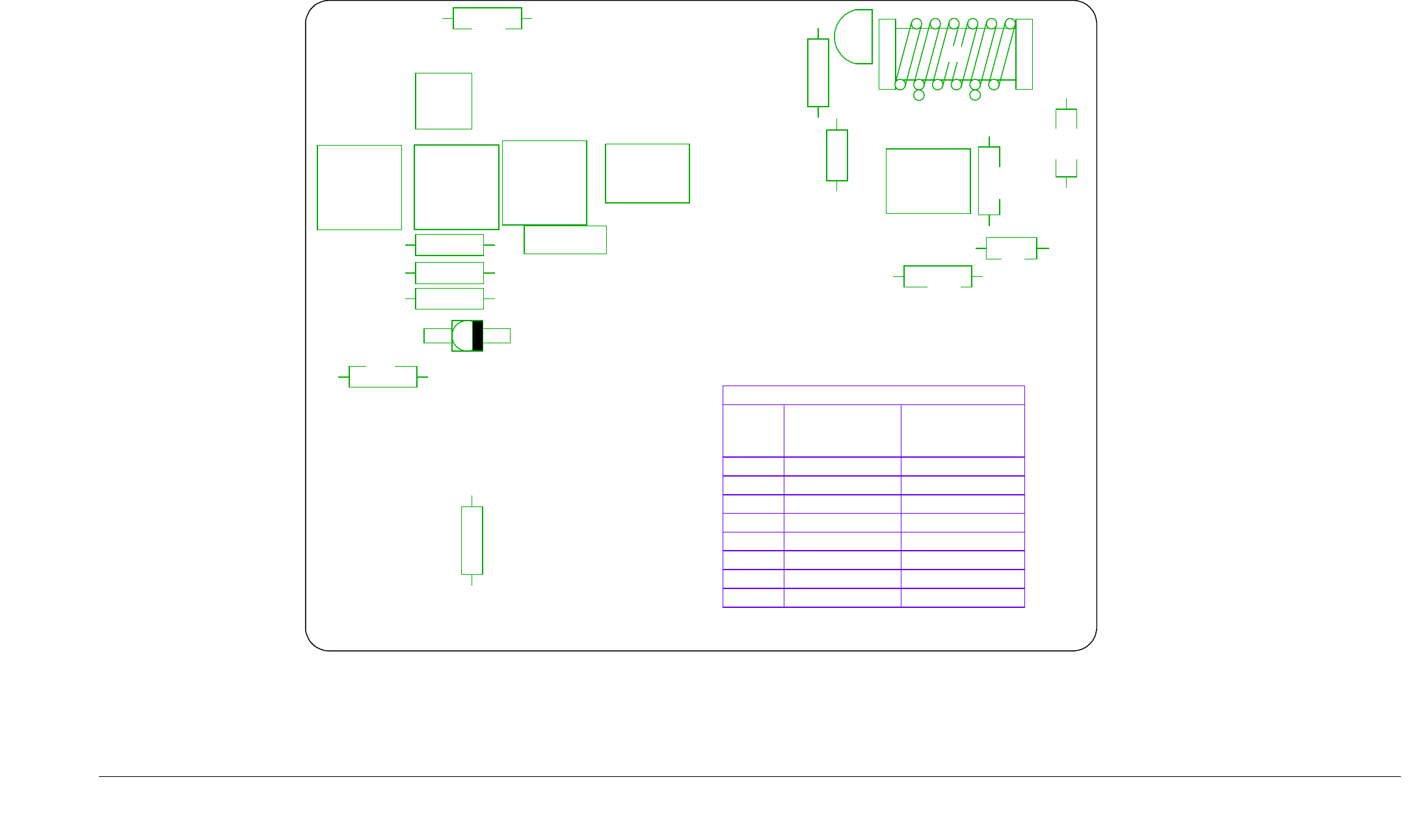
DATE: APR 18, 1999
DWG No:TBA
DANIELS
ELECTRONICS VICTORIA, B.C.
TITLE: OS-3A130 ANALOG BOARD OUTLINE
BOARD No.:
DWG REV DATE: 04 NOV 99
50082-04
DWG No:TBA
TITLE: OS-3A130 ANALOG BOARD BOTTOM THROUGH HOLE LAYOUT
L4
1.5µH
L6
1.5uH
R26
1R2
L8
1.5uH
L3
10uH
L2
10uH
C42
22uF
+
C45
SEL
L7
1.5uH
C37
SEL
C39
SEL
L5
R2
330R
C38
SEL
C49 SEL
R36
R32
R33
SEL
680R
SEL
LED1
+
AM TX
118 - 138 MHz
OS - 3A128
AM RX
139.4 - 159.4 MHz
OS - 3A149
DESIG.
C39
C45
C49
R32
R36
SELECT COMPONENTS
NOT INSTALLED
22 nF2.2 nF
1.0 µF
330 nF 470 nF
15K68K
1K88K2
C38 100 nF 1.0 µF
C37 470 nF 1.0 µF
Q5
J211
- --
L13
1.5uH
C63
680nF
DWG No:TBA
TITLE: OS-3A130 ANALOG BOARD BOTTOM THROUGH HOLE DESIGNATIONS
Enhanced AM/FM Synthesizer Instruction Manual OS(R/T)-3(A/H) 29 - 470 MHz 4-5
4.2 OS(R/T)-3A 118 - 159.4 MHz Analog Board Diagrams
4.2.1 OS(R/T)-3A 118 - 159.4 MHz Analog Board Component Layout (Bottom) PCB 50082-04
OS3150M1A
DE DANIELS
ELECTRONICS
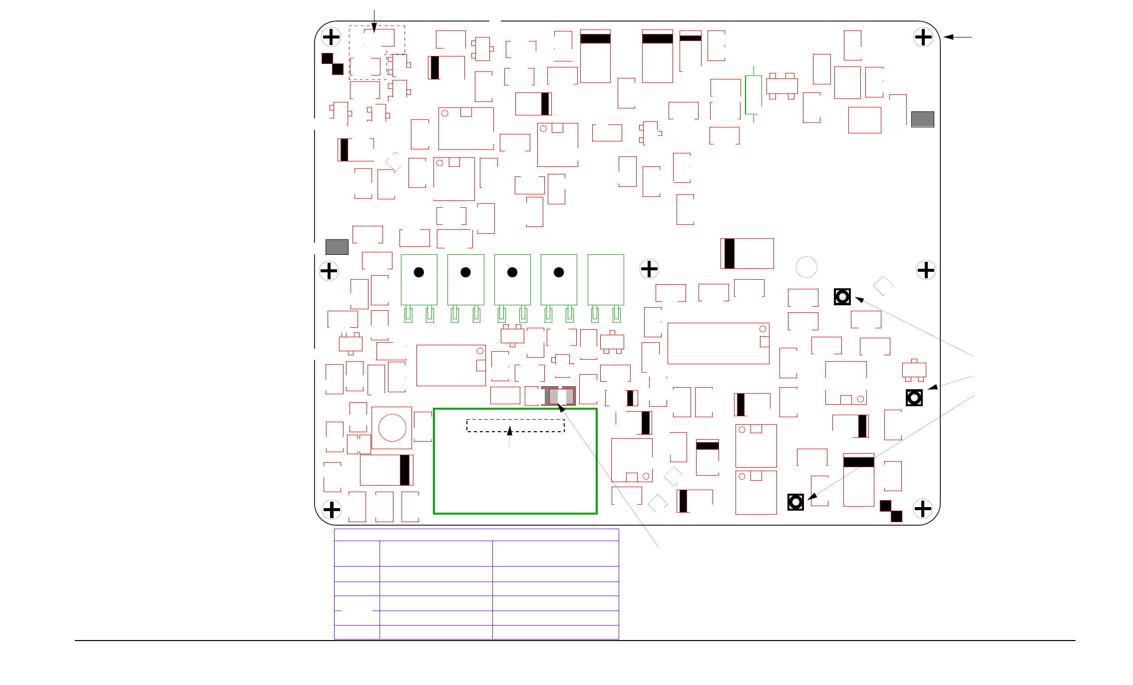
DATE: APR 18, 1999
DWG No:OS3AxxxxxS1A
DANIELS
ELECTRONICS VICTORIA, B.C.
TITLE: OS-3A130 ANALOG BOARD OUTLINE
BOARD No.:
DWG REV DATE: 04 NOV 99
50082-04
Not Inastalled (installed during final assembly)
DWG No:OS3AxxxxxS1A
TITLE: OS-3A130 ANALOG BOARD SURFACE MOUNT LAYOUT
C51
R14
10k0
R13
11k8
C6
47µF
C2
1nF
C7
10nF
C12
U6
LT1129-IS8
4.7µF
Q1
BC817
R3
10k0
C3
1nF
R4
10k0
R34
10k010k0
R35
10k0
C19
10nF
R23
10R0
U7
LP2951
U8
LP2951
U10
MC145191
C21
10nF
C22
10nF C20
4.7µF
C29
47µF
C30
10nF
R29
18k2
U9
SI9945DY
R15
10R010R0
R24
10R0
4.7µF
C13
4.7µF
C15
4.7µF
C27
4.7µF
R12
10k0
1µF C22
10nF
C26
1nF
R10
10k0
10k0
R18 C11
Q3
BC807
100nF
C5
Q4
BC817
100k
R53
47µF
C18
100k
R42
10k0
R19
D5
BAS16
JU1
1nF
C16
5k11
R17
5k11
R16
100nF
C8 100R
R5R5
5k0
RV1
C26
1nF
C31
R9
1k00
R6
1k00 R7
10k0
C50
100nF
Q2
BC817
R8
10k0
10nF
C9
N/I
C25
49R9
R1
10R0
R25
10nF
C4
0R0
R39
D1 D2
MMBV609L
MMBV609L
10R0
R20
SEL
C23
11k8
R27
C28
6.8µF
MMBD701L
SEL
C40
D3
C34
10nF
C35
5.6pF
C36
3.3pF
R31
49R9
R30
10R0
100nF
C47
330pF
R41
20k0
C52
10nF
C41
R28
N/I
MSA-0611
U11
47nH
L12
47nH
L11
27pF
C59
27pF
47pF
C58
27pF
C44
330pF C53
C46
100nF
18R2
R45
10nF
R44
1k82
R46
475R
D4
BYD17J
D6
SEL
4.7µF
C61
10nF
C62 274K
R57 4k75
R62
C60
2.2µF
U17
LTC1275I
U19
MC33172
U18
PIC12C672
SEL
R60
R58
825K
R59
10K0
R63
10R0
137k
R43
R37
49k9
100µF
C32 100µF
C33
D7
SEL
1nF
C1
1nF
C17
100nF
C48
10nF
C14
U20
74HC14 100nF
C10
137k
R22
10k
R11
100nF
R38
49k9
JU2
20K0
R61
1nF
C24
Q6
MMBR901
C43
Factory Installed Jumpers
DWG No:OS3AxxxxxS1A
TITLE: OS-3A130 ANALOG BOARD SURFACE MOUNT DESIGNATIONS
DWG No:OS3AxxxxxS1A
TITLE: OS-3A130 ANALOG BOARD TOP THROUGH HOLE LAYOUT
U2
OPL950 U3
OPL950 U4
OPL950 U1
OPL950 U5
OP140A
TCXO1
R40
SEL
C23
C40
SELECT COMPONENTS
AM TX 118 -138 MHz
OST - 3A128
3.3pF
8.2pF
Not Installed
SMV1211
Not Installed
D6,D7
330Ω220ΩR40
AM RX 118 -138 MHz
OSR - 3A149
D6,D7 SMV1211-001D6,D7 D6-SMV1212-004, D7-N/I
DWG No:OS3AxxxxxS1A
TITLE: OS-3A130 ANALOG BOARD TOP THROUGH HOLE DESIGNATIONS
68K139K2R60
DE DANIELS
ELECTRONICS
BAR located on
bottom side of TCXO
4-6
4.2.2 OS(R/T)-3A 118 - 159.4 MHz Analog Board Component Layout (Top) PCB 50082-04
TP2
TP3
TP1
TP4
Enhanced AM/FM Synthesizer Instruction Manual OS(R/T)-3(A/H) 29 - 470 MHz
OS3150M2A
Desolder three board
interconnect points to
separate analog and
digital boards..
Remove seven M2.0
machine screws to
remove analog board.
Select values
AB
JU1 POSTION B SELECTED
FOR INTERNAL 9.6 MHz
P2
P1
P3
LOCK DETECT
LED
J1
J2
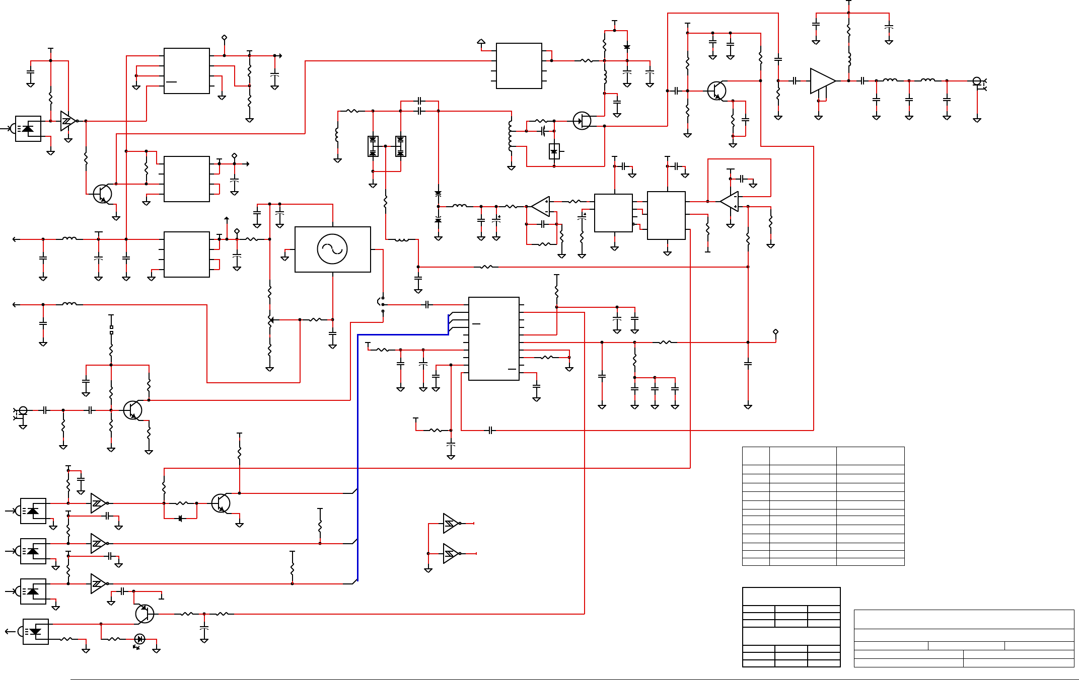
DESIG.
C23 *
C45
C39
R36
R32
C49
C40 *
C37
C38
10 pF
NOT INSTALLED
8K2
68K
2.2 nF
NOT INSTALLED
470 nF
100 nF
NOT INSTALLED
1.0 µF
1K8
15K
22 nF
8.2 pF
1.0 µF
1.0 µF
AM RX 139.4-159.4 MHz
OSR-3A149
* - Surface Mount Components
D6*, D7* SMV1211-001 D6 - SMV1212-004, D7 - N/I
R60 * 39K2 68K1
AM TX 118-138 MHz
OST-3A128
C45 330 nF 470 nF
R40 330R 330R
VICTORIA B.C.
DE
DANIELS
ELECTRONICS
DE
DANIELS
ELECTRONICS
4
.
2
.
3
O
S
(
R
/
T
)-
3
(
A
/
H
)
118
-
159
.
4
MH
z
A
na
l
og
B
o
ard
S
c
h
e
m
a
t
i
c
D
i
a
g
ra
m
TITLE: OS(R/T)-3(A/H) 118 - 159.4 MHz ANALOG BOARD SCHEMATIC DIAGRAM
BOARD No: 50082-04
TP4 LOOP CONTROL
SET FOR ≈3.3 VDC
DWN BY: STAN POLYAKOV
C63
DWG REV DATE: 08 AUGUST 1999
R54-R56
R21, R47-R52
U12 - U16
L1, L9, L10C54 - C57
U20
R63Q6
L13D7
DATE: 06 JULY 99
BOARD REV: 1
C32 AND C33 ARE SURFACE MOUNT
OR THROUGH HOLE PARTS
TO ALL +5VB SUPPLY POINTS
TO ALL +5VA SUPPLY POINTS
DWG No: OS3150M3A
Enhanced AM/FM Synthesizer Instruction Manual OS(R/T)-3(A/H) 29 - 470 MHz 4-7
A
B
TCXO1RV1
LED1
APRVD:
----- -----
-----
-----
UNUSED REFERENCE DESIGNATORS
HIGHEST REFERENCE DESIGNATORS
RF OUTPUT
LOCK DETECT
OUTPUT
ACTIVATED WHEN
UNLOCKED
NC
NC
NC
POWER CNTRL
ID≈10 mA
LOCK DETECT
DATA INPUT
CLK
ENABLE
ACTIVE HIGH
TO ALL +8VA SUPPLY POINTS
EXTERNAL REFERENCE
INPUT (50Ω)
FREQ CONTROL
TCXO MOD INPUT
+9.5 VDC SUPPLY
NC
NC
REFOUT
LD
øR
øV
VPD
PDOUT
GND
RX
TEST 1
FIN
REFIN
DIN
CLK
ENB
OUTPUTA
OUTPUTB
VDD
TEST 2
VCC
FIN
1
2
3
4
5
6
7
8
9
1011
12
13
14
15
16
17
18
19
20
MC145191
U10
AGND
AGND
GND
VCNTRL
OUTPUT
VCC
1
4
2
3
TCXO1
9.6 MHz
AGND
C31
1.0nF
OUTPUT
SENSE
5VTAP
FB
INPUT
ERROR
SHDN
GND
1
2
6
74
3
5
8
U8
LP2951
AGND
+
C15
4.7uF
AGND
R15
10R0
+
C18
47uF
AGND
R16
5K11
R17
5K11
AGND
32
1
RV1
5K0
AGND
C16
1.0nF
+
C6
47uF
AGND
AGND
C7
10nF
R19
10K0
C14
10nF
AGND
2
1
3
JU1
C19
10nF
+5VA
Z2
AGND
C22
10nF
AGND
C21
10nF
R23
10R0
R24
10R0
+
C27
4.7uF
AGND
+
C20
4.7uF
AGND
+5VA
+5VA
GS
D
Q5
J211
AGND
C34
10nF
AGND
L7
1.5uH
+
C32
100uF
AGND
R30
10R0
+8VA
AGND
L8
1.5uH
+
C42
22uF
AGND
C43
10nF
AGND
+8VA
C44
330pF
L11
47nH L12
47nH
C53
27pF C58
47pF C59
27pF
AGND
AGND
AGND
0
1
J2
AGND
2
1
3D2
MMBV609L
2
1
3
D1
MMBV609L
L4
1.5uH
R20
10R0
AGND
R25
10R0
C25
SEL
AGND
C23
SEL
L2
10uH
AGND
C2
1.0nF
P2
OUTPUT
SENSE
5VTAP
FB
INPUT
ERROR
SHDN
GND
1
2
6
74
3
5
8
U7
LP2951
AGND
+
C13
4.7uF
AGND
L3
10uH
AGND
C3
1.0nF
P3
E
B
C
Q2
BC817
J1
R7
10K0
R6
1K00
R9
1K00
AGND
AGND
C4
10nF
C9
10nF
AGND
R1
49R9
AGND
R5
100R
C8
100nF
AGND
+5VA
AGND
AGND
AGND
AGND
AGND
R13
11K8
R14
10K0
AGND
+
C12
4.7uF
AGND
Z1
+8VA
AGND
+5VB
AGND
+5VB
TP1
TP2
TP3
E
B
C
Q1
BC817
AGND
R4
10K0 R3
10K0
OUTPUT
ADJ
GND
NC
VIN
GND
GND
SHDN
8
7
6
5 4
3
2
1
LT1129-IS8
U6
+
C33
100uF
AGND
D4
BYD17J
R26
1R2
E
B
C
Q4
BC817
R11
10K0
AGND
+5VA
1
2
OP140A
U5
R12
10K0
AGND
AGND
E
B
CBC807
Q3
R10
10K0
R2
330R
C45
SEL
R36
SEL
C37
SEL
AGND
R28
N/I
+
C29
47uF
AGND
AGND
C30
10nF
AGND
1.0nF
C26
D1
D1
D2
D2
S1
G1
S2
G2
1
2
3
4 5
6
7
8
SI9945DY
U9
AGND
0
R39
R8
10K0
10K0
R34
+5VA
+5VA
SEL
C49
AGND
+
1.0uF
C11
BAS16
D5
SEL
R32 TP4
C38
SEL C39
SEL
AGND
AGND
SEL
C40
DIN
AGND
R33
680R
AGND
1
2
C62
10nF
AGND
AGND
4
3
2
1
8
U19
MC33172
6
5
7
U19
MC33172
b
1
2
R61
20K0
12
R59
10K0
AGND
1
2
C60
2.2uF
1
2
R63
10R0
AGND
AGND
VOUT
REF
CLK
DOUT
DIN
LOAD
GND
VCC
1
2
3
4
5
6
7
8
U17
LTC1257I
AGND
R27
11K8
+
C28
6.8uF 1
3
2
MMBD701L
D3
+5VB
+5VB
1
2
R58
825K0
AGND
AGND
GP5 GP2
GP3
GND
VDD
GP0
GP4
GP1
7
4
8
6
1
3
52
PIC12C672
U18
IN OUT
GND
1 3
4 2
U11
MSA-0611
+5VA
49K9
R38
49K9
R37
9.5V
9.5V
L6
1.5uH
AGND
1 21.0nF
C17
1 2 1.0nF
C1
AGND
1 2
1.0nF
C24
AGND
1 2
R60
SEL
A
C
U1
OP950 21 14
7
U20
74HC14
a
AGND
A
C
U2
OP950
A
C
U3
OP950
A
C
U4
OP950
1
2
JU2
43
U20
74HC14
b
65
cU20
74HC14
89
dU20
74HC14
AGND
C5
100nF
LED1
C10
100nF
10K0
R35
R18
10K0
1011
74HC14
U20e
1213
74HC14
U20f
AGND
ENB
CLK
DIN
CLK
ENB
1 2
330pF
C47
R40
330R (SEL)
1
2
100nF
C48
AGND
AGND
1 2
100nF
C50
1 2 100nF
C51
+5VA
E
B
C
MMBR901
Q6
AGND
+8VA
1
21K82
R44 1
2
18R2
R45
AGND
AGND
1
2
475R0
R46
1 2
3.3pF
C36
1
2
5.6pF
C35
1
2
100nF
C41
AGND
1
2
10nF
C46
C52
10nF
AGND
1 2
R62
4K75
AGND
A
K
D6
SEL
A
K
D7
SEL
1
4
3
2
L5
AGND
+5VB
+5VB
+5VB
L13
1.5uH
1
24.7uF
C61 1 2
680nF
C63
1
2
R22
137K0
1
2
R42
100K0
1
2
R43
137K0
1
2
R53
100K0
1
220K0
R41
1
2SM_0805
100R0
R31
+5VA
1
2
R57
274K0
R29
18K2

DE
DANIELS
ELECTRONICS
4-8
Enhanced AM/FM Syn
thesizer Instruction Manual OS(R/T)-3(A/H) 29 - 470 MHz
This Page Intentionally Left Blank
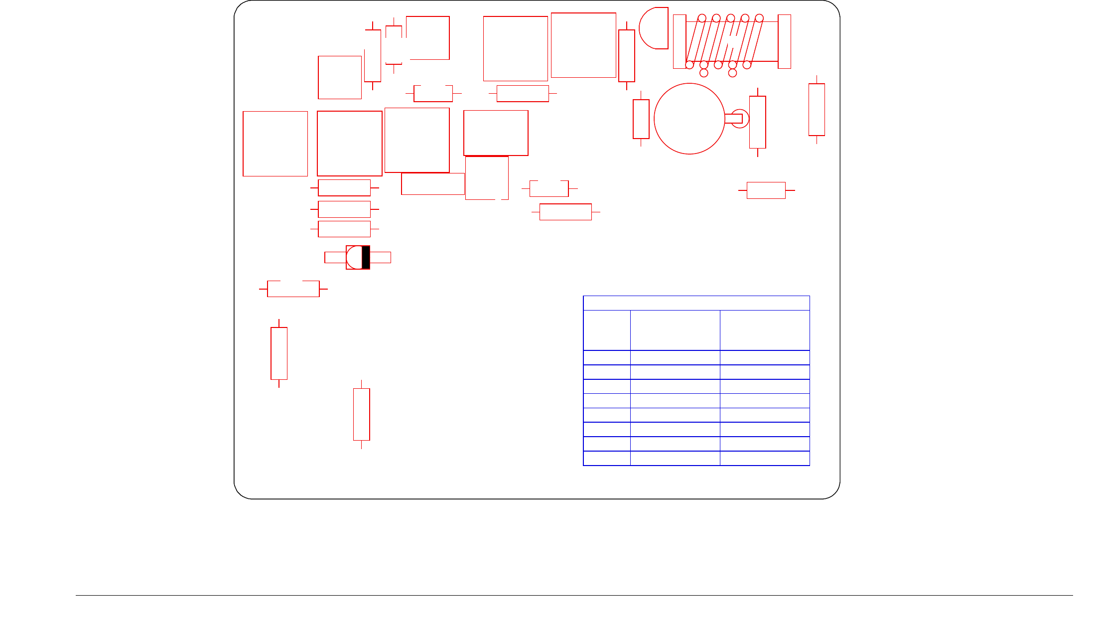
PCB 50025-02
DATE: MARCH 22, 1996
DWG No:TBA
DANIELS
ELECTRONICS VICTORIA, B.C.
TITLE: OS-3H ANALOG BOARD THROUGH HOLE BOTTOM LAYOUT
BOARD No.:
DWG REV DATE: 15 MARCH 2000
50025-02
L5
C33
100µF
C32
100µF
L4
1.5µH
L6
1.5µH
R26
1R2
1.5µH
L8
1.5µH
L10
1.5µH
L3
10uH
L2
10µH
R51
220R
C54
22µF
+C50
22µF
+
++
C42
22µF
+
R50
180R
R40
180R
C45
SEL
L7
1.5µH
C24
1-14pF
C37
1.0 µF
C39
SEL
L1
10µH
R2
330R
C38
SEL
C49 SEL
R36
R32
R33
SEL
680R
SEL
LED1
+
TITLE: OS-3H ANALOG BOARD THROUGH HOLE BOTTOM DESIGNATION
L9
VHF LOW BAND
128 - 153 MHz
OSx - 3H141
VHF HIGH BAND
150 - 174 MHz
OSx - 3H162
DESIG.
C39
22 nF
C45
33 nF
NOT INSTALLED
C49
220 nF
15K12KR32
6K22K2R36
SELECT COMPONENTS
C38 1.0 µF 470 nF
1.0 µF
470 nF
Q5
J211 L5
Enhanced AM/FM Synthesizer Instruction Manual OS(R/T)-3(A/H) 29 - 470 MHz 4-9
4.3 OS(R/T)-3H 128 - 174 MHz Analog Board Diagrams
4.3.1 OS(R/T)-3H 128 - 174 MHz Analog Board Component Layout (Bottom)
OS3150M1B
DE DANIELS
ELECTRONICS
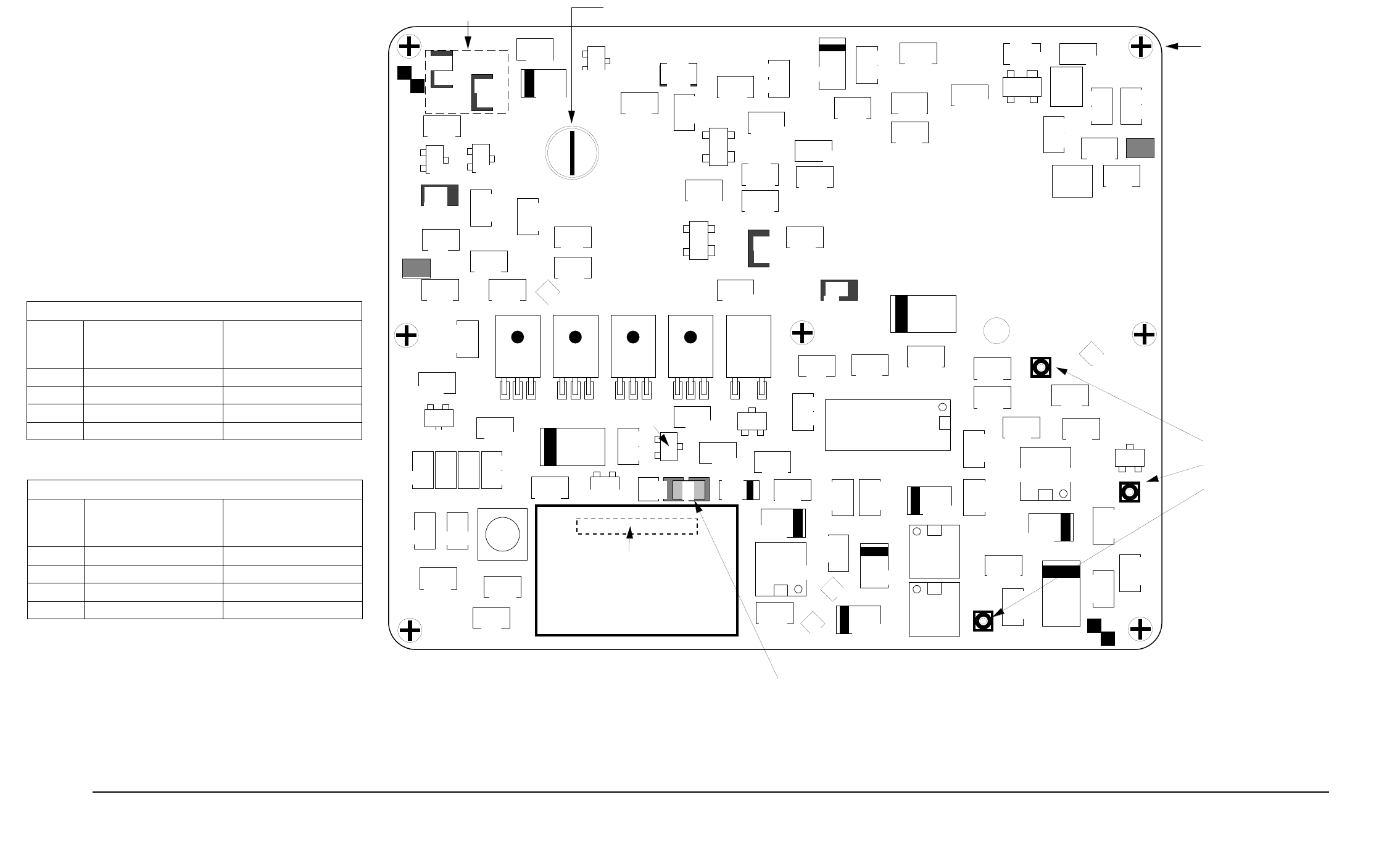
PCB 50025-02
DATE: FEB 24, 1996
DWG No:OS3HANA150AS1A
DANIELS
ELECTRONICS VICTORIA, B.C.
TITLE: OS-3H150 ANALOG BOARD ECO #584 CHANGES
BOARD No.:
DWG REV DATE: June 19, 2000
50025-02
Factory Installed Jumpers
Select components
TITLE: OS-3H150 ANALOG BOARD SURFACE MOUNT TOP DESIGNATIONS
C1
1nF
R14
10k0
R13
11k8
C6
47µF
C2
1nF
C7
10nF
C12
U6
LT1129-IS8
4.7µF
Q1
BC817
R3
10k0
C3
1nF
R4
10k0
R34
10k010k0
R35
10k0
C19
10nF
R23
10R0
U7
LP2951
U8
LP2951
U10
MC145193
C21
10nF
C22
10nF C20
4.7µF
C29
47µF
C30
10nF
R29
3k92
U9
SI9945DY
R15
10R010R0
R24
10R0
4.7µF
C13
4.7µF
C15
4.7µF
C27
4.7µF
R12
10k0
1µF C22
10nF
C26
1nF
R10
10k0
10k0
R18
C11
Q3
BC807
100nF
C5
Q4
BC817
10k0
R11
47µF
C18
100nF
C10
10k0
R19 D5
BAS16
JU1
1nF
C16
5k11
R17
5k11
R16
100nF
C8
100R
R5R5
5k0
RV1
C26
1nF
C31
R9
1k00 R6
1k00
R7
10k0
C14
10nF
Q2
BC817
R8
10k0
10nF
C9
1nF
C25
49R9
R1
20k0
R21
10k0
R53
10R0
R25
10nF
C4
1nF
C17 0R0
R39
R22
D1 D2
MMBV609L
N/I
10R0
R20
SEL
C23 11k8
R27
C28
6.8µF
MMBD701L
SEL
C40
D3
10nF
C34
10nF
C35
SEL
C36
330pF
R31
49R9
R30
10R0
C44
330pF
C47
330pF
R4118R2
R47
47R5
R48
47R5
R49
10R0
C44
C55
10nF
R52
N/I
C56
330pF R28
N/I
U11
MSA-0611
U16
MSA-0611MSA-0611
MSA-0611
U15
47nH
L12
47nH
L11
27pF
C59
27pF
274R
R55
274R
R56
18R2
R54
47pF
C58
27pF
C52
330pF C53
C46
330pF330pF
C51
10nF
27R4
R45
10nF
C43
47R5
R44
47R5
R46
33R2
D4
BYD17J
DWG No:OS3HANA150AS2B
SEL
TITLE: OS-3H ANALOG BOARD THROUGH HOLE LAYOUT
DWG No:OS3HANA150AT1
U2
OPL550 U3
OPL550 U4
OPL550 U1
OPL550 U5
OP140A
TITLE: OS-3H ANALOG BOARD THROUGH HOLE DESIGNATION
DWG No:OS3HANA150AT2
DE DANIELS
ELECTRONICS
C24 Fine Frequency Adjust
BAR located on
bottom side of TCXO
4-10
4.3.2 OS(R/T)-3H 128 - 174 MHz Analog Board Component Layout (Top)
TP2
TP3
TP1
TP4
Enhanced AM/FM Synthesizer Instruction Manual OS(R/T)-3(A/H) 29 - 470 MHz
OS3150M2C
Desolder three board
interconnect points to
separate analog and
digital boards..
Remove seven M2.0
machine screws to
remove analog board.
Select values
AB
JU1 position B Selected
for internal 9.6 MHz
P2
P1
P3
LOCK DETECT
LED
J1
J2
SEL
C35
R22 0R0
100R
Receiver
128 - 174 MHz
OSR - 3Hxxx
Transmitter
128 - 174 MHz
OST - 3Hxxx
SELECT COMPONENTS
C23
C40 12 pF 6.8 pF
6.8 pF
12 pF
VHF HIGH BAND
150 - 174 MHz
OSx - 3H162
C35 3.3 pF 8.2 pF
VHF LOW BAND
128 - 153 MHz
OSx - 3H141
SELECT COMPONENTS
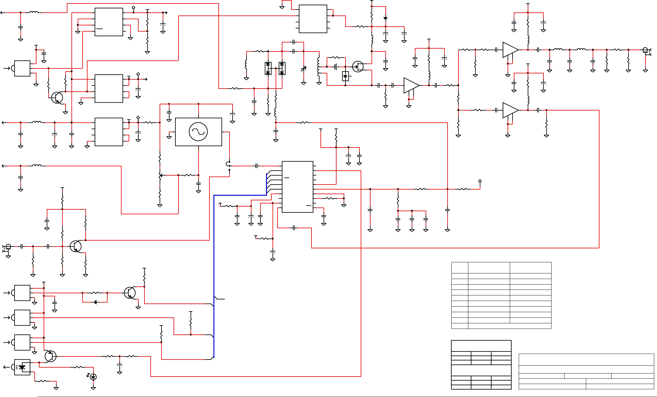
DESIG. LOW BAND 128-153 MHz
OSx-3H141
C23 * 12 pF 6.8 pF
C45 470nF 220 nF
C39 1.0uF Not Installed
R36 2K2 6K2
R32 12K 15K
C49 33nF 22nF
C40 * 12 pF 6.8 pF
C38 1.0 µF 470 nF
HIGH BAND 150-174 MHz
OSx-3H162
* - Surface Mount Components
C35 * 3.3 pF 8.2 pF
R22 * 100R for OST-3Hxxx / 0R0 for OSR-3Hxxx
VICTORIA B.C.
DE
DANIELS
ELECTRONICS
DE
DANIELS
ELECTRONICS
DWG No: OS3150M3C DWG REV DATE: 19 JUN 00
4
.
3
.
3
O
S
(
R
/
T
)-
3
H
128
-
174
MH
z
A
na
l
og
B
o
ard
S
c
h
e
m
a
t
i
c
D
i
a
g
ra
m
TITLE: OS(R/T)-3(A/H) 128.6 - 174 MHz ANALOG BOARD SCHEMATIC DIAGRAM
TP4 LOOP CONTROL
SET FOR ≈ 2.3 VDC
4-11
Enhanced AM/FM Synthesizer Instruction Manual OS(R/T)-3(A/H) 29 - 470 MHz
A
B
U12 - U14R42,R43
R37,R38C57C41,C48
U16TCXO1RV1
R56Q5LED1
L12D5C59
BOARD REV: 2BOARD No: 50025-02
DWN BY: COLIN GUNNDATE: 21 FEB 96 APRVD:
----- -----
-----
-----
UNUSED REFERENCE DESIGNATORS
HIGHEST REFERENCE DESIGNATORS
RF OUTPUT
3.5 dB Pad
LOCK DETECT
OUTPUT
ACTIVATED WHEN
UNLOCKED
NC
NC
NC
MODULATION INPUT
POWER CNTRL
ID≈10 mA
LOCK DETECT
DATA INPUT
CLK
ENABLE
ACTIVE HIGH
TO ALL +8VA SUPPLY POINTS
EXTERNAL REFERENCE
INPUT (50Ω)
FREQ CONTROL
TCXO MOD INPUT
+9.5 VDC SUPPLY
TO ALL +5VA SUPPLY POINTS
NC
NC
REFOUT
LD
øR
øV
VPD
PDOUT
GND
RX
TEST 1
FIN
REFIN
DIN
CLK
ENB
OUTPUTA
OUTPUTB
VDD
TEST 2
VCC
FIN
1
2
3
4
5
6
7
8
9
1011
12
13
14
15
16
17
18
19
20
U10
MC145193
AGND
AGND
GND
VCNTRL
OUTPUT
VCC
1
4
2
39.6 MHz
TCXO1
AGND
1.0nF
C31
3K92
R29
OUTPUT
SENSE
5VTAP
FB
INPUT
ERROR
SHDN
GND
1
2
6
74
3
5
8
LP2951
U8
AGND
+
4.7uF
C15
AGND
10R0
R15
+
47uF
C18
AGND
5K11
R16
5K11
R17
AGND
32
1
5K0
RV1
AGND
1.0nF
C16
+
47uF
C6
AGND
AGND
10nF
C7
10K0
R19
10nF
C14
AGND
2
1
3
JU1
10nF
C19
+5VA
Z2
AGND
10nF
C22
AGND
10nF
C21
10R0
R23
10R0
R24
+
4.7uF
C27
AGND
+
4.7uF
C20
AGND
+5VA
+5VA
GS
D
J211
Q5
SEL
C35
49R9
R31
AGND
11K8
R27
1
4
3
2
L5
AGND
+
6.8uF
C28
10nF
C34
AGND
1
3
2
D3
MMBD701L
1.5uH
L7
+
100uF
C32
AGND
10R0
R30
330pF
C36
C24
1-14pF
AGND
+8VA
AGND
IN OUT
GND
1 3
4 2
MSA-0611
U11
180R
R40
1.5uH
L8
+
22uF
C42
AGND
10nF
C43
AGND
+8VA
330pF
C44 18R2
R41
47R5
R44
47R5
R47
33R2
R46
AGND
330pF
C46
AGND
IN OUT
GND
1 3
4 2
MSA-0611
U15
180R
R50
1.5uH
L9
+
22uF
C50
AGND
10nF
C51
AGND
+8VA
330pF
C52
27R4
R45
330pF
C47
AGND
IN OUT
GND
1 3
4 2
MSA-0611
U16
220R
R51
1.5uH
L10
+
22uF
C54
AGND
10nF
C55
AGND
+8VA
330pF
C56
47R5
R48
10R0
R49
AGND
N/I
R52
AGND
47nH
L11 47nH
L12
27pF
C53 47pF
C58 27pF
C59
AGND
AGND
AGND
274
R55
AGND
18R2
R54
274
R56
AGND
J2
AGND
2
1
3
MMBV609L
D2
2
1
3
N/I
D1
1.5uH
L4
10R0
R20
AGND
10R0
R25
1.5uH
L6
1.0nF
C25
AGND
SEL
C23
10uH
L2
AGND
1.0nF
C2
P2
OUTPUT
SENSE
5VTAP
FB
INPUT
ERROR
SHDN
GND
1
2
6
74
3
5
8
LP2951
U7
AGND
+
4.7uF
C13
AGND
10uH
L3
AGND
1.0nF
C3
P3
E
B
C
BC817
Q2
J1
10K0
R7
1K00
R6
1K00
R9
AGND
AGND
10nF
C4 10nF
C9
AGND
49R9
R1
AGND
100R
R5
100nF
C8
AGND
+5VA
VCC
OUT
GND
1
2
3
OPL550
U1
VCC
OUT
GND
1
2
3
OPL550
U2
VCC
OUT
GND
1
2
3
OPL550
U3
VCC
OUT
GND
1
2
3
OPL550
U4
AGND
AGND
AGND
+5VA
100nF
C10
AGND
OUTB
OUTA
ENB
CLK
DIN
AGND
AGND
11K8
R13
10K0
R14
AGND
+
4.7uF
C12
AGND
Z1
+8VA
AGND
+5VB
100nF
C5
AGND
+5VB
TP1
TP2
TP3
E
B
C
BC817
Q1
AGND
10K0
R4
10K0
R3
OUTPUT
ADJ
GND
NC
VIN
GND
GND
SHDN
8
7
6
5 4
3
2
1
U6
LT1129-IS8
+
100uF
C33
AGND
BYD17J
D4
1R2
R26
AGND
E
B
C
BC817
Q4
10K0
R11
AGND
10K0
R18
+5VA
ENB
CLK
1
2
U5
OP140A
10K0
R12
AGND
AGND
E
B
CQ3
BC807
10K0
R10
330R
R2
SEL
C45
SEL
R36
1.0uF
C37
AGND
+8VA
R28
N/I
+
47uF
C29
AGND
AGND
10nF
C30
OUTB
L1
10uH
AGND
C1
1.0nF
P1
AGND
C17
1nF R22
SEL
AGND
R21
20K0
C26
1.0nF
D1
D1
D2
D2
S1
G1
S2
G2
1
2
3
4 5
6
7
8
U9
SI9945DY
AGND
R39
0R0
10K0
R8
R34
10K0
R35
10K0
+5VA
+5VA
C49
SEL
AGND
+
C11
1.0uF
D5
BAS16
R32
SEL R53
10K0
TP4
SEL
C38 SEL
C39
AGND
AGND
C40
SEL
DIN
LED1
AGND
680R
R33
+5VA

DE
DANIELS
ELECTRONICS
4-12
Enhanced AM/FM Synthesizer Instruction Manual OS(R/T)-3(A/H) 29 - 470 MHz
This Page Intentionally Left Blank
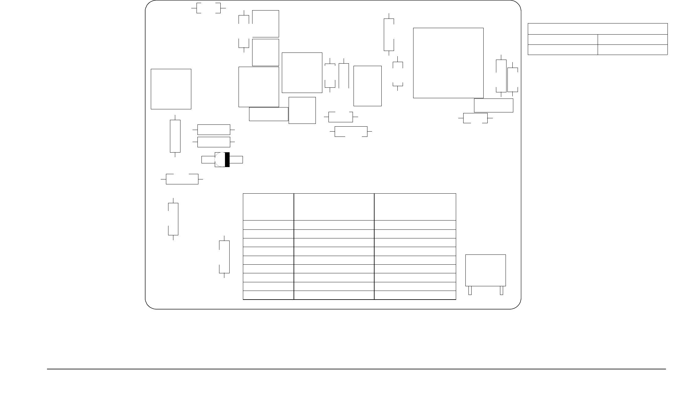
DATE: MARCH 22, 1996
DWG No:TBA
DANIELS
ELECTRONICS VICTORIA, B.C.
TITLE: OS-3H ANALOG BOARD THROUGH HOLE BOTTOM LAYOUT
BOARD No.:
DWG REV DATE: 23 May 2000 (NB)
50028-02
L6
1.5µH
R26
1R2
L9
1.5µH
L8
1.5µH
L10
1.5µH
L3
10µH
L2
10µH
R51
220R
C54
22uF
+C50
22µF
+
++
C42
22µF
+
R50
180R
R40
180R C45
SEL
L7
1.5µH
C37
1µF
C39
SEL
L1
10µH
R2
330R
C38
SEL
C49 SEL
R36 R32
R33
SEL
680R
SEL
LED1
+
TITLE: OS-3H ANALOG BOARD THROUGH HOLE BOTTOM DESIGNATION
U17
VCO
1VCO INSTALLED (U17)
LVCO-2309 TEV VCO-190-435 MT
RX 427.4 - 451.4 MHz TX 406 - 470 MHz
R21
SEL
C16
100nF
DESIGNATION OSR-3H440
RX 427.4 - 451.4 MHz
LVCO-2309 TEV
OST-3H4xx
TX 406 - 470 MHz
VCO-190-435 MT
C37
C38
C39
C45
C49
C60
R21
R32
R36
1.0 µF
1.0 µF
1.0 µF
470 nF
33 nF
Not Installed
Not Installed
4k7
1k5
1.5 µF
1.5 µF
1.5 µF
68 nF
15 nF
0 Ω Wire Jumper
2k7
6k2
1k2
DE DANIELS
ELECTRONICS
Enhanced AM/FM Synthesizer Instruction Manual OS(R/T)-3(A/H) 29 - 470 MHz 4-13
4.4 OS(R/T)-3H 406 - 470 MHz Analog Board Diagrams
4.4.1 OS(R/T)-3H 406 - 470 MHz Analog Board Component Layout (Bottom)
OS3450M1C
PCB 50028-02
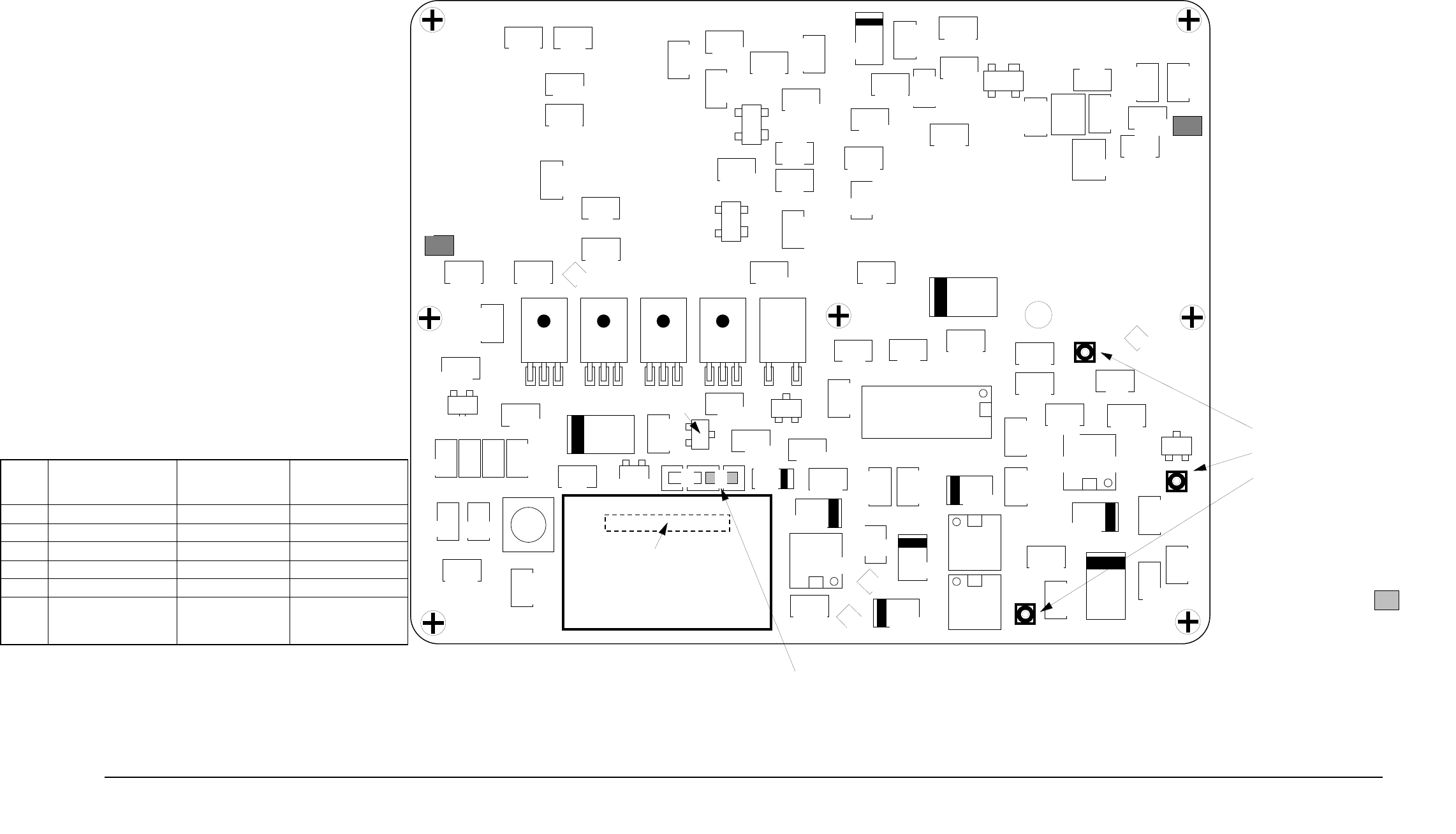
DATE: FEB 24, 1996
DWG No:OS3HANA440AS1
DANIELS
ELECTRONICS VICTORIA, B.C.
TITLE: UHF OS-3H ANALOG BOARD SURFACE MOUNT TOP LAYOUT
BOARD No.:
DWG REV DATE: MAY 23, 2000
50028-02
TITLE: OS-3H UHF ANALOG BOARD SURFACE MOUNT TOP DESIGNATIONS
C1
1nF
R14
10k0
R13
11k8
C6
47µF
C2
1nF
C7
10nF
C12
U6
LT1129-IS8
4.7µF
Q1
BC817
R3
10k0
C3
1nF
R4
10k0
R34
10k010k0
R35
10k0
C19
10nF
R23
10R0
U7
LP2951
U8
LP2951
U10
SEL
C21
10nF
C22
10nF
C20
4.7µF
C29
47µF
C30
10nF
R29
SEL
U9
SI9945DY
R15
10R010R0
R24
10R0
4.7µF
C13
4.7µF
C15
4.7µF
C27
4.7µF
R12
10k0
1µF
C22
10nF
C26
1nF
R10
10k0
10k0
R18
C11
Q3
BC807
100nF
C5
Q4
BC817
10k0
R11
47µF
C18
100nF
C10
0R0
R19
D5
BAS16
JU1
5k11
R17
5k11
R16
100nF
C8
100R
R5R5
5k0
RV1
C26
1nF
C31
R9
1k00
R6
1k00
R7
10k0
C14
10nF
Q2
BC817
R8
10k0
10nF
C9
1nF
C25
49R9
R1
10k0
R53
10nF
C4
1nF
C17
0R0
R39
10R0
R25
10nF
C34
C35
100pF
C36
330pF
R31
274R
R30
10R0
C44
330pF
C47
330pF
R41
18R2
R47
47R5
R48
SEL
R49
SEL
C44
C55
10nF
R52
SEL
C56
330pF
R28
SEL
U11
MSA-0611
U16
MSA-0611MSA-0611
U15
18nH
L12
18nH
L11
C59
10pF
274R
R55
274R
R56
18R2
R54
15pF
C58
10pF
C52
330pF
C53
C46
330pF
C51
10nF
27R4
R45
10nF
C43
47R5
R44
47R5
R46
33R2
D4
BYD17J
R57
18R2
R58
274R
MSA-0611
Factory Installed Jumpers
DWG No:OS3HANA440AS2
* - INDICATES JUMPERED TO 5VA
DESIG
R28
R29
U10
Not Installed *
3k92
MC145202F*
or
MC145193F*
OST-3H418
TX 406 - 430 MHz OST-3H460
TX 450 - 470 MHz
10R0
36k5
MC145190
OSR-3H440
RX 427.4-451.4 MHz
10R0
36k5
MC145190
R48 47R5 27R427R4
R49 10R0 33R233R2
R52 Not Installed 49R949R9
DWG REV DATE: Dec/11/2000
TITLE: UHF OS-3H ANALOG BOARD THOUGH HOLE TOP LAYOUT
U2
OPL550 U3
OPL550 U4
OPL550 U1
OPL550 U5
OP140A
J1
J2
TITLE: UHF OS-3H ANALOG BOARD THOUGH HOLE TOP DESIGNATIONS
TCXO1
DE DANIELS
ELECTRONICS
BAR located on
bottom side of TCXO
4-14
4.4.2 OS(R/T)-3H 406 - 470 MHz Analog Board Component Layout (Top)
Enhanced AM/FM Synthesizer Instruction Manual OS(R/T)-3(A/H) 29 - 470 MHz
OS3450M2B
Desolder three board
interconnect points to
separate analog and
digital boards..
JU1 position B selected
for internal 9.6 MHz
P2
P1
P3
TP3
TP1
TP4
AB
LOCK DETECT
LED
TP2
PCB 50028-02
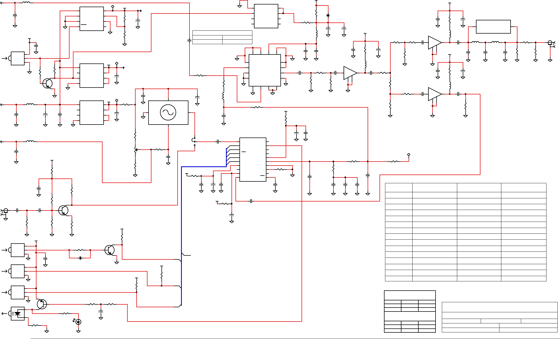
DESIGNATION
OST-3H418
TX 406 - 430 MHz
C38
C39
C45
C49
C60
R32R21
1.5 µF
1.5 µF
68 nF
15 nF
0 Ω Wire Jumper
2k7
OST-3H460
TX 450 - 470 MHz
1.5 µF
1.5 µF
68 nF
15 nF
0 Ω Wire Jumper
2k7
U10 MC145202* or MC145193* MC145190
* - INDICATES JUMPERED TO +5VA
R36R32
R36
6k2
1k2
6k2
1k2
R32
R36
R28
R29
Not Installed *
3k92
10R0
36k5
OSR-3H440
RX 427.4 - 451.4 MHz
1.0 µF
1.0 µF
470 nF
33 nF
Not Installed
Not Installed
MC145190
4k7
1k5
10R0
36k5
R36
R49
R52
10R0
Not Installed
33R2
49R9
R36R48 47R5 27R4
33R2
49R9
27R4
C37 1.5 µF 1.5 µF1.0 µF
VCO INSTALLED (U17)
LVCO-2309 TEV VCO-190-435 MT
RX 427.4 - 451.4 MHz TX 406 - 470 MHz
VICTORIA B.C.
DE
DANIELS
ELECTRONICS
DE
DANIELS
ELECTRONICS
11 DEC 00
DWG No: OS3450M3D
4-15
4
.
4
.
3
O
S
(
R
/
T
)-
3
H
406
-
470
MH
z
A
na
l
og
B
o
ard
S
c
h
e
m
a
t
i
c
D
i
a
g
ra
m
BOARD REV: 2.0
A
B
TITLE: OS(R/T)-3H 406 - 470 MHz ANALOG BOARD SCHEMATIC DIAGRAM
Enhanced AM/FM Synthesizer Instruction Manual OS(R/T)-3(A/H) 29 - 470 MHz
C57, R22
C60
L4, L5
J2, JU1
R58, RV1
BOARD No: 50028-02
U17
R38,R42,R43R20,R27,R37
Q4
D1 - D3
C40,C41,C48C23,C24,C28
U12 - U14
DWG REV DATE:
DATE: 23 MAY 96
TCXO1
LED1
L12D5
DWN BY: COLIN GUNN APRVD:
-----
UNUSED REFERENCE DESIGNATORS
HIGHEST REFERENCE DESIGNATORS
TP4 LOOP CONTROL
SET FOR ≈ 4.5 VDC
RF OUTPUT
3.5 dB Pad
LOCK DETECT
OUTPUT
ACTIVATED WHEN
UNLOCKED
NC
NC
NC
MODULATION INPUT
POWER CNTRL
ID≈10 mA
LOCK DETECT
DATA INPUT
CLK
ENABLE
ACTIVE HIGH
TO ALL +8VA SUPPLY POINTS
EXTERNAL REFERENCE
INPUT (50Ω)
FREQ CONTROL
TCXO MOD INPUT
+9.5 VDC SUPPLY
TO ALL +5VA SUPPLY POINTS
NC
NC
REFOUT
LD
øR
øV
VPD
PDOUT
GND
RX
TEST 1
FIN
REFIN
DIN
CLK
ENB
OUTPUTA
OUTPUTB
VDD
TEST 2
VCC
FIN
1
2
3
4
5
6
7
8
9
1011
12
13
14
15
16
17
18
19
20
U10
SEL
AGND
AGND
GND
VCNTRL
OUTPUT
VCC
1
4
2
39.6 MHz
TCXO1
AGND
1.0nF
C31
SEL
R29
OUTPUT
SENSE
5VTAP
FB
INPUT
ERROR
SHDN
GND
1
2
6
74
3
5
8
LP2951
U8
AGND
+
4.7uF
C15
AGND
10R0
R15
+
47uF
C18
AGND
5K11
R16
5K11
R17
AGND
32
1
5K0
RV1
AGND
100nF
C16
+
47uF
C6
AGND
AGND
10nF
C7
10nF
C14
AGND
2
1
3
JU1
10nF
C19
+5VA
Z2
AGND
10nF
C22
AGND
10nF
C21
10R0
R23
10R0
R24
+
4.7uF
C27
AGND
+
4.7uF
C20
AGND
+5VA
+5VA
100pF
C35
AGND
AGND
10nF
C34
AGND
1.5uH
L7
+
100uF
C32
AGND
10R0
R30
330pF
C36
AGND
+8VA
AGND
IN OUT
GND
1 3
4 2
MSA-0611
U11
180R
R40
1.5uH
L8
+
22uF
C42
AGND
10nF
C43
AGND
+8VA
330pF
C44 18R2
R41
47R5
R44
47R5
R47
33R2
R46
AGND
330pF
C46
AGND
IN OUT
GND
1 3
4 2
MSA-0611
U15
180R
R50
1.5uH
L9
+
22uF
C50
AGND
10nF
C51
AGND
+8VA
330pF
C52
27R4
R45
330pF
C47
AGND
IN OUT
GND
1 3
4 2
MSA-0611
U16
220R
R51
1.5uH
L10
+
22uF
C54
AGND
10nF
C55
AGND
+8VA
330pF
C56
AGND
18nH
L11 18nH
L12
10pF
C53 15pF
C58 10pF
C59
AGND
AGND
AGND
274R
R55
AGND
18R2
R54
274R
R56
AGND
0
1
J2
AGND
AGND
10R0
R25
1.5uH
L6
1.0nF
C25
AGND
10uH
L2
AGND
1.0nF
C2
P2
OUTPUT
SENSE
5VTAP
FB
INPUT
ERROR
SHDN
GND
1
2
6
74
3
5
8
LP2951
U7
AGND
+
4.7uF
C13
AGND
10uH
L3
AGND
1.0nF
C3
P3
E
B
C
BC817
Q2
J1
10K0
R7
1K00
R6
1K00
R9
AGND
AGND
10nF
C4 10nF
C9
AGND
49R9
R1
AGND
100R
R5
100nF
C8
AGND
+5VA
VCC
OUT
GND
1
2
3
OPL550
U1
VCC
OUT
GND
1
2
3
OPL550
U2
VCC
OUT
GND
1
2
3
OPL550
U3
VCC
OUT
GND
1
2
3
OPL550
U4
AGND
AGND
AGND
+5VA
100nF
C10
AGND
OUTB
OUTA
ENB
CLK
DIN
AGND
AGND
11K8
R13
10K0
R14
AGND
+
4.7uF
C12
AGND
Z1
+8VA
AGND
+5VB
100nF
C5
AGND
+5VB
TP1
TP2
TP3
E
B
C
BC817
Q1
AGND
10K0
R4
10K0
R3
OUTPUT
ADJ
GND
NC
VIN
GND
GND
SHDN
8
7
6
5 4
3
2
1
U6
LT1129-IS8
+
100uF
C33
AGND
BYD17J
D4
1R2
R26
AGND
E
B
C
BC817
Q4
10K0
R11
AGND
10K0
R18
+5VA
ENB
CLK
1
2
U5
OP140A
10K0
R12
AGND
AGND
E
B
CQ3
BC807
10K0
R10
330R
R2
SEL
C45
SEL
R36
SEL
C37
AGND
+8VA
SEL
R28
+
47uF
C29
AGND
AGND
10nF
C30
OUTB
L1
10uH
AGND
C1
1.0nF
P1
AGND
C17
1.0nF
R21
SEL
C26
1.0nF
D1
D1
D2
D2
S1
G1
S2
G2
1
2
3
4 5
6
7
8
U9
SI9945DY
AGND
R39
0R0
10K0
R8
R34
10K0
R35
10K0
+5VA
+5VA
C49
SEL
AGND
+
C11
1.0uF
D5
BAS16
R32
SEL R53
10K0
TP4
SEL
C38 SEL
C39
AGND
AGND
DIN
LTL-93BEK1
LED1
AGND
680R
R33
AGND
AGND
AGND
AGND
Band Pass Filter
(Optional)
1 2
F1
GND
MOD I/P
GND
GND
GND MOD GND GND
GND
RF OUT
GND
GND
GND VCCGND GND
VCO
1
2
3
4
5678
9
10
11
12
13141516
U17
R58
274R
R57
18R2
R31
274R
SEL
C60
SEL
R49
SEL
R48
AGND
SEL
R52
R19
0R0

DE
DANIELS
ELECTRONICS
4-16
Enhanced AM/FM Synthesizer Instruction Manual OS(R/T)-3(A/H) 29 - 470 MHz
This Page Intentionally Left Blank
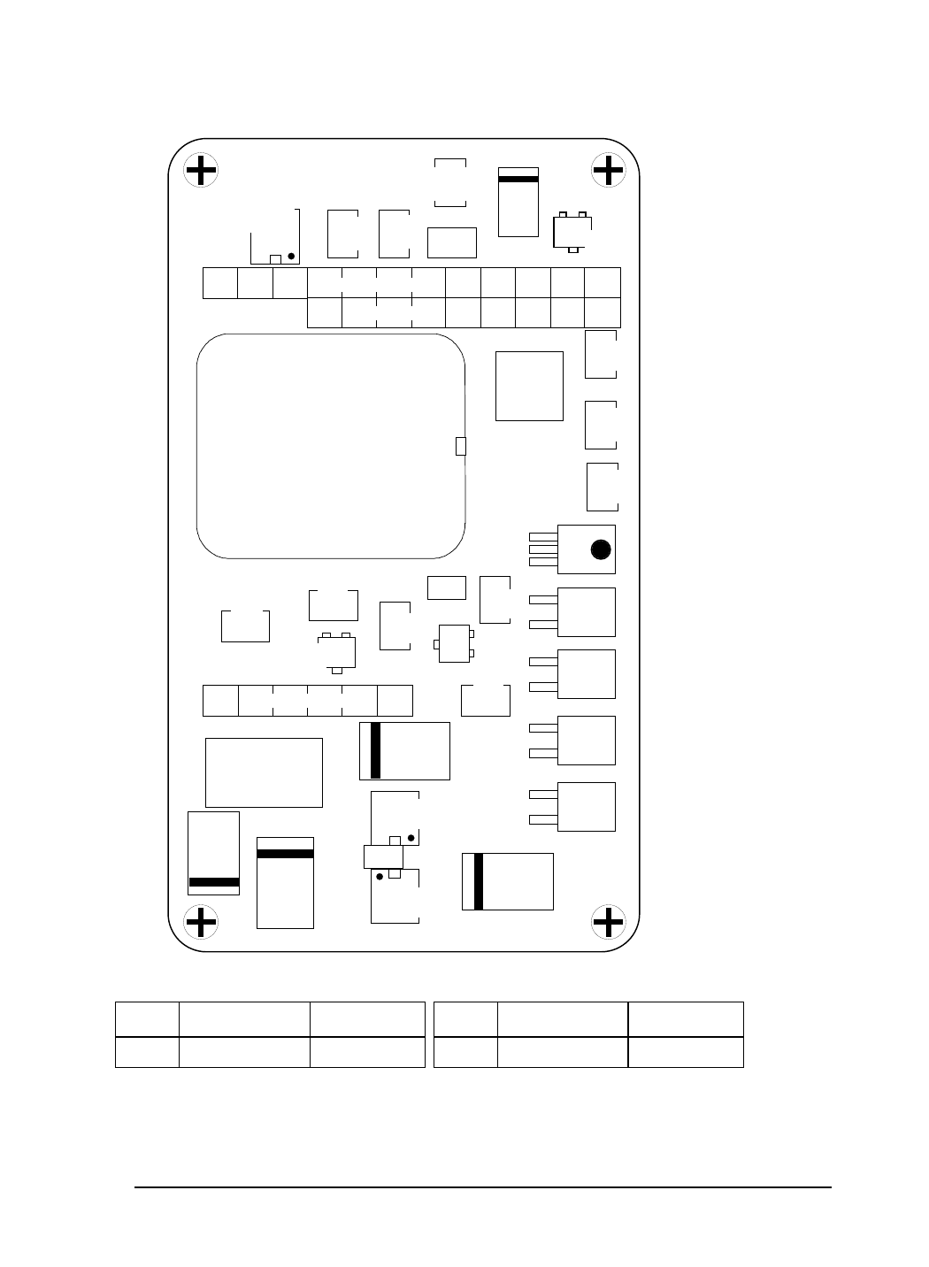
DWG No: OS3HDIGAS3A
TITLE: OS-3H DIGITAL BOARD SOLDER SIDE SM LAYOUT
DATE: 31 MARCH 1997
BOARD No.: 50021-03
REV DATE: 14 SEP 1999
DANIELS
ELECTRONICS VICTORIA, B.C.
C8
4.7uF
U3
MC33064 R8
6k81 R19
27k4
C9
100nF
Q9
BC817
U41
68HC11E2
X1
8.0Mhz
C7
22pF
R11
10M0
C6
22pF
R39
27k4
R4
27k4
R10
27k4 R25
10k0
Q2
BC817
R24
10k0
L1
10uH
C5
47uF
C3
47uF U1
SI9933Y
U2
LP2951
C4
47uF
R6
27k4
D3
BAS16
DWG No: OS3HDIGAS4B
TITLE: OS-3H DIGITAL BOARD SOLDER SIDE SM VALUE / DESIGNATION
JU2
REV DATE: 14 SEPTERMBER 1998
C15
10uF JU1
U9
OPL550
U8
OP140A
U7
OP140A
U6
OP140A
U5
OP140A
P1 1ROW x 12P
1ROW x 9P
P2 1ROW x 6P
4.5 OS(R/T)-3(A/H) Digital Board Diagrams
4.5.1 OS(R/T)-3(A/H) Digital Board Component Layout (Bottom)
DE DANIELS
ELECTRONICS
4-17
Enhanced AM/FM Synthesizer Instruction Manual OS(R/T)-3(A/H) 29 - 470 MHz
OS3150M4A
PCB 50021-03
JU2
9.6 MHz
REFERENCE 10 MHz
REFERENCE
NOT INSTALLED INSTALLED
JU1
OSx-3H
29-470 MHz OSx-3A
118-159.6 MHz
NOT INSTALLED INSTALLED
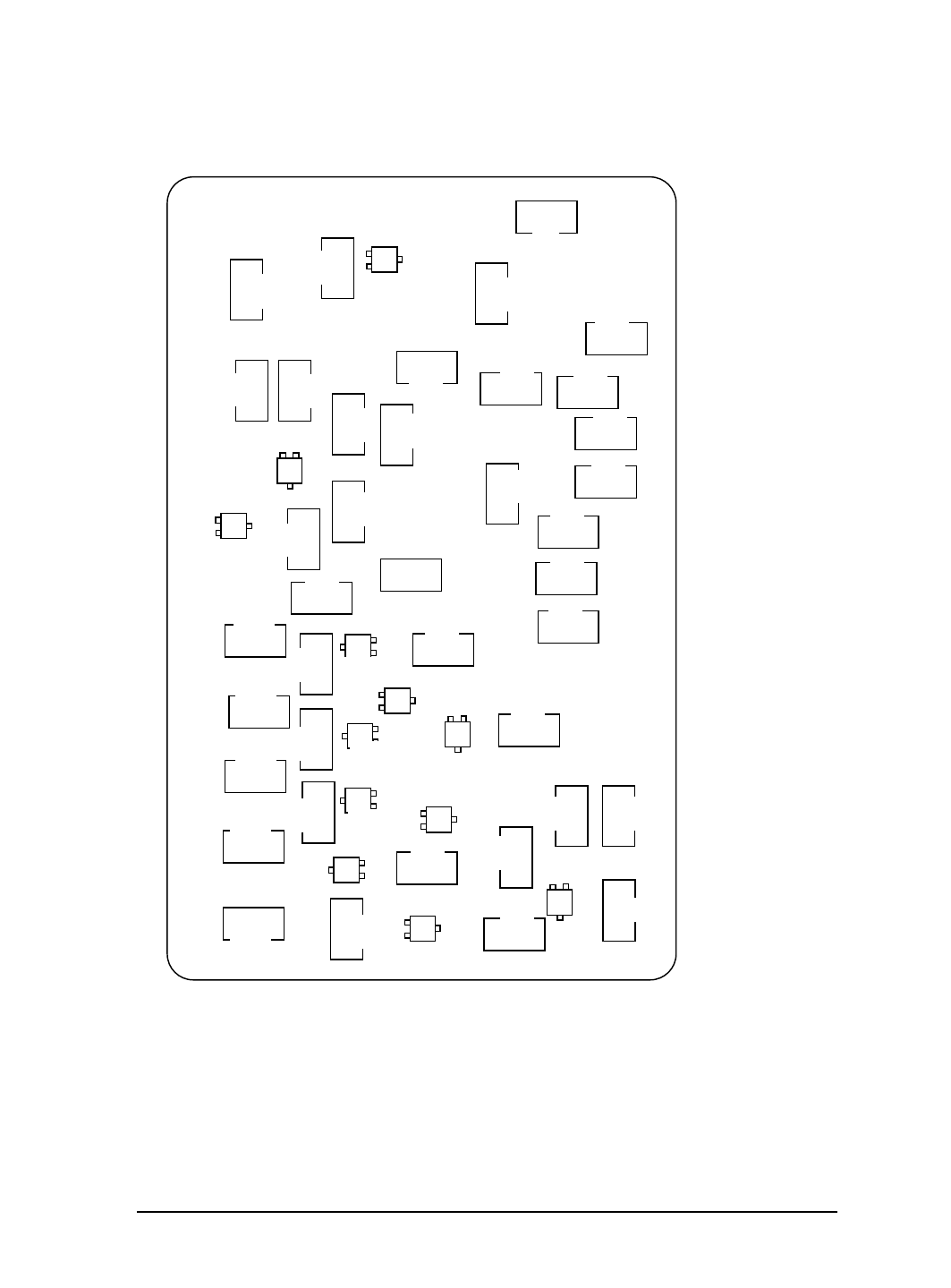
DATE: 25 MARCH 1996
DWG No: OS3HDIGAS
TITLE: OS-3H DIGITAL BOARD COMPONENT SIDE
BOARD No.: 50021-03
REV DATE: 14 SEP 99
DWG No: OS3HDIGAS1
TITLE: OS-3H DIGITAL BOARD COMPONENT SIDE SM LAYOUT
DWG No: OS3HDIGAS1A
DANIELS
ELECTRONICS VICTORIA, B.C.
R1
0R0
R20
27k4
R34
27k4 R36
27k4
R12
27k4 R18
27k4
R38
27K4
R21
27k4
R9
27k4
R7
27k4
R35
27k4
R37
27k4
R22
27k4 R5
27k4
R28
27k4
R29
27k4
R13
27k4
R14
27k4
R15
27k4
R16
27k4
R27
27k4
R26
10k0
R 17
27k4
R 33
332R
R 32
215R
R 31
215R
C10
100nF
C11
100nF
C12
100nF
C13
100nF
C14
100nF
R 30
215R
R 23
10k0
R 3
27k4
R 2
27k4 C1
100nF
C2
100nF
Q11
BC817
Q8
BC817
Q7
BC817
Q6
BC817
Q5
BC817
Q4
BC817
Q3
BC817
Q1
BC817
Q10
BC817
D1
BAS16
D2
BAS16
D4
BAS16
R40
27k4
DWG No: OS3HDIGAS2B
TITLE: OS-3H DIGITAL BOARD COMPONENT SIDE SM VALUE / DESIGNATION
R41
221k
REV DATE: 10 MAY 2000
DE DANIELS
ELECTRONICS
4-18 Enhanced AM/FM Synthesizer Instruction Manual OS(R/T)-3(A/H) 29 - 470 MHz
4.5.2 OS(R/T)-3(A/H) Digital Board Component Layout (Top)
OS3150M5B
PCB 50021-03
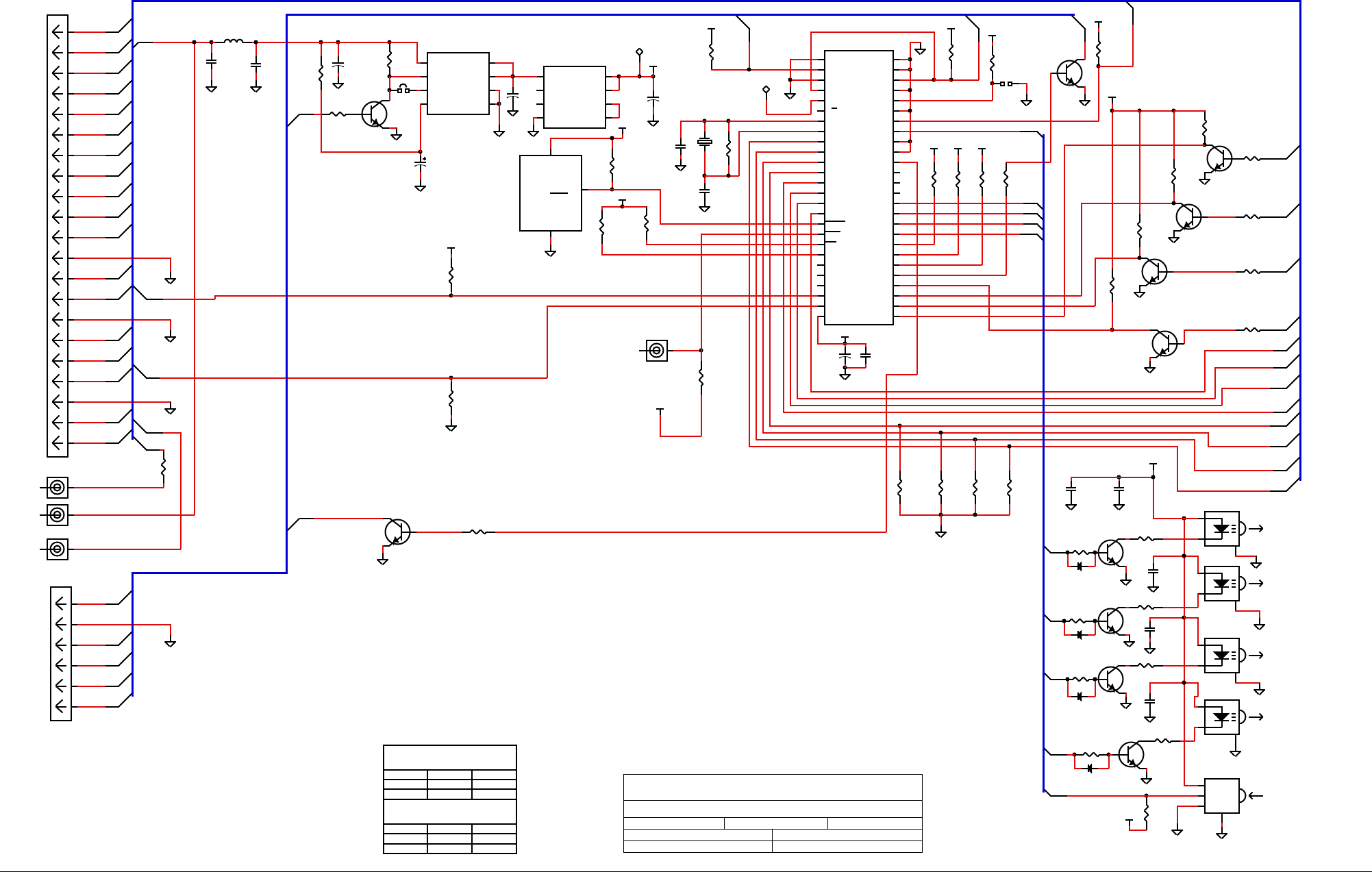
VICTORIA B.C.
DE
DANIELS
ELECTRONICS
DE
DANIELS
ELECTRONICS
DWG No: OS3150M6B DWG REV DATE: 14 APRIL 2000
4-19
4
.
5
.
3
O
S
(
R
/
T
)-
3
(
A
/
H
)
D
i
g
i
t
a
l
B
o
ard
S
c
h
e
m
a
t
i
c
D
i
a
g
ra
m
BOARD REV: 3.0
C15
R41
BOARD No: 50021-03
TITLE: OS(R/T)-3(A/H) DIGITAL BOARD SCHEMATIC DIAGRAM
Enhanced AM/FM Synthesizer Instruction Manual OS(R/T)-3(A/H) 29 - 470 MHz
J4
-----
-----
JU1
JU2
Q11 U9
X1
DWN BY: STAN P
-----
-----
-----
-----
-----
-----
UNUSED REFERENCE DESIGNATORS
APRVD:DATE: 23 APRIL 1992
----- -----
HIGHEST REFERENCE DESIGNATORS
DATA OUTPUT
+12V PRG
PRIORITY COR
LOCK DETECT INPUT
POWER CONTROL
CLK
ENABLE
ACTIVE HIGH
CHAN SEL1 (I/P)
TCXO MOD INPUT
+9.5 VDC SUPPLY
MODULATION INPUT
TCXO MOD INPUT
RX MUTE
MODULATION INPUT
POWER DOWN (I/P)
TO ALL +5 VDC SUPPLY POINTS
PC7 (I/P)
PC6 (I/P)
PC5 (I/P)
PC4 (I/P)
+9.5 VDC SUPPLY
PTT (I/P) A(L)
BOOTSTRAP (I/P)
SW4 COM (O/P)
SW3 COM (O/P)
SW2 COM (O/P)
SW1 COM (O/P)
RX DATA (I/P)
TX DATA (O/P)
PTT CONTROL (O/P)
CHAN SEL0 (I/P)
CHAN SEL2 (I/P)
CHAN SEL3 (I/P)
6K81
R8 1
2
3
BC817
Q8
BC817
Q9
BC817
Q10
27K4
R27
27K4
R34
27K4
R35
27K4
R36
BC817
Q11
27K4
R22
27K4
R37
27K4
R13
100nF
C9
BC817
Q3
27K4
R2
BC817
Q1
BC817
Q2
1
2
3
BC817
Q4
BC817
Q5
BC817
Q6
ENB
CLK
DIN
LOCK
DIN
PWCTL
OUTPUT
SENSE
5VTAP
FB
INPUT
ERROR
SHDN
GND
1
2
6
74
3
5
8
U2
LP2951
P2-2
P2-1
P2-6
P2-3
P1-1
P2-4
P1-9
P1-17
VSS
MODA
AS
E
R/W
EXTAL
XTAL
PC7
PC6
PC5
PC4
PC3
PC2
PC1
PC0
RESET
XIRQ
IRQ
PD5
PD4
PD3
PD2
PD1
PD0
VDD
MODB
VRH
PE7
PE6
PE5
PE4
PE3
PE2
PE1
PE0
PB7
PB6
PB5
PB4
PB3
PB2
PB1
PB0
PA7
PA6
PA5
PA4
PA3
PA2
PA1
PA0
VRL
1
2
3
4
5
6
7
8
16
15
14
13
12
11
10
9
17
18
19
25
24
23
22
21
20
26 34
33
32
31
30
29
28
27
42
41
40
39
38
37
36
35
43
45
47
49
44
46
48
50
51
52
68HC811E2
U4
D1
D1
D2
D2
S1
G1
S2
G2
1
2
3
4 5
6
7
8
SI9933DY
U1
P1-12
P1-19
P1-11
P1-5
P1-13
P1-6
P1-14
P1-15
P1-8
P1-16
R14
27K4 R16
27K4 27K4
R17
DGND
DGND
DGND
DGND
DGND
DGND
DGND
DGND
DGND
DGND
DGND
DGND
DGND
DGND
DGND
DGND
DGND
DGND
DGND
DGND
DGND
+5VD
+5VD
+5VD
+5VD
R15
27K4
+5VD
+5VD
+5VD
+5VD
+5VD
+5VD
DGND
+5VD
+5VD
DGND
DGND
P1-4
27K4
R5
27K4
R3
0R0
R1
27K4
R6
27K4
R4
10K0R23
10K0
R24
10K0
R25
10K0
R26
215R
R32
215R
R31
215R
R30
P1-1
P1-2
P1-4
P1-5
P1-6
P1-8
P1-9
P1-11
P1-12
P1-13
P1-14
P1-16
P1-17
P1-18
P1-19
P1-20
P1-15
C1
100nF C2
100nF
27K4
R12 27K4
R18 27K4
R19 27K4
R20
+
4.7uF
C8
+
47uF
C5
TP1
+
47uF
C4
IN
GND
RESET
1
2
4
MC33064
U3
DGND
10.0uH
L1
+
47uF
C3
DGND
P1-20
+5VD
P1-12B
1
2
3
4
5
6
P2
1J2
1
J1
1
2
3
4
5
6
7
8
9
10
11
12
13
14
15
16
17
18
19
20
21
P1
P1-12B
DGND
LOCK
CLK
ENB
R21
27K4
DGND
R29
27K4
R9
27K4
R28
27K4
27K4
R7
R10
27K4
2
1
8.0 Mhz
X1
R11
10M0
DGND
P2-1
P2-2
P2-3
P2-4
P2-6
1
J3
P1-18
C7
22pF
TP2
P1-2
DGND
DGND
R33
332R
R38
27K4
1
J4
+5VD
27K4
R39
+5VD
DGND
PWCTL
DGND
BC817
Q7
DGND
C11
100nF C10
100nF
C12
100nF
C13
100nF
C14
100nF
DGND
DGND
C6
22pF
BAS16D1
BAS16
D2
BAS16D3
BAS16D4
+5VD
27K4
R40
JU2
DGND
221K0
R41
10uF
C15
DGND
JU1
1
2
3
OP140A
U8
DGND
1
2
3
OP140A
U7
DGND
1
2
3
OP140A
U6
DGND
1
2
3
OP140A
U5
DGND
VCC
OUT
GND
1
2
3
4
U9
OPL550
DGND
P1-17

DE
DANIELS
ELECTRONICS
4-20
Enhanced AM/FM Synthesizer Instruction Manual O
S(R/T)-3(A/H) 29 - 470 MHz
This Page Intentionally Left Blank

Enhanced
AM/FM Synthesizer Instruction Manual OS(R/T)-3(A/H) 29 - 470 MHz 5-1
5.
PARTS LISTS
This is hidden text.
5.1 OS(R/T)-3H 29 - 71.4 MHz Analog Board Electrical Parts List
Ref.
Desig Description Part No.
C1
-
C3
CAP.,
SM
1.0nF
CER.,
0805,
X7R,
50V 1008-3A102K5R
C4
CAP.,
SM
10nF
CER,
0805,
X7R,
50V 1008-4A103K5R
C5
CAP.,
SM
100nF
CER.,
0805, X
7R,
50V 1008-5A104K5R
C6
CAP.,
SM
47uF TANT., 20%, 16V 1055-6D476M16
C7
CAP.,
SM
10nF
CER,
0805,
X7R,
50V 1008-4A103K5R
C8
CAP.,
SM
100nF
CER.,
0805,
X7R,
50V 1008-5A104K5R
C9
CAP.,
SM
10nF
CER,
0805,
X7R,
50V 1008-4A103K5R
C10
CAP.,
SM
100nF CER
.,
0805,
X7R,
50V 1008-5A104K5R
C11
CAP.,
SM
1.0uF
TANT., 10%, 16V 1055-5A105M16
C12
CAP.,
SM
4.7uF
TANT., 10%, 16V
1055-5B475K16
C13
CAP.,
SM
4.7uF
TANT., 10%, 16V
1055-5B475K16
C14
CAP.,
SM
10nF
CER,
0805,
X7R,
50V 1008-4A103K5R
C15
CAP.,
SM
4.7uF TANT., 10%, 16V
1055-5B475K16
C16
CAP.,
SM
1.0nF
CER.,
0805,
X7R,
50V 1008-3A102K5R
C17
CAP.,
SM
1.0nF
CER.,
0805,
X7R,
50V 1008-3A102K5R
C18
CAP.,
SM
47uF TANT., 20%, 16V 1055-6D476M16
C19
CAP.,
SM
10nF
CER,
0805,
X7R,
50V 1008-4A103K5R
C21 CA
P.,
SM
10nF
CER,
0805,
X7R,
50V 1008-4A103K5R
C20
CAP.,
SM
4.7uF
TANT., 10%, 16V
1055-5B475K16
C22
CAP.,
SM
10nF
CER,
0805,
X7R,
50V 1008-4A103K5R
C23
CAP.,
SM,
150pF
CER.,
0805,C0G 1008-2A151J1G OST-3H035
C23
CAP.,
SM,
100pF
CER.,
0805,C0G 1008-2A101J1G OST-3H045
C23
CAP.,
SM,
56pF
CER.,
0805, C0G 1008-1A560J1G OSR-3H061
C24
CAP.,
1-14pF
TRIM.,
STAND. >6 1082-A1R0014J
C25
CAP.,
SM
1.0nF
CER.,
0805,
X7R,
50V 1008-3A102K5R
C26
CAP.,
SM
1.0nF
CER.,
0805,
X7R,
50V 1008-3A102K5R
C27
CAP.,
SM
4.7uF
TANT., 10%, 16V
1055-5B475K16
C28
CAP.,
SM
1.0nF
CER.,
0805,
X7R,
50V 1008-3A102K5R
C29
CAP.,
SM
47uF TANT., 20%, 16V 1055-6D476M16
C30
CAP.,
SM
10nF
CER,
0805,
X7R,
50V 1008-4A103K5R
C31
CAP.,
SM
1.0nF
CER.,
0805,
X7R,
50V 1008-3A102K5R
C32,
C33 C
AP.,
SM,
100uF TANT., 20%,16V 1055-7D107M16
C34
CAP.,
SM,
56pF
CER.,
0805, C0G 1008-1A560J1G OST-3H035
C34
CAP.,
SM,
47pF
CER.,
0805, C0G 1008-1A470J1G OST-3H045
C34
CAP.,
SM,
33pF
CER.,
0805, C0G 1008-1A330J1G OSR-3H061
C35
CAP.,
SM
10pF
CER.,
0805, COG 1008-1A100J1G
C36
CAP.,
SM
330pF
CER.,
0805, COG 1008-2A331J1G
C37,
C38
CAP.,
1.0uF
FILM,
MMK5, 10%, 63V 1016-6D105K50
C39
CAP.,
1.0uF
FILM,
MMK5,10%,50V 1016-6D105K50
C40
CAP.,
SM
33pF
CER.,
0805, COG 1008-1A330J1G
C41
CAP.,
SM
1.0nF
CER.,
0805,
X7R,
50V 1008-3A102K5R
C42
CAP.,
22uF DIP. TANT., 20%, 20V 1054-6G226M20
C43
CAP.,
SM
10nF
CER,
0805,
X7R,
50V 1008-4A103K5R
C44
CAP.,
SM
330pF
CER.,
0805, COG 1008-2A331J1G
C45
CAP.,
470nF
FILM,
MMK5,10%,63V 1016-5D474K63
C46
CAP.,
SM
330pF
CER.
, 0805, COG 1008-2A331J1G
C47
CAP.,
SM
330pF
CER.,
0805, COG 1008-2A331J1G

5-2
Enhanced
AM/FM Synthesizer Instruction Manual OS(R/T)-3(A/H) 29 - 470 MHz
Ref.
Desig Description Part No.
C48
CAP.,
68nF
FILM,
MMK5, 10%,63V 1016-4A683K63 OST-3H035
C48
CAP.,
68nF
FILM,
MMK5, 10%,63V 1016-4A683K63 OST-3H045
C48
CAP.,
Not
Installed
Not
Installed
OSR-3H061
C49
CAP.,
22nF
FILM,
MMK5, 10%,63V 1016-4A223K63
C50
CAP.,
22uF DIP. TANT., 20%, 20V 1054-6G226M20
C51
CAP.,
SM
10nF
CER,
0805,
X7R,
50V 1008-4A103K5R
C52
CAP.,
SM
330pF
CER.,
0805, COG 1008-2A331J1G
C53
CAP.,
SM,
56pF
CER.,
0805, C0G 1008-1A560J1G OST-3H035
C53
CAP.,
SM,
56pF
CER.,
0805, C0G 1008-1A560J1G OST-3H045
C53
CAP.,
SM,
Not
Installed
Not
Installed
OSR-3H061
C54
CAP.,
22uF DIP. TANT., 20%, 20V 1054-6G226M20
C55
CAP.,
SM
10nF
CER,
0805,
X7R,
50V 1008-4A103K5R
C56 C
AP.,
SM
330pF
CER.,
0805, COG 1008-2A331J1G
C57
CAP.,
SM,
15pF
CER.,
0805, COG 1008-1A150J1G OST-3H035
C57
CAP.,
SM,
15pF
CER.,
0805, COG 1008-1A150J1G OST-3H045
C57
CAP.,
SM,
68pF
CER.,
0805, C0G 1008-1A680J1G OSR-3H061
C58
CAP.,
SM,
33pF
CER.,
0805, C0G 1008-1A330J1G OST-3H035
C58
CAP.,
SM,
33pF
CER.,
0805, C0G 1008-1A330J1G OST-3H045
C58
CAP.,
SM,
68pF
CER.,
0805, C0G 1008-1A680J1G OSR-3H061
C59
CAP.,
SM,
33pF
CER.,
0805, C0G 1008-1A330J1G OST-3H035
C59
CAP.,
SM,
33pF
CER.,
0805, C0G 1008-1A330J1G OST-3H045
C59
CAP.,
SM,
100pF
CER.,
0805,C0G 1008-2A101J1G OSR-3H061
C61
CAP.,
SM,
150pF
CER.,
0805,C0G 1008-2A151J1G OST-3H035
C61
CAP.,
SM,
100pF
CER.,
0805,C0G 1008-2A101J1G OST-3H045
C61
CAP.,
SM,
56pF
CER.,
0805, C0G 1008-1A560J1G OSR-3H061
C62 C
AP.,
SM,
47pF
CER.,
0805, C0G 1008-1A470J1G
C63
CAP.,
SM,
22pF
CER.,
0805, C0G 1008-1A220J1G
C64
CAP.,
SM,
12pF
CER.,
0805, C0G 1008-1A120J1G
D1, D2 DIODE, MMBV609L
VARICAP,
SOT-23
2106-MMBV609L
D3 DIODE, MMBD701
HOT_CARR.
SOT23 2105-MMBD7010
D4 DIODE, BYD17J
RECTIFIER,
SOD87
2101-BYD17J00
D5 DIODE, BAS16 SWITCHING, SOT23 2100-BAS16000
L1
-
L4
CHOKE,
RF/MOULD.10uH
10%,.25 1251-4A00100K
L5
INDUCTOR,13.5T/260nH,MOLD.,ORG
1253-A1352603 OST-3H035
L5 INDUCTOR,11.5T/197nH,MOLD.,BRN 1253-A1151971 OST-3H045
L5 INDUCTOR, 9.5T/138nH,MOLD.,WHT 1253-A0951389 OSR-3H061
L6 CHOKE,
RF/MOULD.10uH
10%,.25 1251-4A00100K
L7 CHOKE,
RF/MOULD.4.7uH
10%,.25
1251-TBA
L8
-
L10
CHOKE,
RF/MOULD.1.5uH
10%,.25 1251-3A001R5K
L11
INDUCTOR,SM,100nH
CER,10%,1008
1256-2BR1000K OST-3H035
L11
INDUCTOR,SM,100nH
CER,10%,1008
1256-2BR1000K OST-3H045
L11
INDUCTOR,SM,120nH
CER,10%,1008
1256-2BR12OOK
OSR-3H061
L12 CHOKE,
RF/MOULD.,4.7uH,10%,.25
1251-3A004R7K
L13
INDUCTOR,SM,100nH
CER,10%,1008
1256-2BR1000K OST-3H035
L13 INDUCTOR,SM,100nH
CER,10%,1008
1256-2BR1000K OST-3H045
L13
INDUCTOR,SM,120nH
CER,10%,1008
1256-2BR12OOK
OSR-3H061
LED1 LED, SUB-MIN., 2mm SQ,AXIAL,ORG 2012-S229013C
PCB
PCB,
ANALOG,OS-3H VHF 30-50MHz 4309-26500382

Enhanced
AM/FM Synthesizer Instruction Manual OS(R/T)-3(A/H) 29 - 470 MHz 5-3
Ref.
Desig Description Part No.
Q1, Q2 TRANSISTORBC817 NPN, SOT23 2120-BC817025
Q3 TRANSISTORBC807
PNP,
SOT23 2120-BC807025
Q4 TRANSISTORBC817 NPN, SOT23 2120-BC817025
Q5
JFET,
J211
RF
N-CHAN. TO-92 2041-J2110000
RV1
POT.,
SM
5K0 1T, TOP ADJ 1174-AS2502J1
R1
RES.,
SM
49R9 0805, 1%,100ppm 1150-1A49R9FP
R2
RES.330R
METAL
FILM,
5%, 0.5W 1101-2A0331JP
R3,
R4
RES.,
SM
10K0 0805, 1%,100ppm 1150-4A1002FP
R5
RES.,
SM
100R 0805, 1%,100ppm 1150-2A1000FP
R6
RES.,
SM
1K00 0805, 1%,100ppm 1150-3A1001FP
R7,
R8
RES.,
SM
10K0 0805, 1%,100ppm 1150-4A1002FP
R9
RES.,
SM
1K00 0805, 1%,100ppm 1150-3A1001FP
R10
-
R12
RES.,
SM
10K0 0805, 1%,100ppm 1150-4A1002FP
R13
RES.,
SM
11K8 0805, 1%,100ppm 1150-4A1182FP
R14
RES.,
SM
10K0 0805, 1%,100ppm 1150-4A1002FP
R15
RES.,
SM
10R0 0805, 1%,100ppm 1150-1A10R0FP
R16,
R17
RES.,
SM,
5K11 0805, 1%,100ppm 1150-3A5111FP
R18,
R19
RES.,
SM
10K0 0805, 1%,100ppm 1150-4A1002FP
R20
RES.,
SM
10R0 0805, 1%,100ppm 1150-1A10R0FP
R21
RES.,
SM
20K0 0805, 1%,100ppm 1150-4A2002FP
R22
RES.,
SM,
475R 0805, 1%,100ppm 1150-2A4750FP
R23
-
R25
RES.,
SM
10R0 0805, 1%,100ppm 1150-1A10R0FP
R26
RES.1R2
METAL
FILM,
5%, 0.5W 1101-0A01R2JI
R27
RES.,
SM
15K0 0805, 1%,100ppm 1150-4A1502FP
R28
RES.,
NOT INSTALLED NOT INSTALLED
R29
RES.,
SM
18K2 0805, 1%,100ppm 1150-4A1822FP
R30
RES.,
SM
10R0 0805, 1%,100ppm 1150-1A10R0FP
R31
RES.,
SM
49R9 0805, 1%,100ppm 1150-1A49R9FP
R32
RES.,
15K METAL
FILM,
5%, 0.5W 1101-4A0153JP
R33
RES.680R
METAL
FILM,
5%, 0.5W 1101-2A0681JP
R34,
R35
RES.10K0
METAL
FILM,
5%, 0.5W 1101-4A0103JP
R36 R
ES.,
2K7 METAL
FILM,
5%, 0.5W 1101-3A0272JP
R38
RES.,
SM
56R2 0805, 1%,100ppm 1150-4A5622FP
R39
RES.,
SM
0R00 0805, ZERO OHM JUMPER 1150-0A0R0000
R40
RES.180R
METAL
FILM,
5%, 0.5W 1101-2A0181JP
R41
RES.,
SM
18R2 0805, 1%,100ppm 1150-1A18R2FP
R44 RE
S.,
SM
47R5 0805, 1%,100ppm 1150-1A47R5FP
R45
RES.,
SM
27R4 0805, 1%,100ppm 1150-1A27R4FP
R46
RES.,
SM
33R2 0805, 1%,100ppm 1150-1A33R2FP
R47
RES.,
SM
47R5 0805, 1%,100ppm 1150-1A47R5FP
R48
RES.,
SM
27R4 0805, 1%,100ppm 1150-1A27R4FP
R49
RES.,
SM
33R2 0805, 1%,100ppm 1150-1A33R2FP
R50
RES.180R
METAL
FILM,
5%, 0.5W 1101-2A0181JP
R51
RES.220R
METAL
FILM,
5%, 0.5W 1101-2A0221JP
R52
RES.,
SM
49R9 0805, 1%,100ppm 1150-1A49R9FP
R53
RES.,
SM
10K0 0805, 1%,100ppm 1150-4A1002FP
R54
RES.,
SM
18R2 0805, 1%,100ppm 1150-1A18R2FP
R55 R56
RES.,
SM
274 0805, 1%,100ppm 1150-2A2740FP
TCXO1 VTCXO
MODULE9.6 MHz
4 PIN, +- 1ppm 2641-09600BM5

5-4
Enhanced
AM/FM Synthesizer Instruction Manual OS(R/T)-3(A/H) 29 - 470 MHz
Ref.
Desig Description Part No.
U1
-
U4
DIODE, OPL550 I/R
SENSOR,TTL
O/P,PLST
2014-1L18230T
U5 LED, OP140A
I/R,GaAs,.81
x
.23,PLAST.
2013-1G18230A
U6
I.C.,
LT1129-IS8,
PROG.
VOLT REG, SO8 2305-11290N08
U7, U8
I.C.,
LP2951
PROG.
VOLT REG, SO-8 2305-29510N08
U9
MOSFET,
SI9945DY, N CHAN.,SO-8 2142-SI9945DY
U10
I.C.,
MC145191,
PLL
FREQ/SYNTH,
SO-20 2355-45191N20
U11
I.C.,
MSA-0611,
MM1C
AMP,
SOT-143 2354-MSA06110
U15 U16
I.C.,
MSA-0611,
MM1C
AMP,
SOT-143 2354-MSA06110

Enhanced
AM/FM Synthesizer Instruction Manual OS(R/T)-3(A/H) 29 - 470 MHz 5-5
5.2 OS(R/T)-3A 118 - 159.4 MHz Analog Board Electrical Parts List
Ref.
Desig Description Part No.
C1- C3
CAP.,
SM
,1.0nF
CER.,
0805,
X7R,
50V 1008-3A102K5R
C4
CAP.,
SM,
10nF
CER,
0805,
X7R,
50V 1008-4A103K5R
C5
CAP.,
SM,
100nF
CER.,
0805,
X7R,
50V 1008-5A104K5R
C6
CAP.,
SM,
47uF TANT., 20%, 16V 1055-6D476M16
C7
CAP.,
SM,
10nF
CER,
0805,
X7R,
50V 1008-4A103K5R
C8
CAP.,
SM,
100nF
CER.,
0805,
X7R,
50V 1008-5A104K5R
C9
CAP.,
SM,
10nF
CER,
0805,
X7R,
50V 1008-4A103K5R
C10
CAP.,
SM,
100nF
CER.,
0805,
X7R,
50V 1008-5A104K5R
C11
CAP.,
SM,
1.0uF
TANT., 10%, 16V 1055-5A105M16
C12
CAP.,
SM,
4.7uF
TANT., 10%, 16V
1055-5B475K16
C13
CAP.,
SM,
4.7uF
TANT., 10%, 16V 1055-5B475K16
C14
CAP.,
SM,
10nF
CER,
0805,
X7R,
50V 1008-4A103K5R
C15
CAP.,
SM,
4.7uF
TANT., 10%, 16V
1055-5B475K16
C16,
C17
CAP.,
SM
,1.0nF
CER.,
0805,
X7R,
50V 1008-3A102K5R
C18
CAP.,
SM,
47uF TANT., 20%, 16V 1055-6D476M16
C19
CAP.,
SM,
10nF
CER,
0805,
X7R,
50V 1008-4A103K5R
C20
CAP.,
SM,
4.7uF
TANT., 10%, 16V
1055-5B475K16
C21,
C22
CAP.,
SM,
10nF
CER,
0805,
X7R,
50V 1008-4A103K5R
C23
CAP.,
SM,
10pF
CER.,
0805, C0G 1008-1A100J1G
(OST-3A128)
C23
CAP.,
NOT INSTALLED NOT INSTALLED (OSR-3A149)
C24
CAP.,
SM
,1.0nF
CER
.,
0805,
X7R,
50V 1008-3A102K5R
C25
CAP.,
NOT INSTALLED NOT INSTALLED
C26
CAP.,
SM
,1.0nF
CER.,
0805,
X7R,
50V 1008-3A102K5R
C27
CAP.,
SM,
4.7uF
TANT., 10%, 16V
1055-5B475K16
C28
CAP.,
SM,
6.8uF
TANT., 20%, 10V 1055-5B685M10
C29
CAP.,
SM,
47uF TANT., 20%, 16V 1055-6D476M16
C30
CAP.,
SM,
10nF
CER,
0805,
X7R,
50V 1008-4A103K5R
C31
CAP.,
SM
,1.0nF
CER.,
0805,
X7R,
50V 1008-3A102K5R
C32,
C33
CAP.,
SM,
100uF TANT., 20%,16V 1055-7D107M16
C34
CAP.,
SM,
10nF
CER,
0805,
X7R,
50V 1008-4A103K5R
C35
CAP.,
SM,
5.6pF
CE
R.,
0805, C0G 1008-0A569D1G
C36
CAP.,
SM,
3.3pF
CER.,
0805,C0G 1008-0A339J1G
C37
CAP.,
470nF
FILM,
MMK5,10%,63V 1016-5D474K63
(OST-3A128)
C37
CAP.,
1.0uF
FILM,
MMK5,10%,50V 1016-6D105K50 (OSR-3A149)
C38
CAP.,
100nF
FILM,
MMK5,10%,63V 1016-5A104K63 (OST-3A128)
C38
CAP.,
1.0uF
FILM,
MMK5,10%,50V 1016-6D105K50 (OSR-3A149)
C39
CAP.,
NOT INSTALLED NOT INSTALLED
(OST-3A128)
C39
CAP.,
1.0uF
FILM,
MMK5,10%,50V 1016-6D105K50 (OSR-3A149)
C40
CAP.,
SM,
8.2pF
CER.,
0805,C0G 1008-0A829J1G (OSR-3A149)
C40
CAP.,
NOT INSTALLED NOT INSTALLED
(OST-3A128)
C41
CAP.,
SM,
100nF
CER.,
0805,
X7R,
50V 1008-5A104K5R
C42
CAP.,
22uF DIP. TANT., 20%, 20V 1054-6G226M20
C43
CAP.,
SM,
10nF
CER,
0805,
X7R,
50V 1008-4A103K5R
C44
CAP.,
SM,
330pF
CER.,
0805, COG 1008-2A331J1G
C45
CAP.,
470nF
FILM,
MMK5,10%,63V 1016-5D474K63 (OSR-3A149)
C45
CAP.,
330nF
FILM,
MMK5,10%,50V
1016-5B334K50
(OST-3A128)
C46
CAP.,
SM,
10nF
CER,
0805,
X7R,
50V 1008-4A103K5R
C47
CAP.,
SM,
330pF
CER.,
0805, COG 1008-2A331J1G
C48
CAP.,
SM,
100nF
CER.,
0805,
X7R,
50V 1008-5A104K5R
Ref.

5-6
Enhanced
AM/FM Synthesizer Instruction Manual OS(R/T)-3(A/H) 29 - 470 MHz
Desig Description Part No.
C49
CAP.,
22nF
FILM,
MMK5, 10%,63V 1016-4A223K63 (OSR-3A149)
C49
CAP.,
2.2nF
FILM,
MMK5,10%,63V 1016-3A222K63
(OST-3A128)
C50,
C51
CAP.,
SM,
100nF
CER.,
0805,
X7R,
50V 1008-5A104K5R
C52
CAP.,
SM,
10nF
CER,
0805, X7
R,
50V 1008-4A103K5R
C53
CAP.,
SM,
27pF
CER.,
0805, COG 1008-1A270J1G
C58
CAP.,
SM,
47pF
CER.,
0805, COG 1008-1A470J1G
C59
CAP.,
SM,
27pF
CER.,
0805, COG 1008-1A270J1G
C60
CAP.,
SM,
2.2uF
TANT., 20%, 20V
1055-5B225K20
C61
CAP.,
SM,
4.7uF
TANT., 10%, 16V 10
55-5B475K16
C62
CAP.,
SM,
10nF
CER,
0805,
X7R,
50V 1008-4A103K5R
C63
CAP.,
680nF
FILM,
MMK5,10%,50V 1016-5D684K50
D1, D2 DIODE, MMBV609L
VARICAP,
SOT-23
2106-MMBV609L
D3 DIODE, MMBD701L HOT
CARR.,
SOT23 2105-MMBD7010
D4 DIODE, BYD17J
RECTIFIER,
SOD87 210
1-BYD17J00
D5 DIODE, BAS16 SWITCHING, SOT23 2100-BAS16000
D6, D7 DIODE,
SMV1211,
VARACTOR,SOT2 2106-SMV12111 (OSR-3A149)
D6 DIODE,SMV1212-4,VARACTOR,SOT23 2106-SMV12124
(OST-3A128)
D7 DIODE,
SMV1211,
VARACTOR,SOT2 2106-SMV12111 (OSR-3A149)
D7 DIODE, NOT INSTALLED NOT INSTALLED
(OST-3A128)
L2, L3 CHOKE,
RF/MOULD.,
10uH 10%,.25 1251-4A00100K
L4 CHOKE,
RF/MOULD.,
3.9uH 10%,.25 1251-3A003R9K
L5
BOBBIN
5.5
TURNS,
1.59 mm pitch 5791-A1010300
WIRE,
COPPER,
20AWG, SILVER
PLD,
10.2cm 7140-30002000(1pc 10cm, 2pcs
10mm)
L6
-
L8
CHOKE,
RF/MOULD.,
1.5uH 10%,.25 1251-3A001R5K
L11, L12 INDUCTOR,
SM,
47nH
CER,10%,1008
1256-1B47N00K
L13 CHOKE,
RF/MOULD.,
1.5uH 10%,.25 1251-3A001R5K
LED1 LED, SUB-MIN.,2mm SQ,AXIAL,ORG 2012-S229013C
PCB
PCB,
ANALOG,OS-3H AM/WB SYNTH. 4309-26500825
Q1, Q2
TRANSISTOR,
BC817 NPN, SOT23 2120-BC817025
Q3
TRANSISTOR,
BC807
PNP,
SOT23 2120-BC807025
Q4
TRANSISTOR,
BC817 NPN, SOT23 2120-BC817025
Q5
JFET,
J211
RF,
N-CHAN., TO-92A 2041-J2110000
Q6
TRANSISTOR,
MMBR901 HIGH FREQ. 2124-MMBR9010
R1 RES
.,
SM,
49R9 0805, 1%,100ppm 1150-1A49R9FP
R2
RES.,
330R METAL
FILM,
5%, 0.5W 1101-2A0331JP
R3,
R4
RES.,
SM,
10K0 0805, 1%,100ppm 1150-4A1002FP
R5
RES.,
SM,
100R 0805, 1%,100ppm 1150-2A1000FP
R6
RES.,
SM,
1K00 0805, 1%,100ppm 1150-3A1001FP
R7,
R8
RES.,
SM,
10K0 0805, 1%,100ppm 1150-4A1002FP
R9
RES.,
SM,
1K00 0805, 1%,100ppm 1150-3A1001FP
R10
-
R12
RES.,
SM,
10K0 0805, 1%,100ppm 1150-4A1002FP
R13
RES.,
SM,
11K8 0805, 1%,100ppm 1150-4A1182FP
R14
RES.,
SM,
10K0 0805, 1%,100ppm 1150-4A1002FP
R15
RES.,
SM,
10R0 0805, 1%,100ppm 1150-1A10R0FP
R16,
R17
RES.,
SM,
5K11 0805, 1%,100ppm 1150-3A5111FP
R18,
R19
RES.,
SM,
10K0 0805, 1%,100ppm 1150-4A1002FP

Enhanced
AM/FM Synthesizer Instruction Manual OS(R/T)-3(A/H) 29 - 470 MHz 5-7
Ref.
Desig Description Part No.
R20
RES.,
SM,
10R0 0805, 1%,100ppm 1150-1A10R0FP
R22
RES.,
SM,
137K0 0805, 1%,100ppm 1150-5A1373FP
R23
-
R25
RES.,
SM,
10R0 0805, 1%,100ppm 1150-1A10R0FP
R26
RES.,
1R2 METAL
FILM,
5%, 0.5W 1101-0A01R2JI
R27
RES.,
SM,
11K8 0805, 1%,100ppm 1150-4A1182FP
R28
RES.,
SM,
10R0 0805, 1%,100ppm 1150-1A10R0FP
R29
RES.,
SM,
18K2 0805, 1%,100ppm 1150-4A1822FP
R30
RES.,
SM,
10R0 0805, 1%,100ppm 1150-1A10R0FP
R31
RES.,
SM,
100R 0805, 1%,100ppm 1150-2A1000FP
R32
RES.,
15K METAL
FILM,
5%, 0.5W 1101-4A0153JP (OSR-3A149)
R32
RES.,
68K METAL
FILM,
5%, 0.5W 1101-4A0683JP
(OST-3A128)
R33
RES.,
680R METAL
FILM,
5%, 0.5W 1101-2A0681JP
R34,
R35
RES.,
SM,
10K0 0805, 1%,100ppm 1150-4A1002FP
R36
RES.,
1K8 METAL
FILM,
5%, 0.5W 1101-3A0182JP (OSR-3A149)
R36
RES.,
8K2 METAL
FILM,
5%, 0.5W 1101-3A0822JP
(OST-3A128)
R37,
R38
RES.,
SM,
49K9 0805, 1%,100ppm 1150-4A4992FP
R39
RES.,
SM,
0R00 0805, ZERO OHM JUMPER 1150-0A0R0000
R40
RES.,
330R METAL
FILM,
5%,0.5W 1101-2A0391JP
R41
RES.,
SM,
20K0 0805, 1%,100ppm 1150-4A2002FP
R42
RES.,
SM,
100K 0805, 1%,100ppm 1150-5A1003FP
R43
RES.,
SM,
137K0 0805, 1%,100ppm 1150-5A1373FP
R44
RES.
,
SM,
1K82 0805, 1%,100ppm 1150-3A1821FP
R45
RES.,
SM,
18R2 0805, 1%,100ppm 1150-1A18R2FP
R46
RES.,
SM,
475R0 0805, 1%,100ppm 1150-2A4750FP
R53
RES.,
SM,
100K 0805, 1%,100ppm 1150-5A1003FP
R57
RES.,
SM,
274K 0805, 1%, 100ppm 1150-5A2743FP
R58
RES.,
SM,
825K0 1206, 1%,100ppm 1150-5B8253FP
R59
RES.,
SM,
10K0 0805, 1%,100ppm 1150-4A1002FP
R60
RES.,
SM,
68K1 0805, 1%,100ppm 1150-4A6812FP (OSR-3A149)
R60
RES.,
SM,
39K2 0805, 1%,100ppm 1150-4A3922FP
(OST-3A128)
R61
RES.,
SM,
20K0 0805, 1%,100ppm 1150-4A2002FP
R62
RES.,
SM,
4K75 0805, 1%,100ppm 1150-3A4751FP
R63
RES.,
SM,
10R0 0805, 1%,100ppm 1150-1A10R0FP
RV1
POT.,
SM,
5K0 1T, TOP ADJ 1174-AS2502J1
TCXO1 VTCXO
MODULE9.6 MHz
4 PIN, +- 1ppm 2641-09600BM5
U1
-
U4
DIODE, OP950 I/R
SENSOR,TTL
O/P,PLST
TBA
U5 LED, OP140A
I/R,GaAs,.81
x
.23,PLAST.
2013-1G18230A
U6 IC, LT1129-IS8,
PROG.
VOLT REG,SO-8 2305-11290N08
U7, U8 IC, LP2951
PROG.
VOLT REG, SO-8 2305-29510N08
U9
MOSFET,
SI9945DY, N CHAN.,SO-8 2142-SI9945DY
U10 IC,
MC145190,PLL
FREQ/SYNTH,SO-20 2355-45190N20
U11 I
C,
MSA-0611,
MM1C
AMP,SOT-143 2354-MSA06110
U17 IC, LTC1257I 12BIT
SER.DA,S0-8
2387-12570N08
U18 IC,
PIC12C672
MICROCONTROLLER,
SO-8 TBA
U19 IC, MC33172 DUAL OP
AMP,
SO-8 2302-33172N08
U20 IC, 74HC14 HEX
SCHMITT,
SO-14 2376-00140N14

5-8
Enhanced
AM/FM Synthesizer Instruction Manual OS(R/T)-3(A/H) 29 - 470 MHz
5.3 OS(R/T)-3H 128 - 174 MHz Analog Board Electrical Parts List
Ref.
Desig Description Part No.
C1-C3
CAP.,
SM,
1.0nF
CER.,
0805,
X7R,
50V 1008-3A102K5R
C4
CAP.,
SM,
10nF
CER,
0805,
X7R,
50V 1008-4A103K5R
C5
CAP.,
SM,
100nF
CER.,
0805,
X7R,
50V 1008-5A104K5R
C6
CAP.,
SM,
47
µF
TANT., 20%, 16V 1055-6D476M16
C7
CAP.,
SM,
10nF
CER,
0805,
X7R,
50V 1008-4A103K5R
C8
CAP.,
SM,
100nF
CER.,
0805,
X7R,
50V 1008-5A104K5R
C9
CAP.,
SM,
10nF
CER,
0805,
X7R,
50V 1008-4A103K5R
C10
CAP.,
SM,
100nF
CER.,
0805,
X7R,
50V 1008-5A104K5R
C11
CAP.,
SM,
1.0µF
TANT., 10%, 16V 1055-5A105M16
C12
CAP.,
SM,
4.7µF
TANT., 10%, 16V
1055-5B475K16
C13
CAP.,
SM,
4.7µF
TANT., 10%, 16V
1055-5B475K16
C14
CAP.,
SM,
10nF
CER,
0805,
X7R,
50V 1008-4A103K5R
C15
CAP.,
SM,
4.7µF
TANT., 10%, 16V 1055-5B475K16
C16
CAP.,
SM,
1.0nF
CER.,
0805,
X7R,
50V 1008-3A102K5R
C17
CAP.,
SM
1.0nF
CER.,
0805,
X7R,
50V 1008-3A102K5R
C18
CAP.,
SM,
47µF
TANT., 20%, 16V 1055-6D476M16
C19
CAP.,
SM,
10nF
CER,
0805,
X7R,
50V 1008-4A103K5R
C20
CAP.,
SM,
4.7µF
TANT., 10%, 16V
1055-5B475K16
C21,C22
CAP.,
SM,
10nF
CER,
0805,
X7R,
50V 1008-4A103K5R
C23
CAP.,
SM,
12pF
CER.,
0805, COG 1008-1A120J1G (OS-3H141)
C23
CAP.,
SM,
6.8pF
CER.,
0805,C0G 1008-0A689J1G (OS-3H162)
C24
CAP.,
TRIM.,
1-14pF STAN. >6T 1082-A1R0014J
C25
CAP.,
SM,
1.0nF
CER.,
0805,
X7R,
50V 1008-3A102K5R (OS-3H141)
C25
CAP.,
SM,
1.0nF
CER.,
0805,
X7R,
50V 1008-3A102K5R (OS-3H162)
C26
CAP.,
SM,
1.0nF
CER.,
0805,
X7R,
50V 1008-3A102K5R
C27
CAP.,
SM,
4.7µF
TANT., 10%, 16V
1055-5B475K16
C28
CAP.,
SM,
6.
8µF
TANT., 20%, 10V 1055-5B685M10
C29
CAP.,
SM,
47µF
TANT., 20%, 16V 1055-6D476M16
C30
CAP.,
SM,
10nF
CER,
0805,
X7R,
50V 1008-4A103K5R
C31
CAP.,
SM,
1.0nF
CER.,
0805,
X7R,
50V 1008-3A102K5R
C32,
C33
CAP.,
SM,
100uF TANT., 20%,16V 1055-7D107M16
C34
CAP.,
SM,
10nF
CER,
0805,
X7R,
50V 1008-4A103K5R
C35
CAP.,
SM,
3.3pF
CER.,
0805,C0G
1008-0A339J1G (OS-3H141)
C35
CAP.,
SM,
8.2pF
CER.,
0805,C0G
1008-0A829J1G (OS-3H162)
C36
CAP.,
SM,
330pF
CER.,
0805, COG 1008-2A331J1G
C37
CAP.,
1.0µF
FILM,
MMK5, 10%, 50V 1016-6D105K50 (OS-3H141)
C37
CAP.,
1.0µF
FILM,
MMK5, 10%, 50V 1016-6D105K50 (OS-3H162)
C38
CAP.,
1.0µF
FILM,
MMK5, 10%, 50V 1016-6D105K50 (OS-3H141)
C38
CAP.,
470nF
FILM,
MMK5,10%,63V 1016-5D474K63 (OS-3H162)
C39
CAP.,
1.0µF
FILM,
MMK5, 10%, 63V 1016-6D105K50 (OS-3H141)
C39
CAP.,
NOT INSTALLED NOT INSTALLED (OS-3H162)
C40
CAP.,
SM,
12pF
CER.,
0805, C0G 1008-1A120J1G (OS-3H141)
C40
CAP.,
SM,
6.8pF
CER.,
0805,C0G 1008-0A689J1G (OS-3H162)
C42
CAP.,
22µF
DIP. TANT., 20%, 20V 1054-6G226M20
C43
CAP.,
SM,
10nF
CER,
0805,
X7R,
50V 1008-4A103K5R
C44
CAP.,
SM,
330pF
CER.,
0805, COG 1008-2A331J1G
C45
CAP.,
470nF
FILM,
MMK5,10%,63V 1016-5D474K63 (OS-3H141)
C45
CAP.,
220nF
FILM,
MMK5,10%,50V 1016-5A224K50 (OS-3H162)
C46,C47
CAP.,
SM,
330pF
CER.,
0805, COG 1008-2A331J1G
Ref.

Enhanced
AM/FM Synthesizer Instruction Manual OS(R/T)-3(A/H) 29 - 470 MHz 5-9
Desig Description Part No.
C49
CAP.,
33nF
FILM,
MMK5, 10%, 63V 1016-4A333K63 (OS-3H141)
C49
CAP.,
22nF
FILM,
MMK5, 10%, 63V 1016-4A223K63 (OS-3H162)
C50
CAP.,
22µF
DIP. TANT., 20%, 20V 1054-6G226M20
C51
CAP.,
SM,
10nF
CER,
0805,
X7R,
50V 1008-4A103K5R
C52
CAP.,
SM,
330pF
CER.,
0805, COG 1008-2A331J1G
C53
CAP.,
SM,
27pF
CER.,
0805, COG 1008-1A270J1G
C54
CAP.,
22µF
DIP. TANT., 20%, 20V 1054-6G226M20
C55
CAP.,
SM,
10nF
CER,
0805,
X7R,
50V 1008-4A103K5R
C56
CAP.,
SM,
330pF
CER.,
0805, COG 1008-2A331J1G
C58
CAP.,
SM,
47pF
CER.,
0805, COG 1008-1A470J1G
C59
CAP.,
SM,
27pF
CER.,
0805, COG 1008-1A270J1G
D1 DIODE, NOT INSTALLED NOT INSTALLED
D2 DIODE, MMBV609L
VARICAP,
SOT-23
2106-MMBV609L
D3 DIODE, MMBD701L HOT
CARR.,
SOT23 2105-MMBD7010
D4 DIODE, BYD17J
RECTIFIER,SOD87
2101-BYD17J00
D5 DIODE, BAS16 SWITCHING, SOT23 2100-BAS16000
L1-L3 CHOKE,
RF/MOULD.,
10uH
10%,.25
1251-4A00100K
L4 CHOKE,
RF/MOULD.,
1.5uH
10%,.25
1251-3A001R5K
L5
BOBBIN,
5.5
TURNS,
1.59 mm pitch 5791-A1010300
WIRE,
COPPER,
20AWG, Ag PLATED, 11cm 7140-30002000(1pc 9cm, 2pcs
1cm)
L6-L10 CHOKE,
RF/MOULD.,
1.5uH
10%,.25
1251-3A001R5K
L11,L12 INDUCTOR,
SM,
47nH
CER,10%,1008
1256-1B47N00K
L12 INDUCTOR,
SM,
47nH
CER,10%,1008
1256-1B47N00K
LED1 LED, SUB-MIN.,2mm SQ,AXIAL,ORG 2012-S229013C
PCB
PCB,
ANALOG, OS-3H H/P SYNTH. 4309-26500252
Q1,Q2
TRANSISTOR,
BC817-25,NPN,SOT23 2120-BC817025
Q3
TRANSISTOR,
BC807
PNP,
SOT23 2120-BC807025
Q4
TRANSISTOR,
BC817 NPN, SOT23 2120-BC817025
Q5 JFET, J211
RF,
N-CHAN., TO-92A 2041-J2110000
R1
RES.,
SM,
49R9 0805, 1%,100ppm 1150-1A49R9FP
R2
RES.,
330R METAL
FILM,
5%, 0.5W 1101-2A0331JP
R3,R4
RES.,
SM,
10K0 0805, 1%,100ppm 1150-4A1002FP
R5
RES.,
SM,
100R 0805, 1%,100ppm 1150-2A1000FP
R6
RES.,
SM,
1K00 0805, 1%,100ppm 1150-3A1001FP
R7,R8
RES.,
SM,
10K0 0805, 1%,100ppm 1150-4A1002FP
R9
RES.,
SM,
1K00 0805, 1%,100ppm 1150-3A1001FP
R10-R12
RES.,
SM,
10K0 0805, 1%,100ppm 1150-4A1002FP
R13
RES.,
SM,
11K8 0805, 1%,100ppm 1150-4A1182FP
R14 R
ES.,
SM,
10K0 0805, 1%,100ppm 1150-4A1002FP
R15
RES.,
SM,
10R0 0805, 1%,100ppm 1150-1A10R0FP
R16,
R17
RES.,
SM,
5K11 0805, 1%,100ppm 1150-3A5111FP
R18,
R19
RES.,
SM,
10K0 0805, 1%,100ppm 1150-4A1002FP
R20
RES.,
SM,
10R0 0805, 1%,100ppm 1150-1A10R0FP
R21
RES.,
SM,
20K0 0805, 1%,100ppm 1150-4A2002FP
R22
RES.,
SM,
ZERO OHM
JUMPER,0805
1150-0A0R0000 (OSR-3H1xx)
R22
RES.,
SM,
100R 0805, 1%,100ppm 1150-2A1000FP
(OST-3H1xx)

5-10
Enhanced
AM/FM Synthesizer Instruction Manual OS(R/T)-3(A/H) 29 - 470 MHz
Ref.
Desig Description Part No.
R23-R25
RES.,
SM,
10R0 0805, 1%,100ppm 1150-1A10R0FP
R26
RES.,
1R2 METAL
FILM,
5%, 0.5W 1101-0A01R2JI
R27
RES.,
SM,
11K8 0805, 1%,100ppm 1150-4A1182FP
R28
RES.,
NOT INSTALLED NOT INSTALLED
R29
RES.,
SM,
3K92 0805, 1%,100ppm 1150-3A3921FP
R30
RES.,
SM,
10R0 0805, 1%,100ppm 1150-1A10R0FP
R31
RES.,
SM,
49R9 0805, 1%,100ppm 1150-1A49R9FP
R32
RES.,
12K METAL
FILM,
5%, 0.5W 1101-4A0123JP (OS-3H141)
R32
RES.,
15K METAL
FILM,
5%, 0.5W 1101-4A0153JP (OS-3H162)
R33
RES.,
680R METAL
FILM,
5%, 0.5W 1101-2A0681JP
R34,R35
RES.,
SM,
10K0 0805, 1%,100ppm 1150-4A1002FP
R36
RES.,
2K2 METAL
FILM,
5%, 0.5W 1101-3A0222JP (OS-3H141)
R36
RES.,
6K2 METAL
FILM,
5%, 0.5W 1101-3A0622JP (OS-3H162)
R39
RES.,
SM,
0 0805, ZERO OHM
JUMPER
1150-0A0R0000
R40
RES.,
180R METAL
FILM,
5%, 0.5W 1101-2A0181JP
R41
RES.,
S
M,
18R2 0805, 1%,100ppm 1150-1A18R2FP
R44
RES.,
SM,
47R5 0805, 1%,100ppm 1150-1A47R5FP
R45
RES.,
SM,
27R4 0805, 1%,100ppm 1150-1A27R4FP
R46
RES.,
SM,
33R2 0805, 1%,100ppm 1150-1A33R2FP
R47,
R48
RES.,
SM,
47R5 0805, 1%,100ppm 1150-1A47R5FP
R49 RES
.,
SM,
10R0 0805, 1%,100ppm 1150-1A10R0FP
R50
RES.,
180R METAL
FILM,
5%, 0.5W 1101-2A0181JP
R51
RES.,
NOT INSTALLED NOT INSTALLED
R52
RES.,
SM,
49R9 0805, 1%,100ppm 1150-1A49R9FP
R53
RES.,
SM,
10K0 0805, 1%,100ppm 1150-4A1002FP
R54
RES.,
SM,
18R2 0805, 1%,100ppm 1150-1A18R2FP
R55
RES.,
SM,
274 0805, 1%,100ppm 1150-2A2740FP
R56
RES.,
SM,
274 0805, 1%,100ppm 1150-2A2740FP
RV1
POT.,
SM,
5K0 1T, TOP ADJ 1174-AS2502J1
TCXO1 VTCXO MODULE,
9.6 MHz
4 PIN, +- 1ppm 2641-09600BM5
U1-U4 DIODE, I/R
SENSOR,TTL
O/P,PLST
2014-1L18230T
U5 LED,
I/R,GaAs,.81
x
.23,PLAST.
2013-1G18230A
U6
I.C.,
LT1129-IS8
,PROG.
VOLT
REG,SO8
2305-11290N08
U7,U8
I.C.,
LP2951
PROG.
VOLT REG, SO-8 2305-29510N08
U9
MOSFET,
SI9945DY, N
CHAN.,SO-8
2142-SI9945DY
U10 IC, 4
5193,PLL
FREQ/SYNTH,SO-20 2355-45193N20
U11 IC, MSA-0611,
MM1C
AMP,SOT-143 2354-MSA06110
U15,U16 IC, MSA-0611,
MM1C
AMP,SOT-143 2354-MSA06110

Enhanced
AM/FM Synthesizer Instruction Manual OS(R/T)-3(A/H) 29 - 470 MHz 5-11
5.4 OS(R/T)-3H 406 - 470 MHz Analog Board Electrical Parts List
Ref.
Desig Description Part No.
C1
-
C3
CAP.,
SM
1.0nF
CER.,
0805,
X7R,
50V 1008-3A102K5R
C4
CAP.,
SM
10nF
CER,
0805,
X7R,
50V 1008-4A103K5R
C5
CAP.,
SM
100nF
CER.,
0805,
X7R,
50V 1008-5A104K5R
C6
CAP.,
SM
47uF TANT., 20%, 16V 1055-6D476M16
C7
CAP.,
SM
10nF
CER,
0805,
X7R,
50V 1008-4A103K5R
C8
CAP.,
SM
100nF
CER.,
0805,
X7R,
50V 1008-5A104K5R
C9
CAP.,
SM
10nF
CER,
0805,
X7R,
50V 1008-4A103K5R
C10
CAP.,
SM
100nF
CER.,
0805,
X7R,
50V 1008-5A104K5R
C11
CAP.,
SM
1.0uF
TANT., 10%, 16V 1055-5A105M16
C12,
C13
CAP.,
SM
4.7uF
TANT., 10%, 16V 10
55-5B475K16
C14
CAP.,
SM
10nF
CER,
0805,
X7R,
50V 1008-4A103K5R
C15
CAP.,
SM
4.7uF
TANT., 10%, 16V
1055-5B475K16
C16
CAP.,
100nF
FILM,
MMK5, 10%, 63V 1016-5A104K63
C17
CAP.,
SM
1.0nF
CER.,
0805,
X7R,
50V 1008-3A102K5R
C18
CAP.,
SM
47uF TANT., 20%, 16V 1055-6D476M16
C19
CAP.,
SM
10nF
CER,
0805,
X7R,
50V 1008-4A103K5R
C20
CAP.,
SM
4.7uF
TANT., 10%, 16V
1055-5B475K16
C21,
C22
CAP.,
SM
10nF
CER,
0805,
X7R,
50V 1008-4A103K5R
C25,
C26
CAP.,
SM
1.0nF
CER.,
0805,
X7R,
50V 1008-3A102K5R
C27
CAP.,
SM
4.7uF
TANT., 10%, 16V
1055-5B475K16
C29
CAP.,
SM
47uF TANT., 20%, 16V 1055-6D476M16
C30
CAP.,
SM
10nF
CER,
0805,
X7R,
50V 1008-4A103K5R
C31
CAP.,
SM
1.0nF
CER.,
0805,
X7R,
50V 1008-3A102K5R
C32,
C33
CAP.,
SM,
100uF TANT., 20%,16V 1055-7D107M16
C34
CAP.,
SM
10nF
CER,
0805,
X7R,
50V 1008-4A103K5R
C35
CAP.,
SM
100pF
CER.,
0805, COG 1008-2A101J1G
C36
CAP.,
SM
330pF
CER.,
0805, COG 1008-2A331J1G
C37
CAP.,
1.0uF
FILM,
MMK5,10%,50V 1016-6D105K50
C38
CAP.,
NOT INSTALLED NOT INSTALLED OST-3H4xx
C38 C
AP.,
1.0uF
FILM,
MMK5,10%,50V 1016-6D105K50 OSR-3H440
C39
CAP.,
NOT INSTALLED NOT INSTALLED OST-3H4xx
C39
CAP.,
1.0uF
FILM,
MMK5,10%,50V 1016-6D105K50 OSR-3H440
C42
CAP.,
22uF DIP. TANT., 20%, 20V 1054-6G226M20
C43
CAP.,
SM
10nF
CER,
0805,
X7R,
50V 1008-4A103K5R
C44
CAP.,
SM
330pF
CER.,
0805, COG 1008-2A331J1G
C45
CAP.,
220nF
FILM,
MMK5,10%,50V 1016-5A224K50 OST-3H4xx
C45
CAP.,
470nF
FILM,
MMK5,10%,50V 1016-5C474K50 OSR-3H440
C46
CAP.,
SM
330pF
CER.,
0805, COG 1008-2A331J1G
C47
CAP.,
SM
330pF CER
.,
0805, COG 1008-2A331J1G
C49
CAP.,
22nF
FILM,
MMK5, 10%,63V 1016-4A223K63 OST-3H4xx
C49
CAP.,
33nF
FILM,
MMK5, 10%,63V 1016-4A333K63 OSR-3H440
C50
CAP.,
22uF DIP. TANT., 20%, 20V 1054-6G226M20
C51
CAP.,
SM
10nF
CER,
0805,
X7R,
50V 1008-4A103K5R
C52
CAP.,
SM
330pF
CER.,
0805, COG 1008-2A331J1G
C53
CAP.,
SM,
10pF
CER.,
0805, C0G 1008-1A100J1G
C54
CAP.,
22uF DIP. TANT., 20%, 20V 1054-6G226M20
C55
CAP.,
SM
10nF
CER,
0805,
X7R,
50V 1008-4A103K5R
C56
CAP.,
SM
330pF
CER.,
0805, COG 1008-2A331J1G
C58
CAP.,
SM,
15pF
CER.,
0805, C0G 1008-1A150J1G
Ref.

5-12
Enhanced
AM/FM Synthesizer Instruction Manual OS(R/T)-3(A/H) 29 - 470 MHz
Desig Description Part No.
C59
CAP.,
SM,
10pF
CER.,
0805, C0G 1008-1A100J1G
C60
CAP.,
100nF
FILM,
MMK5, 10%, 63V 1016-5A104K63 OST-3H4xx
C60
CAP.,
NOT INSTALLED NOT INSTALLED OSR-3H440
D4 DIODE, BYD17J RECTIFIER,SOD87
2101-BYD17J00
D5 DIODE, BAS16 SWITCHING, SOT23 2100-BAS16000
L1
-
L3 CHOKE,
RF/MOULD.10uH
10%,.25 1251-4A00100K
L6
-
L10
CHOKE,
RF/MOULD.1.5uH
10%,.25 1251-3A001R5K
L11 L12 INDUCTOR, SM18nH
CER,10%,1008
1256-1B18N00K
LED1 LED, SUB-MIN.,2mm SQ,AXIAL,ORG 2012-S229013C
PCB
PCB,
ANALOG, OS-3H UHF SYNTH. 4309-27500282
Q1, Q2
TRANSISTOR,
BC817 NPN, SOT23 2120-BC817025
Q3
TRANSISTOR,
BC807
PNP,
SOT23 2120-BC807025
Q4
TRANSISTOR,
BC817 NPN, SOT23 2120-BC817025
R1
RES.,
SM
49R9 0805, 1%,100ppm 1150-1A49R9FP
R2
RES.330R
METAL
FILM,
5%, 0.5W 1101-2A0331JP
R3 R4
RES.,
SM
10K0 0805, 1%,100ppm 1150-4A1002FP
R5
RES.,
SM
100R 0805, 1%,100ppm 1150-2A1000FP
R6
RES.,
SM
1K00 0805, 1%,100ppm 1150-3A1001FP
R7 R8
RES.,
SM
10K0 0805, 1%,100ppm 1150-4A1002FP
R9
RES.,
SM
1K00 0805, 1%,100ppm 1150-3A1001FP
R10
-
R12
RES.,
SM
10K0 0805, 1%,100ppm 1150-4A1002FP
R13
RES.,
SM
11K8 0805, 1%,100ppm 1150-4A1182FP
R14
RES.,
SM
10K0 0805, 1%,100ppm 1150-4A1002FP
R15
RES.,
SM
10R0 0805, 1%,100ppm 1150-1A10R0FP
R16,
R17
RES.,
SM,
5K11 0805, 1%,100ppm 1150-3A5111FP
R18,
R19
RES.,
SM
10K0 0805, 1%,100ppm 1150-4A1002FP
R21
RES.,
2K7 METAL
FILM,
5%, 0.5W 1101-3A0272JP OST-3H4xx
R21
RES.,
NOT INSTALLED NOT INSTALLED OSR-3H440
R23
RES.,
SM
10R0 0805, 1%,100ppm 1150-1A10R0FP
R24,
R25
RES.,
SM
10R0 0805, 1%,100ppm 1150-1A10R0FP
R26
RES.1R2
METAL
FILM,
5%, 0.5W 1101-0A01R2JI
R28 NOT INSTALLED NOT INSTALLED OST-3H418
R28
RES.,
SM
10R0 0805, 1%,100ppm 1150-1A10R0FP OSR-3H440
R28
RES.,
SM
10R0 0805, 1%,100ppm 1150-1A10R0FP OST-3H460
R29
RES.,
SM
3K92 0805, 1%,100ppm 1150-3A3921FP OST-3H418
R29
RES.,
SM
36K5 0805, 1%,100ppm 1150-4A3652FP OSR-3H440
R29
RES.,
SM
36K5 0805, 1%,100ppm 1150-4A3652FP OST-3H460
R30
RES.,
SM
10R0 0805, 1%,100ppm 1150-1A10R0FP
R31
RES.,
SM
274R 0805, 1%,100ppm 1150-2A2740FP
R32
RES.,
4K7 METAL
FILM,
5%, 0.5W 1101-3A0472JP OSR-3H440
R32
RES.,
5K6 METAL
FILM,
5%, 0.5W 1101-3A0562JP OST-3H4xx
R33
RES.680R
METAL
FILM,
5%, 0.5W 1101-2A0681JP
R34,
R35
RES.,
SM
10K0 0805, 1%,100ppm 1150-4A1002FP
R36
RES.,
2K2 METAL
FILM,
5%, 0.5W 1101-3A0222JP OST-3H4xx
R36
RES.,
1K5 METAL
FILM,
5%, 0.5W 1101-3A0152JP OSR-3H440
R39
RES.,
SM
0R0 0805, ZERO OHM JUMPER 1150-0A0R0000
Ref.

Enhanced
AM/FM Synthesizer Instruction Manual OS(R/T)-3(A/H) 29 - 470 MHz 5-13
Desig Description Part No.
R40
RES.180R
METAL FILM, 5%, 0.5W 1101-2A0181JP
R41
RES.,
SM
18R2 0805, 1%,100ppm 1150-1A18R2FP
R44
RES.,
SM
47R5 0805, 1%,100ppm 1150-1A47R5FP
R45
RES.,
SM
27R4 0805, 1%,100ppm 1150-1A27R4FP
R46
RES.,
SM
33R2 0805, 1%,100ppm 1150-1A33R2FP
R47
RES.,
SM
47R5 0805, 1%,100ppm 1150-1A47R5FP
R48
RES.,
SM
47R5 0805, 1%,100ppm 1150-1A47R5FP OST-3H418
R48
RES.,
SM
27R4 0805, 1%,100ppm 1150-1A27R4FP OSR-3H440
R48
RES.,
SM
27R4 0805, 1%,100ppm 1150-1A27R4FP OST-3H460
R49
RES.,
SM
10R0 0805, 1%,100ppm 1150-1A10R0FP OST-3H418
R49 RE
S.,
SM
33R2 0805, 1%,100ppm 1150-1A33R2FP OSR-3H440
R49
RES.,
SM
33R2 0805, 1%,100ppm 1150-1A33R2FP OST-3H460
R50
RES.180R
METAL
FILM,
5%, 0.5W 1101-2A0181JP
R51
RES.220R
METAL
FILM,
5%, 0.5W 1101-2A0221JP
R52 NOT INSTALLED NOT INSTALLED OST-3H418
R52 RE
S.,
SM
49R9 0805, 1%,100ppm 1150-1A49R9FP OSR-3H440
R52
RES.,
SM
49R9 0805, 1%,100ppm 1150-1A49R9FP OST-3H460
R53
RES.,
SM
10K0 0805, 1%,100ppm 1150-4A1002FP
R54
RES.,
SM
18R2 0805, 1%,100ppm 1150-1A18R2FP
R55,
R56
RES.,
SM
274R 0805, 1%,100ppm 1150-2A2740FP
R57
RES.,
SM
18R2 0805, 1%,100ppm 1150-1A18R2FP
R58
RES.,
SM
274R 0805, 1%,100ppm 1150-2A2740FP
RV1
POT.,
SM5K0 1T, TOP ADJ 1174-AS2502J1
TCXO1 VTCXO MODULE
9.6 MHz
4 PIN, +- 1ppm 2641-09600BM5
U1
-
U4 DIODE, OPL550 I/R
SENSOR,TTL
O/P,PLS
T 2014-1L18230T
U5 LED, OP140A
I/R,GaAs,.81
x
.23,PLAST.
2013-1G18230A
U6
I.C.,
LT1129-IS8,PROG.
VOLT REG, SO8 2305-11290N08
U7, U8
I.C.LP2951
PROG.
VOLT REG, SO-8 2305-29510N08
U9
MOSFET,
SI9945DY, N CHAN.,SO-8 2142-SI9945DY
U10
I.C.,
MC145193,
PLL FREQ/SYNTH, SO-20 2355-45193N20 OST-3H418
U10
I.C.,
MC145190,
PLL
FREQ/SYNTH,
SO-20 2355-45190N20 OSR-3H440
U10
I.C.,
MC145190,
PLL
FREQ/SYNTH,
SO-20 2355-45190N20 OST-3H460
U11
I.C.,
MSA-0611,
MM1C
AMP,
SOT-143 2354-MSA06110
U15, U16
I.C.,
MSA-0611,
MM1C
AMP,
SOT-143 2354-MSA06110
U17 VCO MODULE,427.4-451.4MHz,T-PK 2621-L002309T OSR-3H440
U17 VCO MODULE,
406-470 MHz,T-PKG.
2621-190435MT OST-3H4xx

5-14
Enhanced
AM/FM Synthesizer Instruction Manual OS(R/T)-3(A/H) 29 - 470 MHz
5.5 OS(R/T)-3(A/H)
Digital Board Electrical Parts List
Ref.
Desig Description Part No.
C1,C2
CAP.,
SM,
100nF
CER.,
0805,
X7R,
50V 1008-5A104K5R
C3-C5
CAP.,
SM,
47µF
TANT., 20%, 16V 1055-6D476M16
C6,C7
CAP.,
SM,
22pF
CER.,
0805, COG 1008-1A220J1G
C8
CAP.,
SM,
4.7µF
TANT., 10%, 16V
1055-5B475K16
C9-C14
CAP.,
SM,
100nF
CER.,
0805,
X7R,
50V 1008-5A104K5R
C15
CAP.,
SM,
10µF
TANT., 20%, 16V 1055-6C106M16
P1 INTERCONNECT/STD,1ROW x
12P,Au
5015-IS112G21
INTERCONNECT/STD,1ROW x9PIN,Au 5015-IS109G21
P2 INTERCONNECT/STD,1ROW x6PIN,Au 5015-IS106G21
D1
-
D4
DIODE, BAS16 SWITCHING, SOT23 2100-BAS16000
L1 INDUCTOR,
SM,
10.0uH,
10%,1812 1255-4G10000K
PCB
PCB,
DIGITAL, OS-3H H/P SYNTH. 4309-26500213
Q1
-
Q11
TRANSISTOR,
BC817-25,NPN,SOT23 2120-BC817025
R1
RES.,
SM,
0 0805, ZERO OHM
JUMPER
1150-0A0R0000
R2-R7
RES.,
SM,
47K5 0805, 1%,100ppm 1150-4A4752FP
R8
RES.,
SM,
6K81 0805, 1%,100ppm 1150-3A6811FP
R9,R10
RES.,
SM,
47K5 0805, 1%,100ppm 1150-4A4752FP
R11
RES.,
SM,
10M0 1206, 5%,400ppm
1151-7B0106JG
R12-R22
RES.,
SM,
47K5 0805, 1%,100ppm 1150-4A4752FP
R23-R26
RES.,
SM,
10K0 0805, 1%,100ppm 1150-4A1002FP
R27-R29
RES.,
SM,
47K5 0805, 1%,100ppm 1150-4A4752FP
R30-R32
RES.,
SM,
215R 0805, 1%,100ppm 1150-2A2150FP
R33
RES.,
SM,
332R 0805, 1%,100ppm 1150-2A3320FP
R34-R40
RES.,
SM,
47K5 0805, 1%,100ppm 1150-4A4752FP
R41
RES.,
SM,
221K 0805, 1%, 100ppm 1150-5A2213FP
U1
MOSFET,
SI9933DY, P
CHAN.,SO-8
2142-SI9933DY
U2 IC,
LP2951,PROG.
VOLT REG,SO-8 2305-29510N08
U3 IC, MC33064,UNDR/VOLT SEN.SO-8 2308-33064N08
U4 IC, 68HC811E2,
MIC/CTR,
PLCC52 2380-68811P52
U5-U8 LED,
I/R,GaAs,.81
x
.23,PLAS
T. 2013-1G18230A
U9 DIODE, I/R
SENSOR,TTL
O/P,PLST
2014-1L18230T
X1 RESONATOR,
SM,
8.0MHz, CERAMIC 1575-8001816A

Enhanced
AM/FM Synthesizer Instruction Manual OS(R/T)-3(A/H) 29 - 470 MHz 5-15
5.6 OS(R/T)-3(A/H)
Synthesizer Mechanical Parts List
Description Part No. Qty.
CASE,
OS-3H SYNTH. MODULE,ALUM 3702-66100920 1
CONN.,
SMB, JACK,2 HOLE FLANGE 5120-J2SC01BG 2
FERRITE,
BEAD,73 MIX,
3X3.5mm
OD
(CON3-CON5)
1210-73030350 3 OS-3H050
FERRITE,
BEAD,43 MIX,
3X3.5mm
OD
(CON3-CON5)
1210-43030350 3 OS-3A130
FERRITE,
BEAD,43 MIX,
3X3.5mm
OD
(CON3-CON5)
1210-43030350 3 OS-3H150
FERRITE,
BEAD,61 MIX,
3X3.5mm
OD
(CON3-CON5)
1210-61030350 3 OS-3H440
HEADER,
.1”,
1 ROWX3PIN, AU 5010-H103ST7L 2
LABEL,
FOIL,FRQ/SN,OS-3H
SYNTH 3501-13091006 1
LID,
CASE,OS-3H
SYNTH/MODL.,AL 3702-66100921 1
PIN, 2 x
10mm,
GROOVED W/PILOT 5876-D1470210 4
SCREW,
M2.0
x 4, FLAT/PHIL, A2
5812-2M0FP04S
8
SCREW,
M2 X 4, PAN/PHILLIPS,A2
5812-2M0PP04S
15
SCREW,
M2.5
x 24.5 FLAT/PHIL, A2
5812-2M5FP24S
1
WASHER,
TFE,0.036ID,1/8OD,.02T
5805-T3612F20 6

5-16
Enhanced
AM/FM Synthesizer Instruction Manual OS(R/T)-3(A/H) 29 - 470 MHz
This Page Intentionally Left Blank

Enhanced
AM/FM Synthesizer Instruction Manual OS(R/T)-3(A/H) 29 - 470 MHz 7-1
6.
REVISION HISTORY
ISSUE DATE REVISION
1 May 97 • Issue 1
2 Mar 98 • Changes to the AM
Analog
board (OST-3A128) to
improve
performance
ECO #547.
C37 was 220nF is now 100nF and C40 was 8.2pF is now not
installed
C45 was 33nF is now 22nF and C49 was 2.2nF is now 1.5nF
R32 was 33kΩ is now 56kΩand R36 was 3k3Ω is now 5k6Ω
3 Mar 00 • Changes to the AM
Analog
board to
improve
performance
at -40˚C.
ECO #565.
L4 was
1.5µH
is now 3.9
µH
• Changes to the FM
Analog
boards to
improve
manufacturing.
ECO #572
C32 & C33
were
1
00µF
through hole
tantalums
are now
100µF
surface mount
tantalums
• Changes to the OS-3A/H
Digital
board for
compatibility
with
the new AM
wideband
Synthesizers. ECO #579.
Added C15
(10µF)
and R41 (221kΩ).
JU1 was added and is
installed
for AM modules only.
PCB,
DIGITAL,
OS-3H/P SYNTH was
version
2 now
version
3.
• Added the new
component
layouts,
schematic
diagram
and parts lists for the new
AM
wideband
synthesizer. Wideband referring to only
having
to be tune
once and working
over
the
whol
e AM band (118-138 MHz).
4 May 00 • Changes to the
OS-3H
128-174 MHz
Analog
board. ECO #603.
R29 was 18k2 is now 3k92, U10 was MC145191 is now MC145193.
• Changes to the OSR-3H 128-174 MHz
Analog
board. ECO #609.
R22 was 100R is now 0R0.
• Changes to the OS-3A 118-159.4
Analog
board. ECO #601.
R42 & r53
were
137kΩ are now 100kΩ.
Jul 00 •
Corrected
the
SELECT
table
on the OS(R/T)-3H 128-174 MHz
Schematic
diagram
(section 4.3.3).

7-2
Enhanced
AM/FM Synthesizer Instruction Manual OS(R/T)-3(A/H) 29 - 470 MHz
ISSUE DATE REVISION
4 Aug 00 • Changes to the OS(R/T)-3(A/H)
Digital
board. ECO #599.
R30,
R31 & R32
were
332R are now 215R.
• Changes to the
OS-3H
406-470 MHz
Analog
board. ECO # 597.
R48 was 27R4 is now
47R5,
R49 was 33R2 is now 10R.
R52 was 49R9 is now Not
Installed.
DANIELS
ELECTRONICS
LTD.
®
MT-3
RADIO
SYSTEMS
VHF TRANSMITTER
CHANNEL DESIGNATION
TABLES
VT-3 132-174 MHz
Covers model:
VT-3/140-SWA2, VT-3/160-SWA2
VT-3/140-SWA8,
VT-3/160-SWA8
VT-3/140-SNA2,
VT-3/160-SNA2
VT-3/140-SNA8,
VT-3/1
60-SNA8
Copyright ©
1998 Daniels Electronics Ltd. All rights reserved. No part of this publication may be
reproduced, stored in a retrieval system or transmitted in any form or by any means, electronic,
mechanical, photocopying, recording or otherwise, without the prior written consent of Daniels
Electronics Ltd.
Issue: 1 Previous Issue: N/A
Issue Date: May 1998 Previous Issue Date: N/A Daniels
Electronics
Ltd.
Printing Date: January 2001
Victoria,
BC.
Part No.: IM21-VT3150CT PRINTED IN
CANADA

ii
VHF Transmitter Channel Designation Tables VT-3 132 - 174 MHz
NOTE:
The user's
authority
to
operate
this
equipment
could be
revoked
through any
changes or
modifications
not expressly
approved
by Daniels
Electronics
Ltd.
The design of this
equipment
is subject to change due to continuous
development.
This
equipment
may
incorporate
minor changes in
detail
from the
information
contained
in this
manual.

VHF Transmitter Channel Designation Tables VT-3 132 - 174 MHz
iii
TABLE OF CONTENTS
Page
1.
VT-3/140
Channel Designation
Table:
132-150MHz, 5kHz
Increments
..........................1-1
2
VT-3/140
Channel Designation
Table:
132-150MHz, 6.25kHz
Increments
.....................2-1
3
VT-3/160
Channel Designation
Table:
150-174MHz, 5kHz
Increments
..........................3-1
4
VT-3/160
Channel Designation
Table:
150-174MHz, 6.25kHz
Increments
.....................4-1
5 REVISION HISTORY.....................................................................................................5-1

iv
VHF Transmitter Channel Designation Tables VT-3 132 - 174 MHz
This Page Intentionally Left Blank

VHF Transmitter Channel Designation Tables VT-3 132 - 174 MHz
1-1
1. VT-3/140
Channe
l Designation
Table:
132-150MHz, 5kHz Increments
Chan.
Freq.
Chan.
Freq.
Chan.
Freq.
Chan.
Freq.
Chan.
Freq.
Chan.
Freq.
Chan.
Freq.
Num.
(MHz)
Num.
(MHz)
Num.
(MHz)
Num.
(MHz)
Num.
(MHz)
Num.
(MHz)
Num.
(MHz)
800 132.00000 875 132.37500 950 132.75000 1025 133.12500 1100 133.50000 1175 133.87500 1250 134.25000
801 .00500 876 .38000 951 .75500 1026 .13000 1101 .50500 1176 .88000 1251 .25500
802 .01000 877 .38500 952 .76000 1027 .13500 1102 .51000 1177 .88500 1252 .26000
803 .01500 878 .39000 953 .76500
1
028 .14000 1103 .51500 1178 .89000 1253 .26500
804 .02000 879 .39500 954 .77000 1029 .14500 1104 .52000 1179 .89500 1254 .27000
805 .02500 880 .40000 955 .77500 1030 .15000 1105 .52500 1180 .90000 1255 .27500
806 .03000 881 .40500 956 .78000 1031 .15500
1106
.53000 1181 .90500 1256 .28000
807 .03500 882 .41000 957 .78500 1032 .16000 1107 .53500 1182 .91000 1257 .28500
808 .04000 883 .41500 958 .79000 1033 .16500 1108 .54000 1183 .91500 1258 .29000
809 .04500 884 .42000 959 .79500 1034 .17000 1109 .54500 118
4
.92000 1259 .29500
810 .05000 885 .42500 960 .80000 1035 .17500 1110 .55000 1185 .92500 1260 .30000
811 .05500 886 .43000 961 .80500 1036 .18000 1111 .55500 1186 .93000 1261 .30500
812 .06000 887 .43500 962 .81000 1037 .18500 1112 .56000 1187 .93500 1262 .31000
813 .06500 888 .44000 963 .81500 1038 .19000 1113 .56500 1188 .94000 1263 .31500
814 .07000 889 .44500 964 .82000 1039 .19500 1114 .57000 1189 .94500 1264 .32000
815 .07500 890 .45000 965 .82500 1040 .20000 1115 .57500 1190 .95000 1265 .32500
816
.
08000 891 .45500 966 .83000 1041 .20500 1116 .58000 1191 .95500 1266 .33000
817 .08500 892 .46000 967 .83500 1042 .21000 1117 .58500 1192 .96000 1267 .33500
818 .09000 893 .46500 968 .84000 1043 .21500 1118 .59000 1193 .96500 1268 .34000
819 .09500 894 .47000 969 .84500 1044 .22000 1119 .59500 1194 .97000 1269 .34500
820 .10000 895 .47500 970 .85000 1045 .22500 1120 .60000 1195 .97500 1270 .35000
821 .10500 896 .48000 971 .85500 1046 .23000 1121 .60500 1196 .98000 1271 .35500
822 .11000 897 .48500 972 .8600
0
1047 .23500 1122 .61000 1197 .98500 1272 .36000
823 .11500 898 .49000 973 .86500 1048 .24000 1123 .61500 1198 .99000 1273 .36500
824 .12000 899 .49500 974 .87000 1049 .24500 1124 .62000 1199 .99500 1274 .37000
825 .12500 900 132.50000 975 .87500 1050 133.25000 1125 .62500 1200 134.00000 1275 .37500
826 .13000 901 .50500 976 .88000 1051 .25500 1126 .63000 1201 .00500 1276 .38000
827 .13500 902 .51000 977 .88500 1052 .26000 1127 .63500 1202 .01000 1277 .38500
828 .14000 903 .51500 978 .89000 1053 .26500 112
8
.64000 1203 .01500 1278 .39000
829 .14500 904 .52000 979 .89500 1054 .27000 1129 .64500 1204 .02000 1279 .39500
830 .15000 905 .52500 980 .90000 1055 .27500 1130 .65000 1205 .02500 1280 .40000
831 .15500 906 .53000 981 .90500 1056 .28000 1131 .65500 1206 .03000 1281 .40500
832 .16000 907 .53500 982 .91000 1057 .28500 1132 .66000 1207 .03500 1282 .41000
833 .16500 908 .54000 983 .91500 1058 .29000 1133 .66500 1208 .04000 1283 .41500
834 .17000 909 .54500 984 .92000 1059 .29500 1134 .67000 1209 .04500 1284 .42000
835 .17500 910 .55000 985 .92500 1060 .30000 1135 .67500 1210 .05000 1285 .42500
836 .18000 911 .55500 986 .93000 1061 .30500 1136 .68000 1211 .05500 1286 .43000
837 .18500 912 .56000 987 .93500 1062 .31000 1137 .68500 1212 .06000 1287 .43500
838
.1
9000 913 .56500 988 .94000 1063 .31500 1138 .69000 1213 .06500 1288 .44000
839 .19500 914 .57000 989 .94500 1064 .32000 1139 .69500 1214 .07000 1289 .44500
840 .20000 915 .57500 990 .95000 1065 .32500 1140 .70000 1215 .07500 1290 .45000
841 .20500 916 .580
00
991 .95500 1066 .33000 1141 .70500 1216 .08000 1291 .45500
842 .21000 917 .58500 992 .96000 1067 .33500 1142 .71000 1217 .08500 1292 .46000
843 .21500 918 .59000 993 .96500 1068 .34000 1143 .71500 1218 .09000 1293 .46500
844 .22000 919 .59500 994 .97000 1069 .34500 1144 .72000 1219 .09500 1294 .47000
845 .22500 920 .60000 995 .97500 1070 .35000 1145 .72500 1220 .10000 1295 .47500
846 .23000 921 .60500 996 .98000 1071 .35500 1146 .73000 1221 .10500 1296 .48000
847 .23500 922 .61000 997 .98500 1072 .36000 1147 .73500 1222 .11000 1297 .48500
848 .24000 923 .61500 998 .99000 1073 .36500 1148 .74000 1223 .11500 1298 .49000
849 .24500 924 .62000 999 .99500 1074 .37000 1149 .74500 1224 .12000 1299 .49500
850 132.25000 925 .62500 1000 133.00000 1075 .37500 1150
1
33.75000 1225 .12500 1300 134.50000
851 .25500 926 .63000 1001 .00500 1076 .38000 1151 .75500 1226 .13000 1301 .50500
852 .26000 927 .63500 1002 .01000 1077 .38500 1152 .76000 1227 .13500 1302 .51000
853 .26500 928 .64000 1003 .01500 1078 .39000 1153 .7650
0
1228 .14000 1303 .51500
854 .27000 929 .64500 1004 .02000 1079 .39500 1154 .77000 1229 .14500 1304 .52000
855 .27500 930 .65000 1005 .02500 1080 .40000 1155 .77500 1230 .15000 1305 .52500
856 .28000 931 .65500 1006 .03000 1081 .40500 1156 .78000 1231 .15500 1306 .53000
857 .28500 932 .66000 1007 .03500 1082 .41000 1157 .78500 1232 .16000 1307 .53500
858 .29000 933 .66500 1008 .04000 1083 .41500 1158 .79000 1233 .16500 1308 .54000
859 .29500 934 .67000 1009 .04500 1084 .42000 1159 .79500 1234 .17000 1309
.
54500
860 .30000 935 .67500 1010 .05000 1085 .42500 1160 .80000 1235 .17500 1310 .55000
861 .30500 936 .68000 1011 .05500 1086 .43000 1161 .80500 1236 .18000 1311 .55500
862 .31000 937 .68500 1012 .06000 1087 .43500 1162 .81000 1237 .18500 1312 .56000
863 .31500 938 .69000 1013 .06500 1088 .44000 1163 .81500 1238 .19000 1313 .56500
864 .32000 939 .69500 1014 .07000 1089 .44500 1164 .82000 1239 .19500 1314 .57000
865 .32500 940 .70000 1015 .07500 1090 .45000 1165 .82500 1240 .20000 1315 .57500
866 .33000 941 .70500 1016 .08000 1091 .45500 1166 .83000 1241 .20500 1316 .58000
867 .33500 942 .71000 1017 .08500 1092 .46000 1167 .83500 1242 .21000 1317 .58500
868 .34000 943 .71500 1018 .09000 1093 .46500 1168 .84000 1243 .21500 1318 .59000
869 .34500 944 .72000
1019
.09500 1094 .47000 1169 .84500 1244 .22000 1319 .59500
870 .35000 945 .72500 1020 .10000 1095 .47500 1170 .85000 1245 .22500 1320 .60000
871 .35500 946 .73000 1021 .10500 1096 .48000 1171 .85500 1246 .23000 1321 .60500
872 .36000 947 .73500 1022 .11000 1097 .48500 1172 .86000 1247 .23500 1322 .61000
873 .36500 948 .74000 1023 .11500 1098 .49000 1173 .86500 1248 .24000 1323 .61500
874 .37000 949 .74500 1024 .12000 1099 .49500 1174 .87000 1249 .24500 1324 .62000

1-2
VHF Transmitter Chan
nel Designation Tables VT-3 132 - 174 MHz
VT-3/140
Channel
Designation
Table:
132
to
150
MHz,
5
kHz
Increments
(continued)
Chan.
Freq.
Chan.
Freq.
Chan.
Freq.
Chan.
Freq.
Chan.
Freq.
Chan.
Freq.
Chan.
Freq.
Num.
(MHz)
Num.
(MHz)
Num.
(MHz)
Num.
(MHz)
Num.
(MHz)
Num.
(MHz)
Num.
(MHz)
1325 134.62500 1400 135.00000 1475 135.37500 1550
13
5.75000 1625 136.12500 1700 136.50000 1775 136.87500
1326 .63000 1401 .00500 1476 .38000 1551 .75500 1626 .13000 1701 .50500 1776 .88000
1327 .63500 1402 .01000 1477 .38500 1552 .76000 1627 .13500 1702 .51000 1777 .88500
1328 .64000 1403 .01500 1478 .39000 1553 .76500 1628 .14000 1703 .51500 1778 .89000
1329 .64500 1404 .02000 1479 .39500 1554 .77000 1629 .14500 1704 .52000 1779 .89500
1330 .65000 1405 .02500 1480 .40000 1555 .77500 1630 .15000 1705 .52500 1780 .90000
1331 .65500 1406 .03000 1481 .40500 155
6
.78000 1631 .15500 1706 .53000 1781 .90500
1332 .66000 1407 .03500 1482 .41000 1557 .78500 1632 .16000 1707 .53500 1782 .91000
1333 .66500 1408 .04000 1483 .41500 1558 .79000 1633 .16500 1708 .54000 1783 .91500
1334 .67000 1409 .04500 1484 .42000 1559
.7
9500 1634 .17000 1709 .54500 1784 .92000
1335 .67500 1410 .05000 1485 .42500 1560 .80000 1635 .17500 1710 .55000 1785 .92500
1336 .68000 1411 .05500 1486 .43000 1561 .80500 1636 .18000 1711 .55500 1786 .93000
1337 .68500 1412 .06000 1487 .43500 1562 .81000 1637 .18500 1712 .56000 1787 .93500
1338 .69000 1413 .06500 1488 .44000 1563 .81500 1638 .19000 1713 .56500 1788 .94000
1339 .69500 1414 .07000 1489 .44500 1564 .82000 1639 .19500 1714 .57000 1789 .94500
1340 .70000 1415 .07500 1490 .45000 1565 .82500 164
0
.20000 1715 .57500 1790 .95000
1341 .70500 1416 .08000 1491 .45500 1566 .83000 1641 .20500 1716 .58000 1791 .95500
1342 .71000 1417 .08500 1492 .46000 1567 .83500 1642 .21000 1717 .58500 1792 .96000
1343 .71500 1418 .09000 1493 .46500 1568 .84000 1643
.2
1500 1718 .59000 1793 .96500
1344 .72000 1419 .09500 1494 .47000 1569 .84500 1644 .22000 1719 .59500 1794 .97000
1345 .72500 1420 .10000 1495 .47500 1570 .85000 1645 .22500 1720 .60000 1795 .97500
1346 .73000 1421 .10500 1496 .48000 1571 .85500 1646 .23000 1721 .60500 1796 .98000
1347 .73500 1422 .11000 1497 .48500 1572 .86000 1647 .23500 1722 .61000 1797 .98500
1348 .74000 1423 .11500 1498 .49000 1573 .86500 1648 .24000 1723 .61500 1798 .99000
1349 .74500 1424 .12000 1499 .49500 1574 .87000 1649 .24500 172
4
.62000 1799 .99500
1350 134.75000 1425 .12500 1500 135.50000 1575 .87500 1650 136.25000 1725 .62500 1800 137.00000
1351 .75500 1426 .13000 1501 .50500 1576 .88000 1651 .25500 1726 .63000 1801 .00500
1352 .76000 1427 .13500 1502 .51000 1577 .88500 1652
.2
6000 1727 .63500 1802 .01000
1353 .76500 1428 .14000 1503 .51500 1578 .89000 1653 .26500 1728 .64000 1803 .01500
1354 .77000 1429 .14500 1504 .52000 1579 .89500 1654 .27000 1729 .64500 1804 .02000
1355 .77500 1430 .15000 1505 .52500 1580 .90000 1655 .27500 1730 .65000 1805 .02500
1356 .78000 1431 .15500 1506 .53000 1581 .90500 1656 .28000 1731 .65500 1806 .03000
1357 .78500 1432 .16000 1507 .53500 1582 .91000 1657 .28500 1732 .66000 1807 .03500
1358 .79000 1433 .16500 1508 .54000 1583 .91500 1658 .29000 173
3
.66500 1808 .04000
1359 .79500 1434 .17000 1509 .54500 1584 .92000 1659 .29500 1734 .67000 1809 .04500
1360 .80000 1435 .17500 1510 .55000 1585 .92500 1660 .30000 1735 .67500 1810 .05000
1361 .80500 1436 .18000 1511 .55500 1586 .93000 1661 .30500 1736
.6
8000 1811 .05500
1362 .81000 1437 .18500 1512 .56000 1587 .93500 1662 .31000 1737 .68500 1812 .06000
1363 .81500 1438 .19000 1513 .56500 1588 .94000 1663 .31500 1738 .69000 1813 .06500
1364 .82000 1439 .19500 1514 .57000 1589 .94500 1664 .32000 1739 .69500 1814 .07000
1365 .82500 1440 .20000 1515 .57500 1590 .95000 1665 .32500 1740 .70000 1815 .07500
1366 .83000 1441 .20500 1516 .58000 1591 .95500 1666 .33000 1741 .70500 1816 .08000
1367 .83500 1442 .21000 1517 .58500 1592 .96000 1667 .33500 1742 .71000 181
7
.08500
1368 .84000 1443 .21500 1518 .59000 1593 .96500 1668 .34000 1743 .71500 1818 .09000
1369 .84500 1444 .22000 1519 .59500 1594 .97000 1669 .34500 1744 .72000 1819 .09500
1370 .85000 1445 .22500 1520 .60000 1595 .97500 1670 .35000 1745 .72500 1820
.1
0000
1371 .85500 1446 .23000 1521 .60500 1596 .98000 1671 .35500 1746 .73000 1821 .10500
1372 .86000 1447 .23500 1522 .61000 1597 .98500 1672 .36000 1747 .73500 1822 .11000
1373 .86500 1448 .24000 1523 .61500 1598 .99000 1673 .36500 1748 .74000 1823 .11500
1374 .87000 1449 .24500 1524 .62000 1599 .99500 1674 .37000 1749 .74500 1824 .12000
1375 .87500 1450 135.25000 1525 .62500 1600 136.00000 1675 .37500 1750 136.75000 1825 .12500
1376 .88000 1451 .25500 1526 .63000 1601 .00500 1676 .38000 1751 .75500 1826
.
13000
1377 .88500 1452 .26000 1527 .63500 1602 .01000 1677 .38500 1752 .76000 1827 .13500
1378 .89000 1453 .26500 1528 .64000 1603 .01500 1678 .39000 1753 .76500 1828 .14000
1379 .89500 1454 .27000 1529 .64500 1604 .02000 1679 .39500 1754 .77000 1829 .1450
0
1380 .90000 1455 .27500 1530 .65000 1605 .02500 1680 .40000 1755 .77500 1830 .15000
1381 .90500 1456 .28000 1531 .65500 1606 .03000 1681 .40500 1756 .78000 1831 .15500
1382 .91000 1457 .28500 1532 .66000 1607 .03500 1682 .41000 1757 .78500 1832 .16000
1383 .91500 1458 .29000 1533 .66500 1608 .04000 1683 .41500 1758 .79000 1833 .16500
1384 .92000 1459 .29500 1534 .67000 1609 .04500 1684 .42000 1759 .79500 1834 .17000
1385 .92500 1460 .30000 1535 .67500 1610 .05000 1685 .42500 1760 .80000 1835 .17500
1386
.
93000 1461 .30500 1536 .68000 1611 .05500 1686 .43000 1761 .80500 1836 .18000
1387 .93500 1462 .31000 1537 .68500 1612 .06000 1687 .43500 1762 .81000 1837 .18500
1388 .94000 1463 .31500 1538 .69000 1613 .06500 1688 .44000 1763 .81500 1838 .19000
1389 .9450
0
1464 .32000 1539 .69500 1614 .07000 1689 .44500 1764 .82000 1839 .19500
1390 .95000 1465 .32500 1540 .70000 1615 .07500 1690 .45000 1765 .82500 1840 .20000
1391 .95500 1466 .33000 1541 .70500 1616 .08000 1691 .45500 1766 .83000 1841 .20500
1392 .96000
1467
.33500 1542 .71000 1617 .08500 1692 .46000 1767 .83500 1842 .21000
1393 .96500 1468 .34000 1543 .71500 1618 .09000 1693 .46500 1768 .84000 1843 .21500
1394 .97000 1469 .34500 1544 .72000 1619 .09500 1694 .47000 1769 .84500 1844 .22000
1395 .97500 1470
.
35000 1545 .72500 1620 .10000 1695 .47500 1770 .85000 1845 .22500
1396 .98000 1471 .35500 1546 .73000 1621 .10500 1696 .48000 1771 .85500 1846 .23000
1397 .98500 1472 .36000 1547 .73500 1622 .11000 1697 .48500 1772 .86000 1847 .23500
1398 .99000 1473 .3650
0
1548 .74000 1623 .11500 1698 .49000 1773 .86500 1848 .24000
1399 .99500 1474 .37000 1549 .74500 1624 .12000 1699 .49500 1774 .87000 1849 .24500

VHF Transmitter Channel Designation Tables VT-3 132 - 174 MHz
1-3
VT-3/140
Channel
Designation
Table:
132
to
150
MHz,
5
kHz
Increments
(continued)
Chan.
Freq.
Chan.
Freq.
Chan.
Freq.
Chan.
Freq.
Chan.
Freq.
Chan.
Freq.
Chan.
Freq.
Num.
(MHz)
Num.
(MHz)
Num.
(MHz)
Num.
(MHz)
Num.
(MHz)
Num.
(MHz)
Num.
(MHz)
1850 137.25000 1925 137.62500 2000 138.00000 2075 138.37500 2150 138.75000 2225 139.12500 2300 139.50000
1851 .25500
1
926 .63000 2001 .00500 2076 .38000 2151 .75500 2226 .13000 2301 .50500
1852 .26000 1927 .63500 2002 .01000 2077 .38500 2152 .76000 2227 .13500 2302 .51000
1853 .26500 1928 .64000 2003 .01500 2078 .39000 2153 .76500 2228 .14000 2303 .51500
1854 .27000 1929 .64500 2004 .02000 2079 .39500 2154 .77000 2229 .14500 2304 .52000
1855 .27500 1930 .65000 2005 .02500 2080 .40000 2155 .77500 2230 .15000 2305 .52500
1856 .28000 1931 .65500 2006 .03000 2081 .40500 2156 .78000 2231 .15500 2306 .53000
1857 .28500 1932 .660
00
2007 .03500 2082 .41000 2157 .78500 2232 .16000 2307 .53500
1858 .29000 1933 .66500 2008 .04000 2083 .41500 2158 .79000 2233 .16500 2308 .54000
1859 .29500 1934 .67000 2009 .04500 2084 .42000 2159 .79500 2234 .17000 2309 .54500
1860 .30000 1935 .67500
2
010 .05000 2085 .42500 2160 .80000 2235 .17500 2310 .55000
1861 .30500 1936 .68000 2011 .05500 2086 .43000 2161 .80500 2236 .18000 2311 .55500
1862 .31000 1937 .68500 2012 .06000 2087 .43500 2162 .81000 2237 .18500 2312 .56000
1863 .31500 1938 .69000 2013 .06500 2088 .44000 2163 .81500 2238 .19000 2313 .56500
1864 .32000 1939 .69500 2014 .07000 2089 .44500 2164 .82000 2239 .19500 2314 .57000
1865 .32500 1940 .70000 2015 .07500 2090 .45000 2165 .82500 2240 .20000 2315 .57500
1866 .33000 1941 .70500 2016 .080
00
2091 .45500 2166 .83000 2241 .20500 2316 .58000
1867 .33500 1942 .71000 2017 .08500 2092 .46000 2167 .83500 2242 .21000 2317 .58500
1868 .34000 1943 .71500 2018 .09000 2093 .46500 2168 .84000 2243 .21500 2318 .59000
1869 .34500 1944 .72000 2019 .09500
2
094 .47000 2169 .84500 2244 .22000 2319 .59500
1870 .35000 1945 .72500 2020 .10000 2095 .47500 2170 .85000 2245 .22500 2320 .60000
1871 .35500 1946 .73000 2021 .10500 2096 .48000 2171 .85500 2246 .23000 2321 .60500
1872 .36000 1947 .73500 2022 .11000 2097 .48500 2172 .86000 2247 .23500 2322 .61000
1873 .36500 1948 .74000 2023 .11500 2098 .49000 2173 .86500 2248 .24000 2323 .61500
1874 .37000 1949 .74500 2024 .12000 2099 .49500 2174 .87000 2249 .24500 2324 .62000
1875 .37500 1950 137.75000 2025 .12500 2100
1
38.50000 2175 .87500 2250 139.25000 2325 .62500
1876 .38000 1951 .75500 2026 .13000 2101 .50500 2176 .88000 2251 .25500 2326 .63000
1877 .38500 1952 .76000 2027 .13500 2102 .51000 2177 .88500 2252 .26000 2327 .63500
1878 .39000 1953 .76500 2028 .14000 2103 .51500 2178 .89000 2253 .26500 2328 .64000
1879 .39500 1954 .77000 2029 .14500 2104 .52000 2179 .89500 2254 .27000 2329 .64500
1880 .40000 1955 .77500 2030 .15000 2105 .52500 2180 .90000 2255 .27500 2330 .65000
1881 .40500 1956 .78000 2031 .15500 2106 .53000 2181 .90500 2256 .28000 2331 .65500
1882 .41000 1957 .78500 2032 .16000 2107 .53500 2182 .91000 2257 .28500 2332 .66000
1883 .41500 1958 .79000 2033 .16500 2108 .54000 2183 .91500 2258 .29000 2333 .66500
1884 .42000 1959 .79500 2034 .17000 2109 .54500 2184 .92000 2259 .29500 2334 .67000
1885 .42500 1960 .80000 2035 .17500 2110 .55000 2185 .92500 2260 .30000 2335 .67500
1886 .43000 1961 .80500 2036 .18000 2111 .55500 2186 .93000 2261 .30500 2336 .68000
1887 .43500 1962 .81000 2037 .18500 2112 .56000 2187 .93500 2262 .31000 2337 .68500
1888 .44000 1963 .81500 2038 .19000 2113 .56500 2188 .94000 2263 .31500 2338 .69000
1889 .44500 1964 .82000 2039 .19500 2114 .57000 2189 .94500 2264 .32000 2339 .69500
1890 .45000 1965 .82500 2040 .20000 2115 .57500 2190 .95000 2265 .32500 2340 .70000
1891 .45500 1966 .83000 2041 .20500 2116 .58000 2191 .95500 2266 .33000 2341 .70500
1892 .46000 1967 .83500 2042 .21000 2117 .58500 2192 .96000 2267 .33500 2342 .71000
1893 .46500 1968 .84000 2043 .21500 2118 .59000 2193 .96500 2268 .34000 2343 .71500
1894 .47000 1969 .84500 2044 .22000 2119 .59500 2194 .97000 2269 .34500 2344 .72000
1895 .47500 1970 .85000 2045 .22500 2120 .60000 2195 .97500 2270 .35000 2345 .72500
1896 .48000 1971 .85500 2046 .23000 2121 .60500 2196 .98000 2271 .35500 2346 .73000
1897 .48500 1972 .86000 2047 .23500 2122 .61000 2197 .98500 2272 .36000 2347 .73500
1898 .49000 1973 .86500 2048 .24000 2123 .61500 2198 .99000 2273 .36500 2348 .74000
1899 .49500 1974 .87000 2049 .24500 2124 .62000 2199 .99500 2274 .37000 2349 .74500
1900 137.50000 1975 .87500 2050 138.25000 2125 .62500 2200 139.00000 2275 .37500 2350 139.75000
1901 .50500 1976 .88000 2051 .25500 2126 .63000 2201 .00500 2276 .38000 2351 .75500
1902 .51000 1977 .88500 2052 .26000 2127 .63500 2202 .01000 2277 .38500 2352 .76000
1903 .51500 1978 .89000 2053 .26500 2128 .64000 2203 .01500 2278 .39000 2353 .76500
1904 .52000 1979 .89500 2054 .27000 2129 .64500 2204 .02000 2279 .39500 2354 .77000
1905 .52500 1980 .90000 2055 .27500 2130 .65000 2205 .02500 2280 .40000 2355 .77500
1906 .53000 1981 .90500 2056 .28000 2131 .65500 2206 .03000 2281 .40500 2356 .78000
1907 .53500 1982 .91000 2057 .28500 2132 .66000 2207 .03500 2282 .41000 2357 .78500
1908 .54000 1983 .91500 2058 .29000 2133 .66500 2208 .04000 2283 .41500 2358 .79000
1909 .54500 1984 .92000 2059 .29500 2134 .67000 2209 .04500 2284 .42000 2359 .79500
1910 .55000 1985 .92500 2060 .30000 2135 .67500 2210 .05000 2285 .42500 2360 .80000
1911 .55500 1986 .93000 2061 .30500 2136 .68000 2211 .05500 2286 .43000 2361 .80500
1912 .56000 1987 .93500 2062 .31000 2137 .68500 2212 .06000 2287 .43500 2362 .81000
1913 .56500 1988 .94000 2063 .31500 2138 .69000 2213 .06500 2288 .44000 2363 .81500
1914 .57000 1989 .94500 2064 .32000 2139 .69500 2214 .07000 2289 .44500 2364 .82000
1915 .57500 1990 .95000 2065 .32500 2140 .70000 2215 .07500 2290 .45000 2365 .82500
1916 .58000 1991 .95500 2066 .33000 2141 .70500 2216 .08000 2291 .45500 2366 .83000
1917 .58500 1992 .96000 2067 .33500 2142 .71000 2217 .08500 2292 .46000 2367 .83500
1918 .59000 1993 .96500 2068 .34000 2143 .71500 2218 .09000 2293 .46500 2368 .84000
1919 .59500 1994 .97000 2069 .34500 2144 .72000 2219 .09500 2294 .47000 2369 .84500
1920 .60000 1995 .97500 2070 .35000 2145 .72500 2220 .10000 2295 .47500 2370 .85000
1921 .60500 1996 .98000 2071 .35500 2146 .73000 2221 .10500 2296 .48000 2371 .85500
1922 .61000 1997 .98500 2072 .36000 2147 .73500 2222 .11000 2297 .48500 2372 .86000
1923 .61500 1998 .99000 2073 .36500 2148 .74000 2223 .11500 2298 .49000 2373 .86500
1924 .62000 1999 .99500 2074 .37000 2149 .74500 2224 .12000 2299 .49500 2374 .87000

1-4
VHF Transmitter Chan
nel Designation Tables VT-3 132 - 174 MHz
VT-3/140
Channel
Designation
Table:
132
to
150
MHz,
5
kHz
Increments
(continued)
Chan.
Freq.
Chan.
Freq.
Chan.
Freq.
Chan.
Freq.
Chan.
Freq.
Chan.
Freq.
Chan.
Freq.
Num. (MHz) Num.
(MHz)
Num.
(MHz)
Num.
(MHz)
Num.
(MHz)
Num.
(MHz)
Num.
(MHz)
2375 139.87500 2450 140.25000 2525 140.62500 2600 141.00000 2675 141.37500 2750 141.75000 2825 142.12500
2376 .88000 2451 .25500 2526 .63000 2601 .00500 2676 .38000 2751 .75500 2826
.1
3000
2377 .88500 2452 .26000 2527 .63500 2602 .01000 2677 .38500 2752 .76000 2827 .13500
2378 .89000 2453 .26500 2528 .64000 2603 .01500 2678 .39000 2753 .76500 2828 .14000
2379 .89500 2454 .27000 2529 .64500 2604 .02000 2679 .39500 2754 .77000 2829 .14500
2380 .90000 2455 .27500 2530 .65000 2605 .02500 2680 .40000 2755 .77500 2830 .15000
2381 .90500 2456 .28000 2531 .65500 2606 .03000 2681 .40500 2756 .78000 2831 .15500
2382 .91000 2457 .28500 2532 .66000 2607 .03500 2682 .41000 2757 .78500 2832 .16000
2383 .91500 2458 .29000 2533 .66500 2608 .04000 2683 .41500 2758 .79000 2833 .16500
2384 .92000 2459 .29500 2534 .67000 2609 .04500 2684 .42000 2759 .79500 2834 .17000
2385 .92500 2460 .30000 2535 .67500 2610 .05000 2685 .42500 2760 .80000 2835 .17500
2386
.9
3000 2461 .30500 2536 .68000 2611 .05500 2686 .43000 2761 .80500 2836 .18000
2387 .93500 2462 .31000 2537 .68500 2612 .06000 2687 .43500 2762 .81000 2837 .18500
2388 .94000 2463 .31500 2538 .69000 2613 .06500 2688 .44000 2763 .81500 2838 .19000
2389 .94500 2464 .32000 2539 .69500 2614 .07000 2689 .44500 2764 .82000 2839 .19500
2390 .95000 2465 .32500 2540 .70000 2615 .07500 2690 .45000 2765 .82500 2840 .20000
2391 .95500 2466 .33000 2541 .70500 2616 .08000 2691 .45500 2766 .83000 2841 .20500
2392 .96000 246
7
.33500 2542 .71000 2617 .08500 2692 .46000 2767 .83500 2842 .21000
2393 .96500 2468 .34000 2543 .71500 2618 .09000 2693 .46500 2768 .84000 2843 .21500
2394 .97000 2469 .34500 2544 .72000 2619 .09500 2694 .47000 2769 .84500 2844 .22000
2395 .97500 2470
.3
5000 2545 .72500 2620 .10000 2695 .47500 2770 .85000 2845 .22500
2396 .98000 2471 .35500 2546 .73000 2621 .10500 2696 .48000 2771 .85500 2846 .23000
2397 .98500 2472 .36000 2547 .73500 2622 .11000 2697 .48500 2772 .86000 2847 .23500
2398 .99000 2473 .36500 2548 .74000 2623 .11500 2698 .49000 2773 .86500 2848 .24000
2399 .99500 2474 .37000 2549 .74500 2624 .12000 2699 .49500 2774 .87000 2849 .24500
2400 140.00000 2475 .37500 2550 140.75000 2625 .12500 2700 141.50000 2775 .87500 2850 142.25000
2401 .00500 247
6
.38000 2551 .75500 2626 .13000 2701 .50500 2776 .88000 2851 .25500
2402 .01000 2477 .38500 2552 .76000 2627 .13500 2702 .51000 2777 .88500 2852 .26000
2403 .01500 2478 .39000 2553 .76500 2628 .14000 2703 .51500 2778 .89000 2853 .26500
2404 .02000 2479
.3
9500 2554 .77000 2629 .14500 2704 .52000 2779 .89500 2854 .27000
2405 .02500 2480 .40000 2555 .77500 2630 .15000 2705 .52500 2780 .90000 2855 .27500
2406 .03000 2481 .40500 2556 .78000 2631 .15500 2706 .53000 2781 .90500 2856 .28000
2407 .03500 2482 .41000 2557 .78500 2632 .16000 2707 .53500 2782 .91000 2857 .28500
2408 .04000 2483 .41500 2558 .79000 2633 .16500 2708 .54000 2783 .91500 2858 .29000
2409 .04500 2484 .42000 2559 .79500 2634 .17000 2709 .54500 2784 .92000 2859 .29500
2410 .05000 2485 .42500 256
0
.80000 2635 .17500 2710 .55000 2785 .92500 2860 .30000
2411 .05500 2486 .43000 2561 .80500 2636 .18000 2711 .55500 2786 .93000 2861 .30500
2412 .06000 2487 .43500 2562 .81000 2637 .18500 2712 .56000 2787 .93500 2862 .31000
2413 .06500 2488 .44000 2563
.8
1500 2638 .19000 2713 .56500 2788 .94000 2863 .31500
2414 .07000 2489 .44500 2564 .82000 2639 .19500 2714 .57000 2789 .94500 2864 .32000
2415 .07500 2490 .45000 2565 .82500 2640 .20000 2715 .57500 2790 .95000 2865 .32500
2416 .08000 2491 .45500 2566 .83000 2641 .20500 2716 .58000 2791 .95500 2866 .33000
2417 .08500 2492 .46000 2567 .83500 2642 .21000 2717 .58500 2792 .96000 2867 .33500
2418 .09000 2493 .46500 2568 .84000 2643 .21500 2718 .59000 2793 .96500 2868 .34000
2419 .09500 2494 .47000 2569 .84500 264
4
.22000 2719 .59500 2794 .97000 2869 .34500
2420 .10000 2495 .47500 2570 .85000 2645 .22500 2720 .60000 2795 .97500 2870 .35000
2421 .10500 2496 .48000 2571 .85500 2646 .23000 2721 .60500 2796 .98000 2871 .35500
2422 .11000 2497 .48500 2572 .86000 2647
.2
3500 2722 .61000 2797 .98500 2872 .36000
2423 .11500 2498 .49000 2573 .86500 2648 .24000 2723 .61500 2798 .99000 2873 .36500
2424 .12000 2499 .49500 2574 .87000 2649 .24500 2724 .62000 2799 .99500 2874 .37000
2425 .12500 2500 140.50000 2575 .87500 2650 141.25000 2725 .62500 2800 142.00000 2875 .37500
2426 .13000 2501 .50500 2576 .88000 2651 .25500 2726 .63000 2801 .00500 2876 .38000
2427 .13500 2502 .51000 2577 .88500 2652 .26000 2727 .63500 2802 .01000 2877 .38500
2428 .14000 2503 .51500 2578 .89000 2653
.
26500 2728 .64000 2803 .01500 2878 .39000
2429 .14500 2504 .52000 2579 .89500 2654 .27000 2729 .64500 2804 .02000 2879 .39500
2430 .15000 2505 .52500 2580 .90000 2655 .27500 2730 .65000 2805 .02500 2880 .40000
2431 .15500 2506 .53000 2581 .90500 2656 .2800
0
2731 .65500 2806 .03000 2881 .40500
2432 .16000 2507 .53500 2582 .91000 2657 .28500 2732 .66000 2807 .03500 2882 .41000
2433 .16500 2508 .54000 2583 .91500 2658 .29000 2733 .66500 2808 .04000 2883 .41500
2434 .17000 2509 .54500 2584 .92000 2659 .29500
2734
.67000 2809 .04500 2884 .42000
2435 .17500 2510 .55000 2585 .92500 2660 .30000 2735 .67500 2810 .05000 2885 .42500
2436 .18000 2511 .55500 2586 .93000 2661 .30500 2736 .68000 2811 .05500 2886 .43000
2437 .18500 2512 .56000 2587 .93500 2662 .31000 2737
.
68500 2812 .06000 2887 .43500
2438 .19000 2513 .56500 2588 .94000 2663 .31500 2738 .69000 2813 .06500 2888 .44000
2439 .19500 2514 .57000 2589 .94500 2664 .32000 2739 .69500 2814 .07000 2889 .44500
2440 .20000 2515 .57500 2590 .95000 2665 .32500 2740 .7000
0
2815 .07500 2890 .45000
2441 .20500 2516 .58000 2591 .95500 2666 .33000 2741 .70500 2816 .08000 2891 .45500
2442 .21000 2517 .58500 2592 .96000 2667 .33500 2742 .71000 2817 .08500 2892 .46000
2443 .21500 2518 .59000 2593 .96500 2668 .34000 2743 .71500
2818
.09000 2893 .46500
2444 .22000 2519 .59500 2594 .97000 2669 .34500 2744 .72000 2819 .09500 2894 .47000
2445 .22500 2520 .60000 2595 .97500 2670 .35000 2745 .72500 2820 .10000 2895 .47500
2446 .23000 2521 .60500 2596 .98000 2671 .35500 2746 .73000 2821
.
10500 2896 .48000
2447 .23500 2522 .61000 2597 .98500 2672 .36000 2747 .73500 2822 .11000 2897 .48500
2448 .24000 2523 .61500 2598 .99000 2673 .36500 2748 .74000 2823 .11500 2898 .49000
2449 .24500 2524 .62000 2599 .99500 2674 .37000 2749 .74500 2824 .1200
0
2899 .49500

VHF Transmitter Channel Designation Tables VT-3 132 - 174 MHz
1-5
VT-3/140
Channel
Designation
Table:
132
to
150
MHz,
5
kHz
Increments
(continued)
Chan.
Freq.
Chan.
Freq.
Chan.
Freq.
Chan.
Freq.
Chan.
Freq.
Chan.
Freq.
Chan.
Freq.
Num.
(MHz)
Num.
(MHz)
Num.
(MHz)
Num.
(MHz)
Num.
(MHz)
Num.
(MHz)
Num. (MHz)
2900 142.50000 2975 142.87500 3050 143.25000 3125 143.62500 3200 144.00000 3275 144.37500 3350 144.75000
2901 .50500 2976 .88000 3051 .25500 3126 .63000 3201 .00500 3276 .38000 3351 .75500
2902 .51000 2977 .88500 3052 .26000 3127 .63500 3202 .01000
3
277 .38500 3352 .76000
2903 .51500 2978 .89000 3053 .26500 3128 .64000 3203 .01500 3278 .39000 3353 .76500
2904 .52000 2979 .89500 3054 .27000 3129 .64500 3204 .02000 3279 .39500 3354 .77000
2905 .52500 2980 .90000 3055 .27500 3130 .65000 3205 .02500 3280 .40000 3355 .77500
2906 .53000 2981 .90500 3056 .28000 3131 .65500 3206 .03000 3281 .40500 3356 .78000
2907 .53500 2982 .91000 3057 .28500 3132 .66000 3207 .03500 3282 .41000 3357 .78500
2908 .54000 2983 .91500 3058 .29000 3133 .66500 3208 .04000 3283 .415
00
3358 .79000
2909 .54500 2984 .92000 3059 .29500 3134 .67000 3209 .04500 3284 .42000 3359 .79500
2910 .55000 2985 .92500 3060 .30000 3135 .67500 3210 .05000 3285 .42500 3360 .80000
2911 .55500 2986 .93000 3061 .30500 3136 .68000 3211 .05500 3286 .43000
3
361 .80500
2912 .56000 2987 .93500 3062 .31000 3137 .68500 3212 .06000 3287 .43500 3362 .81000
2913 .56500 2988 .94000 3063 .31500 3138 .69000 3213 .06500 3288 .44000 3363 .81500
2914 .57000 2989 .94500 3064 .32000 3139 .69500 3214 .07000 3289 .44500 3364 .82000
2915 .57500 2990 .95000 3065 .32500 3140 .70000 3215 .07500 3290 .45000 3365 .82500
2916 .58000 2991 .95500 3066 .33000 3141 .70500 3216 .08000 3291 .45500 3366 .83000
2917 .58500 2992 .96000 3067 .33500 3142 .71000 3217 .08500 3292 .46000 3367 .835
00
2918 .59000 2993 .96500 3068 .34000 3143 .71500 3218 .09000 3293 .46500 3368 .84000
2919 .59500 2994 .97000 3069 .34500 3144 .72000 3219 .09500 3294 .47000 3369 .84500
2920 .60000 2995 .97500 3070 .35000 3145 .72500 3220 .10000 3295 .47500 3370 .85000
2921 .60500 2996 .98000 3071 .35500 3146 .73000 3221 .10500 3296 .48000 3371 .85500
2922 .61000 2997 .98500 3072 .36000 3147 .73500 3222 .11000 3297 .48500 3372 .86000
2923 .61500 2998 .99000 3073 .36500 3148 .74000 3223 .11500 3298 .49000 3373 .86500
2924 .62000 2999 .99500 3074 .37000 3149 .74500 3224 .12000 3299 .49500 3374 .87000
2925 .62500 3000 143.00000 3075 .37500 3150 143.75000 3225 .12500 3300 144.50000 3375 .87500
2926 .63000 3001 .00500 3076 .38000 3151 .75500 3226 .13000 3301 .50500 3376 .88000
2927 .63500 3002 .01000 3077 .38500 3152 .76000 3227 .13500 3302 .51000 3377 .88500
2928 .64000 3003 .01500 3078 .39000 3153 .76500 3228 .14000 3303 .51500 3378 .89000
2929 .64500 3004 .02000 3079 .39500 3154 .77000 3229 .14500 3304 .52000 3379 .89500
2930 .65000 3005 .02500 3080 .40000 3155 .77500 3230 .15000 3305 .52500 3380 .90000
2931 .65500 3006 .03000 3081 .40500 3156 .78000 3231 .15500 3306 .53000 3381 .90500
2932 .66000 3007 .03500 3082 .41000 3157 .78500 3232 .16000 3307 .53500 3382 .91000
2933 .66500 3008 .04000 3083 .41500 3158 .79000 3233 .16500 3308 .54000 3383 .91500
2934 .67000 3009 .04500 3084 .42000 3159 .79500 3234 .17000 3309 .54500 3384 .92000
2935 .67500 3010 .05000 3085 .42500 3160 .80000 3235 .17500 3310 .55000 3385 .92500
2936 .68000 3011 .05500 3086 .43000 3161 .80500 3236 .18000 3311 .55500 3386 .93000
2937 .68500 3012 .06000 3087 .43500 3162 .81000 3237 .18500 3312 .56000 3387 .93500
2938 .69000 3013 .06500 3088 .44000 3163 .81500 3238 .19000 3313 .56500 3388 .94000
2939 .69500 3014 .07000 3089 .44500 3164 .82000 3239 .19500 3314 .57000 3389 .94500
2940 .70000 3015 .07500 3090 .45000 3165 .82500 3240 .20000 3315 .57500 3390 .95000
2941 .70500 3016 .08000 3091 .45500 3166 .83000 3241 .20500 3316 .58000 3391 .95500
2942 .71000 3017 .08500 3092 .46000 3167 .83500 3242 .21000 3317 .58500 3392 .96000
2943 .71500 3018 .09000 3093 .46500 3168 .84000 3243 .21500 3318 .59000 3393 .96500
2944 .72000 3019 .09500 3094 .47000 3169 .84500 3244 .22000 3319 .59500 3394 .97000
2945 .72500 3020 .10000 3095 .47500 3170 .85000 3245 .22500 3320 .60000 3395 .97500
2946 .73000 3021 .10500 3096 .48000 3171 .85500 3246 .23000 3321 .60500 3396 .98000
2947 .73500 3022 .11000 3097 .48500 3172 .86000 3247 .23500 3322 .61000 3397 .98500
2948 .74000 3023 .11500 3098 .49000 3173 .86500 3248 .24000 3323 .61500 3398 .99000
2949 .74500 3024 .12000 3099 .49500 3174 .87000 3249 .24500 3324 .62000 3399 .99500
2950 142.75000 3025 .12500 3100 143.50000 3175 .87500 3250 144.25000 3325 .62500 3400 145.00000
2951 .75500 3026 .13000 3101 .50500 3176 .88000 3251 .25500 3326 .63000 3401 .00500
2952 .76000 3027 .13500 3102 .51000 3177 .88500 3252 .26000 3327 .63500 3402 .01000
2953 .76500 3028 .14000 3103 .51500 3178 .89000 3253 .26500 3328 .64000 3403 .01500
2954 .77000 3029 .14500 3104 .52000 3179 .89500 3254 .27000 3329 .64500 3404 .02000
2955 .77500 3030 .15000 3105 .52500 3180 .90000 3255 .27500 3330 .65000 3405 .02500
2956 .78000 3031 .15500 3106 .53000 3181 .90500 3256 .28000 3331 .65500 3406 .03000
2957 .78500 3032 .16000 3107 .53500 3182 .91000 3257 .28500 3332 .66000 3407 .03500
2958 .79000 3033 .16500 3108 .54000 3183 .91500 3258 .29000 3333 .66500 3408 .04000
2959 .79500 3034 .17000 3109 .54500 3184 .92000 3259 .29500 3334 .67000 3409 .04500
2960 .80000 3035 .17500 3110 .55000 3185 .92500 3260 .30000 3335 .67500 3410 .05000
2961 .80500 3036 .18000 3111 .55500 3186 .93000 3261 .30500 3336 .68000 3411 .05500
2962 .81000 3037 .18500 3112 .56000 3187 .93500 3262 .31000 3337 .68500 3412 .06000
2963 .81500 3038 .19000 3113 .56500 3188 .94000 3263 .31500 3338 .69000 3413 .06500
2964 .82000 3039 .19500 3114 .57000 3189 .94500 3264 .32000 3339 .69500 3414 .07000
2965 .82500 3040 .20000 3115 .57500 3190 .95000 3265 .32500 3340 .70000 3415 .07500
2966 .83000 3041 .20500 3116 .58000 3191 .95500 3266 .33000 3341 .70500 3416 .08000
2967 .83500 3042 .21000 3117 .58500 3192 .96000 3267 .33500 3342 .71000 3417 .08500
2968 .84000 3043 .21500 3118 .59000 3193 .96500 3268 .34000 3343 .71500 3418 .09000
2969 .84500 3044 .22000 3119 .59500 3194 .97000 3269 .34500 3344 .72000 3419 .09500
2970 .85000 3045 .22500 3120 .60000 3195 .97500 3270 .35000 3345 .72500 3420 .10000
2971 .85500 3046 .23000 3121 .60500 3196 .98000 3271 .35500 3346 .73000 3421 .10500
2972 .86000 3047 .23500 3122 .61000 3197 .98500 3272 .36000 3347 .73500 3422 .11000
2973 .86500 3048 .24000 3123 .61500 3198 .99000 3273 .36500 3348 .74000 3423 .11500
2974 .87000 3049 .24500 3124 .62000 3199 .99500 3274 .37000 3349 .74500 3424 .12000

1-6
VHF Transmitter Chan
nel Designation Tables VT-3 132 - 174 MHz
VT-3/140
Channel
Designation
Table:
132
to
150
MHz
,
5
kHz
Increments
(continued)
Chan.
Freq.
Chan.
Freq.
Chan.
Freq.
Chan.
Freq.
Chan.
Freq.
Chan.
Freq.
Chan.
Freq.
Num.
(MHz)
Num.
(MHz)
Num.
(MHz)
Num.
(MHz)
Num.
(MHz)
Num.
(MHz)
Num.
(MHz)
3425 145.12500 3500 145.50000 3575 145.87500 3650 146.25000
3
725 146.62500 3800 147.00000 3875 147.37500
3426 .13000 3501 .50500 3576 .88000 3651 .25500 3726 .63000 3801 .00500 3876 .38000
3427 .13500 3502 .51000 3577 .88500 3652 .26000 3727 .63500 3802 .01000 3877 .38500
3428 .14000 3503 .51500 3578 .89000 3653 .26500 3728 .64000 3803 .01500 3878 .39000
3429 .14500 3504 .52000 3579 .89500 3654 .27000 3729 .64500 3804 .02000 3879 .39500
3430 .15000 3505 .52500 3580 .90000 3655 .27500 3730 .65000 3805 .02500 3880 .40000
3431 .15500 3506 .53000 3581 .90500 3656 .28000 3731 .65500 3806 .03000 3881 .40500
3432 .16000 3507 .53500 3582 .91000 3657 .28500 3732 .66000 3807 .03500 3882 .41000
3433 .16500 3508 .54000 3583 .91500 3658 .29000 3733 .66500 3808 .04000 3883 .41500
3434 .17000 3509 .54500 3584 .92000 3659 .29500 3734 .67000 3809 .04500 3884 .42000
3435 .17500 3510 .55000 3585 .92500 3660 .30000 3735 .67500 3810 .05000 3885 .42500
3436 .18000 3511 .55500 3586 .93000 3661 .30500 3736 .68000 3811 .05500 3886 .43000
3437 .18500 3512 .56000 3587 .93500 3662 .31000 3737 .68500 3812 .06000 3887 .43500
3438 .19000 3513 .56500 3588 .94000 3663 .31500 3738 .69000 3813 .06500 3888 .44000
3439 .19500 3514 .57000 3589 .94500 3664 .32000 3739 .69500 3814 .07000 3889 .44500
3440 .20000 3515 .57500 3590 .95000 3665 .32500 3740 .70000 3815 .07500 3890 .45000
3441 .20500 3516 .58000 3591 .95500 3666 .33000 3741 .70500 3816 .08000 3891 .45500
3442 .21000 3517 .58500 3592 .96000 3667 .33500 3742 .71000 3817 .08500 3892 .46000
3443 .21500 3518 .59000 3593 .96500 3668 .34000 3743 .71500 3818 .09000 3893 .46500
3444 .22000 3519 .59500 3594 .97000 3669 .34500 3744 .72000 3819 .09500 3894 .47000
3445 .22500 3520 .60000 3595 .97500 3670 .35000 3745 .72500 3820 .10000 3895 .47500
3446 .23000 3521 .60500 3596 .98000 3671 .35500 3746 .73000 3821 .10500 3896 .48000
3447 .23500 3522 .61000 3597 .98500 3672 .36000 3747 .73500 3822 .11000 3897 .48500
3448 .24000 3523 .61500 3598 .99000 3673 .36500 3748 .74000 3823 .11500 3898 .49000
3449 .24500 3524 .62000 3599 .99500 3674 .37000 3749 .74500 3824 .12000 3899 .49500
3450 145.25000 3525 .62500 3600 146.00000 3675 .37500 3750 146.75000 3825 .12500 3900 147.50000
3451 .25500 3526 .63000 3601 .00500 3676 .38000 3751 .75500 3826 .13000 3901 .50500
3452 .26000 3527 .63500 3602 .01000 3677 .38500 3752 .76000 3827 .13500 3902 .51000
3453 .26500 3528 .64000 3603 .01500 3678 .39000 3753 .76500 3828 .14000 3903 .51500
3454 .27000 3529 .64500 3604 .02000 3679 .39500 3754 .77000 3829 .14500 3904 .52000
3455 .27500 3530 .65000 3605 .02500 3680 .40000 3755 .77500 3830 .15000 3905 .52500
3456 .28000 3531 .65500 3606 .03000 3681 .40500 3756 .78000 3831 .15500 3906 .53000
3457 .28500 3532 .66000 3607 .03500 3682 .41000 3757 .78500 3832 .16000 3907 .53500
3458 .29000 3533 .66500 3608 .04000 3683 .41500 3758 .79000 3833 .16500 3908 .54000
3459 .29500 3534 .67000 3609 .04500 3684 .42000 3759 .79500 3834 .17000 3909 .54500
3460 .30000 3535 .67500 3610 .05000 3685 .42500 3760 .80000 3835 .17500 3910 .55000
3461 .30500 3536 .68000 3611 .05500 3686 .43000 3761 .80500 3836 .18000 3911 .55500
3462 .31000 3537 .68500 3612 .06000 3687 .43500 3762 .81000 3837 .18500 3912 .56000
3463 .31500 3538 .69000 3613 .06500 3688 .44000 3763 .81500 3838 .19000 3913 .56500
3464 .32000 3539 .69500 3614 .07000 3689 .44500 3764 .82000 3839 .19500 3914 .57000
3465 .32500 3540 .70000 3615 .07500 3690 .45000 3765 .82500 3840 .20000 3915 .57500
3466 .33000 3541 .70500 3616 .08000 3691 .45500 3766 .83000 3841 .20500 3916 .58000
3467 .33500 3542 .71000 3617 .08500 3692 .46000 3767 .83500 3842 .21000 3917 .58500
3468 .34000 3543 .71500 3618 .09000 3693 .46500 3768 .84000 3843 .21500 3918 .59000
3469 .34500 3544 .72000 3619 .09500 3694 .47000 3769 .84500 3844 .22000 3919 .59500
3470 .35000 3545 .72500 3620 .10000 3695 .47500 3770 .85000 3845 .22500 3920 .60000
3471 .35500 3546 .73000 3621 .10500 3696 .48000 3771 .85500 3846 .23000 3921 .60500
3472 .36000 3547 .73500 3622 .11000 3697 .48500 3772 .86000 3847 .23500 3922 .61000
3473 .36500 3548 .74000 3623 .11500 3698 .49000 3773 .86500 3848 .24000 3923 .61500
3474 .37000 3549 .74500 3624 .12000 3699 .49500 3774 .87000 3849 .24500 3924 .62000
3475 .37500 3550 145.75000 3625 .12500 3700 146.50000 3775 .87500 3850 147.25000 3925 .62500
3476 .38000 3551 .75500 3626 .13000 3701 .50500 3776 .88000 3851 .25500 3926 .63000
3477 .38500 3552 .76000 3627 .13500 3702 .51000 3777 .88500 3852 .26000 3927 .63500
3478 .39000 3553 .76500 3628 .14000 3703 .51500 3778 .89000 3853 .26500 3928 .64000
3479 .39500 3554 .77000 3629 .14500 3704 .52000 3779 .89500 3854 .27000 3929 .64500
3480
.4
0000 3555 .77500 3630 .15000 3705 .52500 3780 .90000 3855 .27500 3930 .65000
3481 .40500 3556 .78000 3631 .15500 3706 .53000 3781 .90500 3856 .28000 3931 .65500
3482 .41000 3557 .78500 3632 .16000 3707 .53500 3782 .91000 3857 .28500 3932 .66000
3483 .41500 3558 .79000 3633 .16500 3708 .54000 3783 .91500 3858 .29000 3933 .66500
3484 .42000 3559 .79500 3634 .17000 3709 .54500 3784 .92000 3859 .29500 3934 .67000
3485 .42500 3560 .80000 3635 .17500 3710 .55000 3785 .92500 3860 .30000 3935 .67500
3486 .43000 356
1
.80500 3636 .18000 3711 .55500 3786 .93000 3861 .30500 3936 .68000
3487 .43500 3562 .81000 3637 .18500 3712 .56000 3787 .93500 3862 .31000 3937 .68500
3488 .44000 3563 .81500 3638 .19000 3713 .56500 3788 .94000 3863 .31500 3938 .69000
3489 .44500 3564
.8
2000 3639 .19500 3714 .57000 3789 .94500 3864 .32000 3939 .69500
3490 .45000 3565 .82500 3640 .20000 3715 .57500 3790 .95000 3865 .32500 3940 .70000
3491 .45500 3566 .83000 3641 .20500 3716 .58000 3791 .95500 3866 .33000 3941 .70500
3492 .46000 3567 .83500 3642 .21000 3717 .58500 3792 .96000 3867 .33500 3942 .71000
3493 .46500 3568 .84000 3643 .21500 3718 .59000 3793 .96500 3868 .34000 3943 .71500
3494 .47000 3569 .84500 3644 .22000 3719 .59500 3794 .97000 3869 .34500 3944 .72000
3495 .47500 3570 .85000 364
5
.22500 3720 .60000 3795 .97500 3870 .35000 3945 .72500
3496 .48000 3571 .85500 3646 .23000 3721 .60500 3796 .98000 3871 .35500 3946 .73000
3497 .48500 3572 .86000 3647 .23500 3722 .61000 3797 .98500 3872 .36000 3947 .73500
3498 .49000 3573 .86500 3648
.2
4000 3723 .61500 3798 .99000 3873 .36500 3948 .74000
3499 .49500 3574 .87000 3649 .24500 3724 .62000 3799 .99500 3874 .37000 3949 .74500

VHF Transmitter Channel Designation Tables VT-3 132 - 174 MHz
1-7
VT-3/140
Channel
Designation
Table:
132
to
150
MHz,
5
kHz
Increments
(continued)
Chan.
Freq.
Chan.
Freq.
Chan.
Freq.
Chan.
Freq.
Chan.
Freq.
Chan.
Freq.
Chan.
Freq.
Num.
(MHz)
Num.
(MHz)
Num.
(MHz)
Num.
(MHz)
Num.
(MHz)
Num.
(MHz)
Num.
(MHz)
3950 147.75000 4025 148.12500 4100 148.50000 4175 148.87500 4250 149.25000 4325 149.62500 4400 150.00000
3951 .75500 4026 .1300
0
4101 .50500 4176 .88000 4251 .25500 4326 .63000
3952 .76000 4027 .13500 4102 .51000 4177 .88500 4252 .26000 4327 .63500
3953 .76500 4028 .14000 4103 .51500 4178 .89000 4253 .26500 4328 .64000
3954 .77000 4029 .14500 4104 .52000 4179 .89500 4254 .27000
4329
.64500
3955 .77500 4030 .15000 4105 .52500 4180 .90000 4255 .27500 4330 .65000
3956 .78000 4031 .15500 4106 .53000 4181 .90500 4256 .28000 4331 .65500
3957 .78500 4032 .16000 4107 .53500 4182 .91000 4257 .28500 4332 .66000
3958 .79000 4033 .16500 4108
.
54000 4183 .91500 4258 .29000 4333 .66500
3959 .79500 4034 .17000 4109 .54500 4184 .92000 4259 .29500 4334 .67000
3960 .80000 4035 .17500 4110 .55000 4185 .92500 4260 .30000 4335 .67500
3961 .80500 4036 .18000 4111 .55500 4186 .93000 4261 .30500 4336 .6800
0
3962 .81000 4037 .18500 4112 .56000 4187 .93500 4262 .31000 4337 .68500
3963 .81500 4038 .19000 4113 .56500 4188 .94000 4263 .31500 4338 .69000
3964 .82000 4039 .19500 4114 .57000 4189 .94500 4264 .32000 4339 .69500
3965 .82500 4040 .20000 4115 .57500
4190
.95000 4265 .32500 4340 .70000
3966 .83000 4041 .20500 4116 .58000 4191 .95500 4266 .33000 4341 .70500
3967 .83500 4042 .21000 4117 .58500 4192 .96000 4267 .33500 4342 .71000
3968 .84000 4043 .21500 4118 .59000 4193 .96500 4268 .34000 4343 .71500
3969
.
84500 4044 .22000 4119 .59500 4194 .97000 4269 .34500 4344 .72000
3970 .85000 4045 .22500 4120 .60000 4195 .97500 4270 .35000 4345 .72500
3971 .85500 4046 .23000 4121 .60500 4196 .98000 4271 .35500 4346 .73000
3972 .86000 4047 .23500 4122 .61000 4197 .9850
0
4272 .36000 4347 .73500
3973 .86500 4048 .24000 4123 .61500 4198 .99000 4273 .36500 4348 .74000
3974 .87000 4049 .24500 4124 .62000 4199 .99500 4274 .37000 4349 .74500
3975 .87500 4050 148.25000 4125 .62500 4200 149.00000 4275 .37500 4350 149.75000
3976 .88000 4051 .25500 4126 .63000 4201 .00500 4276 .38000 4351 .75500
3977 .88500 4052 .26000 4127 .63500 4202 .01000 4277 .38500 4352 .76000
3978 .89000 4053 .26500 4128 .64000 4203 .01500 4278 .39000 4353 .76500
3979 .89500 4054 .27000 4129 .64500 4204 .020
00
4279 .39500 4354 .77000
3980 .90000 4055 .27500 4130 .65000 4205 .02500 4280 .40000 4355 .77500
3981 .90500 4056 .28000 4131 .65500 4206 .03000 4281 .40500 4356 .78000
3982 .91000 4057 .28500 4132 .66000 4207 .03500 4282 .41000 4357 .78500
3983 .91500
4
058 .29000 4133 .66500 4208 .04000 4283 .41500 4358 .79000
3984 .92000 4059 .29500 4134 .67000 4209 .04500 4284 .42000 4359 .79500
3985 .92500 4060 .30000 4135 .67500 4210 .05000 4285 .42500 4360 .80000
3986 .93000 4061 .30500 4136 .68000 4211 .05500 4286 .43000 4361 .80500
3987 .93500 4062 .31000 4137 .68500 4212 .06000 4287 .43500 4362 .81000
3988 .94000 4063 .31500 4138 .69000 4213 .06500 4288 .44000 4363 .81500
3989 .94500 4064 .32000 4139 .69500 4214 .07000 4289 .44500 4364 .82000
3990 .95000 4065 .325
00
4140 .70000 4215 .07500 4290 .45000 4365 .82500
3991 .95500 4066 .33000 4141 .70500 4216 .08000 4291 .45500 4366 .83000
3992 .96000 4067 .33500 4142 .71000 4217 .08500 4292 .46000 4367 .83500
3993 .96500 4068 .34000 4143 .71500 4218 .09000 4293 .46500
4
368 .84000
3994 .97000 4069 .34500 4144 .72000 4219 .09500 4294 .47000 4369 .84500
3995 .97500 4070 .35000 4145 .72500 4220 .10000 4295 .47500 4370 .85000
3996 .98000 4071 .35500 4146 .73000 4221 .10500 4296 .48000 4371 .85500
3997 .98500 4072 .36000 4147 .73500 4222 .11000 4297 .48500 4372 .86000
3998 .99000 4073 .36500 4148 .74000 4223 .11500 4298 .49000 4373 .86500
3999 .99500 4074 .37000 4149 .74500 4224 .12000 4299 .49500 4374 .87000
4000 148.00000 4075 .37500 4150 148.75000 4225 .12500 4300 149.50000 4375 .87500
4001 .00500 4076 .38000 4151 .75500 4226 .13000 4301 .50500 4376 .88000
4002 .01000 4077 .38500 4152 .76000 4227 .13500 4302 .51000 4377 .88500
4003 .01500 4078 .39000 4153 .76500 4228 .14000 4303 .51500 4378 .89000
4004 .02000 4079 .39500 4154 .77000 4229 .14500 4304 .52000 4379 .89500
4005 .02500 4080 .40000 4155 .77500 4230 .15000 4305 .52500 4380 .90000
4006 .03000 4081 .40500 4156 .78000 4231 .15500 4306 .53000 4381 .90500
4007 .03500 4082 .41000 4157 .78500 4232 .16000 4307 .53500 4382 .91000
4008 .04000 4083 .41500 4158 .79000 4233 .16500 4308 .54000 4383 .91500
4009 .04500 4084 .42000 4159 .79500 4234 .17000 4309 .54500 4384 .92000
4010 .05000 4085 .42500 4160 .80000 4235 .17500 4310 .55000 4385 .92500
4011 .05500 4086 .43000 4161 .80500 4236 .18000 4311 .55500 4386 .93000
4012 .06000 4087 .43500 4162 .81000 4237 .18500 4312 .56000 4387 .93500
4013 .06500 4088 .44000 4163 .81500 4238 .19000 4313 .56500 4388 .94000
4014 .07000 4089 .44500 4164 .82000 4239 .19500 4314 .57000 4389 .94500
4015 .07500 4090 .45000 4165 .82500 4240 .20000 4315 .57500 4390 .95000
4016 .08000 4091 .45500 4166 .83000 4241 .20500 4316 .58000 4391 .95500
4017 .08500 4092 .46000 4167 .83500 4242 .21000 4317 .58500 4392 .96000
4018 .09000 4093 .46500 4168 .84000 4243 .21500 4318 .59000 4393 .96500
4019 .09500 4094 .47000 4169 .84500 4244 .22000 4319 .59500 4394 .97000
4020 .10000 4095 .47500 4170 .85000 4245 .22500 4320 .60000 4395 .97500
4021 .10500 4096 .48000 4171 .85500 4246 .23000 4321 .60500 4396 .98000
4022 .11000 4097 .48500 4172 .86000 4247 .23500 4322 .61000 4397 .98500
4023 .11500 4098 .49000 4173 .86500 4248 .24000 4323 .61500 4398 .99000
4024 .12000 4099 .49500 4174 .87000 4249 .24500 4324 .62000 4399 .99500

1-8
VHF Transmitter Chan
nel Designation Tables VT-3 132 - 174 MHz
This page intentionally left blank.

VHF Transmitter Channel Designation Tables VT-3 132 - 174 MHz
2-1
2 VT-3/140
Cha
nnel Designation
Table:
132-150MHz, 6.25kHz Increments
Chan.
Freq.
Chan.
Freq.
Chan.
Freq.
Chan.
Freq.
Chan.
Freq.
Chan.
Freq.
Chan.
Freq.
Num.
(MHz)
Num.
(MHz)
Num.
(MHz)
Num.
(MHz)
Num.
(MHz)
Num.
(MHz)
Num.
(MHz)
5640 132.00000 5715 132.46875 5790
13
2.93750 5865 133.40625 5940 133.87500 6015 134.34375 6090 134.81250
5641 .00625 5716 .47500 5791 .94375 5866 .41250 5941 .88125 6016 .35000 6091 .81875
5642 .01250 5717 .48125 5792 .95000 5867 .41875 5942 .88750 6017 .35625 6092 .82500
5643 .01875 5718 .48750 5793 .95625 5868 .42500 5943 .89375 6018 .36250 6093 .83125
5644 .02500 5719 .49375 5794 .96250 5869 .43125 5944 .90000 6019 .36875 6094 .83750
5645 .03125 5720 132.50000 5795 .96875 5870 .43750 5945 .90625 6020 .37500 6095 .84375
5646 .03750 5721 .506
25
5796 .97500 5871 .44375 5946 .91250 6021 .38125 6096 .85000
5647 .04375 5722 .51250 5797 .98125 5872 .45000 5947 .91875 6022 .38750 6097 .85625
5648 .05000 5723 .51875 5798 .98750 5873 .45625 5948 .92500 6023 .39375 6098 .86250
5649 .05625 5724 .52500
5
799 .99375 5874 .46250 5949 .93125 6024 .40000 6099 .86875
5650 .06250 5725 .53125 5800 133.00000 5875 .46875 5950 .93750 6025 .40625 6100 .87500
5651 .06875 5726 .53750 5801 .00625 5876 .47500 5951 .94375 6026 .41250 6101 .88125
5652 .07500 5727 .54375
5802
.01250 5877 .48125 5952 .95000 6027 .41875 6102 .88750
5653 .08125 5728 .55000 5803 .01875 5878 .48750 5953 .95625 6028 .42500 6103 .89375
5654 .08750 5729 .55625 5804 .02500 5879 .49375 5954 .96250 6029 .43125 6104 .90000
5655 .09375 5730 .56250 5805
.
03125 5880 133.50000 5955 .96875 6030 .43750 6105 .90625
5656 .10000 5731 .56875 5806 .03750 5881 .50625 5956 .97500 6031 .44375 6106 .91250
5657 .10625 5732 .57500 5807 .04375 5882 .51250 5957 .98125 6032 .45000 6107 .91875
5658 .11250 5733 .58125 5808
.0
5000 5883 .51875 5958 .98750 6033 .45625 6108 .92500
5659 .11875 5734 .58750 5809 .05625 5884 .52500 5959 .99375 6034 .46250 6109 .93125
5660 .12500 5735 .59375 5810 .06250 5885 .53125 5960 134.00000 6035 .46875 6110 .93750
5661 .13125 5736 .60000 5811 .06875 5886 .53750 5961 .00625 6036 .47500 6111 .94375
5662 .13750 5737 .60625 5812 .07500 5887 .54375 5962 .01250 6037 .48125 6112 .95000
5663 .14375 5738 .61250 5813 .08125 5888 .55000 5963 .01875 6038 .48750 6113 .95625
5664 .15000 5739 .61875 5814 .08750 5889 .55625 5964 .02500 6039 .49375 6114 .96250
5665 .15625 5740 .62500 5815 .09375 5890 .56250 5965 .03125 6040 134.50000 6115 .96875
5666 .16250 5741 .63125 5816 .10000 5891 .56875 5966 .03750 6041 .50625 6116 .97500
5667 .16875 5742 .63750 5817 .10625
5
892 .57500 5967 .04375 6042 .51250 6117 .98125
5668 .17500 5743 .64375 5818 .11250 5893 .58125 5968 .05000 6043 .51875 6118 .98750
5669 .18125 5744 .65000 5819 .11875 5894 .58750 5969 .05625 6044 .52500 6119 .99375
5670 .18750 5745 .65625 5820 .12500 5895 .59375 5970 .06250 6045 .53125 6120 135.00000
5671 .19375 5746 .66250 5821 .13125 5896 .60000 5971 .06875 6046 .53750 6121 .00625
5672 .20000 5747 .66875 5822 .13750 5897 .60625 5972 .07500 6047 .54375 6122 .01250
5673 .20625 5748 .67500 5823 .14375 5898
.
61250 5973 .08125 6048 .55000 6123 .01875
5674 .21250 5749 .68125 5824 .15000 5899 .61875 5974 .08750 6049 .55625 6124 .02500
5675 .21875 5750 .68750 5825 .15625 5900 .62500 5975 .09375 6050 .56250 6125 .03125
5676 .22500 5751 .69375 5826 .16250 5901 .6312
5
5976 .10000 6051 .56875 6126 .03750
5677 .23125 5752 .70000 5827 .16875 5902 .63750 5977 .10625 6052 .57500 6127 .04375
5678 .23750 5753 .70625 5828 .17500 5903 .64375 5978 .11250 6053 .58125 6128 .05000
5679 .24375 5754 .71250 5829 .18125 5904 .65000
5979
.11875 6054 .58750 6129 .05625
5680 132.25000 5755 .71875 5830 .18750 5905 .65625 5980 .12500 6055 .59375 6130 .06250
5681 .25625 5756 .72500 5831 .19375 5906 .66250 5981 .13125 6056 .60000 6131 .06875
5682 .26250 5757 .73125 5832 .20000 5907 .66875 598
2
.13750 6057 .60625 6132 .07500
5683 .26875 5758 .73750 5833 .20625 5908 .67500 5983 .14375 6058 .61250 6133 .08125
5684 .27500 5759 .74375 5834 .21250 5909 .68125 5984 .15000 6059 .61875 6134 .08750
5685 .28125 5760 132.75000 5835 .21875 5910 .68750 5985 .15625 6060 .62500 6135 .09375
5686 .28750 5761 .75625 5836 .22500 5911 .69375 5986 .16250 6061 .63125 6136 .10000
5687 .29375 5762 .76250 5837 .23125 5912 .70000 5987 .16875 6062 .63750 6137 .10625
5688 .30000 5763 .76875 5838 .23750 5913 .70625 5988 .17500 6063 .64375 6138 .11250
5689 .30625 5764 .77500 5839 .24375 5914 .71250 5989 .18125 6064 .65000 6139 .11875
5690 .31250 5765 .78125 5840 133.25000 5915 .71875 5990 .18750 6065 .65625 6140 .12500
5691 .31875 5766 .78750 5841 .25625 5916 .72500 5991 .193
75
6066 .66250 6141 .13125
5692 .32500 5767 .79375 5842 .26250 5917 .73125 5992 .20000 6067 .66875 6142 .13750
5693 .33125 5768 .80000 5843 .26875 5918 .73750 5993 .20625 6068 .67500 6143 .14375
5694 .33750 5769 .80625 5844 .27500 5919 .74375 5994 .21250
6
069 .68125 6144 .15000
5695 .34375 5770 .81250 5845 .28125 5920 133.75000 5995 .21875 6070 .68750 6145 .15625
5696 .35000 5771 .81875 5846 .28750 5921 .75625 5996 .22500 6071 .69375 6146 .16250
5697 .35625 5772 .82500 5847 .29375 5922 .76250 5997 .23125
6072
.70000 6147 .16875
5698 .36250 5773 .83125 5848 .30000 5923 .76875 5998 .23750 6073 .70625 6148 .17500
5699 .36875 5774 .83750 5849 .30625 5924 .77500 5999 .24375 6074 .71250 6149 .18125
5700 .37500 5775 .84375 5850 .31250 5925 .78125 6000 134.25000 607
5
.71875 6150 .18750
5701 .38125 5776 .85000 5851 .31875 5926 .78750 6001 .25625 6076 .72500 6151 .19375
5702 .38750 5777 .85625 5852 .32500 5927 .79375 6002 .26250 6077 .73125 6152 .20000
5703 .39375 5778 .86250 5853 .33125 5928 .80000 6003 .26875 6078
.7
3750 6153 .20625
5704 .40000 5779 .86875 5854 .33750 5929 .80625 6004 .27500 6079 .74375 6154 .21250
5705 .40625 5780 .87500 5855 .34375 5930 .81250 6005 .28125 6080 134.75000 6155 .21875
5706 .41250 5781 .88125 5856 .35000 5931 .81875 6006 .28750 6081 .75625 6156 .22500
5707 .41875 5782 .88750 5857 .35625 5932 .82500 6007 .29375 6082 .76250 6157 .23125
5708 .42500 5783 .89375 5858 .36250 5933 .83125 6008 .30000 6083 .76875 6158 .23750
5709 .43125 5784 .90000 5859 .36875 5934 .83750 6009 .30625 6084 .77500 6159 .24375
5710 .43750 5785 .90625 5860 .37500 5935 .84375 6010 .31250 6085 .78125 6160 135.25000
5711 .44375 5786 .91250 5861 .38125 5936 .85000 6011 .31875 6086 .78750 6161 .25625
5712 .45000 5787 .91875 5862 .38750 5937 .85625 6012 .32500 6087 .79375
6
162 .26250
5713 .45625 5788 .92500 5863 .39375 5938 .86250 6013 .33125 6088 .80000 6163 .26875
5714 .46250 5789 .93125 5864 .40000 5939 .86875 6014 .33750 6089 .80625 6164 .27500

2-2
VHF Transmitter Channel Designation Tables VT-3 132 - 174 MHz
VT-3/140
Channel
Designation
Table:
132
to
150
MHz,
6.25
kHz
Increments
(co
ntinued)
Chan.
Freq.
Chan.
Freq.
Chan.
Freq.
Chan.
Freq.
Chan.
Freq.
Chan.
Freq.
Chan.
Freq.
Num.
(MHz)
Num.
(MHz)
Num.
(MHz)
Num.
(MHz)
Num.
(MHz)
Num.
(MHz)
Num.
(MHz)
6165 135.28125 6240 135.75000 6315 136.21875 6390 136.68750 6465 137.15625 6540
13
7.62500 6615 138.09375
6166 .28750 6241 .75625 6316 .22500 6391 .69375 6466 .16250 6541 .63125 6616 .10000
6167 .29375 6242 .76250 6317 .23125 6392 .70000 6467 .16875 6542 .63750 6617 .10625
6168 .30000 6243 .76875 6318 .23750 6393 .70625 6468 .17500 6543 .64375 6618 .11250
6169 .30625 6244 .77500 6319 .24375 6394 .71250 6469 .18125 6544 .65000 6619 .11875
6170 .31250 6245 .78125 6320 136.25000 6395 .71875 6470 .18750 6545 .65625 6620 .12500
6171 .31875 6246 .78750 6321 .25625 6396 .72500 6471 .19375 6546
.
66250 6621 .13125
6172 .32500 6247 .79375 6322 .26250 6397 .73125 6472 .20000 6547 .66875 6622 .13750
6173 .33125 6248 .80000 6323 .26875 6398 .73750 6473 .20625 6548 .67500 6623 .14375
6174 .33750 6249 .80625 6324 .27500 6399 .74375 6474 .21250 6549 .6812
5
6624 .15000
6175 .34375 6250 .81250 6325 .28125 6400 136.75000 6475 .21875 6550 .68750 6625 .15625
6176 .35000 6251 .81875 6326 .28750 6401 .75625 6476 .22500 6551 .69375 6626 .16250
6177 .35625 6252 .82500 6327 .29375 6402 .76250 6477 .23125 6552 .70000 6627 .16875
6178 .36250 6253 .83125 6328 .30000 6403 .76875 6478 .23750 6553 .70625 6628 .17500
6179 .36875 6254 .83750 6329 .30625 6404 .77500 6479 .24375 6554 .71250 6629 .18125
6180 .37500 6255 .84375 6330 .31250 6405 .78125 6480 137.25000 6555 .71875 6630 .18750
6181 .38125 6256 .85000 6331 .31875 6406 .78750 6481 .25625 6556 .72500 6631 .19375
6182 .38750 6257 .85625 6332 .32500 6407 .79375 6482 .26250 6557 .73125 6632 .20000
6183 .39375 6258 .86250 6333 .33125 6408 .80000 6483 .26875 6558 .73750 6633 .20625
6184 .40000 6259 .86875 6334 .33750 6409 .80625 6484 .27500 6559 .74375 6634 .21250
6185 .40625 6260 .87500 6335 .34375 6410 .81250 6485 .28125 6560 137.75000 6635 .21875
6186 .41250 6261 .88125 6336 .35000 6411 .81875 6486 .28750 6561 .75625 6636 .22500
6187 .41875 6262 .88750 6337 .35625 6412 .82500 6487 .29375 6562 .76250 6637 .23125
6188 .42500 6263 .89375 6338 .36250 6413 .83125 6488 .30000 6563 .76875 6638 .23750
6189 .43125 6264 .90000 6339 .36875 6414 .83750 6489 .30625 6564 .77500 6639 .243
75
6190 .43750 6265 .90625 6340 .37500 6415 .84375 6490 .31250 6565 .78125 6640 138.25000
6191 .44375 6266 .91250 6341 .38125 6416 .85000 6491 .31875 6566 .78750 6641 .25625
6192 .45000 6267 .91875 6342 .38750 6417 .85625 6492 .32500 6567 .79375 6642 .2625
0
6193 .45625 6268 .92500 6343 .39375 6418 .86250 6493 .33125 6568 .80000 6643 .26875
6194 .46250 6269 .93125 6344 .40000 6419 .86875 6494 .33750 6569 .80625 6644 .27500
6195 .46875 6270 .93750 6345 .40625 6420 .87500 6495 .34375 6570 .81250 6645 .28125
6196 .47500 6271 .94375 6346 .41250 6421 .88125 6496 .35000 6571 .81875 6646 .28750
6197 .48125 6272 .95000 6347 .41875 6422 .88750 6497 .35625 6572 .82500 6647 .29375
6198 .48750 6273 .95625 6348 .42500 6423 .89375 6498 .36250 6573 .83125 6648 .30000
6199
.
49375 6274 .96250 6349 .43125 6424 .90000 6499 .36875 6574 .83750 6649 .30625
6200 135.50000 6275 .96875 6350 .43750 6425 .90625 6500 .37500 6575 .84375 6650 .31250
6201 .50625 6276 .97500 6351 .44375 6426 .91250 6501 .38125 6576 .85000 6651 .31875
6202
.5
1250 6277 .98125 6352 .45000 6427 .91875 6502 .38750 6577 .85625 6652 .32500
6203 .51875 6278 .98750 6353 .45625 6428 .92500 6503 .39375 6578 .86250 6653 .33125
6204 .52500 6279 .99375 6354 .46250 6429 .93125 6504 .40000 6579 .86875 6654 .33750
6205 .53125 6280 136.00000 6355 .46875 6430 .93750 6505 .40625 6580 .87500 6655 .34375
6206 .53750 6281 .00625 6356 .47500 6431 .94375 6506 .41250 6581 .88125 6656 .35000
6207 .54375 6282 .01250 6357 .48125 6432 .95000 6507 .41875 6582 .88750 6657 .35625
6208 .55000 6283 .01875 6358 .48750 6433 .95625 6508 .42500 6583 .89375 6658 .36250
6209 .55625 6284 .02500 6359 .49375 6434 .96250 6509 .43125 6584 .90000 6659 .36875
6210 .56250 6285 .03125 6360 136.50000 6435 .96875 6510 .43750 6585 .90625 6660 .37500
6211 .56875
6
286 .03750 6361 .50625 6436 .97500 6511 .44375 6586 .91250 6661 .38125
6212 .57500 6287 .04375 6362 .51250 6437 .98125 6512 .45000 6587 .91875 6662 .38750
6213 .58125 6288 .05000 6363 .51875 6438 .98750 6513 .45625 6588 .92500 6663 .39375
6214 .58750 6289 .05625 6364 .52500 6439 .99375 6514 .46250 6589 .93125 6664 .40000
6215 .59375 6290 .06250 6365 .53125 6440 137.00000 6515 .46875 6590 .93750 6665 .40625
6216 .60000 6291 .06875 6366 .53750 6441 .00625 6516 .47500 6591 .94375 6666 .41250
6217 .60625 6292
.
07500 6367 .54375 6442 .01250 6517 .48125 6592 .95000 6667 .41875
6218 .61250 6293 .08125 6368 .55000 6443 .01875 6518 .48750 6593 .95625 6668 .42500
6219 .61875 6294 .08750 6369 .55625 6444 .02500 6519 .49375 6594 .96250 6669 .43125
6220 .62500 6295 .0937
5
6370 .56250 6445 .03125 6520 137.50000 6595 .96875 6670 .43750
6221 .63125 6296 .10000 6371 .56875 6446 .03750 6521 .50625 6596 .97500 6671 .44375
6222 .63750 6297 .10625 6372 .57500 6447 .04375 6522 .51250 6597 .98125 6672 .45000
6223 .64375 6298 .11250 6373 .58125 6448 .05000 6523 .51875 6598 .98750 6673 .45625
6224 .65000 6299 .11875 6374 .58750 6449 .05625 6524 .52500 6599 .99375 6674 .46250
6225 .65625 6300 .12500 6375 .59375 6450 .06250 6525 .53125 6600 138.00000 6675 .46875
6226 .66250 6301 .13125 6376 .60000 6451 .06875 6526 .53750 6601 .00625 6676 .47500
6227 .66875 6302 .13750 6377 .60625 6452 .07500 6527 .54375 6602 .01250 6677 .48125
6228 .67500 6303 .14375 6378 .61250 6453 .08125 6528 .55000 6603 .01875 6678 .48750
6229 .68125 6304 .15000 6379 .61875 6454 .08750 6529 .55625 6604 .02500 6679 .49375
6230 .68750 6305 .15625 6380 .62500 6455 .09375 6530 .56250 6605 .03125 6680 138.50000
6231 .69375 6306 .16250 6381 .63125 6456 .10000 6531 .56875 6606 .03750 6681 .50625
6232 .70000 6307 .16875 6382 .63750 6457 .10625 6532 .57500 6607 .04375 6682 .51250
6233 .70625 6308 .17500 6383 .64375 6458 .11250 6533 .58125 6608 .05000 6683 .51875
6234 .71250 6309 .18125 6384 .65000 6459 .11875 6534 .58750 6609 .05625 6684 .52500
6235 .71875 6310 .18750 6385 .656
25
6460 .12500 6535 .59375 6610 .06250 6685 .53125
6236 .72500 6311 .19375 6386 .66250 6461 .13125 6536 .60000 6611 .06875 6686 .53750
6237 .73125 6312 .20000 6387 .66875 6462 .13750 6537 .60625 6612 .07500 6687 .54375
6238 .73750 6313 .20625 6388 .67500
6
463 .14375 6538 .61250 6613 .08125 6688 .55000
6239 .74375 6314 .21250 6389 .68125 6464 .15000 6539 .61875 6614 .08750 6689 .55625

VHF Transmitter Channel Designation Tables VT-3 132 - 174 MHz
2-3
VT-3/140
Channel
Designation
Table:
132
to
150
MHz,
6.25
kHz
Increments
(continued)
Chan.
Freq.
Chan.
Freq.
Chan.
Freq.
Chan.
Freq.
Chan.
Freq.
Chan.
Freq.
Chan.
Freq.
Num.
(MHz)
Num.
(MHz)
Num.
(MHz)
Num.
(MHz)
Num.
(MHz)
Num.
(MHz)
Num.
(MHz)
6690 138.56250 6765 139.03125 6840 139.50000 6915 139.96875 6990 140.43750 7065 140.90625 7140 141.37500
6691 .56875 6766 .03750
6
841 .50625 6916 .97500 6991 .44375 7066 .91250 7141 .38125
6692 .57500 6767 .04375 6842 .51250 6917 .98125 6992 .45000 7067 .91875 7142 .38750
6693 .58125 6768 .05000 6843 .51875 6918 .98750 6993 .45625 7068 .92500 7143 .39375
6694 .58750 6769 .05625 6844 .52500 6919 .99375 6994 .46250 7069 .93125 7144 .40000
6695 .59375 6770 .06250 6845 .53125 6920 140.00000 6995 .46875 7070 .93750 7145 .40625
6696 .60000 6771 .06875 6846 .53750 6921 .00625 6996 .47500 7071 .94375 7146 .41250
6697 .60625 6772 .07500 6847
.
54375 6922 .01250 6997 .48125 7072 .95000 7147 .41875
6698 .61250 6773 .08125 6848 .55000 6923 .01875 6998 .48750 7073 .95625 7148 .42500
6699 .61875 6774 .08750 6849 .55625 6924 .02500 6999 .49375 7074 .96250 7149 .43125
6700 .62500 6775 .09375 6850 .5625
0
6925 .03125 7000 140.50000 7075 .96875 7150 .43750
6701 .63125 6776 .10000 6851 .56875 6926 .03750 7001 .50625 7076 .97500 7151 .44375
6702 .63750 6777 .10625 6852 .57500 6927 .04375 7002 .51250 7077 .98125 7152 .45000
6703 .64375 6778 .11250 6853 .58125 6928 .05000 7003 .51875 7078 .98750 7153 .45625
6704 .65000 6779 .11875 6854 .58750 6929 .05625 7004 .52500 7079 .99375 7154 .46250
6705 .65625 6780 .12500 6855 .59375 6930 .06250 7005 .53125 7080 141.00000 7155 .46875
6706 .66250 6781 .13125 6856 .60000 6931 .06875 7006 .53750 7081 .00625 7156 .47500
6707 .66875 6782 .13750 6857 .60625 6932 .07500 7007 .54375 7082 .01250 7157 .48125
6708 .67500 6783 .14375 6858 .61250 6933 .08125 7008 .55000 7083 .01875 7158 .48750
6709 .68125 6784 .15000 6859 .61875 6934 .08750 7009 .55625 7084 .02500 7159 .49375
6710 .68750 6785 .15625 6860 .62500 6935 .09375 7010 .56250 7085 .03125 7160 141.50000
6711 .69375 6786 .16250 6861 .63125 6936 .10000 7011 .56875 7086 .03750 7161 .50625
6712 .70000 6787 .16875 6862 .63750 6937 .10625 7012 .57500 7087 .04375 7162 .51250
6713 .70625 6788 .17500 6863 .64375 6938 .11250 7013 .58125 7088 .05000 7163 .51875
6714 .71250 6789 .18125 6864 .65000 6939 .11875 7014 .58750 7089 .05625 7164 .52500
6715 .71875 6790 .18750 6865 .65625 6940 .125
00
7015 .59375 7090 .06250 7165 .53125
6716 .72500 6791 .19375 6866 .66250 6941 .13125 7016 .60000 7091 .06875 7166 .53750
6717 .73125 6792 .20000 6867 .66875 6942 .13750 7017 .60625 7092 .07500 7167 .54375
6718 .73750 6793 .20625 6868 .67500 6943 .14375
7
018 .61250 7093 .08125 7168 .55000
6719 .74375 6794 .21250 6869 .68125 6944 .15000 7019 .61875 7094 .08750 7169 .55625
6720 138.75000 6795 .21875 6870 .68750 6945 .15625 7020 .62500 7095 .09375 7170 .56250
6721 .75625 6796 .22500 6871 .69375 6946 .16250
7021
.63125 7096 .10000 7171 .56875
6722 .76250 6797 .23125 6872 .70000 6947 .16875 7022 .63750 7097 .10625 7172 .57500
6723 .76875 6798 .23750 6873 .70625 6948 .17500 7023 .64375 7098 .11250 7173 .58125
6724 .77500 6799 .24375 6874 .71250 6949 .18125 7024
.
65000 7099 .11875 7174 .58750
6725 .78125 6800 139.25000 6875 .71875 6950 .18750 7025 .65625 7100 .12500 7175 .59375
6726 .78750 6801 .25625 6876 .72500 6951 .19375 7026 .66250 7101 .13125 7176 .60000
6727 .79375 6802 .26250 6877 .73125 6952 .20000 7027
.6
6875 7102 .13750 7177 .60625
6728 .80000 6803 .26875 6878 .73750 6953 .20625 7028 .67500 7103 .14375 7178 .61250
6729 .80625 6804 .27500 6879 .74375 6954 .21250 7029 .68125 7104 .15000 7179 .61875
6730 .81250 6805 .28125 6880 139.75000 6955 .21875 7030 .68750 7105 .15625 7180 .62500
6731 .81875 6806 .28750 6881 .75625 6956 .22500 7031 .69375 7106 .16250 7181 .63125
6732 .82500 6807 .29375 6882 .76250 6957 .23125 7032 .70000 7107 .16875 7182 .63750
6733 .83125 6808 .30000 6883 .76875 6958 .23750 7033 .70625 7108 .17500 7183 .64375
6734 .83750 6809 .30625 6884 .77500 6959 .24375 7034 .71250 7109 .18125 7184 .65000
6735 .84375 6810 .31250 6885 .78125 6960 140.25000 7035 .71875 7110 .18750 7185 .65625
6736 .85000 6811 .31875 6886 .78750 6961 .25625 7036 .72500
7
111 .19375 7186 .66250
6737 .85625 6812 .32500 6887 .79375 6962 .26250 7037 .73125 7112 .20000 7187 .66875
6738 .86250 6813 .33125 6888 .80000 6963 .26875 7038 .73750 7113 .20625 7188 .67500
6739 .86875 6814 .33750 6889 .80625 6964 .27500 7039 .74375 7114 .21250 7189 .68125
6740 .87500 6815 .34375 6890 .81250 6965 .28125 7040 140.75000 7115 .21875 7190 .68750
6741 .88125 6816 .35000 6891 .81875 6966 .28750 7041 .75625 7116 .22500 7191 .69375
6742 .88750 6817 .35625 6892 .82500 6967 .29375 7042 .76250 7117
.
23125 7192 .70000
6743 .89375 6818 .36250 6893 .83125 6968 .30000 7043 .76875 7118 .23750 7193 .70625
6744 .90000 6819 .36875 6894 .83750 6969 .30625 7044 .77500 7119 .24375 7194 .71250
6745 .90625 6820 .37500 6895 .84375 6970 .31250 7045 .78125 7120 141.25000 7195 .71875
6746 .91250 6821 .38125 6896 .85000 6971 .31875 7046 .78750 7121 .25625 7196 .72500
6747 .91875 6822 .38750 6897 .85625 6972 .32500 7047 .79375 7122 .26250 7197 .73125
6748 .92500 6823 .39375 6898 .86250 6973 .33125 7048 .80000 7123 .26875 7198 .73750
6749 .93125 6824 .40000 6899 .86875 6974 .33750 7049 .80625 7124 .27500 7199 .74375
6750 .93750 6825 .40625 6900 .87500 6975 .34375 7050 .81250 7125 .28125 7200 141.75000
6751 .94375 6826 .41250 6901 .88125 6976 .35000 7051 .81875 7126 .28750 7201 .75625
6752 .95000 6827 .41875 6902 .88750 6977 .35625 7052 .82500 7127 .29375 7202 .76250
6753 .95625 6828 .42500 6903 .89375 6978 .36250 7053 .83125 7128 .30000 7203 .76875
6754 .96250 6829 .43125 6904 .90000 6979 .36875 7054 .83750 7129 .30625 7204 .77500
6755 .96875 6830 .43750 6905 .90625 6980 .37500 7055 .84375 7130 .31250 7205 .78125
6756 .97500 6831 .44375 6906 .91250 6981 .38125 7056 .85000 7131 .31875 7206 .78750
6757 .98125 6832 .45000 6907 .91875 6982 .38750 7057 .85625 7132 .32500 7207 .79375
6758 .98750 6833 .45625 6908 .92500 6983 .39375 7058 .86250 7133 .33125 7208 .80000
6759 .99375 6834 .46250 6909 .93125 6984 .40000 7059 .86875 7134 .33750 7209 .80625
6760 139.00000 6835 .46875 6910 .93750 6985 .40625 7060 .87500 7135 .34375 7210 .812
50
6761 .00625 6836 .47500 6911 .94375 6986 .41250 7061 .88125 7136 .35000 7211 .81875
6762 .01250 6837 .48125 6912 .95000 6987 .41875 7062 .88750 7137 .35625 7212 .82500
6763 .01875 6838 .48750 6913 .95625 6988 .42500 7063 .89375 7138 .36250 7213 .83125
6764 .02500 6839 .49375 6914 .96250 6989 .43125 7064 .90000 7139 .36875 7214 .83750

2-4
VHF Transmitter Channel Designation Tables VT-3 132 - 174 MHz
VT-3/140
Channel
Designation
Table:
132
to
150
MHz,
6.25
kHz
Increments
(continued)
Chan.
Freq.
Chan.
Freq.
Chan.
Freq.
Chan.
Freq.
Chan.
Freq.
Chan.
Freq.
Chan.
Freq.
Num.
(MHz)
Num.
(MHz)
Num.
(MHz)
Num.
(MHz)
Num.
(MHz)
Num.
(MHz)
Num.
(MHz)
7215 141.84375 7290 142.31250 7365 142.78125 7440 143.25000 7515 143.71875 7590 144.18750 7665 144.65625
7216 .85000 7291 .31875 7366 .78750 7441 .25625 7516 .72500 7591 .19375
7
666 .66250
7217 .85625 7292 .32500 7367 .79375 7442 .26250 7517 .73125 7592 .20000 7667 .66875
7218 .86250 7293 .33125 7368 .80000 7443 .26875 7518 .73750 7593 .20625 7668 .67500
7219 .86875 7294 .33750 7369 .80625 7444 .27500 7519 .74375 7594 .21250 7669 .68125
7220 .87500 7295 .34375 7370 .81250 7445 .28125 7520 143.75000 7595 .21875 7670 .68750
7221 .88125 7296 .35000 7371 .81875 7446 .28750 7521 .75625 7596 .22500 7671 .69375
7222 .88750 7297 .35625 7372 .82500 7447 .29375 7522 .76250 7597 .23125 7672
.
70000
7223 .89375 7298 .36250 7373 .83125 7448 .30000 7523 .76875 7598 .23750 7673 .70625
7224 .90000 7299 .36875 7374 .83750 7449 .30625 7524 .77500 7599 .24375 7674 .71250
7225 .90625 7300 .37500 7375 .84375 7450 .31250 7525 .78125 7600 144.25000 7675
.7
1875
7226 .91250 7301 .38125 7376 .85000 7451 .31875 7526 .78750 7601 .25625 7676 .72500
7227 .91875 7302 .38750 7377 .85625 7452 .32500 7527 .79375 7602 .26250 7677 .73125
7228 .92500 7303 .39375 7378 .86250 7453 .33125 7528 .80000 7603 .26875 7678 .73750
7229 .93125 7304 .40000 7379 .86875 7454 .33750 7529 .80625 7604 .27500 7679 .74375
7230 .93750 7305 .40625 7380 .87500 7455 .34375 7530 .81250 7605 .28125 7680 144.75000
7231 .94375 7306 .41250 7381 .88125 7456 .35000 7531 .81875 7606 .28750 7681 .75625
7232 .95000 7307 .41875 7382 .88750 7457 .35625 7532 .82500 7607 .29375 7682 .76250
7233 .95625 7308 .42500 7383 .89375 7458 .36250 7533 .83125 7608 .30000 7683 .76875
7234 .96250 7309 .43125 7384 .90000 7459 .36875 7534 .83750 7609 .30625 7684 .77500
7235 .96875 7310 .43750 7385 .90625 7460 .37500 7535 .84375 7610 .31250 7685 .78125
7236 .97500 7311 .44375 7386 .91250 7461 .38125 7536 .85000 7611 .31875 7686 .78750
7237 .98125 7312 .45000 7387 .91875 7462 .38750 7537 .85625 7612 .32500 7687 .79375
7238 .98750 7313 .45625 7388 .92500 7463 .39375 7538 .86250 7613 .33125 7688 .80000
7239 .99375 7314 .46250 7389 .93125 7464 .40000 7539 .86875 7614 .33750 7689 .80625
7240 142.00000 7315 .46875 7390 .93750 7465 .40625 7540 .87500 7615 .34375 7690 .81250
7241 .006
25
7316 .47500 7391 .94375 7466 .41250 7541 .88125 7616 .35000 7691 .81875
7242 .01250 7317 .48125 7392 .95000 7467 .41875 7542 .88750 7617 .35625 7692 .82500
7243 .01875 7318 .48750 7393 .95625 7468 .42500 7543 .89375 7618 .36250 7693 .83125
7244 .02500
7
319 .49375 7394 .96250 7469 .43125 7544 .90000 7619 .36875 7694 .83750
7245 .03125 7320 142.50000 7395 .96875 7470 .43750 7545 .90625 7620 .37500 7695 .84375
7246 .03750 7321 .50625 7396 .97500 7471 .44375 7546 .91250 7621 .38125 7696 .85000
7247 .04375
7322
.51250 7397 .98125 7472 .45000 7547 .91875 7622 .38750 7697 .85625
7248 .05000 7323 .51875 7398 .98750 7473 .45625 7548 .92500 7623 .39375 7698 .86250
7249 .05625 7324 .52500 7399 .99375 7474 .46250 7549 .93125 7624 .40000 7699 .86875
7250 .06250 7325
.
53125 7400 143.00000 7475 .46875 7550 .93750 7625 .40625 7700 .87500
7251 .06875 7326 .53750 7401 .00625 7476 .47500 7551 .94375 7626 .41250 7701 .88125
7252 .07500 7327 .54375 7402 .01250 7477 .48125 7552 .95000 7627 .41875 7702 .88750
7253 .08125 7328
.5
5000 7403 .01875 7478 .48750 7553 .95625 7628 .42500 7703 .89375
7254 .08750 7329 .55625 7404 .02500 7479 .49375 7554 .96250 7629 .43125 7704 .90000
7255 .09375 7330 .56250 7405 .03125 7480 143.50000 7555 .96875 7630 .43750 7705 .90625
7256 .10000 7331 .56875 7406 .03750 7481 .50625 7556 .97500 7631 .44375 7706 .91250
7257 .10625 7332 .57500 7407 .04375 7482 .51250 7557 .98125 7632 .45000 7707 .91875
7258 .11250 7333 .58125 7408 .05000 7483 .51875 7558 .98750 7633 .45625 7708 .92500
7259 .11875 7334 .58750 7409 .05625 7484 .52500 7559 .99375 7634 .46250 7709 .93125
7260 .12500 7335 .59375 7410 .06250 7485 .53125 7560 144.00000 7635 .46875 7710 .93750
7261 .13125 7336 .60000 7411 .06875 7486 .53750 7561 .00625 7636 .47500 7711 .94375
7262 .13750 7337 .60625
7
412 .07500 7487 .54375 7562 .01250 7637 .48125 7712 .95000
7263 .14375 7338 .61250 7413 .08125 7488 .55000 7563 .01875 7638 .48750 7713 .95625
7264 .15000 7339 .61875 7414 .08750 7489 .55625 7564 .02500 7639 .49375 7714 .96250
7265 .15625 7340 .62500 7415 .09375 7490 .56250 7565 .03125 7640 144.50000 7715 .96875
7266 .16250 7341 .63125 7416 .10000 7491 .56875 7566 .03750 7641 .50625 7716 .97500
7267 .16875 7342 .63750 7417 .10625 7492 .57500 7567 .04375 7642 .51250 7717 .98125
7268 .17500 7343 .64375 7418
.
11250 7493 .58125 7568 .05000 7643 .51875 7718 .98750
7269 .18125 7344 .65000 7419 .11875 7494 .58750 7569 .05625 7644 .52500 7719 .99375
7270 .18750 7345 .65625 7420 .12500 7495 .59375 7570 .06250 7645 .53125 7720 145.00000
7271 .19375 7346 .66250 7421
.1
3125 7496 .60000 7571 .06875 7646 .53750 7721 .00625
7272 .20000 7347 .66875 7422 .13750 7497 .60625 7572 .07500 7647 .54375 7722 .01250
7273 .20625 7348 .67500 7423 .14375 7498 .61250 7573 .08125 7648 .55000 7723 .01875
7274 .21250 7349 .68125 7424 .15000 7499 .61875 7574 .08750 7649 .55625 7724 .02500
7275 .21875 7350 .68750 7425 .15625 7500 .62500 7575 .09375 7650 .56250 7725 .03125
7276 .22500 7351 .69375 7426 .16250 7501 .63125 7576 .10000 7651 .56875 7726 .03750
7277 .23125 7352 .70000 7427 .16875 750
2
.63750 7577 .10625 7652 .57500 7727 .04375
7278 .23750 7353 .70625 7428 .17500 7503 .64375 7578 .11250 7653 .58125 7728 .05000
7279 .24375 7354 .71250 7429 .18125 7504 .65000 7579 .11875 7654 .58750 7729 .05625
7280 142.25000 7355 .71875 7430 .18750 7505 .65625 7580 .12500 7655 .59375 7730 .06250
7281 .25625 7356 .72500 7431 .19375 7506 .66250 7581 .13125 7656 .60000 7731 .06875
7282 .26250 7357 .73125 7432 .20000 7507 .66875 7582 .13750 7657 .60625 7732 .07500
7283 .26875 7358 .73750 7433 .20625 7508 .67500 7583 .14375 7658 .61250 7733 .08125
7284 .27500 7359 .74375 7434 .21250 7509 .68125 7584 .15000 7659 .61875 7734 .08750
7285 .28125 7360 142.75000 7435 .21875 7510 .68750 7585 .15625 7660 .62500 7735 .09375
7286 .28750 7361 .75625 7436 .22500 7511 .693
75
7586 .16250 7661 .63125 7736 .10000
7287 .29375 7362 .76250 7437 .23125 7512 .70000 7587 .16875 7662 .63750 7737 .10625
7288 .30000 7363 .76875 7438 .23750 7513 .70625 7588 .17500 7663 .64375 7738 .11250
7289 .30625 7364 .77500 7439 .24375 7514 .71250
7
589 .18125 7664 .65000 7739 .11875

VHF Transmitter Channel Designation Tables VT-3 132 - 174 MHz
2-5
VT-3/140
Channel
Designation
Table:
132
to
150
MHz,
6.25
kHz
Increments
(continued)
Chan.
Freq.
Chan.
Freq.
Chan.
Freq.
Chan.
Freq.
Chan.
Freq.
Chan.
Freq.
Chan.
Freq.
Num.
(MHz)
Num.
(MHz)
Num.
(MHz)
Num.
(MHz)
Num.
(MHz)
Num.
(MHz)
Num.
(MHz)
7740 145.12500 7815 145.59375 7890 146.06250 7965 146.53125 8040 147.00000 8115 147.46875 8190 147.93750
7741 .13125 7816 .60000 7891 .06875 7966 .53750 8041 .00625 8116 .47500 8191 .94375
7742 .13750 7817 .60625 7892 .07500
7
967 .54375 8042 .01250 8117 .48125 8192 .95000
7743 .14375 7818 .61250 7893 .08125 7968 .55000 8043 .01875 8118 .48750 8193 .95625
7744 .15000 7819 .61875 7894 .08750 7969 .55625 8044 .02500 8119 .49375 8194 .96250
7745 .15625 7820 .62500 7895 .09375 7970 .56250 8045 .03125 8120 147.50000 8195 .96875
7746 .16250 7821 .63125 7896 .10000 7971 .56875 8046 .03750 8121 .50625 8196 .97500
7747 .16875 7822 .63750 7897 .10625 7972 .57500 8047 .04375 8122 .51250 8197 .98125
7748 .17500 7823 .64375 7898 .11250 7973
.
58125 8048 .05000 8123 .51875 8198 .98750
7749 .18125 7824 .65000 7899 .11875 7974 .58750 8049 .05625 8124 .52500 8199 .99375
7750 .18750 7825 .65625 7900 .12500 7975 .59375 8050 .06250 8125 .53125 8200 148.00000
7751 .19375 7826 .66250 7901 .13125 7976
.6
0000 8051 .06875 8126 .53750 8201 .00625
7752 .20000 7827 .66875 7902 .13750 7977 .60625 8052 .07500 8127 .54375 8202 .01250
7753 .20625 7828 .67500 7903 .14375 7978 .61250 8053 .08125 8128 .55000 8203 .01875
7754 .21250 7829 .68125 7904 .15000 7979 .61875 8054 .08750 8129 .55625 8204 .02500
7755 .21875 7830 .68750 7905 .15625 7980 .62500 8055 .09375 8130 .56250 8205 .03125
7756 .22500 7831 .69375 7906 .16250 7981 .63125 8056 .10000 8131 .56875 8206 .03750
7757 .23125 7832 .70000 7907 .16875 7982 .63750 805
7
.10625 8132 .57500 8207 .04375
7758 .23750 7833 .70625 7908 .17500 7983 .64375 8058 .11250 8133 .58125 8208 .05000
7759 .24375 7834 .71250 7909 .18125 7984 .65000 8059 .11875 8134 .58750 8209 .05625
7760 145.25000 7835 .71875 7910 .18750 7985 .65625 8060 .12500 8135 .59375 8210 .06250
7761 .25625 7836 .72500 7911 .19375 7986 .66250 8061 .13125 8136 .60000 8211 .06875
7762 .26250 7837 .73125 7912 .20000 7987 .66875 8062 .13750 8137 .60625 8212 .07500
7763 .26875 7838 .73750 7913 .20625 7988 .67500 8063 .14375 8138 .61250 8213 .08125
7764 .27500 7839 .74375 7914 .21250 7989 .68125 8064 .15000 8139 .61875 8214 .08750
7765 .28125 7840 145.75000 7915 .21875 7990 .68750 8065 .15625 8140 .62500 8215 .09375
7766 .28750 7841 .75625 7916 .22500 7991 .69375 8066 .162
50
8141 .63125 8216 .10000
7767 .29375 7842 .76250 7917 .23125 7992 .70000 8067 .16875 8142 .63750 8217 .10625
7768 .30000 7843 .76875 7918 .23750 7993 .70625 8068 .17500 8143 .64375 8218 .11250
7769 .30625 7844 .77500 7919 .24375 7994 .71250 8069 .18125
8
144 .65000 8219 .11875
7770 .31250 7845 .78125 7920 146.25000 7995 .71875 8070 .18750 8145 .65625 8220 .12500
7771 .31875 7846 .78750 7921 .25625 7996 .72500 8071 .19375 8146 .66250 8221 .13125
7772 .32500 7847 .79375 7922 .26250 7997 .73125 8072 .20000
8147
.66875 8222 .13750
7773 .33125 7848 .80000 7923 .26875 7998 .73750 8073 .20625 8148 .67500 8223 .14375
7774 .33750 7849 .80625 7924 .27500 7999 .74375 8074 .21250 8149 .68125 8224 .15000
7775 .34375 7850 .81250 7925 .28125 8000 146.75000 8075 .21875 815
0
.68750 8225 .15625
7776 .35000 7851 .81875 7926 .28750 8001 .75625 8076 .22500 8151 .69375 8226 .16250
7777 .35625 7852 .82500 7927 .29375 8002 .76250 8077 .23125 8152 .70000 8227 .16875
7778 .36250 7853 .83125 7928 .30000 8003 .76875 8078 .23750 8153
.7
0625 8228 .17500
7779 .36875 7854 .83750 7929 .30625 8004 .77500 8079 .24375 8154 .71250 8229 .18125
7780 .37500 7855 .84375 7930 .31250 8005 .78125 8080 147.25000 8155 .71875 8230 .18750
7781 .38125 7856 .85000 7931 .31875 8006 .78750 8081 .25625 8156 .72500 8231 .19375
7782 .38750 7857 .85625 7932 .32500 8007 .79375 8082 .26250 8157 .73125 8232 .20000
7783 .39375 7858 .86250 7933 .33125 8008 .80000 8083 .26875 8158 .73750 8233 .20625
7784 .40000 7859 .86875 7934 .33750 8009 .80625 8084 .27500 8159 .74375 8234 .21250
7785 .40625 7860 .87500 7935 .34375 8010 .81250 8085 .28125 8160 147.75000 8235 .21875
7786 .41250 7861 .88125 7936 .35000 8011 .81875 8086 .28750 8161 .75625 8236 .22500
7787 .41875 7862 .88750 7937 .35625 8012 .82500 8087 .29375 8162 .76250
8
237 .23125
7788 .42500 7863 .89375 7938 .36250 8013 .83125 8088 .30000 8163 .76875 8238 .23750
7789 .43125 7864 .90000 7939 .36875 8014 .83750 8089 .30625 8164 .77500 8239 .24375
7790 .43750 7865 .90625 7940 .37500 8015 .84375 8090 .31250 8165 .78125 8240 148.25000
7791 .44375 7866 .91250 7941 .38125 8016 .85000 8091 .31875 8166 .78750 8241 .25625
7792 .45000 7867 .91875 7942 .38750 8017 .85625 8092 .32500 8167 .79375 8242 .26250
7793 .45625 7868 .92500 7943 .39375 8018 .86250 8093 .33125 8168 .80000 8243
.
26875
7794 .46250 7869 .93125 7944 .40000 8019 .86875 8094 .33750 8169 .80625 8244 .27500
7795 .46875 7870 .93750 7945 .40625 8020 .87500 8095 .34375 8170 .81250 8245 .28125
7796 .47500 7871 .94375 7946 .41250 8021 .88125 8096 .35000 8171 .81875 8246 .2875
0
7797 .48125 7872 .95000 7947 .41875 8022 .88750 8097 .35625 8172 .82500 8247 .29375
7798 .48750 7873 .95625 7948 .42500 8023 .89375 8098 .36250 8173 .83125 8248 .30000
7799 .49375 7874 .96250 7949 .43125 8024 .90000 8099 .36875 8174 .83750 8249 .30625
7800 145.50000 7875 .96875 7950 .43750 8025 .90625 8100 .37500 8175 .84375 8250 .31250
7801 .50625 7876 .97500 7951 .44375 8026 .91250 8101 .38125 8176 .85000 8251 .31875
7802 .51250 7877 .98125 7952 .45000 8027 .91875 8102 .38750 8177 .85625 8252 .32500
7803 .51875 7878 .98750 7953 .45625 8028 .92500 8103 .39375 8178 .86250 8253 .33125
7804 .52500 7879 .99375 7954 .46250 8029 .93125 8104 .40000 8179 .86875 8254 .33750
7805 .53125 7880 146.00000 7955 .46875 8030 .93750 8105 .40625 8180 .87500 8255 .34375
7806 .53750 7881 .00625 7956 .47500 8031 .94375 8106 .41250 8181 .88125 8256 .35000
7807 .54375 7882 .01250 7957 .48125 8032 .95000 8107 .41875 8182 .88750 8257 .35625
7808 .55000 7883 .01875 7958 .48750 8033 .95625 8108 .42500 8183 .89375 8258 .36250
7809 .55625 7884 .02500 7959 .49375 8034 .96250 8109 .43125 8184 .90000 8259 .36875
7810 .56250 7885 .03125 7960 146.50000 8035 .96875 8110 .43750 8185 .90625 8260 .37500
7811 .56875 7886 .03750 7961 .50625 8036 .97500 8111 .44375 8186 .91250 8261 .38125
7812 .575
00
7887 .04375 7962 .51250 8037 .98125 8112 .45000 8187 .91875 8262 .38750
7813 .58125 7888 .05000 7963 .51875 8038 .98750 8113 .45625 8188 .92500 8263 .39375
7814 .58750 7889 .05625 7964 .52500 8039 .99375 8114 .46250 8189 .93125 8264 .40000

2-6
VHF Transmitter Channel Designation Tables VT-3 132 - 174 MHz
VT-3/140
Ch
annel
Designation
Table:
132
to
150
MHz,
6.25
kHz
Increments
(continued)
Chan.
Freq.
Chan.
Freq.
Chan.
Freq.
Chan.
Freq.
Chan.
Freq.
Chan.
Freq.
Chan.
Freq.
Num.
(MHz)
Num.
(MHz)
Num.
(MHz)
Num.
(MHz)
Num.
(MHz)
Num.
(MHz)
Num.
(MHz)
8265 148.40625 834
0
148.87500 8415 149.34375 8490 149.81250
8266 .41250 8341 .88125 8416 .35000 8491 .81875
8267 .41875 8342 .88750 8417 .35625 8492 .82500
8268 .42500 8343 .89375 8418 .36250 8493 .83125
8269 .43125 8344 .90000 8419 .36875 8494 .83750
8270 .43750 8345 .9062
5
8420 .37500 8495 .84375
8271 .44375 8346 .91250 8421 .38125 8496 .85000
8272 .45000 8347 .91875 8422 .38750 8497 .85625
8273 .45625 8348 .92500 8423 .39375 8498 .86250
8274 .46250 8349 .93125 8424 .40000 8499 .86875
8275 .46875 8350 .93750 8425 .40625
8500
.87500
8276 .47500 8351 .94375 8426 .41250 8501 .88125
8277 .48125 8352 .95000 8427 .41875 8502 .88750
8278 .48750 8353 .95625 8428 .42500 8503 .89375
8279 .49375 8354 .96250 8429 .43125 8504 .90000
8280 148.50000 8355 .96875 8430 .43750 8505 .90625
8281 .50625 8356 .97500 8431 .44375 8506 .91250
8282 .51250 8357 .98125 8432 .45000 8507 .91875
8283 .51875 8358 .98750 8433 .45625 8508 .92500
8284 .52500 8359 .99375 8434 .46250 8509 .93125
8285 .53125 8360 149.00000 8435 .46875 8510 .93750
8286 .53750 8361 .00625 8436 .47500 8511 .94375
8287 .54375 8362 .01250 8437 .48125 8512 .95000
8288 .55000 8363 .01875 8438 .48750 8513 .95625
8289 .55625 8364 .02500 8439 .49375 8514 .96250
8290 .56250 8365 .03125 8440 149.50000 8515 .96875
8291 .56875 8366 .03750 8441 .50625 8516 .97500
8292 .57500 8367 .04375 8442 .51250 8517 .98125
8293 .58125 8368 .05000 8443 .51875 8518 .98750
8294 .58750 8369 .05625 8444 .52500 8519 .99375
8295 .59375 8370 .06250 8445 .53125 8520 150.00000
8296 .60000 8371 .06875 8446 .53750
8297
.
60625 8372 .07500 8447 .54375
8298 .61250 8373 .08125 8448 .55000
8299 .61875 8374 .08750 8449 .55625
8300 .62500 8375 .09375 8450 .56250
8301 .63125 8376 .10000 8451 .56875
8302 .63750 8377 .10625 8452 .57500
8303 .64375 8378 .11250 8453 .58125
8304 .6500
0
8379 .11875 8454 .58750
8305 .65625 8380 .12500 8455 .59375
8306 .66250 8381 .13125 8456 .60000
8307 .66875 8382 .13750 8457 .60625
8308 .67500 8383 .14375 8458 .61250
8309 .68125 8384 .15000 8459 .61875
8310 .68750 8385 .15625 8460 .62500
8311 .69375
8386
.16250 8461 .63125
8312 .70000 8387 .16875 8462 .63750
8313 .70625 8388 .17500 8463 .64375
8314 .71250 8389 .18125 8464 .65000
8315 .71875 8390 .18750 8465 .65625
8316 .72500 8391 .19375 8466 .66250
8317 .73125 8392 .20000 8467 .66875
8318 .73750 8393
.
20625 8468 .67500
8319 .74375 8394 .21250 8469 .68125
8320 148.75000 8395 .21875 8470 .68750
8321 .75625 8396 .22500 8471 .69375
8322 .76250 8397 .23125 8472 .70000
8323 .76875 8398 .23750 8473 .70625
8324 .77500 8399 .24375 8474 .71250
8325 .78125 8400
14
9.25000 8475 .71875
8326 .78750 8401 .25625 8476 .72500
8327 .79375 8402 .26250 8477 .73125
8328 .80000 8403 .26875 8478 .73750
8329 .80625 8404 .27500 8479 .74375
8330 .81250 8405 .28125 8480 149.75000
8331 .81875 8406 .28750 8481 .75625
8332 .82500 8407 .29375 8482 .76250
8333 .83125 8408 .30000 8483 .76875
8334 .83750 8409 .30625 8484 .77500
8335 .84375 8410 .31250 8485 .78125
8336 .85000 8411 .31875 8486 .78750
8337 .85625 8412 .32500 8487 .79375
8338 .86250 8413 .33125 8488 .80000
8339 .86875 8414 .337
50
8489 .80625

VHF Transmitter Channel Designation Tables VT-3 132 - 174 MHz
3-1
3 VT-3/160
Channel
Designation
Table:
150-174MHz, 5kHz Increments
Chan.
Freq.
Chan.
Freq.
Chan.
Freq.
Chan.
Freq.
Chan.
Freq.
Chan.
Freq.
Chan.
Freq.
Num.
(MHz)
Num.
(MHz)
Num.
(MHz)
Num.
(MHz)
Num.
(MHz)
Num.
(MHz)
Num.
(MHz)
000 150.00000
075 150.37500 150 150.75000 225 151.12500 300 151.50000 375 151.87500 450 152.25000
001 .00500
076 .38000 151 .75500 226 .13000 301 .50500 376 .88000 451 .25500
002 .01000
077 .38500 152 .76000 227 .13500 302 .51000 377 .88500 452 .26000
003
.0
1500
078 .39000 153 .76500 228 .14000 303 .51500 378 .89000 453 .26500
004 .02000
079 .39500 154 .77000 229 .14500 304 .52000 379 .89500 454 .27000
005 .02500
080 .40000 155 .77500 230 .15000 305 .52500 380 .90000 455 .27500
006 .03000
081 .40500
156
.78000 231 .15500 306 .53000 381 .90500 456 .28000
007 .03500
082 .41000 157 .78500 232 .16000 307 .53500 382 .91000 457 .28500
008 .04000
083 .41500 158 .79000 233 .16500 308 .54000 383 .91500 458 .29000
009 .04500
084 .42000 159 .79500 234 .17000 309 .54500 384 .92000 459 .29500
010 .05000
085 .42500 160 .80000 235 .17500 310 .55000 385 .92500 460 .30000
011 .05500
086 .43000 161 .80500 236 .18000 311 .55500 386 .93000 461 .30500
012 .06000
087 .43500 162 .81000 237 .18500 312 .56000 387 .93500 462 .31000
013 .06500
088 .44000 163 .81500 238 .19000 313 .56500 388 .94000 463 .31500
014 .07000
089 .44500 164 .82000 239 .19500 314 .57000 389 .94500 464 .32000
015 .07500
090 .45000 165 .82500 240 .20000 315 .57500 390 .95000 465 .32500
016 .08000
091 .45500 166 .83000 241 .20500 316 .58000 391 .95500 466 .33000
017 .08500
092 .46000 167 .83500 242 .21000 317 .58500 392 .96000 467 .33500
018 .09000
093 .46500 168 .84000 243 .21500 318 .59000 393 .96500 468 .34000
019 .09500
094 .47000 169 .84500 244 .22000 319 .59500 394 .97000 469 .34500
020 .10000
095 .47500 170 .85000 245 .22500 320 .60000 395 .97500 470 .35000
021 .10500
096 .48000 171 .85500 246 .23000 321 .60500 396 .98000 471 .35500
022 .11000
097 .48500 172 .86000 247 .23500 322 .61000 397 .98500 472 .36000
023 .11500
098 .49000 173 .86500 248 .24000 323 .61500 398 .99000 473 .36500
024 .12000
099 .49500 174 .87000 249 .24500 324 .62000 399 .99500 474 .37000
025 .12500 100 150.50000 175 .87500 250 151.25000 325 .62500 400 152.00000 475 .37500
026 .13000 101 .50500 176 .88000 251 .25500 326 .63000 401 .00500 476 .38000
027 .13500 102 .51000 177 .88500 252 .26000 327 .63500 402 .01000 477 .38500
028 .14000 103 .51500 178 .89000 253 .26500 328 .64000 403 .01500 478 .39000
029 .14500 104 .52000 179 .89500 254 .27000 329 .64500 404 .02000 479 .39500
030 .15000 105 .52500 180 .90000 255 .27500 330 .65000 405 .02500 480 .40000
031 .15500 106 .53000 181 .90500 256 .28000 331 .65500 406 .03000 481 .40500
032 .16000 107
.5
3500 182 .91000 257 .28500 332 .66000 407 .03500 482 .41000
033 .16500 108 .54000 183 .91500 258 .29000 333 .66500 408 .04000 483 .41500
034 .17000 109 .54500 184 .92000 259 .29500 334 .67000 409 .04500 484 .42000
035 .17500 110 .55000 185 .92500 260
.3
0000 335 .67500 410 .05000 485 .42500
036 .18000 111 .55500 186 .93000 261 .30500 336 .68000 411 .05500 486 .43000
037 .18500 112 .56000 187 .93500 262 .31000 337 .68500 412 .06000 487 .43500
038 .19000 113 .56500 188 .94000 263 .31500 338 .69000 413
.0
6500 488 .44000
039 .19500 114 .57000 189 .94500 264 .32000 339 .69500 414 .07000 489 .44500
040 .20000 115 .57500 190 .95000 265 .32500 340 .70000 415 .07500 490 .45000
041 .20500 116 .58000 191 .95500 266 .33000 341 .70500 416 .08000 491 .45500
042
.
21000 117 .58500 192 .96000 267 .33500 342 .71000 417 .08500 492 .46000
043 .21500 118 .59000 193 .96500 268 .34000 343 .71500 418 .09000 493 .46500
044 .22000 119 .59500 194 .97000 269 .34500 344 .72000 419 .09500 494 .47000
045 .22500 120 .60000 195
.
97500 270 .35000 345 .72500 420 .10000 495 .47500
046 .23000 121 .60500 196 .98000 271 .35500 346 .73000 421 .10500 496 .48000
047 .23500 122 .61000 197 .98500 272 .36000 347 .73500 422 .11000 497 .48500
048 .24000 123 .61500 198 .99000 273 .36500 348
.
74000 423 .11500 498 .49000
049 .24500 124 .62000 199 .99500 274 .37000 349 .74500 424 .12000 499 .49500
050 150.25000 125 .62500 200 151.00000 275 .37500 350 151.75000 425 .12500 500 152.50000
051 .25500 126 .63000 201 .00500 276 .38000 351 .75500 426 .13000 501 .50500
052 .26000 127 .63500 202 .01000 277 .38500 352 .76000 427 .13500 502 .51000
053 .26500 128 .64000 203 .01500 278 .39000 353 .76500 428 .14000 503 .51500
054 .27000 129 .64500 204 .02000 279 .39500 354 .77000 429 .14500 504 .52000
055 .27500 130 .65000 205 .02500 280 .40000 355 .77500 430 .15000 505 .52500
056 .28000 131 .65500 206 .03000 281 .40500 356 .78000 431 .15500 506 .53000
057 .28500 132 .66000 207 .03500 282 .41000 357 .78500 432 .16000 507 .53500
058 .29000 133 .66500 208 .04000 283 .41500 358 .79000 433 .16500 508 .54000
059 .29500 134 .67000 209 .04500 284 .42000 359 .79500 434 .17000 509 .54500
060 .30000 135 .67500 210 .05000 285 .42500 360 .80000 435 .17500 510 .55000
061 .30500 136 .68000 211 .05500 286 .43000 361 .80500 436 .18000 511 .55500
062 .31000 137 .68500 212 .06000 287 .43500 362 .81000 437 .18500 512 .56000
063 .31500 138 .69000 213 .06500 288 .44000 363 .81500 438 .19000 513 .56500
064 .32000 139 .69500 214 .07000 289 .44500 364 .82000 439 .19500 514 .57000
065 .32500 140 .70000 215 .07500 290 .45000 365 .82500 440 .20000 515 .57500
066 .33000 141 .70500 216 .08000 291 .45500 366 .83000 441 .20500 516 .58000
067 .33500 142 .71000 217 .08500 292 .46000 367 .83500 442 .21000 517 .58500
068 .34000
143
.71500 218 .09000 293 .46500 368 .84000 443 .21500 518 .59000
069 .34500 144 .72000 219 .09500 294 .47000 369 .84500 444 .22000 519 .59500
070 .35000 145 .72500 220 .10000 295 .47500 370 .85000 445 .22500 520 .60000
071 .35500 146 .73000 221 .10500
296
.48000 371 .85500 446 .23000 521 .60500
072 .36000 147 .73500 222 .11000 297 .48500 372 .86000 447 .23500 522 .61000
073 .36500 148 .74000 223 .11500 298 .49000 373 .86500 448 .24000 523 .61500
074 .37000 149 .74500 224 .12000 299 .49500 374 .87000
449
.24500 524 .62000

3-2
VHF Transmitter Channel Designation Tables VT-3 132 - 174 MHz
VT-3/160
Channel
Designation
Table:
150
to
174
MHz,
5
kHz
Increments
(continued)
Chan.
Freq.
Chan.
Freq.
Chan.
Freq.
Chan.
Freq.
Chan.
Freq.
Chan.
Freq.
Chan.
Freq.
Num.
(MHz)
Num.
(MHz)
Num.
(MHz)
Num.
(MHz)
Num.
(MHz)
Num.
(MHz)
Num.
(MHz)
525 152.62500 600 153.00000 675 153.37500 750 153.75000 825 154.12500 900 154.50000 975 154.87500
526 .63000 601 .00500 676 .38000 751 .75500 826 .13000 901 .50500 976 .88000
527 .63500 602 .01000 677 .38500 752 .76000 827 .13500 902 .51000 977 .88500
528 .64000 603 .01500 678 .39000 753 .76500 828 .14000 903 .51500 978 .89000
529 .64500 604 .02000 679 .39500 754 .77000 829 .14500 904 .52000 979 .89500
530 .65000 605 .02500 680 .40000 755 .77500 830 .15000 905 .52500 980 .90000
531 .65500 606
.0
3000 681 .40500 756 .78000 831 .15500 906 .53000 981 .90500
532 .66000 607 .03500 682 .41000 757 .78500 832 .16000 907 .53500 982 .91000
533 .66500 608 .04000 683 .41500 758 .79000 833 .16500 908 .54000 983 .91500
534 .67000 609 .04500 684 .42000 759 .7950
0
834 .17000 909 .54500 984 .92000
535 .67500 610 .05000 685 .42500 760 .80000 835 .17500 910 .55000 985 .92500
536 .68000 611 .05500 686 .43000 761 .80500 836 .18000 911 .55500 986 .93000
537 .68500 612 .06000 687 .43500 762 .81000 837 .18500 912 .56000
987
.93500
538 .69000 613 .06500 688 .44000 763 .81500 838 .19000 913 .56500 988 .94000
539 .69500 614 .07000 689 .44500 764 .82000 839 .19500 914 .57000 989 .94500
540 .70000 615 .07500 690 .45000 765 .82500 840 .20000 915 .57500 990 .95000
541 .70500 616 .08000 691 .45500 766 .83000 841 .20500 916 .58000 991 .95500
542 .71000 617 .08500 692 .46000 767 .83500 842 .21000 917 .58500 992 .96000
543 .71500 618 .09000 693 .46500 768 .84000 843 .21500 918 .59000 993 .96500
544 .72000 619 .09500 694 .47000 769 .84500 844 .22000 919 .59500 994 .97000
545 .72500 620 .10000 695 .47500 770 .85000 845 .22500 920 .60000 995 .97500
546 .73000 621 .10500 696 .48000 771 .85500 846 .23000 921 .60500 996 .98000
547 .73500 622 .11000 697 .48500 772 .86000 847 .23500 922 .61000 997 .98500
548 .74000 623 .11500 698 .49000 773 .86500 848 .24000 923 .61500 998 .99000
549 .74500 624 .12000 699 .49500 774 .87000 849 .24500 924 .62000 999 .99500
550 152.75000 625 .12500 700 153.50000 775 .87500 850 154.25000 925 .62500 1000 155.00000
551 .75500 626 .13000 701 .50500 776 .88000 851 .25500 926 .63000 1001 .00500
552 .76000 627 .13500 702 .51000 777 .88500 852 .26000 927 .63500 1002 .01000
553 .76500 628 .14000 703 .51500 778 .89000 853 .26500 928 .64000 1003 .01500
554 .77000 629 .14500 704 .52000 779 .89500 854 .27000 929 .64500 1004 .02000
555 .77500 630 .15000 705 .52500 780 .90000 855 .27500 930 .65000 1005 .02500
556 .78000 631 .15500 706 .53000 781 .90500 856 .28000 931 .65500 1006 .03000
557 .78500 632 .16000 707 .53500 782 .91000 857 .28500 932 .66000 1007 .03500
558 .79000 633 .16500 708 .54000 783 .91500 858 .29000 933 .66500 1008 .04000
559 .79500 634 .17000 709 .54500 784 .92000 859 .29500 934 .67000 1009 .04500
560 .80000 635 .17500 710 .55000 785 .92500 860 .30000 935 .67500 1010 .05000
561 .80500 636 .18000 711 .55500 786 .93000 861 .30500 936 .68000 1011 .05500
562 .81000 637 .18500 712 .56000 787 .93500 862 .31000 937 .68500 1012 .06000
563 .81500 638 .19000 713 .56500 788 .94000 863 .31500 938 .69000 1013 .06500
564 .82000 639 .19500 714 .57000 789 .94500 864 .32000 939 .69500 1014 .07000
565 .82500 640 .20000 715 .57500 790 .95000 865 .32500 940 .70000 1015 .07500
566 .83000 641 .20500 716 .58000 791 .95500 866 .33000 941 .70500 1016 .08000
567 .83500 642 .21000 717 .58500 792 .96000 867 .33500 942 .71000 1017 .08500
568 .84000 643 .21500 718 .59000 793 .96500 868 .34000 943 .71500 1018 .09000
569 .84500 644 .22000 719 .59500 794 .97000 869 .34500 944 .72000 1019 .09500
570 .85000 645 .22500 720 .60000 795 .97500 870 .35000 945 .72500 1020 .10000
571 .85500 646 .23000 721 .60500 796 .98000 871 .35500 946 .73000 1021 .10500
572 .86000 647 .23500 722 .61000 797 .98500 872 .36000 947 .73500 1022 .11000
573 .86500 648 .24000 723 .61500 798 .99000 873 .36500 948 .74000 1023 .1150
0
574 .87000 649 .24500 724 .62000 799 .99500 874 .37000 949 .74500 1024 .12000
575 .87500 650 153.25000 725 .62500 800 154.00000 875 .37500 950 154.75000 1025 .12500
576 .88000 651 .25500 726 .63000 801 .00500 876 .38000 951 .75500 1026 .13000
577 .88500 652 .26000 727 .63500 802 .01000 877 .38500 952 .76000 1027 .13500
578 .89000 653 .26500 728 .64000 803 .01500 878 .39000 953 .76500 1028 .14000
579 .89500 654 .27000 729 .64500 804 .02000 879 .39500 954 .77000 1029 .14500
580 .90000 655 .27500 730 .65000 805 .02500 880 .40000 955 .77500 1030 .15000
581 .90500 656 .28000 731 .65500 806 .03000 881 .40500 956 .78000 1031 .15500
582 .91000 657 .28500 732 .66000 807 .03500 882 .41000 957 .78500 1032 .16000
583 .91500 658 .29000 733 .66500 808 .04000 883 .41500 958 .79000 1033 .16500
584 .92000 659 .29500 734 .67000 809 .04500 884 .42000 959 .79500 1034 .17000
585 .92500 660 .30000 735 .67500 810 .05000 885 .42500 960 .80000 1035 .17500
586 .93000 661 .30500 736 .68000 811 .05500 886 .43000 961 .80500 1036 .18000
587 .93500 662 .31000 737 .68500 812 .06000 887 .43500 962 .81000 1037 .18500
588 .94000 663 .31500 738 .69000 813 .06500 888 .44000 963 .81500 1038 .19000
589 .94500 664 .32000 739 .69500 814 .07000 889 .44500 964 .82000 1039 .19500
590 .95000 665 .32500 740 .70000 815 .07500 890 .45000 965 .82500 1040 .20000
591 .95500 666 .33000 741 .70500 816 .08000 891 .45500 966 .83000 1041 .20500
592 .96000 667 .33500 742 .71000 817 .08500 892 .46000 967 .83500 1042 .21000
593 .96500 668 .34000 743 .71500 818 .09000 893 .46500 968 .84000 1043 .21500
594 .97000 669 .34500 744 .72000 819 .09500 894 .47000 969 .84500 1044 .22000
595 .97500 670 .35000 745 .72500 820 .10000 895 .47500 970 .85000 1045 .22500
596 .98000 671 .35500 746 .73000 821 .10500 896 .48000 971 .85500 1046 .23000
597 .98500 672 .36000 747 .73500 822 .11000 897 .48500 972 .86000 1047 .23500
598 .99000 673 .36500 748 .74000 823 .11500 898 .49000 973 .86500 1048 .24000
599 .99500 674 .37000 749 .74500 824 .12000 899 .49500 974 .87000 1049 .24500

VHF Transmitter Channel Designation Tables VT-3 132 - 174 MHz
3-3
VT-3/160
Channel
Designation
Table:
150
to
174
MHz,
5
kHz
Increments
(continued)
Chan.
Freq.
Chan.
Freq.
Chan.
Freq.
Chan.
Freq.
Chan.
Freq.
Chan.
Freq.
Chan.
Freq.
Num.
(MHz)
Num.
(MHz)
Num.
(MHz)
Num.
(MHz)
Num.
(MHz)
Num.
(MHz)
Num.
(MHz)
1050 155.25000
1125
155.62500 1200 156.00000 1275 156.37500 1350 156.75000 1425 157.12500 1500 157.50000
1051 .25500 1126 .63000 1201 .00500 1276 .38000 1351 .75500 1426 .13000 1501 .50500
1052 .26000 1127 .63500 1202 .01000 1277 .38500 1352 .76000 1427 .13500 1502 .51000
1053 .26500 1128 .64000 1203 .01500 1278 .39000 1353 .76500 1428 .14000 1503 .51500
1054 .27000 1129 .64500 1204 .02000 1279 .39500 1354 .77000 1429 .14500 1504 .52000
1055 .27500 1130 .65000 1205 .02500 1280 .40000 1355 .77500 1430 .15000 1505 .52500
1056 .28000 1131 .65500 1206 .03000 1281 .40500 1356 .78000 1431 .15500 1506 .53000
1057 .28500 1132 .66000 1207 .03500 1282 .41000 1357 .78500 1432 .16000 1507 .53500
1058 .29000 1133 .66500 1208 .04000 1283 .41500 1358 .79000 1433 .16500 1508 .54000
1059 .29500 1134 .67000 1209 .04500 1284 .42000 1359 .79500 1434 .17000 1509 .54500
1060 .30000 1135 .67500 1210 .05000 1285 .42500 1360 .80000 1435 .17500 1510 .55000
1061 .30500 1136 .68000 1211 .05500 1286 .43000 1361 .80500 1436 .18000 1511 .55500
1062 .31000 1137 .68500 1212 .06000 1287 .43500 1362 .81000 1437 .18500 1512 .56000
1063 .31500 1138 .69000 1213 .06500 1288 .44000 1363 .81500 1438 .19000 1513 .56500
1064 .32000 1139 .69500 1214 .07000 1289 .44500 1364 .82000 1439 .19500 1514 .57000
1065 .32500 1140 .70000 1215 .07500 1290 .45000 1365 .82500 1440 .20000 1515 .57500
1066 .33000 1141 .70500 1216 .08000 1291 .45500 1366 .83000 1441 .20500 1516 .58000
1067 .33500 1142 .71000 1217 .08500 1292 .46000 1367 .83500 1442 .21000 1517 .58500
1068 .34000 1143 .71500 1218 .09000 1293 .46500 1368 .84000 1443 .21500 1518 .59000
1069 .34500 1144 .72000 1219 .09500 1294 .47000 1369 .84500 1444 .22000 1519 .59500
1070 .35000 1145 .72500 1220 .10000 1295 .47500 1370 .85000 1445 .22500 1520 .60000
1071 .35500 1146 .73000 1221 .10500 1296 .48000 1371 .85500 1446 .23000 1521 .60500
1072 .36000 1147 .73500 1222 .11000 1297 .48500 1372 .86000 1447 .23500 1522 .61000
1073 .36500 1148 .74000 1223 .11500 1298 .49000 1373 .86500 1448 .24000 1523 .61500
1074 .37000 1149 .74500 1224 .12000 1299 .49500 1374 .87000 1449 .24500 1524 .62000
1075 .37500 1150 155.75000 1225 .12500 1300 156.50000 1375 .87500 1450 157.25000 1525 .62500
1076 .38000 1151 .75500 1226 .13000 1301 .50500 1376 .88000 1451 .25500 1526 .63000
1077 .38500 1152 .76000 1227 .13500 1302 .51000 1377 .88500 1452 .26000 1527 .63500
1078 .39000 1153 .76500 1228 .14000 1303 .51500 1378 .89000 1453 .26500 1528 .64000
1079 .39500 1154 .77000 1229 .14500 1304 .52000 1379 .89500 1454 .27000 1529 .64500
1080 .40000 1155 .77500 123
0
.15000 1305 .52500 1380 .90000 1455 .27500 1530 .65000
1081 .40500 1156 .78000 1231 .15500 1306 .53000 1381 .90500 1456 .28000 1531 .65500
1082 .41000 1157 .78500 1232 .16000 1307 .53500 1382 .91000 1457 .28500 1532 .66000
1083 .41500 1158 .79000 1233
.1
6500 1308 .54000 1383 .91500 1458 .29000 1533 .66500
1084 .42000 1159 .79500 1234 .17000 1309 .54500 1384 .92000 1459 .29500 1534 .67000
1085 .42500 1160 .80000 1235 .17500 1310 .55000 1385 .92500 1460 .30000 1535 .67500
1086 .43000 1161 .80500 1236 .18000 1311 .55500 1386 .93000 1461 .30500 1536 .68000
1087 .43500 1162 .81000 1237 .18500 1312 .56000 1387 .93500 1462 .31000 1537 .68500
1088 .44000 1163 .81500 1238 .19000 1313 .56500 1388 .94000 1463 .31500 1538 .69000
1089 .44500 1164 .82000 1239 .19500 131
4
.57000 1389 .94500 1464 .32000 1539 .69500
1090 .45000 1165 .82500 1240 .20000 1315 .57500 1390 .95000 1465 .32500 1540 .70000
1091 .45500 1166 .83000 1241 .20500 1316 .58000 1391 .95500 1466 .33000 1541 .70500
1092 .46000 1167 .83500 1242 .21000 1317
.5
8500 1392 .96000 1467 .33500 1542 .71000
1093 .46500 1168 .84000 1243 .21500 1318 .59000 1393 .96500 1468 .34000 1543 .71500
1094 .47000 1169 .84500 1244 .22000 1319 .59500 1394 .97000 1469 .34500 1544 .72000
1095 .47500 1170 .85000 1245 .22500 1320 .60000 1395 .97500 1470 .35000 1545 .72500
1096 .48000 1171 .85500 1246 .23000 1321 .60500 1396 .98000 1471 .35500 1546 .73000
1097 .48500 1172 .86000 1247 .23500 1322 .61000 1397 .98500 1472 .36000 1547 .73500
1098 .49000 1173 .86500 1248 .24000 1323 .61500 139
8
.99000 1473 .36500 1548 .74000
1099 .49500 1174 .87000 1249 .24500 1324 .62000 1399 .99500 1474 .37000 1549 .74500
1100 155.50000 1175 .87500 1250 156.25000 1325 .62500 1400 157.00000 1475 .37500 1550 157.75000
1101 .50500 1176 .88000 1251 .25500 1326
.6
3000 1401 .00500 1476 .38000 1551 .75500
1102 .51000 1177 .88500 1252 .26000 1327 .63500 1402 .01000 1477 .38500 1552 .76000
1103 .51500 1178 .89000 1253 .26500 1328 .64000 1403 .01500 1478 .39000 1553 .76500
1104 .52000 1179 .89500 1254 .27000 1329 .64500 1404 .02000 1479 .39500 1554 .77000
1105 .52500 1180 .90000 1255 .27500 1330 .65000 1405 .02500 1480 .40000 1555 .77500
1106 .53000 1181 .90500 1256 .28000 1331 .65500 1406 .03000 1481 .40500 1556 .78000
1107 .53500 1182 .91000 1257 .28500 1332 .66000 140
7
.03500 1482 .41000 1557 .78500
1108 .54000 1183 .91500 1258 .29000 1333 .66500 1408 .04000 1483 .41500 1558 .79000
1109 .54500 1184 .92000 1259 .29500 1334 .67000 1409 .04500 1484 .42000 1559 .79500
1110 .55000 1185 .92500 1260 .30000 1335 .67500 1410
.0
5000 1485 .42500 1560 .80000
1111 .55500 1186 .93000 1261 .30500 1336 .68000 1411 .05500 1486 .43000 1561 .80500
1112 .56000 1187 .93500 1262 .31000 1337 .68500 1412 .06000 1487 .43500 1562 .81000
1113 .56500 1188 .94000 1263 .31500 1338 .69000 1413 .06500 1488 .44000 1563 .81500
1114 .57000 1189 .94500 1264 .32000 1339 .69500 1414 .07000 1489 .44500 1564 .82000
1115 .57500 1190 .95000 1265 .32500 1340 .70000 1415 .07500 1490 .45000 1565 .82500
1116 .58000 1191 .95500 1266 .33000 1341 .70500 1416 .08000 149
1
.45500 1566 .83000
1117 .58500 1192 .96000 1267 .33500 1342 .71000 1417 .08500 1492 .46000 1567 .83500
1118 .59000 1193 .96500 1268 .34000 1343 .71500 1418 .09000 1493 .46500 1568 .84000
1119 .59500 1194 .97000 1269 .34500 1344 .72000 1419 .09500 1494
.4
7000 1569 .84500
1120 .60000 1195 .97500 1270 .35000 1345 .72500 1420 .10000 1495 .47500 1570 .85000
1121 .60500 1196 .98000 1271 .35500 1346 .73000 1421 .10500 1496 .48000 1571 .85500
1122 .61000 1197 .98500 1272 .36000 1347 .73500 1422 .11000 1497 .48500 1572 .86000
1123 .61500 1198 .99000 1273 .36500 1348 .74000 1423 .11500 1498 .49000 1573 .86500
1124 .62000 1199 .99500 1274 .37000 1349 .74500 1424 .12000 1499 .49500 1574 .87000

3-4
VHF Transmitter Channel Designation Tables VT-3 132 - 174 MHz
VT-3/160
Channel
Designation
Table:
150
to
174
MHz,
5
kHz
Increments
(con
tinued)
Chan.
Freq.
Chan.
Freq.
Chan.
Freq.
Chan.
Freq.
Chan.
Freq.
Chan.
Freq.
Chan.
Freq.
Num.
(MHz)
Num.
(MHz)
Num.
(MHz)
Num.
(MHz)
Num.
(MHz)
Num.
(MHz)
Num.
(MHz)
1575 157.87500 1650 158.25000 1725 158.62500 1800 159.00000 1875 159.37500 1950 159.75000 2025 160.12500
1576 .88000 1651 .25500 1726 .63000 1801 .00500 1876 .38000 1951 .75500 2026 .13000
1577 .88500 1652 .26000 1727 .63500 1802 .01000 1877 .38500 1952 .76000 2027 .13500
1578 .89000 1653 .26500 1728 .64000 1803 .01500 1878 .39000 1953
.
76500 2028 .14000
1579 .89500 1654 .27000 1729 .64500 1804 .02000 1879 .39500 1954 .77000 2029 .14500
1580 .90000 1655 .27500 1730 .65000 1805 .02500 1880 .40000 1955 .77500 2030 .15000
1581 .90500 1656 .28000 1731 .65500 1806 .03000 1881 .40500 1956 .7800
0
2031 .15500
1582 .91000 1657 .28500 1732 .66000 1807 .03500 1882 .41000 1957 .78500 2032 .16000
1583 .91500 1658 .29000 1733 .66500 1808 .04000 1883 .41500 1958 .79000 2033 .16500
1584 .92000 1659 .29500 1734 .67000 1809 .04500 1884 .42000 1959 .79500
2034
.17000
1585 .92500 1660 .30000 1735 .67500 1810 .05000 1885 .42500 1960 .80000 2035 .17500
1586 .93000 1661 .30500 1736 .68000 1811 .05500 1886 .43000 1961 .80500 2036 .18000
1587 .93500 1662 .31000 1737 .68500 1812 .06000 1887 .43500 1962 .81000 2037
.
18500
1588 .94000 1663 .31500 1738 .69000 1813 .06500 1888 .44000 1963 .81500 2038 .19000
1589 .94500 1664 .32000 1739 .69500 1814 .07000 1889 .44500 1964 .82000 2039 .19500
1590 .95000 1665 .32500 1740 .70000 1815 .07500 1890 .45000 1965 .82500 2040 .2000
0
1591 .95500 1666 .33000 1741 .70500 1816 .08000 1891 .45500 1966 .83000 2041 .20500
1592 .96000 1667 .33500 1742 .71000 1817 .08500 1892 .46000 1967 .83500 2042 .21000
1593 .96500 1668 .34000 1743 .71500 1818 .09000 1893 .46500 1968 .84000 2043 .21500
1594 .97000 1669 .34500 1744 .72000 1819 .09500 1894 .47000 1969 .84500 2044 .22000
1595 .97500 1670 .35000 1745 .72500 1820 .10000 1895 .47500 1970 .85000 2045 .22500
1596 .98000 1671 .35500 1746 .73000 1821 .10500 1896 .48000 1971 .85500 2046 .23000
1597
.
98500 1672 .36000 1747 .73500 1822 .11000 1897 .48500 1972 .86000 2047 .23500
1598 .99000 1673 .36500 1748 .74000 1823 .11500 1898 .49000 1973 .86500 2048 .24000
1599 .99500 1674 .37000 1749 .74500 1824 .12000 1899 .49500 1974 .87000 2049 .24500
1600 158.00000 1675 .37500 1750 158.75000 1825 .12500 1900 159.50000 1975 .87500 2050 160.25000
1601 .00500 1676 .38000 1751 .75500 1826 .13000 1901 .50500 1976 .88000 2051 .25500
1602 .01000 1677 .38500 1752 .76000 1827 .13500 1902 .51000 1977 .88500 2052 .26000
1603 .01500 1678 .39000 1753 .76500 1828 .14000 1903 .51500 1978 .89000 2053 .26500
1604 .02000 1679 .39500 1754 .77000 1829 .14500 1904 .52000 1979 .89500 2054 .27000
1605 .02500 1680 .40000 1755 .77500 1830 .15000 1905 .52500 1980 .90000 2055 .27500
1606
.
03000 1681 .40500 1756 .78000 1831 .15500 1906 .53000 1981 .90500 2056 .28000
1607 .03500 1682 .41000 1757 .78500 1832 .16000 1907 .53500 1982 .91000 2057 .28500
1608 .04000 1683 .41500 1758 .79000 1833 .16500 1908 .54000 1983 .91500 2058 .29000
1609 .0450
0
1684 .42000 1759 .79500 1834 .17000 1909 .54500 1984 .92000 2059 .29500
1610 .05000 1685 .42500 1760 .80000 1835 .17500 1910 .55000 1985 .92500 2060 .30000
1611 .05500 1686 .43000 1761 .80500 1836 .18000 1911 .55500 1986 .93000 2061 .30500
1612 .06000
1687
.43500 1762 .81000 1837 .18500 1912 .56000 1987 .93500 2062 .31000
1613 .06500 1688 .44000 1763 .81500 1838 .19000 1913 .56500 1988 .94000 2063 .31500
1614 .07000 1689 .44500 1764 .82000 1839 .19500 1914 .57000 1989 .94500 2064 .32000
1615 .07500 1690
.
45000 1765 .82500 1840 .20000 1915 .57500 1990 .95000 2065 .32500
1616 .08000 1691 .45500 1766 .83000 1841 .20500 1916 .58000 1991 .95500 2066 .33000
1617 .08500 1692 .46000 1767 .83500 1842 .21000 1917 .58500 1992 .96000 2067 .33500
1618 .09000 1693 .4650
0
1768 .84000 1843 .21500 1918 .59000 1993 .96500 2068 .34000
1619 .09500 1694 .47000 1769 .84500 1844 .22000 1919 .59500 1994 .97000 2069 .34500
1620 .10000 1695 .47500 1770 .85000 1845 .22500 1920 .60000 1995 .97500 2070 .35000
1621 .10500 1696 .48000
1771
.85500 1846 .23000 1921 .60500 1996 .98000 2071 .35500
1622 .11000 1697 .48500 1772 .86000 1847 .23500 1922 .61000 1997 .98500 2072 .36000
1623 .11500 1698 .49000 1773 .86500 1848 .24000 1923 .61500 1998 .99000 2073 .36500
1624 .12000 1699 .49500 1774
.
87000 1849 .24500 1924 .62000 1999 .99500 2074 .37000
1625 .12500 1700 158.50000 1775 .87500 1850 159.25000 1925 .62500 2000 160.00000 2075 .37500
1626 .13000 1701 .50500 1776 .88000 1851 .25500 1926 .63000 2001 .00500 2076 .38000
1627 .13500 1702 .51000
1
777 .88500 1852 .26000 1927 .63500 2002 .01000 2077 .38500
1628 .14000 1703 .51500 1778 .89000 1853 .26500 1928 .64000 2003 .01500 2078 .39000
1629 .14500 1704 .52000 1779 .89500 1854 .27000 1929 .64500 2004 .02000 2079 .39500
1630 .15000 1705 .52500 1780 .90000 1855 .27500 1930 .65000 2005 .02500 2080 .40000
1631 .15500 1706 .53000 1781 .90500 1856 .28000 1931 .65500 2006 .03000 2081 .40500
1632 .16000 1707 .53500 1782 .91000 1857 .28500 1932 .66000 2007 .03500 2082 .41000
1633 .16500 1708 .54000 1783 .915
00
1858 .29000 1933 .66500 2008 .04000 2083 .41500
1634 .17000 1709 .54500 1784 .92000 1859 .29500 1934 .67000 2009 .04500 2084 .42000
1635 .17500 1710 .55000 1785 .92500 1860 .30000 1935 .67500 2010 .05000 2085 .42500
1636 .18000 1711 .55500 1786 .93000
1
861 .30500 1936 .68000 2011 .05500 2086 .43000
1637 .18500 1712 .56000 1787 .93500 1862 .31000 1937 .68500 2012 .06000 2087 .43500
1638 .19000 1713 .56500 1788 .94000 1863 .31500 1938 .69000 2013 .06500 2088 .44000
1639 .19500 1714 .57000 1789 .94500 1864 .32000 1939 .69500 2014 .07000 2089 .44500
1640 .20000 1715 .57500 1790 .95000 1865 .32500 1940 .70000 2015 .07500 2090 .45000
1641 .20500 1716 .58000 1791 .95500 1866 .33000 1941 .70500 2016 .08000 2091 .45500
1642 .21000 1717 .58500 1792 .96000 1867 .335
00
1942 .71000 2017 .08500 2092 .46000
1643 .21500 1718 .59000 1793 .96500 1868 .34000 1943 .71500 2018 .09000 2093 .46500
1644 .22000 1719 .59500 1794 .97000 1869 .34500 1944 .72000 2019 .09500 2094 .47000
1645 .22500 1720 .60000 1795 .97500 1870 .35000
1
945 .72500 2020 .10000 2095 .47500
1646 .23000 1721 .60500 1796 .98000 1871 .35500 1946 .73000 2021 .10500 2096 .48000
1647 .23500 1722 .61000 1797 .98500 1872 .36000 1947 .73500 2022 .11000 2097 .48500
1648 .24000 1723 .61500 1798 .99000 1873 .36500 1948 .74000 2023 .11500 2098 .49000
1649 .24500 1724 .62000 1799 .99500 1874 .37000 1949 .74500 2024 .12000 2099 .49500

VHF Transmitter Channel Designation Tables VT-3 132 - 174 MHz
3-5
VT-3/160
Channel
Designation
Table:
150
to
174
MHz,
5
kHz
Increments
(continued)
Chan.
Freq.
Chan.
Freq.
Chan.
Freq.
Chan.
Freq.
Chan.
Freq.
Chan.
Freq.
Chan.
Freq.
Num.
(MHz)
Num.
(MHz)
Num.
(MHz)
Num.
(MHz)
Num.
(MHz)
Num.
(MHz)
Num.
(MHz)
2100 160.50000 2175 160.87500 2250 161.25000 2325 161.62500 2400 162.00000 2475 162.37500 2550 162.75000
2101 .50500 2176 .88000 2251 .25500 2326 .63000 2401 .00500 2476 .38000 2551 .75500
2102 .51000 2177 .88500 2252 .26000 2327 .63500 2402 .01000 2477 .38500 2552 .76000
2103 .51500 2178 .89000 2253 .26500 2328 .64000 2403 .01500 2478 .39000 2553 .76500
2104 .52000 2179 .89500 2254 .27000 2329 .64500 2404 .02000 2479 .39500 2554 .77000
2105 .52500 2180 .90000 2255 .27500 2330 .65000 2405 .02500 2480 .40000 2555 .77500
2106 .53000 2181 .90500 2256 .28000 2331 .65500 2406 .03000 2481 .40500 2556 .78000
2107 .53500 2182 .91000 2257 .28500 2332 .66000 2407 .03500 2482 .41000 2557 .78500
2108 .54000 2183 .91500 2258 .29000 2333 .66500 2408 .04000 2483 .41500 2558 .79000
2109 .54500 2184 .92000 2259 .29500 2334 .67000 2409 .04500 2484 .42000 2559 .79500
2110 .55000 2185 .92500 2260 .30000 2335 .67500 2410 .05000 2485 .42500 2560 .80000
2111 .55500 2186 .93000 2261 .30500 2336 .68000 2411 .05500 2486 .43000 2561 .80500
2112 .56000 2187 .93500 2262 .31000 2337 .68500 2412 .06000 2487 .43500 2562 .81000
2113 .56500 2188 .94000 2263 .31500 2338 .69000 2413 .06500 2488 .44000 2563 .81500
2114 .57000 2189 .94500 2264 .32000 2339 .69500 2414 .07000 2489 .44500 2564 .82000
2115 .57500 2190 .95000 2265 .32500 2340 .70000 2415 .07500 2490 .45000 2565 .82500
2116 .58000 2191 .95500 2266 .33000 2341 .70500 2416 .08000 2491 .45500 2566 .83000
2117 .58500 2192 .96000 2267 .33500 2342 .71000 2417 .08500 2492 .46000 2567 .83500
2118 .59000 2193 .96500 2268 .34000 2343 .71500 2418 .09000 2493 .46500 2568 .84000
2119 .59500 2194 .97000 2269 .34500 2344 .72000 2419 .09500 2494 .47000 2569 .84500
2120 .60000 2195 .97500 2270 .35000 2345 .72500 2420 .10000 2495 .47500 2570 .85000
2121 .60500 2196 .98000 2271 .35500 2346 .73000 2421 .10500 2496 .48000 2571 .85500
2122 .61000 2197 .98500 2272 .36000 2347 .73500 2422 .11000 2497 .48500 2572 .86000
2123 .61500 2198 .99000 2273 .36500 2348 .74000 2423 .11500 2498 .49000 2573 .86500
2124 .62000 2199 .99500 2274 .37000 2349 .74500 2424 .12000 2499 .49500 2574 .87000
2125 .62500 2200 161.00000 2275 .37500 2350 161.75000 2425 .12500 2500 162.50000 2575 .87500
2126 .63000 2201 .00500 2276 .38000 2351 .75500 2426 .13000 2501 .50500 2576 .88000
2127 .63500 2202 .01000 2277 .38500 2352 .76000 2427 .13500 2502 .51000 2577 .88500
2128 .64000 2203 .01500 2278 .39000 2353 .76500 2428 .14000 2503 .51500 2578 .89000
2129 .64500 2204 .02000 2279 .39500 2354 .77000 2429 .14500 2504 .52000 2579 .89500
2130 .65000 2205 .02500 2280 .40000 2355 .77500 2430 .15000 2505 .52500 2580 .90000
2131 .65500 2206 .03000 2281 .40500 2356 .78000 2431 .15500 2506 .53000 258
1
.90500
2132 .66000 2207 .03500 2282 .41000 2357 .78500 2432 .16000 2507 .53500 2582 .91000
2133 .66500 2208 .04000 2283 .41500 2358 .79000 2433 .16500 2508 .54000 2583 .91500
2134 .67000 2209 .04500 2284 .42000 2359 .79500 2434 .17000 2509 .54500 2584
.9
2000
2135 .67500 2210 .05000 2285 .42500 2360 .80000 2435 .17500 2510 .55000 2585 .92500
2136 .68000 2211 .05500 2286 .43000 2361 .80500 2436 .18000 2511 .55500 2586 .93000
2137 .68500 2212 .06000 2287 .43500 2362 .81000 2437 .18500 2512 .56000 2587 .93500
2138 .69000 2213 .06500 2288 .44000 2363 .81500 2438 .19000 2513 .56500 2588 .94000
2139 .69500 2214 .07000 2289 .44500 2364 .82000 2439 .19500 2514 .57000 2589 .94500
2140 .70000 2215 .07500 2290 .45000 2365 .82500 2440 .20000 2515 .57500 2590 .95000
2141 .70500 2216 .08000 2291 .45500 2366 .83000 2441 .20500 2516 .58000 2591 .95500
2142 .71000 2217 .08500 2292 .46000 2367 .83500 2442 .21000 2517 .58500 2592 .96000
2143 .71500 2218 .09000 2293 .46500 2368 .84000 2443 .21500 2518 .59000 2593 .96500
2144
.7
2000 2219 .09500 2294 .47000 2369 .84500 2444 .22000 2519 .59500 2594 .97000
2145 .72500 2220 .10000 2295 .47500 2370 .85000 2445 .22500 2520 .60000 2595 .97500
2146 .73000 2221 .10500 2296 .48000 2371 .85500 2446 .23000 2521 .60500 2596 .98000
2147 .73500 2222 .11000 2297 .48500 2372 .86000 2447 .23500 2522 .61000 2597 .98500
2148 .74000 2223 .11500 2298 .49000 2373 .86500 2448 .24000 2523 .61500 2598 .99000
2149 .74500 2224 .12000 2299 .49500 2374 .87000 2449 .24500 2524 .62000 2599 .99500
2150 160.75000 2225 .12500 2300 161.50000 2375 .87500 2450 162.25000 2525 .62500 2600 163.00000
2151 .75500 2226 .13000 2301 .50500 2376 .88000 2451 .25500 2526 .63000 2601 .00500
2152 .76000 2227 .13500 2302 .51000 2377 .88500 2452 .26000 2527 .63500 2602 .01000
2153
.7
6500 2228 .14000 2303 .51500 2378 .89000 2453 .26500 2528 .64000 2603 .01500
2154 .77000 2229 .14500 2304 .52000 2379 .89500 2454 .27000 2529 .64500 2604 .02000
2155 .77500 2230 .15000 2305 .52500 2380 .90000 2455 .27500 2530 .65000 2605 .02500
2156 .78000 2231 .15500 2306 .53000 2381 .90500 2456 .28000 2531 .65500 2606 .03000
2157 .78500 2232 .16000 2307 .53500 2382 .91000 2457 .28500 2532 .66000 2607 .03500
2158 .79000 2233 .16500 2308 .54000 2383 .91500 2458 .29000 2533 .66500 2608 .04000
2159 .79500 223
4
.17000 2309 .54500 2384 .92000 2459 .29500 2534 .67000 2609 .04500
2160 .80000 2235 .17500 2310 .55000 2385 .92500 2460 .30000 2535 .67500 2610 .05000
2161 .80500 2236 .18000 2311 .55500 2386 .93000 2461 .30500 2536 .68000 2611 .05500
2162 .81000 2237
.1
8500 2312 .56000 2387 .93500 2462 .31000 2537 .68500 2612 .06000
2163 .81500 2238 .19000 2313 .56500 2388 .94000 2463 .31500 2538 .69000 2613 .06500
2164 .82000 2239 .19500 2314 .57000 2389 .94500 2464 .32000 2539 .69500 2614 .07000
2165 .82500 2240 .20000 2315 .57500 2390 .95000 2465 .32500 2540 .70000 2615 .07500
2166 .83000 2241 .20500 2316 .58000 2391 .95500 2466 .33000 2541 .70500 2616 .08000
2167 .83500 2242 .21000 2317 .58500 2392 .96000 2467 .33500 2542 .71000 2617 .08500
2168 .84000 2243 .21500 231
8
.59000 2393 .96500 2468 .34000 2543 .71500 2618 .09000
2169 .84500 2244 .22000 2319 .59500 2394 .97000 2469 .34500 2544 .72000 2619 .09500
2170 .85000 2245 .22500 2320 .60000 2395 .97500 2470 .35000 2545 .72500 2620 .10000
2171 .85500 2246 .23000 2321
.6
0500 2396 .98000 2471 .35500 2546 .73000 2621 .10500
2172 .86000 2247 .23500 2322 .61000 2397 .98500 2472 .36000 2547 .73500 2622 .11000
2173 .86500 2248 .24000 2323 .61500 2398 .99000 2473 .36500 2548 .74000 2623 .11500
2174 .87000 2249 .24500 2324 .62000 2399 .99500 2474 .37000 2549 .74500 2624 .12000

3-6
VHF Transmitter Channel Designation Tables VT-3 132 - 174 MHz
VT-3/160
Channel
Designation
Table:
150
to
174
MHz,
5
kHz
Increments
(continued)
Chan.
Freq.
Chan.
Freq.
Chan.
Freq.
Chan.
Freq.
Chan.
Freq.
Chan.
Freq.
Chan.
Freq.
Num.
(MHz)
Num.
(MHz)
Num.
(MHz)
Num.
(MHz)
Num.
(MHz)
Num.
(MHz)
Num.
(MHz)
2625 163.12500 2700 163.50000 2775 163.87500 2850 164.25000 2925 164.62500 3000 165.00000 3075 165.37500
2626 .13000 2701 .50500 2776 .88000 2851 .25500 2926 .63000 3001 .00500 3076 .38000
2627 .13500 2702 .51000
2777
.88500 2852 .26000 2927 .63500 3002 .01000 3077 .38500
2628 .14000 2703 .51500 2778 .89000 2853 .26500 2928 .64000 3003 .01500 3078 .39000
2629 .14500 2704 .52000 2779 .89500 2854 .27000 2929 .64500 3004 .02000 3079 .39500
2630 .15000 2705 .52500 2780
.
90000 2855 .27500 2930 .65000 3005 .02500 3080 .40000
2631 .15500 2706 .53000 2781 .90500 2856 .28000 2931 .65500 3006 .03000 3081 .40500
2632 .16000 2707 .53500 2782 .91000 2857 .28500 2932 .66000 3007 .03500 3082 .41000
2633 .16500 2708 .54000 2783 .9150
0
2858 .29000 2933 .66500 3008 .04000 3083 .41500
2634 .17000 2709 .54500 2784 .92000 2859 .29500 2934 .67000 3009 .04500 3084 .42000
2635 .17500 2710 .55000 2785 .92500 2860 .30000 2935 .67500 3010 .05000 3085 .42500
2636 .18000 2711 .55500 2786 .93000
2861
.30500 2936 .68000 3011 .05500 3086 .43000
2637 .18500 2712 .56000 2787 .93500 2862 .31000 2937 .68500 3012 .06000 3087 .43500
2638 .19000 2713 .56500 2788 .94000 2863 .31500 2938 .69000 3013 .06500 3088 .44000
2639 .19500 2714 .57000 2789 .94500 2864
.
32000 2939 .69500 3014 .07000 3089 .44500
2640 .20000 2715 .57500 2790 .95000 2865 .32500 2940 .70000 3015 .07500 3090 .45000
2641 .20500 2716 .58000 2791 .95500 2866 .33000 2941 .70500 3016 .08000 3091 .45500
2642 .21000 2717 .58500 2792 .96000 2867 .3350
0
2942 .71000 3017 .08500 3092 .46000
2643 .21500 2718 .59000 2793 .96500 2868 .34000 2943 .71500 3018 .09000 3093 .46500
2644 .22000 2719 .59500 2794 .97000 2869 .34500 2944 .72000 3019 .09500 3094 .47000
2645 .22500 2720 .60000 2795 .97500 2870 .35000
2945
.72500 3020 .10000 3095 .47500
2646 .23000 2721 .60500 2796 .98000 2871 .35500 2946 .73000 3021 .10500 3096 .48000
2647 .23500 2722 .61000 2797 .98500 2872 .36000 2947 .73500 3022 .11000 3097 .48500
2648 .24000 2723 .61500 2798 .99000 2873 .36500 2948
.
74000 3023 .11500 3098 .49000
2649 .24500 2724 .62000 2799 .99500 2874 .37000 2949 .74500 3024 .12000 3099 .49500
2650 163.25000 2725 .62500 2800 164.00000 2875 .37500 2950 164.75000 3025 .12500 3100 165.50000
2651 .25500 2726 .63000 2801 .00500 2876 .3800
0
2951 .75500 3026 .13000 3101 .50500
2652 .26000 2727 .63500 2802 .01000 2877 .38500 2952 .76000 3027 .13500 3102 .51000
2653 .26500 2728 .64000 2803 .01500 2878 .39000 2953 .76500 3028 .14000 3103 .51500
2654 .27000 2729 .64500 2804 .02000 2879 .39500
2954
.77000 3029 .14500 3104 .52000
2655 .27500 2730 .65000 2805 .02500 2880 .40000 2955 .77500 3030 .15000 3105 .52500
2656 .28000 2731 .65500 2806 .03000 2881 .40500 2956 .78000 3031 .15500 3106 .53000
2657 .28500 2732 .66000 2807 .03500 2882 .41000 2957
.
78500 3032 .16000 3107 .53500
2658 .29000 2733 .66500 2808 .04000 2883 .41500 2958 .79000 3033 .16500 3108 .54000
2659 .29500 2734 .67000 2809 .04500 2884 .42000 2959 .79500 3034 .17000 3109 .54500
2660 .30000 2735 .67500 2810 .05000 2885 .42500 2960 .8000
0
3035 .17500 3110 .55000
2661 .30500 2736 .68000 2811 .05500 2886 .43000 2961 .80500 3036 .18000 3111 .55500
2662 .31000 2737 .68500 2812 .06000 2887 .43500 2962 .81000 3037 .18500 3112 .56000
2663 .31500 2738 .69000 2813 .06500 2888 .44000 2963 .81500
3038
.19000 3113 .56500
2664 .32000 2739 .69500 2814 .07000 2889 .44500 2964 .82000 3039 .19500 3114 .57000
2665 .32500 2740 .70000 2815 .07500 2890 .45000 2965 .82500 3040 .20000 3115 .57500
2666 .33000 2741 .70500 2816 .08000 2891 .45500 2966 .83000 3041
.
20500 3116 .58000
2667 .33500 2742 .71000 2817 .08500 2892 .46000 2967 .83500 3042 .21000 3117 .58500
2668 .34000 2743 .71500 2818 .09000 2893 .46500 2968 .84000 3043 .21500 3118 .59000
2669 .34500 2744 .72000 2819 .09500 2894 .47000 2969 .84500 3044 .2200
0
3119 .59500
2670 .35000 2745 .72500 2820 .10000 2895 .47500 2970 .85000 3045 .22500 3120 .60000
2671 .35500 2746 .73000 2821 .10500 2896 .48000 2971 .85500 3046 .23000 3121 .60500
2672 .36000 2747 .73500 2822 .11000 2897 .48500 2972 .86000 3047 .23500
3122
.61000
2673 .36500 2748 .74000 2823 .11500 2898 .49000 2973 .86500 3048 .24000 3123 .61500
2674 .37000 2749 .74500 2824 .12000 2899 .49500 2974 .87000 3049 .24500 3124 .62000
2675 .37500 2750 163.75000 2825 .12500 2900 164.50000 2975 .87500 3050 165.250
00
3125 .62500
2676 .38000 2751 .75500 2826 .13000 2901 .50500 2976 .88000 3051 .25500 3126 .63000
2677 .38500 2752 .76000 2827 .13500 2902 .51000 2977 .88500 3052 .26000 3127 .63500
2678 .39000 2753 .76500 2828 .14000 2903 .51500 2978 .89000 3053 .26500
3
128 .64000
2679 .39500 2754 .77000 2829 .14500 2904 .52000 2979 .89500 3054 .27000 3129 .64500
2680 .40000 2755 .77500 2830 .15000 2905 .52500 2980 .90000 3055 .27500 3130 .65000
2681 .40500 2756 .78000 2831 .15500 2906 .53000 2981 .90500 3056 .28000 3131 .65500
2682 .41000 2757 .78500 2832 .16000 2907 .53500 2982 .91000 3057 .28500 3132 .66000
2683 .41500 2758 .79000 2833 .16500 2908 .54000 2983 .91500 3058 .29000 3133 .66500
2684 .42000 2759 .79500 2834 .17000 2909 .54500 2984 .92000 3059 .29500 3134 .670
00
2685 .42500 2760 .80000 2835 .17500 2910 .55000 2985 .92500 3060 .30000 3135 .67500
2686 .43000 2761 .80500 2836 .18000 2911 .55500 2986 .93000 3061 .30500 3136 .68000
2687 .43500 2762 .81000 2837 .18500 2912 .56000 2987 .93500 3062 .31000 3137 .68500
2688 .44000 2763 .81500 2838 .19000 2913 .56500 2988 .94000 3063 .31500 3138 .69000
2689 .44500 2764 .82000 2839 .19500 2914 .57000 2989 .94500 3064 .32000 3139 .69500
2690 .45000 2765 .82500 2840 .20000 2915 .57500 2990 .95000 3065 .32500 3140 .70000
2691 .45500 2766 .83000 2841 .20500 2916 .58000 2991 .95500 3066 .33000 3141 .70500
2692 .46000 2767 .83500 2842 .21000 2917 .58500 2992 .96000 3067 .33500 3142 .71000
2693 .46500 2768 .84000 2843 .21500 2918 .59000 2993 .96500 3068 .34000 3143 .71500
2694 .470
00
2769 .84500 2844 .22000 2919 .59500 2994 .97000 3069 .34500 3144 .72000
2695 .47500 2770 .85000 2845 .22500 2920 .60000 2995 .97500 3070 .35000 3145 .72500
2696 .48000 2771 .85500 2846 .23000 2921 .60500 2996 .98000 3071 .35500 3146 .73000
2697 .48500
2
772 .86000 2847 .23500 2922 .61000 2997 .98500 3072 .36000 3147 .73500
2698 .49000 2773 .86500 2848 .24000 2923 .61500 2998 .99000 3073 .36500 3148 .74000
2699 .49500 2774 .87000 2849 .24500 2924 .62000 2999 .99500 3074 .37000 3149 .74500

VHF Transmitter Channel Designation Tables VT-3 132 - 174 MHz
3-7
VT-3/160
Channe
l
Designation
Table:
150
to
174
MHz,
5
kHz
Increments
(continued)
Chan.
Freq.
Chan.
Freq.
Chan.
Freq.
Chan.
Freq.
Chan.
Freq.
Chan.
Freq.
Chan.
Freq.
Num.
(MHz)
Num.
(MHz)
Num.
(MHz)
Num.
(MHz)
Num.
(MHz)
Num.
(MHz)
Num.
(MHz)
3150 165.75000 3225 166.12500 3300 166.50000 3375 166.87500 3450 167.25000 3525 167.62500 3600 168.00000
3151 .75500 3226 .13000 3301 .50500 3376 .88000 3451 .25500 3526 .63000 3601 .00500
3152 .76000 3227 .13500 3302 .51000 3377 .88500 3452 .26000 3527 .63500 3602 .01000
3153 .76500 3228 .14000 3303 .51500 3378 .89000 3453 .26500 3528 .64000 3603 .01500
3154 .77000 3229 .14500 3304 .52000 3379 .89500 3454 .27000 3529 .64500 3604 .02000
3155 .77500 3230 .15000 3305 .52500 3380 .90000 3455 .27500 3530 .65000 3605 .02500
3156 .78000 3231 .15500 3306 .53000 3381 .90500 3456 .28000 3531 .65500 3606 .03000
3157 .78500 3232 .16000 3307 .53500 3382 .91000 3457 .28500 3532 .66000 3607 .03500
3158 .79000 3233 .16500 3308 .54000 3383 .91500 3458 .29000 3533 .66500 3608 .04000
3159 .79500 3234 .17000 3309 .54500 3384 .92000 3459 .29500 3534 .67000 3609 .04500
3160 .80000 3235 .17500 3310 .55000 3385 .92500 3460 .30000 3535 .67500 3610 .05000
3161 .80500 3236 .18000 3311 .55500 3386 .93000 3461 .30500 3536 .68000 3611 .05500
3162 .81000 3237 .18500 3312 .56000 3387 .93500 3462 .31000 3537 .68500 3612 .06000
3163 .81500 3238 .19000 3313 .56500 3388 .94000 3463 .31500 3538 .69000 3613 .06500
3164 .82000 3239 .19500 3314 .57000 3389 .94500 3464 .32000 3539 .69500 3614 .07000
3165 .82500 3240 .20000 3315 .57500 3390 .95000 3465 .32500 3540 .70000 3615 .07500
3166 .83000 3241 .20500 3316 .58000 3391 .95500 3466 .33000 3541 .70500 3616 .08000
3167 .83500 3242 .21000 3317 .58500 3392 .96000 3467 .33500 3542 .71000 3617 .08500
3168 .84000 3243 .21500 3318 .59000 3393 .96500 3468 .34000 3543 .71500 3618 .09000
3169 .84500 3244 .22000 3319 .59500 3394 .97000 3469 .34500 3544 .72000 3619 .09500
3170 .85000 3245 .22500 3320 .60000 3395 .97500 3470 .35000 3545 .72500 3620 .10000
3171 .85500 3246 .23000 3321 .60500 3396 .98000 3471 .35500 3546 .73000 3621 .10500
3172 .86000 3247 .23500 3322 .61000 3397 .98500 3472 .36000 3547 .73500 3622 .11000
3173 .86500 3248 .24000 3323 .61500 3398 .99000 3473 .36500 3548 .74000 3623 .11500
3174 .87000 3249 .24500 3324 .62000 3399 .99500 3474 .37000 3549 .74500 3624 .12000
3175 .87500 3250 166.25000 3325 .62500 3400 167.00000 3475 .37500 3550 167.75000 3625 .12500
3176 .88000 3251 .25500 3326 .63000 3401 .00500 3476 .38000 3551 .75500 3626 .13000
3177 .88500 3252 .26000 3327
.6
3500 3402 .01000 3477 .38500 3552 .76000 3627 .13500
3178 .89000 3253 .26500 3328 .64000 3403 .01500 3478 .39000 3553 .76500 3628 .14000
3179 .89500 3254 .27000 3329 .64500 3404 .02000 3479 .39500 3554 .77000 3629 .14500
3180 .90000 3255 .27500 3330 .65000 3405 .02500 3480 .40000 3555 .77500 3630 .15000
3181 .90500 3256 .28000 3331 .65500 3406 .03000 3481 .40500 3556 .78000 3631 .15500
3182 .91000 3257 .28500 3332 .66000 3407 .03500 3482 .41000 3557 .78500 3632 .16000
3183 .91500 3258 .29000 3333 .66500 340
8
.04000 3483 .41500 3558 .79000 3633 .16500
3184 .92000 3259 .29500 3334 .67000 3409 .04500 3484 .42000 3559 .79500 3634 .17000
3185 .92500 3260 .30000 3335 .67500 3410 .05000 3485 .42500 3560 .80000 3635 .17500
3186 .93000 3261 .30500 3336 .68000 3411
.0
5500 3486 .43000 3561 .80500 3636 .18000
3187 .93500 3262 .31000 3337 .68500 3412 .06000 3487 .43500 3562 .81000 3637 .18500
3188 .94000 3263 .31500 3338 .69000 3413 .06500 3488 .44000 3563 .81500 3638 .19000
3189 .94500 3264 .32000 3339 .69500 3414 .07000 3489 .44500 3564 .82000 3639 .19500
3190 .95000 3265 .32500 3340 .70000 3415 .07500 3490 .45000 3565 .82500 3640 .20000
3191 .95500 3266 .33000 3341 .70500 3416 .08000 3491 .45500 3566 .83000 3641 .20500
3192 .96000 3267 .33500 3342 .71000 3417 .08500 349
2
.46000 3567 .83500 3642 .21000
3193 .96500 3268 .34000 3343 .71500 3418 .09000 3493 .46500 3568 .84000 3643 .21500
3194 .97000 3269 .34500 3344 .72000 3419 .09500 3494 .47000 3569 .84500 3644 .22000
3195 .97500 3270 .35000 3345 .72500 3420 .10000 3495
.4
7500 3570 .85000 3645 .22500
3196 .98000 3271 .35500 3346 .73000 3421 .10500 3496 .48000 3571 .85500 3646 .23000
3197 .98500 3272 .36000 3347 .73500 3422 .11000 3497 .48500 3572 .86000 3647 .23500
3198 .99000 3273 .36500 3348 .74000 3423 .11500 3498 .49000 3573 .86500 3648 .24000
3199 .99500 3274 .37000 3349 .74500 3424 .12000 3499 .49500 3574 .87000 3649 .24500
3200 166.00000 3275 .37500 3350 166.75000 3425 .12500 3500 167.50000 3575 .87500 3650 168.25000
3201 .00500 3276 .38000 3351 .75500 3426 .13000 350
1
.50500 3576 .88000 3651 .25500
3202 .01000 3277 .38500 3352 .76000 3427 .13500 3502 .51000 3577 .88500 3652 .26000
3203 .01500 3278 .39000 3353 .76500 3428 .14000 3503 .51500 3578 .89000 3653 .26500
3204 .02000 3279 .39500 3354 .77000 3429 .14500 3504
.5
2000 3579 .89500 3654 .27000
3205 .02500 3280 .40000 3355 .77500 3430 .15000 3505 .52500 3580 .90000 3655 .27500
3206 .03000 3281 .40500 3356 .78000 3431 .15500 3506 .53000 3581 .90500 3656 .28000
3207 .03500 3282 .41000 3357 .78500 3432 .16000 3507 .53500 3582 .91000 3657 .28500
3208 .04000 3283 .41500 3358 .79000 3433 .16500 3508 .54000 3583 .91500 3658 .29000
3209 .04500 3284 .42000 3359 .79500 3434 .17000 3509 .54500 3584 .92000 3659 .29500
3210 .05000 3285 .42500 3360 .80000 3435 .17500 3510 .55000 358
5
.92500 3660 .30000
3211 .05500 3286 .43000 3361 .80500 3436 .18000 3511 .55500 3586 .93000 3661 .30500
3212 .06000 3287 .43500 3362 .81000 3437 .18500 3512 .56000 3587 .93500 3662 .31000
3213 .06500 3288 .44000 3363 .81500 3438 .19000 3513 .56500 3588
.9
4000 3663 .31500
3214 .07000 3289 .44500 3364 .82000 3439 .19500 3514 .57000 3589 .94500 3664 .32000
3215 .07500 3290 .45000 3365 .82500 3440 .20000 3515 .57500 3590 .95000 3665 .32500
3216 .08000 3291 .45500 3366 .83000 3441 .20500 3516 .58000 3591 .95500 3666 .33000
3217 .08500 3292 .46000 3367 .83500 3442 .21000 3517 .58500 3592 .96000 3667 .33500
3218 .09000 3293 .46500 3368 .84000 3443 .21500 3518 .59000 3593 .96500 3668 .34000
3219 .09500 3294 .47000 3369 .84500 3444 .22000 3519 .59500 3594 .97000 366
9
.34500
3220 .10000 3295 .47500 3370 .85000 3445 .22500 3520 .60000 3595 .97500 3670 .35000
3221 .10500 3296 .48000 3371 .85500 3446 .23000 3521 .60500 3596 .98000 3671 .35500
3222 .11000 3297 .48500 3372 .86000 3447 .23500 3522 .61000 3597 .98500 3672
.3
6000
3223 .11500 3298 .49000 3373 .86500 3448 .24000 3523 .61500 3598 .99000 3673 .36500
3224 .12000 3299 .49500 3374 .87000 3449 .24500 3524 .62000 3599 .99500 3674 .37000

3-8
VHF Transmitter Channel Designation Tables VT-3 132 - 174 MHz
VT-3/160
Channel
Designation
Table:
150
to
174
MHz,
5
kHz
Increments
(continued)
Chan.
Freq.
Chan.
Freq.
Chan.
Freq.
Chan.
Freq.
Chan.
Freq.
Chan.
Freq.
Chan.
Freq.
Num.
(MHz)
Num.
(MHz)
Num.
(MHz)
Num.
(MHz)
Num.
(MHz)
Num.
(MHz)
Num.
(MHz)
3675 168.37500 3750 168.75000 3825 169.12500 3900 169.50000 3975 169.87500 4050 170.25000
4
125 170.62500
3676 .38000 3751 .75500 3826 .13000 3901 .50500 3976 .88000 4051 .25500 4126 .63000
3677 .38500 3752 .76000 3827 .13500 3902 .51000 3977 .88500 4052 .26000 4127 .63500
3678 .39000 3753 .76500 3828 .14000 3903 .51500 3978 .89000 4053 .26500
4128
.64000
3679 .39500 3754 .77000 3829 .14500 3904 .52000 3979 .89500 4054 .27000 4129 .64500
3680 .40000 3755 .77500 3830 .15000 3905 .52500 3980 .90000 4055 .27500 4130 .65000
3681 .40500 3756 .78000 3831 .15500 3906 .53000 3981 .90500 4056 .28000 4131
.
65500
3682 .41000 3757 .78500 3832 .16000 3907 .53500 3982 .91000 4057 .28500 4132 .66000
3683 .41500 3758 .79000 3833 .16500 3908 .54000 3983 .91500 4058 .29000 4133 .66500
3684 .42000 3759 .79500 3834 .17000 3909 .54500 3984 .92000 4059 .29500 4134 .6700
0
3685 .42500 3760 .80000 3835 .17500 3910 .55000 3985 .92500 4060 .30000 4135 .67500
3686 .43000 3761 .80500 3836 .18000 3911 .55500 3986 .93000 4061 .30500 4136 .68000
3687 .43500 3762 .81000 3837 .18500 3912 .56000 3987 .93500 4062 .31000 4137 .68500
3688 .44000 3763 .81500 3838 .19000 3913 .56500 3988 .94000 4063 .31500 4138 .69000
3689 .44500 3764 .82000 3839 .19500 3914 .57000 3989 .94500 4064 .32000 4139 .69500
3690 .45000 3765 .82500 3840 .20000 3915 .57500 3990 .95000 4065 .32500 4140 .70000
3691
.
45500 3766 .83000 3841 .20500 3916 .58000 3991 .95500 4066 .33000 4141 .70500
3692 .46000 3767 .83500 3842 .21000 3917 .58500 3992 .96000 4067 .33500 4142 .71000
3693 .46500 3768 .84000 3843 .21500 3918 .59000 3993 .96500 4068 .34000 4143 .71500
3694 .4700
0
3769 .84500 3844 .22000 3919 .59500 3994 .97000 4069 .34500 4144 .72000
3695 .47500 3770 .85000 3845 .22500 3920 .60000 3995 .97500 4070 .35000 4145 .72500
3696 .48000 3771 .85500 3846 .23000 3921 .60500 3996 .98000 4071 .35500 4146 .73000
3697 .48500
3772
.86000 3847 .23500 3922 .61000 3997 .98500 4072 .36000 4147 .73500
3698 .49000 3773 .86500 3848 .24000 3923 .61500 3998 .99000 4073 .36500 4148 .74000
3699 .49500 3774 .87000 3849 .24500 3924 .62000 3999 .99500 4074 .37000 4149 .74500
3700 168.50000 377
5
.87500 3850 169.25000 3925 .62500 4000 170.00000 4075 .37500 4150 170.75000
3701 .50500 3776 .88000 3851 .25500 3926 .63000 4001 .00500 4076 .38000 4151 .75500
3702 .51000 3777 .88500 3852 .26000 3927 .63500 4002 .01000 4077 .38500 4152 .76000
3703 .5150
0
3778 .89000 3853 .26500 3928 .64000 4003 .01500 4078 .39000 4153 .76500
3704 .52000 3779 .89500 3854 .27000 3929 .64500 4004 .02000 4079 .39500 4154 .77000
3705 .52500 3780 .90000 3855 .27500 3930 .65000 4005 .02500 4080 .40000 4155 .77500
3706 .53000
3781
.90500 3856 .28000 3931 .65500 4006 .03000 4081 .40500 4156 .78000
3707 .53500 3782 .91000 3857 .28500 3932 .66000 4007 .03500 4082 .41000 4157 .78500
3708 .54000 3783 .91500 3858 .29000 3933 .66500 4008 .04000 4083 .41500 4158 .79000
3709 .54500 3784
.
92000 3859 .29500 3934 .67000 4009 .04500 4084 .42000 4159 .79500
3710 .55000 3785 .92500 3860 .30000 3935 .67500 4010 .05000 4085 .42500 4160 .80000
3711 .55500 3786 .93000 3861 .30500 3936 .68000 4011 .05500 4086 .43000 4161 .80500
3712 .56000 3787 .9350
0
3862 .31000 3937 .68500 4012 .06000 4087 .43500 4162 .81000
3713 .56500 3788 .94000 3863 .31500 3938 .69000 4013 .06500 4088 .44000 4163 .81500
3714 .57000 3789 .94500 3864 .32000 3939 .69500 4014 .07000 4089 .44500 4164 .82000
3715 .57500 3790 .95000
3865
.32500 3940 .70000 4015 .07500 4090 .45000 4165 .82500
3716 .58000 3791 .95500 3866 .33000 3941 .70500 4016 .08000 4091 .45500 4166 .83000
3717 .58500 3792 .96000 3867 .33500 3942 .71000 4017 .08500 4092 .46000 4167 .83500
3718 .59000 3793 .96500 3868
.
34000 3943 .71500 4018 .09000 4093 .46500 4168 .84000
3719 .59500 3794 .97000 3869 .34500 3944 .72000 4019 .09500 4094 .47000 4169 .84500
3720 .60000 3795 .97500 3870 .35000 3945 .72500 4020 .10000 4095 .47500 4170 .85000
3721 .60500 3796 .98000 3871 .3550
0
3946 .73000 4021 .10500 4096 .48000 4171 .85500
3722 .61000 3797 .98500 3872 .36000 3947 .73500 4022 .11000 4097 .48500 4172 .86000
3723 .61500 3798 .99000 3873 .36500 3948 .74000 4023 .11500 4098 .49000 4173 .86500
3724 .62000 3799 .99500 3874 .37000
3949
.74500 4024 .12000 4099 .49500 4174 .87000
3725 .62500 3800 169.00000 3875 .37500 3950 169.75000 4025 .12500 4100 170.50000 4175 .87500
3726 .63000 3801 .00500 3876 .38000 3951 .75500 4026 .13000 4101 .50500 4176 .88000
3727 .63500 3802 .01000 3877 .385
00
3952 .76000 4027 .13500 4102 .51000 4177 .88500
3728 .64000 3803 .01500 3878 .39000 3953 .76500 4028 .14000 4103 .51500 4178 .89000
3729 .64500 3804 .02000 3879 .39500 3954 .77000 4029 .14500 4104 .52000 4179 .89500
3730 .65000 3805 .02500 3880 .40000
3
955 .77500 4030 .15000 4105 .52500 4180 .90000
3731 .65500 3806 .03000 3881 .40500 3956 .78000 4031 .15500 4106 .53000 4181 .90500
3732 .66000 3807 .03500 3882 .41000 3957 .78500 4032 .16000 4107 .53500 4182 .91000
3733 .66500 3808 .04000 3883 .41500 3958 .79000 4033 .16500 4108 .54000 4183 .91500
3734 .67000 3809 .04500 3884 .42000 3959 .79500 4034 .17000 4109 .54500 4184 .92000
3735 .67500 3810 .05000 3885 .42500 3960 .80000 4035 .17500 4110 .55000 4185 .92500
3736 .68000 3811 .05500 3886 .43000 3961 .805
00
4036 .18000 4111 .55500 4186 .93000
3737 .68500 3812 .06000 3887 .43500 3962 .81000 4037 .18500 4112 .56000 4187 .93500
3738 .69000 3813 .06500 3888 .44000 3963 .81500 4038 .19000 4113 .56500 4188 .94000
3739 .69500 3814 .07000 3889 .44500 3964 .82000
4
039 .19500 4114 .57000 4189 .94500
3740 .70000 3815 .07500 3890 .45000 3965 .82500 4040 .20000 4115 .57500 4190 .95000
3741 .70500 3816 .08000 3891 .45500 3966 .83000 4041 .20500 4116 .58000 4191 .95500
3742 .71000 3817 .08500 3892 .46000 3967 .83500 4042 .21000 4117 .58500 4192 .96000
3743 .71500 3818 .09000 3893 .46500 3968 .84000 4043 .21500 4118 .59000 4193 .96500
3744 .72000 3819 .09500 3894 .47000 3969 .84500 4044 .22000 4119 .59500 4194 .97000
3745 .72500 3820 .10000 3895 .47500 3970 .85000 4045 .225
00
4120 .60000 4195 .97500
3746 .73000 3821 .10500 3896 .48000 3971 .85500 4046 .23000 4121 .60500 4196 .98000
3747 .73500 3822 .11000 3897 .48500 3972 .86000 4047 .23500 4122 .61000 4197 .98500
3748 .74000 3823 .11500 3898 .49000 3973 .86500 4048 .24000
4
123 .61500 4198 .99000
3749 .74500 3824 .12000 3899 .49500 3974 .87000 4049 .24500 4124 .62000 4199 .99500

VHF Transmitter Channel Designation Tables VT-3 132 - 174 MHz
3-9
VT-3/160
Channel
Designation
Table:
150
to
174
MHz,
5
kHz
Increments
(continued)
Chan.
Freq.
Chan.
Freq.
Chan.
Freq.
Chan.
Freq.
Chan.
Freq. Chan. Freq.
Chan.
Freq.
Num.
(MHz)
Num.
(MHz)
Num.
(MHz)
Num.
(MHz)
Num.
(MHz)
Num.
(MHz)
Num.
(MHz)
4200 171.00000 4275 171.37500 4350 171.75000 4425 172.12500 4500 172.50000 4575 172.87500 4650 173.25000
4201 .00500 4276 .38000 4351 .75500 4426 .13000 4501 .50500 4576 .88000 4651 .25500
4202 .01000 4277 .38500 4352 .76000 4427 .13500 4502 .51000 4577 .88500 4652 .26000
4203 .01500 4278 .39000 4353 .76500 4428 .14000 4503 .51500 4578 .89000 4653 .26500
4204 .02000 4279 .39500 4354 .77000 4429 .14500 4504 .52000 4579 .89500 4654 .27000
4205 .02500 4280 .40000 4355 .77500 4430 .15000 4505 .52500 4580 .90000 4655 .27500
4206 .03000 4281 .40500 4356 .78000 4431 .15500 4506 .53000 4581 .90500 4656 .28000
4207 .03500 4282 .41000 4357 .78500 4432 .16000 4507 .53500 4582 .91000 4657 .28500
4208 .04000 4283 .41500 4358 .79000 4433 .16500 4508 .54000 4583 .91500 4658 .29000
4209 .04500 4284 .42000 4359 .79500 4434 .17000 4509 .54500 4584 .92000 4659 .29500
4210 .05000 4285 .42500 4360 .80000 4435 .17500 4510 .55000 4585 .92500 4660 .30000
4211 .05500 4286 .43000 4361 .80500 4436 .18000 4511 .55500 4586 .93000 4661 .30500
4212 .06000 4287 .43500 4362 .81000 4437 .18500 4512 .56000 4587 .93500 4662 .31000
4213 .06500 4288 .44000 4363 .81500 4438 .19000 4513 .56500 4588 .94000 4663 .31500
4214 .07000 4289 .44500 4364 .82000 4439 .19500 4514 .57000 4589 .94500 4664 .32000
4215 .07500 4290 .45000 4365 .82500 4440 .20000 4515 .57500 4590 .95000 4665 .32500
4216 .08000 4291 .45500 4366 .83000 4441 .20500 4516 .58000 4591 .95500 4666 .33000
4217 .08500 4292 .46000 4367 .83500 4442 .21000 4517 .58500 4592 .96000 4667 .33500
4218 .09000 4293 .46500 4368 .84000 4443 .21500 4518 .59000 4593 .96500 4668 .34000
4219 .09500 4294 .47000 4369 .84500 4444 .22000 4519 .59500 4594 .97000 4669 .34500
4220 .10000 4295 .47500 4370 .85000 4445 .22500 4520 .60000 4595 .97500 4670 .35000
4221 .10500 4296 .48000 4371 .85500 4446 .23000 4521 .60500 4596 .98000 4671 .35500
4222 .11000 4297 .48500 4372 .86000 4447 .23500 4522 .61000 4597 .98500 4672 .36000
4223 .11500 4298 .49000 4373 .86500 4448 .24000 4523 .61500 4598 .99000 4673 .36500
4224 .12000 4299 .49500 4374 .87000 4449 .24500 4524 .62000 4599 .99500 4674 .37000
4225 .12500 4300 171.50000 4375 .87500 4450 172.25000 4525 .62500 4600 173.00000 467
5
.37500
4226 .13000 4301 .50500 4376 .88000 4451 .25500 4526 .63000 4601 .00500 4676 .38000
4227 .13500 4302 .51000 4377 .88500 4452 .26000 4527 .63500 4602 .01000 4677 .38500
4228 .14000 4303 .51500 4378 .89000 4453 .26500 4528 .64000 4603 .01500 4678
.3
9000
4229 .14500 4304 .52000 4379 .89500 4454 .27000 4529 .64500 4604 .02000 4679 .39500
4230 .15000 4305 .52500 4380 .90000 4455 .27500 4530 .65000 4605 .02500 4680 .40000
4231 .15500 4306 .53000 4381 .90500 4456 .28000 4531 .65500 4606 .03000 4681 .40500
4232 .16000 4307 .53500 4382 .91000 4457 .28500 4532 .66000 4607 .03500 4682 .41000
4233 .16500 4308 .54000 4383 .91500 4458 .29000 4533 .66500 4608 .04000 4683 .41500
4234 .17000 4309 .54500 4384 .92000 4459 .29500 4534 .67000 4609 .04500 4684 .42000
4235 .17500 4310 .55000 4385 .92500 4460 .30000 4535 .67500 4610 .05000 4685 .42500
4236 .18000 4311 .55500 4386 .93000 4461 .30500 4536 .68000 4611 .05500 4686 .43000
4237 .18500 4312 .56000 4387 .93500 4462 .31000 4537 .68500 4612 .06000 4687 .43500
4238
.1
9000 4313 .56500 4388 .94000 4463 .31500 4538 .69000 4613 .06500 4688 .44000
4239 .19500 4314 .57000 4389 .94500 4464 .32000 4539 .69500 4614 .07000 4689 .44500
4240 .20000 4315 .57500 4390 .95000 4465 .32500 4540 .70000 4615 .07500 4690 .45000
4241 .20500 4316 .58000 4391 .95500 4466 .33000 4541 .70500 4616 .08000 4691 .45500
4242 .21000 4317 .58500 4392 .96000 4467 .33500 4542 .71000 4617 .08500 4692 .46000
4243 .21500 4318 .59000 4393 .96500 4468 .34000 4543 .71500 4618 .09000 4693 .46500
4244 .22000 431
9
.59500 4394 .97000 4469 .34500 4544 .72000 4619 .09500 4694 .47000
4245 .22500 4320 .60000 4395 .97500 4470 .35000 4545 .72500 4620 .10000 4695 .47500
4246 .23000 4321 .60500 4396 .98000 4471 .35500 4546 .73000 4621 .10500 4696 .48000
4247 .23500 4322
.6
1000 4397 .98500 4472 .36000 4547 .73500 4622 .11000 4697 .48500
4248 .24000 4323 .61500 4398 .99000 4473 .36500 4548 .74000 4623 .11500 4698 .49000
4249 .24500 4324 .62000 4399 .99500 4474 .37000 4549 .74500 4624 .12000 4699 .49500
4250 171.25000 4325 .62500 4400 172.00000 4475 .37500 4550 172.75000 4625 .12500 4700 173.50000
4251 .25500 4326 .63000 4401 .00500 4476 .38000 4551 .75500 4626 .13000 4701 .50500
4252 .26000 4327 .63500 4402 .01000 4477 .38500 4552 .76000 4627 .13500 4702 .51000
4253 .26500 432
8
.64000 4403 .01500 4478 .39000 4553 .76500 4628 .14000 4703 .51500
4254 .27000 4329 .64500 4404 .02000 4479 .39500 4554 .77000 4629 .14500 4704 .52000
4255 .27500 4330 .65000 4405 .02500 4480 .40000 4555 .77500 4630 .15000 4705 .52500
4256 .28000 4331
.6
5500 4406 .03000 4481 .40500 4556 .78000 4631 .15500 4706 .53000
4257 .28500 4332 .66000 4407 .03500 4482 .41000 4557 .78500 4632 .16000 4707 .53500
4258 .29000 4333 .66500 4408 .04000 4483 .41500 4558 .79000 4633 .16500 4708 .54000
4259 .29500 4334 .67000 4409 .04500 4484 .42000 4559 .79500 4634 .17000 4709 .54500
4260 .30000 4335 .67500 4410 .05000 4485 .42500 4560 .80000 4635 .17500 4710 .55000
4261 .30500 4336 .68000 4411 .05500 4486 .43000 4561 .80500 4636 .18000 4711 .55500
4262 .31000 4337 .68500 441
2
.06000 4487 .43500 4562 .81000 4637 .18500 4712 .56000
4263 .31500 4338 .69000 4413 .06500 4488 .44000 4563 .81500 4638 .19000 4713 .56500
4264 .32000 4339 .69500 4414 .07000 4489 .44500 4564 .82000 4639 .19500 4714 .57000
4265 .32500 4340 .70000 4415
.0
7500 4490 .45000 4565 .82500 4640 .20000 4715 .57500
4266 .33000 4341 .70500 4416 .08000 4491 .45500 4566 .83000 4641 .20500 4716 .58000
4267 .33500 4342 .71000 4417 .08500 4492 .46000 4567 .83500 4642 .21000 4717 .58500
4268 .34000 4343 .71500 4418 .09000 4493 .46500 4568 .84000 4643 .21500 4718 .59000
4269 .34500 4344 .72000 4419 .09500 4494 .47000 4569 .84500 4644 .22000 4719 .59500
4270 .35000 4345 .72500 4420 .10000 4495 .47500 4570 .85000 4645 .22500 4720 .60000
4271 .35500 4346 .73000 4421 .10500 449
6
.48000 4571 .85500 4646 .23000 4721 .60500
4272 .36000 4347 .73500 4422 .11000 4497 .48500 4572 .86000 4647 .23500 4722 .61000
4273 .36500 4348 .74000 4423 .11500 4498 .49000 4573 .86500 4648 .24000 4723 .61500
4274 .37000 4349 .74500 4424 .12000 4499
.4
9500 4574 .87000 4649 .24500 4724 .62000

3-10
VHF Transmitter Channel Designation Tables VT-3 132 - 174 MHz
VT-3/160
Channel
Designation
Table:
150
to
174
MHz,
5
kHz
Increments
(continued)
Chan.
Freq.
Chan.
Freq.
Chan.
Freq.
Chan.
Freq.
Chan.
Freq.
Chan.
Freq.
Chan.
Freq.
Num.
(MHz)
Num.
(MHz)
Num.
(MHz)
Num.
(MHz)
Num.
(MHz)
Num.
(MHz)
Num.
(MHz)
4725 173.62500 4800 174.00000
4726 .63000
4727 .63500
4728 .64000
4729 .64500
4730 .65000
4731 .65500
4732 .66000
4733 .66500
4734 .67000
4735 .67500
4736 .68000
4737 .68500
4738 .69000
4739 .69500
4740 .70000
4741 .70500
4742 .71000
4743 .71500
4744 .72000
4745 .72500
4746 .73000
4747 .73500
4748 .74000
4749 .74500
4750 173.75000
4751 .75500
4752 .76000
4753 .76500
4754 .77000
4755 .77500
4756 .78000
4757 .78500
4758 .79000
4759 .79500
4760 .80000
4761 .80500
4762 .81000
4763 .81500
4764 .82000
4765 .82500
4766 .83000
4767 .83500
4768 .84000
4769 .84500
4770 .85000
4771 .85500
4772 .86000
4773 .86500
4774 .87000
4775 .87500
4776 .88000
4777 .88500
4778 .89000
4779 .89500
4780 .90000
4781 .90500
4782 .91000
4783 .91500
4784 .92000
4785 .92500
4786 .93000
4787 .93500
4788 .94000
4789 .94500
4790 .95000
4791 .95500
4792 .96000
4793 .96500
4794 .97000
4795 .97500
4796 .98000
4797 .98500
4798 .99000
4799 .995
00

VHF Transmitter Channel Designation Tables VT-3 132 - 174 MHz
4-1
4 VT-3/160
Channel
Designation
Table:
150-174MHz, 6.25kHz Increments
Chan.
Freq.
Chan.
Freq.
Chan.
Freq.
Chan.
Freq.
Chan.
Freq.
Chan.
Freq.
Chan.
Freq.
Num.
(MHz)
Num.
(MHz)
Num.
(MHz)
Num.
(MHz)
Num.
(MHz)
Num.
(MHz)
Num.
(MHz)
5000 150.00000
5
075 150.46875 5150 150.93750 5225 151.40625 5300 151.87500 5375 152.34375 5450 152.81250
5001 .00625 5076 .47500 5151 .94375 5226 .41250 5301 .88125 5376 .35000 5451 .81875
5002 .01250 5077 .48125 5152 .95000 5227 .41875 5302 .88750 5377 .35625 5452 .82500
5003 .01875 5078 .48750 5153 .95625 5228 .42500 5303 .89375 5378 .36250 5453 .83125
5004 .02500 5079 .49375 5154 .96250 5229 .43125 5304 .90000 5379 .36875 5454 .83750
5005 .03125 5080 150.50000 5155 .96875 5230 .43750 5305 .90625 5380 .37500 5455 .84375
5006 .03750 5081 .50625 5156 .97500 5231 .44375 5306 .91250 5381 .38125 5456 .85000
5007 .04375 5082 .51250 5157 .98125 5232 .45000 5307 .91875 5382 .38750 5457 .85625
5008 .05000 5083 .51875 5158 .98750 5233 .45625 5308 .92500 5383 .39375 5458 .86250
5009 .05625 5084 .52500 5159 .99375 5234 .46250 5309 .93125 5384 .40000 5459 .86875
5010 .06250 5085 .53125 5160 151.00000 5235 .46875 5310 .93750 5385 .40625 5460 .87500
5011 .06875 5086 .53750 5161 .00625 5236 .47500 5311 .94375 5386 .41250 5461 .88125
5012 .07500 5087 .54375 5162 .01250 5237 .48125 5312 .95000 5387 .41875 5462 .88750
5013 .08125 5088 .55000 5163 .01875 5238 .48750 5313 .95625 5388 .42500 5463 .89375
5014 .08750 5089 .55625 5164 .02500 5239 .49375 5314 .96250 5389 .43125 5464 .90000
5015 .093
75
5090 .56250 5165 .03125 5240 151.50000 5315 .96875 5390 .43750 5465 .90625
5016 .10000 5091 .56875 5166 .03750 5241 .50625 5316 .97500 5391 .44375 5466 .91250
5017 .10625 5092 .57500 5167 .04375 5242 .51250 5317 .98125 5392 .45000 5467 .91875
5018 .1125
0
5093 .58125 5168 .05000 5243 .51875 5318 .98750 5393 .45625 5468 .92500
5019 .11875 5094 .58750 5169 .05625 5244 .52500 5319 .99375 5394 .46250 5469 .93125
5020 .12500 5095 .59375 5170 .06250 5245 .53125 5320 152.00000 5395 .46875 5470 .93750
5021 .13125 5096 .60000 5171 .06875 5246 .53750 5321 .00625 5396 .47500 5471 .94375
5022 .13750 5097 .60625 5172 .07500 5247 .54375 5322 .01250 5397 .48125 5472 .95000
5023 .14375 5098 .61250 5173 .08125 5248 .55000 5323 .01875 5398 .48750 5473 .95625
5024 .15000 509
9
.61875 5174 .08750 5249 .55625 5324 .02500 5399 .49375 5474 .96250
5025 .15625 5100 .62500 5175 .09375 5250 .56250 5325 .03125 5400 152.50000 5475 .96875
5026 .16250 5101 .63125 5176 .10000 5251 .56875 5326 .03750 5401 .50625 5476 .97500
5027 .16875 5102 .63750 5177 .10625 5252 .57500 5327 .04375 5402 .51250 5477 .98125
5028 .17500 5103 .64375 5178 .11250 5253 .58125 5328 .05000 5403 .51875 5478 .98750
5029 .18125 5104 .65000 5179 .11875 5254 .58750 5329 .05625 5404 .52500 5479 .99375
5030 .18750 5105 .65625 5180 .12500 5255 .59375 5330 .06250 5405 .53125 5480 153.00000
5031 .19375 5106 .66250 5181 .13125 5256 .60000 5331 .06875 5406 .53750 5481 .00625
5032 .20000 5107 .66875 5182 .13750 5257 .60625 5332 .07500 5407 .54375 5482 .01250
5033 .20625 5108 .675
00
5183 .14375 5258 .61250 5333 .08125 5408 .55000 5483 .01875
5034 .21250 5109 .68125 5184 .15000 5259 .61875 5334 .08750 5409 .55625 5484 .02500
5035 .21875 5110 .68750 5185 .15625 5260 .62500 5335 .09375 5410 .56250 5485 .03125
5036 .22500 5111 .69375
5
186 .16250 5261 .63125 5336 .10000 5411 .56875 5486 .03750
5037 .23125 5112 .70000 5187 .16875 5262 .63750 5337 .10625 5412 .57500 5487 .04375
5038 .23750 5113 .70625 5188 .17500 5263 .64375 5338 .11250 5413 .58125 5488 .05000
5039 .24375 5114 .71250 5189 .18125 5264 .65000 5339 .11875 5414 .58750 5489 .05625
5040 150.25000 5115 .71875 5190 .18750 5265 .65625 5340 .12500 5415 .59375 5490 .06250
5041 .25625 5116 .72500 5191 .19375 5266 .66250 5341 .13125 5416 .60000 5491 .06875
5042 .26250 5117 .73125 5192
.
20000 5267 .66875 5342 .13750 5417 .60625 5492 .07500
5043 .26875 5118 .73750 5193 .20625 5268 .67500 5343 .14375 5418 .61250 5493 .08125
5044 .27500 5119 .74375 5194 .21250 5269 .68125 5344 .15000 5419 .61875 5494 .08750
5045 .28125 5120 150.75000 5195
.2
1875 5270 .68750 5345 .15625 5420 .62500 5495 .09375
5046 .28750 5121 .75625 5196 .22500 5271 .69375 5346 .16250 5421 .63125 5496 .10000
5047 .29375 5122 .76250 5197 .23125 5272 .70000 5347 .16875 5422 .63750 5497 .10625
5048 .30000 5123 .76875 5198 .23750 5273 .70625 5348 .17500 5423 .64375 5498 .11250
5049 .30625 5124 .77500 5199 .24375 5274 .71250 5349 .18125 5424 .65000 5499 .11875
5050 .31250 5125 .78125 5200 151.25000 5275 .71875 5350 .18750 5425 .65625 5500 .12500
5051 .31875 5126 .78750 5201 .25625 5276 .72500 5351 .19375 5426 .66250 5501 .13125
5052 .32500 5127 .79375 5202 .26250 5277 .73125 5352 .20000 5427 .66875 5502 .13750
5053 .33125 5128 .80000 5203 .26875 5278 .73750 5353 .20625 5428 .67500 5503 .14375
5054 .33750 5129 .80625 5204 .27500 5279 .74375 5354 .21250 5429 .68125 5504 .15000
5055 .34375 5130 .81250 5205 .28125 5280 151.75000 5355 .21875 5430 .68750 5505 .15625
5056 .35000 5131 .81875 5206 .28750 5281 .75625 5356 .22500 5431 .69375 5506 .16250
5057 .35625 5132 .82500 5207 .29375 5282 .76250 5357 .23125 5432 .70000 5507 .16875
5058 .36250 5133 .83125 5208 .30000 5283 .76875 5358 .23750 5433 .70625 5508 .17500
5059 .36875 5134 .83750 5209 .30625 5284 .77500 5359 .24375 5434 .71250 5509 .18125
5060 .37500 5135 .84375 5210 .31250 5285 .781
25
5360 152.25000 5435 .71875 5510 .18750
5061 .38125 5136 .85000 5211 .31875 5286 .78750 5361 .25625 5436 .72500 5511 .19375
5062 .38750 5137 .85625 5212 .32500 5287 .79375 5362 .26250 5437 .73125 5512 .20000
5063 .39375 5138 .86250 5213 .33125 5288 .8000
0
5363 .26875 5438 .73750 5513 .20625
5064 .40000 5139 .86875 5214 .33750 5289 .80625 5364 .27500 5439 .74375 5514 .21250
5065 .40625 5140 .87500 5215 .34375 5290 .81250 5365 .28125 5440 152.75000 5515 .21875
5066 .41250 5141 .88125 5216 .35000 5291 .81875 5366 .28750 5441 .75625 5516 .22500
5067 .41875 5142 .88750 5217 .35625 5292 .82500 5367 .29375 5442 .76250 5517 .23125
5068 .42500 5143 .89375 5218 .36250 5293 .83125 5368 .30000 5443 .76875 5518 .23750
5069 .43125 5144 .90000 5219 .36875 5294 .83750 536
9
.30625 5444 .77500 5519 .24375
5070 .43750 5145 .90625 5220 .37500 5295 .84375 5370 .31250 5445 .78125 5520 153.25000
5071 .44375 5146 .91250 5221 .38125 5296 .85000 5371 .31875 5446 .78750 5521 .25625
5072 .45000 5147 .91875 5222 .38750 5297 .85625 5372 .32500 5447 .79375 5522 .26250
5073 .45625 5148 .92500 5223 .39375 5298 .86250 5373 .33125 5448 .80000 5523 .26875
5074 .46250 5149 .93125 5224 .40000 5299 .86875 5374 .33750 5449 .80625 5524 .27500

4-2
VHF Transmitter Channel Designation Tables VT-3 132 - 174 MHz
VT-3/160
Channel
Designation
Table:
150
to
174
MHz,
6.
25
kHz
Increments
(continued)
Chan.
Freq.
Chan.
Freq.
Chan.
Freq.
Chan.
Freq.
Chan.
Freq.
Chan.
Freq.
Chan.
Freq.
Num.
(MHz)
Num.
(MHz)
Num.
(MHz)
Num.
(MHz)
Num.
(MHz)
Num.
(MHz)
Num.
(MHz)
5525 153.28125 5600 153.75000 5675 154.21875 5750 154.68750
5
825 155.15625 5900 155.62500 5975 156.09375
5526 .28750 5601 .75625 5676 .22500 5751 .69375 5826 .16250 5901 .63125 5976 .10000
5527 .29375 5602 .76250 5677 .23125 5752 .70000 5827 .16875 5902 .63750 5977 .10625
5528 .30000 5603 .76875 5678 .23750 5753 .70625 5828 .17500 5903 .64375 5978 .11250
5529 .30625 5604 .77500 5679 .24375 5754 .71250 5829 .18125 5904 .65000 5979 .11875
5530 .31250 5605 .78125 5680 154.25000 5755 .71875 5830 .18750 5905 .65625 5980 .12500
5531 .31875 5606 .78750 5681 .25625 5756 .725
00
5831 .19375 5906 .66250 5981 .13125
5532 .32500 5607 .79375 5682 .26250 5757 .73125 5832 .20000 5907 .66875 5982 .13750
5533 .33125 5608 .80000 5683 .26875 5758 .73750 5833 .20625 5908 .67500 5983 .14375
5534 .33750 5609 .80625 5684 .27500 5759 .74375
5
834 .21250 5909 .68125 5984 .15000
5535 .34375 5610 .81250 5685 .28125 5760 154.75000 5835 .21875 5910 .68750 5985 .15625
5536 .35000 5611 .81875 5686 .28750 5761 .75625 5836 .22500 5911 .69375 5986 .16250
5537 .35625 5612 .82500 5687 .29375 5762 .76250
5837
.23125 5912 .70000 5987 .16875
5538 .36250 5613 .83125 5688 .30000 5763 .76875 5838 .23750 5913 .70625 5988 .17500
5539 .36875 5614 .83750 5689 .30625 5764 .77500 5839 .24375 5914 .71250 5989 .18125
5540 .37500 5615 .84375 5690 .31250 5765 .78125 5840
1
55.25000 5915 .71875 5990 .18750
5541 .38125 5616 .85000 5691 .31875 5766 .78750 5841 .25625 5916 .72500 5991 .19375
5542 .38750 5617 .85625 5692 .32500 5767 .79375 5842 .26250 5917 .73125 5992 .20000
5543 .39375 5618 .86250 5693 .33125 5768 .80000 5843
.2
6875 5918 .73750 5993 .20625
5544 .40000 5619 .86875 5694 .33750 5769 .80625 5844 .27500 5919 .74375 5994 .21250
5545 .40625 5620 .87500 5695 .34375 5770 .81250 5845 .28125 5920 155.75000 5995 .21875
5546 .41250 5621 .88125 5696 .35000 5771 .81875 5846 .28750 5921 .75625 5996 .22500
5547 .41875 5622 .88750 5697 .35625 5772 .82500 5847 .29375 5922 .76250 5997 .23125
5548 .42500 5623 .89375 5698 .36250 5773 .83125 5848 .30000 5923 .76875 5998 .23750
5549 .43125 5624 .90000 5699 .36875 5774 .83750 5849 .30625 5924 .77500 5999 .24375
5550 .43750 5625 .90625 5700 .37500 5775 .84375 5850 .31250 5925 .78125 6000 156.25000
5551 .44375 5626 .91250 5701 .38125 5776 .85000 5851 .31875 5926 .78750 6001 .25625
5552 .45000 5627 .91875 5702 .38750 5777 .85625 5852 .32500
5
927 .79375 6002 .26250
5553 .45625 5628 .92500 5703 .39375 5778 .86250 5853 .33125 5928 .80000 6003 .26875
5554 .46250 5629 .93125 5704 .40000 5779 .86875 5854 .33750 5929 .80625 6004 .27500
5555 .46875 5630 .93750 5705 .40625 5780 .87500 5855 .34375 5930 .81250 6005 .28125
5556 .47500 5631 .94375 5706 .41250 5781 .88125 5856 .35000 5931 .81875 6006 .28750
5557 .48125 5632 .95000 5707 .41875 5782 .88750 5857 .35625 5932 .82500 6007 .29375
5558 .48750 5633 .95625 5708 .42500 5783 .89375 5858 .36250 5933 .831
25
6008 .30000
5559 .49375 5634 .96250 5709 .43125 5784 .90000 5859 .36875 5934 .83750 6009 .30625
5560 153.50000 5635 .96875 5710 .43750 5785 .90625 5860 .37500 5935 .84375 6010 .31250
5561 .50625 5636 .97500 5711 .44375 5786 .91250 5861 .38125 5936 .8500
0
6011 .31875
5562 .51250 5637 .98125 5712 .45000 5787 .91875 5862 .38750 5937 .85625 6012 .32500
5563 .51875 5638 .98750 5713 .45625 5788 .92500 5863 .39375 5938 .86250 6013 .33125
5564 .52500 5639 .99375 5714 .46250 5789 .93125 5864 .40000 5939 .86875
6014
.33750
5565 .53125 5640 154.00000 5715 .46875 5790 .93750 5865 .40625 5940 .87500 6015 .34375
5566 .53750 5641 .00625 5716 .47500 5791 .94375 5866 .41250 5941 .88125 6016 .35000
5567 .54375 5642 .01250 5717 .48125 5792 .95000 5867 .41875 5942 .88750 601
7
.35625
5568 .55000 5643 .01875 5718 .48750 5793 .95625 5868 .42500 5943 .89375 6018 .36250
5569 .55625 5644 .02500 5719 .49375 5794 .96250 5869 .43125 5944 .90000 6019 .36875
5570 .56250 5645 .03125 5720 154.50000 5795 .96875 5870 .43750 5945 .90625 6020 .37500
5571 .56875 5646 .03750 5721 .50625 5796 .97500 5871 .44375 5946 .91250 6021 .38125
5572 .57500 5647 .04375 5722 .51250 5797 .98125 5872 .45000 5947 .91875 6022 .38750
5573 .58125 5648 .05000 5723 .51875 5798 .98750 5873 .45625 5948 .92500 6023 .39375
5574 .58750 5649 .05625 5724 .52500 5799 .99375 5874 .46250 5949 .93125 6024 .40000
5575 .59375 5650 .06250 5725 .53125 5800 155.00000 5875 .46875 5950 .93750 6025 .40625
5576 .60000 5651 .06875 5726 .53750 5801 .00625 5876 .47500 5951 .94375 6026 .412
50
5577 .60625 5652 .07500 5727 .54375 5802 .01250 5877 .48125 5952 .95000 6027 .41875
5578 .61250 5653 .08125 5728 .55000 5803 .01875 5878 .48750 5953 .95625 6028 .42500
5579 .61875 5654 .08750 5729 .55625 5804 .02500 5879 .49375 5954 .96250 6029 .43125
5580 .62500 5655 .09375 5730 .56250 5805 .03125 5880 155.50000 5955 .96875 6030 .43750
5581 .63125 5656 .10000 5731 .56875 5806 .03750 5881 .50625 5956 .97500 6031 .44375
5582 .63750 5657 .10625 5732 .57500 5807 .04375 5882 .51250 5957 .98125 6032 .45000
5583 .64375 5658 .11250 5733 .58125 5808 .05000 5883 .51875 5958 .98750 6033 .45625
5584 .65000 5659 .11875 5734 .58750 5809 .05625 5884 .52500 5959 .99375 6034 .46250
5585 .65625 5660 .12500 5735 .59375 5810 .06250 5885 .53125 5960 156.00000 6035 .46875
5586 .66250 5661 .13125 5736 .60000 5811 .06875 5886 .53750 5961 .00625 6036 .47500
5587 .66875 5662 .13750 5737 .60625 5812 .07500 5887 .54375 5962 .01250 6037 .48125
5588 .67500 5663 .14375 5738 .61250 5813 .08125 5888 .55000 5963 .01875 6038 .48750
5589
.6
8125 5664 .15000 5739 .61875 5814 .08750 5889 .55625 5964 .02500 6039 .49375
5590 .68750 5665 .15625 5740 .62500 5815 .09375 5890 .56250 5965 .03125 6040 156.50000
5591 .69375 5666 .16250 5741 .63125 5816 .10000 5891 .56875 5966 .03750 6041 .50625
5592 .70000 5667 .16875 5742 .63750 5817 .10625 5892 .57500 5967 .04375 6042 .51250
5593 .70625 5668 .17500 5743 .64375 5818 .11250 5893 .58125 5968 .05000 6043 .51875
5594 .71250 5669 .18125 5744 .65000 5819 .11875 5894 .58750 5969 .05625 6044 .52500
5595 .71875 5670 .18750 5745 .65625 5820 .12500 5895 .59375 5970 .06250 6045 .53125
5596 .72500 5671 .19375 5746 .66250 5821 .13125 5896 .60000 5971 .06875 6046 .53750
5597 .73125 5672 .20000 5747 .66875 5822 .13750 5897 .60625 5972 .07500 6047 .54375
5598 .73750 5673 .20625 5748 .67500 5823 .14375 5898 .61250 5973 .08125 6048 .55000
5599 .74375 5674 .21250 5749 .68125 5824 .15000 5899 .61875 5974 .08750 6049 .55625

VHF Transmitter Channel Designation Tables VT-3 132 - 174 MHz
4-3
VT-3/160
Channel
Designation
Table:
150
to
174
MHz,
6.25
kHz
Increments
(continued)
Chan.
Freq. Chan. Freq.
Chan.
Freq.
Chan.
Freq.
Chan.
Freq.
Chan.
Freq.
Chan.
Freq.
Num.
(MHz)
Num.
(MHz)
Num.
(MHz)
Num.
(MHz)
Num.
(MHz)
Num.
(MHz)
Num.
(MHz)
6050 156.56250 6125 157.03125 6200 157.50000 6275 157.96875 6350 158.43750 6425 158.90625 6500 159.37500
6051 .56875 6126 .03750 6201 .50625 6276 .97500 6351 .44375 6426 .91250 6501 .38125
6052 .57500 6127 .04375 6202 .51250 6277 .98125 6352 .45000 6427 .91875 6502 .38750
6053 .58125 6128 .05000 6203 .51875 6278 .98750 6353 .45625 6428 .92500 6503 .39375
6054 .58750 6129 .05625 6204 .52500 6279 .99375 6354 .46250 6429 .93125 6504 .40000
6055 .59375 6130 .06250 6205 .53125 6280 158.00000 6355 .46875 6430 .93750 6505 .40625
6056 .60000 6131 .06875 6206 .53750 6281 .00625 6356 .47500 6431 .94375 6506 .41250
6057 .606
25
6132 .07500 6207 .54375 6282 .01250 6357 .48125 6432 .95000 6507 .41875
6058 .61250 6133 .08125 6208 .55000 6283 .01875 6358 .48750 6433 .95625 6508 .42500
6059 .61875 6134 .08750 6209 .55625 6284 .02500 6359 .49375 6434 .96250 6509 .43125
6060 .62500
6
135 .09375 6210 .56250 6285 .03125 6360 158.50000 6435 .96875 6510 .43750
6061 .63125 6136 .10000 6211 .56875 6286 .03750 6361 .50625 6436 .97500 6511 .44375
6062 .63750 6137 .10625 6212 .57500 6287 .04375 6362 .51250 6437 .98125 6512 .45000
6063 .64375
6138
.11250 6213 .58125 6288 .05000 6363 .51875 6438 .98750 6513 .45625
6064 .65000 6139 .11875 6214 .58750 6289 .05625 6364 .52500 6439 .99375 6514 .46250
6065 .65625 6140 .12500 6215 .59375 6290 .06250 6365 .53125 6440 159.00000 6515 .46875
6066 .66250 614
1
.13125 6216 .60000 6291 .06875 6366 .53750 6441 .00625 6516 .47500
6067 .66875 6142 .13750 6217 .60625 6292 .07500 6367 .54375 6442 .01250 6517 .48125
6068 .67500 6143 .14375 6218 .61250 6293 .08125 6368 .55000 6443 .01875 6518 .48750
6069 .68125 6144
.1
5000 6219 .61875 6294 .08750 6369 .55625 6444 .02500 6519 .49375
6070 .68750 6145 .15625 6220 .62500 6295 .09375 6370 .56250 6445 .03125 6520 159.50000
6071 .69375 6146 .16250 6221 .63125 6296 .10000 6371 .56875 6446 .03750 6521 .50625
6072 .70000 6147 .16875 6222 .63750 6297 .10625 6372 .57500 6447 .04375 6522 .51250
6073 .70625 6148 .17500 6223 .64375 6298 .11250 6373 .58125 6448 .05000 6523 .51875
6074 .71250 6149 .18125 6224 .65000 6299 .11875 6374 .58750 6449 .05625 6524 .52500
6075 .71875 6150 .18750 6225 .65625 6300 .12500 6375 .59375 6450 .06250 6525 .53125
6076 .72500 6151 .19375 6226 .66250 6301 .13125 6376 .60000 6451 .06875 6526 .53750
6077 .73125 6152 .20000 6227 .66875 6302 .13750 6377 .60625 6452 .07500 6527 .54375
6078 .73750 6153 .20625 6228 .67500 6303 .14375 6378 .61250 6453 .08125 6528 .55000
6079 .74375 6154 .21250 6229 .68125 6304 .15000 6379 .61875 6454 .08750 6529 .55625
6080 156.75000 6155 .21875 6230 .68750 6305 .15625 6380 .62500 6455 .09375 6530 .56250
6081 .75625 6156 .22500 6231 .69375 6306 .16250 6381 .63125 6456 .10000 6531 .56875
6082 .76250 6157 .23125 6232 .70000 6307 .16875 6382 .63750 6457 .10625 6532 .57500
6083 .76875 6158 .23750 6233 .70625 6308 .17500 6383 .64375 6458 .11250 6533 .58125
6084 .77500 6159 .24375 6234 .712
50
6309 .18125 6384 .65000 6459 .11875 6534 .58750
6085 .78125 6160 157.25000 6235 .71875 6310 .18750 6385 .65625 6460 .12500 6535 .59375
6086 .78750 6161 .25625 6236 .72500 6311 .19375 6386 .66250 6461 .13125 6536 .60000
6087 .79375 6162 .26250 6237 .7312
5
6312 .20000 6387 .66875 6462 .13750 6537 .60625
6088 .80000 6163 .26875 6238 .73750 6313 .20625 6388 .67500 6463 .14375 6538 .61250
6089 .80625 6164 .27500 6239 .74375 6314 .21250 6389 .68125 6464 .15000 6539 .61875
6090 .81250 6165 .28125 6240 157.75000 6315 .21875 6390 .68750 6465 .15625 6540 .62500
6091 .81875 6166 .28750 6241 .75625 6316 .22500 6391 .69375 6466 .16250 6541 .63125
6092 .82500 6167 .29375 6242 .76250 6317 .23125 6392 .70000 6467 .16875 6542 .63750
6093 .83125 6168 .30000 6243 .76875 631
8
.23750 6393 .70625 6468 .17500 6543 .64375
6094 .83750 6169 .30625 6244 .77500 6319 .24375 6394 .71250 6469 .18125 6544 .65000
6095 .84375 6170 .31250 6245 .78125 6320 158.25000 6395 .71875 6470 .18750 6545 .65625
6096 .85000 6171 .31875 6246 .78750 6321 .25625 6396 .72500 6471 .19375 6546 .66250
6097 .85625 6172 .32500 6247 .79375 6322 .26250 6397 .73125 6472 .20000 6547 .66875
6098 .86250 6173 .33125 6248 .80000 6323 .26875 6398 .73750 6473 .20625 6548 .67500
6099 .86875 6174 .33750 6249 .80625 6324 .27500 6399 .74375 6474 .21250 6549 .68125
6100 .87500 6175 .34375 6250 .81250 6325 .28125 6400 158.75000 6475 .21875 6550 .68750
6101 .88125 6176 .35000 6251 .81875 6326 .28750 6401 .75625 6476 .22500 6551 .69375
6102 .88750 6177 .35625 6252 .82500 6327 .293
75
6402 .76250 6477 .23125 6552 .70000
6103 .89375 6178 .36250 6253 .83125 6328 .30000 6403 .76875 6478 .23750 6553 .70625
6104 .90000 6179 .36875 6254 .83750 6329 .30625 6404 .77500 6479 .24375 6554 .71250
6105 .90625 6180 .37500 6255 .84375 6330 .31250
6
405 .78125 6480 159.25000 6555 .71875
6106 .91250 6181 .38125 6256 .85000 6331 .31875 6406 .78750 6481 .25625 6556 .72500
6107 .91875 6182 .38750 6257 .85625 6332 .32500 6407 .79375 6482 .26250 6557 .73125
6108 .92500 6183 .39375 6258 .86250 6333 .33125
6408
.80000 6483 .26875 6558 .73750
6109 .93125 6184 .40000 6259 .86875 6334 .33750 6409 .80625 6484 .27500 6559 .74375
6110 .93750 6185 .40625 6260 .87500 6335 .34375 6410 .81250 6485 .28125 6560 159.75000
6111 .94375 6186 .41250 6261 .88125 6336 .35000 641
1
.81875 6486 .28750 6561 .75625
6112 .95000 6187 .41875 6262 .88750 6337 .35625 6412 .82500 6487 .29375 6562 .76250
6113 .95625 6188 .42500 6263 .89375 6338 .36250 6413 .83125 6488 .30000 6563 .76875
6114 .96250 6189 .43125 6264 .90000 6339 .36875 6414
.8
3750 6489 .30625 6564 .77500
6115 .96875 6190 .43750 6265 .90625 6340 .37500 6415 .84375 6490 .31250 6565 .78125
6116 .97500 6191 .44375 6266 .91250 6341 .38125 6416 .85000 6491 .31875 6566 .78750
6117 .98125 6192 .45000 6267 .91875 6342 .38750 6417 .85625 6492 .32500 6567 .79375
6118 .98750 6193 .45625 6268 .92500 6343 .39375 6418 .86250 6493 .33125 6568 .80000
6119 .99375 6194 .46250 6269 .93125 6344 .40000 6419 .86875 6494 .33750 6569 .80625
6120 157.00000 6195 .46875 6270 .93750 6345 .40625 6420 .87500 6495 .34375 6570 .81250
6121 .00625 6196 .47500 6271 .94375 6346 .41250 6421 .88125 6496 .35000 6571 .81875
6122 .01250 6197 .48125 6272 .95000 6347 .41875 6422 .88750 6497 .35625 6572 .82500
6123 .01875 6198 .48750 6273 .95625 6348 .42500 6423 .89375 6498 .36250 6573 .83125
6124 .02500 6199 .49375 6274 .96250 6349 .43125 6424 .90000 6499 .36875 6574 .83750

4-4
VHF Transmitter Channel Designation Tables VT-3 132 - 174 MHz
VT-3/160
Channel
Designation
Table:
150
to
174
MHz,
6.25
kHz
Increments
(continued)
Chan.
Freq.
Chan.
Freq.
Chan.
Freq.
Chan.
Freq.
Chan.
Freq. Chan. Freq.
Chan.
Freq.
Num.
(MHz)
Num.
(MHz)
Num.
(MHz)
Num.
(MHz)
Num.
(MHz)
Num.
(MHz)
Num.
(MHz)
6575 159.84375 6650 160.31250 6725 160.78125 6800 161.25000 6875 161.71875 6950 162.18750 7025 162.65625
6576 .85000 6651 .31875 6726 .78750 6801 .25625 6876 .72500 6951 .19375 7026 .66250
6577 .85625 6652 .32500 6727 .79375 6802 .26250 6877 .73125 6952 .20000 7027 .66875
6578 .86250 6653 .33125 6728 .80000 6803 .26875 6878 .73750 6953 .20625 7028 .67500
6579 .86875 6654 .33750 6729 .80625 6804 .27500 6879 .74375 6954 .21250 7029 .68125
6580 .87500 6655 .34375 6730 .81250 6805 .28125 6880 161.75000 6955 .21875 7030 .68750
6581 .88125 6656 .35000 6731 .81875 6806 .28750 6881 .75625 6956 .22500 7031 .69375
6582 .88750 6657 .35625 6732 .82500 6807 .29375 6882 .762
50
6957 .23125 7032 .70000
6583 .89375 6658 .36250 6733 .83125 6808 .30000 6883 .76875 6958 .23750 7033 .70625
6584 .90000 6659 .36875 6734 .83750 6809 .30625 6884 .77500 6959 .24375 7034 .71250
6585 .90625 6660 .37500 6735 .84375 6810 .31250 6885 .78125
6
960 162.25000 7035 .71875
6586 .91250 6661 .38125 6736 .85000 6811 .31875 6886 .78750 6961 .25625 7036 .72500
6587 .91875 6662 .38750 6737 .85625 6812 .32500 6887 .79375 6962 .26250 7037 .73125
6588 .92500 6663 .39375 6738 .86250 6813 .33125 6888 .80000
6963
.26875 7038 .73750
6589 .93125 6664 .40000 6739 .86875 6814 .33750 6889 .80625 6964 .27500 7039 .74375
6590 .93750 6665 .40625 6740 .87500 6815 .34375 6890 .81250 6965 .28125 7040 162.75000
6591 .94375 6666 .41250 6741 .88125 6816 .35000 6891 .81875 696
6
.28750 7041 .75625
6592 .95000 6667 .41875 6742 .88750 6817 .35625 6892 .82500 6967 .29375 7042 .76250
6593 .95625 6668 .42500 6743 .89375 6818 .36250 6893 .83125 6968 .30000 7043 .76875
6594 .96250 6669 .43125 6744 .90000 6819 .36875 6894 .83750 6969
.3
0625 7044 .77500
6595 .96875 6670 .43750 6745 .90625 6820 .37500 6895 .84375 6970 .31250 7045 .78125
6596 .97500 6671 .44375 6746 .91250 6821 .38125 6896 .85000 6971 .31875 7046 .78750
6597 .98125 6672 .45000 6747 .91875 6822 .38750 6897 .85625 6972 .32500 7047 .79375
6598 .98750 6673 .45625 6748 .92500 6823 .39375 6898 .86250 6973 .33125 7048 .80000
6599 .99375 6674 .46250 6749 .93125 6824 .40000 6899 .86875 6974 .33750 7049 .80625
6600 160.00000 6675 .46875 6750 .93750 6825 .40625 6900 .87500 6975 .34375 7050 .81250
6601 .00625 6676 .47500 6751 .94375 6826 .41250 6901 .88125 6976 .35000 7051 .81875
6602 .01250 6677 .48125 6752 .95000 6827 .41875 6902 .88750 6977 .35625 7052 .82500
6603 .01875 6678 .48750 6753 .95625 6828 .42500 6903 .89375 6978 .36250 7053 .83125
6604 .02500 6679 .49375 6754 .96250 6829 .43125 6904 .90000 6979 .36875 7054 .83750
6605 .03125 6680 160.50000 6755 .96875 6830 .43750 6905 .90625 6980 .37500 7055 .84375
6606 .03750 6681 .50625 6756 .97500 6831 .44375 6906 .91250 6981 .38125 7056 .85000
6607 .04375 6682 .51250 6757 .98125 6832 .45000 6907 .91875 6982 .38750 7057 .85625
6608 .05000 6683 .51875 6758 .98750 6833 .45625 6908 .92500 6983 .39375 7058 .86250
6609 .05625 6684 .52500 6759 .99375 6834 .46250 6909 .93125 6984 .40000 7059 .868
75
6610 .06250 6685 .53125 6760 161.00000 6835 .46875 6910 .93750 6985 .40625 7060 .87500
6611 .06875 6686 .53750 6761 .00625 6836 .47500 6911 .94375 6986 .41250 7061 .88125
6612 .07500 6687 .54375 6762 .01250 6837 .48125 6912 .95000 6987 .41875 7062 .8875
0
6613 .08125 6688 .55000 6763 .01875 6838 .48750 6913 .95625 6988 .42500 7063 .89375
6614 .08750 6689 .55625 6764 .02500 6839 .49375 6914 .96250 6989 .43125 7064 .90000
6615 .09375 6690 .56250 6765 .03125 6840 161.50000 6915 .96875 6990 .43750 7065 .90625
6616 .10000 6691 .56875 6766 .03750 6841 .50625 6916 .97500 6991 .44375 7066 .91250
6617 .10625 6692 .57500 6767 .04375 6842 .51250 6917 .98125 6992 .45000 7067 .91875
6618 .11250 6693 .58125 6768 .05000 6843 .51875 6918 .98750 6993 .45625 7068 .92500
6619 .11875 6694 .58750 6769 .05625 6844 .52500 6919 .99375 6994 .46250 7069 .93125
6620 .12500 6695 .59375 6770 .06250 6845 .53125 6920 162.00000 6995 .46875 7070 .93750
6621 .13125 6696 .60000 6771 .06875 6846 .53750 6921 .00625 6996 .47500 7071 .94375
6622 .13750 6697 .60625 6772 .07500 6847 .54375 6922 .01250 6997 .48125 7072 .95000
6623 .14375 6698 .61250 6773 .08125 6848 .55000 6923 .01875 6998 .48750 7073 .95625
6624 .15000 6699 .61875 6774 .08750 6849 .55625 6924 .02500 6999 .49375 7074 .96250
6625 .15625 6700 .62500 6775 .09375 6850 .56250 6925 .03125 7000 162.50000 7075 .96875
6626 .16250 6701 .63125 6776 .10000 6851 .56875 6926 .03750 7001 .50625 7076 .97500
6627 .16875 6702 .63750 6777 .10625 6852 .57500 6927 .04375 7002 .51250 7077 .98125
6628 .175
00
6703 .64375 6778 .11250 6853 .58125 6928 .05000 7003 .51875 7078 .98750
6629 .18125 6704 .65000 6779 .11875 6854 .58750 6929 .05625 7004 .52500 7079 .99375
6630 .18750 6705 .65625 6780 .12500 6855 .59375 6930 .06250 7005 .53125 7080 163.00000
6631 .1937
5
6706 .66250 6781 .13125 6856 .60000 6931 .06875 7006 .53750 7081 .00625
6632 .20000 6707 .66875 6782 .13750 6857 .60625 6932 .07500 7007 .54375 7082 .01250
6633 .20625 6708 .67500 6783 .14375 6858 .61250 6933 .08125 7008 .55000 7083 .01875
6634 .21250
6709
.68125 6784 .15000 6859 .61875 6934 .08750 7009 .55625 7084 .02500
6635 .21875 6710 .68750 6785 .15625 6860 .62500 6935 .09375 7010 .56250 7085 .03125
6636 .22500 6711 .69375 6786 .16250 6861 .63125 6936 .10000 7011 .56875 7086 .03750
6637 .23125 6712
.
70000 6787 .16875 6862 .63750 6937 .10625 7012 .57500 7087 .04375
6638 .23750 6713 .70625 6788 .17500 6863 .64375 6938 .11250 7013 .58125 7088 .05000
6639 .24375 6714 .71250 6789 .18125 6864 .65000 6939 .11875 7014 .58750 7089 .05625
6640 160.25000 6715
.7
1875 6790 .18750 6865 .65625 6940 .12500 7015 .59375 7090 .06250
6641 .25625 6716 .72500 6791 .19375 6866 .66250 6941 .13125 7016 .60000 7091 .06875
6642 .26250 6717 .73125 6792 .20000 6867 .66875 6942 .13750 7017 .60625 7092 .07500
6643 .26875 6718 .73750 6793 .20625 6868 .67500 6943 .14375 7018 .61250 7093 .08125
6644 .27500 6719 .74375 6794 .21250 6869 .68125 6944 .15000 7019 .61875 7094 .08750
6645 .28125 6720 160.75000 6795 .21875 6870 .68750 6945 .15625 7020 .62500 7095 .09375
6646 .28750 6721 .75625 6796 .22500 6871 .69375 6946 .16250 7021 .63125 7096 .10000
6647 .29375 6722 .76250 6797 .23125 6872 .70000 6947 .16875 7022 .63750 7097 .10625
6648 .30000 6723 .76875 6798 .23750 6873 .70625 6948 .17500 7023 .64375 7098 .11250
6649 .30625 6724 .77500 6799 .24375 6874 .71250 6949 .18125 7024 .65000 7099 .11875

VHF Transmitter Channel Designation Tables VT-3 132 - 174 MHz
4-5
VT-3/160
Channel
Designation
Table:
150
to
174
MHz,
6.25
kHz
Increments
(continued)
Chan.
Freq.
Chan.
Freq.
Chan.
Freq.
Chan.
Freq.
Chan.
Freq.
Chan.
Freq.
Chan.
Freq.
Num.
(MHz)
Num.
(MHz)
Num.
(MHz)
Num.
(MHz)
Num.
(MHz)
Num.
(MHz)
Num.
(MHz)
7100 163.12500 7175 163.59375 7250 164.06250 7325 164.53125 7400 165.00000 7475 165.46875 7550 165.93750
7101 .13125 7176 .60000 7251 .06875 7326 .53750 7401 .00625 7476 .47500 7551 .94375
7102 .13750 7177 .60625 7252 .07500 7327 .54375 7402 .01250 7477 .48125 7552 .95000
7103 .14375 7178 .61250 7253 .08125 7328 .55000 7403 .01875 7478 .48750 7553 .95625
7104 .15000 7179 .61875 7254 .08750 7329 .55625 7404 .02500 7479 .49375 7554 .96250
7105 .15625 7180 .62500 7255 .09375 7330 .56250 7405 .03125 7480 165.50000 7555 .96875
7106 .16250 7181 .63125 7256 .10000 7331 .56875 7406 .03750 7481 .50625 7556 .97500
7107 .16875 7182 .63750 7257 .10625 7332 .57500 7407 .04375 7482 .51250 7557 .98125
7108 .17500 7183 .643
75
7258 .11250 7333 .58125 7408 .05000 7483 .51875 7558 .98750
7109 .18125 7184 .65000 7259 .11875 7334 .58750 7409 .05625 7484 .52500 7559 .99375
7110 .18750 7185 .65625 7260 .12500 7335 .59375 7410 .06250 7485 .53125 7560 166.00000
7111 .19375 7186 .6625
0
7261 .13125 7336 .60000 7411 .06875 7486 .53750 7561 .00625
7112 .20000 7187 .66875 7262 .13750 7337 .60625 7412 .07500 7487 .54375 7562 .01250
7113 .20625 7188 .67500 7263 .14375 7338 .61250 7413 .08125 7488 .55000 7563 .01875
7114 .21250 7189 .68125
7264
.15000 7339 .61875 7414 .08750 7489 .55625 7564 .02500
7115 .21875 7190 .68750 7265 .15625 7340 .62500 7415 .09375 7490 .56250 7565 .03125
7116 .22500 7191 .69375 7266 .16250 7341 .63125 7416 .10000 7491 .56875 7566 .03750
7117 .23125 7192 .70000 7267
.
16875 7342 .63750 7417 .10625 7492 .57500 7567 .04375
7118 .23750 7193 .70625 7268 .17500 7343 .64375 7418 .11250 7493 .58125 7568 .05000
7119 .24375 7194 .71250 7269 .18125 7344 .65000 7419 .11875 7494 .58750 7569 .05625
7120 163.25000 7195 .71875 7270
.1
8750 7345 .65625 7420 .12500 7495 .59375 7570 .06250
7121 .25625 7196 .72500 7271 .19375 7346 .66250 7421 .13125 7496 .60000 7571 .06875
7122 .26250 7197 .73125 7272 .20000 7347 .66875 7422 .13750 7497 .60625 7572 .07500
7123 .26875 7198 .73750 7273 .20625 7348 .67500 7423 .14375 7498 .61250 7573 .08125
7124 .27500 7199 .74375 7274 .21250 7349 .68125 7424 .15000 7499 .61875 7574 .08750
7125 .28125 7200 163.75000 7275 .21875 7350 .68750 7425 .15625 7500 .62500 7575 .09375
7126 .28750 7201 .75625 7276 .22500 7351 .69375 7426 .16250 7501 .63125 7576 .10000
7127 .29375 7202 .76250 7277 .23125 7352 .70000 7427 .16875 7502 .63750 7577 .10625
7128 .30000 7203 .76875 7278 .23750 7353 .70625 7428 .17500 7503 .64375 7578 .11250
7129 .30625 7204 .77500 7279 .24375 7354 .71250 7429 .18125 7504 .65000 7579 .11875
7130 .31250 7205 .78125 7280 164.25000 7355 .71875 7430 .18750 7505 .65625 7580 .12500
7131 .31875 7206 .78750 7281 .25625 7356 .72500 7431 .19375 7506 .66250 7581 .13125
7132 .32500 7207 .79375 7282 .26250 7357 .73125 7432 .20000 7507 .66875 7582 .13750
7133 .33125 7208 .80000 7283 .26875 7358 .73750 7433 .20625 7508 .67500 7583 .14375
7134 .33750 7209 .80625 7284 .27500 7359 .74375 7434 .21250 7509 .68125 7584 .15000
7135 .34375 7210 .81250 7285 .28125 7360 164.75000 7435 .21875 7510 .68750 7585 .15625
7136 .35000 7211 .81875 7286 .28750 7361 .75625 7436 .22500 7511 .69375 7586 .16250
7137 .35625 7212 .82500 7287 .29375 7362 .76250 7437 .23125 7512 .70000 7587 .16875
7138 .36250 7213 .83125 7288 .30000 7363 .7687
5
7438 .23750 7513 .70625 7588 .17500
7139 .36875 7214 .83750 7289 .30625 7364 .77500 7439 .24375 7514 .71250 7589 .18125
7140 .37500 7215 .84375 7290 .31250 7365 .78125 7440 165.25000 7515 .71875 7590 .18750
7141 .38125 7216 .85000 7291 .31875 7366 .78750 7441 .25625 7516 .72500 7591 .19375
7142 .38750 7217 .85625 7292 .32500 7367 .79375 7442 .26250 7517 .73125 7592 .20000
7143 .39375 7218 .86250 7293 .33125 7368 .80000 7443 .26875 7518 .73750 7593 .20625
7144 .40000 7219 .86875 7294 .33750 7369 .80625 744
4
.27500 7519 .74375 7594 .21250
7145 .40625 7220 .87500 7295 .34375 7370 .81250 7445 .28125 7520 165.75000 7595 .21875
7146 .41250 7221 .88125 7296 .35000 7371 .81875 7446 .28750 7521 .75625 7596 .22500
7147 .41875 7222 .88750 7297 .35625 7372 .82500 7447 .29375 7522 .76250 7597 .23125
7148 .42500 7223 .89375 7298 .36250 7373 .83125 7448 .30000 7523 .76875 7598 .23750
7149 .43125 7224 .90000 7299 .36875 7374 .83750 7449 .30625 7524 .77500 7599 .24375
7150 .43750 7225 .90625 7300 .37500 7375 .84375 7450 .31250 7525 .78125 7600 166.25000
7151 .44375 7226 .91250 7301 .38125 7376 .85000 7451 .31875 7526 .78750 7601 .25625
7152 .45000 7227 .91875 7302 .38750 7377 .85625 7452 .32500 7527 .79375 7602 .26250
7153 .45625 7228 .92500 7303 .39375 7378 .86250 7453 .331
25
7528 .80000 7603 .26875
7154 .46250 7229 .93125 7304 .40000 7379 .86875 7454 .33750 7529 .80625 7604 .27500
7155 .46875 7230 .93750 7305 .40625 7380 .87500 7455 .34375 7530 .81250 7605 .28125
7156 .47500 7231 .94375 7306 .41250 7381 .88125 7456 .35000
7
531 .81875 7606 .28750
7157 .48125 7232 .95000 7307 .41875 7382 .88750 7457 .35625 7532 .82500 7607 .29375
7158 .48750 7233 .95625 7308 .42500 7383 .89375 7458 .36250 7533 .83125 7608 .30000
7159 .49375 7234 .96250 7309 .43125 7384 .90000 7459 .36875 7534 .83750 7609 .30625
7160 163.50000 7235 .96875 7310 .43750 7385 .90625 7460 .37500 7535 .84375 7610 .31250
7161 .50625 7236 .97500 7311 .44375 7386 .91250 7461 .38125 7536 .85000 7611 .31875
7162 .51250 7237 .98125 7312 .45000 7387 .91875 7462 .38750 7537
.
85625 7612 .32500
7163 .51875 7238 .98750 7313 .45625 7388 .92500 7463 .39375 7538 .86250 7613 .33125
7164 .52500 7239 .99375 7314 .46250 7389 .93125 7464 .40000 7539 .86875 7614 .33750
7165 .53125 7240 164.00000 7315 .46875 7390 .93750 7465 .40625 7540
.8
7500 7615 .34375
7166 .53750 7241 .00625 7316 .47500 7391 .94375 7466 .41250 7541 .88125 7616 .35000
7167 .54375 7242 .01250 7317 .48125 7392 .95000 7467 .41875 7542 .88750 7617 .35625
7168 .55000 7243 .01875 7318 .48750 7393 .95625 7468 .42500 7543 .89375 7618 .36250
7169 .55625 7244 .02500 7319 .49375 7394 .96250 7469 .43125 7544 .90000 7619 .36875
7170 .56250 7245 .03125 7320 164.50000 7395 .96875 7470 .43750 7545 .90625 7620 .37500
7171 .56875 7246 .03750 7321 .50625 7396 .97500 7471 .44375 7546 .91250 7621 .38125
7172 .57500 7247 .04375 7322 .51250 7397 .98125 7472 .45000 7547 .91875 7622 .38750
7173 .58125 7248 .05000 7323 .51875 7398 .98750 7473 .45625 7548 .92500 7623 .39375
7174 .58750 7249 .05625 7324 .52500 7399 .99375 7474 .46250 7549 .93125 7624 .40000

4-6
VHF Transmitter Channel Designation Tables VT-3 132 - 174 MHz
VT-3/160
Channel
Designation
Table:
150
to
174
MHz,
6.25
kHz
Increments
(continued)
Chan.
Freq.
Chan.
Freq.
Chan.
Freq.
Chan.
Freq.
Chan.
Freq.
Chan.
Freq.
Chan.
Freq.
Num.
(MHz)
Num.
(MHz)
Num.
(MHz)
Num.
(MHz)
Num.
(MHz)
Num.
(MHz)
Num. (MHz)
7625 166.40625 7700 166.87500 7775 167.34375 7850 167.81250 7925 168.28125 8000 168.75000 8075 169.21875
7626 .41250 7701 .88125 7776 .35000 7851 .81875 7926 .28750 8001 .75625 8076 .22500
7627 .41875 7702 .88750 7777 .35625 7852 .82500 7927 .29375 8002 .76250 8077 .23125
7628 .42500 7703 .89375 7778 .36250 7853 .83125 7928 .30000 8003 .76875 8078 .23750
7629 .43125 7704 .90000 7779 .36875 7854 .83750 7929 .30625 8004 .77500 8079 .24375
7630 .43750 7705 .90625 7780 .37500 7855 .84375 7930 .31250 8005 .78125 8080 169.25000
7631 .44375 7706 .91250 7781 .38125 7856 .85000 7931 .31875 8006 .78750 8081 .25625
7632 .45000 7707 .91875 7782 .38750 7857 .85625 7932 .32500 8007 .79375 8082 .26250
7633 .45625 7708 .92500 7783 .39375 7858 .86250 7933 .33125 8008 .800
00
8083 .26875
7634 .46250 7709 .93125 7784 .40000 7859 .86875 7934 .33750 8009 .80625 8084 .27500
7635 .46875 7710 .93750 7785 .40625 7860 .87500 7935 .34375 8010 .81250 8085 .28125
7636 .47500 7711 .94375 7786 .41250 7861 .88125 7936 .35000 8011 .81875
8
086 .28750
7637 .48125 7712 .95000 7787 .41875 7862 .88750 7937 .35625 8012 .82500 8087 .29375
7638 .48750 7713 .95625 7788 .42500 7863 .89375 7938 .36250 8013 .83125 8088 .30000
7639 .49375 7714 .96250 7789 .43125 7864 .90000 7939 .36875 8014 .83750 8089 .30625
7640 166.50000 7715 .96875 7790 .43750 7865 .90625 7940 .37500 8015 .84375 8090 .31250
7641 .50625 7716 .97500 7791 .44375 7866 .91250 7941 .38125 8016 .85000 8091 .31875
7642 .51250 7717 .98125 7792 .45000 7867 .91875 7942 .38750 8017 .85625 8092
.
32500
7643 .51875 7718 .98750 7793 .45625 7868 .92500 7943 .39375 8018 .86250 8093 .33125
7644 .52500 7719 .99375 7794 .46250 7869 .93125 7944 .40000 8019 .86875 8094 .33750
7645 .53125 7720 167.00000 7795 .46875 7870 .93750 7945 .40625 8020 .87500 8095
.3
4375
7646 .53750 7721 .00625 7796 .47500 7871 .94375 7946 .41250 8021 .88125 8096 .35000
7647 .54375 7722 .01250 7797 .48125 7872 .95000 7947 .41875 8022 .88750 8097 .35625
7648 .55000 7723 .01875 7798 .48750 7873 .95625 7948 .42500 8023 .89375 8098 .36250
7649 .55625 7724 .02500 7799 .49375 7874 .96250 7949 .43125 8024 .90000 8099 .36875
7650 .56250 7725 .03125 7800 167.50000 7875 .96875 7950 .43750 8025 .90625 8100 .37500
7651 .56875 7726 .03750 7801 .50625 7876 .97500 7951 .44375 8026 .91250 8101 .38125
7652 .57500 7727 .04375 7802 .51250 7877 .98125 7952 .45000 8027 .91875 8102 .38750
7653 .58125 7728 .05000 7803 .51875 7878 .98750 7953 .45625 8028 .92500 8103 .39375
7654 .58750 7729 .05625 7804 .52500 7879 .99375 7954 .46250 8029 .93125 8104 .40000
7655 .59375 7730 .06250 7805 .53125 7880 168.00000 7955 .46875 8030 .93750 8105 .40625
7656 .60000 7731 .06875 7806 .53750 7881 .00625 7956 .47500 8031 .94375 8106 .41250
7657 .60625 7732 .07500 7807 .54375 7882 .01250 7957 .48125 8032 .95000 8107 .41875
7658 .61250 7733 .08125 7808 .55000 7883 .01875 7958 .48750 8033 .95625 8108 .42500
7659 .61875 7734 .08750 7809 .55625 7884 .02500 7959 .49375 8034 .96250 8109 .43125
7660 .62500 7735 .09375 7810 .56250 7885 .03125 7960 168.50000 8035 .96875 8110 .43750
7661
.
63125 7736 .10000 7811 .56875 7886 .03750 7961 .50625 8036 .97500 8111 .44375
7662 .63750 7737 .10625 7812 .57500 7887 .04375 7962 .51250 8037 .98125 8112 .45000
7663 .64375 7738 .11250 7813 .58125 7888 .05000 7963 .51875 8038 .98750 8113 .45625
7664 .6500
0
7739 .11875 7814 .58750 7889 .05625 7964 .52500 8039 .99375 8114 .46250
7665 .65625 7740 .12500 7815 .59375 7890 .06250 7965 .53125 8040 169.00000 8115 .46875
7666 .66250 7741 .13125 7816 .60000 7891 .06875 7966 .53750 8041 .00625 8116 .47500
7667 .66875 7742 .13750 7817 .60625 7892 .07500 7967 .54375 8042 .01250 8117 .48125
7668 .67500 7743 .14375 7818 .61250 7893 .08125 7968 .55000 8043 .01875 8118 .48750
7669 .68125 7744 .15000 7819 .61875 7894 .08750 7969 .55625 8044 .02500 8119 .49375
7670 .68750 774
5
.15625 7820 .62500 7895 .09375 7970 .56250 8045 .03125 8120 169.50000
7671 .69375 7746 .16250 7821 .63125 7896 .10000 7971 .56875 8046 .03750 8121 .50625
7672 .70000 7747 .16875 7822 .63750 7897 .10625 7972 .57500 8047 .04375 8122 .51250
7673 .70625 7748 .17500 7823 .64375 7898 .11250 7973 .58125 8048 .05000 8123 .51875
7674 .71250 7749 .18125 7824 .65000 7899 .11875 7974 .58750 8049 .05625 8124 .52500
7675 .71875 7750 .18750 7825 .65625 7900 .12500 7975 .59375 8050 .06250 8125 .53125
7676 .72500 7751 .19375 7826 .66250 7901 .13125 7976 .60000 8051 .06875 8126 .53750
7677 .73125 7752 .20000 7827 .66875 7902 .13750 7977 .60625 8052 .07500 8127 .54375
7678 .73750 7753 .20625 7828 .67500 7903 .14375 7978 .61250 8053 .08125 8128 .55000
7679 .74375 7754 .21250 7829 .68125 7904 .15000 7979 .61875 8054 .08750 8129 .55625
7680 166.75000 7755 .21875 7830 .68750 7905 .15625 7980 .62500 8055 .09375 8130 .56250
7681 .75625 7756 .22500 7831 .69375 7906 .16250 7981 .63125 8056 .10000 8131 .56875
7682 .76250 7757 .23125
7
832 .70000 7907 .16875 7982 .63750 8057 .10625 8132 .57500
7683 .76875 7758 .23750 7833 .70625 7908 .17500 7983 .64375 8058 .11250 8133 .58125
7684 .77500 7759 .24375 7834 .71250 7909 .18125 7984 .65000 8059 .11875 8134 .58750
7685 .78125 7760 167.25000
7835
.71875 7910 .18750 7985 .65625 8060 .12500 8135 .59375
7686 .78750 7761 .25625 7836 .72500 7911 .19375 7986 .66250 8061 .13125 8136 .60000
7687 .79375 7762 .26250 7837 .73125 7912 .20000 7987 .66875 8062 .13750 8137 .60625
7688 .80000 7763 .26875 7838
.
73750 7913 .20625 7988 .67500 8063 .14375 8138 .61250
7689 .80625 7764 .27500 7839 .74375 7914 .21250 7989 .68125 8064 .15000 8139 .61875
7690 .81250 7765 .28125 7840 167.75000 7915 .21875 7990 .68750 8065 .15625 8140 .62500
7691 .81875 7766 .28750 7841
.7
5625 7916 .22500 7991 .69375 8066 .16250 8141 .63125
7692 .82500 7767 .29375 7842 .76250 7917 .23125 7992 .70000 8067 .16875 8142 .63750
7693 .83125 7768 .30000 7843 .76875 7918 .23750 7993 .70625 8068 .17500 8143 .64375
7694 .83750 7769 .30625 7844 .77500 7919 .24375 7994 .71250 8069 .18125 8144 .65000
7695 .84375 7770 .31250 7845 .78125 7920 168.25000 7995 .71875 8070 .18750 8145 .65625
7696 .85000 7771 .31875 7846 .78750 7921 .25625 7996 .72500 8071 .19375 8146 .66250
7697 .85625 7772 .32500 7847 .79375 7922 .26250 7997 .73125 8072 .20000 8147 .66875
7698 .86250 7773 .33125 7848 .80000 7923 .26875 7998 .73750 8073 .20625 8148 .67500
7699 .86875 7774 .33750 7849 .80625 7924 .27500 7999 .74375 8074 .21250 8149 .68125

VHF Transmitter Channel Designation Tables VT-3 132 - 174 MHz
4-7
VT-3/160
Channel
Designation
Table:
15
0
to
174
MHz,
6.25
kHz
Increments
(continued)
Chan.
Freq.
Chan.
Freq.
Chan.
Freq.
Chan.
Freq.
Chan.
Freq.
Chan.
Freq.
Chan.
Freq.
Num.
(MHz)
Num.
(MHz)
Num.
(MHz)
Num.
(MHz)
Num.
(MHz)
Num.
(MHz)
Num.
(MHz)
8150 169.68750 8225 170.15625 8300 170.62500 8375 171.09375 8450 171.56250 8525 172.03125 8600 172.50000
8151 .69375 8226 .16250 8301 .63125 8376 .10000 8451 .56875 8526 .03750 8601 .50625
8152 .70000 8227 .16875 8302 .63750 8377 .10625 8452 .57500 8527 .04375 8602 .51250
8153 .70625 8228 .17500 8303 .64375 8378 .11250 8453 .58125 8528 .05000 8603 .51875
8154 .71250 8229 .18125 8304 .65000 8379 .11875 8454 .58750 8529 .05625 8604 .52500
8155 .71875 8230 .18750 8305 .65625 8380 .12500 8455 .59375 8530 .06250 8605 .53125
8156 .72500 8231 .19375 8306 .66250 8381 .13125 8456 .60000 8531 .06875 8606 .53750
8157 .73125 8232 .20000 8307 .66875 8382 .13750 8457 .60625 8532 .07500 8607 .54375
8158 .73750 8233 .20625 8308 .67500 8383 .14375 8458 .61250 8533 .08125 8608 .55000
8159 .74375 8234 .21250 8309 .68125 8384 .15000 8459 .61875 8534 .08750 8609 .55625
8160 169.75000 8235 .21875 8310 .68750 8385 .15625 8460 .62500 8535 .09375 8610 .56250
8161 .75625 8236 .22500 8311 .69375 8386 .16250 8461 .63125 8536 .10000 8611 .56875
8162 .76250 8237 .23125 8312 .70000
8
387 .16875 8462 .63750 8537 .10625 8612 .57500
8163 .76875 8238 .23750 8313 .70625 8388 .17500 8463 .64375 8538 .11250 8613 .58125
8164 .77500 8239 .24375 8314 .71250 8389 .18125 8464 .65000 8539 .11875 8614 .58750
8165 .78125 8240 170.25000 8315 .71875
8390
.18750 8465 .65625 8540 .12500 8615 .59375
8166 .78750 8241 .25625 8316 .72500 8391 .19375 8466 .66250 8541 .13125 8616 .60000
8167 .79375 8242 .26250 8317 .73125 8392 .20000 8467 .66875 8542 .13750 8617 .60625
8168 .80000 8243 .26875 8318 .73750 8393
.
20625 8468 .67500 8543 .14375 8618 .61250
8169 .80625 8244 .27500 8319 .74375 8394 .21250 8469 .68125 8544 .15000 8619 .61875
8170 .81250 8245 .28125 8320 170.75000 8395 .21875 8470 .68750 8545 .15625 8620 .62500
8171 .81875 8246 .28750 8321 .75625 8396
.2
2500 8471 .69375 8546 .16250 8621 .63125
8172 .82500 8247 .29375 8322 .76250 8397 .23125 8472 .70000 8547 .16875 8622 .63750
8173 .83125 8248 .30000 8323 .76875 8398 .23750 8473 .70625 8548 .17500 8623 .64375
8174 .83750 8249 .30625 8324 .77500 8399 .24375 8474 .71250 8549 .18125 8624 .65000
8175 .84375 8250 .31250 8325 .78125 8400 171.25000 8475 .71875 8550 .18750 8625 .65625
8176 .85000 8251 .31875 8326 .78750 8401 .25625 8476 .72500 8551 .19375 8626 .66250
8177 .85625 8252 .32500 8327 .79375 8402 .26250 8477 .73125 8552 .20000 8627 .66875
8178 .86250 8253 .33125 8328 .80000 8403 .26875 8478 .73750 8553 .20625 8628 .67500
8179 .86875 8254 .33750 8329 .80625 8404 .27500 8479 .74375 8554 .21250 8629 .68125
8180 .87500 8255 .34375 8330 .81250 8405 .28125 8480 171.75000 8555 .21875 8630 .68750
8181 .88125 8256 .35000 8331 .81875 8406 .28750 8481 .75625 8556 .22500 8631 .69375
8182 .88750 8257 .35625 8332 .82500 8407 .29375 8482 .76250 8557 .23125 8632 .70000
8183 .89375 8258 .36250 8333 .83125 8408 .30000 8483 .76875 8558 .23750 8633 .70625
8184 .90000 8259 .36875 8334 .83750 8409 .30625 8484 .77500 8559 .24375 8634 .71250
8185 .90625 8260 .37500 8335 .84375 8410 .31250 8485 .78125 8560 172.25000 8635 .71875
8186 .91250 8261 .38125 8336 .85000 8411 .31875 8486
.
78750 8561 .25625 8636 .72500
8187 .91875 8262 .38750 8337 .85625 8412 .32500 8487 .79375 8562 .26250 8637 .73125
8188 .92500 8263 .39375 8338 .86250 8413 .33125 8488 .80000 8563 .26875 8638 .73750
8189 .93125 8264 .40000 8339 .86875 8414 .33750 8489 .8062
5
8564 .27500 8639 .74375
8190 .93750 8265 .40625 8340 .87500 8415 .34375 8490 .81250 8565 .28125 8640 172.75000
8191 .94375 8266 .41250 8341 .88125 8416 .35000 8491 .81875 8566 .28750 8641 .75625
8192 .95000 8267 .41875 8342 .88750 8417 .35625 8492 .82500 8567 .29375 8642 .76250
8193 .95625 8268 .42500 8343 .89375 8418 .36250 8493 .83125 8568 .30000 8643 .76875
8194 .96250 8269 .43125 8344 .90000 8419 .36875 8494 .83750 8569 .30625 8644 .77500
8195 .96875 8270 .43750 8345 .90625 8420 .37500 8495 .84375 857
0
.31250 8645 .78125
8196 .97500 8271 .44375 8346 .91250 8421 .38125 8496 .85000 8571 .31875 8646 .78750
8197 .98125 8272 .45000 8347 .91875 8422 .38750 8497 .85625 8572 .32500 8647 .79375
8198 .98750 8273 .45625 8348 .92500 8423 .39375 8498 .86250 8573
.3
3125 8648 .80000
8199 .99375 8274 .46250 8349 .93125 8424 .40000 8499 .86875 8574 .33750 8649 .80625
8200 170.00000 8275 .46875 8350 .93750 8425 .40625 8500 .87500 8575 .34375 8650 .81250
8201 .00625 8276 .47500 8351 .94375 8426 .41250 8501 .88125 8576 .35000 8651 .81875
8202 .01250 8277 .48125 8352 .95000 8427 .41875 8502 .88750 8577 .35625 8652 .82500
8203 .01875 8278 .48750 8353 .95625 8428 .42500 8503 .89375 8578 .36250 8653 .83125
8204 .02500 8279 .49375 8354 .96250 8429 .43125 8504 .90000 8579 .36875 8654 .83750
8205 .03125 8280 170.50000 8355 .96875 8430 .43750 8505 .90625 8580 .37500 8655 .84375
8206 .03750 8281 .50625 8356 .97500 8431 .44375 8506 .91250 8581 .38125 8656 .85000
8207 .04375 8282 .51250 8357 .98125 8432 .45000 8507 .91875 8582 .38750
8
657 .85625
8208 .05000 8283 .51875 8358 .98750 8433 .45625 8508 .92500 8583 .39375 8658 .86250
8209 .05625 8284 .52500 8359 .99375 8434 .46250 8509 .93125 8584 .40000 8659 .86875
8210 .06250 8285 .53125 8360 171.00000 8435 .46875 8510 .93750 8585 .40625
8660
.87500
8211 .06875 8286 .53750 8361 .00625 8436 .47500 8511 .94375 8586 .41250 8661 .88125
8212 .07500 8287 .54375 8362 .01250 8437 .48125 8512 .95000 8587 .41875 8662 .88750
8213 .08125 8288 .55000 8363 .01875 8438 .48750 8513 .95625 8588 .42500 8663
.
89375
8214 .08750 8289 .55625 8364 .02500 8439 .49375 8514 .96250 8589 .43125 8664 .90000
8215 .09375 8290 .56250 8365 .03125 8440 171.50000 8515 .96875 8590 .43750 8665 .90625
8216 .10000 8291 .56875 8366 .03750 8441 .50625 8516 .97500 8591 .44375 8666
.9
1250
8217 .10625 8292 .57500 8367 .04375 8442 .51250 8517 .98125 8592 .45000 8667 .91875
8218 .11250 8293 .58125 8368 .05000 8443 .51875 8518 .98750 8593 .45625 8668 .92500
8219 .11875 8294 .58750 8369 .05625 8444 .52500 8519 .99375 8594 .46250 8669 .93125
8220 .12500 8295 .59375 8370 .06250 8445 .53125 8520 172.00000 8595 .46875 8670 .93750
8221 .13125 8296 .60000 8371 .06875 8446 .53750 8521 .00625 8596 .47500 8671 .94375
8222 .13750 8297 .60625 8372 .07500 8447 .54375 8522 .01250 8597 .48125 8672 .95000
8223 .14375 8298 .61250 8373 .08125 8448 .55000 8523 .01875 8598 .48750 8673 .95625
8224 .15000 8299 .61875 8374 .08750 8449 .55625 8524 .02500 8599 .49375 8674 .96250

4-8
VHF Transmitter Channel Designation Tables VT-3 132 - 174 MHz
VT-3/160
Channel
Designation
Table:
150
to
174
MHz,
6.25
kHz
Increments
(continued)
Chan.
Freq.
Chan.
Freq.
Chan.
Freq.
Chan.
Freq.
Chan.
Freq.
Chan.
Freq.
Chan.
Freq.
Num.
(MHz)
Num.
(MHz)
Num.
(MHz)
Num.
(MHz)
Num.
(MHz)
Num.
(MHz)
Num.
(MHz)
8675 172.96875 8750 173.43750 8825 173.90625
8676 .97500 8751 .44375 8826 .91250
8677 .98125 8752 .45000 8827 .91875
8678 .98750 8753 .45625 8828 .92500
8679 .99375 8754 .46250 8829 .93125
8680 173.00000 8755 .46875 8830 .93750
8681 .00625 8756 .47500 8831 .94375
8682 .01250 8757 .48125 8832 .95000
8683 .01875 8758 .48750 8833 .95625
8684 .02500
8
759 .49375 8834 .96250
8685 .03125 8760 173.50000 8835 .96875
8686 .03750 8761 .50625 8836 .97500
8687 .04375 8762 .51250 8837 .98125
8688 .05000 8763 .51875 8838 .98750
8689 .05625 8764 .52500 8839 .99375
8690 .06250 8765 .53125 8840 174.00000
8691 .06875 8766 .53750
8692 .07500 8767 .54375
8693 .08125 8768 .55000
8694 .08750 8769 .55625
8695 .09375 8770 .56250
8696 .10000 8771 .56875
8697 .10625 8772 .57500
8698 .11250 8773 .58125
8699 .11875 8774 .58750
8700 .12500 8775 .59375
8701 .13125 8776 .60000
8702 .13750 8777 .60625
8703 .14375 8778 .61250
8704 .15000 8779 .61875
8705 .15625 8780 .62500
8706 .16250 8781 .63125
8707 .16875 8782 .63750
8708 .17500 8783 .64375
8709 .18125 8784 .65000
8710 .18750 8785 .65625
8711 .19375 8786 .66250
8712 .20000 8787
.6
6875
8713 .20625 8788 .67500
8714 .21250 8789 .68125
8715 .21875 8790 .68750
8716 .22500 8791 .69375
8717 .23125 8792 .70000
8718 .23750 8793 .70625
8719 .24375 8794 .71250
8720 173.25000 8795 .71875
8721 .25625 8796 .72500
8722 .26250 8797 .73125
8723 .26875 8798 .73750
8724 .27500 8799 .74375
8725 .28125 8800 173.75000
8726 .28750 8801 .75625
8727 .29375 8802 .76250
8728 .30000 8803 .76875
8729 .30625 8804 .77500
8730 .31250 8805 .78125
8731 .31875 8806 .78750
8732 .32500 8807 .79375
8733 .33125 8808 .800
00
8734 .33750 8809 .80625
8735 .34375 8810 .81250
8736 .35000 8811 .81875
8737 .35625 8812 .82500
8738 .36250 8813 .83125
8739 .36875 8814 .83750
8740 .37500 8815 .84375
8741 .38125 8816 .85000
8742 .38750 8817 .85625
8743 .39375 8818 .86250
8744 .40000
8
819 .86875
8745 .40625 8820 .87500
8746 .41250 8821 .88125
8747 .41875 8822 .88750
8748 .42500 8823 .89375
8749 .43125 8824 .90000

VHF Transmitter Channel Designation Tables VT-3 132 - 174 MHz
5-1
5
REVISION
HISTORY
ISSUE DATE REVISION
1 May 98 • Issue 1

5-2
VHF Transmitter Channel Designation Tables VT-3 132 - 174 MHz
This Page Intentionally Left Blank.