Cohda Wireless MK5OBU MK5 DSRC RADIO ROADSIDE UNIT User Manual
Cohda Wireless Pty Ltd. MK5 DSRC RADIO ROADSIDE UNIT
User Manual

CohdaMobility MK5 Module
Datasheet
Date:
May 2015
Version:
V1.2.0
Reference:
CWD-P0052-HWM-
DATA
-WW01-061
Prepared for:
Prepared by:
David de Haaij
Mike Sloman
Authorised By:
Fabien CURE
(Chief Engineer)
Distribution:
This document is offered in confidence and may not be used
for any purpose other than that for which it is supplied.
© Copyright Cohda Wireless Pty Ltd
ABN 84 107 936
309
COMMERCIAL-IN-
CONFIDENCE

CohdaMobility MK5 Module – Datasheet Page 2/27
Cohda Wireless Pty Ltd Confidential Information
Cohda Wireless Pty Lt
d
82
-84 Melbourne Street
North Adelaide
, SA 500
6 Australia
P +61 8 8364 4719
F +61 8 8364 4597

CohdaMobility MK5 Module – Datasheet Page 3/27
Cohda Wireless Pty Ltd Confidential Information
Change Log
Version
Date
Comments
0.1
27/10/2014
Initial Version for Review
0.2
12/11/2014
Update following review feedback
0.9
5/12/2014
Issue for technical release
1.0
10/12/2014
Issue for release
1.1
01/04/2015
Review of nACR and ACR data
1.2
07/05/2015
Update LO Leakage and Block Diagram

CohdaMobility MK5 Module – Datasheet Page 4/27
Cohda Wireless Pty Ltd Confidential Information
Table of Contents
1 Functional Description ............................................................................................ 6
1.1 Overview ......................................................................................................... 6
1.2 CohdaMobility MAC ......................................................................................... 7
1.3 Performance .................................................................................................... 8
1.3.1 Receiver Sensitivity .................................................................................... 8
1.3.2 Receiver Maximum Input Level .................................................................. 9
1.3.3 Transmitter Specifications .......................................................................... 9
1.3.4 Power Level and Spectral Mask............................................................... 10
1.3.5 Adjacent Channel Rejection ..................................................................... 13
1.3.6 Non-Adjacent Channel Rejection ............................................................. 14
1.3.7 Return Loss.............................................................................................. 15
1.3.8 Power Measurements .............................................................................. 15
1.4 Block Diagram ............................................................................................... 15
1.5 CohdaMobility DSRC Radio ........................................................................... 15
1.5.1 CohdaMobility PHY ................................................................................... 15
1.5.2 Reset ....................................................................................................... 17
1.5.3 GPIO ........................................................................................................ 17
1.5.4 1PPS ........................................................................................................ 17
1.5.5 USB ......................................................................................................... 17
1.5.6 Power Supplies ........................................................................................ 17
2 Pin Definition ........................................................................................................ 18
3 Example Circuit .................................................................................................... 21
4 Mechanical Specification ...................................................................................... 22
5 Reliability and Compliance ................................................................................... 25
5.1 ESD ............................................................................................................... 25
Regulatory Information ......................................................................................... 25
5.2 ............................................................................................................................ 25
6 Product Packaging and Handling ......................................................................... 26
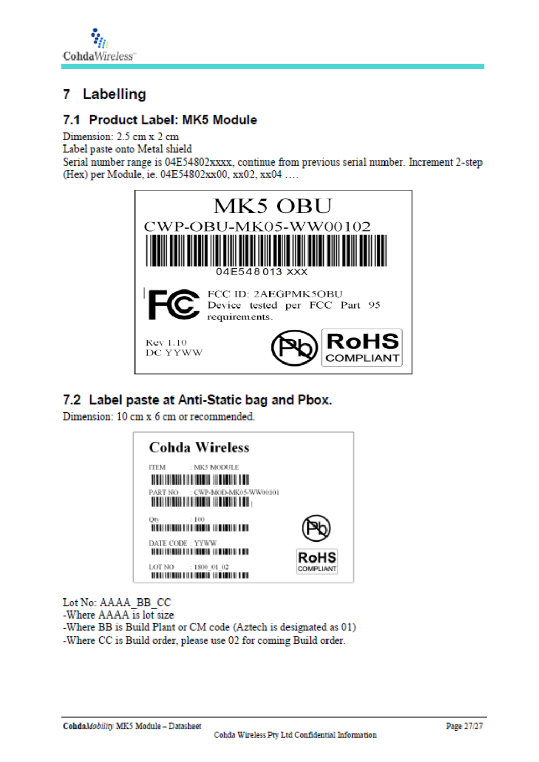
7 Labelling ............................................................................................................... 27
7.1 Product Label: MK5 Module .......................................................................... 27
7.2 Label paste at Anti-Static bag and Pbox. ...................................................... 27
List of Tables
Table 1 - Key Features of the MK5 Module ................................................................................. 6
Table 2 - MK5 Module Receive Sensitivity .................................................................................. 8
Table 3 - Highway NLoS channel parameters .............................................................................. 8
Table 4 - General Transmitter Specification ............................................................................... 10
Table 5 - MK5 Module 5GHz Radio Transmitter Specifications ............................................... 10
Table 6 - Transmitter unwanted emission limits from 1GHz to 18GHz outside the 5GHz ITS
frequency bands ........................................................................................................................... 11
Table 7 - Adjacent Channel Rejection (ACR) ............................................................................ 13
Table 8 - Non-Adjacent Channel Rejection (nACR) .................................................................. 14
Table 9 - Permissible radio path configurations .......................................................................... 16
Table 10 - Module Pin Assignments ........................................................................................... 19
Table 11 - Example circuit Bill of Material ................................................................................ 21
Table 12 - MK5 Module environmental requirements ................................................................ 25

CohdaMobility MK5 Module – Datasheet Page 5/27
Cohda Wireless Pty Ltd Confidential Information

CohdaMobility MK5 Module – Datasheet Page 6/27
Cohda Wireless Pty Ltd Confidential Information
1 Functional Description
1.1 Overview
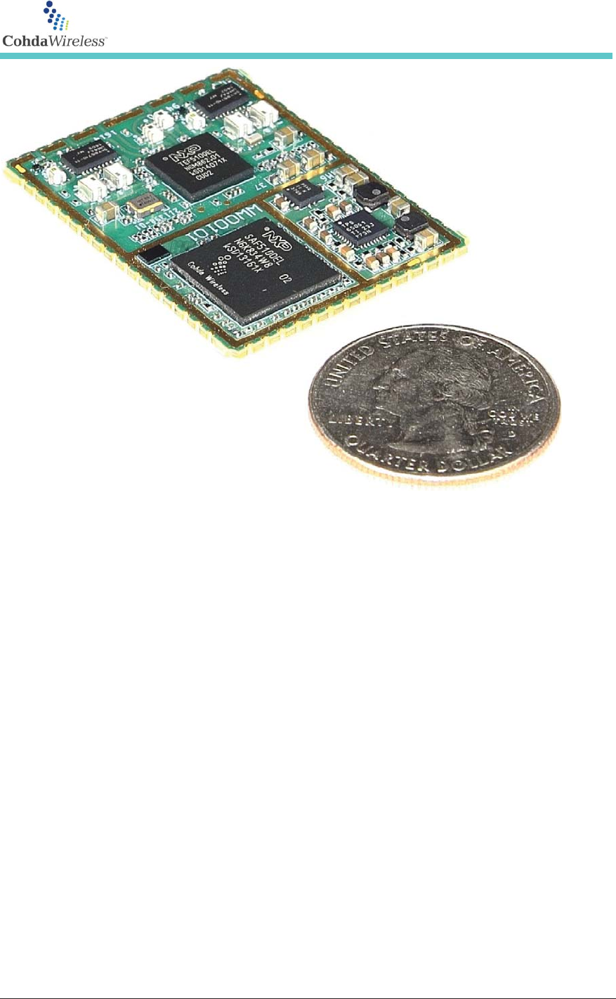
The MK5 Module is designed to provide a compact platform for the deployment of advanced
connected vehicle applications which can exploit the significant performance of the
CohdaMobility Radio in mobile environments.
The MK5 Module is an automotive qualified single or dual channel CohdaMobility IEEE
802.11p radio, operating from -40C to +85C PCB ambient temperature.
The MK5 module is a complete IEEE 802.11p dual-antenna radio, incorporating Link-, MAC-
and PHY Layers and 5.9GHz RF Front-End. It is a surface mount module that only requires
connections to 5.9GHz antennas, USB connection to a host processor, and power supply.
The key features of the MK5 Module are summarised in Table 1below.
Table 1 - Key Features of the MK5 Module
Parameter
Specification
Frequency Bands
5.9 GHz
760 MHz
(Future)
2.4 GHz (Future)
Transmit Power
5.9 GHz: -10 to +23 dBm
5.9 GHz: Class C
Receive Sensitivity
5.9 GHz: -97 dBm
@ 3Mbps
Antenna Diversity
5.9 GHz only:
CDD Transmit Diversity
MRC Receive Diversity
Bandwidth
10 MHz
20 MHz (Future)
Data Rates
3 to 54 Mbps
Power Supply
3.3V
5.0V
Power Consumption
4W (Max)
Temperature Range
-40ºC to +85ºC
Dimensions
40 (L) x 30 (W) x 4 (H) mm
Standards Conformance
IEEE 802.11p – 2010
ETSI ES 202 663
IEEE 1609.4 – 2010

CohdaMobility MK5 Module – Datasheet Page 7/27
Cohda Wireless Pty Ltd Confidential Information
1.2 CohdaMobility MAC
The CohdaMobility MAC implements a full IEEE 802.11p compliant MAC layer, for one or
two independent radio channels. The MAC runs on the ARM processor of the SAF5100.
The CohdaMobility MAC provides fast, time-synchronised channel switching functionality. It
also provides support for multiple queue sets, allowing packets to be queued while the
PHY/MAC is operating on another channel.
The MAC provides the following operating modes:
- Single radio, single channel operation.
o Only one of the radios are used
- Single radio, time-synchronised multi-channel operation
o Channel switching between two channels with independent sets of transmit
queues.
- Dual radio, multi-channel operation
o Independent MAC/PHY entities operating concurrently on different radio
channels.
o Optional coordination between channels to avoid self-interference when
operating on close radio channels.
- Dual radio time synchronised multichannel operation.
o As above, plus one of the radios optionally performs channel switching between
two channels with independent sets of transmit queues
The CohdaMobility MAC provides full IEEE 802.11p support. Full support for MAC time-
synchronisation is provided via an external GNSS receiver under software control or using an
external 1PPS signal.
Other features of the MAC include:
- Radio channel measurements
o Channel utilisation (ratio of channel busy time to measurement duration)
o Channel active ratio (proportion of time that the radio is tuned to the SCH or
CCH, respectively)
o Per-channel statistics (number of packets successfully transmitted, number of
packets that failed to transmit, number of packets successfully received, and
number of packets received in error. Broken down according to broadcast,
multicast, and unicast packets)
o Received signal and noise power levels.
CohdaMobility MK5 Module – Datasheet Page 8/27
Cohda Wireless Pty Ltd Confidential Information
1.3 Performance
1.3.1 Receiver Sensitivity
The receive sensitivity of the MK5 Radio is presented in Table 2 for single and dual receive
antennas, operating at 5.9GHz in DSRC 10MHz bandwidth mode. The packet error rate (PER)
is less than 10% at a PSDU length of 1,000 octets for these input levels. The receive sensitivity
is measured with a signal input directly to the antenna ports. Example plots are presented in
Figure 1 and Figure 2 overleaf.
Table 2 - MK5 Module Receive Sensitivity
Channel
No Multipath [dBm]
Highway NLoS [dBm]
Number of Antennas
1
Typical (Min)
2
Typical (Min)
1
Typical (Min)
2
Typical (Min)
Rate ID
MCS
11
1/2 BPSK
-98 (-95)
-99 (-97)
-95 (-92)
-97 (-95)
15
3/4 BPSK
-96 (-93)
-98 (-96)
-92 (-89)
-95 (-93)
10
1/2 QPSK
-95 (-92)
-97 (-95)
-88 (-85)
-92 (-90)
14
3/4 QPSK
-93 (-90)
-95 (-93)
-86 (-83)
-89 (-87)
9
1/2 16QAM
-90 (-87)
-92 (-90)
-85 (-82)
-88 (-86)
13
3/4 16QAM
-86 (-83)
-88 (-86)
-82 (-79)
-85 (-86)
8
2/3 64QAM
-82 (-79)
-84 (-82)
na
na
12
3/4 64QAM
-80 (-77)
-83 (-81)
na
na
The Highway NLoS (Non Line of Sight) channel parameters used to obtain the values in Table
2 are captured in Table 3 below.
Table 3 - Highway NLoS channel parameters
Tap #
Relative Power [dB]
Delay [ns]
Doppler Frequency [Hz]
0
0
0
0
1
-2
200
689
2
-5
433
-492
3
-7
700
886
This channel was used in the RF testing at the third ETSI Plugtest (CMS3).
Each tap is faded using Pure Doppler, but the second antenna has a Doppler increased by 11Hz,
which prevents phase synchronization of the channels. The Rx Power listed in Table 2 refers to
the power of Tap 0.
The values presented are typical values, measured at +25°C. The sensitivity may be reduced by
approximately 1dB when operating at +85°C or -40°C.
CohdaMobility MK5 Module – Datasheet Page 9/27
Cohda Wireless Pty Ltd Confidential Information
1.3.2 Receiver Maximum Input Level
The receiver maximum operating input level is -20dBm (the PER may exceed 10% for input
levels above this value).
The input level should not exceed 0 dBm to avoid damage.
Figure 1 - Receiver sensitivity for Antenna 1 (No RF multipath)
Figure 2 - Receiver sensitivity for Antenna 2 (No RF multipath)
1.3.3 Transmitter Specifications
Table outlines the transmitter specifications common to all operating modes of the MK5
Module Radio.
CohdaMobility MK5 Module – Datasheet Page 10/27
Cohda Wireless Pty Ltd Confidential Information
Table 4 - General Transmitter Specification
Specification
Performance
Output centre frequency and symbol
clock tolerance.
±10ppm
Transmitter spectral flatness
< ±2 dB in all bandwidth and modulation modes
Transmitter centre frequency leakage
> 15 dB below average sub-carrier power in all
bandwidth and modulation modes
Transmit power control step-size.
0.5 dB
Transmit power control accuracy
±2 dB over temperature
1.3.4 Power Level and Spectral Mask
The MK5 Module Radio maximum output power and spectral mask characteristics are outlined
in Table 5. This specification applies to each of the two 5GHz antenna ports available (Ant1
and Ant2) and targets the entire temperature range. Measured results for the MK5 Module are
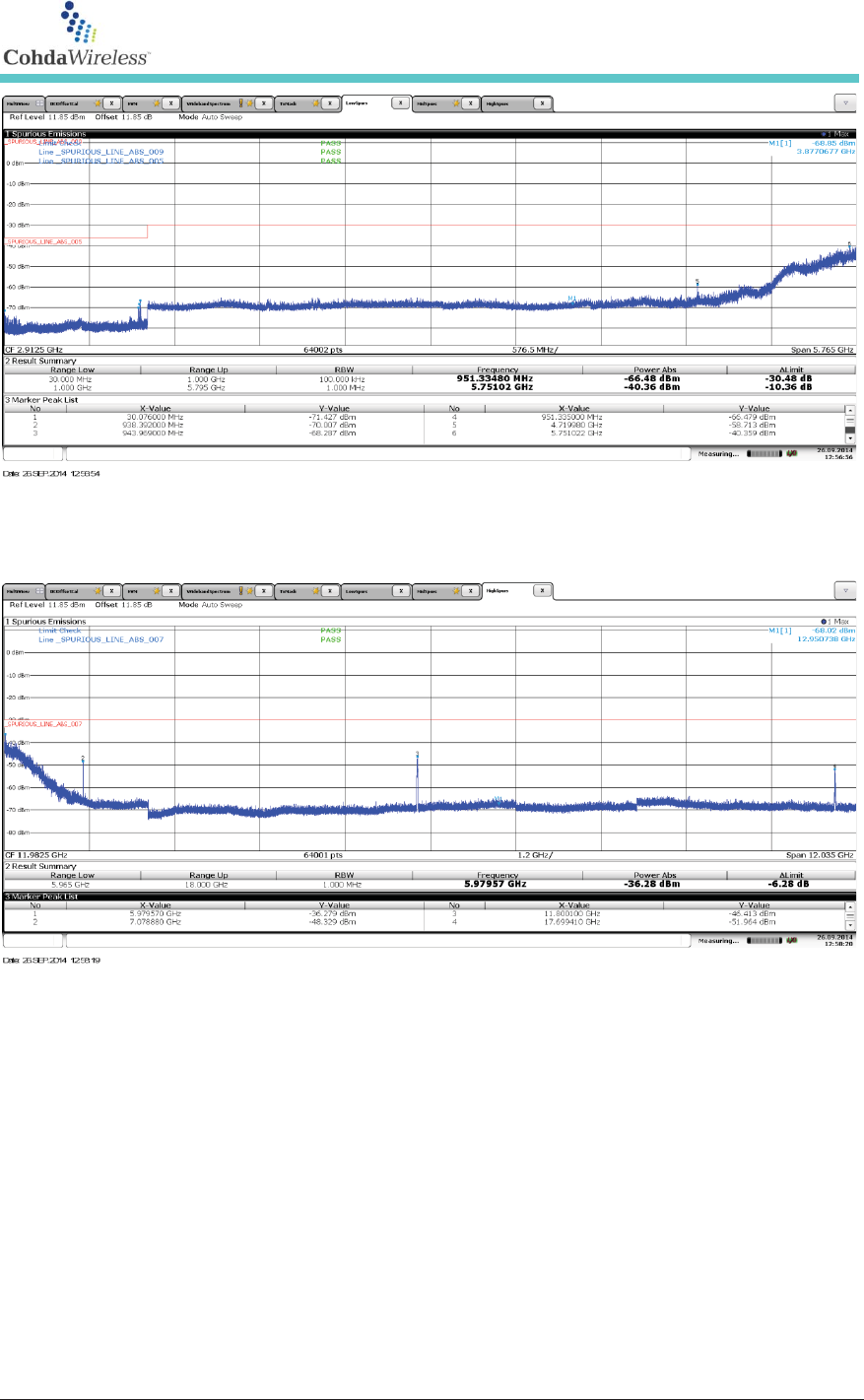
presented in and . Figure 5 and Figure 6 presents typical Out-of-Band unwanted emission
results for the MK5 Module.
Table 5 - MK5 Module 5GHz Radio Transmitter Specifications
Specification
Performance
Maximum Transmit Power
+23dBm per antenna port
(+2
6dBm effective transmit power in 2-
antenna transmit
mode)
Minimum Transmit Power
-10 dBm
Transmit power control
0.5dB steps monotonically increasing/decreasing
EVM
per IEEE802.11-2007 (clause 17.3.9.6.3)
Spectral Mask
Targets DSRC class C,
x 5.0 MHz, -26 dBc
x 5.5 MHz, -32 dBc
x 10 MHz, -40 dBc
x 15 MHz, -50 dBc
Out of Band Emissions
Target ETSI emission mask [EN 302 571] as per Table 6
Supported channels
5GHz: 168-184
CohdaMobility MK5 Module – Datasheet Page 11/27
Cohda Wireless Pty Ltd Confidential Information
Table 6 - Transmitter unwanted emission limits from 1GHz to 18GHz outside the 5GHz ITS frequency
bands
Frequency Range
Res BW
[MHz]
Maximum
Power (EIRP)
[dBm]
1 GHz < f < 5,795 GHz
1
-30
5,795 GHz < f < 5,815 GHz
1
-40
5,815 GHz < f < 5,850 GHz
1
-40
5,850 GHz < f < 5,855 GHz
1
-30
5,925 GHz < f < 5,965 GHz
1
-40
5,965 GHz < f < 18 GHz
1
-30
Figure 3 - MK5 Module Class-C Transmission Mask
Figure 4 - MK5 Module EVM and Transmit Power
CohdaMobility MK5 Module – Datasheet Page 12/27
Cohda Wireless Pty Ltd Confidential Information
Figure 5 - MK5 Module Out-of-Band emission mask (Below DSRC)
Figure 6 - MK5 Module Out-of-Band emission mask (Above DSRC)

CohdaMobility MK5 Module – Datasheet Page 13/27
Cohda Wireless Pty Ltd Confidential Information
1.3.5 Adjacent Channel Rejection
The adjacent channel rejection of a MK5 Module is measured by setting the desired signal
strength 3 dB above the receive sensitivity specified in Table 18-14 of the IEEE802.11-2012
standardTable 2 and raising the power of the interfering signal until 10% PER is caused for a
PSDU length of 1000 octets. The power difference between the interfering and the desired
channel is the corresponding adjacent channel rejection. The interfering signal in the adjacent
channel is a conformant OFDM signal, meeting the DSRC Class C mask, unsynchronized with
the signal in the channel under test. The receive sensitivity values are measured with a signal
input directly to the Antenna Ports. Measured results for the MK5 Module adjacent channel
rejection, together with the target nACR values obtained from the IEEE802.11-2012 standard,
are provided in Table 7
Table 7 - Adjacent Channel Rejection (ACR)
Modulation
Target ACR
[dB]
Target opt. enh. ACR
[dB]
MK5 Typical ACR
[dB]
½ BPSK
16
28
37
¾ BPSK
15
27
33
½ QPSK
13
25
35
¾ QPSK
11
23
29
½ 16QAM
8
20
29
¾ 16QAM
4
16
25
⅔ 64QAM
0
12
22
¾ 64QAM
-1
11
20
CohdaMobility MK5 Module – Datasheet Page 14/27
Cohda Wireless Pty Ltd Confidential Information
1.3.6 Non-Adjacent Channel Rejection
The non-adjacent channel rejection of a MK5 Module Radio is measured by setting the desired
signal’s strength 3 dB above the rate-dependent sensitivity specified in Table 18-14 of the
IEEE802.11-2012, and raising the power of the interfering signal until a 10% PER occurs for a
PSDU length of 1000 octets. The power difference between the interfering and the desired
channel is the corresponding nonadjacent channel rejection. The interfering signal in the non-
adjacent channel is a conformant OFDM signal, targeting the DSRC Class C mask,
unsynchronized with the signal in the channel under test. The receive sensitivity values are
measured with a signal input directly to the Antenna Ports. Measured results for the MK5
Module non-adjacent channel rejection, together with the target nACR values obtained from
the IEEE802.11-2012 standard, are provided in Table 8.
Table 8 - Non-Adjacent Channel Rejection (nACR)
Modulation
Target nACR
[dB]
Target opt. enh. nACR
[dB]
Typical nACR
[dB]
½ BPSK
32
42
51
¾ BPSK
31
41
48
½ QPSK
29
39
48
¾ QPSK
27
37
45
½ 16QAM
24
34
42
¾ 16QAM
20
30
38
⅔ 64QAM
16
26
34
¾ 64QAM
15
25
32
CohdaMobility MK5 Module – Datasheet Page 15/27
Cohda Wireless Pty Ltd Confidential Information
1.3.7 Return Loss
The return loss on all RF ports is no more than -10 dB.
1.3.8 Power Measurements
All receiver power measurements made by MK5 Module (e.g. RSSI) is accurate to r2 dB over
the range of -95 to -20 dBm and over the operating temperature range.
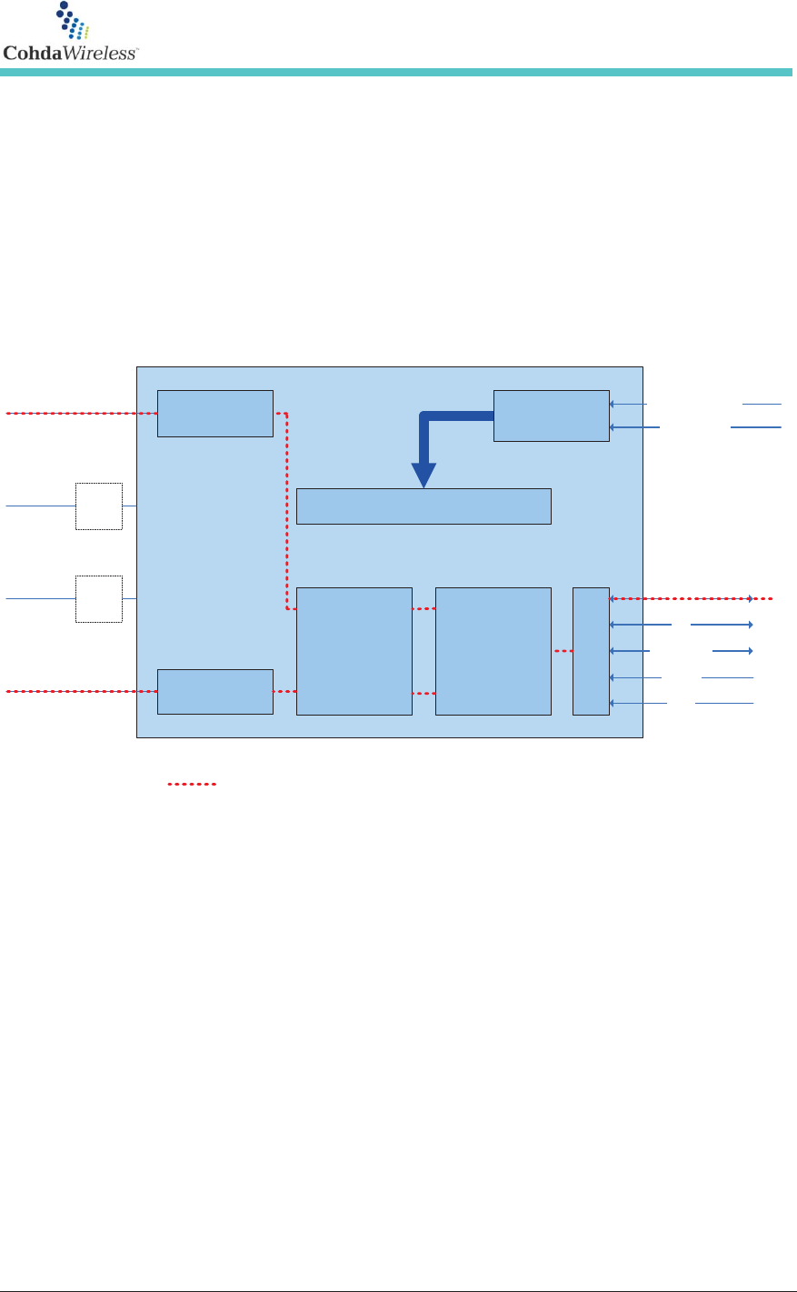
1.4 Block Diagram
MK5 Radio
RF Front-End
RF Front-End
TEF5100 SAF5100
5.9GHz (Ant 1)
IO
USB
SPI
RESET
1PPS
5V0 Analog (RF)
3V3 (Digital)
5.9GHz (Ant 2)
760MHz
2.4GHz
RF
FEM
RF
FEM
Power Supply Decoupling
GPIO (1v8)
Internal
Power Supply
Signal Path
Figure 7 - MK5 HW Block Diagram
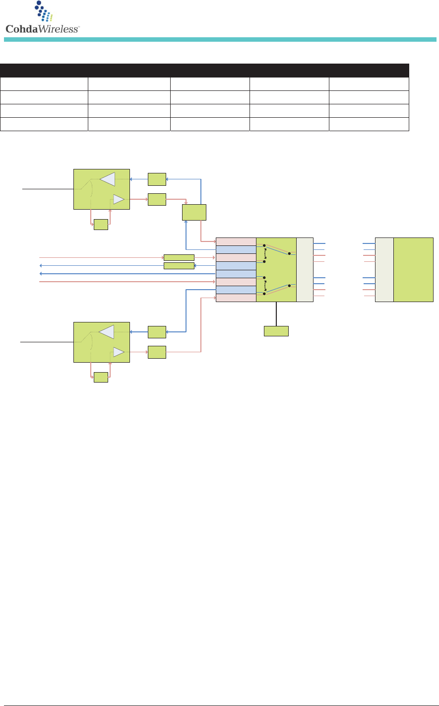
1.5 CohdaMobility DSRC Radio
1.5.1 CohdaMobility PHY
The CohdaMobility PHY is a full IEEE 802.11p compliant physical layer radio transceiver
(PHY) employing the Cohda Wireless advanced mobility receiver algorithms. The PHY RF
front-end can provide multiple radio configurations, allowing the MK5 Module to implement
single or dual radio DSRC systems. The RF sub-system provides separate antenna ports for
5GHz bands via castellated edges of the module. RF output pin sets (separate Rx and Tx pins)
are available for 760MHz and 2.4GHz. These two frequency bands will require off-board RF
Front-End circuits for complete integration into a radio system.
In the dual-radio configuration, the CohdaMobility PHY effectively operates as two
independent PHY modules, each operating on a different radio channel.
The module can support the dual-radio configurations shown in Figure 8.
CohdaMobility MK5 Module – Datasheet Page 16/27
Cohda Wireless Pty Ltd Confidential Information
Table 9 - Permissible radio path configurations
Configuration
5GHz (Ant 1)
5GHz (Ant 2)
760MHz
2.4GHz
1
Yes
Yes
-
-
2
Yes
-
-
Yes
3
-
Yes
Yes
-
4
-
-
Yes
Yes
BPF
BPF
TEF5100
RF5G_1_TX
RF5G_1_RX
RF5G_2_TX
RF5G_2_RX
BB-IF
BPF
BPF
SAF5100
BB-IF
RX1_BB_I_P/N
RX1_BB_Q_P/N
TX1_BB_I_P/N
TR_Out LNA_In
BPF
Rx
Tx TCXO
RF0G7_RX
RF0G7_TX
RF2G4_RX
RF2G4_TX
RF
Bridge
RF5G_ANT_2
RF0G7_TX
RF0G7_RX
RF2G4_RX
TX1_BB_Q_P/N
RX2_BB_I_P/N
RX2_BB_Q_P/N
TX2_BB_I_P/N
TX2_BB_Q_P/N
RF2G4_TX
BALUN
BALUN
TR_Out LNA_In
BPF
Rx
Tx
RF5G_ANT_1
Figure 8 - RF Front-End Block Diagram
The 760MHz and 2.4GHz RF circuits will require external RF Front-End design on host
(carrier) board.
The CohdaMobility PHY provides 2-antenna diversity transmission and reception at 5.9GHz
for optimum radio performance. A summary of the operating modes and functionality of the
CohdaMobility PHY are as follows:
- Single-channel mode (1 or 2 antenna diversity operation).
- Dual-channel mode (1 antenna per channel), 2 independent IEEE 802.11p radios
operating on different radio channels.
- 10MHz (DSRC) channel bandwidth modes.
- Supported frequency bands:
o As per Table 1
- Transmit mask meeting IEEE 802.11p Class C (5GHz band).
- IEEE 802.11p enhanced adjacent channel receiver performance.
- Transmit antenna cyclic delay diversity (2 antenna operation in 5.9 GHz band only).
- Transmit power control (0.5dB steps).
- Fast mode changes for synchronised channel switching systems.

CohdaMobility MK5 Module – Datasheet Page 17/27
Cohda Wireless Pty Ltd Confidential Information
1.5.2 Reset
The reset line will keep the SAF5100 and TEF5100 IC’s on the MK5 module in reset. Contact
Cohda Wireless for specific information on the implementation of this pin.
1.5.3 GPIO
Refer Table 10.
1.5.4 1PPS
The 1PPS input is required by the radio to align transmissions when channel switching and for
timekeeping. The MK5 accepts pulses with standard CMOS 1V8 levels. The signal should have
the rising edge on the UTC second. Pulse width should be 1ms nominally. Pulse widths up to
250ms should be tolerable. As with all MK5 input this signal must NEVER be driven into the
MK5 when the internal MK5 supplies are off. Contact Cohda Wireless for specific information
on the implementation of this pin.
1.5.5 USB
Refer Table 10.
1.5.6 Power Supplies
The MK5 module 5.0v supplies are designed to support up to 400mA current draw for each
radio (producing a continuous sinus wave at maximum transmit power).
The 3.3v power supply is designed to support up to 1A, assuming maximum load on all the
DSP and RF transceiver functions.
The total power consumption of the MK5 module will not exceed 4W in normal operation, and
typically consumes only 2.1W.
CohdaMobility MK5 Module – Datasheet Page 18/27
Cohda Wireless Pty Ltd Confidential Information
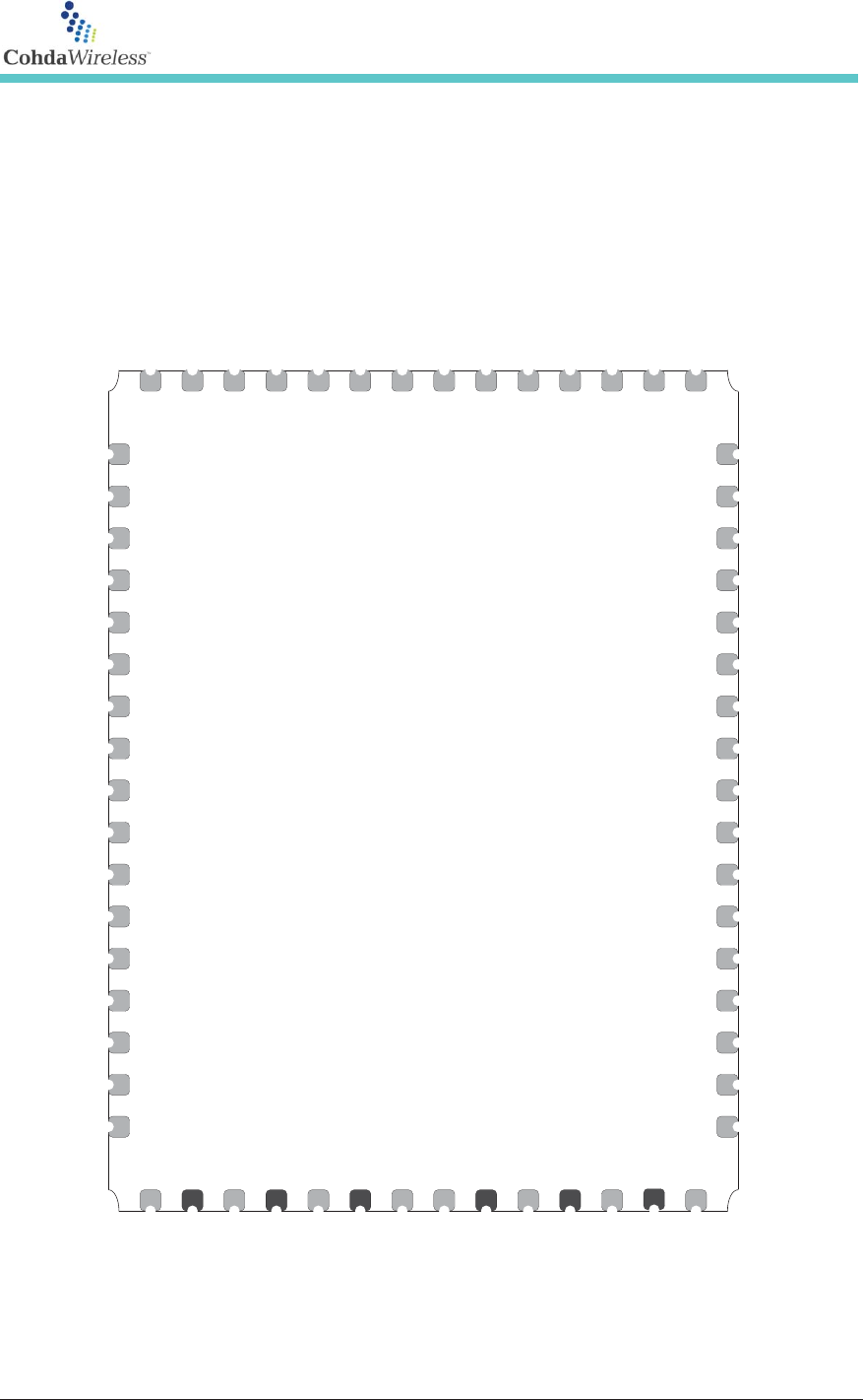
2 Pin Definition
The pin definition for the MK5 Module is presented in Figure below.
All pins marked as N/C should be soldered for mechanical strength with no further electrical
connections.
MK5 Module
(Transparent Top View)
1
2
3
4
5
6
7
8
9
10
11
12
13
14
15
16
17 32
33
34
35
36
37
38
39
40
41
42
43
44
45
46
49
50
51
52
53
54
55
56
57
58
29
28
27
26
25
24
23
22
21
20
19
18
GND
GND
GND
GND
GND
GND
RF5G_ANT_1
GND
31
RF5G_ANT_2
RF2G4_TX
RF2G4_RX
RF0G7_TX
RF0G7_RX
47
59
60
30
GND
48
61
62
N/C
3V3_DIG1
3V3_DIG2
GND
GND
GND
GND
GND
GND
GND
GND
GND
M_RST_N
N/C
N/C
N/C
N/C
N/C
N/C
N/C
N/C
UART1_TX
N/C
GND
N/C
N/C
N/C
N/C
N/C
EXT_PD
RF0G7_X
RF0G7_Y
5V0_PA1 5V0_PA2
RF2G4_Y
RF2G4_X
M_SPI_CS_N
M_SPI_MOSI
M_SPI_MISO
M_SPI_CLK
MOD_IO_SPARE
GPS1PPS_1V8
USB_VBUS
USB_DN
USB_DP
GND
GND
UART1_RX
Figure 9 - MK5 Module transparent top view

CohdaMobility MK5 Module – Datasheet Page 19/27
Cohda Wireless Pty Ltd Confidential Information
Table 10 - Module Pin Assignments
Pin
Assignment
Pin Direction
Description
1
N/C
2
M_RST_N
I
Module Reset (1.8v) 1
3
3V3_DIG1
P
3.3V Power Supply
4
3V3_DIG2
P
3.3V Power Supply
5
GND
P
Ground
6
N/C
See Note 2
7
N/C
8
N/C
9
N/C
10
N/C
11
N/C
12
GND
P
Ground
13
5V0_PA1
P
5.0V Power Supply (RF Ant 1) 4
14
RF0G7_X (N/C)
O
760MHz Control Pin
(N/C for 5.9GHz only modules)
15
RF0G7_Y (N/C)
O
760MHz Control Pin
(N/C for 5.9GHz only modules)
16
GND
P
Ground
17
EXT_PD (N/C)
O
External Power Detect
(N/C for 5.9GHz only modules)
18
GND
P
Ground
19
RF5G_ANT1
O
5.9GHz RF Port (Ant 1)
20
GND
P
Ground
21
RF0G7_TX (N/C)
RF
760MHz RF Output Pin (Tx)
(N/C for 5.9GHz modules)
22
GND
P
Ground
23
RF0G7_RX (N/C)
RF
760MHz RF Input Pin (Rx)
(N/C for 5.9GHz modules)
24
GND
P
Ground
25
GND
P
Ground
26
RF2G4_RX (N/C)
RF
2.4GHz RF Input Pin (Rx)
(N/C for 5.9GHz modules)
27
GND
P
Ground
28
RF2G4_TX (N/C)
RF
2.4GHz RF Output Pin (Tx)
(N/C for 5.9GHz modules)
29
GND
P
Ground
30
RF5G_ANT2
RF
5GHz RF Port (Ant 2)
31
GND
P
Ground
32
GND
P
Ground
33
RF2G4_Y (N/C)
O
2.4GHz Control Pin
(N/C for 5.9GHz only modules
34
RF2G4_X (N/C)
O
2.4GHz Control Pin
(N/C for 5.9GHz only modules
35
GND
P
Ground
36
5V0_PA2
P
5.0V Power Supply (RF Ant 2) 4
37
GND
P
Ground
CohdaMobility MK5 Module – Datasheet Page 20/27
Cohda Wireless Pty Ltd Confidential Information
P=Power I=Input O=Output BI=Bidirectional RF=Radio Frequency
NOTES
1. This pin should be driven by an open drain/collector device. It is internally pulled high to 1V8 by 10k.
When reset it should be below 0.2V.
2. This pin is internally pulled to pin 3 and 4, the 3V3 supply lines. This should not be shorted or pulled to
ground. See HW manual.
3. These 3 pins should never be loaded by more than 500 kΩ to ground or 1V8 as this would interfere with
correct internal operation at boot.
4. The 5V0_PAn pins should have bypass caps located at the pin. These are NOT connected internally and
each supply is isolated to its own PA. Supply must be provided whenever the module main supply is powered.
5. The SPI bus is nominally an output on all modules. Internally, depending upon version of module, there
may be a flash memory on this bus. Direction of these lines may be swapped on some versions of the module
depending upon customer requirements. Always check your modules model and version against the HW
documentation.
6. This line is optionally a SPI CS line. In other cases it may be used as a GPIO. Please check model number
against HW documentation for how to use this pin in your application.
7. The USB interface is only between the module and host processor for short impedance controlled traces.
The data and VBUS signals should only be applied to these pins when the module has power applied otherwise
damage may occur.
8. This UART is not yet implemented but may be used in the future for customer specific or Cohda Wireless
use.
9. This input, as with all inputs, should not be driven in to the device when the power is not supplied to the
module otherwise damage will occur. Contact Cohda Wireless for further information.
38
M_SPI_MOSI
O
Module SPI Bus 5
39
M_SPI_SCK
O
Module SPI Bus 5
40
GND
P
Ground
41
M_SPI_MISO
I
Module SPI Bus 5
42
M_SPI_CS
O
Module SPI Bus 5
43
MOD_IO_SPARE
O
General Purpose IO (1.8V) 6
44
GND
P
Ground
45
M_USB_D_N
BI
Module USB Bus 7
46
M_USB_D_P
BI
Module USB Bus 7
47
GND
P
Ground
48
M_USB_VBUS
P
Module USB Bus 7
49
UART1_RX
I
UART1 Receive Line 8
50
UART1_TX
O
UART1 Transmit line 8
51
GND
P
Ground
52
GPS_1PPS_1V8
I
1PPS Input (1.8v) 9
53
GND
P
Ground
54
N/C
55
N/C
56
N/C
57
N/C
58
N/C
59
N/C
60
GND
P
Ground
61
N/C
62
N/C
CohdaMobility MK5 Module – Datasheet Page 21/27
Cohda Wireless Pty Ltd Confidential Information
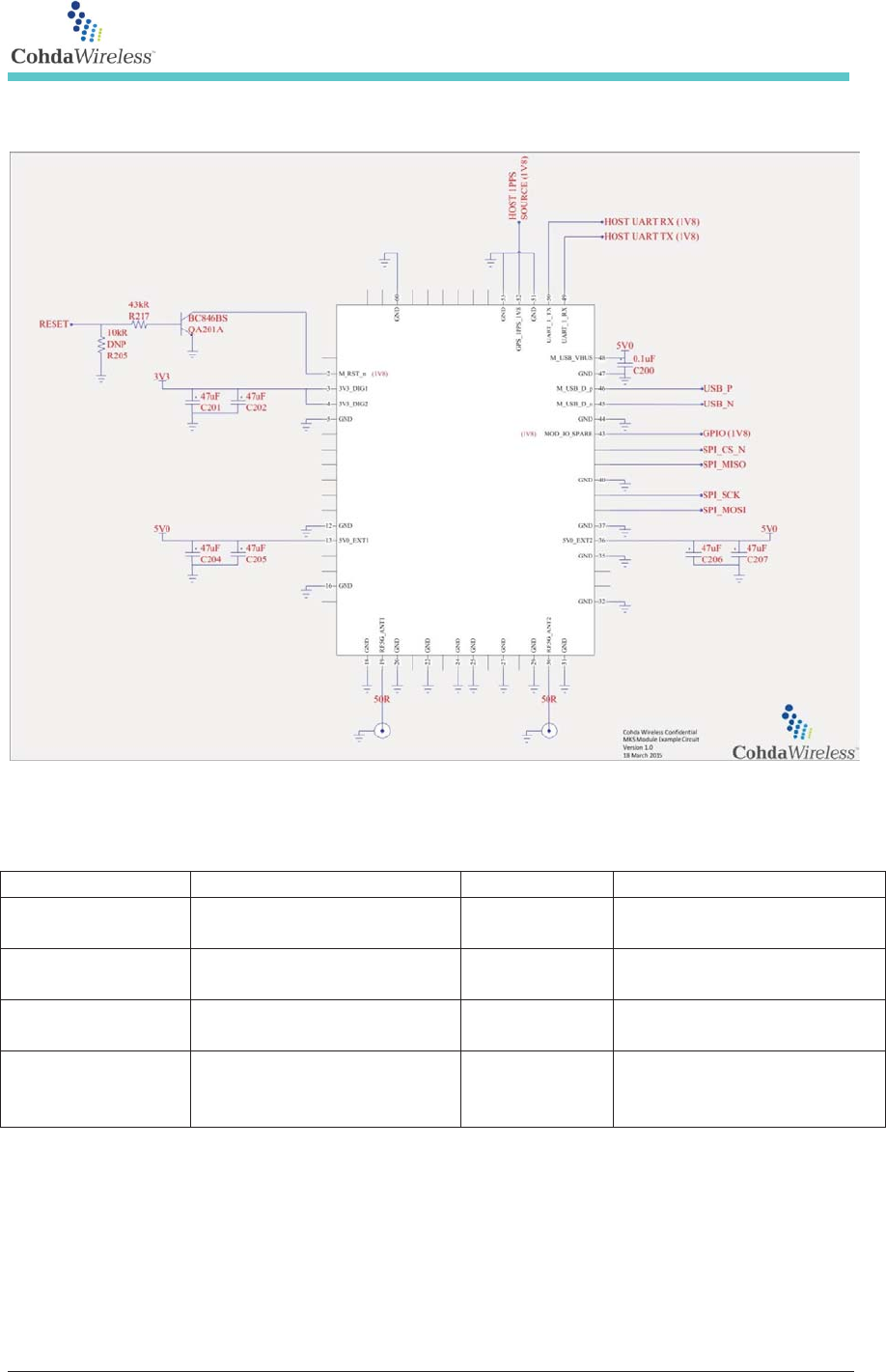
3 Example Circuit
Figure 10 - Example circuit around the MK5 Module
Table 11 - Example circuit Bill of Material
Designator
Part Description
Manufacturer
Manufacturer Part #
C200
CAP CER .1UF 16V X7R
0402
Murata
GRM155R71C104KA88D
C201, C202, C204,
C205, C206, C207
CAP CER 47uF 10V X5R
1206 +/-20%
Taiyo Yuden
LMK316BJ476ML-T
R217, R218
RES CHIP 43k OHM
1/16W 0402 +/-1%
Yageo
RC0402FR-0743KL
QA201A
TRANS NPN/NPN
BC846BS,115 NXP
SOT363
NXP
BC846BS,115
CohdaMobility MK5 Module – Datasheet Page 22/27
Cohda Wireless Pty Ltd Confidential Information
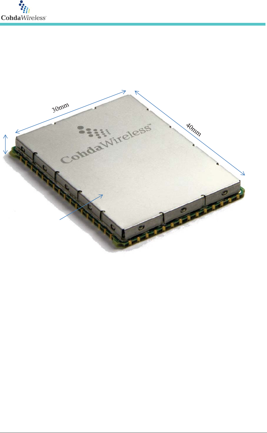
4 Mechanical Specification
The 3D mechanical outline of the MK5 Module is presented in Figure 11 below. The module is
a rectangular unit with dimensions of 40mm x 30mm and a height of approximately 3.5mm.
Figure 11 - 3D Mechanical Outline
3.5mm
RF Shield
CohdaMobility MK5 Module – Datasheet Page 23/27
Cohda Wireless Pty Ltd Confidential Information
Figure 12 - MK5 Module 3D view (no shield)
CohdaMobility MK5 Module – Datasheet Page 24/27
Cohda Wireless Pty Ltd Confidential Information
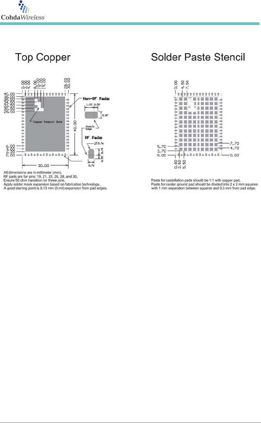
The 2D MK5 Module outline and recommended footprint is shown in Figure 13 below.
Figure 13 - MK5 Module footprint
The castellated RF edges of the MK5 Module require careful routing to Carrier board antenna
connectors. The top layer of the Carrier board should be of high quality low-loss dielectric
material such as Megtron6 or equivalent, with a short RF path to the antenna connectors.

CohdaMobility MK5 Module – Datasheet Page 25/27
Cohda Wireless Pty Ltd Confidential Information
5 Reliability and Compliance
The performance of MK5 Module will be valid over a temperature range of -40C to +85C
(PCB ambient temperature). Table 12 presents a summary of the environmental requirements
on the MK5 Module.
Table 12 - MK5 Module environmental requirements
Item Standard
Vibration ISO 16750-3:2007
Mechanical Shock DIN EN 60068-2-29:1995
Damp Heat IEC 60068-2-30
Drop Test ISO16750-3:2007
DIN EN 60068-2-32:1995
5.1 ESD
The MK5 Module interfaces are designed to withstand a touch discharge of ±15kV
(150Ohm,150pF).
5.2 Regulatory Information
Note: This equipment has been tested and found to comply with the limits for a Class B digital
device, pursuant to part 15 of the FCC Rules. These limits are designed to provide reasonable
protection against harmful interference in a residential installation. This equipment generates,
uses and can radiate radio frequency energy and, if not installed and used in accordance with
the manufacturer’s instructions, may cause harmful interference to radio communications.
CohdaMobility MK5 Module – Datasheet Page 26/27
Cohda Wireless Pty Ltd Confidential Information
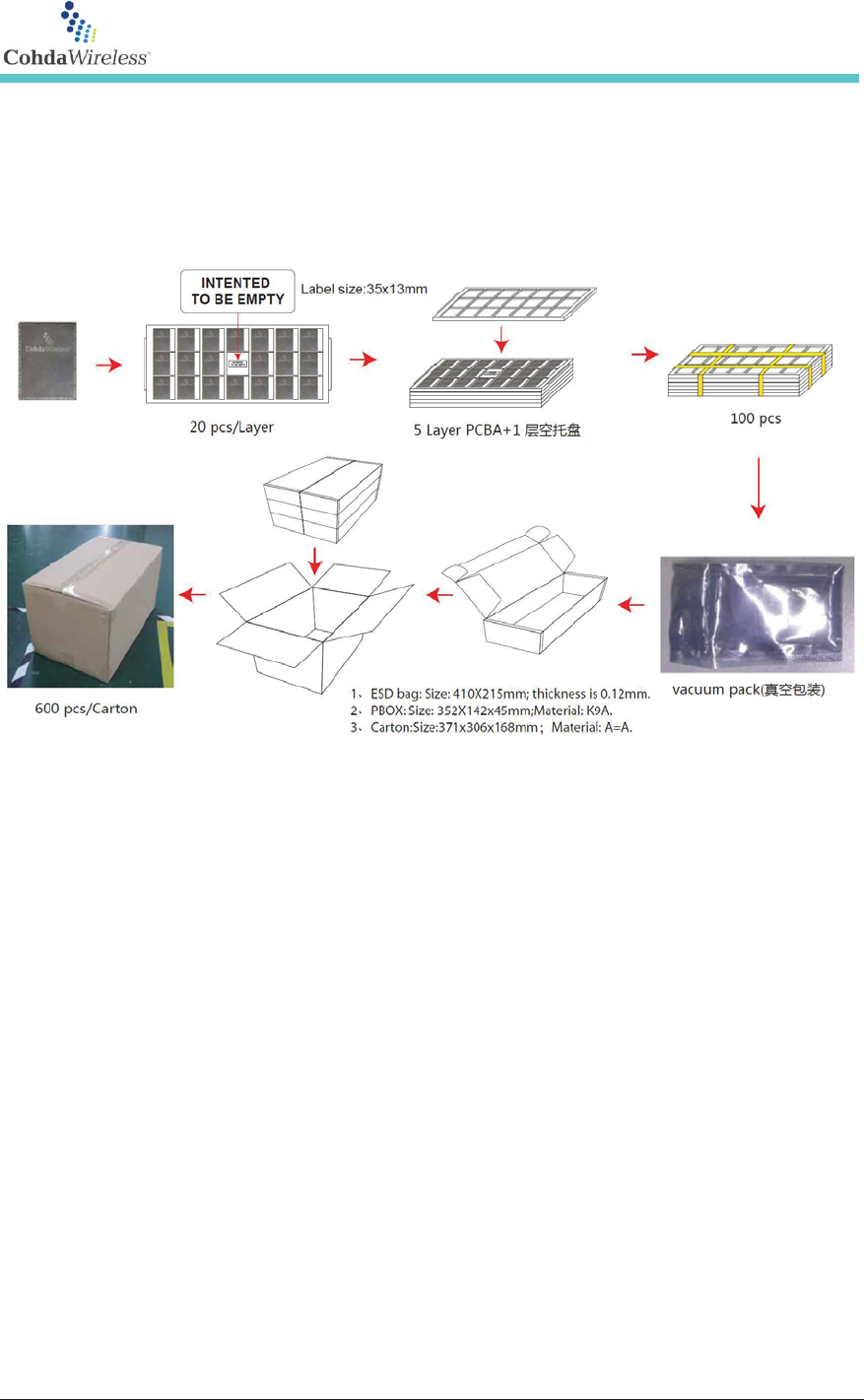
6 Product Packaging and Handling
The MK5 modules are delivered in a standard 40mm x 40mm tray. Small ESD foam is placed
at the tray to prevent the module from movement during shipping and transportation.
The MK5 module is an Electrostatic Sensitive Device (ESD) and require special precautions
when handling. In addition to standard ESD safety practices, the following measures should be
taken into account whenever handling the receiver:
- Unless there is a galvanic coupling between the local GND (i.e. the work table) and the PCB
GND, then the first point of contact when handling the PCB must always be between the local
GND and PCB GND.
- When handling the RF pin, do not come into contact with any charged capacitors and be
careful when contacting materials that can develop charges (e.g. antenna, coax cable ~50-80
pF/m, soldering iron, …)
- To prevent electrostatic discharge through the RF input, do not touch any exposed antenna
area. If there is any risk that such exposed antenna area is touched in non ESD protected work
area, implement proper ESD protection measures in the design.
- When soldering RF connectors and patch antennas to the receiver’s RF pin, make sure to use
an ESD safe soldering iron (tip).
Figure
14 - MK5 Packaging

7.3 End Product Labeling
TheMK5ismarkedwithanFCCID.Itmustbevisibleintheendproduct.IftheMK5isinsidethe
endproduct,thentheremustbealabelpresentontheoutsideoftheproductwiththese
markings:
ContainsModuleFCCID:2AEGPMK5OBU