Communication Network Interface CNI-803D Radio Packet Modem User Manual Users Guide
Communication Network Interface Inc. Radio Packet Modem Users Guide
Users Guide
1
User Guide to
User Guide toUser Guide to
User Guide to
CNI-803D
(Radio Packet Modem)
(Radio Packet Modem)(Radio Packet Modem)
(Radio Packet Modem)
CNI Inc.
CNI Inc.CNI Inc.
CNI Inc.
2
1. Overview _____________________________________________________ 3
2. Specification and features________________________________________ 3
A.Environment ________________________________________________ 3
B.General RF specifications _____________________________________ 3
C.Radio interface ______________________________________________ 3
D.Transmitter_________________________________________________ 4
E.Receiver____________________________________________________ 4
3. Circuit guide____________________________________________________ 5
A. RF circuit _________________________________________________ 5
B. LOGIC Circuit_________________________ ________________ ____7
4. Installation Guide_____________________________ ______________ 9
1. Overview
CNI-803D, RPM(Radio Packet Modem), is a digital data communication equipment in
accordance with RD-LAP19.2 and MDC4800 specification. CNI-803D uses the frequency
ranges from 806MHz to 821Mhz for transmission, and from 851MHz to 866MHz for
reception.
This modem enables you to make data communication in two-way, and it also helps you
to enjoy various types of data services with full mobility due to support for roaming.
With ‘Interface Connector’ you can apply this modem to many kinds of machines to use
‘RD-LAP and MDC Asynchronous Serial Communication (NCL)’ protocol for
communication, and NCL commands enable you to monitor the operation during
communication.
3
! Basic specification
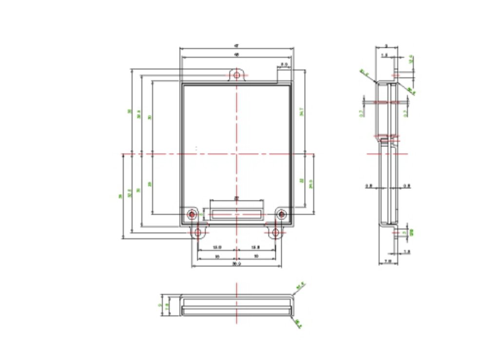
- Dimension : 70 ×47×9mm
- Weight : 37 g
- Supply voltage : 5V
- RF protocol : RD_LAP19.2 on Data TAC4000&5000
Μ∆Χ4800 ον ∆ατα ΤΑΧ4000
- Host protocol : NCL1.2
2. Specification and features
A. Environment
- Operation temperature : -30 ~ +60
- Storage temperature : -35 ~ +80
- Humidity : normal operation after 8 hours storage in 95% non-
condensed
B. General RF specifications
- Modulation : 4FSK for RD-LAP
2ΦΣΚ φορ Μ∆Χ
- Mode : half-duplex
- Bit rate : 19200bps for RD_LAP, 4800bps for MDC
C. Radio interface
- Channel spacing : 25KHz
- Bandwidth : 20KHz
D. Transmitter
Frequency : 806 ~ 821 MHz
Transmit power : 2Watt
Frequency stability : 2.5ppm
Modulation stability : ±10%
FM deviation : 5.6KHz for RD_LAP (Logic +3+3-3-3)
2.5KHz for MDC (Logic +1-1)
Harmonic and Spurious Emission : -60dBc
RX to TX Transition Time : 8ms
E. Receiver
Frequency : 851 ~ 866MHz
Sensitivity Static : -114dBm for the MDC
: -94dBm for the RD_LAP
Adjacent and Alternate Channel Selectivity : 40dB/45dB for the Data
55dB/60dB for the Tone
CO-Channel Decode Ratio : 8dB for the MDC
: 16dB for the RD_LAP
Spurious Response Attenuation : 60dBc
Image Frequency rejection : 50dBc
4
3. Circuit guide
A. RF circuit
CNI-803D circuit is composed of five parts such as power supply, antenna,
synthesis/modulation of frequency, transmission and reception.
1 power supply
Power supply is composed of voltage regulator and switching part. Voltage regulator
generates 3V of power supplied from VBB when the control of RF_EN switch is turned on.
When RF_EN is high, RF_VCC is regulated with 3V, and RF_VCC is supplied to PLL IC,
VCTCXO, OP-Amp(IC102), VCO, and Drive Amp(Q104).
When RX_EN is low, RX_VCC is turned on by Q202, and RX_VCC (3V) is supplied to
LNA, MIXER, IF AMP and IF IC.
When TX_EN is low, TX_VCC is turned on by Q201, and TX_VCC (3V) is supplied to
Buffer Amp(Q105) and OP-Amp(IC104).
The switch between TX mode and RX mode can be achieved by control of RX_EN(Q202)
and TX_EN(Q201).
2 Antenna
Antenna part is composed of antenna matching circuit, BPF, and Rx/Tx signal isolation
circuit.
CNI-803D adapts /4 WHIP antenna to match to mid range frequency of communication.
TX/RX signal isolation circuit isolates signals of communication and is composed of
switching diode and inductor.
The signals received from antenna meet the send/receive path and then D1 is turned on
and the signals proceed only to receiving path. In receiving mode, signals from TX Power
Amp can not go through RX path because D101 is off. (refer to RF circuit diagram)
3 Frequency synthesizer and modulator
Frequency synthesizer consists of PLL part, VCO module and pre-modulation filter. The
PLL part is composed of phase detector, loop filter, and 12.6Mhz VCTCXO
VCO module generates 806~821Mhz frequencies in accordance with the voltage which is
from charge pump of PLL to loop filter. Programmable Divider in PLL makes the VCO
output frequency to any channel value according to the frequency data from Logic CPU.
Phase detector gets low and high frequencies from comparison of phase. Loop filter filters
the frequencies to get a value of voltage. The voltage is input to VCO to achieve phase
lock process.
Modulation is completed when modem IC signal of Logic part is input to VCO and
authorized.
4 Receiver
5
Receiver filters and amplifies RF signal through SAW filter and LNA
RX part is double super heterodyne type, and consists of LNA, LPF, Mixer, SAW filter and
IF IC part. There happens RX signal from antenna and the signal is low-noise-
amplification (LNA) through SAW filter and LNA, and it comes to 2nd IF 455KHz via 2nd
X-TAL44.545MHz.
SAW filter rejects Image frequency(RX ±2*IF) generated from 1’st Mixer while receiving.
For example, if the input channel is 858Mhz, the output frequency would be 45Mhz from
mixer while local frequency is 813Mhz. However, if SAW filter will not filter the image
frequency of 858±2*IF, S/N would be worse with 45Mhz(813-768=45) of noise. And SAW
filter should filter to prevent local frequency becoming spurious through LNA and reverse
path.
LNA amplifies and sends the faint signal from antenna to mixer, and mixer TR mixes and
generates 1st IF with frequency from antenna.
IF comes from mixer. And IF contains inter-modulation product component. MCF
removes that product component. So clean IF(45MHz) can be inserted to IF IC. 2nd local
frequency entered IF IC is mixed with the IF(45MHz) signal to be 2nd IF of 455KHz
simultaneously.
2nd IF signal of 455KHz passes LPF(Ceramic filer) to remove the noise, and the signal is
de-modulated with discriminator method. Here detected RF signal entered into receiver
and RSSI signal which indicates the strength, and they are passed to micro processor in
analogue value.
5 Transmitter
Transmitter consists of driver amp and power amplifier, and TX power control. It
generates carrier frequency while share RX with frequency synthesizer.
Local frequency is used to direct transmission frequency because there is difference
between transmission and reception. So it only amplifies and propagates through PA
(Power Amp.) which can get high level of gain easily with low power.
B. LOGIC Circuit
1 Summary
This unit consists of CPU part, Decoder part, modem part, and power supply part.
2 CPU part(IC3)
The CPU adopted by this unit has 16/32-bit ARM7TDMI RISC processor (66MHz)
and works on 4.9152MHz. The main functions are as follows;
- Execute MASC protocol
- Control PLL circuit of R/F part and perform Power Saving function
- Perform Data transaction function( receiving and transmitting) through Data
Pump(Modem)part
- Checking and processing of RSSI Level come from R/F part
- Perform Data transaction with DTE through DTE interface part
3 Memory part(IC1, IC3)
Memory part consists of FLASH Memory(2Mb, IC1) and SRAM(2Mb, IC3). Flash
6
Memory stores LLI information and program. And SRAM supplies memory stacks for
program.
4 Decoder Part(IC6)
Decoder decodes control signal of CPU and generates SRAM memory choosing
signal.
5 Modem Data Pump(IC7)
Modem part is in charge of NCL protocol , and transmits two way Data between CPU
and RF part. The main functions are as followings ;
- Packet Data Framing
- FSK Data Modulation
- FEC Encoding/Decoding
- Interleaving/De-interleaving
4.Installation Guide
" Modem Descriptions
1. Physical Dimensions
2. Serial Interface between Application DTE
3. Power Supply and Current Usage
" Design Consideration
1. Product Applications
1.1 Use for Portable Terminal
1.2 Use for fixed mount
" Installation
1. Mounting
7
1.1 Fastening
1.2 Grounding
" Warning Label
" Antenna Spec.

8
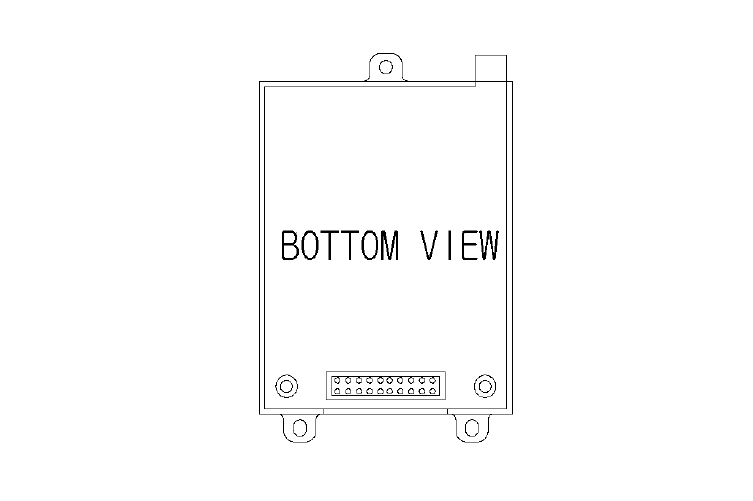
1.physical
Dimensions

10
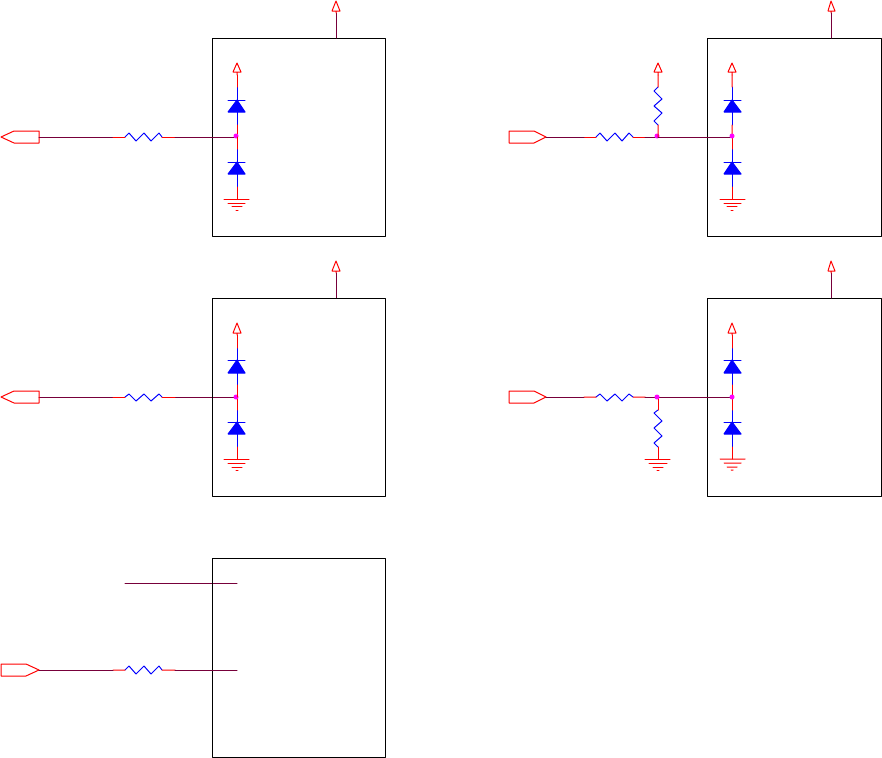
2. Serial Interface Between Application DTE
This unit can be easily integrated into anywhere of the wireless modem adopted
device.
1. RESET : External Reset 11. SENSE4 : Status Input 4
2. TXD : Transmit Data 12. DSR : Data Set Ready
3. PWRON : RPM Power On/Off 13. MAGWAIT : Message Wait
4. RXD : Receive Data 14. DCD : Data Carrier Detect
5. SENSE1 : Status Input 1 15. INRANE : In Range Indicator
6. RTS : Request to Send 16. RI : Ring Indicator
7. SENSE2 : Status Input 2 17. LOWBATT : Low Battery
8. CTS : Clear to Send 18. 5V PWR : 5V Power Supply
9. SENSE3 : Status Input 3 19. GND : Ground to Host
10. DTR : Data Transmit Ready 20. 5V PWR : 5V Power Supply
INTERFACE CIRCUIT OF CNI-803D

11
MSGWAIT
TxDA
22
VCC
HOST
CPU
22
PWRON
LOWBATT
HOST
VCC VCC
SENSE1-4 SENSE
RI
HOST
VCC
CPU
CPU
INRANGE
RTS
22
HOST HOST
VCC
22
22
DSR
RXD
VCCVCC
CPU DTR
INDICATE
RxDA
22
VCC
CPU
22
CTS
VCC
RESET
DCD TXD
12
3. Power Supply and Current Usage
3.1 Example of Power Supply from out-source : input Voltage 5V±10%,
more than 3A
3.1 3.2 Current Usage
TX : 2000mA
RX : 78A
Stand-By : 12mA
Design Considerations
To integrate a wireless modem, there are several issues that need to be addressed and
considered. Internal connections and placement are critical to a successful
implementation. A successful design requires attention to several support
mechanisms as following:
- DC Power
- Serial interface and control
- Mechanical mounting
- Software
- Antenna
- RF control
13
1. Production Applications
The OEM wireless modem is well suited for mobile and fixed applications. The
wireless modem enables user to send/receive data anytime anywhere, and can
provide communications for a wide variety of products
1.1
Portable Terminal Use
Portable designs produce good environment for an integrated modem. The
portable terminal is typically battery powered, subject to temperature extremes,
and designed to be physically strong. When designing portable device, user
needs to pay attention to the following issue:
- DC power noise levels on the host interface
- Minimum operating voltage levels
- Device internal ambient temperature
- Antenna gain and proximity to user
- Mechanical design for drop, vibration, dust, salt and liquid spill.
Note : Regarding this last point, CNI-803D modem is designed on the assumption that
the host device will control these conditions
1.2
Fixed Mount Usage
Fixed-mount usage eliminates most of the mechanical constraints of handheld designs.
The core requirement applies, but fixed usage does not present any special conditions
to address.
" Installation
Installing CNI-803D modem is very simple as follows:
- Place the modem to connector on product housing, and apply a little
force to push it down to be connected.
Caution : Care not to bend or damage the connector pins.
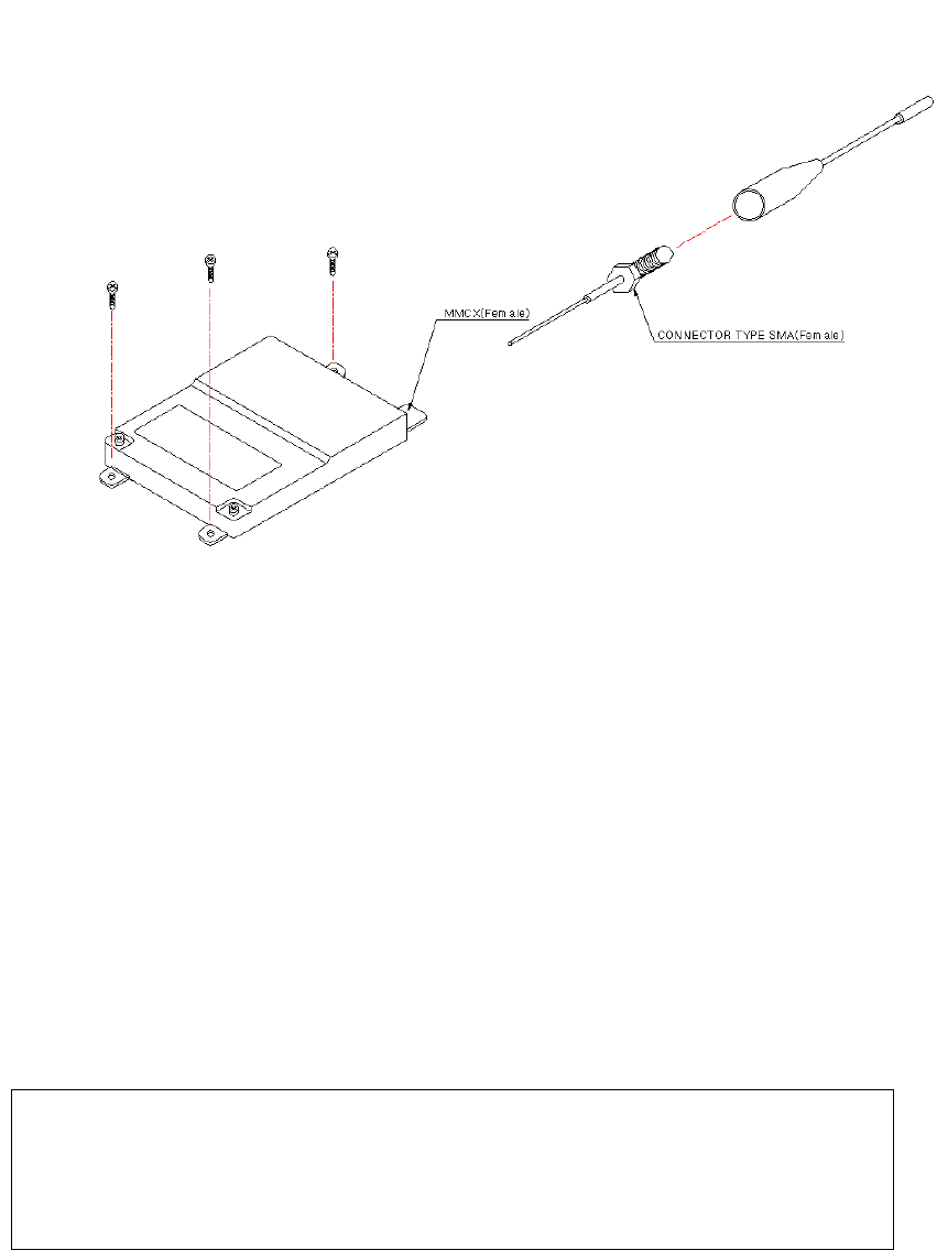
- Use four #2-56 UNC 2A machine screws to tie up the modem as the
figure shown below.
- Connect modem connection cable to a small hole provided at the rear of
the modem.
- Connect the modem connection cable to Antenna

14
1. Mounting
Proper mounting of the modem requires a combination of securely fastening it
within the product housing as well as adequately grounding the modem case to
the housing.
1.1 Fastening
Mount the modem to the rigid OEM product housing by using three #2-56
UNC 2A machine screws as the figure shown below:
1.2 Grounding
For CNI-803D modem, the pin number 19 of connector on the modem is
ground pin. So if user properly places the modem, ground is automatically
done.
" Warning Label
Following warning label shall be attached on the devices using CNI-803D modem.
While this device is in operation, a separation distance of at least 20 centimeters
(7.87 inches) is maintained between radiating antenna and the body of the user
or nearby persons in order to meet the FCC RF exposure guidelines.

15
" Antenna Spec.
Product Name : Whip Antenna of 800MHz Range
MODEL : HA-850W-SSMA
1. Application
Τηισ σπεχιφιχατιον δεσχριβεσ λ/4 WHIP ANTENNA used for frequency range of 800MHz
for τρανσµισσιον ∆ΑΤΑ οφ ωιρελεσσ.
2. Conditions of using Antenna
€ Ηανδηελδ € Φιξεδ € Μοβιλε € Ουτδοορ € Iνδοορ ϒ Οτηερσ
3. Shape of Antenna
Ρεφερ το ατταχηεδ δραωινγ Νο.11Τ−17−003
4. Electrical features and Performance
Item Features/Performance Remark
Frequency range 806 ~ 870 MHz
Nominal impedance 50 Ω
V.S.W.R Below 1 : 2.0
Radiation Omni-direction
Polarization Vertical
Gain Unity
5. Structural Specification

16
Item Specification/Features Remark
Radiator Ø1.5 Speedo wire
Sleeve Shrinkable Tube F-Type Ø1.5
Connector SMA-Plug Ni-plating
Total length 88± 2mm
6. Other features and performance
6.1 Temperature
Antenna shall not be deformed or damaged and shall satisfy “Clause 4” in this specification after
Placing Antenna at –30 and 70 for 96 hours.
6.2 Humidity
After placing Antenna at surrounding temp. 40 ωιτη ρελατιϖε ηυµιδιτψ οφ 90 ∼ 95 φορ 96
ηουρσ, αντεννα σηαλλ νοτ βε δεφορµεδ ορ δαµαγεδ, ανδ σηαλλ σατισφψ “Χλαυσε 4” ιν τηισ
σπεχιφιχατιον