Compaq 850 Users Manual
850 to the manual 6ff48d09-8ea0-49f4-ac93-a4f1c45b66b2
2015-02-03
: Compaq Compaq-850-Users-Manual-468036 compaq-850-users-manual-468036 compaq pdf
Open the PDF directly: View PDF ![]() .
.
Page Count: 252 [warning: Documents this large are best viewed by clicking the View PDF Link!]
- Reader Feedback
- CH1.pdf
- CH2.pdf
- CH3.pdf
- CH4.pdf
- CH5.pdf
- ch6.pdf
- Ch7.pdf
- APPA.pdf
- Appendix A ERROR MESSAGES AND CODES
- INTRODUCTION
- BEEP/KEYBOARD LED CODES
- POWER-ON SELF TEST (POST) MESSAGES
- SYSTEM ERROR MESSAGES (1xx-xx)
- MEMORY ERROR MESSAGES (2xx-xx)
- KEYBOARD ERROR MESSAGES (30x-xx)
- PRINTER ERROR MESSAGES (4xx-xx)
- VIDEO (GRAPHICS) ERROR MESSAGES (5xx-xx)
- DISKETTE DRIVE ERROR MESSAGES (6xx-xx)
- SERIAL INTERFACE ERROR MESSAGES (11xx-xx)
- MODEM COMMUNICATIONS ERROR MESSAGES (12xx-xx)
- SYSTEM STATUS ERROR MESSAGES (16xx-xx)
- HARD DRIVE ERROR MESSAGES (17xx-xx)
- HARD DRIVE ERROR MESSAGES (19xx-xx)
- VIDEO (GRAPHICS) ERROR MESSAGES (24xx-xx)
- AUDIO ERROR MESSAGES (3206-xx)
- DVD/CD-ROM ERROR MESSAGES (33xx-xx)
- NETWORK INTERFACE ERROR MESSAGES (60xx-xx)
- SCSI INTERFACE ERROR MESSAGES (65xx-xx, 66xx-xx, 67xx-xx)
- POINTING DEVICE INTERFACE ERROR MESSAGES (8601-xx)
- Appendix A ERROR MESSAGES AND CODES
- APPB.pdf
- APPC.pdf
- APPD.pdf
- Appe.pdf
- Appf.pdf
- Appg.pdf
- Apph.pdf
- AppI.pdf
- AppJ.pdf
- AppK.pdf
- AppL.pdf
Technical Reference Guide
For
Compaq Deskpro EXS and
Compaq Deskpro Workstation 300 Personal Computers
Featuring the
Intel Pentium 4 Processor
And the
Intel 850 Chipset

This document is designed to allow printing as an 8 ½ x 11-inch hardcopy that will fit into a standard 3-ring
binder. Provided below is a title block that can be copied and/or cut out and placed into a slip or taped onto
the edge of the binder.
Deskpro EXS and Deskpro Workstation 300 Personal Computers
Featuring the Intel Pentium 4 Processor
and the Intel 850 Chipset TRG


Technical Reference Guide
Compaq Deskpro EXS and Workstation 300 Personal Computers
Featuring the Intel Pentium 4 Processor
First Edition - December 2000
i
NOTICE
The information in this document is subject to change without notice.
COMPAQ COMPUTER CORPORATION SHALL NOT BE LIABLE FOR TECHNICAL OR
EDITORIAL ERRORS OR OMISSIONS HEREIN; NOR FOR INCIDENTAL OR
CONSEQUENTIAL DAMAGES RESULTING FROM THE FURNISHING, PERFORMANCE,
OR USE OF THIS MATERIAL. IT IS THE RESPONSIBILITY OF MANUFACTURERS TO
ENSURE THAT DEVICES DESIGNED TO BE USED WITH COMPAQ PRODUCTS
COMPLY WITH FCC CLASS B EMISSIONS REQUIREMENTS.
This guide contains information protected by copyright. Except for use in connection with the
described Compaq product, no part of this document may be photocopied or reproduced in any
form without prior written consent from Compaq Computer Corporation.
2000 Compaq Computer Corporation
All rights reserved. Published in the USA
Compaq, Deskpro, LTE, Contura, Presario, ProLinea
Registered U.S. Patent and Trademark Office
Product names mentioned in this document may be trademarks and/or registered trademarks of other companies.
“Celeron,” “Pentium” and “MMX” are registered trademarks of Intel Corporation.
“Microsoft,” “MS-DOS,” “Windows,” and “Windows NT” are registered trademarks of Microsoft Corporation.
For more information regarding specifications and Compaq-specific parts please contact Compaq
Computer Corporation.
Technical Reference Guide
for
Compaq Deskpro EXS and Workstation 300 Series Personal Computers
First Edition - December 2000
Document Number 13YR-1200A-WWEN

Technical Reference Guide
Compaq Deskpro EXS and Workstation 300 Personal Computers
Featuring the Intel Pentium 4 Processor
First Edition –- December 2000
ii

Technical Reference Guide
Compaq Deskpro EXS and Workstation 300 Personal Computers
Featuring the Intel Pentium 4 Processor
First Edition - December 2000
iii
TABLE OF CONTENTS
CHAPTER 1 INTRODUCTION..................................................................................................................
1.1 ABOUT THIS GUIDE ................................................................................................................ 1-1
1.1.1 USING THIS GUIDE.......................................................................................................... 1-1
1.1.2 ADDITIONAL INFORMATION SOURCES..................................................................... 1-1
1.2 MODEL NUMBERING CONVENTION................................................................................... 1-1
1.3 NOTATIONAL CONVENTIONS.............................................................................................. 1-2
1.3.1 VALUES ............................................................................................................................. 1-2
1.3.2 RANGES ............................................................................................................................. 1-2
1.3.3 SIGNAL LABELS............................................................................................................... 1-2
1.3.4 REGISTER NOTATION AND USAGE............................................................................. 1-2
1.3.5 BIT NOTATION................................................................................................................. 1-2
1.4 COMMON ACRONYMS AND ABBREVIATIONS................................................................. 1-3
CHAPTER 2 SYSTEM OVERVIEW..........................................................................................................
2.1 INTRODUCTION....................................................................................................................... 2-1
2.2 FEATURES AND OPTIONS...................................................................................................... 2-2
2.2.1 STANDARD FEATURES................................................................................................... 2-2
2.2.2 OPTIONS ............................................................................................................................ 2-3
2.3 MECHANICAL DESIGN ........................................................................................................... 2-4
2.3.1 CABINET LAYOUTS ........................................................................................................ 2-4
2.3.2 CHASSIS LAYOUT............................................................................................................ 2-6
2.3.3 BOARD LAYOUT.............................................................................................................. 2-7
2.4 SYSTEM ARCHITECTURE...................................................................................................... 2-8
2.4.1 PENTIUM 4 PROCESSOR............................................................................................... 2-10
2.4.2 CHIPSET........................................................................................................................... 2-11
2.4.3 SUPPORT COMPONENTS.............................................................................................. 2-11
2.4.4 SYSTEM MEMORY......................................................................................................... 2-12
2.4.5 MASS STORAGE............................................................................................................. 2-12
2.4.6 SERIAL, PARALLEL INTERFACES .............................................................................. 2-12
2.4.7 UNIVERSAL SERIAL BUS INTERFACE ...................................................................... 2-12
2.4.8 GRAPHICS SUBSYSTEM ............................................................................................... 2-13
2.4.9 AUDIO SUBSYSTEM...................................................................................................... 2-14
2.5 SPECIFICATIONS ................................................................................................................... 2-14
CHAPTER 3 PROCESSOR/MEMORY SUBSYSTEM ............................................................................
3.1 INTRODUCTION....................................................................................................................... 3-1
3.2 PENTIUM 4 PROCESSOR......................................................................................................... 3-2
3.2.1 PROCESSOR OVERVIEW ................................................................................................ 3-2
3.2.2 PROCESSOR UPGRADING.............................................................................................. 3-4
3.3 MEMORY SUBSYSTEM........................................................................................................... 3-5
3.3.1 RAMBUS ATTRIBUTES................................................................................................... 3-6
3.3.2 RAMBUS CHANNEL TRANSACTIONS .........................................................................3-7
3.3.3 RDRAM POWER MANAGEMENT.................................................................................. 3-8
3.3.4 RDRAM CONFIGURATION/CONTROL ......................................................................... 3-8
3.4 SUBSYSTEM CONFIGURATION.......................................................................................... 3-10

Technical Reference Guide
Compaq Deskpro EXS and Workstation 300 Personal Computers
Featuring the Intel Pentium 4 Processor
First Edition –- December 2000
iv
CHAPTER 4 SYSTEM SUPPORT..............................................................................................................
4.1 INTRODUCTION....................................................................................................................... 4-1
4.2 PCI BUS OVERVIEW................................................................................................................ 4-2
4.2.1 PCI BUS TRANSACTIONS............................................................................................... 4-3
4.2.2 PCI BUS MASTER ARBITRATION ................................................................................. 4-6
4.2.3 OPTION ROM MAPPING.................................................................................................. 4-7
4.2.4 PCI INTERRUPTS.............................................................................................................. 4-7
4.2.5 PCI POWER MANAGEMENT SUPPORT........................................................................ 4-7
4.2.6 PCI SUB-BUSSES .............................................................................................................. 4-7
4.2.7 PCI CONFIGURATION ..................................................................................................... 4-8
4.2.8 PCI CONNECTOR..............................................................................................................4-9
4.3 AGP BUS OVERVIEW ............................................................................................................ 4-10
4.3.1 BUS TRANSACTIONS .................................................................................................... 4-10
4.3.2 AGP CONFIGURATION.................................................................................................. 4-13
4.3.3 AGP CONNECTOR.......................................................................................................... 4-14
4.4 SYSTEM RESOURCES ........................................................................................................... 4-15
4.4.1 INTERRUPTS................................................................................................................... 4-15
4.4.2 DIRECT MEMORY ACCESS.......................................................................................... 4-19
4.5 SYSTEM CLOCK DISTRIBUTION........................................................................................ 4-20
4.6 REAL-TIME CLOCK AND CONFIGURATION MEMORY .................................................4-20
4.6.1 CLEARING CMOS........................................................................................................... 4-21
4.6.2 CMOS ARCHIVE AND RESTORE ................................................................................. 4-22
4.6.3 STANDARD CMOS LOCATIONS.................................................................................. 4-22
4.7 SYSTEM MANAGEMENT...................................................................................................... 4-31
4.7.1 SECURITY FUNCTIONS ................................................................................................ 4-31
4.7.2 POWER MANAGEMENT................................................................................................ 4-32
4.7.3 SYSTEM STATUS ........................................................................................................... 4-33
4.7.4 TEMPERATURE SENSING AND COOLING................................................................ 4-34
4.8 REGISTER MAP AND MISCELLANEOUS FUNCTIONS.................................................... 4-35
4.8.1 SYSTEM I/O MAP ........................................................................................................... 4-35
4.8.2 82801 ICH GENERAL PURPOSE FUNCTIONS ............................................................ 4-36
4.8.3 I/O CONTROLLER FUNCTIONS .................................................................................. 4-37
CHAPTER 5 INPUT/OUTPUT INTERFACES.........................................................................................
5.1 INTRODUCTION....................................................................................................................... 5-1
5.2 ENHANCED IDE INTERFACE................................................................................................. 5-1
5.2.1 IDE PROGRAMMING ....................................................................................................... 5-1
5.2.2 IDE CONNECTOR ............................................................................................................. 5-3
5.3 DISKETTE DRIVE INTERFACE.............................................................................................. 5-4
5.3.1 DISKETTE DRIVE PROGRAMMING................................................................................. 5-5
5.3.2 DISKETTE DRIVE CONNECTOR ...................................................................................... 5-7
5.4 SERIAL INTERFACE ................................................................................................................ 5-8
5.4.1 RS-232 INTERFACE.......................................................................................................... 5-8
5.4.2 SERIAL INTERFACE PROGRAMMING ......................................................................... 5-9
5.5 PARALLEL INTERFACE ........................................................................................................ 5-11
5.5.1 STANDARD PARALLEL PORT MODE......................................................................... 5-11
5.5.2 ENHANCED PARALLEL PORT MODE ........................................................................ 5-12
5.5.3 EXTENDED CAPABILITIES PORT MODE .................................................................. 5-12
5.5.4 PARALLEL INTERFACE PROGRAMMING................................................................. 5-13
5.5.5 PARALLEL INTERFACE CONNECTOR......................................................................5-15

Technical Reference Guide
Compaq Deskpro EXS and Workstation 300 Personal Computers
Featuring the Intel Pentium 4 Processor
First Edition - December 2000
v
5.6 KEYBOARD/POINTING DEVICE INTERFACE................................................................... 5-16
5.6.1 KEYBOARD INTERFACE OPERATION....................................................................... 5-16
5.6.2 POINTING DEVICE INTERFACE OPERATION .......................................................... 5-18
5.6.3 KEYBOARD/POINTING DEVICE INTERFACE PROGRAMMING........................... 5-18
5.6.4 KEYBOARD/POINTING DEVICE INTERFACE CONNECTOR.................................. 5-21
5.7 UNIVERSAL SERIAL BUS INTERFACE .............................................................................. 5-22
5.7.1 USB DATA FORMATS.................................................................................................... 5-22
5.7.2 USB PROGRAMMING.................................................................................................... 5-24
5.7.3 USB CONNECTOR.......................................................................................................... 5-25
5.7.4 USB CABLE DATA ......................................................................................................... 5-25
5.8 AUDIO SUBSYSTEM..............................................................................................................5-26
5.8.1 FUNCTIONAL ANALYSIS ............................................................................................. 5-26
5.8.2 AUDIO CONTROLLER................................................................................................... 5-28
5.8.3 AC97 LINK BUS ..............................................................................................................5-29
5.8.4 AUDIO CODEC................................................................................................................5-30
5.8.5 AUDIO PROGRAMMING ............................................................................................... 5-31
5.8.6 AUDIO SPECIFICATIONS.............................................................................................. 5-32
5.9 NETWORK SUPPORT............................................................................................................. 5-33
5.9.1 PCI VER. 2.2 SUPPORT .................................................................................................. 5-33
5.9.2 ALERT-ON-LAN SUPPORT ........................................................................................... 5-33
5.9.3 REMOTE SYSTEM ALERT SUPPORT.......................................................................... 5-35
CHAPTER 6 POWER SUPPLY AND DISTRIBUTION ..........................................................................
6.1 INTRODUCTION....................................................................................................................... 6-1
6.2 POWER SUPPLY ASSEMBLY/CONTROL .............................................................................6-1
6.2.1 POWER SUPPLY ASSEMBLY ......................................................................................... 6-2
6.2.2 POWER CONTROL ........................................................................................................... 6-3
6.3 POWER DISTRIBUTION .......................................................................................................... 6-5
6.3.1 3.3/5/12 VDC DISTRIBUTION.......................................................................................... 6-5
6.3.2 LOW VOLTAGE PRODUCTION/DISTRIBUTION......................................................... 6-6
6.4 SIGNAL DISTRIBUTION..........................................................................................................6-7
CHAPTER 7 BIOS ROM .............................................................................................................................
7.1 INTRODUCTION....................................................................................................................... 7-1
7.2 ROM FLASHING ....................................................................................................................... 7-2
7.2.1 UPGRADING...................................................................................................................... 7-2
7.2.2 CHANGEABLE SPLASH SCREEN .................................................................................. 7-3
7.3 BOOT FUNCTIONS................................................................................................................... 7-4
7.3.1 BOOT DEVICE ORDER .................................................................................................... 7-4
7.3.2 NETWORK BOOT (F12) SUPPORT................................................................................. 7-4
7.3.3 MEMORY DETECTION AND CONFIGURATION......................................................... 7-5
7.3.4 BOOT ERROR CODES...................................................................................................... 7-5
7.4 SETUP UTILITY........................................................................................................................ 7-6
7.5 CLIENT MANAGEMENT FUNCTIONS................................................................................ 7-12
7.5.1 SYSTEM ID AND ROM TYPE........................................................................................ 7-14
7.5.2 EDID RETRIEVE ............................................................................................................. 7-14
7.5.3 TEMPERATURE STATUS .............................................................................................. 7-14
7.5.4 DRIVE FAULT PREDICTION......................................................................................... 7-15
7.6 PNP SUPPORT ......................................................................................................................... 7-15
7.6.1 SMBIOS ............................................................................................................................ 7-16

Technical Reference Guide
Compaq Deskpro EXS and Workstation 300 Personal Computers
Featuring the Intel Pentium 4 Processor
First Edition –- December 2000
vi
7.7 POWER MANAGEMENT FUNCTIONS ................................................................................ 7-17
7.7.1 INDEPENDENT PM SUPPORT ...................................................................................... 7-17
7.7.2 ACPI SUPPORT................................................................................................................ 7-19
7.7.3 APM 1.2 SUPPORT.......................................................................................................... 7-19
7.8 USB LEGACY SUPPORT........................................................................................................ 7-23
A. APPENDIX A ERROR MESSAGES AND CODES...........................................................................
A.1 INTRODUCTION...................................................................................................................... A-1
A.2 BEEP/KEYBOARD LED CODES............................................................................................. A-1
A.3 POWER-ON SELF TEST (POST) MESSAGES ....................................................................... A-2
A.4 SYSTEM ERROR MESSAGES (1XX-XX) ................................................................................ A-3
A.5 MEMORY ERROR MESSAGES (2XX-XX) .............................................................................. A-4
A.6 KEYBOARD ERROR MESSAGES (30X-XX) .......................................................................... A-4
A.7 PRINTER ERROR MESSAGES (4XX-XX)................................................................................ A-5
A.8 VIDEO (GRAPHICS) ERROR MESSAGES (5XX-XX)............................................................. A-5
A.9 DISKETTE DRIVE ERROR MESSAGES (6XX-XX)................................................................ A-6
A.10 SERIAL INTERFACE ERROR MESSAGES (11XX-XX).......................................................... A-6
A.11 MODEM COMMUNICATIONS ERROR MESSAGES (12XX-XX) ......................................... A-7
A.12 SYSTEM STATUS ERROR MESSAGES (16XX-XX) .............................................................. A-8
A.13 HARD DRIVE ERROR MESSAGES (17XX-XX)...................................................................... A-8
A.14 HARD DRIVE ERROR MESSAGES (19XX-XX)...................................................................... A-9
A.15 VIDEO (GRAPHICS) ERROR MESSAGES (24XX-XX)........................................................... A-9
A.16 AUDIO ERROR MESSAGES (3206-XX)................................................................................ A-10
A.17 DVD/CD-ROM ERROR MESSAGES (33XX-XX)................................................................... A-10
A.18 NETWORK INTERFACE ERROR MESSAGES (60XX-XX) ................................................. A-10
A.19 SCSI INTERFACE ERROR MESSAGES (65XX-XX, 66XX-XX, 67XX-XX) ............................ A-11
A.20 POINTING DEVICE INTERFACE ERROR MESSAGES (8601-XX).................................... A-11
APPENDIX B ASCII CHARACTER SET..................................................................................................
B.1 INTRODUCTION.......................................................................................................................B-1
APPENDIX C KEYBOARD.........................................................................................................................
C.1 INTRODUCTION.......................................................................................................................C-1
C.2 KEYSTROKE PROCESSING ....................................................................................................C-2
C.2.1 PS/2-TYPE KEYBOARD TRANSMISSIONS...................................................................C-3
C.2.2 USB-TYPE KEYBOARD TRANSMISSIONS...................................................................C-4
C.2.3 KEYBOARD LAYOUTS....................................................................................................C-5
C.2.4 KEYS...................................................................................................................................C-8
C.2.5 KEYBOARD COMMANDS.............................................................................................C-11
C.2.6 SCAN CODES...................................................................................................................C-11
C.3 CONNECTORS.........................................................................................................................C-16

Technical Reference Guide
Compaq Deskpro EXS and Workstation 300 Personal Computers
Featuring the Intel Pentium 4 Processor
First Edition - December 2000
vii
APPENDIX D COMPAQ/NVIDIA TNT2 PRO AGP GRAPHICS CARD..............................................
D.1 INTRODUCTION...................................................................................................................... D-1
D.2 FUNCTIONAL DESCRIPTION................................................................................................ D-2
D.3 DISPLAY MODES .................................................................................................................... D-3
D.4 SOFTWARE SUPPORT INFORMATION ............................................................................... D-4
D.5 POWER MANAGEMENT AND CONSUMPTION ................................................................. D-4
D.6 CONNECTORS.......................................................................................................................... D-5
D.6.1 MONITOR CONNECTOR ................................................................................................ D-5
APPENDIX E COMPAQ/NVIDIA GEFORCE2 GTS AGP GRAPHICS CARD...................................
E.1 INTRODUCTION.......................................................................................................................E-1
E.2 FUNCTIONAL DESCRIPTION.................................................................................................E-2
E.3 DISPLAY MODES .....................................................................................................................E-3
E.4 SOFTWARE SUPPORT INFORMATION ................................................................................E-4
E.5 POWER MANAGEMENT AND CONSUMPTION ..................................................................E-4
E.6 CONNECTORS...........................................................................................................................E-5
E.6.1 MONITOR CONNECTOR .................................................................................................E-5
E.6.2 VIDEO FEATURE CONNECTOR.....................................................................................E-6
APPENDIX F COMPAQ/LUCENT V.90 56K PCI MODEM ..................................................................
F.1 INTRODUCTION.......................................................................................................................F-1
F.2 FUNCTIONAL DESCRIPTION.................................................................................................F-2
F.3 OPERATING PARAMETERS ...................................................................................................F-3
F.3.1 UART TRANSFER RATES................................................................................................F-3
F.3.2 TRANSMISSION MODES.................................................................................................F-3
F.4 POWER MANAGEMENT .........................................................................................................F-4
F.4.1 APM ENVIRONMENT ......................................................................................................F-4
F.4.2 ACPI ENVIRONMENT......................................................................................................F-4
F.5 PROGRAMMING.......................................................................................................................F-4
F.6 CONNECTOR.............................................................................................................................F-4
APPENDIX G COMPAQ/ELSA GLORIA II GRAPHICS CARD...........................................................
G.1 INTRODUCTION...................................................................................................................... G-1
G.2 FUNCTIONAL DESCRIPTION................................................................................................ G-2
G.3 DISPLAY MODES .................................................................................................................... G-3
G.4 SOFTWARE SUPPORT INFORMATION ............................................................................... G-4
G.5 POWER MANAGEMENT AND CONSUMPTION ................................................................. G-4
G.6 CONNECTORS.......................................................................................................................... G-5
G.6.1 MONITOR CONNECTOR ................................................................................................ G-5
G.6.2 VIDEO FEATURE CONNECTOR.................................................................................... G-6

Technical Reference Guide
Compaq Deskpro EXS and Workstation 300 Personal Computers
Featuring the Intel Pentium 4 Processor
First Edition –- December 2000
viii
APPENDIX H COMPAQ/MATROX MILLENNIUM G450 AGP GRAPHICS CARD ........................
H.1 INTRODUCTION...................................................................................................................... H-1
H.2 FUNCTIONAL DESCRIPTION................................................................................................ H-2
H.3 DISPLAY MODES .................................................................................................................... H-3
H.4 SOFTWARE SUPPORT INFORMATION ............................................................................... H-4
H.5 POWER MANAGEMENT AND CONSUMPTION ................................................................. H-4
H.6 CONNECTORS.......................................................................................................................... H-5
H.6.1 MONITOR CONNECTOR ................................................................................................ H-5
H.6.2 VIDEO FEATURE CONNECTOR.................................................................................... H-6
APPENDIX I COMPAQ/INTEL NETWORK INTERFACE CONTROLLER ADAPTERS................
I.1 INTRODUCTION........................................................................................................................I-1
I.2 FUNCTIONAL DESCRIPTION..................................................................................................I-2
I.2.1 AOL FUNCTION.....................................................................................................................I-3
I.2.2 WAKE UP FUNCTIONS.........................................................................................................I-3
I.2.3 IPSEC FUNCTION..................................................................................................................I-4
I.3 POWER MANAGEMENT SUPPORT........................................................................................I-5
I.3.1 APM ENVIRONMENT ...........................................................................................................I-5
I.3.2 ACPI ENVIRONMENT...........................................................................................................I-5
I.4 ADAPTER PROGRAMMING....................................................................................................I-6
I.4.1 CONFIGURATION .................................................................................................................I-6
I.4.2 CONTROL ...............................................................................................................................I-6
I.5 NETWORK CONNECTOR.........................................................................................................I-7
I.6 ADAPTER SPECIFICATIONS ...................................................................................................I-7
APPENDIX J COMPAQ/NVIDIA QUADRO2 MXR AGP GRAPHICS CARD....................................
J.1 INTRODUCTION........................................................................................................................J-1
J.2 FUNCTIONAL DESCRIPTION..................................................................................................J-2
J.3 DISPLAY MODES ......................................................................................................................J-3
J.4 SOFTWARE SUPPORT INFORMATION .................................................................................J-4
J.5 POWER MANAGEMENT AND CONSUMPTION ...................................................................J-4
J.6 CONNECTORS............................................................................................................................J-5
J.6.1 MONITOR CONNECTOR ..................................................................................................J-5
APPENDIX K COMPAQ PCI 10/100 ETHERNET ADAPTER ..............................................................
K.1 INTRODUCTION...................................................................................................................... K-1
K.2 FUNCTIONAL DESCRIPTION................................................................................................ K-2
K.2.1 AOL FUNCTION.................................................................................................................K-3
K.2.2 RSA FUNCTION..................................................................................................................K-4
K.2.3 WAKE UP FUNCTIONS .....................................................................................................K-4
K.3 POWER MANAGEMENT SUPPORT...................................................................................... K-5
K.3.1 APM ENVIRONMENT ..................................................................................................... K-5
K.3.2 ACPI ENVIRONMENT..................................................................................................... K-5
K.4 CONNECTORS.......................................................................................................................... K-6
K.4.1 NETWORK CONNECTOR............................................................................................... K-6

Technical Reference Guide
Compaq Deskpro EXS and Workstation 300 Personal Computers
Featuring the Intel Pentium 4 Processor
First Edition - December 2000
ix
K.4.2 AOL/SOS CONNECTOR .................................................................................................. K-6
K.4.3 SMBUS CONNECTOR ..................................................................................................... K-7
K.4.4 WOL CONNECTOR.......................................................................................................... K-7
K.5 ADAPTER SPECIFICATIONS ................................................................................................. K-8
APPENDIX L COMPAQ/ADAPTEC SCSI HOST ADAPTER................................................................
L.1 INTRODUCTION.......................................................................................................................L-1
L.2 FUNCTIONAL DESCRIPTION.................................................................................................L-2
L.3 SCSI ADAPTER PROGRAMMING ..........................................................................................L-3
L.3.1 SCSI ADAPTER CONFIGURATION................................................................................L-3
L.3.2 SCSI ADAPTER CONTROL..............................................................................................L-3
L.4 SPECIFICATIONS .....................................................................................................................L-3
L.5 SCSI CONNECTORS .................................................................................................................L-4
L.5.1 EXTERNAL 50-PIN ULTRA SCSI CONNECTOR...........................................................L-4
L.5.2 INTERNAL 50-PIN ULTRA SCSI CONNECTOR............................................................L-5
L.5.3 INTERNAL 68-PIN ULTRA160 SCSI CONNECTOR......................................................L-6

Technical Reference Guide
Compaq Deskpro EXS and Workstation 300 Personal Computers
Featuring the Intel Pentium 4 Processor
First Edition –- December 2000
x
LIST OF FIGURES
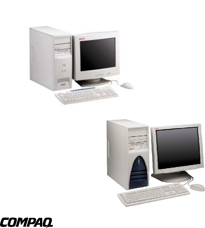
FIGURE 2–1. COMPAQ DESKPRO PERSONAL COMPUTERS WITH MONITORS................................................ 2-1
FIGURE 2–2. FRONT CABINET VIEWS ......................................................................................................... 2-4
FIGURE 2–3. REAR CABINET VIEW............................................................................................................. 2-5
FIGURE 2–4. CHASSIS LAYOUT, LEFT SIDE VIEW ....................................................................................... 2-6
FIGURE 2–5. SYSTEM BOARD LAYOUT...................................................................................................... 2-7
FIGURE 2–6. SYSTEM ARCHITECTURE, BLOCK DIAGRAM ............................................................................ 2-9
FIGURE 2–7. PROCESSOR ASSEMBLY AND MOUNTING............................................................................. 2-10
FIGURE 3–1. PROCESSOR/MEMORY SUBSYSTEM ARCHITECTURE.............................................................. 3-1
FIGURE 3–2. PENTIUM 4 PROCESSOR INTERNAL ARCHITECTURE............................................................... 3-3
FIGURE 3–3. SDRAM/RDRAM BANDWIDTH COMPARISON...................................................................... 3-5
FIGURE 3–4. RAMBUS CHANNEL SIGNAL DISTRIBUTION AND KEY ATTRIBUTES ........................................ 3-6
FIGURE 3–5. RAMBUS TRANSACTIONS (SINGLE CHANNEL)........................................................................ 3-7
FIGURE 3–6. SYSTEM MEMORY MAP ......................................................................................................... 3-9
FIGURE 4-1. PCI BUS DEVICES AND FUNCTIONS......................................................................................... 4-2
FIGURE 4-2. CONFIGURATION CYCLE ......................................................................................................... 4-4
FIGURE 4-3. PCI CONFIGURATION SPACE MAPPING................................................................................... 4-5
FIGURE 4-4. PCI BUS CONNECTOR (32-BIT TYPE) ..................................................................................... 4-9
FIGURE 4-5. AGP 1X DATA TRANSFER (PEAK TRANSFER RATE: 266 MB/S).......................................... 4-11
FIGURE 4-6. AGP 2X DATA TRANSFER (PEAK TRANSFER RATE: 532 MB/S).......................................... 4-12
FIGURE 4-7. AGP 4X DATA TRANSFER (PEAK TRANSFER RATE: 1064 MB/S)........................................ 4-12
FIGURE 4-8. 1.5-VOLT AGP BUS CONNECTOR......................................................................................... 4-14
FIGURE 4-9. MASKABLE INTERRUPT PROCESSING, BLOCK DIAGRAM ...................................................... 4-15
FIGURE 4-10. CONFIGURATION MEMORY MAP......................................................................................... 4-20
FIGURE 4-11. FAN CONTROL BLOCK DIAGRAM......................................................................................... 4-34
FIGURE 5-1. 40-PIN PRIMARY IDE CONNECTOR (ON SYSTEM BOARD). ...................................................... 5-3
FIGURE 5-2. 34-PIN DISKETTE DRIVE CONNECTOR..................................................................................... 5-7
FIGURE 5-3. SERIAL INTERFACE CONNECTOR (MALE DB-9 AS VIEWED FROM REAR OF CHASSIS)............... 5-8
FIGURE 5-4. PARALLEL INTERFACE CONNECTOR (FEMALE DB-25 AS VIEWED FROM REAR OF CHASSIS)..5-15
FIGURE 5-5. KEYBOARD OR POINTING DEVICE INTERFACE CONNECTOR .................................................. 5-21
FIGURE 5-6. USB I/F, BLOCK DIAGRAM................................................................................................... 5-22
FIGURE 5-7. USB PACKET FORMATS........................................................................................................ 5-23
FIGURE 5-8. UNIVERSAL SERIAL BUS CONNECTOR................................................................................... 5-25
FIGURE 5-9. AUDIO SUBSYSTEM FUNCTIONAL BLOCK DIAGRAM ............................................................. 5-27
FIGURE 5-10. AC’97 LINK BUS PROTOCOL .............................................................................................. 5-29
FIGURE 5-11. CS4297A AUDIO CODEC FUNCTIONAL BLOCK DIAGRAM................................................... 5-30
FIGURE 5-12. AOL IMPLEMENTATION (GENERIC REPRESENTATION) ....................................................... 5-34
FIGURE 5-13. REMOTE SENSE ALERT IMPLEMENTATION (GENERIC REPRESENTATION)............................ 5-35
FIGURE 5-14. RSA LOGIC, BLOCK DIAGRAM ........................................................................................... 5-35
FIGURE 6–1. POWER DISTRIBUTION AND CONTROL, BLOCK DIAGRAM....................................................... 6-1
FIGURE 6–2. POWER CABLE DIAGRAM....................................................................................................... 6-5
FIGURE 6–3. LOW VOLTAGE SUPPLY AND DISTRIBUTION DIAGRAM........................................................... 6-6
FIGURE 6–4. SIGNAL DISTRIBUTION DIAGRAM, TYPICAL CONFIGURATION ................................................ 6-7
FIGURE 6–5. HEADER PINOUTS .................................................................................................................. 6-8
FIGURE B–1. ASCII CHARACTER SET........................................................................................................B-1

Technical Reference Guide
Compaq Deskpro EXS and Workstation 300 Personal Computers
Featuring the Intel Pentium 4 Processor
First Edition - December 2000
xi
FIGURE C–1. KEYSTROKE PROCESSING ELEMENTS, BLOCK DIAGRAM ......................................................C-2
FIGURE C–2. PS/2 KEYBOARD-TO-SYSTEM TRANSMISSION, TIMING DIAGRAM ........................................C-3
FIGURE C–3. U.S. ENGLISH (101-KEY) KEYBOARD KEY POSITIONS..........................................................C-5
FIGURE C–4. NATIONAL (102-KEY) KEYBOARD KEY POSITIONS...............................................................C-5
FIGURE C–5. U.S. ENGLISH WINDOWS (101W-KEY) KEYBOARD KEY POSITIONS.....................................C-6
FIGURE C–6. NATIONAL WINDOWS (102W-KEY) KEYBOARD KEY POSITIONS ..........................................C-6
FIGURE C–7. 7-BUTTON EASY ACCESS KEYBOARD LAYOUT.....................................................................C-7
FIGURE C–8. 8-BUTTON EASY ACCESS KEYBOARD LAYOUT.....................................................................C-7
FIGURE C–9. PS/2 KEYBOARD CABLE CONNECTOR (MALE)....................................................................C-16
FIGURE C–10. USB KEYBOARD CABLE CONNECTOR (MALE) .................................................................C-16
FIGURE D-1. COMPAQ/NVIDIA TNT2 PRO AGP GRAPHICS CARD (P/N 198998-B21) LAYOUT .............D-1
FIGURE D-2. NVIDIA TNT2 PRO GRAPHICS CARD BLOCK DIAGRAM.........................................................D-2
FIGURE D-3. VGA MONITOR CONNECTOR, (FEMALE DB-15, AS VIEWED FROM REAR)...............................D-5
FIGURE E-1. COMPAQ/NVIDIA GEFORCE2 GTS AGP GRAPHICS CARD (P/N 179642-001) LAYOUT......E-1
FIGURE E-2. NVIDIA GEFORCE2 GTS GRAPHICS CARD BLOCK DIAGRAM ................................................E-2
FIGURE E-3. VGA MONITOR CONNECTOR, (FEMALE DB-15, AS VIEWED FROM REAR). ..............................E-5
FIGURE E-4. FEATURE CONNECTOR (26-PIN HEADER).................................................................................E-6
FIGURE F-1. COMPAQ/LUCENT V.90 56K PCI MODEM (PCA #152972) LAYOUT..................................... F-1
FIGURE F-2. COMPAQ/LUCENT V.90 56K PCI MODEM BLOCK DIAGRAM ................................................... F-2
FIGURE F-3. RJ-11 CONNECTOR, (FEMALE, AS VIEWED FROM REAR). ......................................................... F-4
FIGURE G-1. COMPAQ/ELSA GLORIA II AGP GRAPHICS CARD (P/N 174565-001) LAYOUT ...................G-1
FIGURE G-2. ELSA GLORIA II GRAPHICS CARD BLOCK DIAGRAM ..............................................................G-2
FIGURE G-3. VGA MONITOR CONNECTOR, (FEMALE DB-15, AS VIEWED FROM REAR)...............................G-5
FIGURE G-4. FEATURE CONNECTOR (26-PIN HEADER) ................................................................................G-6
FIGURE H-1. COMPAQ/MATROX MILLENNIUM G450 AGP GRAPHICS CARD LAYOUT (PCA# 202901-001)H-1
FIGURE H-2. MATROX MILLENNIUM G450 GRAPHICS CARD BLOCK DIAGRAM ...........................................H-2
FIGURE H-3. VGA MONITOR CONNECTOR, (ONE OF TWO FEMALE DB-15, AS VIEWED FROM REAR)...........H-5
FIGURE H-4. FEATURE CONNECTOR (26-PIN HEADER) ................................................................................H-6
FIGURE I-1. INTEL PRO/100+ OR PRO/100 S MANAGEMENT ADAPTER CARD LAYOUT...............................I-1
FIGURE I-2. INTEL PRP/100+ MANAGEMENT ADAPTER, BLOCK DIAGRAM..................................................I-2
FIGURE I-3. ETHERNET TPE CONNECTOR (RJ-45, VIEWED FROM CARD EDGE)..........................................I-7
FIGURE J-1. COMPAQ/NVIDIA QUADRO2 MXR AGP GRAPHICS CARD (PCA# 221411-001) LAYOUT ....J-1
FIGURE J-2. NVIDIA QUADRO2 MXR GRAPHICS CARD BLOCK DIAGRAM ..................................................J-2
FIGURE J-3. VGA MONITOR CONNECTOR, (FEMALE DB-15, AS VIEWED FROM REAR). ................................J-5
FIGURE K-1. COMPAQ PCI 10/100 ETHERNET ADAPTER CARD LAYOUT (PCA# 402355-001) ...................K-1
FIGURE K-2. COMPAQ PCI 10/100 ETHERNET ADAPTER, BLOCK DIAGRAM ................................................K-2
FIGURE K-3. ETHERNET TPE CONNECTOR (RJ-45, VIEWED FROM CARD EDGE) .......................................K-6
FIGURE K-4. AOL/SOS CONNECTOR (7-PIN HEADER)..............................................................................K-6
FIGURE K-5. SMBUS CONNECTOR (4-PIN HEADER)..................................................................................K-7
FIGURE K-6. WOL CONNECTOR (3-PIN HEADER) .....................................................................................K-7

Technical Reference Guide
Compaq Deskpro EXS and Workstation 300 Personal Computers
Featuring the Intel Pentium 4 Processor
First Edition –- December 2000
xii
FIGURE L–1. COMPAQ/ADAPTEC 29160N SCSI HOST ADAPTER CARD LAYOUT (PCA# 157342-001) .....L-1
FIGURE L–2. COMPAQ/ADAPTEC ULTRA SCSI ADAPTER CARD BLOCK DIAGRAM ....................................L-2
FIGURE L–3. EXTERNAL ULTRA SCSI CONNECTOR (50-PIN) .......................................................................L-4
FIGURE L–4. INTERNAL 50-PIN ULTRA SCSI CONNECTOR ..........................................................................L-5
FIGURE L–5. ULTRA 160 SCSI CONNECTOR (68-PIN HEADER TYPE)............................................................L-6

Technical Reference Guide
Compaq Deskpro EXS and Workstation 300 Personal Computers
Featuring the Intel Pentium 4 Processor
First Edition - December 2000
xiii
LIST OF TABLES
TABLE 1–1. ACRONYMS AND ABBREVIATIONS .......................................................................................... 1-3
TABLE 2-1. STANDARD FEATURE DIFFERENCE MATRIX............................................................................. 2-2
TABLE 2-2. CHIPSET COMPARISON........................................................................................................... 2-11
TABLE 2-3. SUPPORT COMPONENT FUNCTIONS........................................................................................ 2-11
TABLE 2-4. STANDARD AGP GRAPHICS CARD COMPARISON................................................................... 2-13
TABLE 2-5. ENVIRONMENTAL SPECIFICATIONS ........................................................................................ 2-14
TABLE 2-6. ELECTRICAL SPECIFICATIONS ................................................................................................ 2-14
TABLE 2-7. PHYSICAL SPECIFICATIONS .................................................................................................... 2-15
TABLE 2-8. DISKETTE DRIVE SPECIFICATIONS ......................................................................................... 2-15
TABLE 2-9. 48X CD-ROM DRIVE SPECIFICATIONS.................................................................................. 2-16
TABLE 2-10. HARD DRIVE SPECIFICATIONS ............................................................................................. 2-16
TABLE 3–1. HOST/PCI BRIDGE CONFIGURATION REGISTERS (GMCH, FUNCTION 0) ............................... 3-10
TABLE 4-1. PCI DEVICE CONFIGURATION ACCESS DATA .......................................................................... 4-4
TABLE 4-2. PCI BUS MASTERING DEVICES................................................................................................ 4-6
TABLE 4-3. LPC BRIDGE CONFIGURATION REGISTERS (ICH, FUNCTION 0)................................................ 4-8
TABLE 4-4. PCI BUS CONNECTOR PINOUT................................................................................................. 4-9
TABLE 4-5. PCI/AGP BRIDGE CONFIGURATION REGISTERS (MCH, FUNCTION 1).................................... 4-13
TABLE 4-6. AGP BUS CONNECTOR PINOUT.............................................................................................. 4-14
TABLE 4-7. MASKABLE INTERRUPT PRIORITIES AND ASSIGNMENTS ........................................................ 4-16
TABLE 4-8. MASKABLE INTERRUPT CONTROL REGISTERS ....................................................................... 4-17
TABLE 4-9. DEFAULT DMA CHANNEL ASSIGNMENTS AND REGISTER I/O PORTS ................................... 4-19
TABLE 4-10. CLOCK GENERATION AND DISTRIBUTION ............................................................................ 4-20
TABLE 4-11. CONFIGURATION MEMORY (CMOS) MAP........................................................................... 4-22
TABLE 4-12. SYSTEM BOOT/ROM FLASH STATUS LED INDICATIONS...................................................... 4-33
TABLE 4-13. SYSTEM OPERATIONAL STATUS LED INDICATIONS.............................................................. 4-33
TABLE 4-14. SYSTEM I/O MAP ................................................................................................................ 4-35
TABLE 4-15. 82801 ICH GPIO REGISTER UTILIZATION (DESKTOP AND MINITOWER ONLY) .................... 4-36
TABLE 4-16 LPC47B357 CONTROL REGISTERS........................................................................................ 4-37
TABLE 4-17. LPC47B357 GPIO REGISTER UTILIZATION (DESKTOP AND MINITOWER ONLY) .................. 4-38
TABLE 5–1. IDE PCI CONFIGURATION REGISTERS .................................................................................... 5-2
TABLE 5–2. IDE BUS MASTER CONTROL REGISTERS................................................................................. 5-2
TABLE 5–3. 40-PIN PRIMARY IDE CONNECTOR PINOUT............................................................................ 5-3
TABLE 5–4. DISKETTE DRIVE CONTROLLER CONFIGURATION REGISTERS.................................................. 5-5
TABLE 5–5. DISKETTE DRIVE INTERFACE CONTROL REGISTERS ................................................................ 5-5
TABLE 5–6. 34-PIN DISKETTE DRIVE CONNECTOR PINOUT ........................................................................ 5-7
TABLE 5–7. DB-9 SERIAL CONNECTOR PINOUT ......................................................................................... 5-8
TABLE 5–8. SERIAL INTERFACE CONFIGURATION REGISTERS .................................................................... 5-9
TABLE 5–9. SERIAL INTERFACE CONTROL REGISTERS ............................................................................. 5-10
TABLE 5–10. PARALLEL INTERFACE CONFIGURATION REGISTERS ........................................................... 5-13
TABLE 5–11. PARALLEL INTERFACE CONTROL REGISTERS....................................................................... 5-14
TABLE 5–12. DB-25 PARALLEL CONNECTOR PINOUT.............................................................................. 5-15
TABLE 5–13. 8042-TO-KEYBOARD COMMANDS...................................................................................... 5-17
TABLE 5–14. KEYBOARD INTERFACE CONFIGURATION REGISTERS.......................................................... 5-18
TABLE 5–15. CPU COMMANDS TO THE 8042.......................................................................................... 5-20
TABLE 5–16. KEYBOARD/POINTING DEVICE CONNECTOR PINOUT .......................................................... 5-21
TABLE 5–17. USB INTERFACE CONFIGURATION REGISTERS.................................................................... 5-24
TABLE 5–18. USB CONTROL REGISTERS ................................................................................................. 5-24

Technical Reference Guide
Compaq Deskpro EXS and Workstation 300 Personal Computers
Featuring the Intel Pentium 4 Processor
First Edition –- December 2000
xiv
TABLE 5–19. USB CONNECTOR PINOUT .................................................................................................. 5-25
TABLE 5–20. USB CABLE LENGTH DATA................................................................................................ 5-25
TABLE 5–21. AC’97 AUDIO CONTROLLER PCI CONFIGURATION REGISTERS........................................... 5-31
TABLE 5–22. AC’97 AUDIO CODEC CONTROL REGISTERS....................................................................... 5-31
TABLE 5–23. AUDIO SUBSYSTEM SPECIFICATIONS................................................................................... 5-32
TABLE 5–24. AOL EVENTS...................................................................................................................... 5-33
TABLE 5–25. REMOTE SYSTEM ALERT EVENTS ....................................................................................... 5-36
TABLE 7-1. BOOT BLOCK CODES ................................................................................................................. 7-2
TABLE 7-2. BOOT ERROR CODES ................................................................................................................. 7-5
TABLE 7-3. SETUP UTILITY FUNCTIONS...................................................................................................... 7-6
TABLE 7-4. CLIENT MANAGEMENT FUNCTIONS (INT15) ......................................................................... 7-12
TABLE 7-5. PNP BIOS FUNCTIONS .......................................................................................................... 7-15
TABLE 7-6. APM BIOS FUNCTIONS .......................................................................................................... 7-20
TABLE A–1. BEEP/KEYBOARD LED CODES...............................................................................................A-1
TABLE A–2. POWER-ON SELF TEST (POST) MESSAGES............................................................................A-2
TABLE A–3. SYSTEM ERROR MESSAGES....................................................................................................A-3
TABLE A–4. MEMORY ERROR MESSAGES..................................................................................................A-4
TABLE A–5. KEYBOARD ERROR MESSAGES ..............................................................................................A-4
TABLE A–6. PRINTER ERROR MESSAGES ...................................................................................................A-5
TABLE A–7. VIDEO (GRAPHICS) ERROR MESSAGES ..................................................................................A-5
TABLE A–8. DISKETTE DRIVE ERROR MESSAGES ......................................................................................A-6
TABLE A–9. SERIAL INTERFACE ERROR MESSAGES...................................................................................A-6
TABLE A–10. SERIAL INTERFACE ERROR MESSAGES.................................................................................A-7
TABLE A–11. SYSTEM STATUS ERROR MESSAGES.....................................................................................A-8
TABLE A–12. HARD DRIVE ERROR MESSAGES ..........................................................................................A-8
TABLE A–13. HARD DRIVE ERROR MESSAGES ..........................................................................................A-9
TABLE A–14. VIDEO (GRAPHICS) ERROR MESSAGES ................................................................................A-9
TABLE A–15. AUDIO ERROR MESSAGES ..................................................................................................A-10
TABLE A–16. DVD/CD-ROM DRIVE ERROR MESSAGES ........................................................................A-10
TABLE A–17. NETWORK INTERFACE ERROR MESSAGES..........................................................................A-10
TABLE A–18. SCSI INTERFACE ERROR MESSAGES..................................................................................A-11
TABLE A–19. POINTING DEVICE INTERFACE ERROR MESSAGES ..............................................................A-11
TABLE C–1. KEYBOARD-TO-SYSTEM COMMANDS...................................................................................C-11
TABLE C–2. KEYBOARD SCAN CODES .....................................................................................................C-12
TABLE D-1. NVIDIA TNT2 PRO GRAPHICS DISPLAY MODES.....................................................................D-3
TABLE D-2. MONITOR POWER MANAGEMENT CONDITIONS.......................................................................D-4
TABLE D-3. DB-15 MONITOR CONNECTOR PINOUT...................................................................................D-5
TABLE E-1. NVIDIA GEFORCE2 GTS GRAPHICS DISPLAY MODES ............................................................E-3
TABLE E-2. MONITOR POWER MANAGEMENT CONDITIONS .......................................................................E-4
TABLE E-3. DB-15 MONITOR CONNECTOR PINOUT...................................................................................E-5
TABLE E–4. VIDEO IN CONNECTOR PINOUT...............................................................................................E-6
TABLE F-1. OPERATIONAL MODES............................................................................................................... F-3
TABLE G-1. ELSA GLORIA II GRAPHICS DISPLAY MODES..........................................................................G-3
TABLE G-2. MONITOR POWER MANAGEMENT CONDITIONS.......................................................................G-4
TABLE G-3. DB-15 MONITOR CONNECTOR PINOUT...................................................................................G-5
TABLE G–4. VIDEO IN CONNECTOR PINOUT ..............................................................................................G-6

Technical Reference Guide
Compaq Deskpro EXS and Workstation 300 Personal Computers
Featuring the Intel Pentium 4 Processor
First Edition - December 2000
xv
TABLE H-1. MATROX MILLENNIUM G450 GRAPHICS DISPLAY MODES .......................................................H-3
TABLE H-2. MONITOR POWER MANAGEMENT CONDITIONS.......................................................................H-4
TABLE H-3. DB-15 MONITOR CONNECTOR PINOUT...................................................................................H-5
TABLE H–4. VIDEO IN CONNECTOR PINOUT ..............................................................................................H-6
TABLE I-1. NIC CONTROLLER PCI CONFIGURATION REGISTERS ...............................................................I-6
TABLE I-2. NIC CONTROL REGISTERS ........................................................................................................I-6
TABLE I-3. ADAPTER OPERATING SPECIFICATIONS .......................................................................................I-7
TABLE J-1. NVIDIA QUADRO2 MXR GRAPHICS DISPLAY MODES ..............................................................J-3
TABLE J-2. MONITOR POWER MANAGEMENT CONDITIONS .........................................................................J-4
TABLE J-3. DB-15 MONITOR CONNECTOR PINOUT.....................................................................................J-5
TABLE K-1. ADAPTER SPECIFICATIONS ........................................................................................................K-8
TABLE L–1. SCSI HOST ADAPTER CARD CONTROL REGISTER MAPPING....................................................L-3
TABLE L–2. ULTRA SCSI HOST ADAPTER CARD SPECIFICATIONS...............................................................L-3
TABLE L–3. EXTERNAL 50-PIN ULTRA SCSI CONNECTOR PINOUT..............................................................L-4
TABLE L–4. INTERNAL 50-PIN ULTRA SCSI CONNECTOR PINOUT...............................................................L-5
TABLE L–5. ULTRA160 SCSI CONNECTOR PINOUT.....................................................................................L-6

Technical Reference Guide
Compaq Deskpro EXS and Workstation 300 Personal Computers
Featuring the Intel Pentium 4 Processor
First Edition –- December 2000
xvi
This page is intentionally blank.

Technical Reference Guide
Compaq Deskpro EXS and Workstation 300 Personal Computers
Featuring the Intel Pentium 4 Processor
First Edition – December 2000
1-1
Chapter 1
INTRODUCTION
1. Chapter 1 INTRODUCTION
1.1 ABOUT THIS GUIDE
This guide provides technical information about Compaq Deskpro Personal Computers that feature
the Intel Pentium 4 processor and the Intel 850 chipset. This document includes information
regarding system design, function, and features that can be used by programmers, engineers,
technicians, and system administrators.
This guide and any applicable addendums are available online at the following location:
http://www.compaq.com/support/techpubs/technical_reference_guides/index.html
1.1.1 USING THIS GUIDE
The chapters of this guide primarily describe the hardware and firmware elements and primarily
deal with the system board and the power supply assembly. The appendices contain general
information about standard peripheral devices such as the keyboard.
1.1.2 ADDITIONAL INFORMATION SOURCES
For more information on chipset components mentioned in this guide refer to the indicated
manufacturers’ documentation, which may be available at the following online sources:
♦ Compaq Computer Corporation: http://www.compaq.com
♦ Intel Corporation: http://www.intel.com
♦ Standard Microsystems Corporation: http://www.smsc.com
1.2 MODEL NUMBERING CONVENTION
The model numbering convention for Compaq Deskpro units is as follows:
XXX/XNNN/NNX/N/NNNxxx
NIC/Modem: blank = none, n = NIC, m = modem
Graphics: blank = integrated, a = AIMM, v = nVIDIA
Removable storage: b = CD/CDRW, c = CD, d = DVD, r = CDRW, z = ZIP
Memory (in MB)
OS type (9 = Dual install Win95/98, 4 = Win NT 4.0, 6 = Dual install Win NT/2000)
Chipset type (e = 850)
Hard drive size (in GB)
Processor speed (in MHz)
Processor type: C = Celeron; P = Pentium
Form factor: D = Desktop, M = Minitower
Deskpro series: EX = EXS, WK = Workstation

Chapter 1 Introduction
Compaq Deskpro EXS and Workstation 300 Personal Computers
Featuring the Intel Pentium 4 Processor
First Edition – December 2000
1-2
1.3 NOTATIONAL CONVENTIONS
1.3.1 VALUES
Hexadecimal values are indicated by a numerical or alpha-numerical value followed by the letter
“h.” Binary values are indicated by a value of ones and zeros followed by the letter “b.”
Numerical values that have no succeeding letter can be assumed to be decimal.
1.3.2 RANGES
Ranges or limits for a parameter are shown using the following methods:
Example A: Bits <7..4> = bits 7, 6, 5, and 4.
Example B: IRQ3-7, 9 = IRQ signals 3 through 7, and IRQ signal 9
1.3.3 SIGNAL LABELS
Signal names are indicated using abbreviations, acronyms, or, if possible, the full signal name in
all capital letters. Signals that are meant to be active (asserted) low are indicated with a dash
immediately following the name.
1.3.4 REGISTER NOTATION AND USAGE
This guide uses standard Intel naming conventions in discussing the microprocessor’s (CPU)
internal registers. Registers that are accessed through programmable I/O using an indexing scheme
are indicated using the following format:
03C5.17h
Index port
Data port
In the example above, register 03C5.17h is accessed by writing the index port value 17h to the
index address (03C4h), followed by a write to or a read from port 03C5h.
1.3.5 BIT NOTATION
Bit values are labeled with bit <0> representing the least-significant bit (LSb) and bit <7>
representing the most-significant bit (MSb) of a byte. Bytes, words, double words, and quad words
are typically shown with most-significant portions on the left or top and the least-significant
portions on the right or bottom respectively.

Technical Reference Guide
Compaq Deskpro EXS and Workstation 300 Personal Computers
Featuring the Intel Pentium 4 Processor
First Edition – December 2000
1-3
1.4 COMMON ACRONYMS AND ABBREVIATIONS
Table 1-1 lists the acronyms and abbreviations used in this guide.
Table 1–1. Acronyms and Abbreviations
Table 1-1.
Acronyms and Abbreviations
Acronym/Abbreviation Description
A ampere
AC alternating current
ACPI Advanced Configuration and Power Interface
A/D analog-to-digital
AGP Accelerated graphics port
API application programming interface
APIC Advanced Programmable Interrupt Controller
APM advanced power management
AOL Alert-On-LAN™
ASIC application-specific integrated circuit
AT 1) attention (modem commands) 2) 286-based PC architecture
ATA AT attachment (IDE protocol)
ATAPI AT attachment w/packet interface extensions
AVI audio-video interleaved
AVGA Advanced VGA
AWG American Wire Gauge (specification)
BAT Basic assurance test
BCD binary-coded decimal
BIOS basic input/output system
bis second/new revision
BNC Bayonet Neill-Concelman (connector type)
bps or b/s bits per second
BSP Bootstrap processor
BTO Built to order
CAS column address strobe
CD compact disk
CD-ROM compact disk read-only memory
CDS compact disk system
CGA color graphics adapter
Ch Channel, chapter
cm centimeter
CMC cache/memory controller
CMOS complimentary metal-oxide semiconductor (configuration memory)
Cntlr controller
Cntrl control
codec compressor/decompressor
CPQ Compaq
CPU central processing unit
CRIMM Continuity (blank) RIMM
CRT cathode ray tube
CSM Compaq system management / Compaq server management
DAC digital-to-analog converter
DC direct current
DCH DOS compatibility hole
DDC Display Data Channel
DF direction flag
Continued

Chapter 1 Introduction
Compaq Deskpro EXS and Workstation 300 Personal Computers
Featuring the Intel Pentium 4 Processor
First Edition – December 2000
1-4
Table 1-1. Acronyms and Abbreviations Continued
Acronym/Abbreviation Description
DIMM dual inline memory module
DIN Deutche IndustriNorm (connector standard)
DIP dual inline package
DMA direct memory access
DMI Desktop management interface
dpi dots per inch
DRAM dynamic random access memory
DRQ data request
EDID extended display identification data
EDO extended data out (RAM type)
EEPROM electrically eraseable PROM
EGA enhanced graphics adapter
EIA Electronic Industry Association
EISA extended ISA
EPP enhanced parallel port
EIDE enhanced IDE
ESCD Extended System Configuration Data (format)
EV Environmental Variable (data)
ExCA Exchangeable Card Architecture
FIFO first in / first out
FL flag (register)
FM frequency modulation
FPM fast page mode (RAM type)
FPU Floating point unit (numeric or math coprocessor)
FPS Frames per second
ft Foot/feet
GB gigabyte
GMCH Graphics/memory controller hub
GND ground
GPIO general purpose I/O
GPOC general purpose open-collector
GART Graphics address re-mapping table
GUI graphics user interface
h hexadecimal
HW hardware
hex hexadecimal
Hz Hertz (cycles-per-second)
ICH I/O controller hub
IDE integrated drive element
IEEE Institute of Electrical and Electronic Engineers
IF interrupt flag
I/F interface
in inch
INT interrupt
I/O input/output
IPL initial program loader
IrDA InfraRed Data Association
IRQ interrupt request
ISA industry standard architecture
Kb / KB kilobits / kilobytes (x 1024 bits / x 1024 bytes)
Kb/s kilobits per second
kg kilogram
KHz kilohertz
kv kilovolt
Continued

Technical Reference Guide
Compaq Deskpro EXS and Workstation 300 Personal Computers
Featuring the Intel Pentium 4 Processor
First Edition – December 2000
1-5
Table 1-1. Acronyms and Abbreviations Continued
Acronym/Abbreviation Description
lb pound
LAN local area network
LCD liquid crystal display
LED light-emitting diode
LIF low insertion force (socket)
LPC Low pin count
LSI large scale integration
LSb / LSB least significant bit / least significant byte
LUN logical unit (SCSI)
m Meter
MCH Memory controller hub
MMX multimedia extensions
MPEG Motion Picture Experts Group
ms millisecond
MSb / MSB most significant bit / most significant byte
mux multiplex
MVA motion video acceleration
MVW motion video window
nvariable parameter/value
NIC network interface card/controller
NiMH nickel-metal hydride
NMI non-maskable interrupt
NRZI Non-return-to-zero inverted
ns nanosecond
NT nested task flag
NTSC National Television Standards Committee
NVRAM non-volatile random access memory
OS operating system
PAL 1. programmable array logic 2. phase altering line
PC Internet Device
PCA Printed circuit assembly
PCI peripheral component interconnect
PCM pulse code modulation
PCMCIA Internet Device Memory Card International Association
PF parity flag
PIN personal identification number
PIO Programmed I/O
POST power-on self test
PROM programmable read-only memory
PTR pointer
RAM random access memory
RAS row address strobe
rcvr receiver
RDRAM (Direct) Rambus DRAM
RF resume flag
RGB red/green/blue (monitor input)
RH Relative humidity
RIMM RDRAM inline memory module
RMS root mean square
ROM read-only memory
RPM revolutions per minute
RTC real time clock
Continued

Chapter 1 Introduction
Compaq Deskpro EXS and Workstation 300 Personal Computers
Featuring the Intel Pentium 4 Processor
First Edition – December 2000
1-6
Table 1-1. Acronyms and Abbreviations Continued
Acronym/Abbreviation Description
R/W Read/Write
SCSI small computer system interface
SDRAM Synchronous Dynamic RAM
SEC Single Edge-Connector
SECAM sequential colour avec memoire (sequential color with memory)
SF sign flag
SGRAM Synchronous Graphics RAM
SIMD Single instruction multiple data
SIMM single in-line memory module
SIT system information table
SMART Self Monitor Analysis Report Technology
SMI system management interrupt
SMM system management mode
SMRAM system management RAM
SPD serial presence detect
SPDIF Sony/Philips Digital Interface (IEC-958 specification)
SPN Spare part number
SPP standard parallel port
SRAM static RAM
SSE Streaming SIMD extensions
STN super twist pneumatic
SVGA super VGA
SW software
TAD telephone answering device
TAFI Temperature-sensing And Fan control Integrated circuit
TAM telephone answering machine
TCP tape carrier package
TF trap flag
TFT thin-film transistor
TIA Telecommunications Information Administration
TPE twisted pair ethernet
TPI track per inch
TTL transistor-transistor logic
TV television
TX transmit
UART universal asynchronous receiver/transmitter
UDMA Ultra DMA
URL Uniform resource locator
us / µsmicrosecond
USB Universal Serial Bus
UTP unshielded twisted pair
Vvolt
VESA Video Electronic Standards Association
VGA video graphics adapter
vib vibrato
VLSI very large scale integration
VRAM Video RAM
Wwatt
WOL Wake-On-LAN
WRAM Windows RAM
ZF zero flag
ZIF zero insertion force (socket)
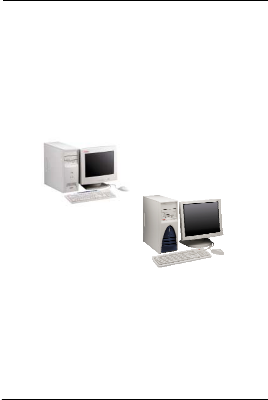
Technical Reference Guide
Compaq Deskpro EXS and Workstation 300 Personal Computers
Featuring the Intel Pentium 4 Processor
First Edition - December 2000
2-1
Chapter 2
SYSTEM OVERVIEW
2. Chapter 2 SYSTEM OVERVIEW
2.1 INTRODUCTION
Compaq Deskpro Personal Computers (Figure 2-1) featuring the Intel Pentium 4 processor provide
very high performance for advanced e-business and multimedia applications. This guide covers
Compaq Deskpro EXS Minitower and the Compaq Deskpro Workstation 300 models that feature
the Intel Pentium 4 processor and the Intel 850 chipset.
Figure 2–1. Compaq Deskpro Personal Computers with Monitors
This chapter includes the following topics:
♦ Features and options (2.2) page 2-2
♦ Mechanical design (2.3) page 2-4
♦ System architecture (2.4) page 2-8
♦ Specifications (2.5) page 2-13
Compaq Deskpro Workstation 300
Compaq Deskpro EXS Minitower

Chapter 2 System Overview
Compaq Deskpro EXS and Workstation 300 Personal Computers
Featuring the Intel Pentium 4 Processor
First Edition – December 2000
2-2
2.2 FEATURES AND OPTIONS
This section describes the standard features and available options.
2.2.1 STANDARD FEATURES
The following standard features are included on all models:
♦ Intel Pentium 4 processor in PPGA423 package
♦ Intel 850 chipset
♦ Dual-channel Direct Rambus system memory
♦ Five 33-MHz/32-bit PCI slots
♦ One AGP slot
♦ Embedded Sound Blaster 128 PCI audio
♦ 3.5 inch, 1.44-MB diskette drive
♦ 48x Max CD-ROM drive
♦ IDE controllers with UATA/100 mode support
♦ Hard drive fault prediction
♦ One parallel, two serial, and four USB ports
♦ APM 1.2 power management support
♦ Plug ’n Play compatible (with ESCD support)
♦ Intelligent Manageability support
♦ Energy Star compliant
♦ Security features including:
• Flash ROM Boot Block
• Diskette drive disable, boot disable, write protect
• Power-on password
• Administrator password
• Serial/parallel port disable
♦ PS/2 Compaq Easy-Access keyboard w/Windows support
♦ PS/2 Compaq Scroll Mouse
Table 2-1 shows the differences in standard features between the Deskpros:
Table 2-1. Standard Feature Difference Matrix
Table 2-1.
Standard Feature Difference Matrix
Deskpro EXS Deskpro Workstation 300
Form Factor Minitower Convertible Minitower
Standard Memory Type Installed Non-ECC ECC
Communication device 10/100 NIC & V.90 56K Modem 10/100 NIC only
Mass Storage:
Interface Type
Drive Type UATA100
20- or 40-MB Ultra 160 SCSI / UATA100
18 GB / 20 GB
Standard AGP Graphics Card NVIDIA GeForce2 GTS NVIDIA TNT2 Pro,
NVIDIA Quadro2 MXR,
ELSA Gloria II, or
Matrox Millennium G450

Technical Reference Guide
Compaq Deskpro EXS and Workstation 300 Personal Computers
Featuring the Intel Pentium 4 Processor
First Edition - December 2000
2-3
2.2.2 OPTIONS
The following items are available as options for all models and may be included in the standard
configuration of some models:
♦ System Memory: PC800 64-MB RIMM (non-ECC, ECC)
PC800 128-MB RIMM (non-ECC, ECC)
PC800 256-MB RIMM (non-ECC, ECC)
♦ Hard drives/controllers: 20-, 40-GB UATA/100 hard drive
Ultra 160 SCSI Controller
18-GB SCSI hard drive
♦ Removeable media drives: 8x/4x/32x CD-RW drive
10x/40x Max DVD-ROM drive
LS-120 Super Disk drive
PCI DXR DVD Decoder kit
♦ Graphics Monitors: Compaq P700 17” CRT
Compaq P900 19” CRT
Compaq P1100 21” CRT
Compaq TFT5010 15” Flat Panel
Compaq TFT8020 18” Flat Panel
♦ Audio Accessories: PS115 Speakers
PS330 Speakers
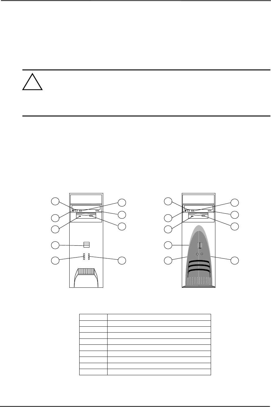
Chapter 2 System Overview
Compaq Deskpro EXS and Workstation 300 Personal Computers
Featuring the Intel Pentium 4 Processor
First Edition – December 2000
2-4
2.3 MECHANICAL DESIGN
The following subsections describe the mechanical (physical) aspects of the covered Compaq
Deskpro models.
CAUTION: Voltages are present within the system unit whenever the unit is plugged
into a live AC outlet, regardless of the “Power On” condition. Always disconnect the
power cable from the power outlet and/or from the system unit before handling the
system unit in any way. The following information is intended primarily for
identification purposes only. Before servicing these systems refer to the applicable
Maintenance And Service Guide and/or Service Reference Guide.
2.3.1 CABINET LAYOUTS
2.3.1.1 Front Views
Figure 2-2 shows the front cabinet layouts of the controls and indicators.
Item Description
1 Power button
2 Power LED
3 Hard drive activity LED
4 CD-ROM drive headphone jack
5 CD-ROM drive volume control
6 CD-ROM drive activity LED
7 CD-ROM drive door open/close button
8 1.44-MB diskette drive activity LED
9 1.44-MB diskette drive eject button
Figure 2–2. Front Cabinet Views
!
Desk
p
ro Workstation 300
23
1
47
8
5
9
6
Desk
p
ro EXS
23
1
47
8
5
9
6
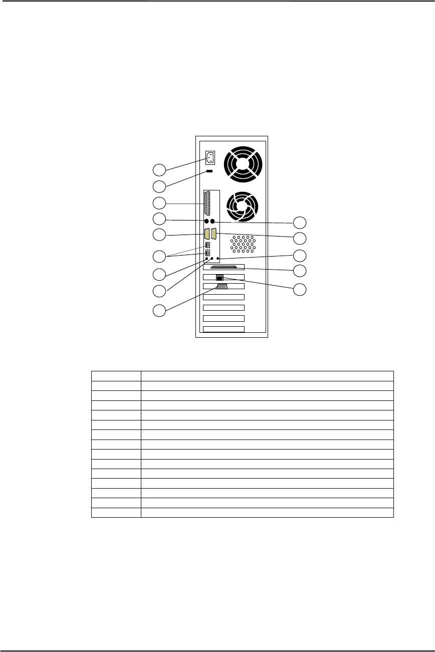
Technical Reference Guide
Compaq Deskpro EXS and Workstation 300 Personal Computers
Featuring the Intel Pentium 4 Processor
First Edition - December 2000
2-5
2.3.1.2 Rear View
Figure 2-3 shows the rear cabinet layout of the controls and connectors.
Item Description
1 AC line In Connector (115V/230V)
2 Line voltage switch
3 Parallel I/F connector
4 PS/2 keyboard connector
5 PS/2 mouse connector
6 Serial port A connector
7 Serial port B connector
8 USB ports (4)
9 Microphone In audio jack
10 Headphone/Line Out audio jack
11 Line In audio jack
12 Ultra SCSI connector (some Workstation models only)
13 Network I/F connector
14 Graphics (RGB) monitor connector
Figure 2–3. Rear Cabinet View
6
10
8
1
4
2
3
12
11
5
7
9
13
14
Chapter 2 System Overview
Compaq Deskpro EXS and Workstation 300 Personal Computers
Featuring the Intel Pentium 4 Processor
First Edition – December 2000
2-6
2.3.2 CHASSIS LAYOUT
For detailed information on servicing the chassis refer to the multimedia training CD-ROM and/or
the maintenance and service guide for these systems.
Figure 2-4 shows the layout for the system in a minitower configuration. This chassis provides:
♦ Three 5 ¼-inch drive bays and two 3 ½-inch drive bays
♦ Easy access to expansion slots and all socketed system board components.
♦ Space for either a µATX- or full ATX-type system board.
NOTE: [1] May be populated with a V.90 56K modem in Deskpro EXS models.
May be populated with an Ultra 160 SCSI adapter in select Workstaton 300 models.
Figure 2–4. Chassis Layout, Left Side View
Front
Back
Power Supply
Drive Bays
System Board
Chassis Fan/
Air Baffle
PCI Slot 1 [1]
PCI Slot 2 [1]
Graphics Card in AGP Slot
PCI Slot 3
PCI Slot 4
PCI Slot 5
Processor
Speaker
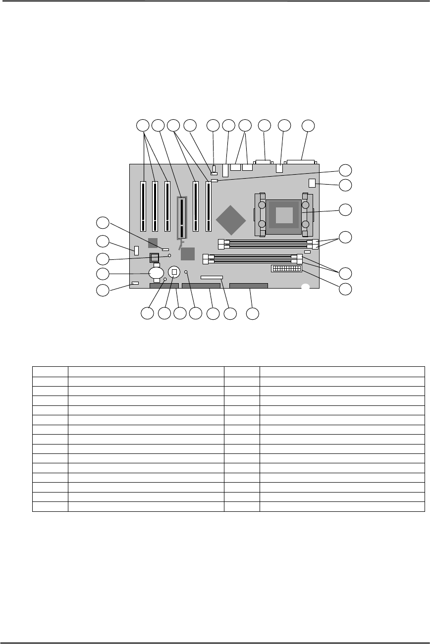
Technical Reference Guide
Compaq Deskpro EXS and Workstation 300 Personal Computers
Featuring the Intel Pentium 4 Processor
First Edition - December 2000
2-7
2.3.3 BOARD LAYOUT
These systems use an ATX-type system board. Figure 2-5 shows the location of sockets,
connectors, headers, switches, jumpers, and LEDs.
Item Description Item Description
1 PCI expansion bus slot connectors 15 Power supply connector
2 AGP slot connector 16 Secondary IDE connector
3 Auxiliary audio input header 17 Power/LED connector [1]
4 Chassis fan header 18 Primary IDE connector
5 Line In, HP/Line Out, Mic In connectors 19 Power supply on / 5V Aux power LED
6 USB ports (4) 20 Diskette drive connector
7 Top: Serial port B; Bottom: serial port A 21 CMOS clear button
8 Top: mouse connector, Bot.: Kybd conn. 22 Power button LED
9 Parallel port connector 23 Speaker connector
10 CD audio input header 24 Battery
11 CPU power connector 25 3.3V aux power LED
12 Processor socket 26 AOL/SOS header
13 Channel B RIMM sockets 3, 4 27 Password clear jumper [2]
14 Channel A RIMM sockets 1, 2 -- --
NOTE: [1] Connector for power button, Power/HD LEDs, and SCSI HD LEDs.
[2] Jumper installed, password enabled. Jumper removed, password cleared.
Figure 2–5. System Board Layout
System Board
(PCA# 010821)
6
2
192021
1
10
18 17
14
16
3
24
9
5
11
1 7 8
13
4
25
26
27
23 15
22
12

Chapter 2 System Overview
Compaq Deskpro EXS and Workstation 300 Personal Computers
Featuring the Intel Pentium 4 Processor
First Edition – December 2000
2-8
2.4 SYSTEM ARCHITECTURE
These systems feature architecture based on the Intel Pentium 4 processor and the Intel 850 chipset
(Figure 2-6). These components are designed to compliment each other to provide very high
desktop/minitower performance. Key technical highlights of this architecture include:
♦ 1.4 or 1.5-GHz Pentium 4 processor
♦ Quad-pumped Front Side Bus (FSB) for 400-MHz performance
♦ Dual-channel RDRAM controller supporting up to four PC800 RIMMs
♦ Two IDE controllers supporting two UATA-100 hard drives each
♦ Sound Blaster 128 audio subsystem
♦ Five 33-MHz/32-bit PCI slots
♦ AGP 4X slot (1.5-volt support only)
♦ One parallel port
♦ Two serial ports
♦ Four USB ports
♦ PS/2 mouse and keyboard interfaces
The Pentium 4 processor represents Intel’s latest IA-32 microprocessor design and features a
hyper-pipelined, rapid-execution engine for improved system responsiveness and higher execution
throughput. Internet and multimedia performance is improved further with additional streaming
SIMD extensions (SSE2) designed to expedite video, speech, encryption, and photo processing
tasks.
The 3.2 GB/s throughput of the FSB matches that of the dual-channel RDRAM used for system
memory, reducing latency and providing high, balanced performance. The 82850 Memory
Controller Hub (MCH) includes an AGP 4X interface supporting a 1.5-VDC graphics card in the
AGP slot.
The 82801BA I/O Controller Hub (ICH2) and the LPC47B357 I/O Controller components provide
most of the input/output functions listed previously. These systems also include an AGP 4X
graphics card in the AGP slot and an Intel PRO/100+ Management Adapter (NIC) card in a PCI
slot. Some models may also include a modem card and a SCSI host adapter installed in PCI slots.
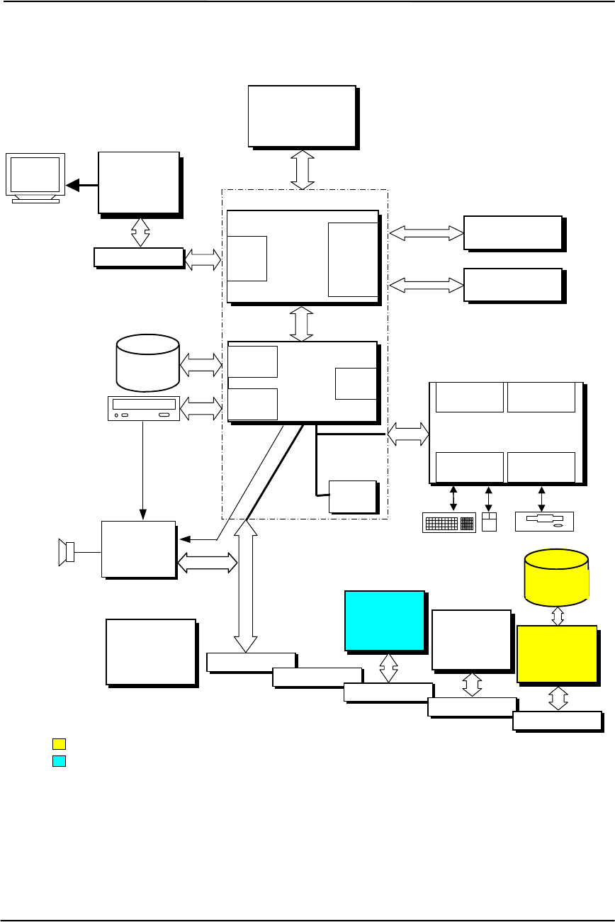
Technical Reference Guide
Compaq Deskpro EXS and Workstation 300 Personal Computers
Featuring the Intel Pentium 4 Processor
First Edition - December 2000
2-9
Figure 2–6. System Architecture, Block diagram
82801BA
ICH2
Pri. IDE
I/F USB
I/F (4)
Power
Supply
82802
FWH
Sec. IDE
I/F
LPC47B357 I/O Controller
Serial
I/F (2) Parallel
I/F
Keyboard/
Mouse I/F Diskette
I/F
33-MHz
32-Bit PCI Bus
UATA/100
Hard Drive
850 Chipset
LPC
Bus
Hub Link
Bus
PCI Slot 5
Pentium 4
Processor
82850
MCH
400- MHz FSB
RDRAM
Cntlr.
Beep
Audio
CD
Audio
AGP
4X
I/F
RGB Graphics
Controller
Card
Audio
Subsystem
Channel A
RDRAM Bus PC800
RIMM Pair(s)
PCI Slot 4
PCI Slot 3
PCI Slot 2
AGP Slot Channel B
RDRAM Bus PC800
RIMM Pair(s)
V.90
56K
PCI
Modem Card
PCI Slot 1
Intel
PRO/100+
Mgmt.
Adapter Card
Adaptec
29160N
SCSI
Ada
p
ter Card
SCSI
Hard Drive
Some Deskpro Workstation 300 models.
Some Deskpro EXS models.
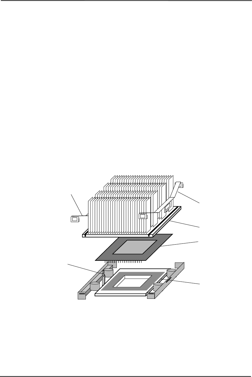
Chapter 2 System Overview
Compaq Deskpro EXS and Workstation 300 Personal Computers
Featuring the Intel Pentium 4 Processor
First Edition – December 2000
2-10
2.4.1 PENTIUM 4 PROCESSOR
These systems feature the Intel Pentium 4 processor featuring Intel’s NetBurst Micro-
Architecture. This processor is backward-compatible with software written for the Pentium III/II,
Pentium MMX, Pentium Pro, Pentium, and x86 microprocessors.
Key features of the Pentium 4 processor include:
♦ Hyper-Pipelined Technology for higher performance
♦ Rapid Execution Engine with increased throughput and reduced latency
♦ Quad-pumped Front Side Bus (FSB) for balanced performance with RDRAM
♦ Execution Trace Cache for more efficient branch-handling
♦ Improved dynamic execution for higher efficiency
♦ Additional Streaming SIMD Extensions (SSE2) for increased video, audio, and speech
processing
♦ On-die (full speed) 256-KB ECC second-level cache
These systems employ a PGA423 zero-insertion-force (ZIF) socket designed for mounting a “Flip-
Chip” (FC-PGA423) processor package (Figure 2-7).
Figure 2–7. Processor Assembly And Mounting
The PGA423 socket allows easy changing/upgrading of the processor. Raising the Lock/Unlock
handle of the socket in the vertical position allows the processor package to be removed or inserted
into the socket. Lowering the Lock/Unlock handle in the down (horizontal) position locks the
processor package in place. The heat sink is placed on top of the processor and held in place by
two retaining clips.
Heat Sink
FC-PGA423
Package
PGA423
Socket
Heat Sink
Retaining Clip
Lock/Unlock
Handle
(Shown in unlock position)
Heat Sink
Retaining Clip

Technical Reference Guide
Compaq Deskpro EXS and Workstation 300 Personal Computers
Featuring the Intel Pentium 4 Processor
First Edition - December 2000
2-11
2.4.2 CHIPSET
The chipset consists of a Memory Controller Hub (MCH), an I/O Controller Hub (ICH), and a
FirmWare Hub (FWH). Table 2-2 lists the integrated functions provided by the two types of
chipsets used in these systems.
Table 2-2. Chipset Comparison
Table 2-2.
Chipset Comparison
Chipset Component Function
850 82850 MCH AGP 4X interface
Dual-channel RDRAM controller supporting up to 4 PC800 RIMMs
400-MHz FSB
82801BA ICH2 PCI bus I/F
LPC bus I/F
SMBus I/F
IDE I/F with UATA/100 support
AC ’97 controller
RTC/CMOS
IRQ controller
Power management logic
USB I/F (4)
8259 and I/O APIC interrupt processing
82802 FWH Loaded with Compaq BIOS
2.4.3 SUPPORT COMPONENTS
Input/output functions not provided by the chipset are handled by other support components. Table
2-3 shows the functions provided by the support components.
Table 2-3. Support Component Functions
Table 2-3.
Support Component Functions
Component Name Function
LPC47B357 7 I/O Controller Keyboard and pointing device I/F
Diskette I/F
Serial I/F (COM1and COM2)
Parallel I/F (LPT1, LPT2, or LPT3)
AGP, PCI reset generation
ISA serial IRQ converter
Power button and LED control logic
GPIO ports
ES1373 PCI audio controller
CS4297A Audio Codec Audio mixer
Digital-to-analog converter
Analog-to-digital converter
Analog I/O

Chapter 2 System Overview
Compaq Deskpro EXS and Workstation 300 Personal Computers
Featuring the Intel Pentium 4 Processor
First Edition – December 2000
2-12
2.4.4 SYSTEM MEMORY
These systems feature a dual-channel Direct Rambus (RDRAM) architecture. Capable of a peak
data throughput of 3.2 GB/sec., this high-performance memory design represents a new generation
of memory subsystems that can keep pace with ever-increasing processor performance. These
systems each provide a total of four RIMM sockets, all of which will be populated with either
PC800 RDRAM memory modules (RIMMs) or continuity modules (CRIMMs). Up to two
gigabytes of memory may be installed.
Compaq Deskpro EXS systems are shipped with non-ECC PC800 RIMMs. Compaq Deskpro
Workstation 300 systems are shipped with ECC PC800 RIMMs. Both systems support ECC and
non-ECC RIMMs.
2.4.5 MASS STORAGE
All models include a 3.5 inch 1.44-MB diskette drive installed as drive A. Most models also
include a CD-ROM drive. The Deskpro EXS and some Deskpro Workstation 300 models will
include a UATA100 (EIDE) hard drive while select Deskpro Workstation 300 models will include
an Ultra 160 SCSI controller (PCI) card and SCSI hard drive. Standard hard drives feature Drive
Protection System (DPS) support, which uses industry-standard function ATAPI-5 to check drive
integrity. Standard drives also use SMART III technology that tests drive data during periods of
drive inactivity for corruption.
2.4.6 SERIAL, PARALLEL INTERFACES
All models include two serial ports and a parallel port accessible at the rear of the chassis. Each
serial port is RS-232-C/16550-compatible and supports standard baud rates up to 115,200 as well
as high-speed baud rates of 230K and 460K, and uses a DB-9 connector. The parallel interface is
Enhanced Parallel Port (EPP1.9) and Enhanced Capability Port (ECP) compatible, and supports
bi-directional data transfers through a DB-25 connector.
2.4.7 UNIVERSAL SERIAL BUS INTERFACE
All models feature four Universal Serial Bus (USB) ports that provide a 12Mb/s interface for
peripherals. The USB provides hot plugging/unplugging (Plug ’n Play) functionality.

Technical Reference Guide
Compaq Deskpro EXS and Workstation 300 Personal Computers
Featuring the Intel Pentium 4 Processor
First Edition - December 2000
2-13
2.4.8 GRAPHICS SUBSYSTEM
Each of these systems provides an AGP slot that accommodates a Type 1 or Type 2 AGP graphics
adapter (1.5-V only).
Table 2-4 lists the key features of the types of graphics adapters available as standard in these
systems:
Table 2-4. Standard AGP Graphics Card Comparison
Table 2-4.
Standard AGP Graphics Card Comparison
NVIDIA
GeForce2 GTS NVIDIA
TNT2 PRO NVIDIA
Quadro2 MXR ELSA
GLoria II
Matrox
Millennium
G450
Std. Config. In EXS Wkstn. 300 Wkstn. 300 Wkstn. 300 Wkstn. 300
Recommended
for: Hi 2D,
Entry 3D Hi 2D,
Entry 3D Hi 2D,
Entry 3D Hi 2D,
Mid 3D Multi-monitor
Hi 2D
Bus Type AGP 4X AGP 2X/4X AGP 2X/4X AGP 2X/4X AGP 2X/4X
Mem. Amount 32 MB 16 MB 32 MB 64 MB 32 MB
Mem. Type SDRAM SGRAM SDRAM SDRAM DDR SDRAM
DAC Speed 350 MHz 300 MHz 350 MHz 350 MHz
Max. 2D Res. @
# of colors 2048x1536
@ 16.7M 1920x1200
@ 16.7M 1920x1200
@ 16.7M 2048x1536
@ 16.7M 2048x768
@ 65K
Software
Compatibility Quick Draw,
DCI/DirectX,
Direct Draw,
3D OGL,
MPEG 1/2
Quick Draw,
DCI/DirectX,
Direct Draw,
Direct Show,
MPEG 1/2,
Indeo
Quick Draw,
DCI/DirectX,
Direct Draw,
Direct Show,
MPEG 1/2,
Indeo
Quick Draw,
DCI/DirectX,
Direct Draw,
ActiveX,
MPEG 1/2,
OpenGL
Quick Draw,
DCI/DirectX,
Direct Draw,
MPEG 1/2,
OpenGL,
Direct 3D
Special
Features/
Accelerators
3ROP BitBLT,
Line Draw,
Color Expan.
Triangle Eng,
Anti-aliasing,
HDTV proc.,
FS Anti-
aliasing,
32b color &
stencil,
Alpha planes
Transparent
BLT,
Stretch BLT,
Polylines,
Polygons,
Fills,
32b render,
24b Z-buffer, 8b
stencil,
Anisotropic
filtering,
128b TnT
Archit.
Shading
rasterizer,
Digital vibrance
control,
32b render,
24b Z-buffer, 8b
stencil,
Anisotropic
filtering,
Twin View arch.
supporting
2-head Win. &
2-head clone,
DVD support,
24b dbl-
buffered color
planes,
8b stencil,
24b Z-buffer,
stereo support,
3ROP BitBLT,
Dual RAMDAC,
Flat & Gouraud
shading,
Anisotropic
filtering,
Perspective
Texture,
Specular
highlighting,
32b z-buffer,
2-head zoom,
2-head clone,
2-head TV,
DVD max mode
Aux. I/O VESA I/F VESA I/F VESA I/F VESA I/F VESA I/F
Outputs 1 RGB 1 RGB 1 RGB, 1 DVI 1 RGB 2 RGB
NOTE:

Chapter 2 System Overview
Compaq Deskpro EXS and Workstation 300 Personal Computers
Featuring the Intel Pentium 4 Processor
First Edition – December 2000
2-14
2.4.9 AUDIO SUBSYSTEM
All models feature an embedded Sound Blaster 128 PCI audio system using the AC’97 ver. 2.1
specification-based design. The subsystem features a Creative Labs, Inc. ES1373 audio controller
and a Cirrus Logic CS4297A audio codec. The output of the audio codec is applied to a 3-watt
amplifier that drives the chassis’ internal speaker. Standard microphone and line input jacks are
provided as well as a tri-purpose headphone/line/digital output jack that allows the use of
headphones or a pair of powered speakers (optional). The output jack also provides a digital audio
output signal using the Sony/Philips Digital Interface (SPDIF) format (officially known as IEC-
958).
2.5 SPECIFICATIONS
This section includes the environmental, electrical, and physical specifications for the Compaq
Deskpro EXS and Workstation 300 Series Personal Computers. Where provided, metric statistics
are given in parenthesis. All specifications subject to change without notice.
Table 2-5. Environmental Specifications
Table 2-5.
Environmental Specifications (Factory Configuration)
Parameter Operating Nonoperating
Ambient Air Temperature 50o to 95o F (10o to 35o C, max. rate
of change < 10°C/Hr) -24o to 140o F (-30o to 60o C, max.
rate of change < 20°C/Hr )
Shock (w/o damage) 5 Gs [1] 20 Gs [1]
Vibration 0.000215 G2/Hz, 10-300 Hz 0.0005 G2/Hz, 10-500 Hz
Humidity 10-90% Rh @ 28o C max.
wet bulb temperature 5-95% Rh @ 38.7o C max.
wet bulb temperature
Maximum Altitude 10,000 ft (3048 m) [2] 30,000 ft (9,144 m) [2]
NOTE: [1] Peak input acceleration during an 11 ms half-sine shock pulse.
[2] Maximum rate of change: 1500 ft/min.
Table 2-6. Electrical Specifications
Table 2-6.
Electrical Specifications
Parameter U.S. International
Input Line Voltage:
Nominal:
Maximum: 110 - 127 VAC
90 - 132 VAC 200 - 240 VAC
180 - 264 VAC
Input Line Frequency Range:
Nominal:
Maximum: 50 - 60 Hz
47 - 63 Hz 50 - 60 Hz
47 - 63 Hz
Power Supply:
Maximum Continuous Power
Maximum Line Current Draw watts
A watts
A

Technical Reference Guide
Compaq Deskpro EXS and Workstation 300 Personal Computers
Featuring the Intel Pentium 4 Processor
First Edition - December 2000
2-15
Table 2-7. Physical Specifications
Table 2-7.
Physical Specifications
Parameter Desktop Configuration Minitower Configuration
Height 6.60 in (16.76 cm) 17.65 in (44.83 cm)
Width 17.65 in (44.83 cm) 6.60 in (16.76 cm)
Depth 17.11 in (43.46 cm) 17.11 in (43.46 cm)
Weight (nom.) [1] 26 lb (11.8 kg) 26 lb (11.8 kg)
Maximum Supported Weight [2] 100 N/A
NOTES: [1] System weight may vary depending on installed drives/peripherals.
[2] Assumes reasonable article(s) such as a display monitor and/or another system unit.
Table 2-8. Diskette Drive Specifications
Table 2-8.
Diskette Drive Specifications
(Compaq SP# 179161-001)
Parameter Measurement
Media Type 3.5 in 1.44 MB/720 KB diskette
Height 1/3 bay (1 in)
Bytes per Sector 512
Sectors per Track:
High Density
Low Density 18
9
Tracks per Side:
High Density
Low Density 80
80
Read/Write Heads 2
Average Access Time:
Track-to-Track (high/low)
Average (high/low)
Settling Time
Latency Average
3 ms/6 ms
94 ms/173ms
15 ms
100 ms

Chapter 2 System Overview
Compaq Deskpro EXS and Workstation 300 Personal Computers
Featuring the Intel Pentium 4 Processor
First Edition – December 2000
2-16
Table 2-9. 48x CD-ROM Drive Specifications
Table 2-9.
48x CD-ROM Drive Specifications
(SP# 187217-B21)
Parameter Measurement
Interface Type IDE
Transfer Rate:
Max. Sustained
Burst 4800 KB/s
16.6 MB/s
Media Type Mode 1,2, Mixed Mode, CD-DA,
Photo CD, Cdi, CD-XA
Capacity:
Mode 1, 12 cm
Mode 2, 12 cm
8 cm
550 MB
640 MB
180 MB
Center Hole Diameter 15 mm
Disc Diameter 8/12 cm
Disc Thickness 1.2 mm
Track Pitch 1.6 um
Laser
Beam Divergence
Output Power
Type
Wave Length
53.5 +/- 1.5 °
53.6 0.14 mW
GaAs
790 +/- 25 nm
Average Access Time:
Random
Full Stroke <100 ms
<150 ms
Audio Output Level 0.7 Vrms
Cache Buffer 128 KB
Table 2-10. Hard Drive Specifications
Table 2-10.
Hard Drive Specifications
Parameter 18.0 GB 20.0 GB 40.0 GB
Drive Size 3.5” 3.5” 5.25”
Interface Ultra 160 SCSI UATA/100 UATA/100
Drive Protection System Support? Yes Yes Yes
Transfer Rate (max) 160 MB/s 100 MB/s 100 MB/s
Typical Seek Time (w/settling) [1]
Single Track
Average
Full Stroke
1.7 ms
8.5 ms
15 ms
2.0 ms
9.5 ms
21 ms
1.0 ms
9.0 ms
20 ms
Disk Format (logical):
# of Cylinders
# of Data Heads
# of Sectors per Track
16383
16
63
16383
16
63
16383
16
63
Rotation Speed 10,000 RPM 7200 RPM 7200 RPM
Drive Fault Prediction SMART III SMART III SMART III
NOTE: Actual times may vary depending on specific drive installed.
All EMEA units feature Quiet Drives.
[1] Operates at 66 MB/s in these systems.
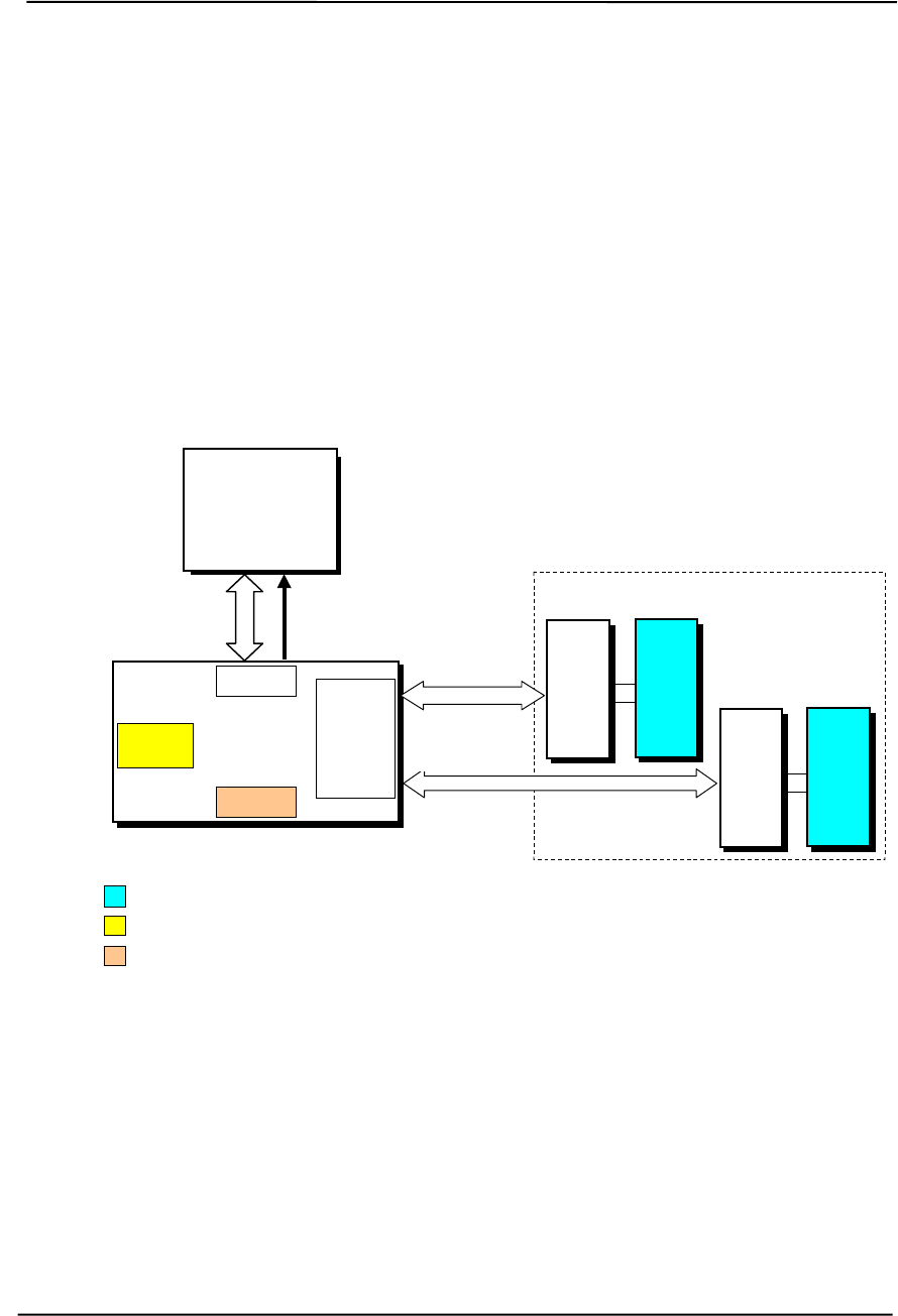
Technical Reference Guide
Compaq Deskpro EXS and Workstation 300 Personal Computers
Featuring the Intel Pentium 4 Processor
First Edition - December 2000
3-1
Chapter 3
PROCESSOR/
MEMORY SUBSYSTEM
3. Chapter 3 PROCESSOR/MEMORY SUBSYSTEM
3.1 INTRODUCTION
This chapter describes the processor/memory subsystem of Compaq Deskpro Personal Computers
featuring the Pentium 4 processor. These systems feature the Pentium 4 processor and the 850
chipset (Figure 3-1). The 82850 MCH component of the 850 chipset supports two Direct Rambus
channels, each channel accommodating one or two RIMMs.
Figure 3–1. Processor/Memory Subsystem Architecture
This chapter includes the following topics:
♦ Pentium 4 processor [3.2] page 3-2
♦ Memory subsystem [3.3] page 3-5
♦ Subsystem configuration {3.4] page 3-8
Pentium 4
Processor
400-MHz
64-Bit FSB Cntl
Rambus
Channel 1 /16
System Memory
RIMM
In
Socket
XMM1 XMM2
RIMM
Socket
82850
MCH
FSB I/F
AGP
I/F
Rambus
Cntlr.
Hub I/F
Will be populated with optional RIMM or CRIMM
Covered in Chapter 6
Covered in Chapter 4
RIMM
In
Socket
XMM3 XMM4
RIMM
Socket
Rambus
Channel 2 /16

Chapter 3 Processor/Memory Subsystem
Compaq Deskpro EXS and Workstation 300 Personal Computers
Featuring the Intel Pentium 4 Processor
First Edition - December 2000
3-2
3.2 PENTIUM 4 PROCESSOR
These systems each feature an Intel Pentium 4 processor in a FC-PGA423 package mounted with a
passive heat sink in a PGA423 (W-type) zero-insertion force socket. The mounting socket allows
the processor to be easily changed for servicing and/or upgrading.
3.2.1 PROCESSOR OVERVIEW
The 1.4-/1.5-GHz Intel Pentium 4 processor represents the latest generation of Intel’s IA32-class
of processors. Featuring Intel’s NetBurst architecture, the Pentium 4 processor is designed for
intensive multimedia and internet applications of today and the future while maintaining
compatibility with software written for earlier (Pentium III, Pentium II, Pentium, Celeron, and x86)
microprocessors. Key features of the Pentium 4 processor include:
♦ Hyper-Pipelined Technology – The main processing loop has twice the depth (20 stages) of
the Pentium III allowing for increased processing frequencies.
♦ Execution Trace Cache – A new feature supporting the branch prediction mechanism, the
trace cache stores translated sequences of branching micro-operations (µops) and is checked
when suspected re-occurring branches are detected in the main processing loop. This feature
allows instruction decoding to be removed from the main processing loop.
♦ Rapid Execution Engine – Arithmetic Logic Units (ALUs) run at twice (2x) processing
frequency for higher throughput and reduced latency.
♦ 256-KB Advanced transfer L2 cache – Using 32-byte-wide interface at processing speed, the
L2 cache can provide 48 GB/s perrformance (3x over the Pentium III)
♦ Advanced dynamic execution – Using a larger (4K) branch target buffer and improved
prediction algorithm, branch mis-predictions are reduced by an average of 33 % over the
Pentium III.
♦ Enhanced Floating Point Processor - With 128-bit integer processing and deeper pipelining
the Pentium 4’s FPU provides a 2x performance boost over the Pentium III.
♦ Additional Streaming SIMD extensions (SSE2) – In addition to the SSE support provided by
previous Pentium processors, the Pentium 4 processor includes an additional 144 MMX
instructions, further enhancing:
• Streaming video/audio processing
• Photo/video editing
• Speech recognition
• 3D processing
• Encryption processing
♦ Quad-pumped Front Side Bus (FSB) – The FSB uses a 100-MHz clock for qualifying the
buses’ control signals. However, address information is transferred using a 200-MHz strobe
while data is transferred with a 400-MHz strobe, providing a maximum data transfer rate of
3.2 GB/s. This is a 3x boost over a Pentium III with a 133-MHz FSB. The 3.2 GB/s peak
transfer rate of the FSB balances the 3.2 GB/s maximum transfer capability of the dual-
channel Direct Rambus system memory.

Technical Reference Guide
Compaq Deskpro EXS and Workstation 300 Personal Computers
Featuring the Intel Pentium 4 Processor
First Edition - December 2000
3-3
Figure 3-1 illustrates the internal architecture of the Pentium 4 processor.
Figure 3–2. Pentium 4 Processor Internal Architecture
The Pentium 4 increases processing speed with higher clock speeds made possible with hyper-
pipelined technology that can handle significantly more instructions at a time. Since branch mis-
predicts would result in serious performance hits with such a long pipeline, the Pentium 4 features
a branch prediction mechanism improved with the addition of an execution trace cache and a
refined prediction algorithm. The execution trace cache can store 12k micro-ops (decoded
instructions dealing with branching sequences) that are checked when re-occurring branches are
processed. Code that is not executed (bypassed) is no longer stored in the L1 cache as was the case
in the Pentium III.
The out-of-order core features Advanced Dynamic Execution, which provides a large window (126
instructions) for execution units to work with. A more accurate branch prediction algorithm, along
with a larger (4-KB) branch target buffer that stores more details on branch history results in a
33% reduction in branch mis-predictions over the Pentium III.
The L1 data cache features a low-latency design for minimum response to cache hits. The 256-KB
advanced transfer L2 cache features a 256-bit (32-byte) interface operating at processing speed.
The L2 cache of the 1.5 GHz Pentium 4 can therefore provide a transfer rate of 48 GB/s.
The combined improvements of the Pentium 4’s CPU core the rapid execution engine’s ALUs to
operate at twice the processing frequency to handle the steady stream of instructions.
The front side bus (FSB) of the Pentium 4 uses a 100-MHz clock but provides Quad-pumped data
transfers. While the Pentium III could transfer 8 bytes of data on a 133-MHz clock cycle the
Pentium 4 can transfer 32 bytes of data on a 100-MHz clock cycle for a throughput rate of 3.2
GB/s, balancing the performance of the dual-Rambus memory subsystem. Address information is
transferred at a 200-MHz rate.
ALU Speed: 2.8 GHz w/Pentium 4 @ 1.4 GHz
3.0 GHz w/Pentium 4 @ 1.5 GHz
Core Speed: 1.4 GHz w/Pentium 4 @ 1.4 GHz
1.5 GHz w/Pentium 4 @ 1.5 GHz
FSB Speed: 400 MHz (Data transfer rate)
Pentium 4 Processor
128-bit
Integer
FPU L1
Data
Cache
256-KB
8-Way
L2
Adv.
Transfer
Cache
FSB
I/F
Rapid Exe. Eng.
Branch
Prediction
CPU
ALUs
Execution
Trace Cache
Out-of-
Order Core

Chapter 3 Processor/Memory Subsystem
Compaq Deskpro EXS and Workstation 300 Personal Computers
Featuring the Intel Pentium 4 Processor
First Edition - December 2000
3-4
The Pentium 4 processor is software-compatible with Celeron, Pentium II, Pentium MMX,
Pentium, and x86 processors, but will require the latest versions of operating system software to
take advantage of the Streaming SIMD extensions (SSE2).
3.2.2 PROCESSOR UPGRADING
All units use the PGA423 ZIF mounting socket and ship with the Pentium 4 processor in a Flip-
Chip (FC-PGA423) package installed with a passive heat sink. The FC-PGA423 package consists
of the processor die mounted “upside down” on a PC board. This arrangement allows the heat sink
to come in direct contact with the processor die. The heat sink and attachment clip are specially
designed provide maximum heat transfer from the processor component.
CAUTION: Attachment of the heat sink to the processor is critical on these systems.
Improper attachment of the heat sink will likely result in a thermal condition.
Although the system is designed to detect thermal conditions and automatically shut
down, such a condition could still result in damage to the processor component. Refer to
the applicable Maintenance and Service Guide for processor installation instructions.
!
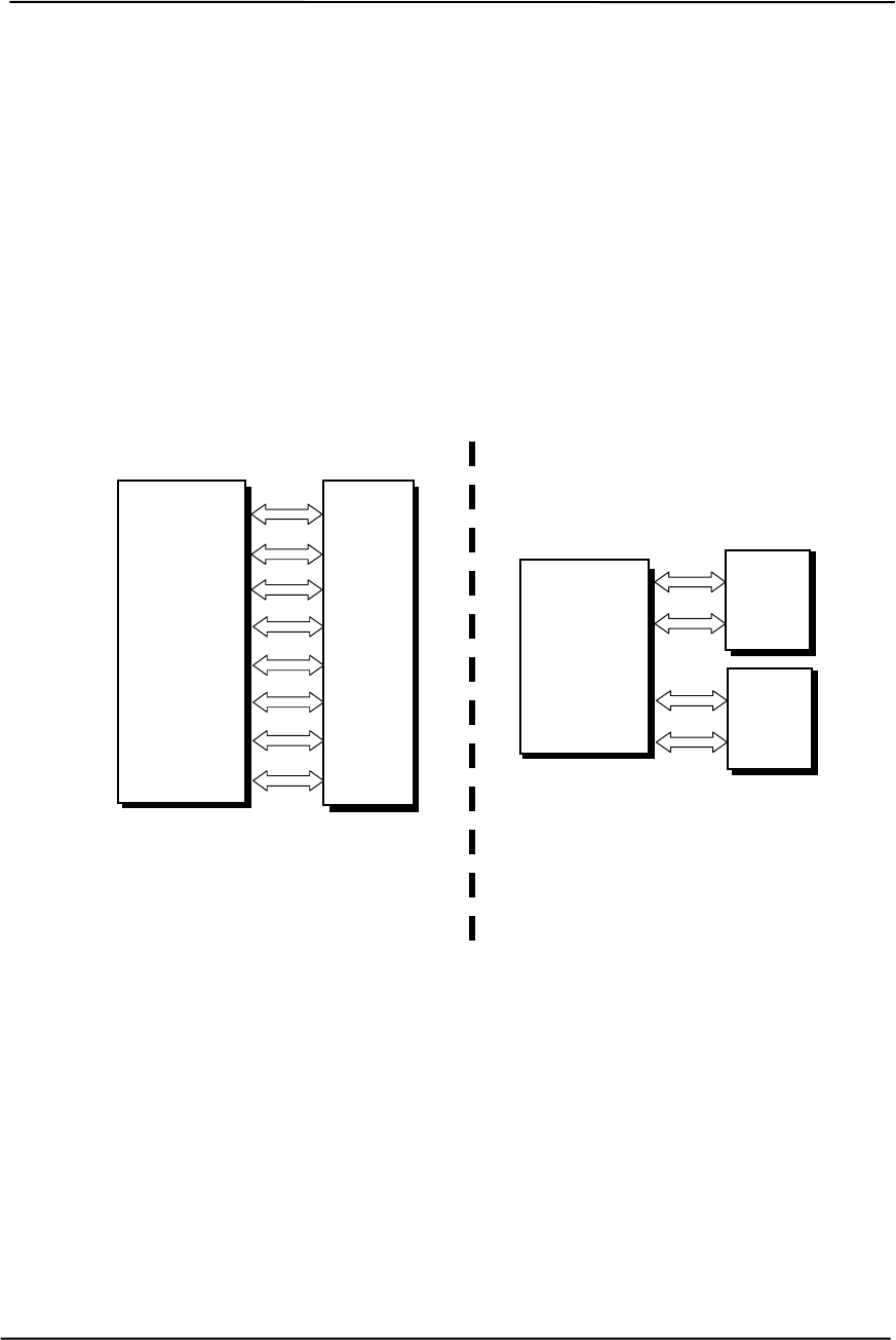
Technical Reference Guide
Compaq Deskpro EXS and Workstation 300 Personal Computers
Featuring the Intel Pentium 4 Processor
First Edition - December 2000
3-5
3.3 MEMORY SUBSYSTEM
The 82850 MCH features Direct Rambus technology and supports two Rambus channels, each
channel supporting up to two Rambus DRAM modules (RIMMs). Direct Rambus technology
provides a significant improvement in performance over DRAM/SDRAM memory designs and
allows the system memory to keep pace with increasing processor performance. Rambus
technology implements RDRAM devices accessed over a channel specifically designed for high
speed operations.
As shown in Figure 3-3, the conventional DRAM-based memory interface with a transfer rate of
66, 100, or 133 MHz increases bandwidth by widening the data bus. With the current top speed of
133 MHz, a 64-bit SDRAM interface achieves a maximum transfer rate of 1.0 GB/s.
Figure 3–3. SDRAM/RDRAM Bandwidth Comparison
Although a Rambus channel handles only two bytes per transfer, data is clocked on both the rising
and falling edges of the clock signal, allowing a 400-MHz clock to provide an effective speed of
800 MHz and resulting a transfer rate of 1.6 GB/s. Doubling the number of channels doubles the
throughput. These systems feature dual-channel RDRAM architecture that provides a maximum
transfer rate of 3.2 GB/s.
SDRAM
Memory
Controller
SDRAM Interface
64-bit Path
8 bytes @ 133 MHz = 1.0 GB/s
DIMM
Byte 0
Byte 1
Byte 2
Byte 3
Byte 4
Byte 5
Byte 6
Byte 7
RDRAM Interface (Dual Channel)
32-bit Path
4 bytes @ 400 MHz = 3.2 GB/s (see text)
RDRAM
Memory
Controller
Byte 0
Byte 1
Ch 1
RIMM
Byte 2
Byte 3
Ch 2
RIMM
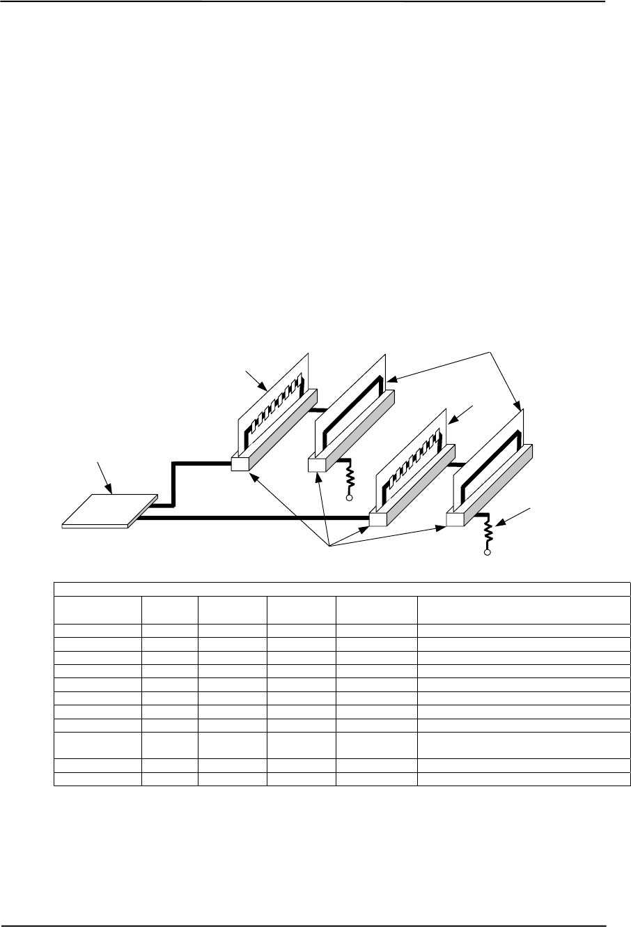
Chapter 3 Processor/Memory Subsystem
Compaq Deskpro EXS and Workstation 300 Personal Computers
Featuring the Intel Pentium 4 Processor
First Edition - December 2000
3-6
3.3.1 RAMBUS ATTRIBUTES
To ensure signal quality during high-speed memory transfers, the Rambus interface design departs
from previous memory interface designs in several key aspects (Figure 3-4). Rambus uses a daisy-
chained signal distribution system that requires that all memory sockets be populated with either a
RIMM or a continuity module (CRIMM) in order to maintain constant load impedance. Rambus
Signaling Levels (RSL) uses a 1.4-volt reference with a 0.8-volt swing between logic 0 at 1.8 V
and logic 1 at 1.0 V.
On these systems RIMMs (or CRIMMs) must be installed in pairs (one module for each channel).
A maximum of two gigabytes of memory may be installed using 512-MB RIMMs. These systems
ship with PC800 (400-MHz) RIMMs but will also accept PC700 or PC600 RIMMs. A mix of
ECC and non-ECC RIMMs may be installed, although all RIMMs must be ECC to realize ECC
benefits.
Rambus Signal Attributes (Each Channel)
Signal Name No. of
Lines Input/
Output [1] Signal
Level Impedance Function
ROW 2..0 3 O RSL 28 ohms Row address
COL 4..0 5 O RSL 28 ohms Column address
DQA 8..0 9 I/O RSL 28 ohms Data byte A (w/parity or ECC bit)
DQB 8..0 9 I/O RSL 28 ohms Data byte B (w/parity or ECC bit)
CFM, CFMN 2 O RSL [2] 28 ohms 400-MHz Clock-from-master for writes
CTM, CTMN 2 I RSL [2] 28 ohms 400-MHz Clock-to-master for reads
Vref 1 -- 1.4 V -- Reference voltage for RSL signals
SIO 1 I/O CMOS -- Serial I/F for initialization & pwr cntrl.
SCK 1 O CMOS 56 ohms SIO clock; 1 MHz for configuration,100
MHz for power management.
CMD 1 I/O CMOS 56 ohms Serial I/F config. & power control
Vdd -- 2.5 V -- Power for Rambus circuitry
NOTES: [1] Relative to the memory controller.
[2] Differential pair with Ep-p swing of 400 to 600 mV.
Figure 3–4. Rambus Channel Signal Distribution and Key Attributes
Bus Termination
RIMM Sockets
RIMM
MCH
RIMM or CRIMM (Shown)
Channel 1
Channel 2
RIMM
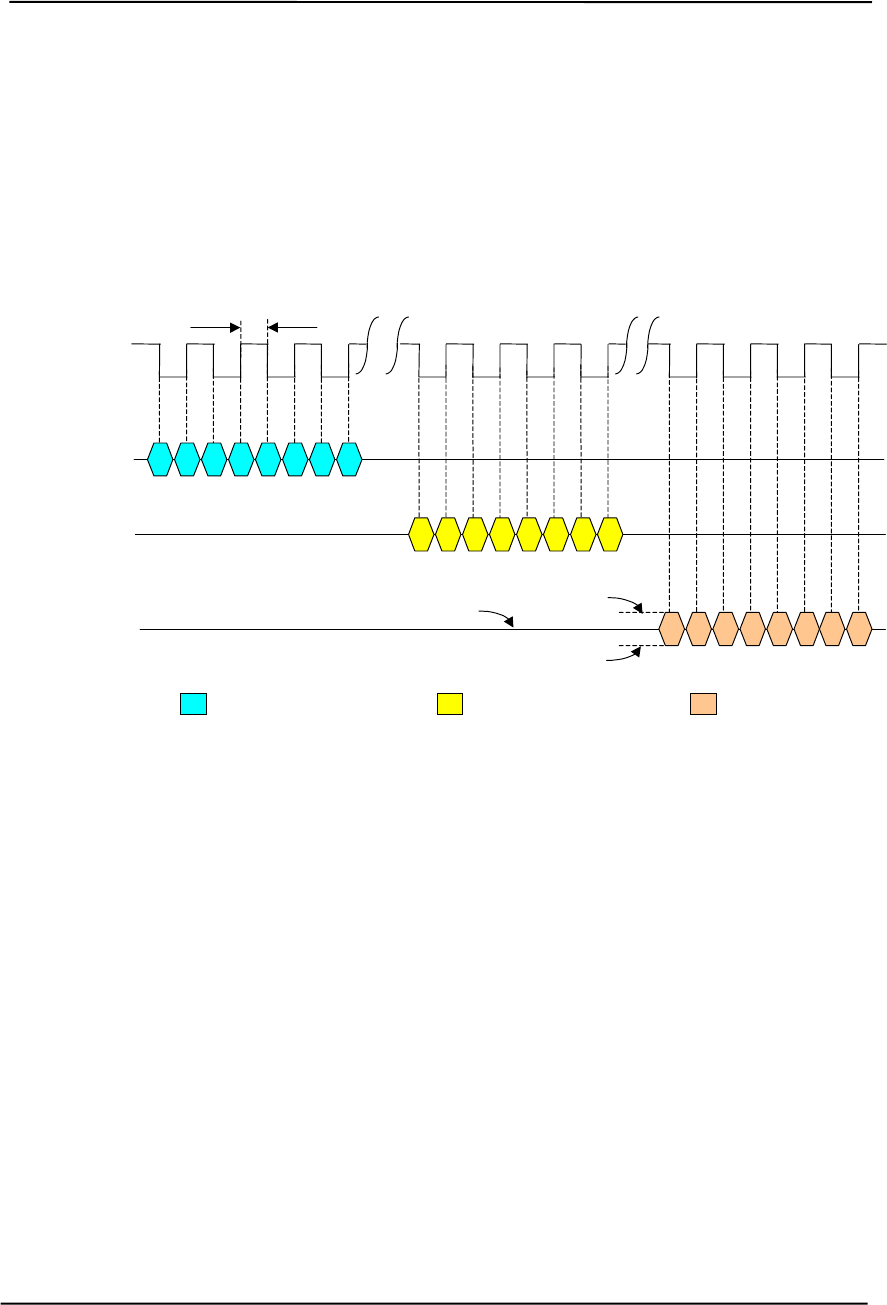
Technical Reference Guide
Compaq Deskpro EXS and Workstation 300 Personal Computers
Featuring the Intel Pentium 4 Processor
First Edition - December 2000
3-7
3.3.2 RAMBUS CHANNEL TRANSACTIONS
Transactions on the Rambus Channel involve packets of control (row or column) bits and packets
of data bits. Each packet consists of eight segments, with even segments transferred on falling
clock edges and odd segments transferred on rising clock edges. A typical operation consists of the
memory controller sending out a 24-bit row packet followed by a 40-bit column packet and then
the 144-bit (128-bit for non-ECC) data packet being either written to or read from RDRAM
(Figure 3-5).
NOTE: [1] Tn = 1.25 ns @ 400 MHz (PC800)
= 1.42 ns @ 350 MHz (PC700)
= 1.66 ns @ 300 MHz (PC600)
Figure 3–5. Rambus Transactions (Single Channel)
The clock signal is driven by the source device (i.e., by the memory controller during writes, by the
RDRAM device during reads). The row (ROW) and column (COL) signal lines are driven only by
the memory controller and assume the functions provided by the RAS/CAS signals of traditional
memory buses. The ROW and COL signals are also used for power management and defining the
type (read/write) of transaction. The data lines (DQAx/DQBx) are bi-directional, being driven by
the controller during writes and by the RDRAM during reads. There is a specified delay period
between related Row and Column packets (Trc, typically 7 clock cycles) and related column and
data packets (Tcd, typically 8 to 12 clock cycles).
Note that while Figure 3-5 illustrates a single Rambus transaction, actual operation can involve
pipelined transactions where back-to-back column packets are sent followed by back-to-back data
packets. A row packet may be omitted if the row to be accessed is already open. Another important
characteristic is that the ROW, COL, and DQA/DQB signal lines act as independent buses and
simultaneous transfers of row, column, and data information can take place.
Clock
Row Packet Column Packet Data Packet
Trc Tcd
ROW 2..0 0 1 2 3 4 5 6 7
DQA 8..0
DQB 8..0 0 1 2 3 4 5 6 7
COL 4..0 0 1 2 3 4 5 6 7
Tn [1]
Logic 0 = 1.8 V
Logic 1 = 1.0 V
Vref = 1.4

Chapter 3 Processor/Memory Subsystem
Compaq Deskpro EXS and Workstation 300 Personal Computers
Featuring the Intel Pentium 4 Processor
First Edition - December 2000
3-8
3.3.3 RDRAM POWER MANAGEMENT
The Rambus architecture provides for power management of each RDRAM device on a RIMM.
RDRAM power management control is compatible with but may also work independently of
ACPI. Power management of RDRAM is handled through control packets as well as the serial bus.
Aside from complete “system off” state, an RDRAM may be placed in one of four basic power
states:
♦ Active
♦ Standby
♦ Nap
♦ Powerdown
These states are characterized by parameters such as power consumed, refresh method, and the
time required to resume full (Active state) operation. The following table defines the RDRAM
power states.
State Power
Consumed [1] Refresh
Method RDRAM
CLK Exit
Latency [2] RDRAM Functionality
Powerdown 1 mW Self Stopped 12 µsLowest power state and condition entered after
initialization. Can remain in this state indefinitely.
Brought out of Powerdown only by command
over the SIO serial bus.
Nap 10 mW MCH On 90 ns Low power state. Can remain in this state for up
to 10 µs. Brought out of Nap only by command
over the SIO serial bus.
Standby 250 mW MCH On 20 ns Idle power state automatically entered after a
transaction. Available to receive row packets.
Transitions to Active or Nap state upon receipt
of specific command on ROW bus.
Active 500 mW MCH On -- Full power state. Available to receive control
packets and transmit or receive data packets.
NOTES: [1] Per RDRAM device
[2] Transition to Active state
3.3.4 RDRAM CONFIGURATION/CONTROL
The Rambus architecture employs a CMOS-level serial bus (SIO, SCK, CMD) similar to that used
on SDRAM-equipped systems. This bus is used for status and control of RDRAM configuration
parameters as well as bringing RDRAM devices out of Powerdown and Nap states. The SIO signal
is bi-directional and daisy-chained through all RDRAM devices, alternating from SIO0 to SIO1
between devices . The SCK and CMD signals are applied in parallel to all RDRAM devices. The
SCK signal operates at 1 MHz during configuration and at 100 MHz when commands are issued to
switch RDRAM devices from Powerdown or Nap states.

Technical Reference Guide
Compaq Deskpro EXS and Workstation 300 Personal Computers
Featuring the Intel Pentium 4 Processor
First Edition - December 2000
3-9
The memory controller and RDRAM are configured by BIOS during POST. Refer to Chapter 8 for
the configuration procedure performed by BIOS.
Figure 3-6 shows the system memory map.
NOTE: All locations in memory are cacheable. Base memory is always mapped to DRAM. The next 128 KB
fixed memory area can, through the MCH, be mapped to DRAM or to PCI space. Graphics RAM area is
mapped to PCI or AGP locations.
Figure 3–6. System Memory Map
High BIOS Area
(2 MB)
Host/PCI Memory
Expansion
(496 MB)
FFFF FFFFh
1 MB
Graphics/SMRAM
RAM (128 KB)
System BIOS Area
(64 KB)
Fixed Mem. Area
(128 KB)
Base Memory
(512 KB)
Extended BIOS
Area
(64 KB)
Extended Memory
(
15 MB
)
FFE0 0000h
0100 0000h
00FF FFFFh
0010 0000h
000F 0000h
000E FFFFh
000F FFFFh
0000 0000h
0007 FFFFh
0008 0000h
0009 FFFFh
000B FFFFh
000A 0000h
512 KB
640 KB
16 MB
4 GB
Host, PCI,
ISA Area
DOS Compatibility
Area
Option ROM
(128 KB)
000E 0000h
000D FFFFh
000C 0000h
512 MB
Host,
PCI, AGP Area
PCI Memory
(18 MB)
FFDF FFFFh
FEC1 0000h
FEC0 FFFFh APIC Config. Space
(64 KB)
FEBF FFFFh
FEC0 0000h
PCI Memory
Expansion
(3060 MB)
1FFF FFFFh
2000 0000h

Chapter 3 Processor/Memory Subsystem
Compaq Deskpro EXS and Workstation 300 Personal Computers
Featuring the Intel Pentium 4 Processor
First Edition - December 2000
3-10
3.4 SUBSYSTEM CONFIGURATION
The MCH component provides the configuration function for the processor/memory subsystem.
Table 3-1 lists the configuration registers used for setting and checking such parameters as
memory control and PCI bus operation. These registers reside in the PCI Configuration Space and
accessed using the methods described in Chapter 4, section 4.2.
Table 3–1. Host/PCI Bridge Configuration Registers (GMCH, Function 0)
Table 3-1.
Host/PCI Bridge Configuration Registers (MCH, Device 0)
PCI
Config.
Addr. Register Reset
Value PCI
Config.
Addr.
R
egister Reset
Value
00, 01h Vender ID 8086h 6A, 6Bh DRAM Control Reg. 00h
02, 03h Device ID 1130h 6C..6Fh Memory Buffer Strength 55h
04, 05h Command 0006h 70h Multi-Transaction Timer 00h
06, 07h Status 71h CPU Latency Timer 10h
08h Revision ID -- 72h SMRAM Control 02h
0A..0Bh Class Code -- 90h Error Command 00h
0Dh Latency Timer 00h 91h Error Status Register 0 00h
0Eh Header Type 00h 92h Error Status Register 1 00h
10..13h Aperture Base Config. [2] 93h Reset Control 00h
50, 51h PAC Config. Reg. 00h A0..A3h AGP Capability Identifier N/A
53h Data Buffer Control 83h A4..A7h AGP Status N/A
55..56h DRAM Row Type 00h A8..ABh AGP Command 00h
57h DRAM Control 01h B0..B3h AGP Control 00h
58h DRAM Timing 00h B4h Aperture Size 0000h
59..5Fh PAM 0..6 Registers 00h B8..BBh Aperture Translation Table 0000h
60..67h DRAM Row Boundary 01h BCh Aperture I/F Timer 00h
68h Fixed DRAM Hole 00h BDh Low Priority Timer 00h
NOTES: Refer to Intel Inc. documentation for detailed description of registers.
Assume unmarked locations/gaps as reserved.

Technical Reference Guide
Compaq Deskpro EXS and Workstation 300 Personal Computers
Featuring the Intel Pentium 4 Processor
First Edition - December 2000
4-1
Chapter 4
SYSTEM SUPPORT
4. Chapter 4 SYSTEM SUPPORT
4.1 INTRODUCTION
This chapter covers subjects dealing with basic system architecture and covers the following
topics:
♦ PCI bus overview (4.2) page 4-2
♦ AGP bus overview (4.3) page 4-10
♦ System resources (4.4) page 4-15
♦ System clock distribution (4.5) page 4-20
♦ Real-time clock and configuration memory (4.6) page 4-20
♦ System management (4.7) page 4-31
♦ Register map and miscellaneous functions (4.8) page 4-35
This chapter covers functions provided by off-the-shelf chipsets and therefore describes only basic
aspects of these functions as well as information unique to the sytems covered in this guide. For
detailed information on specific components, refer to the applicable manufacturer’s
documentation.
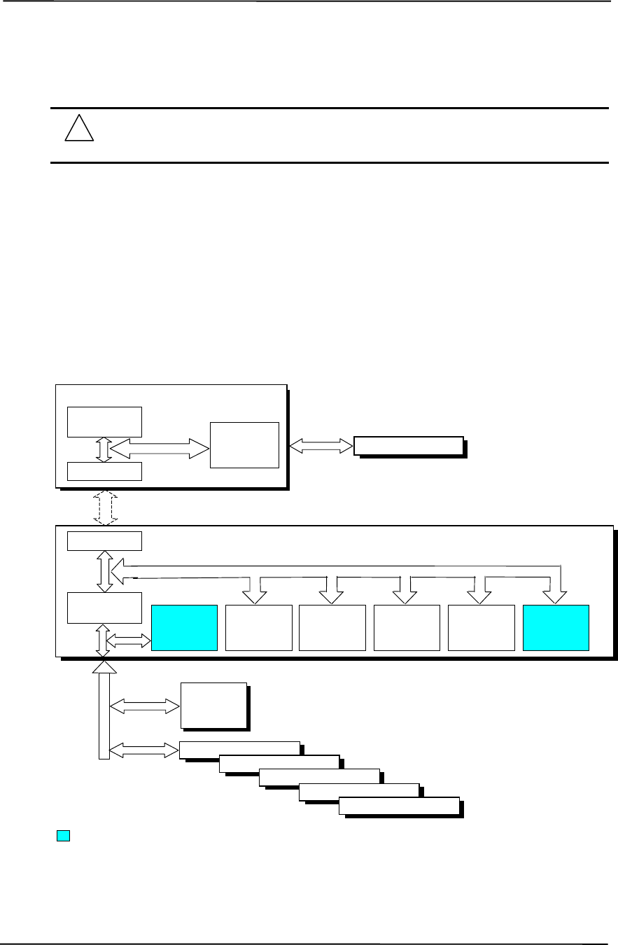
Chapter 4 System Support
Compaq Deskpro EXS and Workstation 300 Personal Computers
Featuring the Intel Pentium 4 Processor
First Edition - December 2000
4-2
4.2 PCI BUS OVERVIEW
NOTE: This section describes the PCI bus in general and highlights bus implementation
in this particular system. For detailed information regarding PCI bus operation, refer to
the PCI Local Bus Specification Revision 2.2.
This system implements a 32-bit Peripheral Component Interconnect (PCI) bus (spec. 2.2)
operating at 33 MHz. The PCI bus handles address/data transfers through the identification of
devices and functions on the bus. A device is typically defined as a component or slot that resides
on the PCI bus (although some components such as the MCH and ICH are organized as multiple
devices). A function is defined as the end source or target of the bus transaction. A device may
contain one or more functions.
In the standard configuration these systems use a hierarchy of three PCI buses (Figure 4-1). The
PCI bus #0 is internal to the MCH/ICH chipset components and is not physically accessible. The
AGP bus that services the AGP slot is designated as PCI bus #1. All PCI slots reside on PCI bus
#2.
Figure 4-1. PCI Bus Devices and Functions
Hub Link Bus
82850 MCH Component
AGP
Bridge
Function
Mem. Cntlr.
Function PCI
Bus #0
82801BA ICH2 Component
PCI Bridge
Function EIDE
Controller
Function
USB
I/F
Function
SMBus
Controller
Function
LPC
Bridge
Function
AC97
Audio
Function
PCI Bus #0
AGP Connector
PCI Bus #1
(AGP Bus)
Hub Link I/F
PCI
Bus #2
Hub Link I/F
NIC
I/F
Function
PCI Connector 1
PCI Connector 2
PCI Connector 3
PCI Connector 4
PCI Connector 5
Not used in these systems.
ES1373
Audio
Controller

Technical Reference Guide
Compaq Deskpro EXS and Workstation 300 Personal Computers
Featuring the Intel Pentium 4 Processor
First Edition - December 2000
4-3
4.2.1 PCI BUS TRANSACTIONS
The PCI bus consists of a 32-bit path (AD31-00 lines) that uses a multiplexed scheme for handling
both address and data transfers. A bus transaction consists of an address cycle and one or more
data cycles, with each cycle requiring a clock (PCICLK) cycle. High performance is realized
during burst modes in which a transaction with contiguous memory locations requires that only one
address cycle be conducted and subsequent data cycles are completed using auto-incremented
addressing. Four types of address cycles can take place on the PCI bus; I/O, memory,
configuration, and special. Address decoding is distributed (left up to each device on the PCI bus).
4.2.1.1 I/O and Memory Cycles
For I/O and memory cycles, a standard 32-bit address decode (AD31..0) for byte-level addressing
is handled by the appropriate PCI device. For memory addressing, PCI devices decode the
AD31..2 lines for dword-level addressing and check the AD1,0 lines for burst (linear-
incrementing) mode. In burst mode, subsequent data phases are conducted a dword at a time with
addressing assumed to increment accordingly (four bytes at a time).
4.2.1.2 Configuration Cycles
Devices on the PCI bus must comply with PCI protocol that allows configuration of that device by
software. In this system, configuration mechanism #1 (as described in the PCI Local Bus
specification Rev. 2.1) is employed. This method uses two 32-bit registers for initiating a
configuration cycle for accessing the configuration space of a PCI device. The configuration
address register (CONFIG_ADDRESS) at 0CF8h holds a value that specifies the PCI bus, PCI
device, and specific register to be accessed. The configuration data register (CONFIG_DATA) at
0CFCh contains the configuration data.
Bit Function Bit Function
31 Configuration Enable
0 = Disabled
1 = Enable
31..0 Configuration Data.
30..24 Reserved - read/write 0s
23..16 Bus Number. Selects PCI bus
15..11 PCI Device Number. Selects PCI
device for access
10..8 Function Number. Selects function of
selected PCI device.
7..2 Register Index. Specifies config. reg.
1,0 Configuration Cycle Type ID.
00 = Type 0
01 = Type 1
PCI Configuration Address Register
I/O Port 0CF8h, R/W, (32-bit access only) PCI Configuration Data Register
I/O Port 0CFCh, R/W, (8-, 16-, 32-bit access)

Chapter 4 System Support
Compaq Deskpro EXS and Workstation 300 Personal Computers
Featuring the Intel Pentium 4 Processor
First Edition - December 2000
4-4
Two types of configuration cycles are used. A Type 0 (zero) cycle is targeted to a device on the
PCI bus on which the cycle is running. A Type 1 cycle is targeted to a device on a downstream PCI
bus as identified by bus number bits <23..16>. With three or more PCI buses, a PCI bridge may
convert a Type 1 to a Type 0 if it’s destined for a device being serviced by that bridge or it may
forward the Type 1 cycle unmodified if it is destined for a device being serviced by a downstream
bridge. Figure 4-2 shows the configuration cycle format and how the loading of 0CF8h results in a
Type 0 configuration cycle on the PCI bus. The Device Number (bits <15..11> determines which
one of the AD31..11 lines is to be asserted high for the IDSEL signal, which acts as a “chip select”
function for the PCI device to be configured. The function number (CF8h, bits <10..8>) is used to
select a particular function within a PCI component.
Figure 4-2. Configuration Cycle
Table 4-1 shows the standard configuration access data for components and slots residing on a PCI
bus.
Table 4-1. PCI Device Configuration Access Data
Table 4-1.
PCI Component Configuration Access Data
PCI Component Vendor/Device ID PCI
Bus # Device # Function # IDSEL
Wired to:
82850 MCH:
Memory Controller
PCI/PCI (AGP) Bridge 8086h/2530h
8086h/2532h 0
00 (00h)
1 (01h) 0
0
--
AGP slot [3] 1 0 (00h) 0 --
82801BA ICH2:
PCI/PCI Bridge
LPC Bridge
EIDE Controller
USB I/F #1
SMBus Controller
USB I/F #2
AC97 Audio Controller [1]
AC97 Modem Controller [1]
Network Interface Controller [1]
8086h/244Eh
8086h/2440h
8086h/244Bh
8086h/2442h
8086h/2443h
8086h/2444h
8086h/2445h
8086h/2446h
8086h/2449h
0
0
0
0
0
0
0
0
2 [2]
30 (1Eh)
31 (1Fh)
31 (1Fh)
31 (1Fh)
31 (1Fh)
31 (1Fh)
31 (1Fh)
31 (1Fh)
8 (08h)
0
0
1
2
3
4
5
6
0
--
ES1373 Audio Controller 1274h/1373h 2 [2] 31 (1Fh) 0 AD22
PCI Connector 1 (PCI slot 1) [3] 2 [2] 4 (04h) 0 AD20
PCI Connector 2 (PCI slot 2) [3] 2 [2] 9 (09h) 0 AD25
PCI Connector 3 (PCI slot 3) [3] 2 [2] 10 (0Ah) 0 AD26
PCI Connector 3 (PCI slot 4) [3] 2 [2] 11 (0Bh) 0 AD27
PCI Connector 3 (PCI slot 5) [3] 2 [2] 13 (0Dh) 0 AD29
NOTES:
[1] Not implemented on these systems.
[2] Value in standard configuration. Can change if an AGP card with an additional bridge is installed.
[3] Card specific. Refer to appendices.
AD31..0
(w/Type 0
Config. Cycle)
Reserved Device
Number Function
Number Register
Index
Bus
Number
31 24 23 16 15 11 10 8 7 2 1 0 [1]
IDSEL (only one signal line asserted) Function
Number Register
Index
Register 0CF8h
Results in:
NOTES: [1] Bits <1,0> : 00 = Type 0 Cycle, 01 = Type 1 cycle
Type 1 cycle only. Reserved on Type 0 cycle.
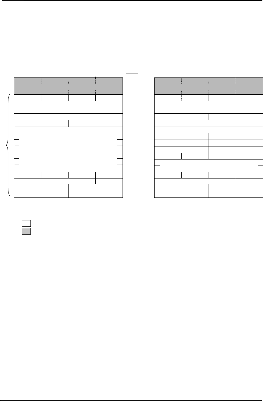
Technical Reference Guide
Compaq Deskpro EXS and Workstation 300 Personal Computers
Featuring the Intel Pentium 4 Processor
First Edition - December 2000
4-5
Not required
The register index (CF8h, bits <7..2>) identifies the 32-bit location within the configuration space
of the PCI device to be accessed. All PCI devices can contain up to 256 bytes of configuration data
(Figure 4-3), of which the first 64 bytes comprise the configuration space header.
Figure 4-3. PCI Configuration Space Mapping
Each PCI device is identified with a vendor ID (assigned to the vendor by the PCI Special Interest
Group) and a device ID (assigned by the vendor). The device and vendor IDs for the devices on
the system board are listed in Table 4-1.
Data required by PCI protocol
Configuration
Space
Header
PCI Configuration Space Type 1
Class Code
Command
31 24 23 16 15 8 7 0
Revision ID
Vendor ID
Status
Device ID
Ex
p
ansion ROM Base Address
Reserved
Prefetchable Limit U
pp
er 32 Bits
Prefetch. Mem. Limit Prefetch. Mem. Base
Prefetchable Base U
pp
er 32 Bits
Device-Specific Area
Line SizeLat. Timer
Int. LineInt. Pin
BIST Hdr. T
yp
e
Pri. Bus #Sec. Bus #Sub. Bus #2n
d
00h
Register
Index
04h
08h
0Ch
2Ch
30h
FCh
18h
28h
3Ch
38h
34h
40h
Brid
g
e Control
I/O Base U
pp
er 16 BitsI/O Limit U
pp
er 16 Bits
24h
20h
Memor
y
BaseMemor
y
Limit
I/O BaseI/O LimitSecondar
y
Status 1Ch
10h
Base Address Registers
00h
Register
Index
04h
08h
0Ch
2Ch
30h
FCh
10h
28h
3Ch
38h
34h
40h
Command
31 24 23 16 15 8 7 0
Revision ID
Vendor ID
Status
Device ID
Reserved
Reserved
Ex
p
ansion ROM Base Address
Subs
y
stem Vendor IDSubs
y
stem ID
Card Bus CIS Pointer
Device-Specific Area
Line SizeLat. Timer
Int. LineInt. PinMin. GNTMin. Lat.
BIST Hdr. T
yp
e
Class Code
Base Address Registers
PCI Configuration Space Type 0

Chapter 4 System Support
Compaq Deskpro EXS and Workstation 300 Personal Computers
Featuring the Intel Pentium 4 Processor
First Edition - December 2000
4-6
4.2.2 PCI BUS MASTER ARBITRATION
The PCI bus supports a bus master/target arbitration scheme. A bus master is a device that has
been granted control of the bus for the purpose of initiating a transaction. A target is a device that
is the recipient of a transaction. The Request (REQ), Grant (GNT), and FRAME signals are used
by PCI bus masters for gaining access to the PCI bus. When a PCI device needs access to the PCI
bus (and does not already own it), the PCI device asserts it’s REQn signal to the PCI bus arbiter (a
function of the system controller component). If the bus is available, the arbiter asserts the GNTn
signal to the requesting device, which then asserts FRAME and conducts the address phase of the
transaction with a target. If the PCI device already owns the bus, a request is not needed and the
device can simply assert FRAME and conduct the transaction. Table 4-2 shows the grant and
request signals assignments for the devices on the PCI bus.
Table 4-2. PCI Bus Mastering Devices
Table 4-2.
PCI Bus Mastering Devices
REQ/GNT Line Device
REQ0/GNT0 PCI Connector Slot 1
REQ1/GNT1 PCI Connector Slot 2
REQ2/GNT2 PCI Connector Slot 3
REQ3/GNT3 PCI Connector Slot 4
REQ4/GNT4 PCI Connector Slot 5
REQ5/GNT5 ES1373 Audio Controller
GREQ/GGNT AGP Slot
PCI bus arbitration is based on a round-robin scheme that complies with the fairness algorithm
specified by the PCI specification. The bus parking policy allows for the current PCI bus owner
(excepting the PCI/ISA bridge) to maintain ownership of the bus as long as no request is asserted
by another agent. Note that most CPU-to-DRAM and AGP-to-DRAM accesses can occur
concurrently with PCI traffic, therefore reducing the need for the Host/PCI bridge to compete for
PCI bus ownership.

Technical Reference Guide
Compaq Deskpro EXS and Workstation 300 Personal Computers
Featuring the Intel Pentium 4 Processor
First Edition - December 2000
4-7
4.2.3 OPTION ROM MAPPING
During POST, the PCI bus is scanned for devices that contain their own specific firmware in
ROM. Such option ROM data, if detected, is loaded into system memory’s DOS compatibility area
(refer to the system memory map shown in chapter 3).
4.2.4 PCI INTERRUPTS
Eight interrupt signals (INTA- thru INTH-) are available for use by PCI devices. These signals
may be generated by on-board PCI devices or by devices installed in the PCI slots. For more
information on interrupts including PCI interrupt mapping refer to the “System Resources” section
4.4.
4.2.5 PCI POWER MANAGEMENT SUPPORT
This system complies with the PCI Power Management Interface Specification (rev 1.0). The PCI
Power Management Enable (PME-) signal is supported by the chipset and allows compliant PCI
and AGP peripherals to initiate the power management routine.
4.2.6 PCI SUB-BUSSES
The chipset implements two data busses that are supplementary in operation to the PCI bus:
4.2.6.1 Hub Link Bus
The chipset implements a Hub Link bus between the MCH and the ICH. The Hub Link bus
handles transactions at a 66-MHz rate using PCI-type protocol, and in fact operates as PCI bus #0.
This bus is transparent to software and not accessible for expansion purposes.
4.2.6.2 LPC Bus
The 82801 ICH implements a Low Pin Count (LPC) bus for handling transactions to and from the
47B357 Super I/O Controller as well as the 82802 FWH. The LPC bus transfers data a nibble (4
bits) at a time at a 33-MHz rate. Generally transparent in operation, the LPC bus becomes a factor
primarily during the configuration of DMA channel modes (see section 4.4.3 “DMA”).

Chapter 4 System Support
Compaq Deskpro EXS and Workstation 300 Personal Computers
Featuring the Intel Pentium 4 Processor
First Edition - December 2000
4-8
4.2.7 PCI CONFIGURATION
PCI bus operations require the configuration of certain parameters such as PCI IRQ routing, DMA
channel configuration, RTC control, port decode ranges, and power management options. These
parameters are handled by the LPC I/F bridge function (PCI function #0, device 31) of the ICH
component and configured through the PCI configuration space registers listed in Table 4-3.
Configuration is provided by BIOS at power-up but re-configurable by software.
Table 4-3. LPC Bridge Configuration Registers (ICH, Function 0)
Table 4-3.
LPC Bridge Configuration Registers
(ICH, Function 0, Device 31)
PCI
Config.
Addr. Register Reset
Value
PCI
Config.
Addr. Register Reset
Value
00, 01h Vendor ID 8086h 8Ah Device 31 Error Status 00h
02, 03h Device ID 2410h 90, 91h PCI DMA Configuration 0000h
04, 05h Command 000Fh A0-CFh Power Management
06, 07h Status 0280h D0-D3h General Control 0’s
08h Revision ID 00h D4-D7h General Status F00h
0A-0Bh Class Code 0106h D8h RTC Configuration 00h
0Eh Header Type 80h E0h LPC COM Port Dec. Range 00h
40-43h ACPI Base Address 1 E1h LPC FDD & LPT Dec. Rge 00h
44h ACPI Control 00h E2h LPC Audio Dec. Range 80h
4E, 4Fh BIOS Control 0000h E3h FWH Decode Enable FFh
54h TCO Control 00h E4, E5h LPC I/F Decode Range 1 0000h
58-5Bh GPIO Base Address 1 E6, E7h LPC I/F Enables 0000h
5Ch GPIO Control 00h E8h FWH Select 00
60-63h INTA-D Routing Cntrl. 80h [1] EC, EDh LPC I/F Decode Range 2 0000h
64h Serial IRQ Control 10h EE, EFh Reserved --
65-87h Reserved -- F0h Reserved --
88h Dev. 31 Error Config. 00h F2h Function Disable Register 00h
NOTE: [1] Value for each byte.
Assume unmarked locations/gaps as reserved.

Technical Reference Guide
Compaq Deskpro EXS and Workstation 300 Personal Computers
Featuring the Intel Pentium 4 Processor
First Edition - December 2000
4-9
4.2.8 PCI CONNECTOR
Figure 4-4. PCI Bus Connector (32-Bit Type)
Table 4-4. PCI Bus Connector Pinout
Table 4-4.
PCI Bus Connector Pinout
Pin B Signal A Signal Pin B Signal A Signal Pin B Signal A Signal
01 -12 VDC TRST- 32 AD17 AD16 63 Reserved GND
02 TCK +12 VDC 33 C/BE2- +3.3 VDC 64 GND C/BE7-
03 GND TMS 34 GND FRAME- 65 C/BE6- C/BE5-
04 TDO TDI 35 IRDY- GND 66 C/BE4- +5 VDC
05 +5 VDC +5 VDC 36 +3.3 VDC TRDY- 67 GND PAR64
06 +5 VDC INTA- 37 DEVSEL- GND 68 AD63 AD62
07 INTB- INTC- 38 GND STOP- 69 AD61 GND
08 INTD- +5 VDC 39 LOCK- +3.3 VDC 70 +5 VDC AD60
09 PRSNT1- Reserved 40 PERR- SDONE n 71 AD59 AD58
10 RSVD +5 VDC 41 +3.3 VDC SBO- 72 AD57 GND
11 PRSNT2- Reserved 42 SERR- GND 73 GND AD56
12 GND GND 43 +3.3 VDC PAR 74 AD55 AD54
13 GND GND 44 C/BE1- AD15 75 AD53 +5 VDC
14 RSVD +3.3 AUX 45 AD14 +3.3 VDC 76 GND AD52
15 GND RST- 46 GND AD13 77 AD51 AD50
16 CLK +5 VDC 47 AD12 AD11 78 AD49 GND
17 GND GNT- 48 AD10 GND 79 +5 VDC AD48
18 REQ- GND 49 GND AD09 80 AD47 AD46
19 +5 VDC PME- 50 Key Key 81 AD45 GND
20 AD31 AD30 51 Key Key 82 GND AD44
21 AD29 +3.3 VDC 52 AD08 C/BE0- 83 AD43 AD42
22 GND AD28 53 AD07 +3.3 VDC 84 AD41 +5 VDC
23 AD27 AD26 54 +3.3 VDC AD06 85 GND AD40
24 AD25 GND 55 AD05 AD04 86 AD39 AD38
25 +3.3 VDC AD24 56 AD03 GND 87 AD37 GND
26 C/BE3- IDSEL 57 GND AD02 88 +5 VDC AD36
27 AD23 +3.3 VDC 58 AD01 AD00 89 AD35 AD34
28 GND AD22 59 +5 VDC +5 VDC 90 AD33 GND
29 AD21 AD20 60 ACK64- REQ64- 91 GND AD32
30 AD19 GND 61 +5 VDC +5 VDC 92 Reserved Reserved
31 +3.3 VDC AD18 62 +5 VDC +5 VDC 93 Reserved GND
-- -- -- -- -- -- 94 GND Reserved
B94
A94 A1
B1
B62
A62 A52
B52
A49
B49

Chapter 4 System Support
Compaq Deskpro EXS and Workstation 300 Personal Computers
Featuring the Intel Pentium 4 Processor
First Edition - December 2000
4-10
4.3 AGP BUS OVERVIEW
NOTE: This section provides a brief description of AGP bus operation. For a detailed
description of AGP bus operations as supported by these systems refer to the AGP
Interface Specification Rev. 2.0 available at the following AGP forum web site:
http://www.agpforum.org/index.htm
The Accelerated Graphics Port (AGP) bus is specifically designed as an economical yet high-
performance interface for graphics adapters, especially those designed for 3D operations. The
AGP interface is designed to give graphics adapters dedicated pipelined access to system memory
for the purpose of off-loading texturing, z-buffering, and alpha blending used in 3D graphics
operations. By off-loading a large portion of 3D data to system memory the AGP graphics adapter
only requires enough memory for frame buffer (display image) refreshing.
4.3.1 BUS TRANSACTIONS
The operation of the AGP bus is based on the 66-MHz PCI specification but includes additional
mechanisms to increase bandwidth. During the configuration phase the AGP bus acts in
accordance with PCI protocol. Once graphics data handling operation is initiated, AGP-defined
protocols take effect. The AGP graphics adapter acts generally as the AGP master, but can also
behave as a “PCI” target during fast writes from the MCH.
Key differences between the AGP interface and the PCI interface are as follows:
♦ Address phase and associated data transfer phase are disconnected transactions. Addressing
and data transferring occur as contiguous actions on the PCI bus. On the AGP bus a request
for data and the transfer of data may be separated by other operations.
♦ Commands on the AGP bus specify system memory accesses only. Unlike the PCI bus,
commands involving I/O and configuration are not required or allowed. The system memory
address space used in AGP operations is the same linear space used by PCI memory space
commands, but is further specified by the graphics address re-mapping table (GART) of the
north bridge component.
♦ Data transactions on the AGP bus involve eight bytes or multiples of eight bytes. The AGP
memory addressing protocol uses 8-byte boundaries as opposed to PCI’s 4-byte boundaries. If
a transfer of less than eight bytes is needed, the remaining bytes are filled with arbitrary data
that is discarded by the target.
♦ Pipelined requests are defined by length or size on the AGP bus. The PCI bus defines transfer
lengths with the FRAME- signal.
There are two basic types of transactions on the AGP bus: data requests (addressing) and data
transfers. These actions are separate from each other.

Technical Reference Guide
Compaq Deskpro EXS and Workstation 300 Personal Computers
Featuring the Intel Pentium 4 Processor
First Edition - December 2000
4-11
4.3.1.1 Data Request
Requesting data is accomplished in one of two ways; either multiplexed addressing (using the AD
lines for addressing/data) or demultiplexed (“sideband”) addressing (using the SBA lines for
addressing only and the AD lines for data only). Even though there are only eight SBA lines (as
opposed to the 32 AD lines) sideband addressing maximizes efficiency and throughput by allowing
the AD lines to be exclusively used for data transfers. Sideband addressing occurs at the same rate
(1X, 2X, or 4X) as data transfers. The differences in rates will be discussed in the next section
describing data transfers. Note also that sideband addressing is limited to 48 bits (address bits 48-
63 are assumed zero). The MCH component supports both SBA and AD addressing , but the
method and rate is selected by the AGP graphics adapter.
4.3.1.2 Data Transfers
Data transfers use the AD lines and occur as the result of data requests described previously. Each
transaction resulting from a request involves at least eight bytes, requiring the 32 AD lines to
handle at least two transfers per request. The 82850 MCH supports three transfer rates: 1X, 2X,
and 4X. Regardless of the rate used, the speed of the bus clock is constant at 66 MHz. The
following subsections describe how the use of additional strobe signals makes possible higher
transfer rates.
NOTE: These systems support only 1.5-volt signaling on the AGP bus.
AGP 1X Transfers
During a AGP 1X transfer the 66-MHz CLK signal is used to qualify the control and data signals.
Each 4-byte data transfer is synchronous with one CLK cycle so it takes two CLK cycles for a
minimum 8-byte transfer (Figure 4-5 shows two 8-byte transfers). The GNT- and TRDY- signals
retain their traditional PCI functions. The ST0..3 signals are used for priority encoding, with “000”
for low priority and “001” indicating high priority.
Figure 4-5. AGP 1X Data Transfer (Peak Transfer Rate: 266 MB/s)
T1 T2 T3 T4 T5 T6 T7
TRDY-
GNT-
CLK
AD D1A D2A D2BD1B
ST0..2 00x xxx xxx xxx xxx xxx
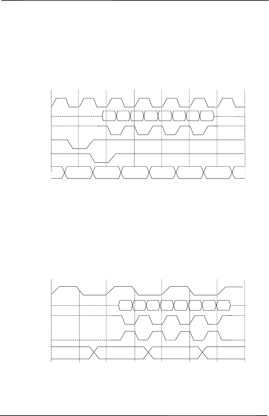
Chapter 4 System Support
Compaq Deskpro EXS and Workstation 300 Personal Computers
Featuring the Intel Pentium 4 Processor
First Edition - December 2000
4-12
AGP 2X Transfers
During AGP 2X transfers, clocking is basically the same as in 1X transfers except that the 66-MHz
CLK signal is used to qualify only the control signals. The data bytes are latched by an additional
strobe (AD_STBx) signal so that an 8-byte transfer occurs in one CLK cycle (Figure 4-6). The first
four bytes (DnA) are latched by the receiving agent on the falling edge of AD_STBx and the
second four bytes (DnB) are latched on the rising edge of AD_STBx.
Figure 4-6. AGP 2X Data Transfer (Peak Transfer Rate: 532 MB/s)
AGP 4X Transfers
The AGP 4X transfer rate allows sixteen bytes of data to be transferred in one clock cycle. As in
2X transfers the 66-MHz CLK signal is used only for qualifying control signals while strobe
signals are used to latch each 4-byte transfer on the AD lines. As shown in Figure 4-7, 4-byte block
DnA is latched by the falling edge of AD_STBx while DnB is latched by the falling edge of
AD_STBx-.
Figure 4-7. AGP 4X Data Transfer (Peak Transfer Rate: 1064 MB/s)
T1 T2 T3 T4 T5 T6 T7
TRDY-
GNT-
CLK
AD_STBx
AD D1A D2A D3A
D1B D2B D3B D4A D4B
ST0..2 00x xxx xxx xxx xxx xxx
T1 T2 T3 T4
AD_STBx
AD D1A D2A D3AD1B D2B D3B D4A D4B
CLK
AD_STBx-
00xxxx xxx xxx
ST0..2

Technical Reference Guide
Compaq Deskpro EXS and Workstation 300 Personal Computers
Featuring the Intel Pentium 4 Processor
First Edition - December 2000
4-13
4.3.2 AGP CONFIGURATION
AGP bus operations require the configuration of certain parameters involving system memory
access by the AGP graphics adapter. The AGP bus interface is configured as a PCI device
integrated within the north bridge (MCH, device 1) component. The AGP function is, from the PCI
bus perspective, treated essentially as a PCI/PCI bridge and configured through PCI configuration
registers (Table 4-6). Configuration is accomplished by BIOS during POST.
NOTE: Configuration of the AGP bus interface involves functions 0 and 1 of the MCH.
Function 0 registers (listed in Table 3-4) include functions that affect basic control
(GART) of the AGP.
Table 4-5. PCI/AGP Bridge Configuration Registers (MCH, Function 1)
Table 4-5.
PCI/AGP Bridge Function Configuration Registers
(MCH, Function 1)
PCI
Config.
Addr. Register Reset
Value
PCI
Config.
Addr. Register Reset
Value
00, 01h Vendor ID 8086h 1Bh Sec. Master Latency Timer 00h
02, 03h Device ID 2532h 1Ch I/O Base Address F0h
04, 05h Command 0000h 1Dh I/O Limit Address 00h
06, 07h Status 0020h 1E, 1Fh Sec. PCI/PCI Status 02A0h
08h Revision ID 00h 20, 21h Memory Base Address FFF0h
0A, 0Bh Class Code 0406h 22, 23h Memory Limit Address 0000h
0Eh Header Type 01h 24, 25h Prefetch Mem. Base Addr. FFF0h
18h Primary Bus Number 00h 26, 27h Prefetch Mem. Limit Addr. 0000h
19h Secondary Bus Number 00h 3Eh PCI/PCI Bridge Control 00h
1Ah Subordinate Bus Number 00h 3F-FFh Reserved 00h
NOTE: Assume unmarked locations/gaps as reserved. Refer to Intel documentation for detailed
register descriptions.
The AGP graphics adapter (actually its resident controller) is configured as a standard PCI device.

Chapter 4 System Support
Compaq Deskpro EXS and Workstation 300 Personal Computers
Featuring the Intel Pentium 4 Processor
First Edition - December 2000
4-14
4.3.3 AGP CONNECTOR
Figure 4-8. 1.5-Volt AGP Bus Connector
Table 4-6. AGP Bus Connector Pinout
Table 4-6.
AGP Bus Connector Pinout
Pin A Signal B Signal Pin A Signal B Signal Pin A Signal B Signal
01 +12 VDC OVRCNT- 23 GND GND 45 KEY KEY
02 Type Det- 5.0 VDC 24 Reserved VDD3 Aux 46 TRDY- DEVSEL-
03 Reserved 5.0 VDC 25 VDD3 VDD3 47 STOP- VDDQ
04 USB- USB+ 26 PAD30 PAD31 48 PME- PERR-
05 GND GND 27 PAD28 PAD29 49 GND GND
06 INTA- INTB- 28 VDD3 VDD3 50 PAR SERR-
07 RESET CLK 29 PAD26 PAD27 51 PAD15 CBE1-
08 GNT- REQ- 30 PAD24 PAD25 52 VDDQ VDDQ
09 VDD3 VDD3 31 GND GND 53 PAD13 PAD14
10 ST1 ST0 32 AD_STB1- AD_STB1 54 PAD11 PAD12
11 Reserved ST2 33 CBE3- PAD23 55 GND GND
12 PIPE- RBF- 34 VDDQ VDDQ 56 PAD09 PAD10
13 GND GND 35 PAD22 PAD21 57 CBE0- PAD08
14 WBF- Reserved 36 PAD20 PAD19 58 VDDQ VDDQ
15 SBA1 SBA0 37 GND GND 59 AD_STB0- AD_STB0
16 VDD3 VDD3 38 PAD18 PAD17 60 PAD06 PAD07
17 SBA3 SBA2 39 PAD16 CBE2- 61 GND GND
18 SB_STB- SB_STB 40 VDDQ VDDQ 62 PAD04 PAD05
19 GND GND 41 FRAME- IRDY- 63 PAD02 PAD03
20 SBA5 SBA4 42 KEY KEY 64 VDDQ VDDQ
21 SBA7 DBA6 43 KEY KEY 65 PAD00 PAD01
22 Reserved Reserved 44 KEY KEY 66 VREFGC VREFCG
NOTES: NC = Not connected
VDDQ = 1.5 VDC, as determined by system board grounding of Type Det- signal (pin A02).
B94
A94 B66
A66
A
1
B1
A41 A46
B41 B46
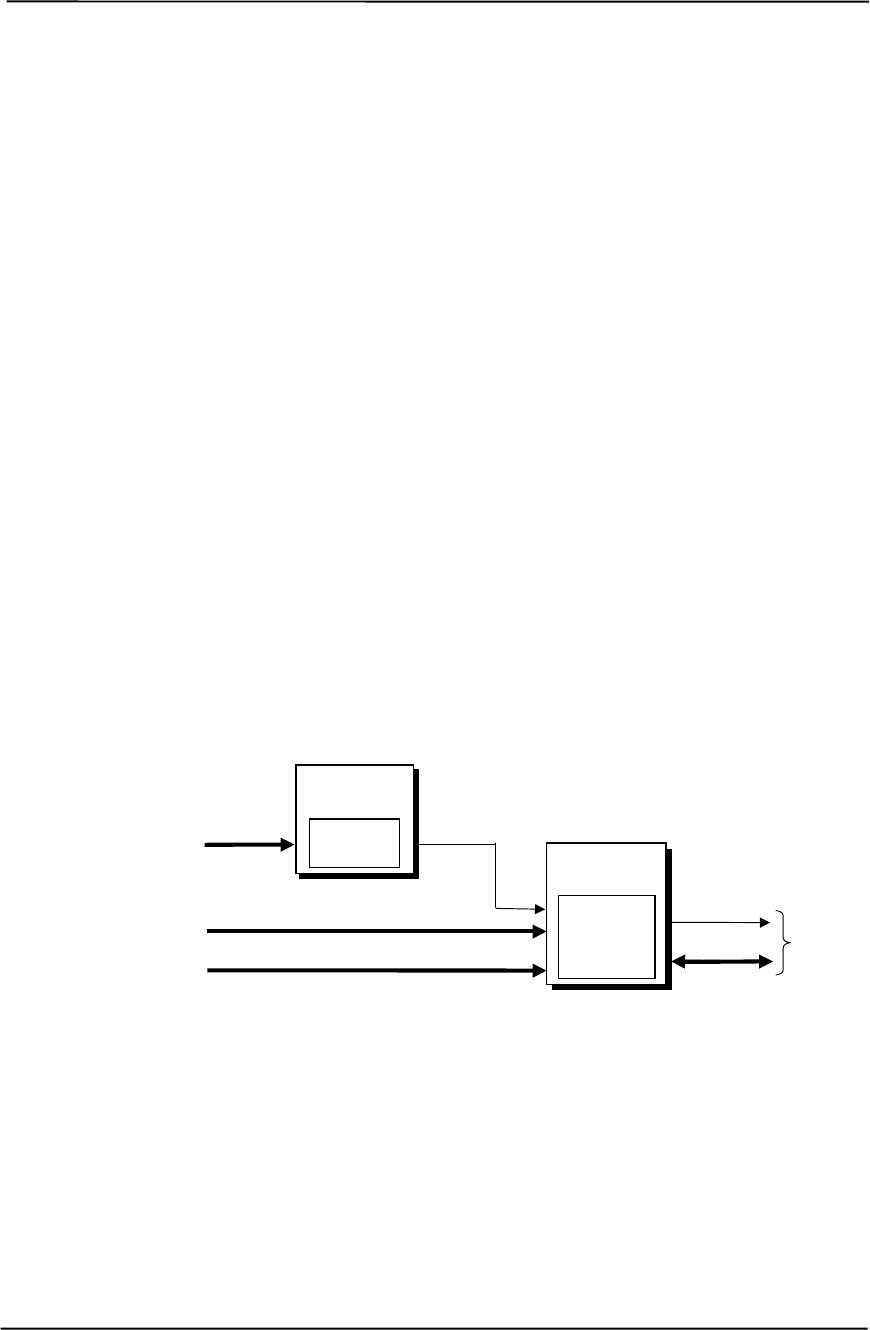
Technical Reference Guide
Compaq Deskpro EXS and Workstation 300 Personal Computers
Featuring the Intel Pentium 4 Processor
First Edition - December 2000
4-15
4.4 SYSTEM RESOURCES
This section describes the availability and basic control of major subsystems, otherwise known as
resource allocation or simply “system resources.” System resources are provided on a priority
basis through hardware interrupts and DMA requests and grants.
4.4.1 INTERRUPTS
The microprocessor uses two types of hardware interrupts; maskable and nonmaskable. A
maskable interrupt can be enabled or disabled within the microprocessor by the use of the STI and
CLI instructions. A nonmaskable interrupt cannot be masked off within the microprocessor,
although it may be inhibited by hardware or software means external to the microprocessor.
4.4.1.1 Maskable Interrupts
The maskable interrupt is a hardware-generated signal used by peripheral functions within the
system to get the attention of the microprocessor. Peripheral functions produce a unique INTA-H
(PCI) or IRQ0-15 (ISA) signal that is routed to interrupt processing logic that asserts the interrupt
(INTR-) input to the microprocessor. The microprocessor halts execution to determine the source
of the interrupt and then services the peripheral as appropriate. Figure 4-9 shows the routing of
PCI and ISA interrupts. Most IRQs are routed through the I/O controller, which contains a
serializing function. A serialized interrupt stream is applied to the 82801 ICH.
Figure 4-9. Maskable Interrupt Processing, Block Diagram
The 82801 ICH2 component can be configured (through the Setup utility) to handle interrupts in
one of two modes of operation:
♦ 8259 mode
♦ APIC mode
82801
ICH2
Interrupt
Processing
Serial IRQ
IRQ14,15
INTA-..D-
IRQ3..7,
9..12,
14,15
IDE
Hard Drives INTR-
Microprocessor
I/O &
SM Functions
PCI Peripherals
I/O Controller
Interrupt
Serializer
APIC Bus

Chapter 4 System Support
Compaq Deskpro EXS and Workstation 300 Personal Computers
Featuring the Intel Pentium 4 Processor
First Edition - December 2000
4-16
8259 Mode
In 8259-Mode, interrupts IRQ0-IRQ15 are handled in the conventional (AT-system) method using
logic that is the equivalent of two 8259 interrupt controllers. Table 4-7 lists the standard source
configuration for maskable interrupts and their priorities in 8259 mode. If more than one interrupt
is pending, the highest priority (lowest number) is processed first.
Table 4-7. Maskable Interrupt Priorities and Assignments
Table 4-7.
Maskable Interrupt Priorities and Assignments
Priority Signal Label Source (Typical)
1 IRQ0 Interval timer 1, counter 0
2 IRQ1 Keyboard
3 IRQ8- Real-time clock
4 IRQ9 Microtower, game/MIDI port; desktop or minitower, unused.
5 IRQ10 Unused
6 IRQ11 Unused
7 IRQ12 Mouse
8 IRQ13 Coprocessor (math)
9 IRQ14 IDE primary I/F
10 IRQ15 IDE secondary I/F
11 IRQ3 Serial port (COM2)
12 IRQ4 Serial port (COM1)
13 IRQ5 Unused
14 IRQ6 Diskette drive controller
15 IRQ7 Parallel port (LPT1)
-- IRQ2 NOT AVAILABLE (Cascade from interrupt controller 2)
APIC Mode
The Advanced Programmable Interrupt Controller (APIC) mode enhances interrupt-processing
performance with the following advantages:
♦ Eliminating the processor’s interrupt acknowledge cycle by using a separate APIC bus.
♦ Programmable interrupt priority.
♦ Additional interrupts (total of 24).
Eight PCI interrupts are available in APIC mode. The PCI interrupts are evenly distributed to
minimize latency and are hard-wired as follows:
ICH2
IRQ Cntlr. PCI
Slot 1 PCI
Slot 2 PCI
Slot 3 PCI
Slot 4 PCI
Slot 5 AGP
Slot USB
Cntlr. #1 USB
Cntlr. #2 Audio
Cntlr.
INTA- INTA- INTD- INTC- INTB- INTD- -- -- -- --
INTB- ------------ -- -- --
INTC- INTB- INTA- INTD- INTC- INTA- INTA- -- -- --
INTD- ----------INTB-INTD--- --
INTE- ------------ -- -- INTA-
INTF- INTC- INTB- INTA- INTD- INTB- -- -- -- --
INTG- INTD- INTC- INTB- INTA- INTC- -- -- -- --
INTH- ------------ --INTH---
Wired
to

Technical Reference Guide
Compaq Deskpro EXS and Workstation 300 Personal Computers
Featuring the Intel Pentium 4 Processor
First Edition - December 2000
4-17
NOTE: The APIC mode is supported by Windows NT/2000 operating systems. Systems
using the Windows 95 or 98 operating system will need to run in 8259 mode. The mode is
selectable through the Setup utility (access with F10 key during boot sequence).
Maskable Interrupt processing is controlled and monitored through standard AT-type I/O-mapped
registers. These registers are listed in Table 4-8.
Table 4-8. Maskable Interrupt Control Registers
Table 4-8.
Maskable Interrupt Control Registers
I/O Port Register
020h Base Address, Int. Cntlr. 1
021h Initialization Command Word 2-4, Int. Cntlr. 1
0A0h Base Address, Int. Cntlr. 2
0A1h Initialization Command Word 2-4, Int. Cntlr. 2
The initialization and operation of the interrupt control registers follows standard AT-type
protocol.
4.4.1.2 Non-Maskable Interrupts
Non-maskable interrupts cannot be masked (inhibited) within the microprocessor itself but may be
maskable by software using logic external to the microprocessor. There are two non-maskable
interrupt signals: the NMI- and the SMI-. These signals have service priority over all maskable
interrupts, with the SMI- having top priority over all interrupts including the NMI-.
NMI- Generation
The Non-Maskable Interrupt (NMI-) signal can be generated by one of the following actions:
♦ Parity errors detected on a PCI bus (activating SERR- or PERR-).
♦ Microprocessor internal error (activating IERRA or IERRB)
The SERR- and PERR- signals are routed through the ICH component, which in turn activates the
NMI to the microprocessor.

Chapter 4 System Support
Compaq Deskpro EXS and Workstation 300 Personal Computers
Featuring the Intel Pentium 4 Processor
First Edition - December 2000
4-18
The NMI Status Register at I/O port 061h contains NMI source and status data as follows:
NMI Status Register 61h
Bit Function
7 NMI Status:
0 = No NMI from system board parity error.
1 = NMI requested, read only
6IOCHK- NMI:
0 = No NMI from IOCHK-
1 = IOCHK- is active (low), NMI requested, read only
5 Interval Timer 1, Counter 2 (Speaker) Status
4 Refresh Indicator (toggles with every refresh)
3 IOCHK- NMI Enable/Disable:
0 = NMI from IOCHK- enabled
1 = NMI from IOCHK- disabled and cleared (R/W)
2 System Board Parity Error (PERR/SERR) NMI Enable:
0 = Parity error NMI enabled
1 = Parity error NMI disabled and cleared (R/W)
1 Speaker Data (R/W)
0 Inteval Timer 1, Counter 2 Gate Signal (R/W)
0 = Counter 2 disabled
1 = Counter 2 enabled
After the active NMI has been processed, status bits <7> or <6> are cleared by pulsing bits <2> or
<3> respectively.
The NMI Enable Register (070h, <7>) is used to enable/disable the NMI signal. Writing 80h to
this register masks generation of the NMI-. Note that the lower six bits of register at I/O port 70h
affect RTC operation and should be considered when changing NMI- generation status.
SMI- Generation
The SMI- (System Management Interrupt) is typically used for power management functions.
When power management is enabled, inactivity timers are monitored. When a timer times out,
SMI- is asserted and invokes the microprocessor’s SMI handler. The SMI- handler works with the
APM BIOS to service the SMI- according to the cause of the timeout.
Although the SMI- is primarily used for power managment the interrupt is also employed for the
QuickLock/QuickBlank functions as well.
Functions not related to NMI activity.

Technical Reference Guide
Compaq Deskpro EXS and Workstation 300 Personal Computers
Featuring the Intel Pentium 4 Processor
First Edition - December 2000
4-19
4.4.2 DIRECT MEMORY ACCESS
Direct Memory Access (DMA) is a method by which a device accesses system memory without
involving the microprocessor. Although the DMA method has been traditionally used to transfer
blocks of data to or from an ISA I/O device, PCI devices may also use DMA operation as well.
The DMA method reduces the amount of CPU interactions with memory, freeing the CPU for
other processing tasks.
NOTE: This section describes DMA in general. For detailed information regarding
DMA operation, refer to the data manual for the Intel 82801BA I/O Controller Hub.
The 82801 ICH2 component includes the equivalent of two 8237 DMA controllers cascaded
together to provide eight DMA channels, each (excepting channel 4) configurable to a specific
device. Table 4-9 lists the default configuration of the DMA channels.
Table 4-9. Default DMA Channel Assignments And Register I/O Ports
Table 4-9
DMA Channel Assignments And Register Ports
DMA Channel Function I/O Port
Controller 1 (byte transfers)
0
1
2
3
Unused
Audio subsystem
Diskette drive
Parallel port (ECP or EPP mode)
Control registers 000h-00Eh
Page register 087h
Page register 083h
Page register 081h
Page register 082h
Controller 2 (word transfers)
4
5
6
7
Cascade for controller 1
Unused
Unused
Unused
Control registers 0C0h-0DEh
n/a
Page register 08Bh
Page register 089h
Page register 08Ah
Refresh 08Fh [see note]
NOTE:
The DMA memory page register for the refresh channel must be
programmed with 00h for proper operation.
All channels in DMA controller 1 operate at a higher priority than those in controller 2. Note that
channel 4 is not available for use other than its cascading function for controller 1. The DMA
controller 2 can transfer words only on an even address boundary. The DMA controller and page
register define a 24-bit address that allows data transfers within the address space of the CPU.
In addition to device configuration, each channel can be configured (through PCI Configuration
Registers) for one of two modes of operation:
♦ LPC DMA Mode - Uses the LPC bus to communicate DMA channel control and is
implemented for devices using DMA through the I/O controller such as the diskette drive
controller.
♦ PC/PCI DMA Mode - Uses the REQ#/GNT# signals to communicate DMA channel control
and is used by PCI expansion devices.

Chapter 4 System Support
Compaq Deskpro EXS and Workstation 300 Personal Computers
Featuring the Intel Pentium 4 Processor
First Edition - December 2000
4-20
4.5 SYSTEM CLOCK DISTRIBUTION
These systems use an Intel CK-type clock generator and crystal for generating the clock signals
required by the system board components. Table 4-10 lists the system board clock signals and how
they are distributed.
Table 4-10. Clock Generation and Distribution
Table 4-10
Clock Generation and Distribution
Frequncy Source Destination
400 MHz MCH Processor, RIMM sockets
100 MHz CK MCH
66 MHz CK MCH, ICH2, AGP slot
48 MHz CK ICH2, I/O Cntlr.
33 MHz CK Processor, ICH2, PCI Slots
14.31818 MHz Crystal CK
Certain clock outputs are turned off during reduced power modes to conserve energy. Clock output
control is handled through the SMBus interface by BIOS.
4.6 REAL-TIME CLOCK AND CONFIGURATION MEMORY
The Real-time clock (RTC) and configuration memory (also referred to as “CMOS”) functions are
provided by the 82801 ICH component and is MC146818-compatible. As shown in the following
figure, the 82801 ICH component provides 256 bytes of battery-backed RAM divided into two
128-byte configuration memory areas. The RTC uses the first 14 bytes (00-0Dh) of the standard
memory area. All locations of the standard memory area (00-7Fh) can be directly accessed using
conventional OUT and IN assembly language instructions through I/O ports 70h/71h, although the
suggested method is to use the INT15 AX=E823h BIOS call.
Figure 4-10. Configuration Memory Map
A lithium 3-VDC battery is used for maintaining the RTC and configuration memory while the
system is powered down. The battery is located in a battery holder on the system board is replaced
with a Renata CR2032 or equivalent 3-VDC lithium battery.
RTC Area
(14 bytes)
Standard Config.
Memory Area
(114 bytes)
Extended Config.
Memory Area
(128 bytes)
00h
0Dh
0Eh
80h
FFh
7Fh
Seconds (Timer)
Minutes (Timer)
Seconds (Alarm)
Hours (Alarm)
Hours (Timer)
Minutes (Alarm)
Day of Week
Date of Month
Month
Year
Register A
Register B
Register C
Register D
00h
0Bh
01h
02h
03h
04h
05h
06h
07h
08h
09h
0Ah
0Dh
0Ch
82801
C
M
OS

Technical Reference Guide
Compaq Deskpro EXS and Workstation 300 Personal Computers
Featuring the Intel Pentium 4 Processor
First Edition - December 2000
4-21
4.6.1 CLEARING CMOS
The contents of configuration memory (including the Power-On Password) can be cleared by the
following procedures:
1. Turn off the unit.
2. Disconnect the AC power cord from the outlet and/or system unit.
3. Remove the chassis hood (cover) and insure that no LEDs on the system board are
illuminated.
4. Press and release the CMOS clear button on the system board.
5. Replace the chassis hood (cover).
6. Reconnect the AC power cord to the outlet and/or system unit.
7. Turn the unit on.
To clear only the Power-On Password refer to section 4.7.1.1.

Chapter 4 System Support
Compaq Deskpro EXS and Workstation 300 Personal Computers
Featuring the Intel Pentium 4 Processor
First Edition - December 2000
4-22
4.6.2 CMOS ARCHIVE AND RESTORE
During the boot sequence the BIOS saves a copy of NVRAM (CMOS contents, password(s) and
other system variables) in a portion of the flash ROM. Should the system become un-usable, the
last good copy of NVRAM data can be restored with the Power Button Override function. This
function is invoked with the following procedure:
1. With the unit powered down, press and release the power button.
2. Immediately after releasing the power button in step 1, press and hold the power button until
the unit powers down. This action will be recorded as a Power Button Override event.
With the next startup sequence the BIOS will detect the occurrence of the Power Button Override
event and will load the backup copy of NVRAM from the ROM to the CMOS.
NOTE: The Power Button Override feature does not allow quick cycling of the system
(turning on then off). If the power cord is disconnected during the POST routine, the
splash screen image may become corrupted, requiring a re-flashing of the ROM (refer to
chapter 8, BIOS ROM).
4.6.3 STANDARD CMOS LOCATIONS
Table 4-14 and the following paragraphs describe standard configuration memory locations 0Ah-
3Fh. These locations are accessible using OUT/IN assembly language instructions using port
70/71h or BIOS function INT15, AX=E823h.
Table 4-11. Configuration Memory (CMOS) Map
Table 4-11.
Configuration Memory (CMOS) Map
Location Function Location Function
00-0Dh Real-time clock 24h System board ID
0Eh Diagnostic status 25h System architecture data
0Fh System reset code 26h Auxiliary peripheral configuration
10h Diskette drive type 27h Speed control external drive
11h Reserved 28h Expanded/base mem. size, IRQ12
12h Hard drive type 29h Miscellaneous configuration
13h Security functions 2Ah Hard drive timeout
14h Equipment installed 2Bh System inactivity timeout
15h Base memory size, low byte/KB 2Ch Monitor timeout, Num Lock Cntrl
16h Base memory size, high byte/KB 2Dh Additional flags
17h Extended memory, low byte/KB 2Eh-2Fh Checksum of locations 10h-2Dh
18h Extended memory, high byte/KB 30h-31h Total extended memory tested
19h Hard drive 1, primary controller 32h Century
1Ah Hard drive 2, primary controller 33h Miscellaneous flags set by BIOS
1Bh Hard drive 1, secondary controller 34h International language
1Ch Hard drive 2, secondary controller 35h APM status flags
1Dh Enhanced hard drive support 36h ECC POST test single bit
1Eh Reserved 37h-3Fh Power-on password
1Fh Power management functions 40-FFh Feature Control/Status
NOTES: Assume unmarked gaps are reserved.

Technical Reference Guide
Compaq Deskpro EXS and Workstation 300 Personal Computers
Featuring the Intel Pentium 4 Processor
First Edition - December 2000
4-23
RTC Control Register A, Byte 0Ah
Bit Function
7 Update in Progress. Read only.
0 = Time update will not occur before 2444 us
1 = Time update will occur within 2444 us
6..4 Divider Chain Control. R/W.
00x = Oscillator disabled.
010 = Normal operation (time base frequency = 32.768 KHz).
11x = Divider chain reset.
3..0 Periodic Interrupt Control. R/W. Specifies the periodic interrupt interval.
0000 = none 1000 = 3.90625 ms
0001 = 3.90625 ms 1001 = 7.8125 ms
0010 = 7.8125 ms 1010 = 15. 625 ms
0011 = 122.070 us 1011 = 31.25 ms
0100 = 244.141 us 1100 = 62.50 ms
0101 = 488.281 us 1101 = 125 ms
0110 = 976.562 us 1110 = 250 ms
0111 = 1.953125 ms 1111 = 500 ms
RTC Control Register B, Byte 0Bh
Bit Function
7 Time Update Enable/disable
0 = Normal operation, 1 = Disable time updating for time set
6 Periodic Interrupt Enable/Disable.
0 = Disable, 1 = Enable interval specified by Register A
5 Alarm Interrupt Enable/disable
0 = Disabled, 1 = Enabled
4 End-of-Update Interrupt Enable/Disable
0 = Disabled, 1 = Enabled
3 Reserved (read 0)
2 Time/Date Format Select
0 = BCD format, 1 = Binary format
1 Time Mode
0 = 12-hour mode, 1 = 24-hour mode
0 Automatic Daylight Savings Time Enable/Disable
0 = Disable
1 = Enable (Advance 1 hour on 1st Sunday in April, retreat 1 hour on last Sunday in
October).
RTC Status Register C, Byte 0Ch
Bit Function
7 If set, interrupt output signal active (read only)
6 If set, indicates periodic interrupt flag
5 If set, indicates alarm interrupt
4 If set, indicates end-of-update interrupt
3..0 Reserved
RTC Status Register D, Byte 0Dh
Bit Function
7 RTC Power Status
0 = RTC has lost power
1 = RTC has not lost power
6..0 Reserved

Chapter 4 System Support
Compaq Deskpro EXS and Workstation 300 Personal Computers
Featuring the Intel Pentium 4 Processor
First Edition - December 2000
4-24
Configuration Byte 0Eh, Diagnostic Status
Default Value = 00h
This byte contains diagnostic status data.
Configuration Byte 0Fh, System Reset Code
Default Value = 00h
This byte contains the system reset code.
Configuration Byte 10h, Diskette Drive Type
Bit Function
7..4 Primary (Drive A) Diskette Drive Type
3..0 Secondary (Drive B) Diskette Drive Type
Valid values for bits <7..4> and bits <3..0>:
0000 = Not installed
0001 = 360-KB drive
0010 = 1.2-MB drive
0011 = 720-KB drive
0100 = 1.44-MB/1.25-MB drive
0110 = 2.88-MB drive
(all other values reserved)
Configuration Byte 12h, Hard Drive Type
Bit Function
7..4 Primary Controller 1, Hard Drive 1 Type:
0000 = none 1000 = Type 8
0001 = Type 1 1001 = Type 9
0010 = Type 2 1010 = Type 10
0011 = Type 3 1011 = Type 11
0100 = Type 4 1100 = Type 12
0101 = Type 5 1101 = Type 13
0110 = Type 6 1110 = Type 14
0111 = Type 7 1111 = other (use bytes 19h)
3..0 Primary Controller 1, Hard Drive 2 Type:
0000 = none 1000 = Type 8
0001 = Type 1 1001 = Type 9
0010 = Type 2 1010 = Type 10
0011 = Type 3 1011 = Type 11
0100 = Type 4 1100 = Type 12
0101 = Type 5 1101 = Type 13
0110 = Type 6 1110 = Type 14
0111 = Type 7 1111 = other (use bytes 1Ah)

Technical Reference Guide
Compaq Deskpro EXS and Workstation 300 Personal Computers
Featuring the Intel Pentium 4 Processor
First Edition - December 2000
4-25
Configuration Byte 13h, Security Functions
Default Value = 00h
Bit Function
7 Reserved
6 QuickBlank Enable After Standby:
0 = Disable
1 = Enable
5 Administrator Password:
0 = Not present
1 = Present
4 Reserved
3 Diskette Boot Enable:
0 = Enable
1 = Disable
2 QuickLock Enable:
0 = Disable
1 = Enable
1 Network Server Mode/Security Lock Override:
0 = Disable
1 = Enable
0 Password State (Set by BIOS at Power-up)
0 = Not set
1 = Set
Configuration Byte 14h, Equipment Installed
Default Value (standard configuration) = 03h
Bit Function
7,6 No. of Diskette Drives Installed:
00 = 1 drive 10 = 3 drives
01 = 2 drives 11 = 4 drives
5..2 Reserved
1 Coprocessor Present
0 = Coprocessor not installed
1 = Coprocessor installed
0 Diskette Drives Present
0 = No diskette drives installed
1 = Diskette drive(s) installed
Configuration Bytes 15h and 16h, Base Memory Size
Default Value = 280h
Bytes 15h and 16h hold a 16-bit value that specifies the base memory size in 1-KB (1024)
increments. Valid base memory sizes are 512 and 640 kilobytes .
Configuration Bytes 17h and 18h, Extended Memory Size
Bytes 17h and 18h hold a 16-bit value that specifies the extended memory size in 1-KB
increments.

Chapter 4 System Support
Compaq Deskpro EXS and Workstation 300 Personal Computers
Featuring the Intel Pentium 4 Processor
First Edition - December 2000
4-26
Configuration Bytes 19h-1Ch, Hard Drive Types
Byte 19h contains the hard drive type for drive 1 of the primary controller if byte 12h bits <7..4>
hold 1111b. Byte 1Ah contains the hard drive type for drive 2 of the primary controller if byte 12h
bits <3..0> hold 1111b. Bytes1Bh and 1Ch contain the hard drive types for hard drives 1 and 2 of
the secondary controller.
Configuration Byte 1Dh, Enhanced IDE Hard Drive Support
Default Value = F0h
Bit Function
7 EIDE - Drive C (83h)
6 EIDE - Drive D (82h)
5 EIDE - Drive E (81h)
4 EIDE - Drive F (80h)
3..0 Reserved
Values for bits <7..4> :
0 = Disable
1 = Enable for auto-configure
Configuration Byte 1Fh, Power Management Functions
Default Value = 00h
Bit Function
7..4 Reserved
3 Slow Processor Clock for Low Power Mode
0 = Processor runs at full speed
1 = Processor runs at slow speed
2 Reserved
1 Monitor Off Mode
0 = Turn monitor power off after 45 minutes in
standby
1 = Leave monitor power on
0 Energy Saver Mode Indicator (Blinking LED)
0 = Disable
1 = Enable
Configuration Byte 24h, System Board Identification
Default Value = 7Eh
Configuration memory location 24h holds the system board ID.
Configuration Byte 25h, System Architecture Data
Default Value = 0Bh
Bit Function
7..4 Reserved
3 Unmapping of ROM:
0 = Allowed
1 = Not allowed
2 Reserved
1,0 Diagnostic Status Byte Address
00 = Memory locations 80C00000h-80C00004h
01 = I/O ports 878h-87Ch
11 = neither place

Technical Reference Guide
Compaq Deskpro EXS and Workstation 300 Personal Computers
Featuring the Intel Pentium 4 Processor
First Edition - December 2000
4-27
Configuration Byte 26h, Auxiliary Peripheral Configuration
Default Value = 00h
Bit Function
7,6 I/O Delay Select
00 = 420 ns (default)
01 = 300 ns
10 = 2600 ns
11 = 540 ns
5 Alternative A20 Switching
0 = Disable port 92 mode
1 = Enable port 92 mode
4 Bi-directional Print Port Mode
0 = Disabled
1 = Enabled
3 Graphics Type
0 = Color
1 = Monochrome
2 Hard Drive Primary/Secondary Address Select:
0 = Primary
1 = Secondary
1 Diskette I/O Port
0 = Primary
1 = Secondary
0 Diskette I/O Port Enable
0 = Primary
1 = Secondary
Configuration Byte 27h, Speed Control/External Drive
Default Value = 00h
Bit Function
7 Boot Speed
0 = Max MHz
1 = Fast speed
6..0 Reserved
Configuration Byte 28h, Expanded and Base Memory, IRQ12 Select
Default Value = 00h
Bit Function
7 IRQ12 Select
0 = Mouse
1 = Expansion bus
6,5 Base Memory Size:
00 = 640 KB
01 = 512 KB
10 = 256 KB
11 = Invalid
4..0 Internal Compaq Memory:
00000 = None
00001 = 512 KB
00010 = 1 MB
00011 = 1.5 MB
.
.
11111 = 15.5 MB

Chapter 4 System Support
Compaq Deskpro EXS and Workstation 300 Personal Computers
Featuring the Intel Pentium 4 Processor
First Edition - December 2000
4-28
Configuration Byte 29h, Miscellaneous Configuration Data
Default Value = 00h
Bit Function
7..5 Reserved
4 Primary Hard Drive Enable (Non-PCI IDE Controllers)
0 = Disable
1 = Enable
3..0 Reserved
Configuration Byte 2Ah, Hard Drive Timeout
Default Value = 02h
Bit Function
7..5 Reserved
4..0 Hard Drive Timeout (index to SIT timeout record)
Configuration Byte 2Bh, System Inactivity Timeout
Default Value = 23h
Bit Function
7 Reserved
6,5 Power Conservation Boot
00 = Reserved
01 = PC on
10 = PC off
11 = Reserved
4..0 System Inactive Timeout. (Index to SIT system timeout
record)
00000 = Disabled
Configuration Byte 2Ch, ScreenSave and NUMLOCK Control
Default Value = 00h
Bit Function
7 Reserved
6 Numlock Control
0 = Numlock off at power on
1 = Numlock on at power on
5 Screen Blank Control:
0 = No screen blank
1 = Screen blank w/QuickLock
4..0 ScreenSave Timeout. (Index to SIT monitor timeout record)
000000 = Disabled

Technical Reference Guide
Compaq Deskpro EXS and Workstation 300 Personal Computers
Featuring the Intel Pentium 4 Processor
First Edition - December 2000
4-29
Configuration Byte 2Dh, Additional Flags
Default Value = 00h
Bit Function
7..5 Reserved
4 Memory Test
0 = Test memory on power up only
1 = Test memory on warm boot
3 POST Error Handling (BIOS Defined)
0 = Display “Press F1 to Continue” on error
1 = Skip F1 message
2..0 Reserved
Configuration Byte 2Eh, 2Fh, Checksum
These bytes hold the checksum of bytes 10h to 2Dh.
Configuration Byte 30h, 31h, Total Extended Memory Tested
This location holds the amount of system memory that checked good during the POST.
Configuration Byte 32h, Century
This location holds the Century value in a binary coded decimal (BCD) format.
Configuration Byte 33h, Miscellaneous Flags
Default Value = 80h
Bit Function
7 Memory Above 640 KB
0 = No, 1 = Yes
6 Reserved
5 Weitek Numeric Coprocessor Present:
0 = Not installed, 1 = Installed
4 Standard Numeric Coprocessor Present:
0 = Not installed, 1 = Installed
3..0 Reserved
Configuration Byte 34h, International Language Support
Default Value = 00h

Chapter 4 System Support
Compaq Deskpro EXS and Workstation 300 Personal Computers
Featuring the Intel Pentium 4 Processor
First Edition - December 2000
4-30
Configuration Byte 35h, APM Status Flags
Default Value = 11h
Bit Function
7..6 Power Conservation State:
00 = Ready
01 = Standby
10 = Suspend
11 = Off
5,4 Reserved
3 32-bit Connection:
0 = Disconnected, 1 = Connected
2 16-bit Connection
0 = Disconnected, 1 = Connected
1 Real Mode Connection
0 = Disconnected, 1 = Connected
0 Power Management Enable:
0 = Disabled
1 = Enabled
Configuration Byte 36h, ECC POST Test Single Bit Errors
Default Value = 01h
Bit Function
7 Row 7 Error Detect
6 Row 6 Error Detect
5 Row 5 Error Detect
4 Row 4 Error Detect
3 Row 3 Error Detect
2 Row 2 Error Detect
1 Row 1 Error Detect
0 Row 0 Error Detect
0 = No single bit error detected.
1 = Single bit error detected.
Configuration Byte 37h-3Fh, Power-On Password
These eight locations hold the power-on password.

Technical Reference Guide
Compaq Deskpro EXS and Workstation 300 Personal Computers
Featuring the Intel Pentium 4 Processor
First Edition - December 2000
4-31
4.7 SYSTEM MANAGEMENT
This section describes functions having to do with security, power management, temperature, and
overall status. These functions are handled by hardware and firmware (BIOS) and generally
configured through the Setup utility.
4.7.1 SECURITY FUNCTIONS
These systems include various features that provide different levels of security. Note that this
subsection describes only the hardware functionality (including that supported by Setup) and
does not describe security features that may be provided by the operating system and application
software.
4.7.1.1 Power-On Password
These systems include a power-on password, which may be enabled or disabled (cleared) through
a jumper on the system board. The jumper controls a GPIO input to the 82801 ICH that is checked
during POST. The password is stored in configuration memory (CMOS) and if enabled and then
forgotten by the user will require that either the password be cleared (preferable solution and
described below) or the entire CMOS be cleared (refer to section 4.6).
To clear the password, use the following procedure:
1. Turn off the system and disconnect the AC power cord from the outlet and/or system unit.
2. Remove the cover (hood). Insure that all system board LEDs are off (not illuminated).
3. Locate the password header/jumper (labeled E49 on these systems) and remove the jumper
from pins 1 and 2 and place on (just) pin 2 (for safekeeping).
4. Replace the cover.
5. Re-connect the AC power cord to the AC outlet and/or system unit.
6. Turn on the system. The POST routine will clear and disable the password.
7. To re-enable the password feature, repeat steps 1-6, replacing the jumper on pins 1 and 2 of
header E49.
4.7.1.2 Setup Password
The Setup utility may be configured to be always changeable or changeable only by entering a
password. The password is held on CMOS and, if forgotten, will require that CMOS be cleared
(refer to section 4.6).

Chapter 4 System Support
Compaq Deskpro EXS and Workstation 300 Personal Computers
Featuring the Intel Pentium 4 Processor
First Edition - December 2000
4-32
4.7.1.3 Cable Lock Provision
These systems include a chassis cutout (on the rear panel) for the attachment of a cable lock
mechanism.
4.7.1.4 I/O Interface Security
The serial, parallel, USB, and diskette interfaces may be disabled individually through the Setup
utility to guard against unauthorized access to a system. In addition, the ability to write to or boot
from a removable media drive (such as the diskette drive) may be enabled through the Setup
utility. The disabling of the serial, parallel, and diskette interfaces are a function of the
LPC47B357 I/O controller. The USB ports are controlled through the 82801 ICH.
4.7.2 POWER MANAGEMENT
These systems provide baseline hardware support of ACPI- and APM-compliant firmware and
software. Key power-consuming components (processor, chipset, I/O controller, and fan) can be
placed into a reduced power mode either automatically or by user control. The system can then be
brought back up (“wake-up”) by events defined by the ACPI specification. The ACPI wake-up
events supported by this system are listed as follows:
ACPI Wake-Up Event System Wakes From
Power Button Suspend or soft-off
RTC Alarm Suspend or soft-off
Wake On LAN (w/NIC) Suspend or soft-off
PME Suspend or soft-off
Serial Port Ring Suspend or soft-off
USB Suspend only
Keyboard Suspend only
Mouse Suspend only

Technical Reference Guide
Compaq Deskpro EXS and Workstation 300 Personal Computers
Featuring the Intel Pentium 4 Processor
First Edition - December 2000
4-33
4.7.3 SYSTEM STATUS
These systems provide a visual indication of system boot and ROM flash status through the
keyboard LEDs as listed in table 4-12.
NOTE: The LED indications listed in Table 4-12 are valid only for PS/2-type
keyboards. A USB keyboard will not provide LED status for the listed events, although
audible (beep) indications will occur.
Table 4-12. System Boot/ROM Flash Status LED Indications
Table 4-12.
System Boot/ROM Flash Status LED Indications
Event NUM Lock
LED CAPs Lock
LED Scroll Lock
LED
System memory failure [1] Blinking Off Off
Graphics controller failure [2] Off Blinking Off
System failure prior to graphics cntlr. initialization [3] Off Off Blinking
ROMPAQ diskette not present, faulty, or drive prob. On Off Off
Password prompt Off On Off
Invalid ROM detected - flash failed Blinking [4] Blinking [4] Blinking [4]
Keyboard locked in network mode Blinking [5] Blinking [5] Blinking [5]
Successful boot block ROM flash On [6] On [6] On [6]
NOTES: [1] Accompanied by 1 short, 2 long audio beeps
[2] Accompanied by 1 long, 2 short audio beeps
[3] Accompanied by 2 long, 1 short audio beeps
[4] All LEDs will blink in sync twice, accompanied by 1 long and three short audio beeps
[5] LEDs will blink in sequence (NUM Lock, then CAPs Lock, then Scroll Lock)
[6] Accompanied by rising audio tone.
Table 4-13 lists the operation status codes provided by the power LED on the front of the chassis.
Note that error or problem conditions are reported only by the power LED on the minitower.
Table 4-13. System Operational Status LED Indications
Table 4-13.
System Operational Status LED Indications
System Status Desktop
Power LED Minitower
Power LED
S0: System on (normal operation) Steady green Steady green
S1: Suspend Blinks green @ 1 Hz Blinks green @ 1 Hz
S3: Suspend to RAM Blinks green @ 1 Hz Blinks green @ 1 Hz
S4: Suspend to disk Blinks green @ 0.5 Hz Blinks green @ 0.5 Hz
S5: Soft off Off - clear Off - clear
Processor not seated Off - clear Steady red
CPU thermal shutdown Off - clear Blinks red @ 4 Hz
ROM error Off - clear Blinks red @ 1 Hz
Power supply crowbar activated Off - clear Blinks red @ .5 Hz
System off Off - clear Off
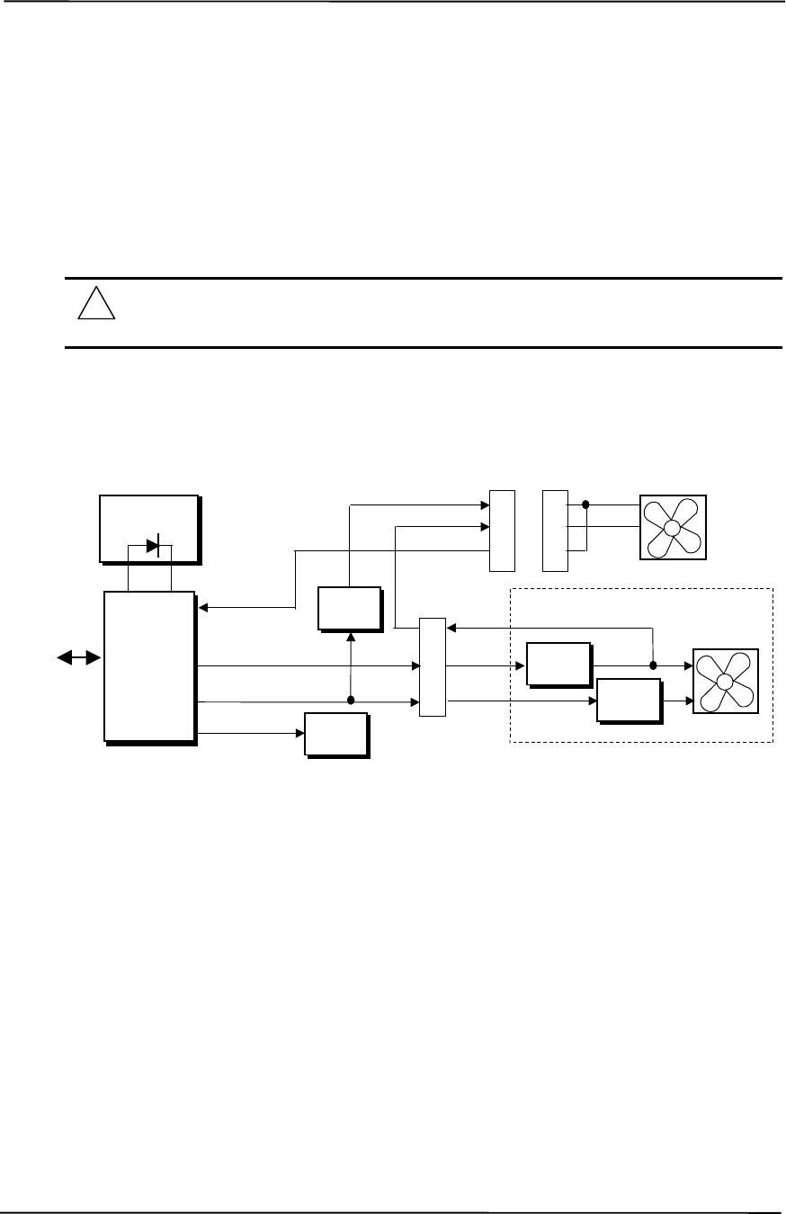
Chapter 4 System Support
Compaq Deskpro EXS and Workstation 300 Personal Computers
Featuring the Intel Pentium 4 Processor
First Edition - December 2000
4-34
4.7.4 TEMPERATURE SENSING AND COOLING
These systems feature a fan integrated into the power supply assembly. A separate chassis fan is
also employed. Both fans are variable-speed type, and typically operate in tandem as long as the
power supply is active (producing 12 VDC). The fans are off in S3 (Suspend-to-RAM) and S5
(Soft-Off) states.
NOTE: These systems are designed to provide optimum cooling with the cover in place.
Operating a system with the cover removed may result in a thermal condition of system
board components, including the processor.
Figure 4-11 shows the fan control schematic.
NOTE: [1] Will be +12 VDC if chassis fan is connected and operating.
Figure 4-11. Fan Control Block Diagram
An ASIC monitors a thermal diode internal to the processor and provides a Fan CMD signal that
the Speed Control logic of the power supply uses to vary the speed of the fans through the negative
power rail. The turning off of the fans as the result from the system being placed into a Sleep
condition is initiated by the ASIC asserting the Fan Off- signal, which results in the On/Off Control
logic shutting off the +12 volts to the fans.
Typical cooling conditions include the following:
1. Normal – Low fan speed.
2. Hot processor – ASIC directs Speed Control logic to increase speed of fan(s).
3. Hot power supply – Power supply increases speed of fan(s).
4. Sleep state – Fans turned off. Hot processor or power supply will result in starting fans.
Power Supply Assembly
P1
Speed
Control
Fan CMD
Fan Off- Fan
Off
PS Fan
CMD
Processor
Sensing
ASIC
On/Off
Control (+)
(-)
CH Fan CMD
Fan
Sense [1]
SMBus
ICH2
82801
ICH2
Therm-
On/Off
Control
8
12
24 PS Fan
(+)
(-)
2
3
4
Chassis Fan
Header P8
2
3
4(+)
(-)

Technical Reference Guide
Compaq Deskpro EXS and Workstation 300 Personal Computers
Featuring the Intel Pentium 4 Processor
First Edition - December 2000
4-35
4.8 REGISTER MAP AND MISCELLANEOUS FUNCTIONS
This section contains the system I/O map and information on general-purpose functions of the ICH
and I/O controller.
4.8.1 SYSTEM I/O MAP
Table 4-14 lists the fixed addresses of the input/output (I/O) ports.
Table 4-14. System I/O Map
Table 4-14.
System I/O Map
I/O Port Function
0000..001Fh DMA Controller 1
0020..002Dh Interrupt Controller 1
002E, 002Fh Index, Data Ports to LPC47B357 I/O Controller (primary)
0030..003Dh Interrupt Controller
0040..0042h Timer 1
004E, 004Fh Index, Data Ports to LPC47B357 I/O Controller (secondary)
0050..0052h Timer / Counter
0060..0067h Microcontroller, NMI Controller (alternating addresses)
0070..0077h RTC Controller
0080..0091h DMA Controller
0092h Port A, Fast A20/Reset Generator
0093..009Fh DMA Controller
00A0..00B1h Interrupt Controller 2
00B2h, 00B3h APM Control/Status Ports
00B4..00BDh Interrupt Controller
00C0..00DFh DMA Controller 2
00F0h Coprocessor error register
0170..0177h IDE Controller 2 (active only if standard I/O space is enabled for primary drive)
01F0..01F7h IDE Controller 1 (active only if standard I/O space is enabled for secondary drive)
0278..027Fh Parallel Port (LPT2)
02E8..02EFh Serial Port (COM4)
02F8..02FFh Serial Port (COM2)
0370..0377h Diskette Drive Controller Secondary Address
0376h IDE Controller 2 (active only if standard I/O space is enabled for primary drive)
0378..037Fh Parallel Port (LPT1)
03B0..03DFh Graphics Controller
03BC..03BEh Parallel Port (LPT3)
03E8..03EFh Serial Port (COM3)
03F0..03F5h Diskette Drive Controller Primary Addresses
03F6h IDE Controller 1 (active only if standard I/O space is enabled for sec. drive)
03F8..03FFh Serial Port (COM1)
04D0, 04D1h Interrupt Controller
0678..067Fh Parallel Port (LPT2)
0778..077Fh Parallel Port (LPT1)
07BC..07BEh Parallel Port (LPT3)
0CF8h PCI Configuration Address (dword access only )
0CF9h Reset Control Register
0CFCh PCI Configuration Data (byte, word, or dword access)
NOTE: Assume unmarked gaps are unused, reserved, or used by functions that employ variable I/O
address mapping. Some ranges may include reserved addresses.

Chapter 4 System Support
Compaq Deskpro EXS and Workstation 300 Personal Computers
Featuring the Intel Pentium 4 Processor
First Edition - December 2000
4-36
4.8.2 82801 ICH GENERAL PURPOSE FUNCTIONS
The 82801 ICH2 component includes a number of single and multi-purpose pins available as
general-purpose input/output (GPIO) ports. The GPIO ports are configured (enabled/disabled)
during POST by BIOS through the PCI configuration registers of the ICH’s LPC I/F Bridge
(82801, function 0). The GPIO ports are controlled through 64 bytes of I/O space that is mapped
during POST.
Table 4-15 lists the utilization of the ICH’s GPIO ports in the desktop and minitower systems.
Table 4-15. 82801 ICH GPIO Register Utilization (Desktop and Minitower only)
Table 4-15.
82801 ICH2 GPIO Register Utilization
GPIO Port # Function Direction
0PS LED I
1NIC REQ5 I
2IRQE- I
3IRQF- I
4 IRQG- I
5 IRQH- I
6HD LED I
7-- NC
8NC
12 TAFI ASIC Interrupt I
13 SMI I
18 -- NC
19 -- NC
20 -- NC
21 -- NC
22 -- NC
23 -- NC
24 NC
25 -- NC
26 NC
27 NC
28 Password Enable I
NOTE: NC = not connected (not used).

Technical Reference Guide
Compaq Deskpro EXS and Workstation 300 Personal Computers
Featuring the Intel Pentium 4 Processor
First Edition - December 2000
4-37
4.8.3 I/O CONTROLLER FUNCTIONS
The I/O controller (used in desktop and minitower systems) contains various functions such as the
keyboard/mouse interfaces, diskette interface, serial interfaces, and parallel interface. While the
control of these interfaces uses standard AT-type I/O addressing (as described in chapter 5) the
configuration of these functions occurs through indexed ports using PnP protocol. In these
systems, hardware strapping selects I/O addresses 02Eh/02Fh at reset as the Index/Data ports for
accessing the logical devices within the I/O contoller. Table 4-16 lists the PnP control registers for
the LPC47B357.
Table 4-16 LPC47B357 Control Registers
Table 4-16.
I/O Controller Control Registers
Index Function Reset Value
02h Configuration Control 00h
03h Reserved
07h Logical Device (Interface) Select:
00h = Diskette Drive I/F
01h = Rsvd
02h = Rsvd
03h = Parallel I/F
04h = Serial I/F (UART 1)
05h = Serial I/F (UART 2)
06h = Rsvd
07h = Keyboard I/F
08h = Rsvd
09h = Rsvd
0Ah = Runtime Reg. (GPIO Config.)
0Bh = Rsvd
00h
20h Super I/O ID Register (SID) 56H
21h Revision --
22h Logical Device Power Control 00h
23h Logical Device Power Management 00h
24h PLL / Oscillator Control 04h
25-2Fh Device specific [2] --
NOTES: Refer to LPC47B357 data sheet for detailed register information.
The configuration registers are accessed through I/O registers 2Eh (index) and 2Fh (data) after the
configuration phase has been activated by writing 55h once to I/O port 2Eh. The BIOS then
initiates each logical device and then deactivates the configuration phase by writing AAh to 2Eh.

Chapter 4 System Support
Compaq Deskpro EXS and Workstation 300 Personal Computers
Featuring the Intel Pentium 4 Processor
First Edition - December 2000
4-38
4.8.3.1 LPC47B357 GPIO Utilization
The LPC47B357 I/O Controller (used in desktop and minitower systems) provides 62 general-
purpose pins that can be individually configured for specific purposes. These pins are configured
through the Runtime registers (logical device 0Ah) during the system’s configuration phase of the
boot sequence by the BIOS.
Table 4-17 lists the GPIO registers for the LPC47B357. Note that not all ports are listed as this
table defines only the custom implementation of GPIO ports. Refer to SMC documentation for
standard usage of unlisted GPIO ports.
Table 4-17. LPC47B357 GPIO Register Utilization (Desktop and Minitower only)
Table 4-17.
LPC47B357 GPIO Port Utilization
GPIO Function Direction GPIO Function Direction
10 Board rev 1 I 42 ICH SCI O
11 Board rev 0 I 43 -- NC
12 -- NC 44 Hood Lock NC
13 PME- I 45 Hood Unlock NC
14 WOL NC 46 ICH SMI- O
15 System ID 4 [1] I 60 PCI Slot Reset O
16 Processor Fan sense I 61 AGP Slot Reset O
17 -- NC 62 PWR Button In I
20 Pri. IDE 80-pin Cable Detect I 63 SLP S3 I
21 Sec. IDE 80-pin Cable Detect I 64 SLP S5 I
22 -- NC 65 CPU Changed/Removed O
23 System ID 2 [1] I 66 PWR Button Out O
24 BIOS fail for AOL O 67 PS On O
25 System ID 3 [1] I 70 Remote Off I
26 Processor Present I 71 System ID 0 [1] NC
27 -- NC 72 System ID 1 [1] NC
30 PS LED Color Grn O 73 -- NC
31 PS LED Blink O 74 -- NC
32 Thermal Trip I 75 -- NC
33 2 MB Media ID I 76 -- NC
34 FWH Write Protect O 85 Pwr SEL O
35 FWH Reset O 86 S3 3.3 VDC On O
36 Diskette Motor B O -- -- --
37 Diskette Select B O -- -- --
NOTE: NC = Not connected (not used).
[1] System ID (ID4..0) value for these systems = 00111.

Technical Reference Guide
Compaq Deskpro EXS and Workstation 300 Personal Computers
Featuring the Intel Pentium 4 Processor
First Edition - December 2000
4-39
4.8.3.2 LPC47B357 I/O Controller Miscellaneous Functions
The desktop and minitower systems utilize the following specialized functions built into the LPC
47B357 I/O Controller:
♦ Power/Hard drive LED control – The I/O controller provides color and blink control for the
front panel LEDs used for indicating system events as listed below:
System Status Power LED HD LED
S0: System on (normal operation) Steady green Green w/HD activity
S1: Suspend Blinks green @ 1 Hz Off
S3: Suspend to RAM Blinks green @ 1 Hz Off
S4: Suspend to disk Blinks green @ 0.5 Hz Off
S5: Soft off Off - clear Off
Backplane board not seated Steady red Steady red
Processor not seated Steady red Off
CPU thermal shutdown Blinks red @ 4 Hz Off
ROM error Blinks red @ 1 Hz Off
Power supply crowbar activated Blinks red @ 0.5 Hz Off
System off Off Off
♦ I/O security – The parallel, serial, and diskette interfaces may be disabled individually by
software and the LPC47B357’s disabling register locked. If the disabling register is locked, a
system reset through a cold boot is required to gain access to the disabling (Device Disable)
register.
♦ Processor present/speed detection – One of the battery-back general-purpose inputs (GPI26)
of the LPC47B357 detects if the processor has been removed. The occurrence of this event is
passed to the ICH that will, during the next boot sequence, initiate the speed selection routine
for the processor. The speed selection function replaces the manual DIP switch configuration
procedure required on previous systems.
♦ Legacy/ACPI power button mode control – The LPC47B357 receives the pulse signal from
the system’s power button and produces the PS On signal according to the mode (legacy or
ACPI) selected. Refer to chapter 7 for more information regarding power management.

Chapter 4 System Support
Compaq Deskpro EXS and Workstation 300 Personal Computers
Featuring the Intel Pentium 4 Processor
First Edition - December 2000
4-40
This page is intentionally blank.

Technical Reference Guide
Compaq Deskpro EXS and Workstation 300 Personal Computers
Featuring the Intel Pentium 4 Processor
First Edition - December 2000
5-1
Chapter 5
INPUT/OUTPUT INTERFACES
5. Chapter 5 INPUT/OUTPUT INTERFACES
5.1 INTRODUCTION
This chapter describes the standard (i.e., system board) interfaces that provide input and output
(I/O) porting of data and specifically discusses interfaces that are controlled through I/O-mapped
registers. The following I/O interfaces are covered in this chapter:
♦ Enhanced IDE interface (5.2) page 5-1
♦ Diskette drive interface (5.3) page 5-4
♦ Serial interfaces (5.4) page 5-8
♦ Parallel interface (5.5) page 5-11
♦ Keyboard/pointing device interface (5.6) page 5-16
♦ Universal serial bus interface (5.7) page 5-22
♦ Audio subsystem (5.8) page 5-26
♦ Network support (5.9) page 5-33
5.2 ENHANCED IDE INTERFACE
The enhanced IDE (EIDE) interface consists of primary and secondary controllers integrated into
the 82801 ICH2 component of the chipset. Two 40-pin IDE connectors (one for each controller)
are included on the system board. Each controller can be configured independently for the
following modes of operation:
♦ Programmed I/O (PIO) mode – CPU controls drive transactions through standard I/O mapped
registers of the IDE drive.
♦ 8237 DMA mode – CPU offloads drive transactions using DMA protocol with transfer rates
up to 16 MB/s.
♦ Ultra ATA/100 mode – Preferred bus mastering source-synchronous protocol providing
transfer rates of 100 MB/s.
NOTE: These systems include 80-conductor data cables required for UATA/66 and /100
modes.
5.2.1 IDE PROGRAMMING
The IDE interface is configured as a PCI device during POST and controlled through I/O-mapped
registers at runtime.

Chapter 5 Input/Output Interfaces
5-2 Compaq Deskpro EXS and Workstation 300 Personal Computers
Featuring the Intel Pentium 4 Processor
First Edition – December 2000
Hard drives types not found in the ROM’s parameter table are automatically configured as to
(soft)type by DOS as follows:
Primary controller: drive 0, type 65; drive 1, type 66
Secondary controller: drive 0, type 68; drive 1, type 15
Non-DOS (non-Windows) operating systems may require using Setup (F10) for drive
configuration.
5.2.1.1 IDE Configuration Registers
The IDE controller is configured as a PCI device with bus mastering capability. The PCI
configuration registers for the IDE controller function (PCI device #31, function #1) are listed in
Table 5-1.
Table 5–1. IDE PCI Configuration Registers
Table 5-1.
EIDE PCI Configuration Registers (82801, Device 31/Function 1)
PCI Conf.
Addr. Register Reset
Value PCI Conf.
Addr. Register Reset
Value
00-01h Vender ID 8086h 0F..1Fh Reserved 0’s
02-03h Device ID 244Bh 20-23h BMIDE Base Address 1
04-05h PCI Command 0000h 2C, 2Dh Subsystem Vender ID 0000h
06-07h PCI Status 0280h 2E, 2Fh Subsystem ID 0000h
08h Revision ID 00h 30..3Fh Reserved 0’s
09h Programming 80h 40-43h Pri./Sec. IDE Timing 0’s
0Ah Sub-Class 01h 44h Slave IDE Timing 00h
0Bh Base Class Code 01h 48h Sync. DMA Control 00h
0Dh Master Latency Timer 00h 4A-4Bh Sync. DMA Timing 0000h
0Eh Header Type 00h 54h EIDE I/O Config.Register 00h
NOTE: Assume unmarked gaps are reserved and/or not used.
5.2.1.2 IDE Bus Master Control Registers
The IDE interface can perform PCI bus master operations using the registers listed in Table 5-2.
These registers occupy 16 bytes of variable I/O space set by software and indicated by PCI
configuration register 20h in the previous table.
Table 5–2. IDE Bus Master Control Registers
Table 5-2.
IDE Bus Master Control Registers
I/O Addr.
Offset Size
(Bytes) Register Default
Value
00h 1 Bus Master IDE Command (Primary) 00h
02h 1 Bus Master IDE Status (Primary) 00h
04h 4 Bus Master IDE Descriptor Pointer (Pri.) 0000 0000h
08h 1 Bus Master IDE Command (Secondary) 00h
0Ah 2 Bus Master IDE Status (Secondary) 00h
0Ch 4 Bus Master IDE Descriptor Pointer (Sec.) 0000 0000h
NOTE: Unspecified gaps are reserved, will return indeterminate data, and should not be written to.
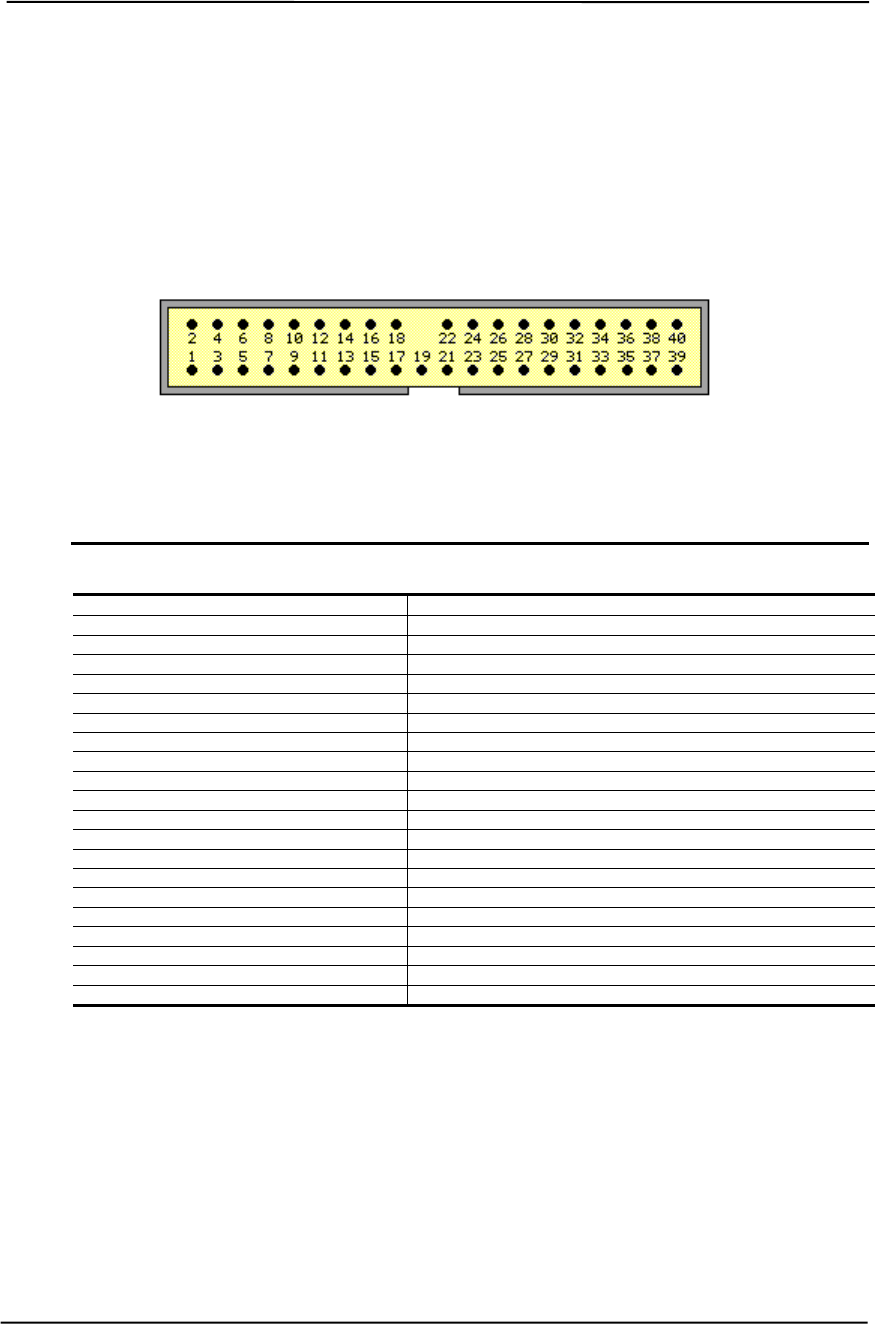
Technical Reference Guide
Compaq Deskpro EXS and Workstation 300 Personal Computers
Featuring the Intel Pentium 4 Processor
First Edition - December 2000
5-3
5.2.2 IDE CONNECTOR
This system uses a standard 40-pin connector for the primary IDE device and connects (via a
cable) to the hard drive installed in the right side drive bay. Note that some signals are re-defined
for UATA/33 and UATA/66 modes, which require a special 80-conductor cable (supplied)
designed to reduce cross-talk. Device power is supplied through a separate connector.
Figure 5-1. 40-Pin Primary IDE Connector (on system board).
Table 5–3. 40-Pin Primary IDE Connector Pinout
Table 5-3.
40-Pin Primary IDE Connector Pinout
Pin Signal Description Pin Signal Description
1 RESET- Reset 21 DRQ DMA Request
2 GND Ground 22 GND Ground
3 DD7 Data Bit <7> 23 IOW- I/O Write [1]
4 DD8 Data Bit <8> 24 GND Ground
5 DD6 Data Bit <6> 25 IOR- I/O Read [2]
6 DD9 Data Bit <9> 26 GND Ground
7 DD5 Data Bit <5> 27 IORDY I/O Channel Ready [3]
8 DD10 Data Bit <10> 28 CSEL Cable Select
9 DD4 Data Bit <4> 29 DAK- DMA Acknowledge
10 DD11 Data Bit <11> 30 GND Ground
11 DD3 Data Bit <3> 31 IRQn Interrupt Request [4]
12 DD12 Data Bit <12> 32 IO16- 16-bit I/O
13 DD2 Data Bit <2> 33 DA1 Address 1
14 DD13 Data Bit <13> 34 DSKPDIAG Pass Diagnostics
15 DD1 Data Bit <1> 35 DA0 Address 0
16 DD14 Data Bit <14> 36 DA2 Address 2
17 DD0 Data Bit <0> 37 CS0- Chip Select
18 DD15 Data Bit <15> 38 CS1- Chip Select
19 GND Ground 39 HDACTIVE- Drive Active (front panel LED) [5]
20 -- Key 40 GND Ground
NOTES: [1] On UATA/33 and higher modes, re-defined as STOP.
[2] On UATA/33 and higher mode reads, re-defined as DMARDY-.
On UATA/33 and higher mode writes, re-defined as STROBE.
[3] On UATA/33 and higher mode reads, re-defined as STROBE-.
On UATA/33 and higher mode writes, re-defined as DMARDY-.
[4] Primary connector wired to IRQ14, secondary connector wired to IRQ15.
[5] Pin 39 is used for spindle sync and drive activity (becomes SPSYNC/DACT-)
when synchronous drives are connected.

Chapter 5 Input/Output Interfaces
5-4 Compaq Deskpro EXS and Workstation 300 Personal Computers
Featuring the Intel Pentium 4 Processor
First Edition – December 2000
5.3 DISKETTE DRIVE INTERFACE
The diskette drive interface supports up to two diskette drives, each of which use a common cable
connected to a standard 34-pin diskette drive connector. All models come standard with a 3.5-inch
1.44-MB diskette drive installed as drive A. The drive designation is determined by which
connector is used on the diskette drive cable. The drive attached to the end connector is drive A
while the drive attached to the second (next to the end) connector) is drive B.
On all models, the diskette drive interface function is integrated into the LPC47B357 super I/O
component. The internal logic of the I/O controller is software-compatible with standard 82077-
type logic. The diskette drive controller has three operational phases in the following order:
♦ Command phase - The controller receives the command from the system.
♦ Execution phase - The controller carries out the command.
♦ Results phase - Status and results data is read back from the controller to the system.
The Command phase consists of several bytes written in series from the CPU to the data register
(3F5h/375h). The first byte identifies the command and the remaining bytes define the parameters
of the command. The Main Status register (3F4h/374h) provides data flow control for the diskette
drive controller and must be polled between each byte transfer during the Command phase.
The Execution phase starts as soon as the last byte of the Command phase is received. An
Execution phase may involve the transfer of data to and from the diskette drive, a mechnical
control function of the drive, or an operation that remains internal to the diskette drive controller.
Data transfers (writes or reads) with the diskette drive controller are by DMA, using the DRQ2 and
DACK2- signals for control.
The Results phase consists of the CPU reading a series of status bytes (from the data register
(3F5h/375h)) that indicate the results of the command. Note that some commands do not have a
Result phase, in which case the Execution phase can be followed by a Command phase.
During periods of inactivity, the diskette drive controller is in a non-operation mode known as the
Idle phase.

Technical Reference Guide
Compaq Deskpro EXS and Workstation 300 Personal Computers
Featuring the Intel Pentium 4 Processor
First Edition - December 2000
5-5
5.3.1 DISKETTE DRIVE PROGRAMMING
Programming the diskette drive interface consists of configuration, which occurs typically during
POST, and control, which occurs at runtime.
5.3.1.1 Diskette Drive Interface Configuration
The diskette drive controller must be configured for a specific address and also must be enabled
before it can be used. Address selection and enabling of the diskette drive interface are affected by
firmware through the PnP configuration registers of the 47B357 I/O controller during POST.
The configuration registers are accessed through I/O registers 2Eh (index) and 2Fh (data) after the
configuration phase has been activated by writing 55h to I/O port 2Eh. The diskette drive I/F is
initiated by firmware selecting logical device 0 of the 47B357 using the following sequence:
1. Write 07h to I/O register 2Eh.
2. Write 00h to I/O register 2Fh (this selects the diskette drive I/F).
3. Write 30h to I/O register 2Eh.
4. Write 01h to I/O register 2Fh (this activates the interface).
Writing AAh to 2Eh deactivates the configuration phase. The diskette drive I/F configuration
registers are listed in the following table:
Table 5–4. Diskette Drive Controller Configuration Registers
Table 5-4.
Diskette Drive Interface Configuration Registers
Index
Address Function R/W Reset
Value
30h Activate R/W 01h
60-61h Base Address R/W 03F0h
70h Interrupt Select R/W 06h
74h DMA Channel Select R/W 02h
F0h DD Mode R/W 02h
F1h DD Option R/W 00h
F2h DD Type R/W FFh
F4h DD 0 R/W 00h
F5h DD 1 R/W 00h
For detailed configuration register information refer to the SMSC data sheet for the LPC47B357
I/O component.
5.3.1.2 Diskette Drive Interface Control
The BIOS function INT 13 provides basic control of the diskette drive interface. The diskette drive
interface can be controlled by software through the LPC47B357’s I/O-mapped registers listed in
Table 5-5. The diskette drive controller of the LPC47B357 operates in the PC/AT mode in these
systems.
Table 5–5. Diskette Drive Interface Control Registers

Chapter 5 Input/Output Interfaces
5-6 Compaq Deskpro EXS and Workstation 300 Personal Computers
Featuring the Intel Pentium 4 Processor
First Edition – December 2000
Table 5-5.
Diskette Drive Interface Control Registers
Pri.
Addr. Sec.
Addr. Register R/W
3F0h 370h Status Register A:
<7> Interrupt pending
<6> Reserved (always 1)
<5> STEP pin status (active high)
<4> TRK 0 status (active high)
<3> HDSEL status (0 = side 0, 1 = side 1)
<2> INDEX status (active high)
<1> WR PRTK status (0 = disk is write protected)
<0> Direction (0 = outward, 1 = inward)
R
3F1h 371h Status Register B:
<7,6> Reserved (always 1’s)
<5> DOR bit 0 status
<4> Write data toggle
<3> Read data toggle
<2> WGATE status (active high)
<1,0> MTR 2, 1 ON- status (active high)
R
3F2h 372h Digital Output Register (DOR):
<7,6> Reserved
<5,4> Motor 1, 0 enable (active high)
<3> DMA enable (active high)
<2> Reset (active low)
<1,0> Drive select (00 = Drive 1, 01 = Drive 2, 10 = Reserved, 11 = Tape drive)
R/W
3F3h 373h Tape Drive Register (available for compatibility) R/W
3F4h 374h Main Status Register (MSR):
<7> Request for master (host can transfer data) (active high)
<6> Transfer direction (0 – write, 1 = read)
<5> non-DMA execution (active high)
<4> Command busy (active high)
<3,2> Reserved
<1,0> Drive 1, 2 busy (active high)
Data Rate Select Register (DRSR):
<7> Software reset (active high)
<6> Low power mode enable (active high)
<5> Reserved (0)
<4..2> Precompensation select (default = 000)
<1,0> Data rate select (00 = 500 Kb/s, 01 = 300 Kb/s, 10 = 250 Kb/s, 11 = 2/1
Mb/s)
R
W
3F5h 375h Data Register:
<7..0> Data R/W
3F6h 376h Reserved --
3F7h 377h Digital Input Register (DIR):
<7> DSK CHG status (records opposite value of pin)
<6..0> Reserved (0’s)
Configuration Control Register (CCR):
<7..2> Reserved
<1,0> Data rate select (00 = 500 Kb/s, 01 = 300 Kb/s, 10 = 250 Kb/s, 11 = 2/1
Mb/s)
R
W
NOTE: The most recently written data rate value to either DRSR or CCR will be in effect.

Technical Reference Guide
Compaq Deskpro EXS and Workstation 300 Personal Computers
Featuring the Intel Pentium 4 Processor
First Edition - December 2000
5-7
5.3.2 DISKETTE DRIVE CONNECTOR
This system uses a standard 34-pin connector (refer to Figure 5-2 and Table 5-6 for the pinout) for
diskette drives. Drive power is supplied through a separate connector.
Figure 5-2. 34-Pin Diskette Drive Connector.
Table 5–6. 34-Pin Diskette Drive Connector Pinout
Table 5-6.
34-Pin Diskette Drive Connector Pinout
Pin Signal Description Pin Signal Description
1 GND Ground 18 DIR- Drive head direction control
2 LOW DEN- Low density select 19 GND Ground
3 --- (KEY) 20 STEP- Drive head track step control
4 MEDIA ID- Media identification 21 GND Ground
5 GND Ground 22 WR DATA- Write data
6DRV 4
SEL- Drive 4 select 23 GND Ground
7 GND Ground 24 WR ENABLE- Enable for WR DATA-
8 INDEX- Media index is detected 25 GND Ground
9 GND Ground 26 TRK 00- Heads at track 00 indicator
10 MTR 1 ON- Activates drive motor 27 GND Ground
11 GND Ground 28 WR PRTK- Media write protect status
12 DRV 2
SEL- Drive 2 select 29 GND Ground
13 GND Ground 30 RD DATA- Data and clock read off disk
14 DRV 1
SEL- Drive 1 select 31 GND Ground
15 GND Ground 32 SIDE SEL- Head select (side 0 or 1)
16 MTR 2 ON- Activates drive motor 33 GND Ground
17 GND Ground 34 DSK CHG- Drive door opened indicator
1
2 4
5
6
7
8
9
10
11
12
13
14
15
16
17
18
19
20
21
22
23
24
25
26
27
28
29
30
31
32
33
34
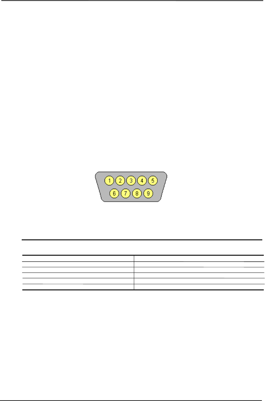
Chapter 5 Input/Output Interfaces
5-8 Compaq Deskpro EXS and Workstation 300 Personal Computers
Featuring the Intel Pentium 4 Processor
First Edition – December 2000
5.4 SERIAL INTERFACE
All models include two serial interfaces to transmit and receive asynchronous serial data with
external devices. The serial interface function is provided by the LPC47B357 I/O controller
component that includes two NS16C550-compatible UARTs.
Each UART supports the standard baud rates up through 115200, and also special high speed rates
of 239400 and 460800 baud. The baud rate of the UART is typically set to match the capability of
the connected device. While most baud rates may be set at runtime, baud rates 230400 and
460800 must be set during the configuration phase.
5.4.1 RS-232 INTERFACE
On the legacy-light system, the UART is associated with a DB-9 connector that complies with EIA
standard RS-232-C. The DB-9 connector is shown in the following figure and the pinout of the
connector is listed in Table 5-7.
Figure 5-3. Serial Interface Connector (Male DB-9 as viewed from rear of chassis)
Table 5–7. DB-9 Serial Connector Pinout
Table 5-7.
DB-9 Serial Connector Pinout
Pin Signal Description Pin Signal Description
1 CD Carrier Detect 6 DSR Data Set Ready
2 RX Data Receive Data 7 RTS Request To Send
3 TX Data Transmit Data 8 CTS Clear To Send
4 DTR Data Terminal Ready 9 RI Ring Indicator
5 GND Ground -- -- --
The standard RS-232-C limitation of 50 feet (or less) of cable between the DTE (computer) and
DCE (modem) should be followed to minimize transmission errors. Higher baud rates may require
shorter cables.

Technical Reference Guide
Compaq Deskpro EXS and Workstation 300 Personal Computers
Featuring the Intel Pentium 4 Processor
First Edition - December 2000
5-9
5.4.2 SERIAL INTERFACE PROGRAMMING
Programming the serial interfaces consists of configuration, which occurs during POST, and
control, which occurs during runtime.
5.4.2.1 Serial Interface Configuration
The serial interface must be configured for a specific address range (COM1, COM2, etc.) and also
must be activated before it can be used. Address selection and activation of the serial interface are
affected through the PnP configuration registers of the LPC47B357 I/O controller.
The serial interface configuration registers are listed in the following table:
Table 5–8. Serial Interface Configuration Registers
Table 5-8.
Serial Interface Configuration Registers
Index
Address Function R/W
30h Activate R/W
60h Base Address MSB R/W
61h Base Address LSB R/W
70h Interrupt Select R/W
F0h Mode Register R/W
NOTE: Refer to LPC47B357 data sheet for detailed register information.

Chapter 5 Input/Output Interfaces
5-10 Compaq Deskpro EXS and Workstation 300 Personal Computers
Featuring the Intel Pentium 4 Processor
First Edition – December 2000
5.4.2.2 Serial Interface Control
The BIOS function INT 14 provides basic control of the serial interface. The serial interface can
be directly controlled by software through the I/O-mapped registers listed in Table 5-9.
Table 5–9. Serial Interface Control Registers
Table 5-9.
Serial Interface Control Registers
COM1
Addr. COM2
Addr. Register R/W
3F8h 2F8h Receive Data Buffer
Transmit Data Buffer
Baud Rate Divisor Register 0 (when bit 7 of Line Control Reg. Is set)
R
W
W
3F9h 2F9h Baud Rate Divisor Register 1 (when bit 7 of Line Control Reg. Is set)
Interrupt Enable Register W
R/W
3FAh 2FAh Interrupt ID Register
FIFO Control Register R
W
3FBh 2FBh Line Control Register R/W
3FCh 2FCh Modem Control Register R/W
3FDh 2FDh Line Status Register R
3FEh 2FEh Modem Status R

Technical Reference Guide
Compaq Deskpro EXS and Workstation 300 Personal Computers
Featuring the Intel Pentium 4 Processor
First Edition - December 2000
5-11
5.5 PARALLEL INTERFACE
The legacy-light models include a parallel interface for connection to a peripheral device that has a
compatible interface, the most common being a printer. The parallel interface function is integrated
into the LPC47B357 I/O controller component and provides bi-directional 8-bit parallel data
transfers with a peripheral device. The parallel interface supports three main modes of operation:
♦ Standard Parallel Port (SPP) mode
♦ Enhanced Parallel Port (EPP) mode
♦ Extended Capabilities Port (ECP) mode
These three modes (and their submodes) provide complete support as specified for an IEEE 1284
parallel port.
5.5.1 STANDARD PARALLEL PORT MODE
The Standard Parallel Port (SPP) mode uses software-based protocol and includes two sub-modes
of operation, compatible and extended, both of which can provide data transfers up to 150 KB/s. In
the compatible mode, CPU write data is simply presented on the eight data lines. A CPU read of
the parallel port yields the last data byte that was written.
The following steps define the standard procedure for communicating with a printing device:
1. The system checks the Printer Status register. If the Busy, Paper Out, or Printer Fault signals
are indicated as being active, the system either waits for a status change or generates an error
message.
2. The system sends a byte of data to the Printer Data register, then pulses the printer STROBE
signal (through the Printer Control register) for at least 500 ns.
3. The system then monitors the Printer Status register for acknowledgment of the data byte
before sending the next byte.
In extended mode, a direction control bit (CTR 37Ah, bit <5>) controls the latching of output data
while allowing a CPU read to fetch data present on the data lines, thereby providing bi-directional
parallel transfers to occur.
The SPP mode uses three registers for operation: the Data register (DTR), the Status register
(STR) and the Control register (CTR). Address decoding in SPP mode includes address lines A0
and A1.

Chapter 5 Input/Output Interfaces
5-12 Compaq Deskpro EXS and Workstation 300 Personal Computers
Featuring the Intel Pentium 4 Processor
First Edition – December 2000
5.5.2 ENHANCED PARALLEL PORT MODE
In Enhanced Parallel Port (EPP) mode, increased data transfers are possible (up to 2 MB/s) due to
a hardware protocol that provides automatic address and strobe generation. EPP revisions 1.7 and
1.9 are both supported. For the parallel interface to be initialized for EPP mode, a negotiation
phase is entered to detect whether or not the connected peripheral is compatible with EPP mode. If
compatible, then EPP mode can be used. In EPP mode, system timing is closely coupled to EPP
timing. A watchdog timer is used to prevent system lockup.
Five additional registers are available in EPP mode to handle 16- and 32-bit CPU accesses with the
parallel interface. Address decoding includes address lines A0, A1, and A2.
5.5.3 EXTENDED CAPABILITIES PORT MODE
The Extended Capabilities Port (ECP) mode, like EPP, also uses a hardware protocol-based design
that supports transfers up to 2 MB/s. Automatic generation of addresses and strobes as well as Run
Length Encoding (RLE) decompression is supported by ECP mode. The ECP mode includes a bi-
directional FIFO buffer that can be accessed by the CPU using DMA or programmed I/O. For the
parallel interface to be initialized for ECP mode, a negotiation phase is entered to detect whether
or not the connected peripheral is compatible with ECP mode. If compatible, then ECP mode can
be used.
Ten control registers are available in ECP mode to handle transfer operations. In accessing the
control registers, the base address is determined by address lines A2-A9, with lines A0, A1, and
A10 defining the offset address of the control register. Registers used for FIFO operations are
accessed at their base address + 400h (i.e., if configured for LPT1, then 378h + 400h = 778h).
The ECP mode includes several sub-modes as determined by the Extended Control register. Two
submodes of ECP allow the parallel port to be controlled by software. In these modes, the FIFO is
cleared and not used, and DMA and RLE are inhibited.

Technical Reference Guide
Compaq Deskpro EXS and Workstation 300 Personal Computers
Featuring the Intel Pentium 4 Processor
First Edition - December 2000
5-13
5.5.4 PARALLEL INTERFACE PROGRAMMING
Programming the parallel interface consists of configuration, which typically occurs during POST,
and control, which occurs during runtime.
5.5.4.1 Parallel Interface Configuration
The parallel interface must be configured for a specific address range (LPT1, LPT2, etc.) and also
must be enabled before it can be used. When configured for EPP or ECP mode, additional
considerations must be taken into account. Address selection, enabling, and EPP/ECP mode
parameters of the parallel interface are affected through the PnP configuration registers of the
LPC47B357 I/O controller. Address selection and enabling are automatically done by the BIOS
during POST but can also be accomplished with the Setup utility and other software.
The parallel interface configuration registers are listed in the following table:
Table 5–10. Parallel Interface Configuration Registers
Table 5-10.
Parallel Interface Configuration Registers
Index
Address Function R/W Reset
Value
30h Activate R/W 00h
60h Base Address MSB R/W 00h
61h Base Address LSB R/W 00h
70h Interrupt Select R/W 00h
74h DMA Channel Select R/W 04h
F0h Mode Register R/W 00h
F1h Mode Register 2 R/W 00h

Chapter 5 Input/Output Interfaces
5-14 Compaq Deskpro EXS and Workstation 300 Personal Computers
Featuring the Intel Pentium 4 Processor
First Edition – December 2000
5.5.4.2 Parallel Interface Control
The BIOS function INT 17 provides simplified control of the parallel interface. Basic functions
such as initialization, character printing, and printer status are provide by subfunctions of INT 17.
The parallel interface is controllable by software through a set of I/O mapped registers. The
number and type of registers available depends on the mode used (SPP, EPP, or ECP). Table 5-11
lists the parallel registers and associated functions based on mode.
Table 5–11. Parallel Interface Control Registers
Table 5-11.
Parallel Interface Control Registers
I/O
Address Register
SPP
Mode
Ports
EPP
Mode
Ports
ECP
Mode
Ports
Base Data LPT1,2,3 LPT1,2 LPT1,2,3
Base + 1h Printer Status LPT1,2,3 LPT1,2 LPT1,2,3
Base + 2h Control LPT1,2,3 LPT1,2 LPT1,2,3
Base + 3h Address -- LPT1,2 --
Base + 4h Data Port 0 -- LPT1,2 --
Base + 5h Data Port 1 -- LPT1,2 --
Base + 6h Data Port 2 -- LPT1,2 --
Base + 7h Data Port 3 -- LPT1,2 --
Base + 400h Parallel Data FIFO -- -- LPT1,2,3
Base + 400h ECP Data FIFO -- -- LPT1,2,3
Base + 400h Test FIFO -- -- LPT1,2,3
Base + 400h Configuration Register A -- -- LPT1,2,3
Base + 401h Configuration Register B -- -- LPT1,2,3
Base + 402h Extended Control Register -- -- LPT1,2,3
Base Address:
LPT1 = 378h
LPT2 = 278h
LPT3 = 3BCh
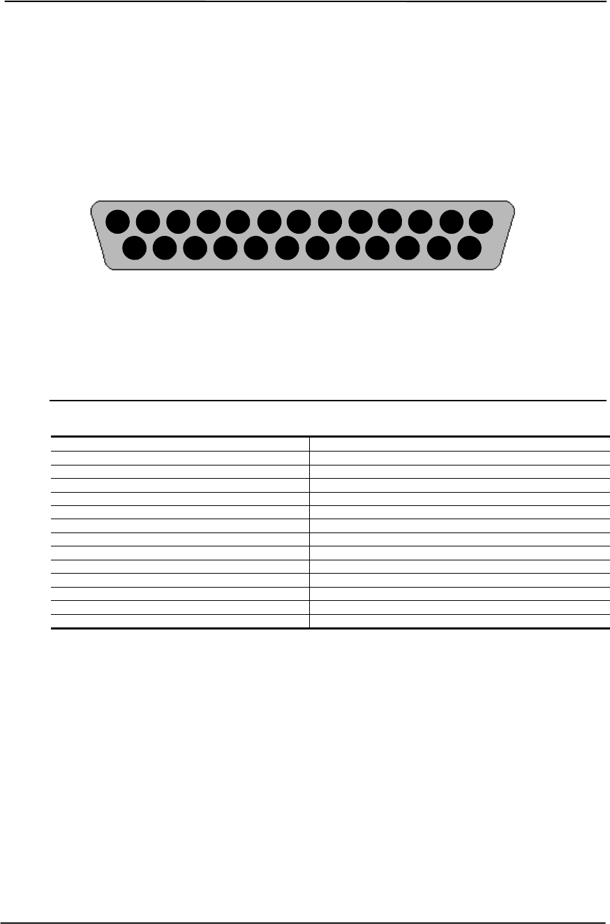
Technical Reference Guide
Compaq Deskpro EXS and Workstation 300 Personal Computers
Featuring the Intel Pentium 4 Processor
First Edition - December 2000
5-15
5.5.5 PARALLEL INTERFACE CONNECTOR
Figure 5-4 and Table 5-12 show the connector and pinout of the parallel interface connector. Note
that some signals are redefined depending on the port’s operational mode.
Figure 5-4. Parallel Interface Connector (Female DB-25 as viewed from rear of chassis)
Table 5–12. DB-25 Parallel Connector Pinout
Table 5-12.
DB-25 Parallel Connector Pinout
Pin Signal Function Pin Signal Function
1 STB- Strobe / Write [1] 14 LF- Line Feed [2]
2 D0 Data 0 15 ERR- Error [3]
3 D1 Data 1 16 INIT- Initialize Paper [4]
4 D2 Data 2 17 SLCTIN- Select In / Address. Strobe [1]
5 D3 Data 3 18 GND Ground
6 D4 Data 4 19 GND Ground
7 D5 Data 5 20 GND Ground
8 D6 Data 6 21 GND Ground
9 D7 Data 7 22 GND Ground
10 ACK- Acknowledge / Interrupt [1] 23 GND Ground
11 BSY Busy / Wait [1] 24 GND Ground
12 PE Paper End / User defined [1] 25 GND Ground
13 SLCT Select / User defined [1] -- -- --
NOTES: [1] Standard and ECP mode function / EPP mode function
[2] EPP mode function: Data Strobe
ECP modes: Auto Feed or Host Acknowledge
[3] EPP mode: user defined
ECP modes:Fault or Peripheral Req.
[4] EPP mode: Reset
ECP modes: Initialize or Reverse Req.
25 24 23 22 21 20 19 18 17 16 15 14
13 12 11 10 9 8 7 6 5 4 3 2 1

Chapter 5 Input/Output Interfaces
5-16 Compaq Deskpro EXS and Workstation 300 Personal Computers
Featuring the Intel Pentium 4 Processor
First Edition – December 2000
5.6 KEYBOARD/POINTING DEVICE INTERFACE
The keyboard/pointing device interface function is provided by the LPC47B357 I/O controller
component, which integrates 8042-compatible keyboard controller logic (hereafter referred to as
simply the “8042”) to communicate with the keyboard and pointing device using bi-directional
serial data transfers. The 8042 handles scan code translation and password lock protection for the
keyboard as well as communications with the pointing device. This section describes the interface
itself. The keyboard is discussed in the Appendix C.
5.6.1 KEYBOARD INTERFACE OPERATION
The data/clock link between the 8042 and the keyboard is uni-directional for Keyboard Mode 1
and bi-directional for Keyboard Modes 2 and 3. (These modes are discussed in detail in Appendix
C). This section describes Mode 2 (the default) mode of operation.
Communication between the keyboard and the 8042 consists of commands (originated by either
the keyboard or the 8042) and scan codes from the keyboard. A command can request an action or
indicate status. The keyboard interface uses IRQ1 to get the attention of the CPU.
The 8042 can send a command to the keyboard at any time. When the 8042 wants to send a
command, the 8042 clamps the clock signal from the keyboard for a minimum of 60 us. If the
keyboard is transmitting data at that time, the transmission is allowed to finish. When the 8042 is
ready to transmit to the keyboard, the 8042 pulls the data line low, causing the keyboard to
respond by pulling the clock line low as well, allowing the start bit to be clocked out of the 8042.
The data is then transferred serially, LSb first, to the keyboard (Figure 5-6). An odd parity bit is
sent following the eighth data bit. After the parity bit is received, the keyboard pulls the data line
low and clocks this condition to the 8042. When the keyboard receives the stop bit, the clock line
is pulled low to inhibit the keyboard and allow it to process the data.
Parameter Minimum Maximum
Tcy (Cycle Time) 0 us 80 us
Tcl (Clock Low) 25 us 35 us
Tch (Clock High) 25 us 45 us
Th (Data Hold) 0 us 25 us
Tss (Stop Bit Setup) 8 us 20 us
Tsh (Stop Bit Hold) 15 us 25 us
Figure 5-6. 8042-To-Keyboard Transmission of Code EDh, Timing Diagram
Start
Bit D0
(LSb)
D1 D2 D3 D4 D5 D6 D7
(MSb)
Parity Stop
Bit
01011011110
Data
Clock
Th Tcl TchTcy Tss Tsh

Technical Reference Guide
Compaq Deskpro EXS and Workstation 300 Personal Computers
Featuring the Intel Pentium 4 Processor
First Edition - December 2000
5-17
Control of the data and clock signals is shared by the 8042and the keyboard depending on the
originator of the transferred data. Note that the clock signal is always generated by the keyboard.
After the keyboard receives a command from the 8042, the keyboard returns an ACK code. If a
parity error or timeout occurs, a Resend command is sent to the 8042.
Table 5-13 lists and describes commands that can be issued by the 8042 to the keyboard.
Table 5–13. 8042-To-Keyboard Commands
Table 5-13.
8042-To-Keyboard Commands
Command Value Description
Set/Reset Status Indicators EDh Enables LED indicators. Value EDh is followed by an
option byte that specifies the indicator as follows:
Bits <7..3> not used
Bit <2>, Caps Lock (0 = off, 1 = on)
Bit <1>, NUM Lock (0 = off, 1 = on)
Bit <0>, Scroll Lock (0 = off, 1 = on)
Echo EEh Keyboard returns EEh when previously enabled.
Invalid Command EFh/F1
hThese commands are not acknowledged.
Select Alternate Scan Codes F0h Instructs the keyboard to select another set of scan codes
and sends an option byte after ACK is received:
01h = Mode 1
02h = Mode 2
03h = Mode 3
Read ID F2h Instructs the keyboard to stop scanning and return two
keyboard ID bytes.
Set Typematic Rate/Display F3h Instructs the keyboard to change typematic rate and delay
to specified values:
Bit <7>, Reserved - 0
Bits <6,5>, Delay Time
00 = 250 ms
01 = 500 ms
10 = 750 ms
11 = 1000 ms
Bits <4..0>, Transmission Rate:
00000 = 30.0 ms
00001 = 26.6 ms
00010 = 24.0 ms
00011 = 21.8 ms
:
11111 = 2.0 ms
Enable F4h Instructs keyboard to clear output buffer and last
typematic key and begin key scanning.
Default Disable F5h Resets keyboard to power-on default state and halts
scanning pending next 8042 command.
Set Default F6h Resets keyboard to power-on default state and enable
scanning.
Set Keys - Typematic F7h Clears keyboard buffer and sets default scan code set. [1]
Set Keys - Make/Brake F8h Clears keyboard buffer and sets default scan code set. [1]
Set Keys - Make F9h Clears keyboard buffer and sets default scan code set. [1]
Set Keys - Typematic/Make/Brake FAh Clears keyboard buffer and sets default scan code set. [1]
Set Type Key - Typematic FBh Clears keyboard buffer and prepares to receive key ID. [1]
Set Type Key - Make/Brake FCh Clears keyboard buffer and prepares to receive key ID. [1]
Set Type Key - Make FDh Clears keyboard buffer and prepares to receive key ID. [1]
Resend FEh 8042 detected error in keyboard transmission.
Reset FFh Resets program, runs keyboard BAT, defaults to Mode 2.
Note: [1] Used in Mode 3 only.

Chapter 5 Input/Output Interfaces
5-18 Compaq Deskpro EXS and Workstation 300 Personal Computers
Featuring the Intel Pentium 4 Processor
First Edition – December 2000
5.6.2 POINTING DEVICE INTERFACE OPERATION
The pointing device (typically a mouse) connects to a 6-pin DIN-type connector that is identical to
the keyboard connector both physically and electrically. The operation of the interface (clock and
data signal control) is the same as for the keyboard. The pointing device interface uses the IRQ12
interrupt.
5.6.3 KEYBOARD/POINTING DEVICE INTERFACE PROGRAMMING
Programming the keyboard interface consists of configuration, which occurs during POST, and
control, which occurs during runtime.
5.6.3.1 8042 Configuration
The keyboard/pointing device interface must be enabled and configured for a particular speed
before it can be used. Enabling and speed parameters of the 8042 logic are affected through the
PnP configuration registers of the LPC47B357 I/O controller. Enabling and speed control are
automatically set by the BIOS during POST but can also be accomplished with the Setup utility
and other software.
The keyboard interface configuration registers are listed in the following table:
Table 5–14. Keyboard Interface Configuration Registers
Table 5-14.
Keyboard Interface Configuration Registers
Index
Address Function R/W
30h Activate R/W
70h Primary Interrupt Select R/W
72h Secondary Interrupt Select R/W
F0h Reset and A20 Select R/W

Technical Reference Guide
Compaq Deskpro EXS and Workstation 300 Personal Computers
Featuring the Intel Pentium 4 Processor
First Edition - December 2000
5-19
5.6.3.2 8042 Control
The BIOS function INT 16 is typically used for controlling interaction with the keyboard. Sub-
functions of INT 16 conduct the basic routines of handling keyboard data (i.e., translating the
keyboard’s scan codes into ASCII codes). The keyboard/pointing device interface is accessed by
the CPU through I/O mapped ports 60h and 64h, which provide the following functions:
♦ Output buffer reads
♦ Input buffer writes
♦ Status reads
♦ Command writes
Ports 60h and 64h can be accessed using the IN instruction for a read and the OUT instruction for
a write. Prior to reading data from port 60h, the “Output Buffer Full” status bit (64h, bit <0>)
should be checked to ensure data is available. Likewise, before writing a command or data, the
“Input Buffer Empty” status bit (64h, bit <1>) should also be checked to ensure space is available.
I/O Port 60h
I/O port 60h is used for accessing the input and output buffers. This register is used to send and
receive data from the keyboard and the pointing device. This register is also used to send the
second byte of multi-byte commands to the 8042 and to receive responses from the 8042 for
commands that require a response.
A read of 60h by the CPU yields the byte held in the output buffer. The output buffer holds data
that has been received from the keyboard and is to be transferred to the system.
A CPU write to 60h places a data byte in the input byte buffer and sets the CMD/ DATA bit of the
Status register to DATA. The input buffer is used for transferring data from the system to the
keyboard. All data written to this port by the CPU will be transferred to the keyboard except bytes
that follow a multibyte command that was written to 64h
I/O Port 64h
I/O port 64h is used for reading the status register and for writing commands. A read of 64h by the
CPU will yield the status byte defined as follows:
Bit Function
7..4 General Purpose Flags.
3 CMD/DATA Flag (reflects the state of A2 during a CPU
write).
0 = Data
1 = Command
2 General Purpose Flag.
1 Input Buffer Full. Set (to 1) upon a CPU write. Cleared by
IN A, DBB instruction.
0 Output Buffer Full (if set). Cleared by a CPU read of the
buffer.
A CPU write to I/O port 64h places a command value into the input buffer and sets the
CMD/DATA bit of the status register (bit <3>) to CMD.

Chapter 5 Input/Output Interfaces
5-20 Compaq Deskpro EXS and Workstation 300 Personal Computers
Featuring the Intel Pentium 4 Processor
First Edition – December 2000
Table 5-15 lists the commands that can be sent to the 8042 by the CPU. The 8042 uses IRQ1 for
gaining the attention of the CPU.
Table 5–15. CPU Commands To The 8042
Table 5-15.
CPU Commands To The 8042
Value Command Description
20h Put current command byte in port 60h.
60h Load new command byte.
A4h Test password installed. Tests whether or not a password is installed in the 8042:
If FAh is returned, password is installed.
If F1h is returned, no password is installed.
A5h Load password. This multi-byte operation places a password in the 8042 using the following manner:
1. Write A5h to port 64h.
2. Write each character of the password in 9-bit scan code (translated) format to port 60h.
3. Write 00h to port 60h.
A6h Enable security. This command places the 8042 in password lock mode following the A5h
command. The correct password must then be entered before further communication with the 8042
is allowed.
A7h Disable pointing device. This command sets bit <5> of the 8042 command byte, pulling the clock
line of the pointing device interface low.
A8h Enable pointing device. This command clears bit <5> of the 8042 command byte, activating the
clock line of the pointing device interface.
A9h Test the clock and data lines of the pointing device interface and place test results in the output
buffer.
00h = No error detected
01h = Clock line stuck low
02h = Clock line stuck high
03h = Data line stuck low
04h = Data line stuck high
AAh Initialization. This command causes the 8042 to inhibit the keyboard and pointing device and places
55h into the output buffer.
ABh Test the clock and data lines of the keyboard interface and place test results in the output buffer.
00h = No error detected
01h = Clock line stuck low
02h = Clock line stuck high
03h = Data line stuck low
04h = Data line stuck high
ADh Disable keyboard command (sets bit <4> of the 8042 command byte).
AEh Enable keyboard command (clears bit <4> of the 8042 command byte).
C0h Read input port of the 8042. This command directs the 8042 to transfer the contents of the input port
to the output buffer so that they can be read at port 60h.
C2h Poll Input Port High. This command directs the 8042 to place bits <7..4> of the input port into the
upper half of the status byte on a continous basis until another command is received.
C3h Poll Input Port Low. This command directs the 8042 to place bits <3..0> of the input port into the
lower half of the status byte on a continous basis until another command is received.
D0h Read output port. This command directs the 8042 to transfer the contents of the output port to the
output buffer so that they can be read at port 60h.
D1h Write output port. This command directs the 8042 to place the next byte written to port 60h into the
output port (only bit <1> can be changed).
D2h Echo keyboard data. Directs the 8042 to send back to the CPU the next byte written to port 60h as if
it originated from the keyboard. No 11-to-9 bit translation takes place but an interrupt (IRQ1) is
generated if enabled.
D3h Echo pointing device data. Directs the 8042 to send back to the CPU the next byte written to port
60h as if it originated from the pointing device. An interrupt (IRQ12) is generated if enabled.
D4h Write to pointing device. Directs the 8042 to send the next byte written to 60h to the pointing device.
E0h Read test inputs. Directs the 8042 to transfer the test bits 1 and 0 into bits <1,0> of the output buffer.
F0h-
FFh Pulse output port. Controls the pulsing of bits <3..0> of the output port (0 = pulse, 1 = don’t pulse).
Note that pulsing bit <0> will reset the system.

Technical Reference Guide
Compaq Deskpro EXS and Workstation 300 Personal Computers
Featuring the Intel Pentium 4 Processor
First Edition - December 2000
5-21
5.6.4 KEYBOARD/POINTING DEVICE INTERFACE CONNECTOR
The legacy-light model provides separate PS/2 connectors for the keyboard and pointing device.
Both connectors are identical both physically and electrically. Figure 5-6 and Table 5-16 show the
connector and pinout of the keyboard/pointing device interface connectors.
Figure 5-5. Keyboard or Pointing Device Interface Connector
(PS/2 female as viewed from rear of chassis)
Table 5–16. Keyboard/Pointing Device Connector Pinout
Table 5-16.
Keyboard/Pointing Device Connector Pinout
Pin Signal Description Pin Signal Description
1 DATA Data 4 + 5 VDC Power
2 NC Not Connected 5 CLK Clock
3 GND Ground 6 NC Not Connected
6
5
2
4
3
1
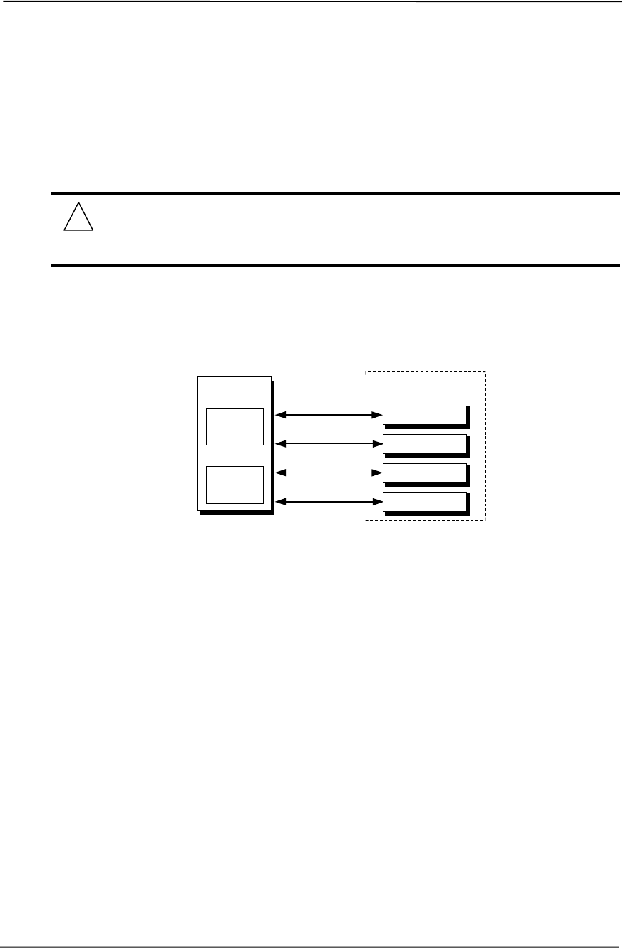
Chapter 5 Input/Output Interfaces
5-22 Compaq Deskpro EXS and Workstation 300 Personal Computers
Featuring the Intel Pentium 4 Processor
First Edition – December 2000
5.7 UNIVERSAL SERIAL BUS INTERFACE
The Universal Serial Bus (USB) interface provides asynchronous/isochronous data transfers of up
to 12 Mb/s with compatible peripherals such as keyboards, printers, or modems. This high-speed
interface supports hot-plugging of compatible devices, making possible system configuration
changes without powering down or even rebooting systems.
NOTE: It is recommended to run the Windows 98 (or later) operating system when
using USB peripherals, especially a USB keyboard and USB mouse. Problems may be
encountered when using USB devices with a system running Windows 95, although
some peripherals may operate satisfactorily.
As shown in Figure 5-7, the USB interface is provided by the 82801 ICH2 component and a USB
hub component. All models provide four series-A USB ports on the rear panel. For more
information on the USB interface refer to the following web site:
http://www.usb.org
Figure 5-6. USB I/F, Block Diagram
5.7.1 USB DATA FORMATS
The USB I/F uses non-return-to-zero inverted (NRZI) encoding for data transmissions, in which a
1 is represented by no change (between bit times) in signal level and a 0 is represented by a change
in signal level. Bit stuffing is employed prior to NRZ1 encoding so that in the event a string of 1’s
is transmitted (normally resulting in a steady signal level) a 0 is inserted after every six consecutive
1’s to ensure adequate signal transitions in the data stream.
82801
ICH2
Rear Panel
Tx/Rx Data
USB
I/F #2
USB Port C
USB Port D
Tx/Rx Data
Tx/Rx Data
USB
I/F #1
USB Port A
USB Port B
Tx/Rx Data

Technical Reference Guide
Compaq Deskpro EXS and Workstation 300 Personal Computers
Featuring the Intel Pentium 4 Processor
First Edition - December 2000
5-23
The USB transmissions consist of packets using one of four types of formats (Figure 5-8) that
include two or more of seven field types.
♦ Sync Field – 8-bit field that starts every packet and is used by the receiver to align the
incoming signal with the local clock.
♦ Packet Identifier (PID) Field – 8-bit field sent with every packet to identify the attributes (in.
out, start-of-frame (SOF), setup, data, acknowledge, stall, preamble) and the degree of error
correction to be applied.
♦ Address Field – 7-bit field that provides source information required in token packets.
♦ Endpoint Field – 4-bit field that provides destination information required in token packets.
♦ Frame Field – 11-bit field sent in Start-of-Frame (SOF) packets that are incremented by the
host and sent only at the start of each frame.
♦ Data Field – 0-1023-byte field of data.
♦ Cyclic Redundancy Check (CRC) Field – 5- or 16-bit field used to check transmission
integrity.
Figure 5-7. USB Packet Formats
Data is transferred LSb first. A cyclic redundancy check (CRC) is applied to all packets (except a
handshake packet). A packet causing a CRC error is generally completely ignored by the receiver.
Token Packet
SOF Packet
Data Packet
Handshake Packet
PID Field
(8 bits) Addr.
Field
(7 bit )
ENDP.
Field
(4 bit )
CRC Field
(5 bits)
Sync Field
(8 bits)
PID Field
(8 bits) Frame Field
(11 bits) CRC Field
(5 bits)
Sync Field
(8 bits)
PID Field
(8 bits) Data Field
(0-1023 bytes) CRC Field
(16 bits)
Sync Field
(8 bits)
PID Field
(8 bits)
Sync Field
(8 bits)

Chapter 5 Input/Output Interfaces
5-24 Compaq Deskpro EXS and Workstation 300 Personal Computers
Featuring the Intel Pentium 4 Processor
First Edition – December 2000
5.7.2 USB PROGRAMMING
Programming the USB interface consists of configuration, which typically occurs during POST,
and control, which occurs at runtime.
5.7.2.1 USB Configuration
The USB interface operates as a PCI device (31) within the 82801 ICH2 component (functions 2
and 4) and is configured using PCI Configuration Registers as listed in Table 5-17.
Table 5–17. USB Interface Configuration Registers
Table 5-17.
USB Interface Configuration Registers
PCI
Config.
Addr. Register Reset
Value
PCI
Config.
Addr. Register Reset
Value
00, 01h Vender ID 8086h 0Eh Header Type 00h
02, 03h Device ID 2442h or 2444h 20-23h I/O Space Base Address 1
04, 05h PCI Command 0000h 2C, 2Dh Sub. Vender ID 00h
06, 07h PCI Status 0280h 3Ch Interrupt Line 00h
08h Revision ID 00h 3Dh Interrupt Pin 03h
09h Programming I/F 00h 60h Serial Bus Release No. 10h
0Ah Sub Class Code 03h C0, C1h USB Leg. Kybd./Ms. Cntrl. 2000h
0Bh Base Class Code 0Ch C4h USB Resume Enable 00h
5.7.2.2 USB Control
The USB is controlled through I/O registers as listed in table 5-18.
Table 5–18. USB Control Registers
Table 5-18.
USB Control Registers
I/O Addr. Register Default Value
00, 01h Command 0000h
02, 03h Status 0000h
04, 05h Interupt Enable 0000h
06, 07 Frame Number 0000h
08, 0B Frame List Base Address 0000h
0Ch Start of Frame Modify 40h
10, 11h Port 1 Status/Control 0080h
12, 13h Port 2 Status/Control 0080h
18h Test Data 00h

Technical Reference Guide
Compaq Deskpro EXS and Workstation 300 Personal Computers
Featuring the Intel Pentium 4 Processor
First Edition - December 2000
5-25
5.7.3 USB CONNECTOR
Four series-A connectors are accessible on the rear panel of the chassis.
Figure 5-8. Universal Serial Bus Connector
Table 5–19. USB Connector Pinout
Table 5-19.
USB Connector Pinout
Pin Signal Description Pin Signal Description
1 Vcc +5 VDC 3 USB+ Data (plus)
2 USB- Data (minus) 4 GND Ground
5.7.4 USB CABLE DATA
The recommended cable length between the host and the USB device should be no longer than
sixteen feet for full-channel (12 MB/s) operation, depending on cable specification (see following
table).
Table 5–20. USB Cable Length Data
Table 5-20.
USB Cable Length Data
Conductor Size Resistance Maximum Length
20 AWG 0.036 Ω16.4 ft (5.00 m)
22 AWG 0.057 Ω9.94 ft (3.03 m)
24 AWG 0.091 Ω6.82 ft (2.08 m)
26 AWG 0.145 Ω4.30 ft (1.31 m)
28 AWG 0.232 Ω2.66 ft (0.81 m)
NOTE: For sub-channel (1.5 MB/s) operation and/or when using sub-standard cable
shorter lengths may be allowable and/or necessary.
The shield, chassis ground, and power ground should be tied together at the host end but left
unconnected at the device end to avoid ground loops.
Color code: Signal Insulation color
Data + Green
Data - White
Vcc Red
Ground Black
12 34

Chapter 5 Input/Output Interfaces
5-26 Compaq Deskpro EXS and Workstation 300 Personal Computers
Featuring the Intel Pentium 4 Processor
First Edition – December 2000
5.8 AUDIO SUBSYSTEM
The systems covered in this guide come standard with an embedded Sound Blaster 128 audio
subsystem.
5.8.1 FUNCTIONAL ANALYSIS
A block diagram of the audio subsystem is shown in Figure 5-10. The Ensonic ES1373 Audio
Controller, operating off the PCI bus, accesses and controls a Cirrus Logic CS4297A Audio
Codec. The codec provides the analog-to-digital (ADC) and digital-to-analog (DAC) conversions
as well as the mixing functions. All control functions such as volume, audio source selection, and
sampling rate are controlled through software over the PCI bus through the ES1373 Audio
Controller. Control data and digital audio streams (record and playback) are transferred between
the Audio Controller and the Audio Codec over the AC97 Link Bus.
The analog stereo outputs from the codec are applied to a 3-watt mono amplifier that drives a 16-
ohm speaker.
The interfaces allowing connection to external audio devices include:
Mic In - This input uses a three-conductor (stereo) 1/8” phone jack that is specifically designed for
connection of a condenser microphone with an impedance of 10-K ohms. This is the default
recording input after a system reset.
Line In - This input uses a three-conductor (stereo) 1/8” phone jack that is specifically designed
for connection of a high-impedance (10k-ohm) audio source such as a tape deck.
Headphones / Line / SPDIF Out - This output uses a three-conductor (stereo) 1/8” phone jack
that is designed for connecting a set of 16-ohm (nom.) stereo headphones or powered speakers.
Plugging into the Headphones jack mutes the signal to the internal speaker. This jack also provides
a digital output signal conforming to the Sony/Philips Digital Interface (SPDIF) format.
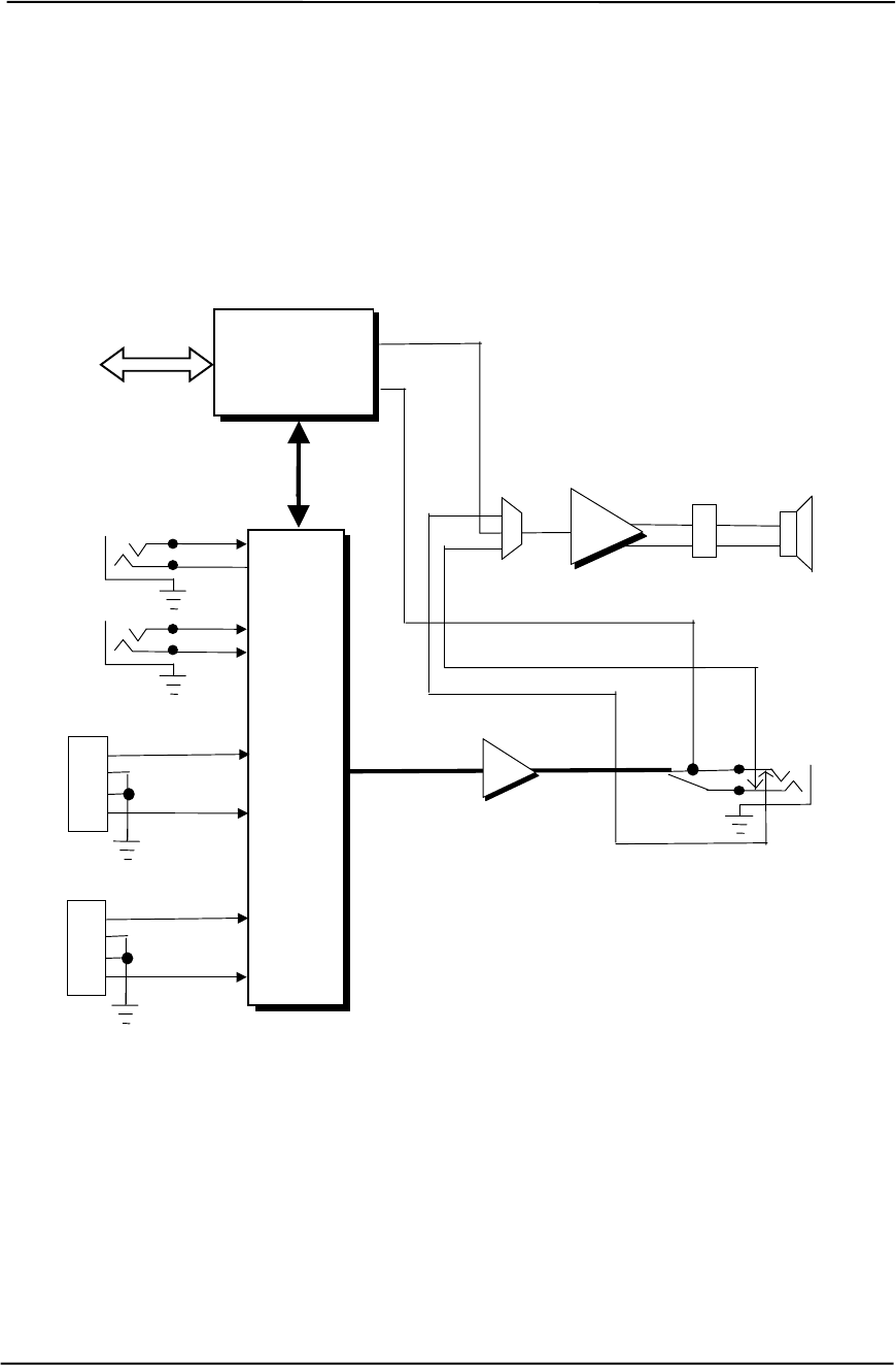
Technical Reference Guide
Compaq Deskpro EXS and Workstation 300 Personal Computers
Featuring the Intel Pentium 4 Processor
First Edition - December 2000
5-27
Figure 5-9. Audio Subsystem Functional Block Diagram
Headphones/
SPDIF/
Line Out
(L)
(R)
Line Out
Audio (L/R)
CS4297A
Audio
Codec
(L)
(R)
Line In
Mic In
Audio
Bias
Internal
Speaker
+
-
L / R
Audio
PC Beep Audio
AC97
Link Bus
ES1373
Audio
Controller
PCI Bus
ICH2
CD Audio (L)
CD Audio (R)
CD ROM
Header P7
1
2
3
4
Aux Audio (L)
Aux Audio (R)
Aux.
Header P11
1
2
3
4
Σ
Int. Speaker
Header P6
TDA
7056
(L)
(R)
SPDIF Out
1
2

Chapter 5 Input/Output Interfaces
5-28 Compaq Deskpro EXS and Workstation 300 Personal Computers
Featuring the Intel Pentium 4 Processor
First Edition – December 2000
5.8.2 AUDIO CONTROLLER
The Creative Technology, Ltd. Ensoniq ES1373 Audio Controller is a PCI device that includes the
following features:
♦ Compatible with software written for Sound Blaster 128
♦ 64-Voice wavetable synthesizer
♦ 4000+ sound library
♦ Tone control and speaker equalization
♦ Multiple sampling rate support up to 48 KHz
♦ OPL-FM and MPU-401 emulation support
♦ Supports Ensoniq’s 3D Positional Audio algorithm
♦ Aureal A3D API support
♦ Microsoft DirectSound, DirectSound 3D, DirectMusic support
♦ DOS game compatibility
♦ AC’97 Link Bus
♦ S/PDIF output
♦ ACPI power management
The ES1373 audio controller operates as a PCI bus master and slave device that includes an
integrated cache designed to handle the memory bandwidth requirements of audio processing.
System memory is accessed as required to keep output cache full (during playback) and input
cache (relatively) empty (during record) in accordance with the needs of the audio codec. The
integrated cache memory stores playback/record data, sample rate converter data, and control
register data. A virtual 3-channel DMA controller handles cache memory operations.
The control registers are accessed using programmed I/O on the PCI bus. All register reads are
done as long words, while register writes are performed in byte word or long word format.
In addition to the AC’97 link bus, the audio controller provides a Sony/Philips Digital Interface
(SPDIF) output that is applied to the tip connection of the headphone/line out jack. The SPDIF
signal format (also known as IEC-958) is a stereo digital signal specification becoming common to
consumer products.
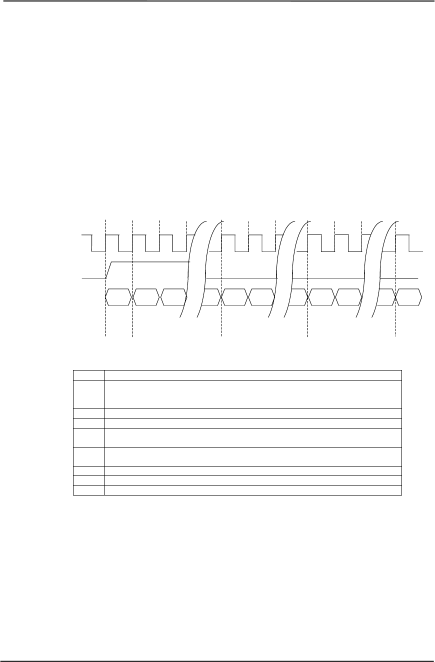
Technical Reference Guide
Compaq Deskpro EXS and Workstation 300 Personal Computers
Featuring the Intel Pentium 4 Processor
First Edition - December 2000
5-29
5.8.3 AC97 LINK BUS
The audio controller and the audio codec communicate over a five-signal AC97 Link Bus (Figure
5-12). The AC97 Link Bus includes two serial data lines (SD OUT/SD IN) that transfer control
and PCM audio data serially to and from the audio codec using a time-division multiplexed (TDM)
protocol. The data lines are qualified by a 12.288 MHz BIT_CLK signal driven by the audio
codec. Data is transferred in frames synchronized by the 48-KHz SYNC signal, which is derived
from the clock signal and driven by the audio controller. The SYNC signal is high during the
frame’s tag phase then falls during T17and remains low during the data phase. A frame consists of
one 16-bit tag slot followed by twelve 20-bit data slots. When asserted (typically during a power
cycle), the RESET- signal (not shown) will reset all audio registers to their default values.
Slot Description
0 Bit 15: Frame valid bit
Bits 14-3: Slots 1-12 valid bits
Bits 2-0: Codec ID
1 Command address: Bit 19, R/W; Bits 18..12, reg. Index; Bits 11..0, reserved.
2 Command data
3 Bits 19-4: PCM audio data, left channel (SD OUT, playback; SD IN, record)
Bits 3-0 all zeros
4 Bits 19-4: PCM audio data, right channel (SD OUT, playback; SD IN, record)
Bits 3-0 all zeros
5 Modem codec data (not used in this system)
6-11 Reserved
12 I/O control
Figure 5-10. AC’97 Link Bus Protocol
Bit 0 Bit 0 Bit 0
T1 T2
3
BIT_CLK
(12.288 MHz)
Codec
Ready Bit 19 Bit 18 Bit 19 Bit 18 Bit 19
SYNC
(48 KHz)
SD OUT
or SD IN
T18 T19 T38 T39 T58
Slot 0
(Tag) Slot 1
(Data) Slot 2
(Data)
Bit 15 Bit 14
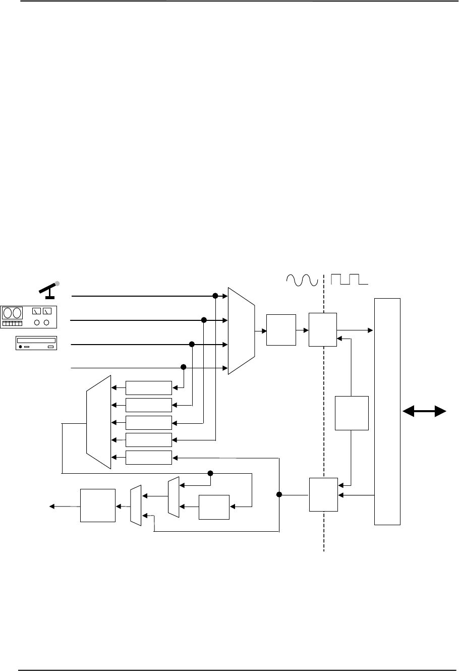
Chapter 5 Input/Output Interfaces
5-30 Compaq Deskpro EXS and Workstation 300 Personal Computers
Featuring the Intel Pentium 4 Processor
First Edition – December 2000
5.8.4 AUDIO CODEC
The Cirrus Logic CS4297A audio codec provides pulse code modulation (PCM) coding and
decoding of audio information as well as the selection and/or mixing of analog channels. As shown
in Figure 5-11, analog audio from a microphone, tape, or CD can be selected and, if to be recorded
(saved) onto a disk drive, routed through an analog-to-digital converter (ADC). The resulting left
and right PCM record data are muxed into a time-division-multiplexed (TDM) data stream (SD IN
signal) that is routed to the audio controller. Playback (PB) audio takes the reverse path from the
audio controller to the audio codec as SD OUT data and is decoded and processed by the digital-
to-analog converter (DAC). The codec supports simultaneous record and playback of stereo (left
and right) audio. The Sample Rate Generator may be set for sampling frequencies up to 48 KHz.
Analog audio may then be routed through 3D stereo enhancement processor or bypassed to the
output selector (SEL). The integrated analog mixer provides the computer control-console
functionality handling multiple audio inputs.
Figure 5-11. CS4297A Audio Codec Functional Block Diagram
All inputs and outputs are two-channel stereo except for the microphone input, which is inputted as
a single-channel but mixed internally onto both left and right channels. The microphone input is
the default active input. All block functions are controlled through index-addressed registers of the
codec.
Output
Amps
Sample
Rate
Gen.
Audio
Format
AC97
Link
I/F
Rec.
Input
Select
Mic In
Line In
CD In
Audio
Controller
Rec
Gain/
Mute
3D
Proc.
Audio S
E
L
ADC
Rec
Data
PB
Data
AC97
Link Bus
Master
Gain/
Mute
Aux In
S
E
L
Σ/
Mixer
Gain/Mute
Gain/Mute
Gain/Mute
Gain/Mute
Gain/Mute
DAC

Technical Reference Guide
Compaq Deskpro EXS and Workstation 300 Personal Computers
Featuring the Intel Pentium 4 Processor
First Edition - December 2000
5-31
5.8.5 AUDIO PROGRAMMING
Audio subsystem programming consists configuration, typically accomplished during POST, and
control, which occurs during runtime.
5.8.5.1 Audio Configuration
The audio subsystem is configured according to PCI protocol through the ES1373 audio controller.
Table 5-21 lists the PCI configuration registers of the audio subsystem.
Table 5–21. AC’97 Audio Controller PCI Configuration Registers
Table 5-21.
AC’97 Audio Controller
PCI Configuration Registers
PCI
Conf.
Addr. Register
Value
on
Reset
PCI
Conf.
Addr. Register
Value
on
Reset
00-01h Vender ID 1274h 14-17h Native Audio Bus Mstr. Addr. 0’s
02-03h Device ID 1373h 18-1Bh Reserved 0’s
04-05h PCI Command 0000h 1C-2Bh Reserved 0’s
06-07h PCI Status X610h 2C-2Dh Subsystem Vender ID 1274h
08h Revision ID 00h 2E-2Fh Subsystem ID 1373h
09h Programming 00h 30h Exp. ROM Addr. 0’s
0Ah Sub-Class 01h 34h Capabilities Pointer DCh
0Bh Base Class Code 04h 3Ch Interrupt Line xxh
0Eh Header Type 00h 3Dh Interrupt Pin 01h
10-13h Native Audio Mixer Base Addr. 1 3E, 3Fh Min. GNT/Min, LAT 800Ch
5.8.5.2 Audio Control
The audio subsystem is controlled through a set of indexed registers that physically reside in the
audio codec . The register addresses are decoded by the audio controller and forwarded to the
audio codec over the AC97 Link Bus previously described. The audio codec’s control registers
(Table 5-22) are mapped into 64 kilobytes of variable I/O space.
Table 5–22. AC’97 Audio Codec Control Registers
Table 5-22.
AC’97 Audio Codec Control Registers
Offset
Addr. / Register
Value
On
Reset Offset
Addr. / Register
Value
On
Reset Offset
Addr. / Register
Value
On
Reset
00h Reset 0100h 14h Video Vol. 8808h 28h Ext. Audio ID. 0001h
02h Master Vol. 8000h 16h Aux Vol. 8808h 2Ah Ext. Audio Ctrl/Sts 0000h
04h Reserved X 18h PCM Out Vol. 8808h 2Ch PCM DAC SRate BB80h
06h Mono Mstr. Vol. 8000h 1Ah Record Sel. 0000h 32h PCM ADC SRate BB80h
08h Reserved X 1Ch Record Gain 8000h 5Eh AC Mode Control 0080h
0Ah PC Beep Vol. 8000h 1Eh Reserved X 60h Misc. Cystal Cntrl. 0023h
0Ch Phone In Vol. 8008h 20h Gen. Purpose 0000h 68h S/PDIF Cntrl. 0000h
0Eh Mic Vol. 8008h 22h 3D Control 0000h -- --
10h Line In Vol. 8808h 24h Reserved X 7Ch Vender ID1 4352h
12h CD Vol. 8808h 26h Pwr Mgnt. 000xh 7Eh Vender ID2 5931h

Chapter 5 Input/Output Interfaces
5-32 Compaq Deskpro EXS and Workstation 300 Personal Computers
Featuring the Intel Pentium 4 Processor
First Edition – December 2000
5.8.6 AUDIO SPECIFICATIONS
The specifications for the audio subsystem are listed in Table 5-23.
Table 5–23. Audio Subsystem Specifications
Table 5-23.
Audio Subsystem Specifications
Paramemter Measurement
Sampling Rate 5.51 KHz to 48 KHz
Resolution 16 bit
Nominal Input Voltage:
Mic In (w/+20 db gain)
Line In 0.1 Vrms
1.0 Vrms
Impedance:
Mic In
Line In
Line Out (codec output)
1 K ohms (nom)
10 K ohms (min)
730 ohms
Signal-to-Noise Ratio (input to Line Out) 70 db (nom)
Max. Power Output (with 10% THD): 3 watts (into 16 ohms)
Input Gain Attenuation Range 46.5 db
Master Volume Range -94.5 db
Frequency Response:
Codec
Speaker 20-20 KHz
450 - 4000 Hz

Technical Reference Guide
Compaq Deskpro EXS and Workstation 300 Personal Computers
Featuring the Intel Pentium 4 Processor
First Edition - December 2000
5-33
5.9 NETWORK SUPPORT
These systems include specific features to support network interface PCI cards that may be
installed. These features, including network-alert functions with system-off support, are described
in the following subsections.
5.9.1 PCI VER. 2.2 SUPPORT
These systems support the Power Management Event (PME-) signal and provided 3.3 VDC
auxiliary power for all PCI slots. Network interface cards compliant with PCI specification ver. 2.2
may be installed to providE “system off” network support without additional cable connections. In
a powered-down state the compliant network card receives 3.3 volts of auxiliary DC power on pin
A14 of the PCI connector and uses PCI pin A19 for the PME- signal that is routed to general
purpose input #13 of the LPC47B357 I/O controller. Network activity causing the NIC card to
assert the PME- signal can be used to restart or “wake” the system from a suspend state.
NOTE: For auxiliary power to be available in a system-off condition the system unit
must be plugged into a live AC outlet. Controlling unit power through a switchable power
strip will, with the strip turned off, disable PME- functionality.
5.9.2 ALERT-ON-LAN SUPPORT
Alert-On-LAN (AOL) support allows a compliant network interface controller (NIC) card to
communicate the occurrence of certain events over a network even while the system unit is
powered off. In a system-off (powered down) condition a NIC card receives auxiliary +3.3 VDC
power (derived from the +5 VDC auxiliary power from the power supply assembly). Certain
events will result in a compliant NIC card to transmit an appropriate pre-constructed message over
the network to a system management console.
Reportable AOL events are listed in the following table:
Table 5–24. AOL Events
Table 5-24.
AOL Events
Event Description
BIOS Failure System fails to boot successfully.
OS Problem System fails to load operating system after POST.
Missing/Faulty Processor Processor fails to fetch first instruction.
Heartbeat Indication of system’s network presence (sent approximately every 30
seconds in normal operation).

Chapter 5 Input/Output Interfaces
5-34 Compaq Deskpro EXS and Workstation 300 Personal Computers
Featuring the Intel Pentium 4 Processor
First Edition – December 2000
As shown in the following figure, support with an AOL-compliant NIC PCI card (such as the Intel
PRO/100+ Management Adapter Solution) requires no auxiliary cable since the communication of
alert events is handled through the PCI bus interface.
Figure 5-12. AOL Implementation (Generic Representation)
The 82801 ICH initiates event notification by transmitting an alert message over the SMBus-type
Alert Clock/Alert Data interface to a NIC card. On these systems the Alert Clock/Alert Data
signals are wired-Or’d with the SMBus signals and use the SDONEn/SBOn signals lines for
routing to a NIC card on the PCI bus.
The ICH’s alert message will be the result of a signal from a sensor (thermal or CPU state) or from
the ICH’s detection of the system’s running status. Upon receiving the alert message from the ICH
the NIC transmits the appropriate, pre-constructed message over the network.
The AOL implementation requirements are as follows:
1. Intel PRO/100 network drivers 4.11 or later (available from Compaq).
2. Intel Alert-On-LAN Utilities, version 2.6 (available from Compaq).
3. Management console running one of the following:
a. HP OpenView Network Node Manager 6.x
b. Intel LANDesk Client Manager
c. Sample Application Console from the Intel AOL Utilities (item #2 above)
NIC Card in PCI Slot
System Board
82801 ICH2
Alert Clock Trace
Alert Data Trace
Network
Cable
Technical Reference Guide
Compaq Deskpro EXS and Workstation 300 Personal Computers
Featuring the Intel Pentium 4 Processor
First Edition - December 2000
5-35
5.9.3 REMOTE SYSTEM ALERT SUPPORT
These systems provide Remote System Alert (RSA) support for such NIC cards as the 3Com
3C905C-TX NIC card. The RSA function is similar to AOL in that the unit provides, even while
powered off, system status alert messages to a network console. However, NIC cards implementing
the RSA method do not use the SMBus for receiving alert information and therefore require, in
addition to the PCI connection, an auxiliary AOL/SOS cable connection with the system board
(Figure 5-13).
Figure 5-13. Remote Sense Alert Implementation (Generic Representation)
In the Remote Sense Alert implementation, a NIC card receives event notification directly from the
system’s thermal sensors and the LPC47B357 I/O controller over an AOL/SOS cable connection
(Figure 5-14). During system-off conditions the NIC card receives auxiliary power from the 3.3
VDC auxiliary power rail on the PCI bus.
Figure 5-14. RSA Logic, Block Diagram
NIC Card in PCI Slot
System Board
AOL/SOS Cable
Network
Cable AOL/SOS
Header P12
System Board NIC Card
PCI
Connector
Thermal
ASIC
PCI
Bus
PCI
Bus
7
BIOS Fail
OS Fail
Intrusion
Thermal
Fan Alert
Pwr Alert
47B357
I/O Cntlr.
NC
NC
AOL/SOS
Header1SOS
NC
NC

Chapter 5 Input/Output Interfaces
5-36 Compaq Deskpro EXS and Workstation 300 Personal Computers
Featuring the Intel Pentium 4 Processor
First Edition – December 2000
Reportable RSA events are listed in the following table:
Table 5–25. Remote System Alert Events
Table 5-25.
Remote System Alert Events
Event Description
BIOS Failure System fails to boot successfully.
Thermal Condition CPU Thermal shutdown reported.
Heartbeat Indication of system’s network presence (sent approximately every 30
seconds in normal operation).
The current Remote System Alert implementation requirements are as follows:
1. 3Com Etherlink 3C905C-TX NIC.
2. 7-pin AOL/SOS cable.
3. 3Com EtherDisk Driver 5.x or later (available from Compaq).
4. Client-side utility software (included with driver).
5. Server-side utility software (available from Compaq).
6. Management console running one of the following:
a. HP OpenView Network Node Manager 6.x
b. Intel LANDesk Client Manager
Technical Reference Guide
Compaq Deskpro EXS and Workstation 300 Personal Computers
Featuring the Intel Pentium 4 Processor
First Edition - December 2000
6-1
Drives
110/230 VAC
115/230 VAC
Select SW
Chapter 6
POWER and SIGNAL
DISTRIBUTION
6. Chapter 6 POWER SUPPLY AND DISTRIBUTION
6.1 INTRODUCTION
This chapter describes the power supply and method of general power and signal distribution.
Topics covered in this chapter include:
♦ Power supply assembly/control (6.2) page 6-1
♦ Power distribution (6.3) page 6-5
♦ Signal distribution (6.4) page 6-8
6.2 POWER SUPPLY ASSEMBLY/CONTROL
This system features a power supply assembly that is controlled through programmable logic
(Figure 6-1).
Figure 6–1. Power Distribution and Control, Block Diagram
Power Supply
Assembly
+5 VDC
-5 VDC
+12 VDC
-12 VDC
+5
AUX
CPU, Slots, Chipsets, Logic
& Voltage Regulators
PS
On
Fan
Off
+3.3
AUX
System Board
Power On/Off
Front Bezel
Power On
110 VAC
230 VAC
Mains
Fan
Spd
+5 VDC
+12 VDC
+12.8 VDC

Chapter 6 Power and Signal Distribution
Compaq Deskpro EXS and Workstation 300 Personal Computers
Featuring the Intel Pentium 4 Processor
First Edition - December 2000
6-2
6.2.1 POWER SUPPLY ASSEMBLY
The power supply assembly is contained in a single unit that features a selectable input voltage:
90-132 VAC and 180-264 VAC. Deskpro EN SFF systems use a 120-watt supply while all other
systems employ a 265-watt supply. Table 6-1 list the specifications of the power supplies.
Table 6–1. 265-Watt Power Supply Assembly Specifications
Table 6-1.
265-Watt Power Supply Assembly Specifications (P/N 195196)
Range/
Tolerance Min. Current
Loading [1] Max.
Current Surge
Current [2] Max.
Ripple
Input Line Voltage:
115 VAC Setting
230 VAC Setting 90 - 132 VAC
180-264 VAC --
-- --
-- --
-- --
--
Line Frequency 47 - 63 Hz -- -- -- --
Constant Input (AC) Current -- -- 4.0 A -- --
+3.3 VDC Output +/- 5% 1.00 A 24.0 A 24.0 A 50 mV
+5 VDC Output +/- 5 % 1.00 A 11.0 A 11.0 A 50 mV
+3 AUX Output +/- 5 % 0.00 A 2.20 A 2.20 A 50 mV
+5 AUX Output +/- 4 % 0.0 A 1.70 A 1.70 A 50 mV
+12 VDC Output +/- 5 % 0.00 A 5.00 A 8.0 A 120 mV
+12.8 VDC Output (Vcpu) +/- 5 % 0.00 A 7.50 A 10.5 A 200 mv
-12 VDC Output +/- 10 % 0.00 A 0.15 A 0.15 A 200 mV
NOTES: [1] Minimum loading requirements must be met at all times to ensure normal operation
and specification compliance.
[2] Surge duration no longer than 10 seconds and +12 tolerance +/- 10%.

Technical Reference Guide
Compaq Deskpro EXS and Workstation 300 Personal Computers
Featuring the Intel Pentium 4 Processor
First Edition - December 2000
6-3
6.2.2 POWER CONTROL
The power supply assembly is controlled digitally by the PS On signal (Figure 7-1). When PS On
is asserted, the Power Supply Assembly is activated and all voltage outputs are produced. When
PS On is de-asserted, the Power Supply Assembly is off and all voltages (except +3.3 AUX and +5
AUX) are not generated. Note that the +3.3 AUX and +5 AUX voltages are always produced
as long as the system is connected to a live AC source.
6.2.2.1 Power Button
The PS On signal is typically controlled through the Power Button which, when pressed and
released, applies a negative (grounding) pulse to the power control logic. The resultant action of
pressing the power button depends on the state and mode of the system at that time and is
described as follows:
System State Pressed Power Button Results In:
Off Negative pulse, of which the falling edge results in power control logic asserting PS
On signal to Power Supply Assembly, which then initializes. ACPI four-second
counter is not active.
On, ACPI Disabled Negative pulse, of which the falling edge causes power control logic to de-assert the
PS On signal. ACPI four-second counter is not active.
On, ACPI Enabled Pressed and Released Under Four Seconds:
Negative pulse, of which the falling edge causes power control logic to
generate SMI-, set a bit in the SMI source register, set a bit for button status,
and start four-second counter. Software should clear the button status bit
within four seconds and the Suspend state is entered. If the status bit is
not cleared by software in four seconds PS On is de-asserted and the
power supply assembly shuts down (this operation is meant as a guard if
the OS is hung).
Pressed and Held At least Four Seconds Before Release:
If the button is held in for at least four seconds and then released, PS On is
negated, de-activating the power supply.
6.2.2.2 System Board LED Indications
Three LEDs located on the system board (refer to chapter 2, figure 2-5) provide status and a means
to troubleshoot possible power-related problems.
System Board LED Figure 2-5
Item # Function
Power supply on / 5V aux 19 When illuminated, indicates system is plugged into a live AC outlet
but not turned on. When off and system is plugged into a live AC
outlet, indicates PS On is asserted (system turned on).
Power button pressed 22 Momentarily illuminates when the power button is pressed.
3.3V aux 25 When illuminated, indicates system is plugged into a live AC outlet.

Chapter 6 Power and Signal Distribution
Compaq Deskpro EXS and Workstation 300 Personal Computers
Featuring the Intel Pentium 4 Processor
First Edition - December 2000
6-4
6.2.2.3 Power LED Indications
A dual-color LED located on the front panel (bezel) is used to indicate system power status. The
front panel (bezel) power LED provides a visual indication of key system conditions listed as
follows:
Power LED Condition
Steady green Normal full-on operation
Blinks green @ 1 Hz Suspend state (S1)
Blinks green @ 2 Hz Sleep (suspend to RAM) state (S3)
Blinks green @ 4 Hz Sleep (suspend to disk) state (S4)
Steady red Processor not seated
Blinks red @ 0.5 Hz Power supply crowbar activated
Blinks red @ 1 Hz BIOS ROM error
Blinks red @ 4 Hz Thermal condition: processor has overheated and shut down
6.2.2.4 Wake Up Events
The PS On signal can be activated with a power “wake-up” of the system due to the occurrence of
a magic packet, serial port ring, or PCI power management (PME) event. These events can be
individually enabled through the Setup utility to wake up the system from a sleep (low power)
state.
NOTE: Wake-up functionality requires that certain circuits receive auxiliary power
while the system is turned off. The system unit must be plugged into a live AC outlet
for wake up events to function. Using an AC power strip to control system unit power
will disable wake-up event functionality.
The wake up sequence for each event occurs as follows:
Wake-On-LAN
The network interface controller (NIC) can be configured for detection of a “Magic Packet” and
wake the system up from sleep mode through the assertion of the PME- signal on the PCI bus.
Refer to Chapter 5, “Network Support” for more information.
Modem Ring
A ring condition on serial port A (COM1) or serial port B (COM2) can be detected by the power
control logic and, if so configured, cause the PS On signal to be asserted.
Power Management Event
A power management event that asserts the PME- signal on the PCI bus can be enabled to cause
the power control logic to generate the PS On. Note that the PCI card must be PCI ver. 2.2
compliant to support this function.
Technical Reference Guide
Compaq Deskpro EXS and Workstation 300 Personal Computers
Featuring the Intel Pentium 4 Processor
First Edition - December 2000
6-5
6.3 POWER DISTRIBUTION
6.3.1 3.3/5/12 VDC DISTRIBUTION
The power supply assembly includes a multi-connector cable assembly that routes +3.3 VDC, +5
VDC, -5 VDC, +12 VC, and -12 VDC to the system board as well as to the individual drive
assemblies. Figure 6-2 shows the power supply cabling for Deskpro EXS and Workstation 300
series units.
Conn. Pin 1 Pin 2 Pin 3 Pin 4 Pin 5 Pin 6 Pin 7 Pin 8 Pin 9 Pin 10 Pin 11 Pin 12
P1 +3.3 +3.3 RTN +5 RTN +5 AuxRtn FO +5 Aux +12 +3.3Aux FSpd
P1 [1] +3.3 -12 Rtn PS On RTN RSRTN RTN -3.3 +5 +5 +3.3RS FS
P2, 4-7 +5 GND GND +12
P3 GND GND +12.8 +12.8
NOTES: Connectors not shown to scale.
All + and - values are VDC.
RTN = Return (signal ground)
GND = Power ground
RS = Remote sense
FO = Fan off
FSpd = Fan speed
FS = Fan Sink
[1] This row represents pins 13-24 of connector P1.
Figure 6–2. Power Cable Diagram
P7
4 3 2 1
P1
1 1211 2 5 4 3 7 6
14
10
13
8 9
15 16 17 18 19 20 21 22 23 24
Power Supply
Assembly
(SP# 195196)
To
Drive
Assemblies
P1
P7
To
System
Board
P6
P4
P2
P5
P3 12
34
P3
1 2 3 4
P2-P6
Chapter 6 Power and Signal Distribution
Compaq Deskpro EXS and Workstation 300 Personal Computers
Featuring the Intel Pentium 4 Processor
First Edition - December 2000
6-6
6.3.2 LOW VOLTAGE PRODUCTION/DISTRIBUTION
Voltages less than 3.3 VDC including processor core (VccP) voltage are produced through
regulator circuitry on the system board.
Figure 6–3. Low Voltage Supply and Distribution Diagram
The VccP regulator produces the VccP (processor core) voltage according to the strapping of
signals VID4..0 by the processor. The possible voltages available are listed as follows:
VID 4..0 VccP VID 4..0 VccP VID 4..0 VccP
00000 2.05 VDC 01011 1.50 VDC 10110 2.90 VDC
00001 2.00 VDC 01100 1.45 VDC 10111 2.80 VDC
00010 1.95 VDC 01101 1.40 VDC 11000 2.70 VDC
00011 1.90 VDC 01110 1.35 VDC 11001 2.60 VDC
00100 1.85 VDC 01111 1.30 VDC 11010 2.50 VDC
00101 1.80 VDC 10000 3.50 VDC 11011 2.40 VDC
00110 1.75 VDC 10001 3.40 VDC 11100 2.30 VDC
00111 1.70 VDC 10010 3.30 VDC 11101 2.20 VDC
01000 1.65 VDC 10011 3.20 VDC 11110 2.10 VDC
01001 1.60 VDC 10100 3.10 VDC 11111 No CPU
01010 1.55 VDC 10101 3.00 VDC -- --
VccP (see text)
Regulator
Circuit
+12 VDC
VID0 Processor
VID1
VID2
VID3
Power Supply
+5 VDC
+3.3 VDC
+5 AUX
RIMMs
3.3
RIMM
Circuit
3.3 VDC
+3 AUX
RIMM
Power
Circuitry
2.5 S3 VDC
Processor
+1.8 VDC
+5 VDC
AGP
PWR VDDQ (1.5 VDC) AGP Bus
VID4
+12 VDC
+3.3 VDC
+1.4 Ref
RIMMs
+12.8 Vcpu
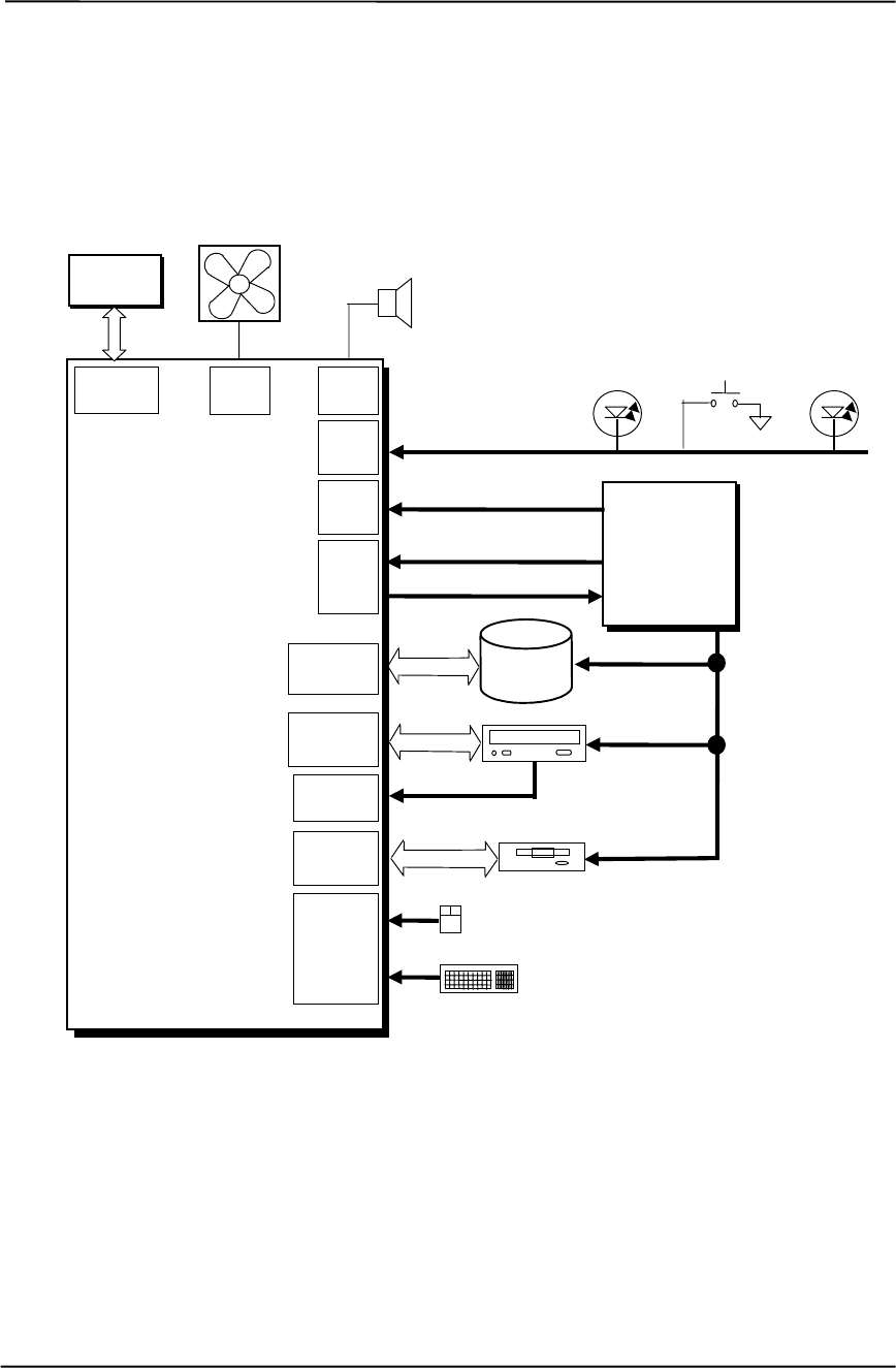
Technical Reference Guide
Compaq Deskpro EXS and Workstation 300 Personal Computers
Featuring the Intel Pentium 4 Processor
First Edition - December 2000
6-7
6.4 SIGNAL DISTRIBUTION
Figures 6-4 shows general signal distribution between the main subassemblies of the system units.
NOTES:
[1] See Figure 6-7 for header pinout.
Figure 6–4. Signal Distribution Diagram, Typical Configuration
System
Board
(PCA # 010821)
Power
Supply
Assembly
3/5/12 VDC, 3/5AUX
IDE
Data, Cntl
IDE
Hard Drive
5, 12 VDC
Conn.
P1
Pri. IDE
Conn. P20
Sec. IDE
Conn. P21
IDE I/F CD-ROM
Keyboard
Mouse
Dsk.
Conn. P10
Diskette Drive
Conn.
P5 [1]
5, 12 VDC
5, 12 VDC
Mouse
Kybd.
Conn. J68
AGP
Connector
Dskt.
Data, Cntl
AGP
Bus
Graphics
Controller
Conn.
P8
Fan
PWR
Fan Cntrl., PS On
Conn.
P6
Audio
Chassis Fan
Audio
Conn. P7
L/R Audio
HD Activity
Power On/Off
Power On
Pwr Btn, Pwr/HD LED
Conn.
P3 12.8 Vcpu
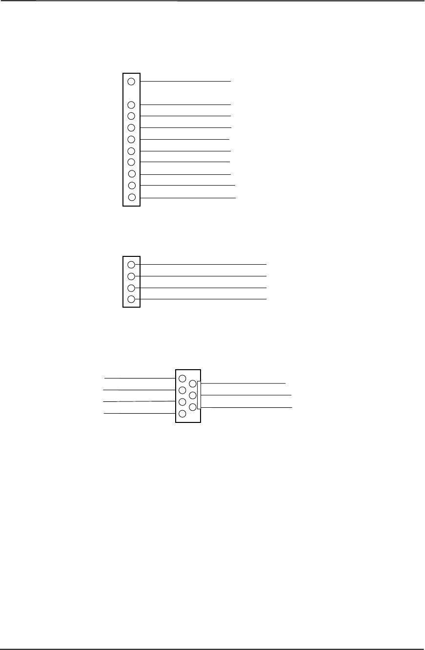
Chapter 6 Power and Signal Distribution
Compaq Deskpro EXS and Workstation 300 Personal Computers
Featuring the Intel Pentium 4 Processor
First Edition - December 2000
6-8
NOTE: No polarity consideration required for connection to speaker header P6 or SCSI HD LED header P29.
[1] Separate cable connection for these two pins (equivalent of header P29 on other systems).
Figure 6–5. Header Pinouts
CD ROM Audio Header P7
1 Audio (Left Channel)
3 Ground
4 Audio (right channel)
2 Ground
BIOS Fail 1
Not Connected 5
Ground 7
Not Connected 3 2 Not Connected
6 Thermal
4 Not Connected
AOL/SOS Header P12
1 HD LED anode
3 HD LED cathode
4 PWR LED anode
5 PWR LED cathode
6 PWR button (gnd)
7 PWR button (+)
8 Reserved
9 GND
Power Button/LED Header P5
10 SCSI HD LED [1]
11 SCSI HD LED [1]

Technical Reference Guide
Compaq Deskpro EXS and Workstation 300 Personal Computers
Featuring the Intel Pentium 4 Processor
First Edition - December 2000
7-1
Chapter 7
BIOS ROM
7. Chapter 7 BIOS ROM
7.1 INTRODUCTION
The Basic Input/Output System (BIOS) of the computer is a collection of machine language
programs stored as firmware in read-only memory (ROM). The BIOS ROM includes such
functions as Power-On Self Test (POST), PCI device initialization, Plug ‘n Play support, power
management activities, and the Setup utility. The firmware contained in the BIOS ROM supports
the following operating systems and specifications:
♦ DOS 6.2
♦ Windows 3.1 (and Windows for Workgroups 3.11)
♦ Windows 95, 98, and 2000
♦ Windows NT 3.5 and 4.0
♦ OS/2 ver 2.1 and OS/2 Warp
♦ SCO Unix
♦ DMI 2.1
♦ Intel Wired for Management (WfM) ver. 2.2
♦ Alert-On-LAN (AOL) and Wake-On-LAN (WOL)
♦ ACPI and OnNow
♦ APM 1.2
♦ SMBIOS 2.3.1
♦ PC98/99 and NetPC
♦ Boot Integrity Services (BIS)
♦ Video BIOS on systems with 815E-based graphics or integrated nVIDIA AGP graphics
♦ Intel PXE boot ROM for the integrated LAN controller
♦ BIOS Boot Specification 1.01
♦ Enhanced Disk Drive Specification 3.0
♦ “El Torito” Bootable CD-ROM Format Specification 1.0
♦ ATAPI Removeable Media Device BIOS Specification 1.0
The BIOS ROM is a 512KB Intel Firmware Hub (or Firmware Hub-compatible) part. The runtime
portion of the BIOS resides in a 128KB block from E0000h to FFFFFh.
This chapter includes the following topics:
♦ ROM flashing (7.2) page 7-2
♦ Boot functions (7.3) page 7-4
♦ Setup utility (7.4) page 7-6
♦ Client management functions (7.5) page 7-13
♦ PnP support (7.6) page 7-15
♦ Power management functions (7.7) page 7-17
♦ USB legacy support (7.8) page 7-24

Chapter 7 BIOS ROM
Compaq Deskpro EXS and Workstation 300 Personal Computers
Featuring the Intel Pentium 4 Processor
First Edition - December 2000
7-2
7.2 ROM FLASHING
The system BIOS firmware is contained in a flash ROM device that can be re-written with BIOS
code (using the ROMPAQ utility or a remote flash program) allowing easy upgrading, including
changing the splash screen displayed during the POST routine.
7.2.1 UPGRADING
Upgrading the BIOS is not normally required but may be necessary if changes are made to the
unit’s operating system, hard drive, or processor. All BIOS ROM upgrades are available directly
from Compaq. Flashing is done either locally with a ROMPaq diskette or remotely using the
network boot function (described in the section 8.3.2).
This system includes 64 KB of write-protected boot block ROM that provides a way to recover
from a failed remote flashing of the system BIOS ROM. If the BIOS ROM fails the flash check,
the boot block code provides the minimum amount of support necessary to allow booting the
system from the diskette drive and re-flashing the system ROM with a ROMPAQ diskette. Note
that if an administrator password has been set in the system the boot block will prompt for this
password by illuminating the caps lock keyboard LED and displaying a message if video support is
available. A PS/2 keyboard must be used during bootblock operation.
Since video may not be available during the initial boot sequence the boot block routine uses the
Num Lock, Caps Lock, and Scroll Lock LEDs of the PS/2 keyboard to communicate the status of
the ROM flash as follows:
Table 7-1. Boot Block Codes
Table 7-1.
Boot Block Codes
Num Lock
LED Cap Lock
LED Scroll Lock
LED Meaning
Off On Off Administrator password required.
On Off Off Boot failed. Reset required for retry.
Off Off On Flash failed.
On On On Flash complete.

Technical Reference Guide
Compaq Deskpro EXS and Workstation 300 Personal Computers
Featuring the Intel Pentium 4 Processor
First Edition - December 2000
7-3
7.2.2 CHANGEABLE SPLASH SCREEN
The splash screen (image displayed during POST) is stored in the BIOS ROM and may be
replaced with another image of choice by using the Image Flash utility (Flashi.exe). The Image
Flash utility allows the user to browse directories for image searching and pre-viewing.
Background and foreground colors can be chosen from the selected image’s palette.
The splash screen image requirements are as follows:
♦ Format: Windows bitmap with 4-bit RLE encoding
♦ Size: 424 (width) x 320 (height) pixels
♦ Colors: 16 (4 bits per pixel)
♦ File Size: < 64 KB
The Image Flash utility can be invoked at a command line for quickly flashing a known image as
follows:
>\Flashi.exe [Image_Filename] [Background_Color] [Foreground_Color]
The utility checks to insure that the specified image meets the splash screen requirements listed
above or it will not be loaded into the ROM.

Chapter 7 BIOS ROM
Compaq Deskpro EXS and Workstation 300 Personal Computers
Featuring the Intel Pentium 4 Processor
First Edition - December 2000
7-4
7.3 BOOT FUNCTIONS
The BIOS supports various functions related to the boot process, including those that occur during
the Power On Self-Test (POST) routine.
7.3.1 BOOT DEVICE ORDER
The default boot device order is as follows:
1. CD-ROM drive (EL Torito CD images)
2. Diskette drive (A)
3. Hard drive (C)
4. Network boot
The order can be changed in the ROM-based Setup utility (accessed by pressing F10 when so
prompted during POST).
7.3.2 NETWORK BOOT (F12) SUPPORT
The BIOS supports booting the system to a network server. The function is accessed by pressing
the F12 key when prompted at the lower right hand corner of the display during POST. Booting to
a network server allows for such functions as:
♦ Flashing a ROM on a system without a functional operating system (OS).
♦ Installing an OS.
♦ Installing an application.
These systems can, if configured with a NIC with Preboot Execution Environment (PXE) option
ROM, boot with a NetPC-compliant server.

Technical Reference Guide
Compaq Deskpro EXS and Workstation 300 Personal Computers
Featuring the Intel Pentium 4 Processor
First Edition - December 2000
7-5
7.3.3 MEMORY DETECTION AND CONFIGURATION
This system uses the Serial Presence Detect (SPD) method of determining the installed RIMM
configuration. The BIOS communicates with an EEPROM on each RIMM through the SMBus to
obtain data on the following RIMM parameters:
♦ Presence
♦ Size
♦ Type
♦ PC800 capability
NOTE: Refer to Chapter 3, “Processor/Memory Subsystem” for the SPD format and
RIMM data specific to this system.
The BIOS performs memory detection and configuration with the following steps:
1. Program the buffer strength control registers based on SPD data and the RIMM slots that are
populated.
2. Determine the memory size for each RIMM and program the MCH accordingly.
3. Enable refresh.
7.3.4 BOOT ERROR CODES
The BIOS provides visual and audible indications of a failed system boot by using the keyboard
LEDs and the system speaker. The error conditions are as follows:
Table 7-2. Boot Error Codes
Table 7-2. Boot Error Codes
Visual [1] Audible Meaning
Num Lock LED blinks 1 short, 2 long beeps System memory not present or incompatible.
Scroll Lock LED blinks 2 long, 1 short beeps Hardware failure before graphics initialization.
Caps Lock LED blinks 1 long, 2 short beeps Graphics controller not present or failed to
initialize.
Num, Caps, Scroll Lock LEDs
blink 1 long, 3 short beeps ROM failure.
Num, Caps, Scroll Lock LEDs
blink in sequence none Network service mode
NOTE: [1] Provided with PS/2 keyboard only.

Chapter 7 BIOS ROM
Compaq Deskpro EXS and Workstation 300 Personal Computers
Featuring the Intel Pentium 4 Processor
First Edition - December 2000
7-6
7.4 SETUP UTILITY
The Setup utility (stored in ROM) allows the user to configure system functions involving security,
power management, and system resources. The Setup utility is ROM-based and invoked when the
F10 key is pressed during the time the F10 prompt is displayed in the lower right-hand corner of
the screen during the POST routine. Highlights of the Setup utility are described in the following
table.
NOTE: Support for Computer Setup options may vary depending on your specific
hardware configuration.
Table 7-3. Setup Utility Functions
Table 7-3.
Setup Utility Functions
Heading Option Description
File System Information Lists:
Product name
Processor type/speed/stepping
Cache size (L1/L2)
Installed memory size and frequency
System ROM (includes family name and version)
System board revision
Chassis serial number
Asset tracking number
Integrated MAC for embedded, enabled NIC (if
applicable)
About Displays copyright notice.
Set Time and Date Allows you to set system time and date.
Save to Diskette Saves system configuration, including CMOS, to a
blank, formatted 1.44-MB diskette.
Restore from Diskette Restores system configuration, including CMOS,
from a diskette.
Set Defaults and Exit Restores factory default settings, which includes
clearing any established passwords.
Ignore Changes and Exit Exits Computer Setup without applying or saving
any changes.
Save Changes and Exit Saves changes to system configuration and exits
Computer Setup.
Storage Device Configuration Lists all installed storage devices. The following
options appear when a device is selected:
Diskette Type (For legacy diskette drives only)
Identifies the highest capacity media type accepted
by the diskette drive. Options are 3.5" 1.44 MB,
3.5" 720 KB, 5.25" 1.2 MB, 5.25" 360 KB, and Not
Installed.
Drive Emulation (LS-120 and ZIP drives only)
Allows you to select a drive emulation type for a
storage device. (For example, a Zip drive can be
made bootable by selecting hard disk or diskette
emulation.)
Transfer Mode (IDE devices only)
Specifies the active data transfer mode. Options
(subject to device capabilities) are PIO 0, Max PIO,
Enhanced DMA, Ultra DMA 0, and Max UDMA.
Continued

Technical Reference Guide
Compaq Deskpro EXS and Workstation 300 Personal Computers
Featuring the Intel Pentium 4 Processor
First Edition - December 2000
7-7
Table 7-3. Setup Utility Functions Continued
Heading Option Description
Storage
(continued) Device
Configuration
(continued)
Translation Mode (IDE disks only)
Lets you select the translation mode to be used for the
device. This enables the BIOS to access disks partitioned
and formatted on other systems and may be necessary for
users of older versions of Unix (e.g., SCO Unix version 3.2).
Options are Bit-Shift, LBA Assisted, User, and None.
CAUTION: Ordinarily, the translation mode
selected automatically by the BIOS should not
be changed. If the selected translation mode is
not compatible with the translation mode that
was active when the disk was partitioned and
formatted, the data on the disk will be
inaccessible.
Translation Parameters (IDE Disks only)
Allows you to specify the parameters (logical cylinders,
heads, and sectors per track) used by the BIOS to translate
disk I/O requests (from the operating system or an
application) into terms the hard drive can accept. Logical
cylinders may not exceed 1024. The number of heads may
not exceed 256. The number of sectors per track may not
exceed 63. These fields are only visible and changeable
when the drive translation mode is set to User.
Multisector Transfers (IDE ATA devices only)
Specifies how many sectors are transferred per multi-sector
PIO operation. Options (subject to device capabilities) are
Disabled, 8, and 16.
Quiet Drive (available on select drives only)
Performance - Allows the drive to operate at maximum
performance.
Quiet (will not be displayed if not supported by drive)-
Reduces noise from the drive during operation. When set to
Quiet, the drive will not operate at maximum performance.
Storage Options Removable Media Boot
Enables/disables ability to boot the system from removable
media.
Note: After saving changes to Removable Media Boot, the
computer will restart. Turn the computer off, then on,
manually.
Removable Media Write
Enables/disables ability to write data to removable media.
Note: This feature applies only to legacy diskette, IDE LS-
120 Superdisk, and IDE PD-CD drives.
Primary IDE Controller
Allows you to enable or disable the primary IDE controller.
Secondary IDE Controller
Allows you to enable or disable the secondary IDE controller.
Diskette MBR Validation
Allows you to enable or disable strict validation of the diskette
Master Boot Record (MBR).
Note: If you use a bootable diskette image that you know to
be valid, and it does not boot with Diskette MBR Validation
enabled, you may need to disable this option in order to use
the diskette.
Continued

Chapter 7 BIOS ROM
Compaq Deskpro EXS and Workstation 300 Personal Computers
Featuring the Intel Pentium 4 Processor
First Edition - December 2000
7-8
Table 7-3. Setup Utility Functions Continued
Heading Option Description
Storage
(continued) DPS Self-Test Allows user to execute self-tests on IDE hard drives
capable of performing the Drive Protection System
(DPS) self-tests.
Note: This selection will only appear when at least one
drive capable of performing the IDE DPS self-tests is
attached to the system
Boot Order Allows user to specify the order in which attached
peripheral devices (such as diskette drive, hard drive,
CD-ROM, or network interface card) are checked for a
bootable operating system image. Each device on the
list may be individually excluded from or included for
consideration as a bootable operating system source.
Note: MS-DOS drive lettering assignments may not
apply after a non-MS-DOS operating system has
started.
To boot one time from a device other than the default
device specified in Boot Order, restart the computer and
press F9 when the F10=Setup message appears on the
screen. When POST is completed, a list of bootable
devices is displayed. Use the arrow keys to select a
device and press the Enter key.
Security Setup Password Allows user to set and enable setup (administrator)
password.
Note: If the setup password is set, it is required to
change Computer Setup options, flash the ROM, and
make changes to certain plug and play settings under
Windows. Also, this password must be set in order to
use some Compaq remote security tools.
See the Troubleshooting Guide for more information.
Power-On Password Allows user to set and enable power-on password.
See the Troubleshooting Guide for more information.
Password Options Allows user to:
Enable/disable network server mode.
Note: This selection will appear only if a power-on
password is set.
Specify whether password is required for warm boot
(CTRL+ALT+DEL).
Note: This selection is available only when Network
Server Mode is disabled.
See the Desktop Management Guide for more
information.
Smart Cover Allows user to:
Enable/disable the Smart Cover Lock
Enable/disable Smart Cover Sensor.
Notify User alerts the user that the sensor has
detected that the cover has been removed. Setup
Password requires that the setup password be
entered to boot the computer if the sensor detects that
the cover has been removed.
Feature supported on select models only. Refer to the
Desktop Management Guide for more information.
Continued

Technical Reference Guide
Compaq Deskpro EXS and Workstation 300 Personal Computers
Featuring the Intel Pentium 4 Processor
First Edition - December 2000
7-9
Table 7-3. Setup Utility Functions Continued
Heading Option Description
Security
(continued) Master Boot Record Security Allows user to enable or disable Master Boot
Record (MBR) Security. When enabled, the BIOS
rejects all requests to write to the MBR on the
current bootable disk. Each time the computer is
powered on or rebooted, the BIOS compares the
MBR of the current bootable disk to the previously-
saved MBR. If changes are detected, you are given
the option of saving the MBR on the current
bootable disk, restoring the previously-saved MBR,
or disabling MBR Security. You must know the
setup password, if one is set.
Note: Disable MBR Security before intentionally
changing the formatting or partitioning of the
current bootable disk. Several disk utilities (such as
FDISK and FORMAT) attempt to update the MBR.
If MBR Security is enabled and disk accesses are
being serviced by the BIOS, write requests to the
MBR are rejected, causing the utilities to report
errors. If MBR Security is enabled and disk
accesses are being serviced by the operating
system, any MBR change will be detected by the
BIOS during the next reboot, and an MBR Security
warning message will be displayed.
Save Master Boot Record Saves a backup copy of the Master Boot Record of
the current bootable disk.
Note: Only appears if MBR Security is enabled.
Restore Master Boot Record Restores the backup Master Boot Record to the
current bootable disk.
Note: Only appears if all of the following conditions
are true:
MBR Security is enabled
A backup copy of the MBR has been previously
saved
The current bootable disk is the same disk from
which the backup copy of the MBR was saved.
Device Security Enables/disables serial, parallel, and USB ports
and audio security.
Network Service Boot Enables/disables the computer’s ability to boot
from an operating system installed on a network
server. (Feature available on NIC models only; the
network controller must reside on the PCI bus or
be embedded on the system board.)
System IDs Allows user to set:
Asset tag (16-byte identifier) and Ownership Tag
(80-byte identifier displayed during POST) -
Refer to the Desktop Management guide for
more information
Chassis serial number or Universal Unique
Identifier (UUID) number - If current number is
invalid (these ID numbers are normally set in the
factory and are used to uniquely identify the
system)
Keyboard locale setting (e.g., English or
German) for System ID entry. Continued

Chapter 7 BIOS ROM
Compaq Deskpro EXS and Workstation 300 Personal Computers
Featuring the Intel Pentium 4 Processor
First Edition - December 2000
7-10
Table 7-3. Setup Utility Functions Continued
Heading Option Description
Power Energy Saver Allows user to set the energy saver mode
(advanced, disable, or minimal).
Note: In the minimal energy saver mode setting, the
hard drive and system do not go into energy saver
mode, but the setting allows you to press the power
button to suspend the system.
This option is not available under ACPI-enabled
operating systems.
Timeouts Allows user to disable or manually select timeout
values for the system and/or all attached IDE hard
drives.
Note: This option has no effect under ACPI-enabled
operating systems. This selection will only appear
when energy saver mode is set to advanced.
Energy Saver Options Allows user to set:
Power button configuration (on/off or sleep/wake)
under
APM-enabled operating systems
Power LED blink in suspend mode
(enable/disable). This option is not available under
ACPI-enabled operating systems.
Note: Energy Saver Options will not appear if the
energy saver mode is disabled.
Advanced
(Advanced
users only)
Power-On Options Allows user to set:
POST mode (QuickBoot, FullBoot, or FullBoot
every 1-30
days)
POST messages (enable/disable)
Safe POST (enable/disable)
F10 prompt (enable/disable)
F12 prompt (enable/disable)
Option ROM prompt (enable/disable)
Remote wakeup boot sequence (remote
server/local hard drive)
After power loss (off/on)
If you connect your computer to an electric power
strip, and would like to turn on power to the
computer using the switch on the power strip, set
this option to on.
Note: If you turn off power to your computer
using the switch on a power strip, you will not
be able to use the suspend/sleep feature or
the Remote Management features.
UUID (Universal Unique Identifier) (enable/disable)
Onboard Devices Allows you to set resources for or disable onboard
system devices (diskette controller, serial port,
parallel port).
PCI Devices Lists currently installed PCI devices and their IRQ
settings.
Allows you to reconfigure IRQ settings for these
devices or to disable them entirely.
Continued

Technical Reference Guide
Compaq Deskpro EXS and Workstation 300 Personal Computers
Featuring the Intel Pentium 4 Processor
First Edition - December 2000
7-11
Table 7-3. Setup Utility Functions Continued
Heading Option Description
Advanced
(continued) Bus Options Allows user to enable or disable:
PCI bus mastering, which allows a PCI device
to take control of the PCI bus
PCI VGA palette snooping, which sets the VGA
palette snooping bit in PCI configuration
space; this is only needed with more than
one graphics controller installed
PCI SERR# Generation.
Device Options Allows user to set:
Printer mode (bi-directional, EPP & ECP,
output only)
Num Lock state at power-on (off/on)
PME (power management event) wakeup
events (enable/disable)
Processor cache (enable/disable)
Processor Number (enable/disable) for
Pentium III processors.
ACPI S3 support (enable/disable). S3 is an
ACPI (advanced configuration and power
interface) sleep state that some add-in
hardware options may not support.
AGP Aperture size (options vary depending on
platform) allows you to modify the size of
your AGP aperture size window.
PCI VGA Configuration Appears only if there are multiple PCI video
adapters in the system. Allows users to specify
which VGA controller will be the “boot” or primary
VGA controller.

Chapter 7 BIOS ROM
Compaq Deskpro EXS and Workstation 300 Personal Computers
Featuring the Intel Pentium 4 Processor
First Edition - December 2000
7-12
7.5 CLIENT MANAGEMENT FUNCTIONS
Table 7-4 lists the client management BIOS functions supported by the systems covered in this
guide. These functions, designed to support intelligent manageability applications, are Compaq-
specific unless otherwise indicated.
Table 7-4. Client Management Functions (INT15)
Table 7-4.
Client Management Functions (INT15)
AX Function Mode
E800h Get system ID Real, 16-, & 32-bit Prot.
E813h Get monitor data Real, 16-, & 32-bit Prot.
E814h Get system revision Real, 16-, & 32-bit Prot.
E816h Get temperature status Real, 16-, & 32-bit Prot.
E817h Get drive attribute Real
E818h Get drive off-line test Real
E819h Get chassis serial number Real, 16-, & 32-bit Prot.
E820h [1] Get system memory map Real
E81Ah Write chassis serial number Real
E81Bh Get hard drive threshold Real
E81Eh Get hard drive ID Real
E827h RIMM EEPROM Access Real, 16-, & 32-bit Prot.
NOTE: [1] Industry standard function.
All 32-bit protected-mode functions are accessed by using the industry-standard BIOS32 Service
Directory. Using the service directory involves three steps:
1. Locating the service directory.
2. Using the service directory to obtain the entry point for the client management functions.
3. Calling the client management service to perform the desired function.
The BIOS32 Service Directory is a 16-byte block that begins on a 16-byte boundary between the
physical address range of 0E0000h-0FFFFFh. The format is as follows:
Offset No. Bytes Description
00h 4 Service identifier (four ASCII characters)
04h 4 Entry point for the BIOS32 Service Directory
08h 1 Revision level
09h 1 Length of data structure (no. of 16-byte units)
0Ah 1 Checksum (should add up to 00h)
0Bh 5 Reserved (all 0s)

Technical Reference Guide
Compaq Deskpro EXS and Workstation 300 Personal Computers
Featuring the Intel Pentium 4 Processor
First Edition - December 2000
7-13
To support Windows NT an additional table to the BIOS32 table has been defined to contain 32-
bit pointers for the DDC locations. The Windows NT extension table is as follows:
; Extension to BIOS SERVICE directory table (next paragraph)
db “32OS” ; sig
db 2 ; number of entries in table
db “$DDC” ; DDC POST buffer sig
dd ? ; 32-bit pointer
dw ? ; byte size
db “$ERB” ; ESCD sig
dd ? ; 32-bit pointer
dw ? ; bytes size
The service identifier for client management functions is “$CLM.” Once the service identifier is
found and the checksum verified, a FAR call is invoked using the value specified at offset 04h to
retrieve the CM services entry point. The following entry conditions are used for calling the
Desktop Management service directory:
INPUT: EAX = Service Identifier [$CLM]
EBX (31..8) = Reserved
EBX (7..0) = Must be set to 00h
CS = Code selector set to encompass the physical page holding
entry point as well as the immediately following physical page.
It must have the same base. CS is execute/read.
DS = Data selector set to encompass the physical page holding
entry point as well as the immediately following physical page.
It must have the same base. DS is read only.
SS = Stack selector must provide at least 1K of stack space and be 32-bit.
(I/O permissions must be provided so that the BIOS can support as necessary)
OUTPUT:AL = Return code:
00h, requested service is present
80h, requested service is not present
81h, un-implemented function specified in BL
86h and CF=1, function not supported
EBX = Physical address to use as the selector BASE for the service
ECX = Value to use as the selector LIMIT for the service
EDX = Entry point for the service relative to the BASE returned in EBX
The following subsections provide a brief description of key Client Management functions.

Chapter 7 BIOS ROM
Compaq Deskpro EXS and Workstation 300 Personal Computers
Featuring the Intel Pentium 4 Processor
First Edition - December 2000
7-14
7.5.1 SYSTEM ID AND ROM TYPE
Applications can use the INT 15, AX=E800h BIOS function to identify the type of system. This
function will return the system ID in the BX register. These systems have the following IDs and
ROM family types:
System System ID ROM Family PnP ID
Deskpro EXS or Workstation 300 06C8h 686P5 CPQ0010
The ROM family and version numbers can be verified with the Setup utility or the Compaq Insight
Manager or Diagnostics applications.
7.5.2 EDID RETRIEVE
The BIOS function INT 15, AX=E813h is a tri-modal call that retrieves the VESA extended
display identification data (EDID). Two subfunctions are provided: AX=E813h BH=00h retrieves
the EDID information while AX=E813h BX=01h determines the level of DDC support.
Input: AX = E813h
BH = 00 Get EDID .
BH = 01 Get DDC support level
If BH = 00 then
DS:(E)SI = Pointer to a buffer (128 bytes) where ROM will return block
If 32-bit protected mode then
DS:(E)SI = Pointer to $DDC location
Output:
(Successful)
If BH = 0:
DS:SI=Buffer with EDID file.
CX = Number of bytes written
CF = 0
AH =00h Completion of command
If BH = 1:
BH = System DDC support
<0>=1 DDC1 support
<1>=1 DDC2 support
BL = Monitor DDC support
<0>=1 DDC1 support
<1>=1 DDC2 support
<2>=1 Screen blanked during transfer
(Failure) CF = 1
AH = 86h or 87h
7.5.3 TEMPERATURE STATUS
The BIOS includes a function (INT15, AX=E816h) to retrieve the status of a system’s interior
temperature. This function allows an application to check whether the temperature situation is at a
Normal, Caution, or Critical condition.

Technical Reference Guide
Compaq Deskpro EXS and Workstation 300 Personal Computers
Featuring the Intel Pentium 4 Processor
First Edition - December 2000
7-15
7.5.4 DRIVE FAULT PREDICTION
The Compaq BIOS directly supports Drive Fault Prediction for IDE-type hard drives. This feature
is provided through two Client Management BIOS calls. Function INT 15, AX=E817h is used to
retrieve a 512-byte block of drive attribute data while the INT 15, AX=E81Bh is used to retrieve
the drive’s warranty threshold data. If data is returned indicating possible failure then the
following message is displayed:
“1720-SMART Hard Drive detects imminent failure”
7.6 PNP SUPPORT
The BIOS includes Plug ’n Play (PnP) support for PnP version 1.0A. Table 7-5 lists the PnP
functions supported.
Table 7-5. PnP BIOS Functions
Table 7-5.
PnP BIOS Functions
Function Register
00h Get number of system device nodes
01h Get system device node
02h Set system device node
03h Get event
04h Send message
50h Get SMBIOS Structure Information
51h Get Specific SMBIOS Structure
The BIOS call INT 15, AX=E841h, BH=01h can be used by an application to retrieve the default
settings of PnP devices for the user. The application should use the following steps for the display
function:
1. Call PnP function 01(get System Device Node) for each devnode with bit 1 of the control flag
set (get static configuration) and save the results.
2. Call INT 15, AX=E841h, BH=01h.
3. Call PnP “Get Static Configuration” for each devnode and display the defaults.
4. If the user chooses to save the configuration, no further action is required. The system board
devices will be configured at the next boot. If the user wants to abandon the changes, then the
application must call PnP function 02 (Set System Device Node) for each devnode (with bit 1
of the control flag set for static configuration) with the results from the calls made prior to
invoking this function.

Chapter 7 BIOS ROM
Compaq Deskpro EXS and Workstation 300 Personal Computers
Featuring the Intel Pentium 4 Processor
First Edition - December 2000
7-16
7.6.1 SMBIOS
In support of the DMI specification the PnP functions 50h and 51h are used to retrieve the
SMBIOS data. Function 50h retrieves the number of structures, size of the largest structure, and
SMBIOS version. Function 51h retrieves a specific structure. This system supports SMBIOS
version 2.3.1 and the following structure types:
Type Data
0 BIOS Information
1 System Information
3 System Enclosure or Chassis
4 Processor Information
7 Cache Information
8 Port Connector Information
9 System Slots
13 BIOS Language Information
15 System Event Log Information
16 Physical Memory Array
17 Memory Devices
19 Memory Array Mapped Addresses
20 Memory Device Mapped Addresses
31 Boot Integrity Service Entry Point
32 System Boot Information
128 OEM Defined Structure with Intel Alert-On-LAN (AOL) Information
NOTE: System information on these systems is handled exclusively through the
SMBIOS. The System Information Table (SIT) method (and it’s associated BIOS
functions) used on previous systems is no longer supported.

Technical Reference Guide
Compaq Deskpro EXS and Workstation 300 Personal Computers
Featuring the Intel Pentium 4 Processor
First Edition - December 2000
7-17
7.7 POWER MANAGEMENT FUNCTIONS
The BIOS ROM provides three types of power management support: independent PM support;
APM support, and ACPI support.
7.7.1 INDEPENDENT PM SUPPORT
The BIOS can provide power management (PM) of the system independently from an operating
system that doesn’t support APM (including DOS, Unix, NT & older versions of OS/2). In the
Independent PM environment the BIOS and hardware timers determine when to switch the system
to a different power state. State switching is not reported to the OS.
7.7.1.1 Staying Awake In Independent PM
There are two "Time-out to Standy" timers used in independent PM: the System Timer
and the IDE Hard Drive Timer.
System Timer
In POST, the BIOS enables a timer in the ICH that generates an SMI once per minute. When the
BIOS detects the SMI it checks status bits in the ICH for device activity. If any of the device
activity status bits are set at the time of the 1-minute SMI, BIOS resets the time-out minute
countdown. The system timer can be configured through the Setup utility for counting down 0, 5,
10, 15, 20, 30, 40, 50, 60, 120, 180, or 240 minutes. The following devices are checked for
activity:
♦ Keyboard
♦ Mouse
♦ Serial port(s)
♦ Parallel port
♦ IDE primary controller
NOTE: The secondary controller is NOT included. This is done to support auto-
sense of a CD-ROM insertion (auto-run) in case Windows or NT is running.
Note also that SCSI drive management is the responsibility of the SCSI driver.
Any IDE hard drive access resets the hard drive timer.
IDE Hard Drive Timer
During POST, an inactivity timer each IDE hard drive is set to control hard drive spin down.
Although this activity is independent of the system timer, the system will not go to sleep until the
primary IDE controller has been inactive for the system time-out time. The hard drive timer can
be configured through the Setup utility for being disabled or counting down 10, 15, 20, 30, 60,
120, 180, or 240 minutes, after which time the hard drive will spin down.

Chapter 7 BIOS ROM
Compaq Deskpro EXS and Workstation 300 Personal Computers
Featuring the Intel Pentium 4 Processor
First Edition - December 2000
7-18
7.7.1.2 Going to Sleep in Independent PM
When a time-out timer expires, Standby for that timer occurs.
System Standby
When the system acquires the Standby mode the BIOS performs two duties:
1. Blanks the screen.
2. Turns off Vsync (to reduce CRT heater voltage).
Since the hard drive inactivity timer is in the drive and triggered by drive access, the system can be
in Standby with the hard drives still spinning (awake).
NOTE: The BIOS does not turn the fan(s) off (as on previous products).
IDE Hard Drive Standby
During hard drive standby the platters stop spinning. Depending on drive type, some hard drives
will also cut power to some of the drive electronics that are not needed. The drives can be in this
state with the system still awake.
7.7.1.3 Suspend
Suspend is not supported in the Independent PM mode.
7.7.1.4 System OFF
When the system is turned Off but still plugged into a live AC outlet the NIC, ICH2, and I/O
components continue to receive auxiliary power in order to power-up as the result of a Magic
Packet™ being received over a network. Some NICs are able to wake up a system from Standby in
PM, most require their Windows/NT driver to reset them after one wake-up.
7.7.1.5 Waking Up in Independent PM
Activity of either of the following devices will cause the system to wake up with the screen
restored:
♦ Keyboard
♦ Mouse (if driver installed)
The hard drive will not spin up until it is accessed. Any hard drive access will cause it to wake up
and resume spinning. Since the BIOS returns to the currently running software, it is possible for
the drive to spin up while the system is in Standby with the screen blanked.

Technical Reference Guide
Compaq Deskpro EXS and Workstation 300 Personal Computers
Featuring the Intel Pentium 4 Processor
First Edition - December 2000
7-19
7.7.2 ACPI SUPPORT
This system meets the hardware and firmware requirements for being ACPI compliant.
This system supports the following ACPI functions:
♦ PM timer
♦ Power button
♦ Power button override
♦ RTC alarm
♦ Sleep/Wake logic (S1,S3, S4 (Windows 2000), S5)
♦ C1 state (Halt)
♦ PCI Power Management Event (PME)
7.7.3 APM 1.2 SUPPORT
Advanced Power Management (APM) is an extension of power management. In APM, the O/S
decides when a transition to another power state should occur. If going to Standby or Suspend, it
notifies all APM-aware drivers requesting approval for the state change. If all drivers approve (the
BIOS is not involved in this process) each is instructed to go to that state, then the BIOS is told to
go to that state. All versions of Windows, later versions of OS/2 and Linux support APM. . The
BIOS ROM for these systems support APM 1.2
The APM functions are initialized when the O/S loads. An INT 15h call is made to see if APM is
supported by the BIOS, and at what level (1.0, 1.1 or 1.2). After that, the O/S gets a 32-bit address
from the BIOS ROM so it can subsequently make 32 bit protected mode calls to access the
different APM functions in the ROM.
Table 7-6 lists all the APM calls that the O/S can make to the BIOS. These functions are the major
difference between PM and APM.

Chapter 7 BIOS ROM
Compaq Deskpro EXS and Workstation 300 Personal Computers
Featuring the Intel Pentium 4 Processor
First Edition - December 2000
7-20
Table 7-6. APM BIOS Functions
Table 7-6.
APM BIOS Functions
APM BIOS Function Description
APM Installation Check Allows the O/S to determine if the system's BIOS
supports the APM functionality and if so, which version of
the specification it supports. The APM version number
returned from this call is the highest level of APM
supported by the BIOS.
APM Real Mode Interface
Connect Establishes the cooperative interface between the O/S and the
BIOS. The BIOS provides OEM-defined power management
functionality before the interface is established. Once the interface
is established, the BIOS and the O/S Driver coordinate power
management activities. The BIOS rejects an interface connect
request if any real or protected mode connection already exists.
APM Protected Mode 16-bit Initializes the 16-bit protected mode interface between the O/S and
the BIOS. This interface allows a protected mode caller to invoke
the BIOS functions without first switching into real or virtual-86
mode. This function must be invoked in real mode. This is not
currently used by any O/S.
APM Protected Mode 32-bit Iinitializes the 32-bit protected mode interface between the O/S and
the BIOS. This interface allows a protected mode O/S to invoke the
BIOS functions without the need to first switch into real or virtual-86
mode. This function must be invoked in real mode.
APM Interface Disconnect Breaks the cooperative connection between the BIOS and the O/S,
and returns control of the power management policy to the BIOS.
Power management parameter values (timer values, enable/disable
settings, etc.) in effect at the time of the disconnect remain in
effect.
CPU Idle The O/S uses this call to tell BIOS that the system is idle.
CPU Busy Informs the BIOS that the O/S has determined that the system is
now busy. The BIOS should restore the CPU clock rate to full
speed.
Set Power State Sets the system or device specified in the power device ID into the
requested power state.
Enable/Disable Power
Management Enables or disables all APM BIOS automatic power management.
When disabled, the BIOS does not automatically power manage
devices, enter the Standby State, enter the Suspend State, or take
power saving steps in response to CPU Idle calls.
Restore Power-On Defaults Re-initializes all power-on defaults.
Get Power Status This call returns the system current power status.
Get PM Event Returns the next pending PM event, or indicates if no PM events
are pending.
Get Power State Returns the device power state when a specific device ID is used.
Enable/Disable Device PM Enables or disables APM BIOS automatic power management for a
specified device. When disabled, the APM BIOS does not
automatically power manage the device.
APM Driver Version The O/S uses this call to indicate its level of APM support to the
BIOS. The BIOS returns the APM connection version number.
Engage/Disengage PM Engages or disengages cooperative power management of the
system or device.
Get Capabilities Returns the features which this particular APM 1.2 BIOS
implementation supports.
Get/Set/Disable Resume
Timer This call gets, sets, or disables the system resume timer.
Enable/Disable Resume on
Ring Enables or disables the system's resume on ring indicator
functionality. It also returns the enabled/disabled status.
Enable/Disable Timer Based
Request Enables or disables the BIOS's generation of global Standby and
global Suspend requests based on inactivity timers.

Technical Reference Guide
Compaq Deskpro EXS and Workstation 300 Personal Computers
Featuring the Intel Pentium 4 Processor
First Edition - December 2000
7-21
7.7.3.1 Staying Awake in APM
There are two "Time-out to Standby" timers used in APM: the System Timer and the IDE
had Drive Timer.
System Timer
In POST, the ROM enables a timer in the ICH2 that generates an SMI once per minute.
When the ROM gets the SMI it checks status bits in the ICH2 for activity at any of the
following devices:
♦ Keyboard
♦ Mouse
♦ Serial port(s)
♦ Parallel port
♦ IDE primary controller
NOTE: The secondary controller is NOT included in order to support auto-sense
of a CD-ROM insertion (auto-run) in case Windows or NT is running. Note also
that management of SCSI drives is the responsibility of the SCSI driver. Any
IDE hard drive access resets the hard drive timer.
If any of the activity status bits are set when the ROM gets the 1-minute SMI, it resets its
time-out minute countdown according to the value (0 (default), 5, 10, 15, 20, 30, 40, 50,
60, 120, 180, or 240 minutes) selected in the Setup utility (F10).
IDE Hard Drive Timer
During POST, an inactivity timer in the IDE hard drive controller is set to control hard
drive spin down. This activity is independent of the system timer. The BIOS will not
inform the O/S that it is time to go to sleep until there has been no IDE primary activity
for the system time-out time. The IDE hard drive will spin down when its timer expires
according to the countdown time (0 (disabled), 10, 15, 20, 30, 60, 120, 180, or 240
minutes) selected in the Setup utility (F10).
NOTE: The O/S (Win98 and later) can use the "Enable/Disable Timer Based Request"
APM BIOS call to disable the system timer the BIOS uses so that the O/S can have direct
control of the timing.

Chapter 7 BIOS ROM
Compaq Deskpro EXS and Workstation 300 Personal Computers
Featuring the Intel Pentium 4 Processor
First Edition - December 2000
7-22
7.7.3.2 Going to Sleep in APM
There are three levels of system sleep in APM: System/Hard Drive Standby, System
Suspend, and System Off.
System/Hard Drive Standby
System Standby is achieved only by a system timer time-out, at such time the following
occurs:
1. All APM-aware device drivers put their respective devices into “Device Standby.”
2. The O/S makes a BIOS call to go into System Standby.
NOTE: The BIOS ROM of these systems will not turn the fan(s) off as on previous
systems).
If the hard drive timer times out due to inactivity the hard drive motor stops spinning the
platters. Depending on drive type, some drives can cut power to some of the drive
electronics that are not needed during standby. The drive(s) can be in this state with the
system still awake. Since the hard drive timer is in the hard drive controller and triggered
by drive access, the system can be in Standby with the hard drive(s) still spinning
(awake).
System Suspend
System Suspend is invoked by pressing and releasing the power switch in under four
seconds (pressing and holding the switch longer that four seconds will turn the system
off).. The system does not time-out from Standby into Suspend.
Upon invoking Suspend, the following actions occur:
1. All APM-aware device drivers put their associated devices into “Device Standby.”
2. The O/S makes a BIOS call to go into Standby, and the BIOS:
a. Spins down the IDE drives
b. Halts the processor. The processor remains halted until the next 55ms tick from
the RTC.
c. At the 55ms tick of the RTC the processor executes a BIOS routine to check to
see if anything has happened to wake the system up. If not, the processor is
halted again.
d. Steps B and C are repeated until a wake-up event occurs.
NOTE: These systems will not turn the fan(s) off as in previous systems.

Technical Reference Guide
Compaq Deskpro EXS and Workstation 300 Personal Computers
Featuring the Intel Pentium 4 Processor
First Edition - December 2000
7-23
System OFF
There are two ways to turn the system off:
1. Press and hold the power button for longer than 4 seconds (not recommended unless
absolutely necessary).
2. Software shut-down as directed by the O/S. This, being the normal procedure, allows
a NIC driver to re-arm the NIC for a Magic Packet™.
7.7.3.3 Waking Up in APM
Any of the following activities will cause the system to wake up:
♦ Keyboard
♦ Mouse
♦ Ring Indicate
♦ RTC alarm
♦ Magic Packet
The hard drive will not spin up until it is accessed. Any hard drive access will cause it to
wake up and resume spinning. Since the BIOS returns to the currently running software, it
is possible for the drive to spin up while the system is in Standby with the screen blanked.
7.8 USB LEGACY SUPPORT
The BIOS ROM checks the USB port, during POST, for the presence of a USB keyboard. This
allows a system with only a USB keyboard to be used during ROM-based setup and also on a
system with an OS that does not include a USB driver.
On such a system a keystroke will generate an SMI and the SMI handler will retrieve the data from
the device and convert it to PS/2 data. The data will be passed to the keyboard controller and
processed as in the PS/2 interface. Changing the delay and/or typematic rate of a USB keyboard
though BIOS function INT 16 is not supported.

Chapter 7 BIOS ROM
Compaq Deskpro EXS and Workstation 300 Personal Computers
Featuring the Intel Pentium 4 Processor
First Edition - December 2000
7-24
This page is intentionally blank.

Technical Reference Guide
Compaq Personal Computers
Changed – November 2000
A-1
Appendix A
ERROR MESSAGES AND CODES
A. Appendix A ERROR MESSAGES AND CODES
A.1 INTRODUCTION
This appendix lists the error codes and a brief description of the probable cause of the error.
NOTE: Errors listed in this appendix are applicable only for systems running Compaq
BIOS.
NOTE: Not all errors listed in this appendix may be applicable to a particular system
model and/or configuration.
A.2 BEEP/KEYBOARD LED CODES
Table A–1. Beep/Keyboard LED Codes
Table A-1.
Beep/Keyboard LED Codes
Beeps LED [1] Probable Cause
1 short, 2 long NUM lock blinking Base memory failure.
1 long, 2 short CAP lock blinking Video/graphics controller failure.
2 long, 1 short Scroll lock blinking System failure (prior to video initialization).
1 long, 3 short (None) Boot block executing
None All three blink in sequence Keyboard locked in network mode.
None NUM lock steady on ROMPAQ diskette not present, bad, or drive not
ready.
None CAP lock steady on Password prompt.
None All three blink together ROM flash failed.
None All three steady on Successful ROM flash.
NOTE: [1] PS/2 keyboard only.

Appendix A Error Messages and Codes
Compaq Personal Computers
Changed - November 2000
A-2
A.3 POWER-ON SELF TEST (POST) MESSAGES
Table A–2. Power-On Self Test (POST) Messages
Table A-2.
Power-On Self Test (POST) Messages
Error Message Probable Cause
Invalid Electronic Serial Number Chassis serial number is corrupt. Use Setup to enter a valid number.
Network Server Mode Active (w/o
kybd) System is in network mode.
101-Option ROM Checksum Error A device’s option ROM has failed/is bad.
102-system Board Failure Failed ESCD write, A20, timer, or DMA controller.
150-Safe POST Active An option ROM failed to execute on a previous boot.
162-System Options Not Set Invalid checksum, RTC lost power, or invalid configuration.
163-Time & Date Not Set Date and time information in CMOS is not valid.
164-Memory Size Error Memory has been added or removed.
201-Memory Error Memory test failed.
213-Incompatible Memory Module BIOS detected installed DIMM(s) as being not compatible.
216-Memory Size Exceeds Max Installed memory exceeds the maximum supported by the system.
301-Keyboard Error Keyboard interface test failed (improper connection or stuck key).
303-Keyboard Controller Error Keyboard buffer failed empty (8042 failure or stuck key).
304-Keyboard/System Unit Error Keyboard controller failed self-test.
404-Parallel Port Address Conflict Current parallel port address is conflicting with another device.
510-Slpash Image Corrupt Corrupted splash screen image. Restore default image w/ROMPAQ.
601-Diskette Controller Error Diskette drive removed since previous boot.
912-Computer Cover Removed
Since Last System Start Up Cover (hood) removal has been detected by the Smart Cover
Sensor.
917-Expansion Riser Not Detected Expansion (backplane) board not seated properly.
1720-SMART Hard Drive Detects
Imminent Failure SMART circuitry on an IDE drive has detected possible equipment
failure.
1721-SMART SCSI Hard Drive
Detects Imminent Failure SMART circuitry on a SCSI drive has detected possible equipment
failure.
1801-Microcode Patch Error A processor is installed for which the BIOS ROM has no patch.
Check for ROM update.
1998-Master Boot Record Backup
Has Been Lost Backup copy of the hard drive master boot record is corrupted. Use
Setup to restore the backup from the hard drive.
1999-Master Boot Record Has
Changed. Press Any Key To Enter
Setup to Restore the MBR.
If Master Boot Record Security is enabled, this message indicates
that the MBR has changed since the backup was made.
2000-Master boot Record hard drive
has changed The hard drive has been changed. Use Setup to create a backup of
the new hard drive.

Technical Reference Guide
Compaq Personal Computers
Changed – November 2000
A-3
A.4 SYSTEM ERROR MESSAGES (1xx-xx)
Table A–3. System Error Messages
Table A-3.
System Error Messages
Message Probable Cause Message Probable Cause
101 Option ROM error 110-01 Programmable timer load data test failed
102 System board failure (see note) 110-02 Programmable timer dynamic test failed
103 System board failure 110-03 Program timer 2 load data test failed
104-01 Master int. cntlr. test fialed 111-01 Refresh detect test failed
104-02 Slave int. cntlr. test failed 112-01 Speed test Slow mode out of range
104-03 Int. cntlr. SW RTC inoperative 112-02 Speed test Mixed mode out of range
105-01 Port 61 bit <6> not at zero 112-03 Speed test Fast mode out of range
105-02 Port 61 bit <5> not at zero 112-04 Speed test unable to enter Slow mode
105-03 Port 61 bit <3> not at zero 112-05 Speed test unable to enter Mixed mode
105-04 Port 61 bit <1> not at zero 112-06 Speed test unable to enter Fast mode
105-05 Port 61 bit <0> not at zero 112-07 Speed test system error
105-06 Port 61 bit <5> not at one 112-08 Unable to enter Auto mode in speed test
105-07 Port 61 bit <3> not at one 112-09 Unable to enter High mode in speed test
105-08 Port 61 bit <1> not at one 112-10 Speed test High mode out of range
105-09 Port 61 bit <0> not at one 112-11 Speed test Auto mode out of range
105-10 Port 61 I/O test failed 112-12 Speed test variable speed mode inop.
105-11 Port 61 bit <7> not at zero 113-01 Protected mode test failed
105-12 Port 61 bit <2> not at zero 114-01 Speaker test failed
105-13 No int. generated by failsafe timer 116-xx Way 0 read/write test failed
105-14 NMI not triggered by failsafe timer 162-xx Sys. options failed (mismatch in drive
type)
106-01 Keyboard controller test failed 163-xx Time and date not set
107-01 CMOS RAM test failed 164-xx Memory size
108-02 CMOS interrupt test failed 199-00 Installed devices test failed
108-03 CMOS not properly initialized (int.test)
109-01 CMOS clock load data test failed
109-02 CMOS clock rollover test failed
109-03 CMOS not properly initialized (clk test)
NOTE: A 102 message code may be caused by one of a variety of processor-related problems that
may be solved by replacing the processor, although system board replacement may be needed.

Appendix A Error Messages and Codes
Compaq Personal Computers
Changed - November 2000
A-4
A.5 MEMORY ERROR MESSAGES (2xx-xx)
Table A–4. Memory Error Messages
Table A-4.
Memory Error Messages
Message Probable Cause
200-04 Real memory size changed
200-05 Extended memory size changed
200-06 Invalid memory configuration
200-07 Extended memory size changed
200-08 CLIM memory size changed
201-01 Memory machine ID test failed
202-01 Memory system ROM checksum failed
202-02 Failed RAM/ROM map test
202-03 Failed RAM/ROM protect test
203-01 Memory read/write test failed
203-02 Error while saving block in read/write test
203-03 Error while restoring block in read/write test
204-01 Memory address test failed
204-02 Error while saving block in address test
204-03 Error while restoring block in address test
204-04 A20 address test failed
204-05 Page hit address test failed
205-01 Walking I/O test failed
205-02 Error while saving block in walking I/O test
205-03 Error while restoring block in walking I/O test
206-xx Increment pattern test failed
207-xx ECC failure
210-01 Memory increment pattern test
210-02 Error while saving memory during increment pattern test
210-03 Error while restoring memory during increment pattern test
211-01 Memory random pattern test
211-02 Error while saving memory during random memory pattern test
211-03 Error while restoring memory during random memory pattern test
213-xx Incompatible DIMM in slot x
214-xx Noise test failed
215-xx Random address test
A.6 KEYBOARD ERROR MESSAGES (30x-xx)
Table A–5. Keyboard Error Messages
Table A-5.
Keyboard Error Messages
Message Probable Cause Message Probable Cause
300-xx Failed ID test 303-05 LED test, LED command test failed
301-01 Kybd short test, 8042 self-test failed 303-06 LED test, LED command test failed
301-02 Kybd short test, interface test failed 303-07 LED test, LED command test failed
301-03 Kybd short test, echo test failed 303-08 LED test, command byte restore test failed
301-04 Kybd short test, kybd reset failed 303-09 LED test, LEDs failed to light
301-05 Kybd short test, kybd reset failed 304-01 Keyboard repeat key test failed
302-xx Failed individual key test 304-02 Unable to enter mode 3
302-01 Kybd long test failed 304-03 Incorrect scan code from keyboard
303-01 LED test, 8042 self-test failed 304-04 No Make code observed
303-02 LED test, reset test failed 304-05 Cannot /disable repeat key feature
303-03 LED test, reset failed 304-06 Unable to return to Normal mode
303-04 LED test, LED command test failed -- --

Technical Reference Guide
Compaq Personal Computers
Changed – November 2000
A-5
A.7 PRINTER ERROR MESSAGES (4xx-xx)
Table A–6. Printer Error Messages
Table A-6.
Printer Error Messages
Message Probable Cause Message Probable Cause
401-01 Printer failed or not connected 402-11 Interrupt test, data/cntrl. reg. failed
402-01 Printer data register failed 402-12 Interrupt test and loopback test failed
402-02 Printer control register failed 402-13 Int. test, LpBk. test., and data register failed
402-03 Data and control registers failed 402-14 Int. test, LpBk. test., and cntrl. register failed
402-04 Loopback test failed 402-15 Int. test, LpBk. test., and data/cntrl. reg.
failed
402-05 Loopback test and data reg. failed 402-16 Unexpected interrupt received
402-06 Loopback test and cntrl. reg. failed 402-01 Printer pattern test failed
402-07 Loopback tst, data/cntrl. reg. failed 403-xx Printer pattern test failed
402-08 Interrupt test failed 404-xx Parallel port address conflict
402-09 Interrupt test and data reg. failed 498-00 Printer failed or not connected
402-10 Interrupt test and control reg. failed -- --
A.8 VIDEO (GRAPHICS) ERROR MESSAGES (5xx-xx)
Table A–7. Video (Graphics) Error Messages
Table A-7.
Video (Graphics) Error Messages
Message Probable Cause Message Probable Cause
501-01 Video controller test failed 508-01 320x200 mode, color set 0 test failed
502-01 Video memory test failed 509-01 320x200 mode, color set 1 test failed
503-01 Video attribute test failed 510-01 640x200 mode test failed
504-01 Video character set test failed 511-01 Screen memory page test failed
505-01 80x25 mode, 9x14 cell test failed 512-01 Gray scale test failed
506-01 80x25 mode, 8x8 cell test failed 514-01 White screen test failed
507-01 40x25 mode test failed 516-01 Noise pattern test failed
See Table A-14 for additional graphics messages.

Appendix A Error Messages and Codes
Compaq Personal Computers
Changed - November 2000
A-6
A.9 DISKETTE DRIVE ERROR MESSAGES (6xx-xx)
Table A–8. Diskette Drive Error Messages
Table A-8.
Diskette Drive Error Messages
Message Probable Cause Message Probable Cause
6xx-01 Exceeded maximum soft error limit 6xx-20 Failed to get drive type
6xx-02 Exceeded maximum hard error limit 6xx-21 Failed to get change line status
6xx-03 Previously exceeded max soft limit 6xx-22 Failed to clear change line status
6xx-04 Previously exceeded max hard limit 6xx-23 Failed to set drive type in ID media
6xx-05 Failed to reset controller 6xx-24 Failed to read diskette media
6xx-06 Fatal error while reading 6xx-25 Failed to verify diskette media
6xx-07 Fatal error while writing 6xx-26 Failed to read media in speed test
6xx-08 Failed compare of R/W buffers 6xx-27 Failed speed limits
6xx-09 Failed to format a tract 6xx-28 Failed write-protect test
6xx-10 Failed sector wrap test -- --
600-xx = Diskette drive ID test 609-xx = Diskette drive reset controller test
601-xx = Diskette drive format 610-xx = Diskette drive change line test
602-xx = Diskette read test 611-xx = Pri. diskette drive port addr. conflict
603-xx = Diskette drive R/W compare test 612-xx = Sec. diskette drive port addr. conflict
604-xx = Diskette drive random seek test 694-00 = Pin 34 not cut on 360-KB drive
605-xx = Diskette drive ID media 697-00 = Diskette type error
606-xx = Diskette drive speed test 698-00 = Drive speed not within limits
607-xx = Diskette drive wrap test 699-00 = Drive/media ID error (run Setup)
608-xx = Diskette drive write-protect test
A.10 SERIAL INTERFACE ERROR MESSAGES (11xx-xx)
Table A–9. Serial Interface Error Messages
Table A-9.
Serial Interface Error Messages
Message Probable Cause Message Probable Cause
1101-01 UART DLAB bit failure 1101-13 UART cntrl. signal interrupt failure
1101-02 Line input or UART fault 1101-14 DRVR/RCVR data failure
1101-03 Address line fault 1109-01 Clock register initialization failure
1101-04 Data line fault 1109-02 Clock register rollover failure
1101-05 UART cntrl. signal failure 1109-03 Clock reset failure
1101-06 UART THRE bit failure 1109-04 Input line or clock failure
1101-07 UART Data RDY bit failure 1109-05 Address line fault
1101-08 UART TX/RX buffer failure 1109-06 Data line fault
1101-09 Interrupt circuit failure 1150-xx Comm port setup error (run Setup)
1101-10 COM1 set to invalid INT 1151-xx COM1 address conflict
1101-11 COM2 set to invalid INT 1152-xx COM2 address conflict
1101-12 DRVR/RCVR cntrl. signal failure 1155-xx COM port address conflict

Technical Reference Guide
Compaq Personal Computers
Changed – November 2000
A-7
A.11 MODEM COMMUNICATIONS ERROR MESSAGES (12xx-xx)
Table A–10. Serial Interface Error Messages
Table A-10.
Serial Interface Error Messages
Message Probable Cause Message Probable Cause
1201-XX Modem internal loopback test 1204-03 Data block retry limit reached [4]
1201-01 UART DLAB bit failure 1204-04 RX exceeded carrier lost limit
1201-02 Line input or UART failure 1204-05 TX exceeded carrier lost limit
1201-03 Address line failure 1204-06 Time-out waiting for dial tone
1201-04 Data line fault 1204-07 Dial number string too long
1201-05 UART control signal failure 1204-08 Modem time-out waiting for remote response
1201-06 UART THRE bit failure 1204-09 Modem exceeded maximum redial limit
1201-07 UART DATA READY bit failure 1204-10 Line quality prevented remote response
1201-08 UART TX/RX buffer failure 1204-11 Modem time-out waiting for remote
connection
1201-09 Interrupt circuit failure 1205-XX Modem auto answer test
1201-10 COM1 set to invalid inturrupt 1205-01 Time-out waiting for SYNC [5]
1201-11 COM2 set to invalid 1205-02 Time-out waiting for response [5]
1201-12 DRVR/RCVR control signal failure 1205-03 Data block retry limit reached [5]
1201-13 UART control signal interrupt
failure 1205-04 RX exceeded carrier lost limit
1201-14 DRVR/RCVR data failure 1205-05 TX exceeded carrier lost limit
1201-15 Modem detection failure 1205-06 Time-out waiting for dial tone
1201-16 Modem ROM, checksum failure 1205-07 Dial number string too long
1201-17 Tone detect failure 1205-08 Modem time-out waiting for remote response
1202-XX Modem internal test 1205-09 Modem exceeded maximum redial limit
1202-01 Time-out waiting for SYNC [1] 1205-10 Line quality prevented remote response
1202-02 Time-out waiting for response [1] 1205-11 Modem time-out waiting for remote
connection
1202-03 Data block retry limit reached [1] 1206-XX Dial multi-frequency tone test
1202-11 Time-out waiting for SYNC [2] 1206-17 Tone detection failure
1202-12 Time-out waiting for response [2] 1210-XX Modem direct connect test
1202-13 Data block retry limit reached [2] 1210-01 Time-out waiting for SYNC [6]
1202-21 Time-out waiting for SYNC [3] 1210-02 Time-out waiting for response [6]
1202-22 Time-out waiting for response [3] 1210-03 Data block retry limit reached [6]
1202-23 Data block retry limit reached [3] 1210-04 RX exceeded carrier lost limit
1203-XX Modem external termination test 1210-05 TX exceeded carrier lost limit
1203-01 Modem external TIP/RING failure 1210-06 Time-out waiting for dial tone
1203-02 Modem external data TIP/RING fail 1210-07 Dial number string too long
1203-03 Modem line termination failure 1210-08 Modem time-out waiting for remote response
1204-XX Modem auto originate test 1210-09 Modem exceeded maximum redial limit
1204-01 Time-out waiting for SYNC [4] 1210-10 Line quality prevented remote response
1204-02 Time-out waiting for response [4] 1210-11 Modem time-out waiting for remote
connection
NOTES: [1] Local loopback mode
[2] Analog loopback originate mode
[3] Analog loopback answer mode
[4] Modem auto originate test
[5] Modem auto answer test
[6] Modem direct connect test

Appendix A Error Messages and Codes
Compaq Personal Computers
Changed - November 2000
A-8
A.12 SYSTEM STATUS ERROR MESSAGES (16xx-xx)
Table A–11. System Status Error Messages
Table A-11.
System Status Error Messages
Message Probable Cause
1601-xx Temperature violation
1611-xx Fan failure
A.13 HARD DRIVE ERROR MESSAGES (17xx-xx)
Table A–12. Hard Drive Error Messages
Table A-12.
Hard Drive Error Messages
Message Probable Cause Message Probable Cause
17xx-01 Exceeded max. soft error limit 17xx-51 Failed I/O read test
17xx-02 Exceeded max. Hard error limit 17xx-52 Failed file I/O compare test
17xx-03 Previously exceeded max. soft error limit 17xx-53 Failed drive/head register test
17xx-04 Previously exceeded max.hard error limit 17xx-54 Failed digital input register test
17xx-05 Failed to reset controller 17xx-55 Cylinder 1 error
17xx-06 Fatal error while reading 17xx-56 Failed controller RAM diagnostics
17xx-07 Fatal error while writing 17xx-57 Failed controller-to-drive diagnostics
17xx-08 Failed compare of R/W buffers 17xx-58 Failed to write sector buffer
17xx-09 Failed to format a track 17xx-59 Failed to read sector buffer
17xx-10 Failed diskette sector wrap during read 17xx-60 Failed uncorrectable ECC error
17xx-19 Cntlr. failed to deallocate bad sectors 17xx-62 Failed correctable ECC error
17xx-40 Cylinder 0 error 17xx-63 Failed soft error rate
17xx-41 Drive not ready 17xx-65 Exceeded max. bad sectors per track
17xx-42 Failed to recalibrate drive 17xx-66 Failed to initialize drive parameter
17xx-43 Failed to format a bad track 17xx-67 Failed to write long
17xx-44 Failed controller diagnostics 17xx-68 Failed to read long
17xx-45 Failed to get drive parameters from ROM 17xx-69 Failed to read drive size
17xx-46 Invalid drive parameters from ROM 17xx-70 Failed translate mode
17xx-47 Failed to park heads 17xx-71 Failed non-translate mode
17xx-48 Failed to move hard drive table to RAM 17xx-72 Bad track limit exceeded
17xx-49 Failed to read media in file write test 17xx-73 Previously exceeded bad track limit
17xx-50 Failed I/O write test -- --
1700-xx = Hard drive ID test 1719-xx = Hard drive power mode test
1701-xx = Hard drive format test 1720-xx = SMART drive detects imminent failure
1702-xx = Hard drive read test 1721-xx = SCSI hard drive imminent failure
1703-xx = Hard drive read/write compare test 1724-xx = Net work preparation test
1704-xx = Hard drive random seek test 1736-xx = Drive monitoring test
1705-xx = Hard drive controller test 1771-xx = Pri. IDE controller address conflict
1706-xx = Hard drive ready test 1772-xx = Sec. IDE controller address conflict
1707-xx = Hard drive recalibrate test 1780-xx = Disk 0 failure
1708-xx = Hard drive format bad track test 1781-xx = Disk 1 failure
1709-xx = Hard drive reset controller test 1782-xx = Pri. IDE controller failure
1710-xx = Hard drive park head test 1790-xx = Disk 0 failure
1714-xx = Hard drive file write test 1791-xx = Disk 1 failure
1715-xx = Hard drive head select test 1792-xx = Se. controller failure
1716-xx = Hard drive conditional format test 1793-xx = Sec. Controller or disk failure
1717-xx = Hard drive ECC test 1799-xx = Invalid hard drive type

Technical Reference Guide
Compaq Personal Computers
Changed – November 2000
A-9
A.14 HARD DRIVE ERROR MESSAGES (19xx-xx)
Table A–13. Hard Drive Error Messages
Table A-13.
Hard Drive Error Messages
Message Probable Cause Message Probable Cause
19xx-01 Drive not installed 19xx-21 Got servo pulses second time but not first
19xx-02 Cartridge not installed 19xx-22 Never got to EOT after servo check
19xx-03 Tape motion error 19xx-23 Change line unset
19xx-04 Drive busy erro 19xx-24 Write-protect error
19xx-05 Track seek error 19xx-25 Unable to erase cartridge
19xx-06 Tape write-protect error 19xx-26 Cannot identify drive
19xx-07 Tape already Servo Written 19xx-27 Drive not compatible with controller
19xx-08 Unable to Servo Write 19xx-28 Format gap error
19xx-09 Unable to format 19xx-30 Exception bit not set
19xx-10 Format mode error 19xx-31 Unexpected drive status
19xx-11 Drive recalibration error 19xx-32 Device fault
19xx-12 Tape not Servo Written 19xx-33 Illegal command
19xx-13 Tape not formatted 19xx-34 No data detected
19xx-14 Drive time-out error 19xx-35 Power-on reset occurred
19xx-15 Sensor error flag 19xx-36 Failed to set FLEX format mode
19xx-16 Block locate (block ID) error 19xx-37 Failed to reset FLEX format mode
19xx-17 Soft error limit exceeded 19xx-38 Data mismatch on directory track
19xx-18 Hard error limit exceeded 19xx-39 Data mismatch on track 0
19xx-19 Write (probably ID ) error 19xx-40 Failed self-test
19xx-20 NEC fatal error 19xx-91 Power lost during test
1900-xx = Tape ID test failed 1904-xx = Tape BOT/EOT test failed
1901-xx = Tape servo write failed 1905-xx = Tape read test failed
1902-xx = Tape format failed 1906-xx = Tape R/W compare test failed
1903-xx = Tape drive sensor test failed 1907-xx = Tape write-protect failed
A.15 VIDEO (GRAPHICS) ERROR MESSAGES (24xx-xx)
Table A–14. Video (Graphics) Error Messages
Table A-14.
Video (Graphics) Error Messages
Message Probable Cause Message Probable Cause
2402-01 Video memory test failed 2418-02 EGA shadow RAM test failed
2403-01 Video attribute test failed 2419-01 EGA ROM checksum test failed
2404-01 Video character set test failed 2420-01 EGA attribute test failed
2405-01 80x25 mode, 9x14 cell test failed 2421-01 640x200 mode test failed
2406-01 80x25 mode, 8x8 cell test failed 2422-01 640x350 16-color set test failed
2407-01 40x25 mode test failed 2423-01 640x350 64-color set test failed
2408-01 320x200 mode color set 0 test failed 2424-01 EGA Mono. text mode test failed
2409-01 320x200 mode color set 1 test failed 2425-01 EGA Mono. graphics mode test failed
2410-01 640x200 mode test failed 2431-01 640x480 graphics mode test failed
2411-01 Screen memory page test failed 2432-01 320x200 256-color set test failed
2412-01 Gray scale test failed 2448-01 Advanced VGA controller test failed
2414-01 White screen test failed 2451-01 132-column AVGA test failed
2416-01 Noise pattern test failed 2456-01 AVGA 256-color test failed
2417-01 Lightpen text test failed, no response 2458-xx AVGA BitBLT test failed
2417-02 Lightpen text test failed, invalid response 2468-xx AVGA DAC test failed
2417-03 Lightpen graphics test failed, no resp. 2477-xx AVGA data path test failed
2417-04 Lightpen graphics tst failed, invalid resp. 2478-xx AVGA BitBLT test failed
2418-01 EGA memory test failed 2480-xx AVGA linedraw test failed

Appendix A Error Messages and Codes
Compaq Personal Computers
Changed - November 2000
A-10
A.16 AUDIO ERROR MESSAGES (3206-xx)
Table A–15. Audio Error Messages
Table A-15.
Audio Error Message
Message Probable Cause
3206-xx Audio subsystem internal error
A.17 DVD/CD-ROM ERROR MESSAGES (33xx-xx)
Table A–16. DVD/CD-ROM Drive Error Messages
Table A-16.
DVD/CD-ROM Drive Error Messages
Message Probable Cause
3301-xx Drive test failed
3305-XX Seek test failed
See Table A-18 for additional messages.
A.18 NETWORK INTERFACE ERROR MESSAGES (60xx-xx)
Table A–17. Network Interface Error Messages
Table A-17.
Network Interface Error Messages
Message Probable Cause Message Probable Cause
6000-xx Pointing device interface error 6054-xx Token ring configuration test failed
6014-xx Ethernet configuration test failed 6056-xx Token ring reset test failed
6016-xx Ethernet reset test failed 6068-xx Token ring int. loopback test failed
6028-xx Ethernet int. loopback test failed 6069-xx Token ring ext. loopback test failed
6029-xx Ethernet ext. loopback test failed 6089-xx Token ring open

Technical Reference Guide
Compaq Personal Computers
Changed – November 2000
A-11
A.19 SCSI INTERFACE ERROR MESSAGES (65xx-xx, 66xx-xx, 67xx-xx)
Table A–18. SCSI Interface Error Messages
Table A-18.
SCSI Interface Error Messages
Message Probable Cause Message Probable Cause
6nyy-02 Drive not installed 6nyy-33 Illegal controller command
6nyy-03 Media not installed 6nyy-34 Invalid SCSI bus phase
6nyy-05 Seek failure 6nyy-35 Invalid SCSI bus phase
6nyy-06 Drive timed out 6nyy-36 Invalid SCSI bus phase
6nyy-07 Drive busy 6nyy-39 Error status from drive
6nyy-08 Drive already reserved 6nyy-40 Drive timed out
6nyy-09 Reserved 6nyy-41 SSI bus stayed busy
6nyy-10 Reserved 6nyy-42 ACK/REQ lines bad
6nyy-11 Media soft error 6nyy-43 ACK did not deassert
6nyy-12 Drive not ready 6nyy-44 Parity error
6nyy-13 Media error 6nyy-50 Data pins bad
6nyy-14 Drive hardware error 6nyy-51 Data line 7 bad
6nyy-15 Illegal drive command 6nyy-52 MSG, C/D, or I/O lines bad
6nyy-16 Media was changed 6nyy-53 BSY never went busy
6nyy-17 Tape write-protected 6nyy-54 BSY stayed busy
6nyy-18 No data detected 6nyy-60 Controller CONFIG-1 register fault
6nyy-21 Drive command aborted 6nyy-61 Controller CONFIG-2 register fault
6nyy-24 Media hard error 6nyy-65 Media not unloaded
6nyy-25 Reserved 6nyy-90 Fan failure
6nyy-30 Controller timed out 6nyy-91 Over temperature condition
6nyy-31 Unrecoverable error 6nyy-92 Side panel not installed
6nyy-32 Controller/drive not connected 6nyy-99 Autoloader reported tape not loaded properly
n = 5, Hard drive yy = 00, ID
= 6, CD-ROM drive = 03, Power check
= 7, Tape drive. = 05, Read
= 06, SA/Media
= 08, Controller
= 23, Random read
= 28, Media load/unload
A.20 POINTING DEVICE INTERFACE ERROR MESSAGES (8601-xx)
Table A–19. Pointing Device Interface Error Messages
Table A-19.
Pointing Device Interface Error Messages
Message Probable Cause Message Probable Cause
8601-01 Mouse ID fails 8601-07 Right block not selected
8601-02 Left mouse button is inoperative 8601-08 Timeout occurred
8601-03 Left mouse button is stuck closed 8601-09 Mouse loopback test failed
8601-04 Right mouse button is inoperative 8601-10 Pointing device is inoperative
8601-05 Right mouse button is stuck closed 8602-xx I/F test failed
8601-06 Left block not selected -- --

Appendix A Error Messages and Codes
Compaq Personal Computers
Changed - November 2000
A-12
This page is intentionally blank.
Technical Reference Guide
Compaq Personal Computers
Changed - July 2000
B-1
Appendix B
ASCII CHARACTER SET
B. Appendix B ASCII CHARACTER SET
B.1 INTRODUCTION
This appendix lists, in Table B-1, the 256-character ASCII code set including the decimal and
hexadecimal values. All ASCII symbols may be called while in DOS or using standard text-mode
editors by using the combination keystroke of holding the Alt key and using the Numeric Keypad
to enter the decimal value of the symbol. The extended ASCII characters (decimals 128-255) can
only be called using the Alt + Numeric Keypad keys.
NOTE: Regarding keystrokes, refer to notes at the end of the table. Applications may interpret
multiple keystroke accesses differently or ignore them completely.
Figure B–1. ASCII Character Set
Table B-1.
ASCII Character Set
Dec Hex Symbol Dec Hex Symbol Dec Hex Symbol Dec Hex Symbol
0 00 Blank 32 20 Space 64 40 @ 96 60 ‘
1 01 33 21 ! 65 41 A 97 61 a
2 02 34 22 “ 66 42 B 98 62 b
303♥35 23 # 67 43 C 99 63 c
404♦36 24 $ 68 44 D 100 64 d
505♣37 25 % 69 45 E 101 65 e
606♠38 26 & 70 46 F 102 66 f
707●39 27 ‘ 71 47 G 103 67 g
808❍40 28 ( 72 48 H 104 68 h
9 09 41 29 ) 73 49 I 105 69 I
10 0A 42 2A * 74 4A J 106 6A j
11 0B 43 2B + 75 4B K 107 6B k
12 0C 44 2C ` 76 4C L 108 6C l
13 0D 45 2D - 77 4D M 109 6D m
14 0E 46 2E . 78 4E N 110 6E n
15 0F 47 2F / 79 4F O 111 6F o
16 10 448 30 0 80 50 P 112 70 p
17 11 349 31 1 81 51 Q 113 71 q
18 12 ↕50 32 2 82 52 R 114 72 r
19 13 !! 51 33 3 83 53 S 115 73 s
20 14 ¶ 52 34 4 84 54 T 116 74 t
21 15 § 53 35 5 85 55 U 117 75 u
22 16 054 36 6 86 56 V 118 76 v
23 17 ↕55 37 7 87 57 W 119 77 w
24 18 ↑56 38 8 88 58 X 120 78 x
25 19 ↓57 39 9 89 59 Y 121 79 y
26 1A →58 3A : 90 5A Z 122 7A z
27 1B ←59 3B ; 91 5B [ 123 7B {
28 1C 60 3C < 92 5C \ 124 7C |
29 1D ↔61 3D = 93 5D ] 125 7D }
30 1E ▲62 3E > 94 5E ^ 126 7E ~
31 1F ▼63 3F ? 95 5F _ 127 7F [1]
Continued
Table B-1. ASCII Code Set (Continued)

Appendix B ASCII Character Set
Compaq Personal Computers
Changed - July 2000
B-2
Dec Hex Symbol Dec Hex Symbol Dec Hex Symbol Dec Hex Symbol
128 80 Ç160 A0 á192 C0 └224 E0 α
129 81 ü161 A1 í193 C1 ┴225 E1 ß
130 82 é162 A2 ó194 C2 ┬226 E2 Γ
131 83 â163 A3 ú195 C3 ├227 E3 π
132 84 ä164 A4 ñ196 C4 ─228 E4 Σ
133 85 à165 A5 Ñ197 C5 ┼229 E5 σ
134 86 å166 A6 ª198 C6 ╞230 E6 µ
135 87 ç167 A7 º199 C7 ╟231 E7 τ
136 88 ê168 A8 ¿200 C8 ╚232 E8 Φ
137 89 ë169 A9 ⌐201 C9 ╔233 E9 Θ
138 8A è170 AA ¬202 CA ╩234 EA Ω
139 8B ï171 AB ½203 CB ╦235 EB δ
140 8C î172 AC ¼204 CC ╠236 EC ∞
141 8D ì173 AD ¡205 CD ═237 ED φ
142 8E Ä174 AE «206 CE ╬238 EE ε
143 8F Å175 AF »207 CF ╧239 EF ∩
144 90 É176 B0 ░208 D0 ╨240 F0 ≡
145 91 æ177 B1 ▒209 D1 ╤241 F1 ±
146 92 Æ178 B2 ▓210 D2 ╥242 F2 ≥
147 93 ô179 B3 │211 D3 ╙243 F3 ≤
148 94 ö180 B4 ┤212 D4 ╘244 F4 ⌠
149 95 ò181 B5 ╡213 D5 ╒245 F5 ⌡
150 96 û182 B6 ╢214 D6 ╓246 F6 ÷
151 97 ù183 B7 ╖215 D7 ╫247 F7 ≈
152 98 ÿ184 B8 ╕216 D8 ╪248 F8 °
153 99 Ö185 B9 ╣217 D9 ┘249 F9 ·
154 9A Ü186 BA ║218 DA ┌250 FA ·
155 9B ¢187 BB ╗219 DB █251 FB √
156 9C £188 BC ╝220 DC ▄252 FC ⁿ
157 9D ¥189 BD ╜221 DD ▌253 FD ²
158 9E ₧190 BE ╛222 DE ▐254 FE ■
159 9F ƒ191 BF ┐223 DF ▀255 FF Blank
NOTES: [1] Symbol not displayed.
Keystroke Guide:
Dec # Keystroke(s)
0Ctrl 2
1-26 Ctrl A thru Z respectively
27 Ctrl [
28 Ctrl
29 Ctrl ]
30 Ctrl 6
31 Ctrl -
32 Space Bar
33-43 Shift and key w/corresponding symbol
44-47 Key w/corresponding symbol
48-57 Key w/corresponding symbol, numerical keypad w/Num Lock active
58 Shift and key w/corresponding symbol
59 Key w/corresponding symbol
60 Shift and key w/corresponding symbol
61 Key w/corresponding symbol
62-64 Shift and key w/corresponding symbol
65-90 Shift and key w/corresponding symbol or key w/corresponding symbol and
Caps Lock active
91-93 Key w/corresponding symbol
94, 95 Shift and key w/corresponding symbol
96 Key w/corresponding symbol
97-126 Key w/corresponding symbol or Shift and key w/corresponding symbol
and Caps Lock active
127 Ctrl -
128-255 Alt and decimal digit(s) of desired character

Technical Reference Guide
Compaq Personal Computers
Changed –- July 2000
C-1
Appendix C
KEYBOARD
C. Appendix C KEYBOARD
C.1 INTRODUCTION
This appendix describes the Compaq keyboard that is included as standard with the system unit.
The keyboard complies with the industry-standard classification of an “enhanced keyboard” and
includes a separate cursor control key cluster, twelve “function” keys, and enhanced
programmability for additional functions.
This appendix covers the following keyboard types:
♦ Standard enhanced keyboard.
♦ Space-Saver Windows-version keyboard featuring additional keys for specific support of the
Windows operating system.
♦ Easy Access keyboard with additional buttons for internet accessibility functions.
Only one type of keyboard is supplied with each system. Other types may be available as an
option.
NOTE: This appendix discusses only the keyboard unit. The keyboard interface is a
function of the system unit and is discussed in Chapter 5, Input/Output Interfaces.
Topics covered in this appendix include the following:
♦ Keystroke processing (C.2) page C-2
♦ Connectors (C.3) page C-16
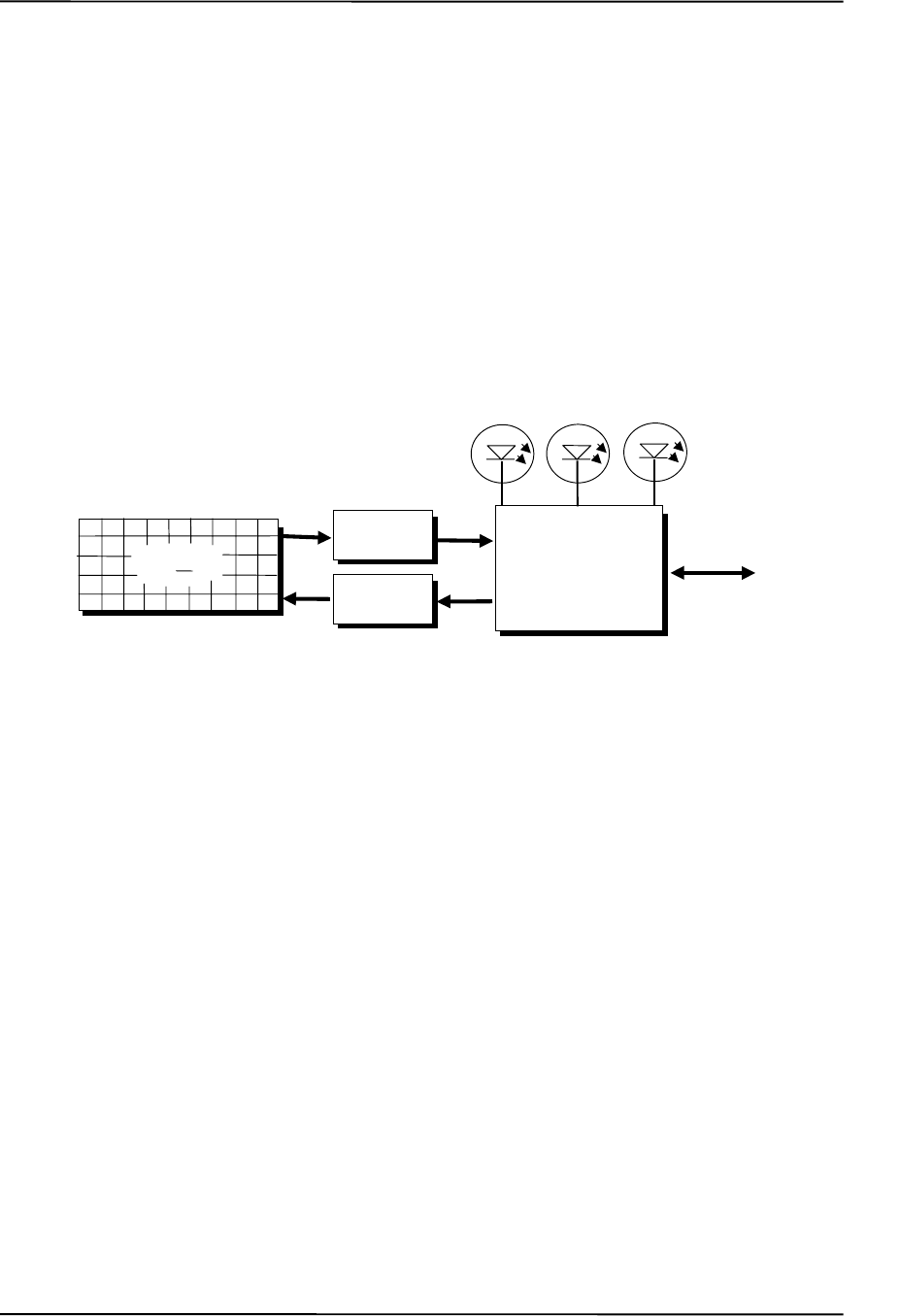
Appendix C Keyboard
Compaq Personal Computers
Changed - July 2000
C-2
C.2 KEYSTROKE PROCESSING
A functional block diagram of the keystroke processing elements is shown in Figure C-1. Power
(+5 VDC) is obtained from the system through the PS/2-type interface. The keyboard uses a
Z86C14 (or equivalent) microprocessor. The Z86C14 scans the key matrix drivers every 10 ms for
pressed keys while at the same time monitoring communications with the keyboard interface of the
system unit. When a key is pressed, a Make code is generated. A Break code is generated when the
key is released. The Make and Break codes are collectively referred to as scan codes. All keys
generate Make and Break codes with the exception of the Pause key, which generates a Make code
only.
Figure C–1. Keystroke Processing Elements, Block Diagram
When the system is turned on, the keyboard processor generates a Power-On Reset (POR) signal
after a period of 150 ms to 2 seconds. The keyboard undergoes a Basic Assurance Test (BAT) that
checks for shorted keys and basic operation of the keyboard processor. The BAT takes from 300 to
500 ms to complete.
If the keyboard fails the BAT, an error code is sent to the CPU and the keyboard is disabled until
an input command is received. After successful completion of the POR and BAT, a completion
code (AAh) is sent to the CPU and the scanning process begins.
The keyboard processor includes a 16-byte FIFO buffer for holding scan codes until the system is
ready to receive them. Response and typematic codes are not buffered. If the buffer is full (16
bytes held) a 17th byte of a successive scan code results in an overrun condition and the overrun
code replaces the scan code byte and any additional scan code data (and the respective key strokes)
are lost. Multi-byte sequences must fit entirely into the buffer before the respective keystroke can
be registered.
Keyboard
Interface
(System Unit)
Data/
CLK
Num
Lock Caps
Lock
Scroll
Lock
Keyboard
Processor
Matrix
Drivers
Matrix
Receivers
Keyswitch
Matrix
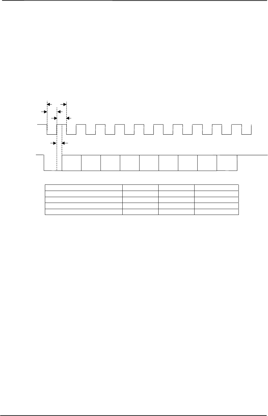
Technical Reference Guide
Compaq Personal Computers
Changed –- July 2000
C-3
C.2.1 PS/2-TYPE KEYBOARD TRANSMISSIONS
The PS/2-type keyboard sends two main types of data to the system; commands (or responses to
system commands) and keystroke scan codes. Before the keyboard sends data to the system
(specifically, to the 8042-type logic within the system), the keyboard verifies the clock and data
lines to the system. If the clock signal is low (0), the keyboard recognizes the inhibited state and
loads the data into a buffer. Once the inhibited state is removed, the data is sent to the system.
Keyboard-to-system transfers (in the default mode) consist of 11 bits as shown in Figure C-2.
Parameter Minimum Nominal Maximum
Tcy (clock cycle) 60 us -- 80 us
Tcl (clock low) 30 us 41 us 50 us
Tch (clock high) 30 us -- 40 us
Th-b-t (high-before-transmit) -- 20 us --
Figure C–2. PS/2 Keyboard-To-System Transmission, Timing Diagram
The system can halt keyboard transmission by setting the clock signal low. The keyboard checks
the clock line every 60 us to verify the state of the signal. If a low is detected, the keyboard will
finish the current transmission if the rising edge of the clock pulse for the parity bit has not
occurred. The system uses the same timing relationships during reads (typically with slightly
reduced time periods).
The enhanced keyboard has three operating modes:
♦ Mode 1 - PC-XT compatible
♦ Mode 2 - PC-AT compatible (default)
♦ Mode 3 - Select mode (keys are programmable as to make-only, break-only, typematic)
Modes can be selected by the user or set by the system. Mode 2 is the default mode. Each mode
produces a different set of scan codes. When a key is pressed, the keyboard processor sends that
key’s make code to the 8042 logic of the system unit. The When the key is released, a release code
is transmitted as well (except for the Pause key, which produces only a make code). The 8042-
type logic of the system unit responds to scan code reception by asserting IRQ1, which is
processed by the interrupt logic and serviced by the CPU with an interrupt service routine. The
service routine takes the appropriate action based on which key was pressed.
Tcy
Th-b-t
Clock
Tcl
Tch
Data
(LSb) (MSb)
Parity
Bit
Dat
a
Start
Bit Dat
aDat
aDat
aDat
aDat
aDat
aDat
aStop
Bit

Appendix C Keyboard
Compaq Personal Computers
Changed - July 2000
C-4
C.2.2 USB-TYPE KEYBOARD TRANSMISSIONS
The USB-type keyboard sends essentially the same information to the system that the PS/2
keyboard does except that the data receives additional NRZI encoding and formatting (prior to
leaving the keyboard) to comply with the USB I/F specification (discussed in chapter 5 of this
guide).
Packets received at the system’s USB I/F and decoded as originating from the keyboard result in
an SMI being generated. An SMI handler routine is invoked that decodes the data and transfers the
information to the 8042 keyboard controller where normal (legacy) keyboard processing takes
place.
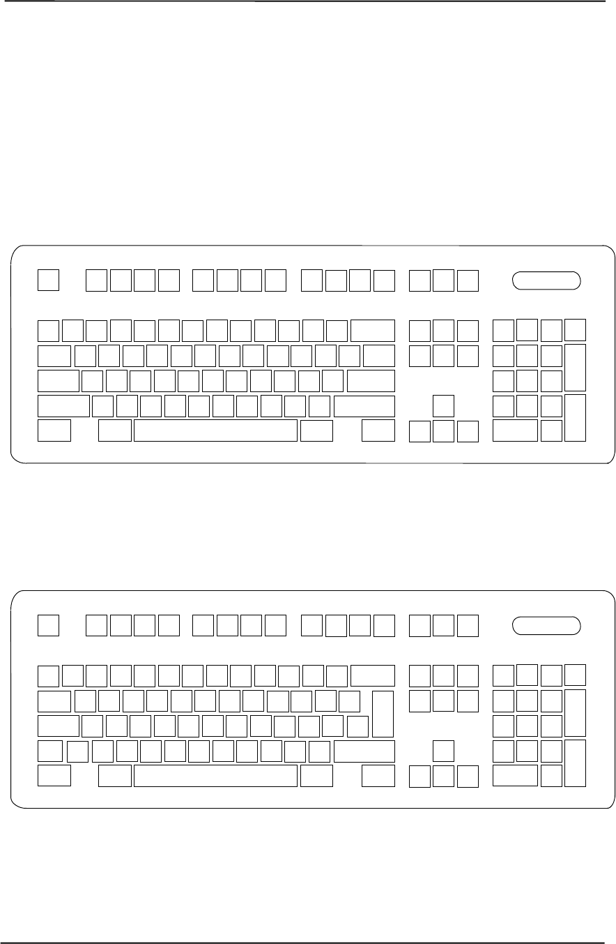
Technical Reference Guide
Compaq Personal Computers
Changed –- July 2000
C-5
C.2.3 KEYBOARD LAYOUTS
Figures C-3 through C-8 show the key layouts for keyboards shipped with Compaq systems. Actual
styling details including location of the Compaq logo as well as the numbers lock, caps lock, and
scroll lock LEDs may vary.
C.2.3.1 Standard Enhanced Keyboards
Figure C–3. U.S. English (101-Key) Keyboard Key Positions
Figure C–4. National (102-Key) Keyboard Key Positions
12345678910 11 12 13 14 15 16
17 18 19 20 21 22 23 24 25 26 27 28 29 31
39
32 33 34 35 36 37 38
40 41 42 43 44 45 46 47 48 30
49 50 51
59 60 61 62 63 64 65 66 67 68 69 70 71
75 76 77 78 79 80 81 82 83 84 85 86
92 93 94 95 96
52 53 54 55 56 57
72 73 74
88 89 90
100
58
91
87
97 98 99 101
12 3 4 5 67 8 9 10 11 12 13 14 15 16
17 18 19 20 21 22 23 24 25 26 27 28 29 31
39
32 33 34 35 36 37 38
40 41 42 43 44 45 46 47 48 49 50 51
59 60 61 62 63 64 65 66 67 68 69 70
75 76 77 78 79 80 81 82 83 84 85 86
92 93 94 95 96
52 53 54 55 56 57
72 73 74
88 89 90
100
58
91
87
97 98 99 101
104
71
103
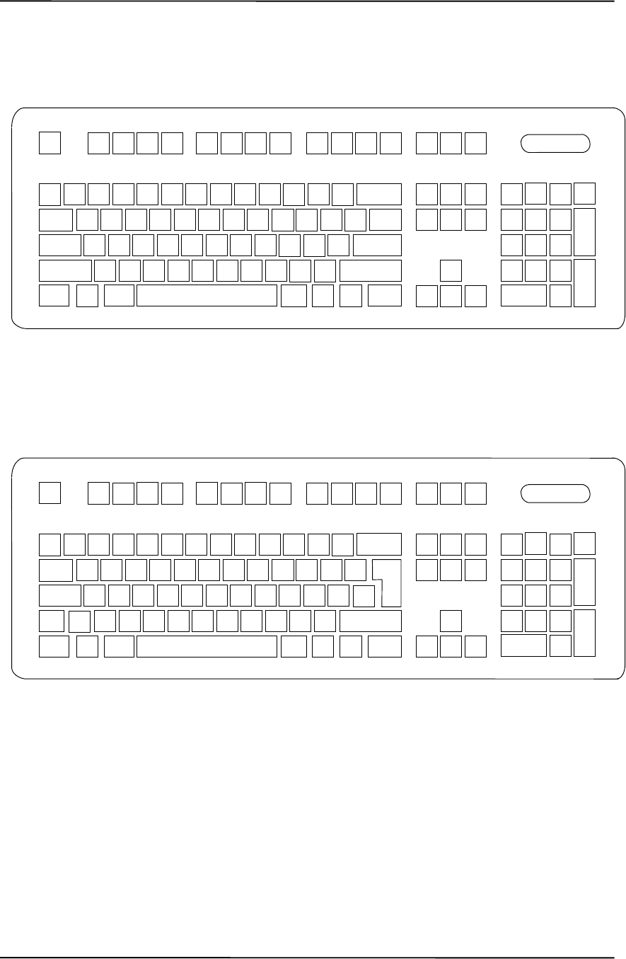
Appendix C Keyboard
Compaq Personal Computers
Changed - July 2000
C-6
C.2.3.2 Windows Enhanced Keyboards
Figure C–5. U.S. English Windows (101W-Key) Keyboard Key Positions
Figure C–6. National Windows (102W-Key) Keyboard Key Positions
12345678910 11 12 13 14 15 16
17 18 19 20 21 22 23 24 25 26 27 28 29 31
39
32 33 34 35 36 37 38
40 41 42 43 44 45 46 47 48 30
49 50 51
59 60 61 62 63 64 65 66 67 68 69 70 71
75 76 77 78 79 80 81 82 83 84 85 86
92 93 94 95 96
52 53 54 55 56 57
72 73 74
88 89 90
100
58
91
87
97 98 99 101110 111 112
12345678910 11 12 13 14 15 16
17 18 19 20 21 22 23 24 25 26 27 28 29 31
39
32 33 34 35 36 37 38
40 41 42 43 44 45 46 47 48 49 50 51
59 60 61 62 63 64 65 66 67 68 69 70
75 76 77 78 79 80 81 82 83 84 85 86
52 53 54 55 56 57
72 73 74
88 89 90
100
58
91
87
97 98 99 101
104
103
92 93 94 95 96
110 111 112
71
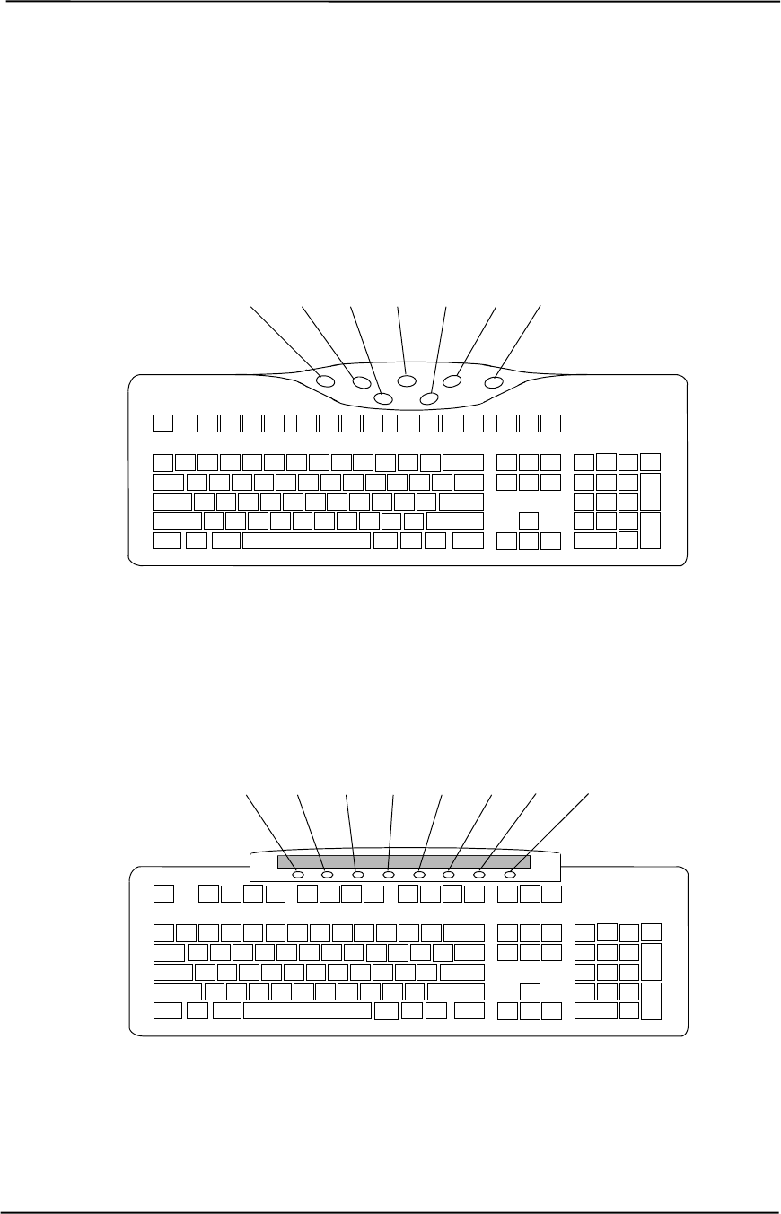
Technical Reference Guide
Compaq Personal Computers
Changed –- July 2000
C-7
C.2.3.3 Easy Access Keyboards
The Easy Access keyboard is a Windows Enhanced-type keyboard that includes special buttons
allowing quick internet navigation. Depending on system, either a 7-button or an 8-button layout
may be supplied.
The 7-button Easy Access Keyboard uses the layout shown in Figure C-7 and is available with
either a legacy PS/2-type connection or a Universal Serial Bus (USB) type connection.
NOTE: Main key positions same as Windows Enhanced (Figures C-5 or C-6).
Figure C–7. 7-Button Easy Access Keyboard Layout
The 8-button Easy Access Keyboard uses the layout shown in Figure C-8 and uses the PS/2-type
connection.
NOTE: Main key positions same as Windows Enhanced (Figures C-5 or C-6).
Figure C–8. 8-Button Easy Access Keyboard Layout
Btn 1 Btn 2 Btn 3 Btn 4 Btn 5 Btn 6 Btn 7
Btn 1 Btn 2 Btn 3 Btn 4 Btn 5 Btn 6 Btn 7 Btn 8

Appendix C Keyboard
Compaq Personal Computers
Changed - July 2000
C-8
C.2.4 KEYS
All keys generate a make code (when pressed) and a break code (when released) with the
exception of the Pause key (pos. 16), which produces a make code only. All keys with the
exception of the Pause and Easy Access keys are also typematic, although the typematic action of
the Shift, Ctrl, Alt, Num Lock, Scroll Lock, Caps Lock, and Ins keys is suppressed by the
BIOS. Typematic keys, when held down longer than 500 ms, send the make code repetitively at a
10-12 Hz rate until the key is released. If more than one key is held down, the last key pressed will
be typematic.
C.2.4.1 Special Single-Keystroke Functions
The following keys provide the intended function in most applications and environments.
Caps Lock - The Caps Lock key (pos. 59), when pressed and released, invokes a BIOS
routine that turns on the caps lock LED and shifts into upper case key positions 40-49, 60-68,
and 76-82. When pressed and released again, these keys revert to the lower case state and the
LED is turned off. Use of the Shift key will reverse which state these keys are in based on the
Caps Lock key.
Num Lock - The Num Lock key (pos. 32), when pressed and released, invokes a BIOS routine
that turns on the num lock LED and shifts into upper case key positions 55-57, 72-74, 88-90,
100, and 101. When pressed and released again, these keys revert to the lower case state and the
LED is turned off.
The following keys provide special functions that require specific support by the application.
Print Scrn - The Print Scrn (pos. 14) key can, when pressed, generate an interrupt that initiates
a print routine. This function may be inhibited by the application.
Scroll Lock - The Scroll Lock key (pos. 15) when pressed and released, , invokes a BIOS
routine that turns on the scroll lock LED and inhibits movement of the cursor. When pressed and
released again, the LED is turned off and the function is removed. This keystroke is always
serviced by the BIOS (as indicated by the LED) but may be inhibited or ignored by the
application.
Pause - The Pause (pos. 16) key, when pressed, can be used to cause the keyboard interrupt to
loop, i.e., wait for another key to be pressed. This can be used to momentarily suspend an
operation. The key that is pressed to resume operation is discarded. This function may be ignored
by the application.
The Esc, Fn (function), Insert, Home, Page Up/Down, Delete, and End keys operate at the
discretion of the application software.

Technical Reference Guide
Compaq Personal Computers
Changed –- July 2000
C-9
C.2.4.2 Multi-Keystroke Functions
Shift - The Shift key (pos. 75/86), when held down, produces a shift state (upper case) for keys in
positions 17-29, 30, 39-51, 60-70, and 76-85 as long as the Caps Lock key (pos. 59) is toggled
off. If the Caps Lock key is toggled on, then a held Shift key produces the lower (normal) case
for the identified pressed keys. The Shift key also reverses the Num Lock state of key positions
55-57, 72, 74, 88-90, 100, and 101.
Ctrl - The Ctrl keys (pos. 92/96) can be used in conjunction with keys in positions 1-13, 16, 17-
34, 39-54, 60-71, and 76-84. The application determines the actual function. Both Ctrl key
positions provide identical functionality. The pressed combination of Ctrl and Break (pos. 16)
results in the generation of BIOS function INT 1Bh. This software interrupt provides a method of
exiting an application and generally halts execution of the current program.
Alt - The Alt keys (pos. 93/95) can be used in conjunction with the same keys available for use
with the Ctrl keys with the exception that position 14 (SysRq) is available instead of position 16
(Break). The Alt key can also be used in conjunction with the numeric keypad keys (pos. 55-57,
72-74, and 88-90) to enter the decimal value of an ASCII character code from 1-255. The
application determines the actual function of the keystrokes. Both Alt key positions provide
identical functionality. The combination keystroke of Alt and SysRq results in software interrupt
15h, AX=8500h being executed. It is up to the application to use or not use this BIOS function.
The Ctrl and Alt keys can be used together in conjunction with keys in positions 1-13, 17-34, 39-
54, 60-71, and 76-84. The Ctrl and Alt key positions used and the sequence in which they are
pressed make no difference as long as they are held down at the time the third key is pressed. The
Ctrl, Alt, and Delete keystroke combination (required twice if in the Windows environment)
initiates a system reset (warm boot) that is handled by the BIOS.
C.2.4.3 Windows Keystrokes
Windows-enhanced keyboards include three additional key positions. Key positions 110 and 111
(marked with the Windows logo ) have the same functionality and are used by themselves or
in combination with other keys to perform specific “hot-key” type functions for the Windows
operating system. The defined functions of the Windows logo keys are listed as follows:
Keystroke Function
Window Logo Open Start menu
Window Logo + F1 Display pop-up menu for the selected object
Window Logo + TAB Activate next task bar button
Window Logo + E Explore my computer
Window Logo + F Find document
Window Logo + CTRL + F Find computer
Window Logo + M Minimize all
Shift + Window Logo + M Undo minimize all
Window Logo + R Display Run dialog box
Window Logo + PAUSE Perform system function
Window Logo + 0-9 Reserved for OEM use (see following text)
The combination keystroke of the Window Logo + 1-0 keys are reserved for OEM use for
auxiliary functions (speaker volume, monitor brightness, password, etc.).
Key position 112 (marked with an application window icon ) is used in combination with other
keys for invoking Windows application functions.
Appendix C Keyboard
Compaq Personal Computers
Changed - July 2000
C-10
C.2.4.4 Easy Access Keystrokes
The Easy Access keyboards (Figures C-7 and C-8) include additional keys (also referred to as
buttons) used to streamline internet access and navigation.
These buttons, which can be re-programmed to provide other functions, have the default
functionality described below:
7-Button Easy Access Keyboard:
Button # Description Default Function
1 Check email Email
2 Go to community Emoney
3 Extra web site Compaq web site
4 Go to favorite web site AltaVista web site
5 Internet search Search
6 Instant answer Travel expenses
7 E-commerce Shopping
8-Button Easy Access Keyboard:
Button # Description Default Function
1 Go to favorite web site Customer web site of choice
2 Go to AltaVista AltaVista web site
3 Search AltaVista search engine
4 Check Email Launches user Email
5 Business Community Industry specification info
6 Market Monitor Launches Bloomberg market monitor
7 Meeting Center Links to user’s project center
8 News/PC Lock News retrieval service
All buttons may be re-programmed by the user through the Easy Access utility.

Technical Reference Guide
Compaq Personal Computers
Changed –- July 2000
C-11
C.2.5 KEYBOARD COMMANDS
Table C-1 lists the commands that the keyboard can send to the system (specifically, to the 8042-
type logic).
Table C–1. Keyboard-to-System Commands
Table C-1.
Keyboard-to-System Commands
Command Value Description
Key Detection Error/Over/run 00h [1]
FFh [2] Indicates to the system that a switch closure couldn’t be
identified.
BAT Completion AAh Indicates to the system that the BAT has been successful.
BAT Failure FCh Indicates failure of the BAT by the keyboard.
Echo EEh Indicates that the Echo command was received by the
keyboard.
Acknowledge (ACK) FAh Issued by the keyboard as a response to valid system
inputs (except the Echo and Resend commands).
Resend FEh Issued by the keyboard following an invalid input.
Keyboard ID 83ABh Upon receipt of the Read ID command from the system,
the keyboard issues the ACK command followed by the
two IDS bytes.
Note: [1] Modes 2 and 3.
[2] Mode 1 only.
C.2.6 SCAN CODES
The scan codes generated by the keyboard processor are determined by the mode the keyboard is
operating in.
♦ Mode 1: In Mode 1 operation, the keyboard generates scan codes compatible with 8088-
/8086-based systems. To enter Mode 1, the scan code translation function of the keyboard
controller must be disabled. Since translation is not performed, the scan codes generated in
Mode 1 are identical to the codes required by BIOS. Mode 1 is initiated by sending command
F0h with the 01h option byte. Applications can obtain system codes and status information by
using BIOS function INT 16h with AH=00h, 01h, and 02h.
♦ Mode 2: Mode 2 is the default mode for keyboard operation. In this mode, the 8042 logic
translates the make codes from the keyboard processor into the codes required by the BIOS.
This mode was made necessary with the development of the Enhanced III keyboard, which
includes additional functions over earlier standard keyboards. Applications should use BIOS
function INT 16h, with AH=10h, 11h, and 12h for obtaining codes and status data. In Mode 2,
the keyboard generates the Break code, a two-byte sequence that consists of a Make code
immediately preceded by F0h (i.e., Break code for 0Eh is “F0h 0Eh”).
♦ Mode 3: Mode 3 generates a different scan code set from Modes 1 and 2. Code
translation must be disabled since translation for this mode cannot be done.

Appendix C Keyboard
Compaq Personal Computers
Changed - July 2000
C-12
Table C–2. Keyboard Scan Codes
Table C-2.
Keyboard Scan Codes
Key
Pos. Legend Mode 1 Mode 2 Mode 3
1 Esc 01/81 76/F0 76 08/na
2 F1 3B/BB 05/F0 05 07/na
3 F2 3C/BC 06/F0 06 0F/na
4 F3 3D/BD 04/F0 04 17/na
5 F4 3E/BE 0C/F0 0C 1F/na
6 F5 3F/BF 03/F0 03 27/na
7 F6 40/C0 0B/F0 0B 2F/na
8 F7 41/C1 83/F0 83 37/na
9 F8 42/C2 0A/F0 0A 3F/na
10 F9 43/C3 01/FO 01 47/na
11 F10 44/C4 09/F0 09 4F/na
12 F11 57/D7 78/F0 78 56/na
13 F12 58/D8 07/F0 07 5E/na
14 Print Scrn E0 2A E0 37/E0 B7 E0 AA
E0 37/E0 B7 [1] [2]
54/84 [3]
E0 2A E0 7C/E0 F0 7C E0 F0 12
E0 7C/E0 F0 7C [1] [2]
84/F0 84 [3]
57/na
15 Scroll Lock 46/C6 7E/F0 7E 5F/na
16 Pause E1 1D 45 E1 9D C5/na
E0 46 E0 C6/na [3] E1 14 77 E1 F0 14 F0 77/na
E0 7E E0 F0 7E/na [3] 62/na
17 ` 29/A9 0E/F0 E0 0E/F0 0E
18 1 02/82 16/F0 16 46/F0 46
19 2 03/83 1E/F0 1E 1E/F0 1E
20 3 04/84 26/F0 26 26/F0 26
21 4 05/85 25/F0 25 25/F0 25
22 5 06/86 2E/F0 2E 2E/F0 2E
23 6 07/87 36/F0 36 36/F0 36
24 7 08/88 3D/F0 3D 3D/F0 3D
25 8 09/89 3E/F0 3E 3E/F0 3E
26 9 0A/8A 46/F0 46 46/F0 46
27 0 0B/8B 45/F0 45 45/F0 45
28 - 0C/8C 4E/F0 4E 4E/F0 4E
29 = 0D/8D 55/F0 55 55/F0 55
30 \ 2B/AB 5D/F0 5D 5C/F0 5C
31 Backspace 0E/8E 66/F0 66 66/F0 66
32 Insert E0 52/E0 D2
E0 AA E0 52/E0 D2 E0 2A [4]
E0 2A E0 52/E0 D2 E0 AA [6]
E0 70/E0 F0 70
E0 F0 12 E0 70/E0 F0 70 E0 12 [5]
E0 12 E0 70/E0 F0 70 E0 F0 12 [6]
67/na
33 Home E0 47/E0 D2
E0 AA E0 52/E0 D2 E0 2A [4]
E0 2A E0 47/E0 C7 E0 AA [6]
E0 6C/E0 F0 6C
E0 F0 12 E0 6C/E0 F0 6C E0 12 [5]
E0 12 E0 6C/E0 F0 6C E0 F0 12 [6]
6E/na
34 Page Up E0 49/E0 C7
E0 AA E0 49/E0 C9 E0 2A [4]
E0 2A E0 49/E0 C9 E0 AA [6]
E0 7D/E0 F0 7D
E0 F0 12 E0 7D/E0 F0 7D E0 12 [5]
E0 12 E0 7D/E0 F0 7D E0 F0 12 [6]
6F/na
35 Num Lock 45/C5 77/F0 77 76/na
36 / E0 35/E0 B5
E0 AA E0 35/E0 B5 E0 2A [1] E0 4A/E0 F0 4A
E0 F0 12 E0 4A/E0 F0 4A E0 12 [1] 77/na
37 * 37/B7 7C/F0 7C 7E/na
38 - 4A/CA 7B/F0 7B 84/na
39 Tab 0F/8F 0D/F0 0D 0D/na
40 Q 10/90 15/F0 15 15/na
Continued
([x] Notes listed at end of table.)
Make / Break Codes (Hex)

Technical Reference Guide
Compaq Personal Computers
Changed –- July 2000
C-13
Table C-2. Keyboard Scan Codes (Continued)
Key
Pos Legend Mode 1 Mode 2 Mode 3
41 W 11/91 1D/F0 1D 1D/F0 1D
42 E 12/92 24/F0 24 24/F0 24
43 R 13/93 2D/F0 2D 2D/F0 2D
44 T 14/94 2C/F0 2C 2C/F0 2C
45 Y 15/95 35/F0 35 35/F0 35
46 U 16/96 3C/F0 3C 3C/F0 3C
47 I 17/97 43/F0 43 43/F0 43
48 O 18/98 44/F0 44 44/F0 44
49 P 19/99 4D/F0 4D 4D/F0 4D
50 [ 1A/9A 54/F0 54 54/F0 54
51 ] 1B/9B 5B/F0 5B 5B/F0 5B
52 Delete E0 53/E0 D3
E0 AA E0 53/E0 D3 E0 2A [4]
E0 2A E0 53/E0 D3 E0 AA [6]
E0 71/E0 F0 71
E0 F0 12 E0 71/E0 F0 71 E0 12
[5]
E0 12 E0 71/E0 F0 71 E0 F0 12
[6]
64/F0 64
53 End E0 4F/E0 CF
E0 AA E0 4F/E0 CF E0 2A [4]
E0 2A E0 4F/E0 CF E0 AA [6]
E0 69/E0 F0 69
E0 F0 12 E0 69/E0 F0 69 E0 12
[5]
E0 12 E0 69/E0 F0 69 E0 F0 12
[6]
65/F0 65
54 Page Down E0 51/E0 D1
E0 AA E0 51/E0 D1 E0 2A [4]
E0 @a E0 51/E0 D1 E0 AA [6]
E0 7A/E0 F0 7A
E0 F0 12 E0 7A/E0 F0 7A E0 12
[5]
E0 12 E0 7A/E0 F0 7A E0 F0 12
[6]
6D/F0 6D
55 7 47/C7 [6] 6C/F0 6C [6] 6C/na [6]
56 8 48/C8 [6] 75/F0 75 [6] 75/na [6]
57 9 49/C9 [6] 7D/F0 7D [6] 7D/na [6]
58 + 4E/CE [6] 79/F0 79 [6] 7C/F0 7C
59 Caps Lock 3A/BA 58/F0 58 14/F0 14
60 A 1E/9E 1C/F0 1C 1C/F0 1C
61 S 1F/9F 1B/F0 1B 1B/F0 1B
62 D 20/A0 23/F0 23 23/F0 23
63 F 21/A1 2B/F0 2B 2B/F0 2B
64 G 22/A2 34/F0 34 34/F0 34
65 H 23/A3 33/F0 33 33/F0 33
66 J 24/A4 3B/F0 3B 3B/F0 3B
67 K 25/A5 42/F0 42 42/F0 42
68 L 26/A6 4B/F0 4B 4B/F0 4B
69 ; 27/A7 4C/F0 4C 4C/F0 4C
70 ‘ 28/A8 52/F0 52 52/F0 52
71 Enter 1C/9C 5A/F0 5A 5A/F0 5A
72 4 4B/CB [6] 6B/F0 6B [6] 6B/na [6]
73 5 4C/CC [6] 73/F0 73 [6] 73/na [6]
74 6 4D/CD [6] 74/F0 74 [6] 74/na [6]
75 Shift (left) 2A/AA 12/F0 12 12/F0 12
76 Z 2C/AC 1A/F0 1A 1A/F0 1A
77 X 2D/AD 22/F0 22 22/F0 22
78 C 2E/AE 21/F0 21 21/F0 21
79 V 2F/AF 2A/F0 2A 2A/F0 2A
80 B 30/B0 32/F0 32 32/F0 32
Continued
([x] Notes listed at end of table.)
Make / Break Codes (Hex)

Appendix C Keyboard
Compaq Personal Computers
Changed - July 2000
C-14
Table C-2. Keyboard Scan Codes (Continued)
Key
Pos. Legend Mode 1 Mode 2 Mode 3
81 N 31/B1 31/F0 31 31/F0 31
82 M 32/B2 3A/F0 3A 3A/F0 3A
83 , 33/B3 41/F0 41 41/F0 41
84 . 34/B4 49/F0 49 49/F0 49
85 / 35/B5 4A/F0 4A 4A/F0 4A
86 Shift (right) 36/B6 59/F0 59 59/F0 59
87 E0 48/E0 C8
E0 AA E0 48/E0 C8 E0 2A [4]
E0 2A E0 48/E0 C8 E0 AA [6]
E0 75/E0 F0 75
E0 F0 12 E0 75/E0 F0 75 E0 12 [5]
E0 12 E0 75/E0 F0 75 E0 F0 12 [6]
63/F0 63
88 1 4F/CF [6] 69/F0 69 [6] 69/na [6]
89 2 50/D0 [6] 72/F0 72 [6] 72/na [6]
90 3 51/D1 [6] 7A/F0 7A [6] 7A/na [6]
91 Enter E0 1C/E0 9C E0 5A/F0 E0 5A 79/F0
79[6]
92 Ctrl (left) 1D/9D 14/F0 14 11/F0 11
93 Alt (left) 38/B8 11/F0 11 19/F0 19
94 (Space) 39/B9 29/F0 29 29/F0 29
95 Alt (right) E0 38/E0 B8 E0 11/F0 E0 11 39/na
96 Ctrl (right) E0 1D/E0 9D E0 14/F0 E0 14 58/na
97 E0 4B/E0 CB
E0 AA E0 4B/E0 CB E0 2A [4]
E0 2A E0 4B/E0 CB E0 AA [6]
E0 6B/Eo F0 6B
E0 F0 12 E0 6B/E0 F0 6B E0 12[5]
E0 12 E0 6B/E0 F0 6B E0 F0 12[6]
61/F0 61
98 E0 50/E0 D0
E0 AA E0 50/E0 D0 E0 2A [4]
E0 2A E0 50/E0 D0 E0 AA [6]
E0 72/E0 F0 72
E0 F0 12 E0 72/E0 F0 72 E0 12[5]
E0 12 E0 72/E0 F0 72 E0 F0 12[6]
60/F0 60
99 E0 4D/E0 CD
E0 AA E0 4D/E0 CD E0 2A [4]
E0 2A E0 4D/E0 CD E0 AA [6]
E0 74/E0 F0 74
E0 F0 12 E0 74/E0 F0 74 E0 12[5]
E0 12 E0 74/E0 F0 74 E0 F0 12[6]
6A/F0 6A
100 0 52/D2 [6] 70/F0 70 [6] 70/na [6]
101 . 53/D3 [6] 71/F0 71 [6] 71/na [6]
102 na 7E/FE 6D/F0 6D 7B/F0 7B
103 na 2B/AB 5D/F0 5D 53/F0 53
104 na 36/D6 61/F0 61 13/F0 13
110 (Win95)
[7] E0 5B/E0 DB
E0 AA E0 5B/E0 DB E0 2A [4]
E0 2A E0 5B/E0 DB E0 AA [6]
E0 1F/E0 F0 1F
E0 F0 12 E0 1F/E0 F0 1F E0 12 [5]
E0 12 E0 1F/E0 F0 1F E0 F0 12 [6]
8B/F0 8B
111 (Win95)
[7] E0 5C/E0 DC
E0 AA E0 5C/E0 DC E0 2A [4]
E0 2A E0 5C/E0 DC E0 AA [6]
E0 2F/E0 F0 27
E0 F0 12 E0 27/E0 F0 27 E0 12 [5]
E0 12 E0 27/E0 F0 27 E0 F0 12 [6]
8C/F0 8C
112 (Win
Apps)
[7]
E0 5D/E0 DD
E0 AA E0 5D/E0 DD E0 2A [4]
E0 2A E0 5D E0 DD E0 AA [6]
E0 2F/E0 F0 2F
E0 F0 12 E0 2F/E0 F0 2F E0 12 [5]
E0 12 E0 2F/E0 F0 2F E0 F0 12 [6
8D/F0 8D
Continued
([x] Notes listed at end of table.)
Make / Break Codes (Hex)

Technical Reference Guide
Compaq Personal Computers
Changed –- July 2000
C-15
Table C-2. Keyboard Scan Codes (Continued)
Key
Pos. Legend Mode 1 Mode 2 Mode 3
Btn 1 [8] E0 1E/E0 9E E0 1C/E0 F0 1C 95/F0 95
Btn 2 [8] E0 26/E0 A6 E0 4B/E0 F0 4B 9C/F0 9C
Btn 3 [8] E0 25/E0 A5 E0 42/E0 F0 42 9D/F0 9D
Btn 4 [8] E0 23/E0 A3 E0 33/E0 F0 33 9A/F0 9A
Btn 5 [8] E0 21/E0 A1 E0 2B/E0 F0 2B 99/F0 99
Btn 6 [8] E0 12/E0 92 E0 24/E0 F0 24 96/F0 96
Btn 7 [8] E0 32/E0 B2 E0 3A/E0 F0 3A 97/F0 97
Btn 1 [9] E0 23/E0 A3 E0 33/E0 F0 33 9A/F0 9A
Btn 2 [9] E0 1F/E0 9F E0 1B/E0 F0 1B 80/F0 80
Btn 3 [9] E0 1A/E0 9A E0 54/E0 F0 54 99/F0 99
Btn 4 [9] E0 1E/E0 9E E0 1C/E0 F0 1C 95/F0 95
Btn 5 [9] E0 13/E0 93 E0 2D/E0 F0 2D 0C/F0 0C
Btn 6 [9] E0 14/E0 94 E0 2C/E0 F0 2C 9D/F0 9D
Btn 7 [9] E0 15/E0 95 E0 35/E0 F0 35 96/F0 96
Btn 8 [9] E0 1B/E0 9B E0 5B/E0 F0 5B 97/F0 97
NOTES: All codes assume Shift, Ctrl, and Alt keys inactive unless otherwise noted.
NA = Not applicable
[1] Shift (left) key active.
[2] Ctrl key active.
[3] Alt key active.
[4] Left Shift key active. For active right Shift key, substitute AA/2A make/break codes for B6/36
codes. [5] Left Shift key active. For active right Shift key, substitute F0 12/12 make/break codes
for F0 59/59 codes.
[6] Num Lock key active.
[7] Windows keyboards only.
[8] 7-Button Easy Access keyboard.
[9] 8-Button Easy Access keyboard.
Make / Break Codes (Hex)
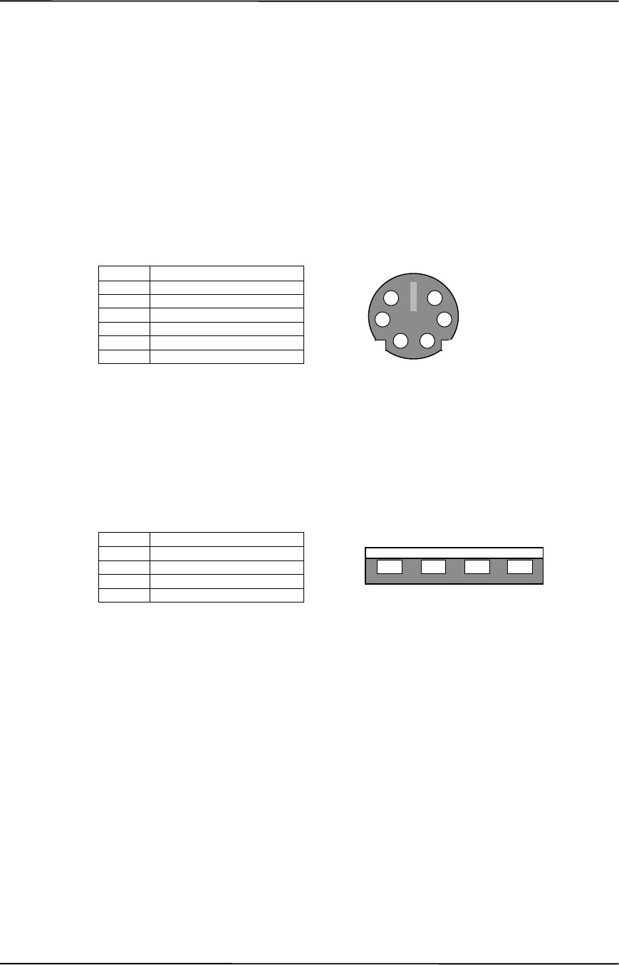
Appendix C Keyboard
Compaq Personal Computers
Changed - July 2000
C-16
C.3 CONNECTORS
Two types of keyboard interfaces are used in Compaq systems: PS/2-type and USB-type. System
units that provide a PS/2 connector will ship with a PS/2-type keyboard but may also support
simultaneous connection of a USB keyboard. Systems that do not provide a PS/2 interface will
ship with a USB keyboard. For a detailed description of the PS/2 and USB interfaces refer to
chapter 5 “Input/Output” of this guide. The keyboard cable connectors and their pinouts are
described in the following figures:
Pin Function
1Data
2 Not connected
3 Ground
4+5 VDC
5Clock
6 Not connected
Figure C–9. PS/2 Keyboard Cable Connector (Male)
Pin Function
1+5 VDC
2 Data (+)
3 Data (-)
4 Ground
Figure C–10. USB Keyboard Cable Connector (Male)
65
43
21
1234
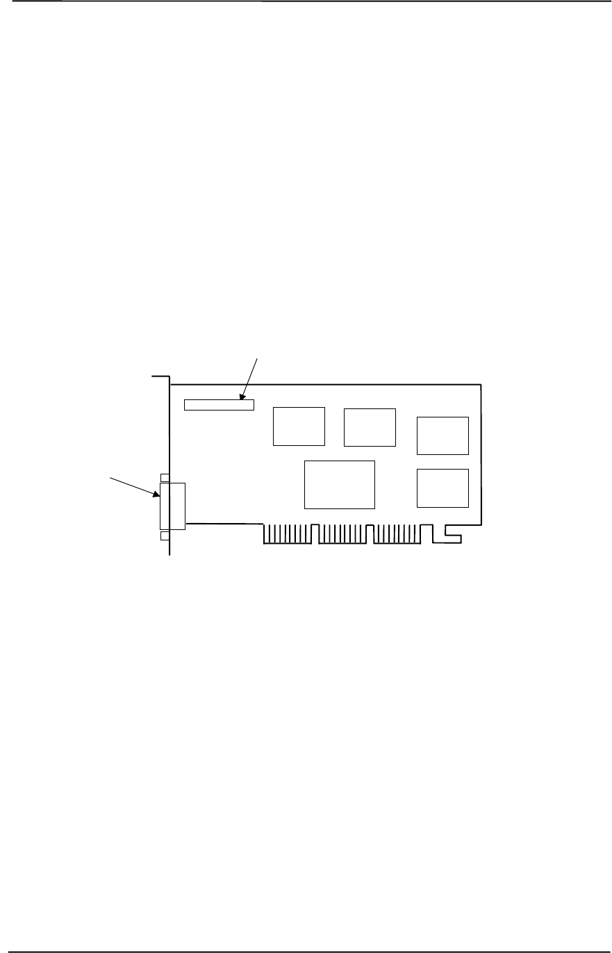
Technical Reference Guide
Compaq Personal Computers
Original - July 2000 D-1
Appendix D
COMPAQ/NVIDIA TNT2 PRO
AGP GRAPHICS CARD
D. Appendix D Compaq/NVIDIA TNT2 Pro AGP Graphics Card
D.1 INTRODUCTION
This appendix describes the Compaq/NVIDIA TNT2 Pro AGP Graphics Card used in the standard
configuration on some models and also available as an option. This card (layout shown in the
following figure) installs in a system’s AGP slot. The Compaq/NVIDIA TNT2 Pro graphics card
(P/N 189998-B21) provides high 2D performance as well as 3D capabilities.
Figure D-1. Compaq/NVIDIA TNT2 Pro AGP Graphics Card (P/N 198998-B21) Layout
This appendix covers the following subjects:
♦ Functional description (D.2) page D-2
♦ Display modes (D.3) page D-3
♦ Software support information (D.4) page D-4
♦ Monitor power management (D.5) page D-4
♦ Connectors (D.6) page D-5
Feature Connector
NVIDIA
TNT2
Controller SGRAM
SGRAM
SGRAM SGRAM
Analog
Monitor
Connector

Appendix D Compaq/NVIDIA TNT2 Pro AGP Graphics Card
Compaq Personal Computers
Original - July 2000
D-2
D.2 FUNCTIONAL DESCRIPTION
The NVIDIA TNT2 Pro-SD Graphics Card provides high performance 2D and 3D display
imaging. The card’s AGP design provides an economical approach to 3D processing by off-
loading 3D effects such as texturing, z-buffering and alpha blending to the system memory while
16 megabytes of on-board SGRAM stores the main display image.
Figure D-2. NVIDIA TNT2 Pro Graphics Card Block diagram
The NVIDIA TNT2 Pro Graphics Card includes the following features:
♦ 16-MB SGRAM frame buffer using 128-bit 166-MHz access
♦ AGP 4X transfers with sideband addressing
♦ 2D drawing engine
♦ 3D rendering engine
♦ 300-MHz RAMDAC
♦ 32-bit Z/stencil buffer eliminates hidden screen portions for faster loading
♦ 32-bit color for increased image quality
♦ 30-fps full-screen DVD playback
♦ Dual-monitor support with a PCI graphics card
BIOS
ROM
HSync
128-bit
166-MHz
Data Bus
Analog
Monitor
Connector
RGB
NVIDIA TNT2 Graphics Controller
3D Array
Engine
Video
Scalar
300-MHz
RAM
DAC
CRT
Controller
Memory
I/F
AGP
Bus
Card
Edge
Connector VSync
2D/VGA
Engine
16 MB
SGRAM
Frame Buffer
AGP 4X
I/F

Technical Reference Guide
Compaq Personal Computers
Original - July 2000 D-3
D.3 DISPLAY MODES
The graphics display modes supported by the NVIDIA TNT2 Pro Graphics are listed in Table D-1.
Table D-1. NVIDIA TNT2 Pro Graphics Display Modes
Table D-1.
NVIDIA TNT2 Pro Graphics Display Modes
Resolution Bits per pixel Color Depth Max. Refresh Frequency (Hz)
640 x 480 8 256 85
640 x 480 16 65K 85
640 x 480 24 16.7M 85
800 x 600 8 256 85
800 x 600 16 65K 85
800 x 600 24 16.7M 85
1024 x 768 8 256 85
1024 x 768 16 65K 85
1024 x 768 24 16.7M 85
1152 x 864 8 256 85
1152 x 864 16 65K 85
1152 x 864 24 16.7M 85
1280 x 1024 8 256 85
1280 x 1024 16 65K 85
1280 x 1024 24 16.7M 85
1600 x 1200 8 256 85
1600 x 1200 16 65K 85
1600 x 1200 24 16.7M 85
1800 x 1440 8 256 85
1800 x 1440 16 65K 85
1800 x 1440 24 16.7M 85
1920 x 1080 8 256 85
1920 x 1080 16 65K 85
1920 x 1080 24 16.7M 85
1920 x 1200 8 256 75

Appendix D Compaq/NVIDIA TNT2 Pro AGP Graphics Card
Compaq Personal Computers
Original - July 2000
D-4
D.4 SOFTWARE SUPPORT INFORMATION
The NVIDIA TNT2 Pro graphics card is fully compatible with software written for legacy video
modes (VGA, EGA, CGA) and needs no driver support for those modes.
Drivers are provided with or available for the card to provide extended mode support for the
current operating systems and programming environments such as:
♦ Windows 98, 95
♦ Windows NT 4.0, 3.51
♦ Windows 3.11, 3.1
♦ OS/2
♦ Quick Draw
♦ MS Direct Draw and Direct X
♦ Direct 3D
♦ OpenGL
D.5 POWER MANAGEMENT AND CONSUMPTION
This controller provides monitor power control for monitors that conform to the VESA display
power management signaling (DPMS) protocol. This protocol defines different power
consumption conditions and uses the HSYNC and VSYNC signals to select a monitor’s power
condition. Table I-2 lists the monitor power conditions.
Table D-2. Monitor Power Management Conditions
Table D-2.
Monitor Power Management Conditions
HSYNC VSYNC Power Mode Description
Active Active On Monitor is completely powered up. If activated, the inactivity
counter counts down during system inactivity and if allowed to
tiemout, generates an SMI to initiate the Suspend mode.
Active Inactive Suspend Monitor’s high voltage section is turned off and CRT heater
(filament) voltage is reduced from 6.6 to 4.4 VDC. The Off mode
inactivity timer counts down from the preset value and if allowed
to timeout, another SMI is generated and serviced, resulting in
the monitor being placed into the Off mode. Wake up from
Suspend mode is typically a few seconds.
Inactive Inactive Off Monitor’s high voltage section and heater circuitry is turned off.
Wake up from Off mode is a little longer than from Suspend.
The graphics card’s maximum power consumption on the AGP bus is listed below:
Maximum current draw @ 3.3 VDC: 3.0 A
Maximum current draw @ 5.0 VDC: 50 mA
Maximum current draw @ 1.5 VDC: 10 mA
Maximum power consumption: 10.2 watts
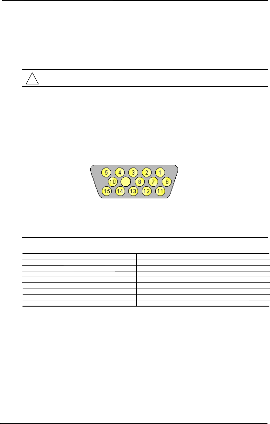
Technical Reference Guide
Compaq Personal Computers
Original - July 2000 D-5
D.6 CONNECTORS
There are two connectors associated with the graphics subsystem; the display/monitor connector
and the Feature connector.
NOTE: The graphic card’s edge connector mates with the AGP slot connector on the
system board. This interface is described in chapter 4 of this guide.
The DB-15 disply/monitor connector is provided for connection of a compatible RGB/analog
monitor. The Feature connector allows the attachment of an optional card such as a video tuner.
D.6.1 MONITOR CONNECTOR
Figure D-3. VGA Monitor Connector, (Female DB-15, as viewed from rear).
Table D-3. DB-15 Monitor Connector Pinout
Table D-3.
DB-15 Monitor Connector Pinout
Pin Signal Description Pin Signal Description
1 R Red Analog 9 PWR +5 VDC (fused) [1]
2 G Blue Analog 10 GND Ground
3 B Green Analog 11 NC Not Connected
4 NC Not Connected 12 SDA DDC2-B Data
5 GND Ground 13 HSync Horizontal Sync
6 R GND Red Analog Ground 14 VSync Vertical Sync
7 G GND Green Analog Ground 15 SCL DDC2-B Clock
8 B GND Blue Analog Ground -- -- --
NOTES: [1] Fuse automatically resets when excessive load is removed.
9

Appendix D Compaq/NVIDIA TNT2 Pro AGP Graphics Card
Compaq Personal Computers
Original - July 2000
D-6
This page is intentionally blank.
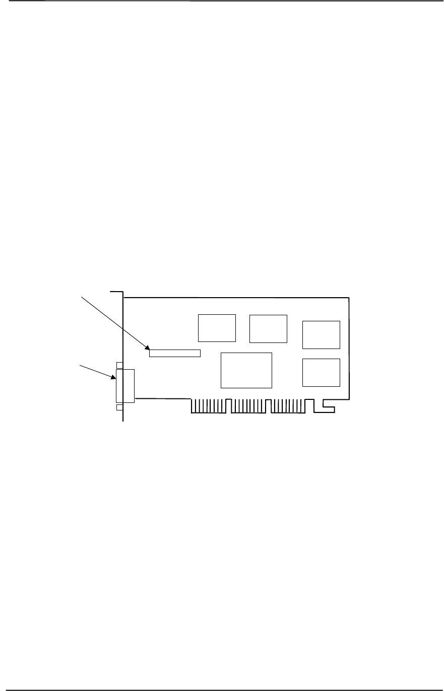
Technical Reference Guide
Compaq Personal Computers
Original - November 2000 E-1
Appendix E
COMPAQ/NVIDIA GeForce2 GTS
AGP GRAPHICS CARD
E. Appendix E Compaq/NVIDIA GeForce2 GTS AGP Graphics
Card
E.1 INTRODUCTION
This appendix describes the Compaq/NVIDIA GeForce2 GTS AGP Graphics Card used in the
standard configuration on some models and also available as an option. This card (layout shown in
the following figure) installs in a system’s AGP slot. The Compaq/NVIDIA GeForce2 GTS
graphics card (P/N 189998-B21) provides high 2D performance as well as 3D capabilities.
Figure E-1. Compaq/NVIDIA GeForce2 GTS AGP Graphics Card (P/N 179642-001) Layout
This appendix covers the following subjects:
♦ Functional description (D.2) page D-2
♦ Display modes (D.3) page D-3
♦ Software support information (D.4) page D-4
♦ Monitor power management (D.5) page D-4
♦ Connectors (D.6) page D-5
Feature Connector
NVIDIA
NV15
Controller SDRAM
SDRAM
SDRAM SDRAM
RGB Monitor
Connector
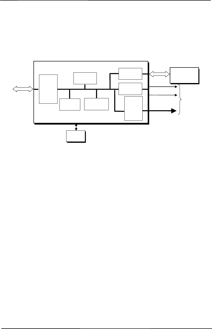
Appendix E Compaq/NVIDIA GeForce2 GTS AGP Graphics Card
Compaq Personal Computers
Original - November 2000
E-2
E.2 FUNCTIONAL DESCRIPTION
The NVIDIA GeForce2 GTS-SD Graphics Card provides high performance 2D and 3D display
imaging. The card’s AGP design provides an economical approach to 3D processing by off-
loading 3D effects such as texturing, z-buffering and alpha blending to the system memory while
32 megabytes of on-board SDRAM stores the main display image.
Figure E-2. NVIDIA GeForce2 GTS Graphics Card Block diagram
The NVIDIA GeForce2 GTS Graphics Card includes the following features:
♦ 16-MB SDRAM frame buffer using 128-bit 166-MHz access
♦ AGP 4X transfers with sideband addressing
♦ 2D drawing engine with:
• 128-bit BitBLTs, rectangle/polygon fills, line draws
• Hardware cursor
• 8-/16-/32-bpp mode acceleration
♦ 3D accelerator with:
• Hardware transform and lighting
• Single-pass dual textures
• 4 rendering pipelines
• Anistropic filtering
• 8-bit stencil buffer
• Specular lighting diffuse shading
• 16-/24-bit Z-buffering
♦ 350-MHz RAMDAC
♦ VESA compliancy:
• VIP 1.1 connector
• DDC2B monitor support
• DPMS, EPA Energy Star, and ACPI-compliant power management
BIOS
ROM
HSync
128-bit
166-MHz
Data Bus
Analog
Monitor
Connector
RGB
NVIDIA N15 Graphics Controller
3D Array
Engine
Video
Scalar
350-MHz
RAM
DAC
CRT
Controller
Memory
I/F
AGP
Bus
Card
Edge
Connector VSync
2D/VGA
Engine
32 MB
SDRAM
Frame Buffer
AGP 4X
I/F

Technical Reference Guide
Compaq Personal Computers
Original - November 2000 E-3
E.3 DISPLAY MODES
The graphics display modes supported by the NVIDIA GeForce2 GTS Graphics are listed in Table
E-1.
Table E-1. NVIDIA GeForce2 GTS Graphics Display Modes
Table E-1.
NVIDIA GeForce2 GTS Graphics Display Modes
Resolution Bits per pixel Color Depth Max. Refresh Frequency (Hz)
640 x 480 8 256 240
640 x 480 16 65K 240
640 x 480 32 16.7M 240
800 x 600 8 256 240
800 x 600 16 65K 240
800 x 600 32 16.7M 240
960 x 720 8 256 120
960 x 720 16 65K 120
960 x 720 32 16.7M 120
1024 x 768 8 256 240
1024 x 768 16 65K 240
1024 x 768 32 16.7M 200
1152 x 864 8 256 200
1152 x 864 16 65K 200
1152 x 864 32 16.7M 170
1280 x 960 8 256 170
1280 x 960 16 65K 170
1280 x 960 32 16.7M 150
1280 x 1024 8 256 170
1280 x 1024 16 65K 170
1280 x 1024 32 16.7M 150
1600 x 900 8 256 150
1600 x 900 16 65K 150
1600 x 900 32 16.7M 120
1600 x 1200 8 256 120
1600 x 1200 16 65K 120
1600 x 1200 32 16.7M 100
1920 x 1080 8 256 100
1920 x 1080 16 65K 100
1920 x 1080 32 16.7M 75
1920 x 1200 8 256 100
1920 x 1200 16 65K 100
1920 x 1200 32 16.7M 85
1920 x 1440 8 256 85
1920 x 1440 16 65K 85
1920 x 1440 32 16.7M 75
2048 x 1536 8 256 75
2048 x 1536 16 65K 75
2048 x 1536 32 16.7M 65

Appendix E Compaq/NVIDIA GeForce2 GTS AGP Graphics Card
Compaq Personal Computers
Original - November 2000
E-4
E.4 SOFTWARE SUPPORT INFORMATION
The NVIDIA GeForce2 GTS graphics card is fully compatible with software written for legacy
video modes (VGA, EGA, CGA) and needs no driver support for those modes.
Drivers are provided with or available for the card to provide extended mode support for the
current operating systems and programming environments such as:
♦ Windows 98, 95
♦ Windows NT 4.0, 3.51
♦ Windows 3.11, 3.1
♦ OS/2
♦ Quick Draw
♦ MS Direct Draw and Direct X
♦ Direct 3D
♦ OpenGL
PCI bus configuration data:
Vendor ID: 10DEh
Device ID: 0150h
E.5 POWER MANAGEMENT AND CONSUMPTION
This controller provides monitor power control for monitors that conform to the VESA display
power management signaling (DPMS) protocol. This protocol defines different power
consumption conditions and uses the HSYNC and VSYNC signals to select a monitor’s power
condition. Table E-2 lists the monitor power conditions.
Table E-2. Monitor Power Management Conditions
Table E-2.
Monitor Power Management Conditions
HSYNC VSYNC Power Mode Description
Active Active On Monitor is completely powered up. If activated, the inactivity
counter counts down during system inactivity and if allowed to
tiemout, generates an SMI to initiate the Suspend mode.
Active Inactive Suspend Monitor’s high voltage section is turned off and CRT heater
(filament) voltage is reduced from 6.6 to 4.4 VDC. The Off mode
inactivity timer counts down from the preset value and if allowed
to timeout, another SMI is generated and serviced, resulting in
the monitor being placed into the Off mode. Wake up from
Suspend mode is typically a few seconds.
Inactive Inactive Off Monitor’s high voltage section and heater circuitry is turned off.
Wake up from Off mode is a little longer than from Suspend.
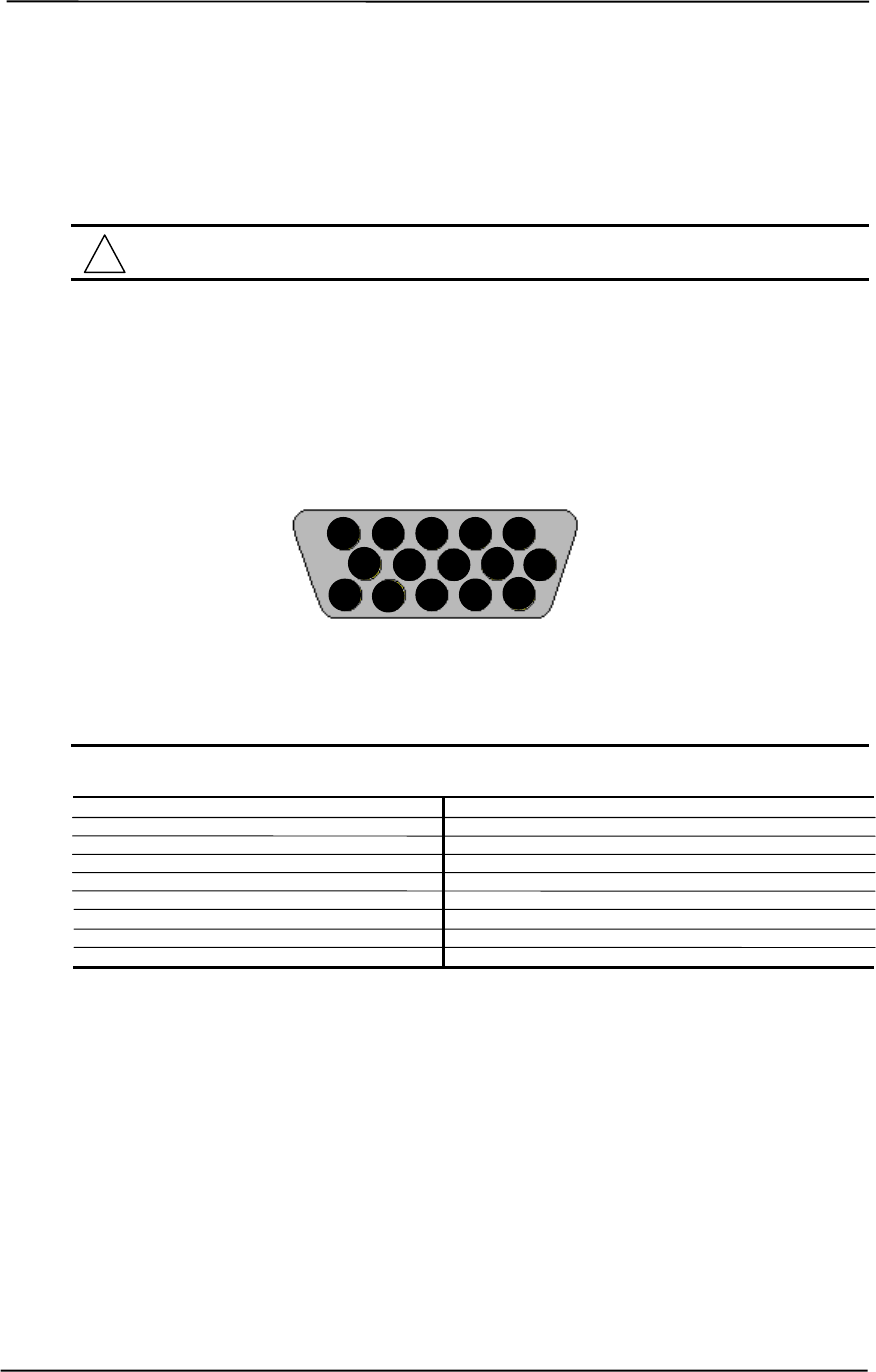
Technical Reference Guide
Compaq Personal Computers
Original - November 2000 E-5
E.6 CONNECTORS
There are two connectors associated with the graphics subsystem; the display/monitor connector
and the Feature connector.
NOTE: The graphic card’s edge connector mates with the AGP slot connector on the
system board. This interface is described in chapter 4 of this guide.
E.6.1 MONITOR CONNECTOR
The display/monitor connector is provided for connection of a compatible RGB/analog monitor.
Figure E-3. VGA Monitor Connector, (Female DB-15, as viewed from rear).
Table E-3. DB-15 Monitor Connector Pinout
Table E-3.
DB-15 Monitor Connector Pinout
Pin Signal Description Pin Signal Description
1 R Red Analog 9 PWR +5 VDC (fused) [1]
2 G Blue Analog 10 GND Ground
3 B Green Analog 11 NC Not Connected
4 NC Not Connected 12 SDA DDC2-B Data
5 GND Ground 13 HSync Horizontal Sync
6 R GND Red Analog Ground 14 VSync Vertical Sync
7 G GND Green Analog Ground 15 SCL DDC2-B Clock
8 B GND Blue Analog Ground -- -- --
NOTES: [1] Fuse automatically resets when excessive load is removed.
15 14 13 12 11
10 9 8 7 6
5 4 3 2 1

Appendix E Compaq/NVIDIA GeForce2 GTS AGP Graphics Card
Compaq Personal Computers
Original - November 2000
E-6
E.6.2 VIDEO FEATURE CONNECTOR
The Video Feature connector allows a video peripheral such as a TV tuner card to provide video
input to the graphics card. This interface is compliant with VESA VIP specification 1.1.
Figure E-4. Feature Connector (26-Pin Header)
Table E–4. Video In Connector Pinout
Table E-4.
Video In Connector Pinout
Pin Signal Description Pin Signal Description
1 / Z1 GND Ground 2 / Y1 P0 Pixel Data 0
3 / Z2 GND Ground 4 / Y2 P1 Pixel Data 1
5 / Z3 GND Ground 6 / Y3 P2 Pixel Data 2
7 / Z4 HAD1 8 / Y4 P3 Pixel Data 3
9 / Z5 HAD0 External Sync 10 / Y5 P4 Pixel Data 4
11 / Z6 HCTL External Clock 12 / Y6 P5 Pixel Data 5
13 / Z7 SCL Serial Clock 14 / Y7 P6 Pixel Data 6
15 / Z8 GND Ground 16 / Y8 P7 Pixel Data 7
17 / Z9 GND Ground 18 / Y9 DCLK Pixel Data Clock
19 / Z10 GND Ground 20 / Y10 NC Not Connected
21 / Z11 GND Ground 22 / Y11 NC Not Connected
23 / Z12 VIRQ 24 / Y12 -- Key
25 / Z13 SDA Serial Data 26 / Y13 GND Ground
2 / Y1
1 / Z1
26 / Y13
25 / Z13
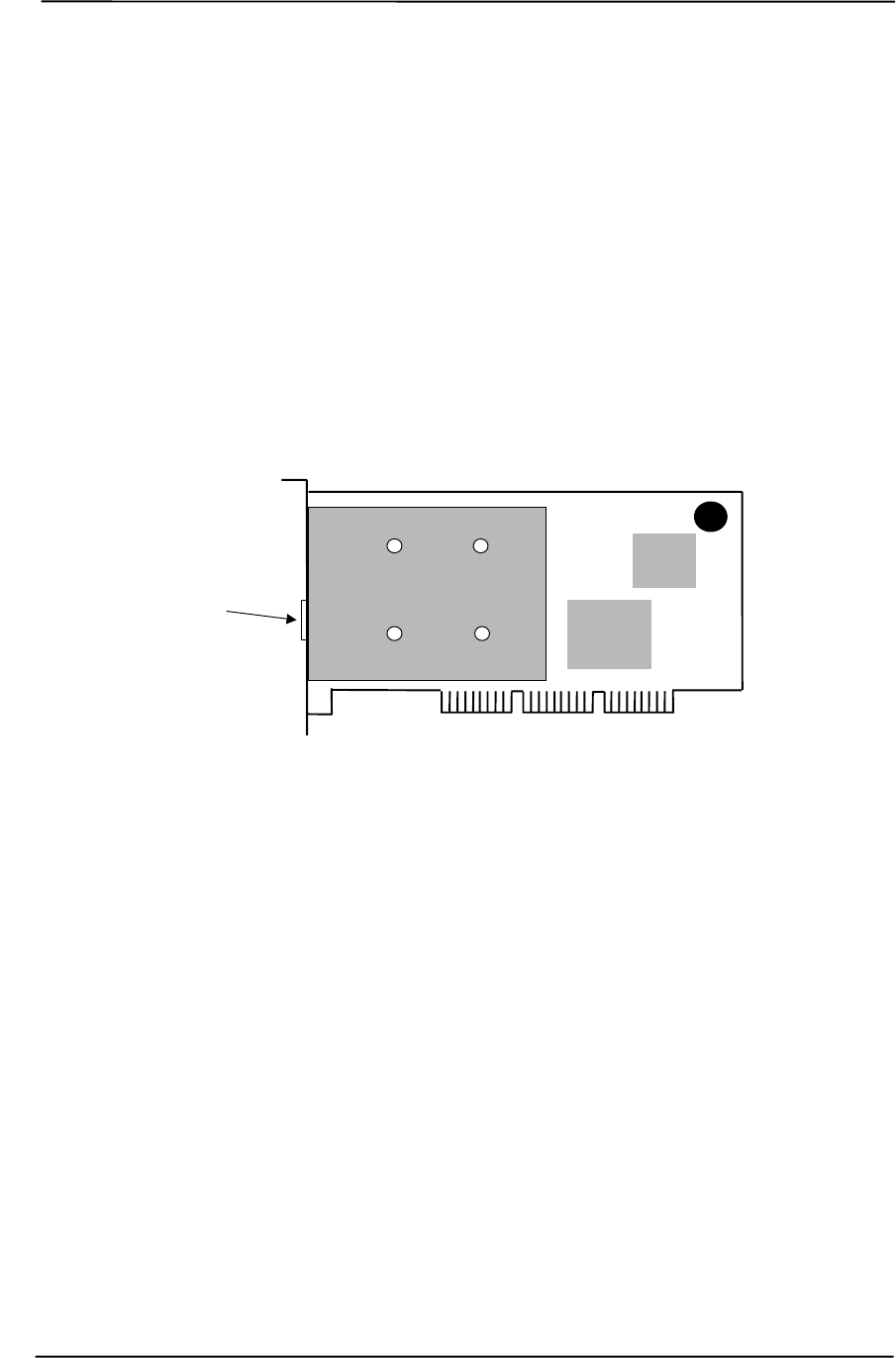
Technical Reference Guide
Compaq Personal Computers
Original - December 2000 F-1
Appendix F
COMPAQ/LUCENT V.90 56K PCI MODEM
F. Appendix F Compaq/Lucent V.90 56K PCI Modem
F.1 INTRODUCTION
This appendix describes the Compaq/Lucent V.90 56K PCI modem (Compaq SP# 146803-001).
This modem installs in a PCI slot, allowing it to be auto-configured into the system.
NOTE: Actual layout may vary.
Figure F-1. Compaq/Lucent V.90 56K PCI Modem (PCA #152972) Layout
This appendix covers the following subjects:
♦ Functional description (F.2) page F-2
♦ Operating parameters (F.3) page F-3
♦ Power management (F.4) page F-4
♦ Programming (F.5) page F-5
♦ Connectors (F.6) page F-5
RJ-11
Connector
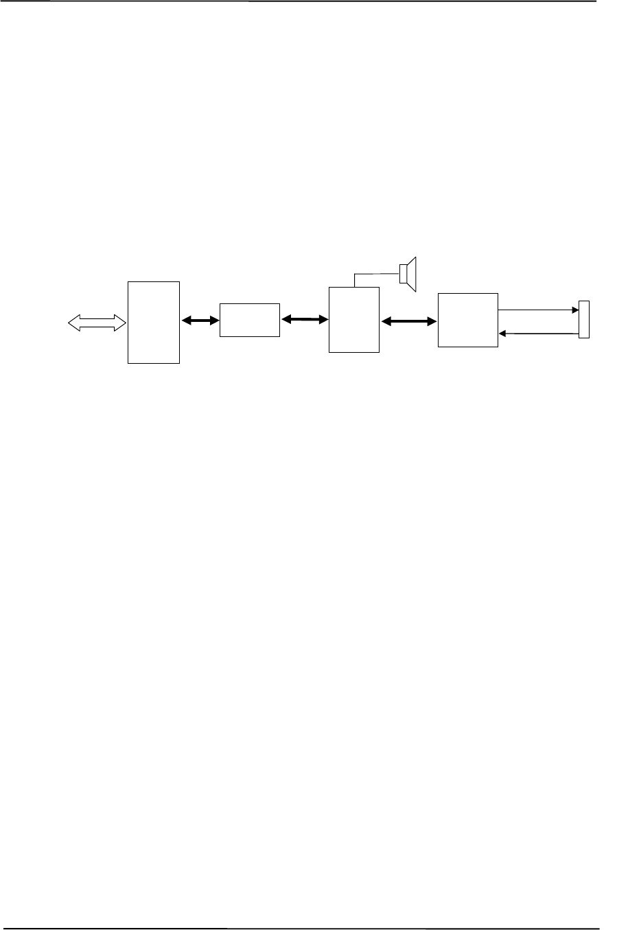
Appendix F Compaq/Lucent V.90 56K PCI Modem
Compaq Personal Computers
Original - December 2000
F-2
F.2 FUNCTIONAL DESCRIPTION
The Compaq/Lucent V.90 56K PCI modem provides data communication over a standard
telephone network at transfer rates of up to 56 kilobits per second. The modem also supports
facsimile (fax) transfers at up to 14.4 kilobits per second. Auto-detection of operating speed and
compression mode is also provided. This modem is of the “controllerless” type, meaning that while
the UART, DSP and DAA functions (Figure F-2) are provided by hardware the operational
functions are largely handled by the modem driver. The modem driver is automatically loaded
upon modem activity and automatically unloaded when the modem activity ceases.
Figure F-2. Compaq/Lucent V.90 56K PCI Modem Block diagram
The Compaq/Lucent V.90 56K PCI Modem includes the following key features:
♦ ITU-T V.90 56 Kbs and K56Flex support w/auto-negotiation of mode
♦ 14400 bps send/receive fax support
♦ ITU-T V.42 error correction (LAPM and MNP)
♦ V.42bis and MNP Class 5 data compression
♦ TIA/EIA 602 standard AT comment set
♦ 115.2 kbps UART speed
♦ PCI 2.2 compliant
♦ PC99 compliant
♦ APM, ACPI power management support
♦ Windows 95, 98, NT4.0 support
Modem operation begins when a program in a virtual machine (VM) attempts to access the com
port designated for the modem’s 16550 UART. A callback procedure is initiated, which loads the
driver that takes over the trapping of the UART’s I/O ports. A background timer is started that
checks for transmit empty / receiver ready states or any other interrupt condition. The com port for
the modem remains open until the DOS VM is terminated. The driver will then unload itself and
the com port will be released.
DAA
Circuitry
DSP
PCI
Bus
Card
Edge
Connector
PCI
I/F
16550
UART
RJ-11
Connector
TX Data
RX Data

Technical Reference Guide
Compaq Personal Computers
Original - December 2000 F-3
F.3 OPERATING PARAMETERS
The operating parameters consists of UART transfer rates and transmission modes.
F.3.1 UART TRANSFER RATES
The transfer rate between the modem’s UART and the PCI interface (also known as the DTE-to-
DCE transfer rate) is selectable and generally set to match the modem’s typical transmission mode.
The modem supports the standard rates of 300, 1200, 2400, 4800, 9600, 14400, 19200, 28800,
38400, 57600, and 115200 bps as well as the high-speed rate of 230400 bps.
F.3.2 TRANSMISSION MODES
The Compaq/Lucent V.90 56K PCI Modem supports the transmission modes listed in table F-1.
Table F-1. Operational Modes
Table F-1.
Operational Modes
Mode Standard Transfer Type Transfer Rate (see text below)
K56Flex (see note) Data 56000, 54000, 52000, 50000, 48000, 46000, 44000,
42000, 40000, 38000, 36000, 34000, 32000 bps
ITU-T V.90 (see note) Data 56000, 54667, 53333, 52000, 50667, 49333, 48000,
46667, 45333, 42667, 41333, 40000, 38667, 37333,
36000, 34667, 33333, 32000, 30667, 29333, 28000
bps
ITU-T V.34Annex12 Data 33600, 31200 bps
ITU-T V.34 Data 28800, 26400, 24000, 21600, 19200, 16800, 14400,
12000, 9600, 7200, 4800 bps
ITU-T V.32bis Data 14400, 12000, 9600, 7200, 4800 bps
ITU-T V.32 Data 9600, 4800 bps
ITU-T V.17 Group 3 Fax 14400, 12000 bps
ITU-T V.29 Group 3 Fax 9600, 7200 bps
ITU-T V.27ter Group 3 Fax 4800, 2400 bps
ITU-T V.22bis Data 2400 bps
ITU-T V.23 Data 1200 / 75 bps
ITU-T V.22 Data 1200 bps
ITU-T V.21 Group 3 Fax 300 bps
BELL 212A Data 1200 baud
BELL 102 Data 300 baud
NOTE: For 56K operation to occur with this device, the following criteria must be met:
- Distant end modem must support 56K modem technology and be digitally terminated.
- Transmission path must contain no more than one analog-to-digital conversion.
The criteria for 56K operation (see note under table F-1) are likely to be met when connecting to
an internet service provider (ISP) through a local phone number. Note also that the 56K transfer
rate applies only to receive data (i.e., “downloads”). Data will be transmitted (“uploaded”) at a
maximum rate of 33.6 Kb/s.

Appendix F Compaq/Lucent V.90 56K PCI Modem
Compaq Personal Computers
Original - December 2000
F-4
F.4 POWER MANAGEMENT
The modem supports both APM and ACPI power management environments using methods
defined in the PCI 2.2 specification.
F.4.1 APM ENVIRONMENT
In the APM environment, the modem will be placed in Standby (as the result of either a user-
initiated action or by OS timer) unless the modem is online or transferring data. If a thermal
shutdown condition occurs, then the modem will be forced into Standby regardless of the
operational state.
F.4.2 ACPI ENVIRONMENT
The modem supports the ACPI power management environment and is compliant with PCI
specification 2.2 (PME- signaling). The card can provide system wake-up from a ring condition .
F.5 PROGRAMMING
The Compaq/Lucent V.90 56K PCI Modem card is a “controllerless” modem, meaning that all
operating parameters are controlled by the modem driver. Modem updates (if any) will be
facilitated only through the driver. Flash ROM is not involved. The modem is identified on the PCI
bus with the following values:
Vender ID (PCI Configuration space address 00h): 11C1h
Device ID (PCI Configuration space address 02h): 0441h
F.6 CONNECTOR
The card includes an RJ-11 connector for connection to an analog phone line. The signal is carried
on the two center conductors.
Figure F-3. RJ-11 Connector, (Female, as viewed from rear).
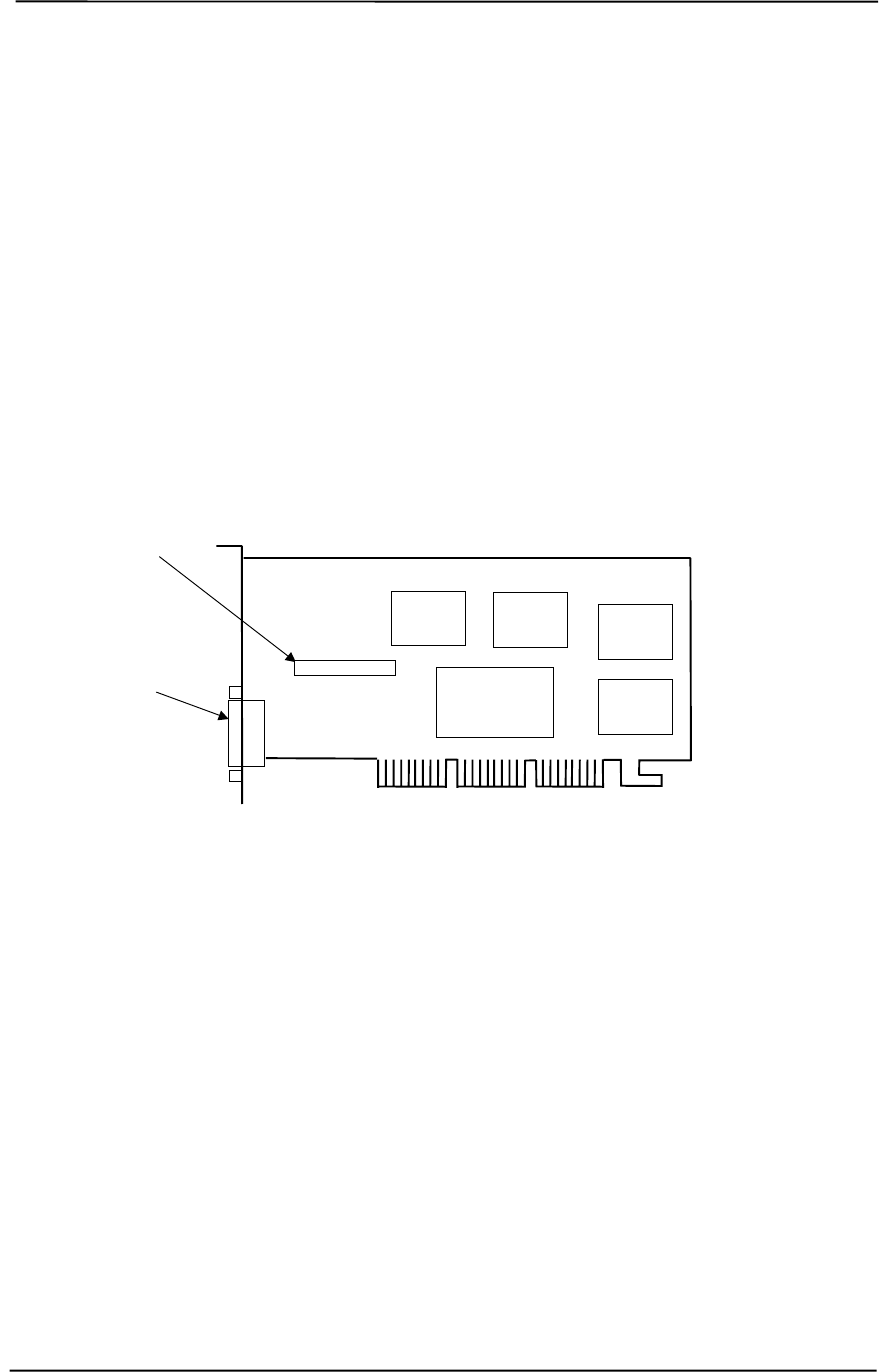
Technical Reference Guide
Compaq Personal Computers
Original - November 2000 G-1
Appendix G
COMPAQ/ELSA Gloria II
AGP GRAPHICS CARD
G. Appendix G Compaq/ELSA Gloria II Graphics Card
G.1 INTRODUCTION
This appendix describes the Compaq/ELSA GLoria II AGP Graphics Card used in the standard
configuration on some models and also available as an option. This card (layout shown in the
following figure) installs in a system’s AGP slot. The Compaq/ELSA GLoria II graphics card
(P/N 174565-001) provides high 2D performance as well as mid-level 3D capabilities.
Figure G-1. Compaq/ELSA GLoria II AGP Graphics Card (P/N 174565-001) Layout
This appendix covers the following subjects:
♦ Functional description (D.2) page D-2
♦ Display modes (D.3) page D-3
♦ Software support information (D.4) page D-4
♦ Monitor power management (D.5) page D-4
♦ Connectors (D.6) page D-5
Feature Connector
NVIDIA
NV10 Quadro
Controller SDRAM
SDRAM
SDRAM SDRAM
RGB Monitor
Connector

Appendix G Compaq/ELSA GLoria II AGP Graphics Card
Compaq Personal Computers
Original - November 2000
G-2
G.2 FUNCTIONAL DESCRIPTION
The ELSA GLoria II-SD Graphics Card provides high performance 2D and 3D display imaging.
The card’s AGP design provides an economical approach to 3D processing by off-loading 3D
effects such as texturing, z-buffering and alpha blending to the system memory while 64 megabytes
of on-board SDRAM stores the main display image.
Figure G-2. ELSA GLoria II Graphics Card Block diagram
The ELSA GLoria II Graphics Card includes the following features:
♦ 64-MB SDRAM frame buffer using 128-bit 166-MHz access
♦ AGP 4X transfers with sideband addressing
♦ 2D drawing engine with:
• 128-bit BitBLTs, rectangle/polygon fills, line draws
• Hardware cursor
• 8-/16-/32-bpp mode acceleration
♦ DVD support with:
• Hardware-accelerated MPEG2 (720 x 480)
• HDTV format support (720i-1080i, 720p-1080p)
♦ 3D accelerator with:
• Hardware transform and lighting
• Single-pass dual textures
• 4 rendering pipelines
• Anistropic filtering
• 8-bit stencil buffer
• Specular lighting diffuse shading
• 16-/24-bit Z-buffering
♦ 350-MHz RAMDAC
♦ VESA compliancy:
• DVI/DFP connector
• DDC2B monitor support
• DPMS, EPA Energy Star, and ACPI-compliant power management
BIOS
ROM
HSync
128-bit
166-MHz
Data Bus
Analog
Monitor
Connector
RGB
NVIDIA N10 Graphics Controller
3D Array
Engine
Video
Scalar
350-MHz
RAM
DAC
CRT
Controller
Memory
I/F
AGP
Bus
Card
Edge
Connector VSync
2D/VGA
Engine
64 MB
SDRAM
Frame Buffer
AGP 4X
I/F

Technical Reference Guide
Compaq Personal Computers
Original - November 2000 G-3
G.3 DISPLAY MODES
The graphics display modes supported by the ELSA GLoria II Graphics are listed in Table G-1.
Table G-1. ELSA GLoria II Graphics Display Modes
Table G-1.
ELSA GLoria II Graphics Display Modes
Resolution Bits per pixel Color Depth Max. Vertical
Refresh Freq. [1] Memory Used
For Texture
640 x 480 8 256 120 64.3 MB
640 x 480 16 65K 120 63.7 MB
640 x 480 32 16.7M 120 61.9 MB
800 x 600 8 256 120 63.6 MB
800 x 600 16 65K 120 62.7 MB
800 x 600 32 16.7M 120 59 9 MB
1024 x 768 8 256 120 62.4 MB
1024 x 768 16 65K 120 60.9 MB
1024 x 768 32 16.7M 120 56.2 MB
1152 x 864 8 256 100 61.6 MB
1152 x 864 16 65K 100 59.7 MB
1152 x 864 32 16.7M 100 53.8 MB
1280 x 1024 8 256 100 60.4 MB
1280 x 1024 16 65K 100 57.9 MB
1280 x 1024 32 16.7M 100 50.2 MB
1536 x 960 8 256 100 59.8 MB
1536 x 960 16 65K 100 56.9 MB
1536 x 960 32 16.7M 100 48.3 MB
1600 x 1000 8 256 85 59.3 MB
1600 x 1000 16 65K 85 56.2 MB
1600 x 1000 32 16.7M 85 46.8 MB
1600 x 1200 8 256 85 58.0 MB
1600 x 1200 16 65K 85 54.3 MB
1600 x 1200 32 16.7M 75 43.0 MB
1600 x 1280 8 256 85 57.3 MB
1600 x 1280 16 65K 85 53.5 MB
1600 x 1280 32 16.7M 75 41.5 MB
1792 x 1120 8 256 85 57.7 MB
1792 x 1120 16 65K 85 53.8 MB
1792 x 1120 32 16.7M 75 42.0 MB
1920 x 1080 8 256 85 57.4 MB
1920 x 1080 16 65K 85 53.4 MB
1920 x 1080 32 16.7M 75 41.2 MB
1920 x 1200 8 256 85 56.5 MB
1920 x 1200 16 65K 75 52.0 MB
1920 x 1200 32 16.7M 75 38.5 MB
NOTE: [1] Value reflects hardware capabilities only. May be restricted by operating system.

Appendix G Compaq/ELSA GLoria II AGP Graphics Card
Compaq Personal Computers
Original - November 2000
G-4
G.4 SOFTWARE SUPPORT INFORMATION
The ELSA GLoria II graphics card is fully compatible with software written for legacy video
modes (VGA, EGA, CGA) and needs no driver support for those modes.
Drivers are provided with or available for the card to provide extended mode support for the
current operating systems and programming environments such as:
♦ Windows 2000
♦ Windows NT 4.0
♦ Autodesk AutoCAD R14 and 2000
♦ Kintex 3D Studio Max
♦ 2D GDI
♦ MS DirectDraw DX6-7, ActiveX, DirectX, Direct3D,
♦ OpenGL 1.1 and 1.2
PCI bus configuration data:
Vendor ID: 10DEh
Device ID: 0150h
G.5 POWER MANAGEMENT AND CONSUMPTION
This controller provides monitor power control for monitors that conform to the VESA display
power management signaling (DPMS) protocol. This protocol defines different power
consumption conditions and uses the HSYNC and VSYNC signals to select a monitor’s power
condition. Table G-2 lists the monitor power conditions.
Table G-2. Monitor Power Management Conditions
Table G-2.
Monitor Power Management Conditions
HSYNC VSYNC Power Mode Description
Active Active On Monitor is completely powered up. If activated, the inactivity
counter counts down during system inactivity and if allowed to
tiemout, generates an SMI to initiate the Suspend mode.
Active Inactive Suspend Monitor’s high voltage section is turned off and CRT heater
(filament) voltage is reduced from 6.6 to 4.4 VDC. The Off mode
inactivity timer counts down from the preset value and if allowed
to timeout, another SMI is generated and serviced, resulting in
the monitor being placed into the Off mode. Wake up from
Suspend mode is typically a few seconds.
Inactive Inactive Off Monitor’s high voltage section and heater circuitry is turned off.
Wake up from Off mode is a little longer than from Suspend.

Technical Reference Guide
Compaq Personal Computers
Original - November 2000 G-5
G.6 CONNECTORS
There are two connectors associated with the graphics subsystem; the display/monitor connector
and the Feature connector.
NOTE: The graphic card’s edge connector mates with the AGP slot connector on the
system board. This interface is described in chapter 4 of this guide.
G.6.1 MONITOR CONNECTOR
The display/monitor connector is provided for connection of a compatible RGB/analog monitor.
Figure G-3. VGA Monitor Connector, (Female DB-15, as viewed from rear).
Table G-3. DB-15 Monitor Connector Pinout
Table G-3.
DB-15 Monitor Connector Pinout
Pin Signal Description Pin Signal Description
1 R Red Analog 9 PWR +5 VDC (fused) [1]
2 G Blue Analog 10 GND Ground
3 B Green Analog 11 NC Not Connected
4 NC Not Connected 12 SDA DDC2-B Data
5 GND Ground 13 HSync Horizontal Sync
6 R GND Red Analog Ground 14 VSync Vertical Sync
7 G GND Green Analog Ground 15 SCL DDC2-B Clock
8 B GND Blue Analog Ground -- -- --
NOTES: [1] Fuse automatically resets when excessive load is removed.
15 14 13 12 11
10 9 8 7 6
5 4 3 2 1

Appendix G Compaq/ELSA GLoria II AGP Graphics Card
Compaq Personal Computers
Original - November 2000
G-6
G.6.2 VIDEO FEATURE CONNECTOR
The Video Feature connector allows a video peripheral such as a TV tuner card to provide video
input to the graphics card. This interface is compliant with VESA VIP specification 1.1.
Figure G-4. Feature Connector (26-Pin Header)
Table G–4. Video In Connector Pinout
Table G-4.
Video In Connector Pinout
Pin Signal Description Pin Signal Description
1 / Z1 GND Ground 2 / Y1 P0 Pixel Data 0
3 / Z2 GND Ground 4 / Y2 P1 Pixel Data 1
5 / Z3 GND Ground 6 / Y3 P2 Pixel Data 2
7 / Z4 HAD1 8 / Y4 P3 Pixel Data 3
9 / Z5 HAD0 External Sync 10 / Y5 P4 Pixel Data 4
11 / Z6 HCTL External Clock 12 / Y6 P5 Pixel Data 5
13 / Z7 SCL Serial Clock 14 / Y7 P6 Pixel Data 6
15 / Z8 GND Ground 16 / Y8 P7 Pixel Data 7
17 / Z9 GND Ground 18 / Y9 DCLK Pixel Data Clock
19 / Z10 GND Ground 20 / Y10 NC Not Connected
21 / Z11 GND Ground 22 / Y11 NC Not Connected
23 / Z12 VIRQ 24 / Y12 -- Key
25 / Z13 SDA Serial Data 26 / Y13 GND Ground
2 / Y1
1 / Z1
26 / Y13
25 / Z13
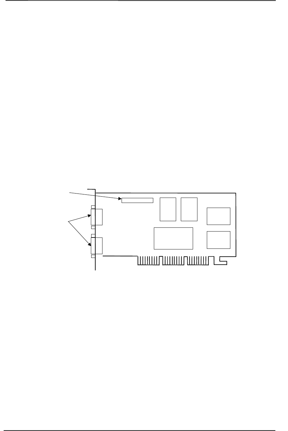
Technical Reference Guide
Compaq Personal Computers
Original - November 2000 H-1
Appendix H
COMPAQ/Matrox Millennium G450
AGP GRAPHICS CARD
H. Appendix G Compaq/Matrox Millennium G450 AGP Graphics
Card
H.1 INTRODUCTION
This appendix describes the Compaq/Matrox Millennium G450 AGP Graphics Card used in the
standard configuration on some models and also available as an option. This card (layout shown in
the following figure) installs in a system’s AGP slot. The Compaq/Matrox Millennium G450
graphics card (SP# 203626-001) provides high 2D performance and entry-level 3D capabilities.
This card features a dual-RAMDAC design for driving two analog displays.
Figure H-1. Compaq/Matrox Millennium G450 AGP Graphics Card Layout (PCA# 202901-001)
This appendix covers the following subjects:
♦ Functional description (D.2) page D-2
♦ Display modes (D.3) page D-3
♦ Software support information (D.4) page D-4
♦ Monitor power management (D.5) page D-4
♦ Connectors (D.6) page D-5
Feature Connector
MGA
Dual-RAMDAC
Controller SDRAM
SDRAM
SD
RAMRGB Monitor
Connectors
SD
RAM
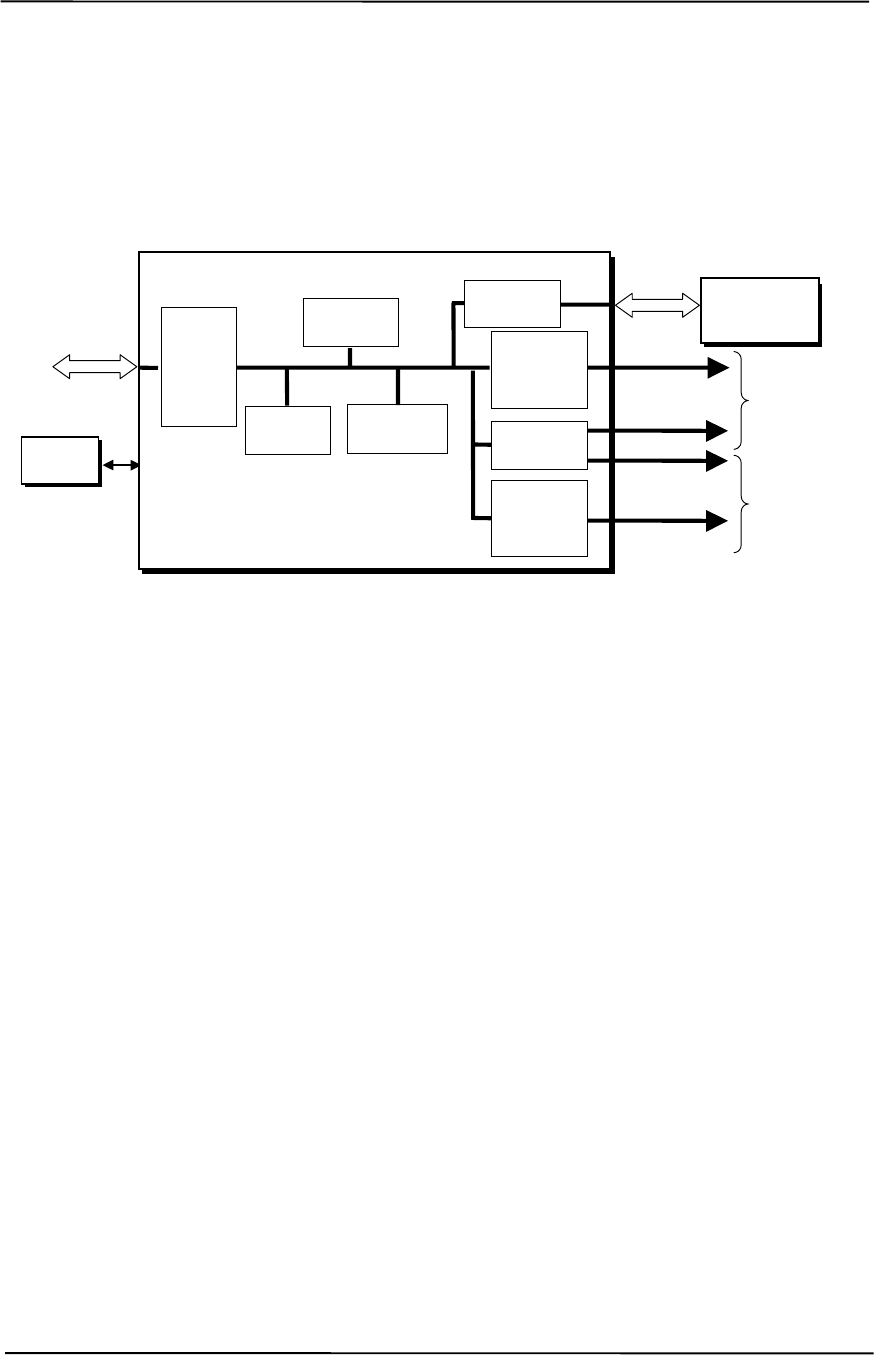
Appendix H Compaq/Matrox Millennium G450 AGP Graphics Card
Compaq Personal Computers
Original - November 2000
H-2
H.2 FUNCTIONAL DESCRIPTION
The Matrox Millennium G450-SD Graphics Card provides high performance 2D and 3D display
imaging. The card’s AGP design provides an economical approach to 3D processing by off-
loading 3D effects such as texturing, z-buffering and alpha blending to the system memory while
32 megabytes of on-board SDRAM stores the main display image.
Figure H-2. Matrox Millennium G450 Graphics Card Block diagram
The Matrox Millennium G450 Graphics Card includes the following features:
♦ 64-MB SDRAM frame buffer using 128-bit 166-MHz access
♦ AGP 4X transfers with sideband addressing
♦ 2D drawing engine with:
• 128-bit BitBLTs, rectangle/polygon fills, line draws
• Hardware cursor
• 8-/16-/32-bpp mode acceleration
♦ Dual-head features:
• Two analog monitor (RGB) ports
• DVD max mode
• DualHead zoom mode
• DualHead clone mode
• DualHead TV output mode
♦ 3D accelerator with:
• Hardware transform and lighting
• Anistropic filtering
• Specular lighting diffuse, flat and Gouraud shading
• 16-/24-bit Z-buffering
♦ 360-MHz primary RAMDAC, 200-MHz secondary RAMDAC
♦ VESA compliancy:
• Dual DDC2B monitor support
• VIP 2.0 interface
• DPMS, EPA Energy Star, and ACPI-compliant power management
BIOS
ROM
128-bit
166-MHz
Data Bus
Analog
Monitor
Connector 1
RGB
MGA Graphics Controller
3D Array
Engine
Video
Scalar
AGP
Bus
Card
Edge
Connector
H/VSync
2D/VGA
Engine
32 MB
SDRAM
Frame Buffer
AGP 4X
I/F 350-MHz
RAMDAC
CRT
Controller
RGB
Analog
Monitor
Connector 2
200-MHz
RAMDAC
H/VSync
Memory
I/F

Technical Reference Guide
Compaq Personal Computers
Original - November 2000 H-3
H.3 DISPLAY MODES
The graphics display modes supported by the Matrox Millennium G450 Graphics are listed in
Table H-1.
Table H-1. Matrox Millennium G450 Graphics Display Modes
Table H-1.
Matrox Millennium G450 Graphics Display Modes
Resolution Bits per pixel Color Depth Max. Vertical
Refresh Freq. [1] Supporting
RAMDAC
640 x 480 8 256 85 Hz Primary
640 x 480 16 65K 85 Hz Primary, Secondary
640 x 480 24 16.7M 85 Hz Primary
640 x 480 32 16.7M 85 Hz Primary, Secondary
800 x 600 8 256 85 Hz Primary
800 x 600 16 65K 85 Hz Primary, Secondary
800 x 600 24 16.7M 85 Hz Primary
800 x 600 32 16.7M 85 Hz Primary, Secondary
1024 x 768 8 256 85 Hz Primary
1024 x 768 16 65K 85 Hz Primary, Secondary
1024 x 768 24 16.7M 85 Hz Primary
1024 x 768 32 16.7M 85 Hz Primary, Secondary
1152 x 864 8 256 75 Hz Primary
1152 x 864 16 65K 75 Hz Primary, Secondary
1152 x 864 24 16.7M 75 Hz Primary
1152 x 864 32 16.7M 75 Hz Primary, Secondary
1280 x 960 8 256 85 Hz Primary
1280 x 960 16 65K 85 Hz Primary, Secondary
1280 x 960 24 16.7M 85 Hz Primary
1280 x 960 32 16.7M 85 Hz Primary, Secondary
1280 x 1024 8 256 85 Hz Primary
1280 x 1024 16 65K 85 Hz Primary, Secondary
1280 x 1024 24 16.7M 85 Hz Primary
1280 x 1024 32 16.7M 85 Hz Primary, Secondary
1600 x 1200 8 256 85 Hz Primary
1600 x 1200 16 65K 85 Hz Primary, Secondary
1600 x 1200 24 16.7M 85 Hz Primary
1600 x 1200 32 16.7M 85 Hz Primary, Secondary
1800 x 1440 8 256 85 Hz Primary
1800 x 1440 16 65K 85 Hz Primary
1800 x 1440 24 16.7M 85 Hz Primary
1856 x 1392 8 256 85 Hz Primary
1856 x 1392 16 65K 85 Hz Primary
1856 x 1392 24 16.7M 85 Hz Primary
1920 x 1440 8 256 85 Hz Primary
1920 x 1440 16 65K 85 Hz Primary
1920 x 1440 24 16.7M 85 Hz Primary
2048 x 768 8 256 75 Hz Primary
2048 x 768 16 65K 75 Hz Primary
NOTE: [1] Value reflects hardware capabilities only. May be restricted by operating system.

Appendix H Compaq/Matrox Millennium G450 AGP Graphics Card
Compaq Personal Computers
Original - November 2000
H-4
H.4 SOFTWARE SUPPORT INFORMATION
The Matrox Millennium G450 graphics card is fully compatible with software written for legacy
video modes (VGA, EGA, CGA) and needs no driver support for those modes.
Drivers are provided with or available for the card to provide extended mode support for the
current operating systems and programming environments such as:
♦ Windows 2000
♦ Windows NT 4.0
♦ Autodesk AutoCAD R14 and 2000
♦ Kintex 3D Studio Max
♦ 2D GDI
♦ MS DirectDraw DX6-7, ActiveX, DirectX, Direct3D,
♦ OpenGL 1.1 and 1.2
H.5 POWER MANAGEMENT AND CONSUMPTION
This controller provides monitor power control for monitors that conform to the VESA display
power management signaling (DPMS) protocol. This protocol defines different power
consumption conditions and uses the HSYNC and VSYNC signals to select a monitor’s power
condition. Table H-2 lists the monitor power conditions.
Table H-2. Monitor Power Management Conditions
Table H-2.
Monitor Power Management Conditions
HSYNC VSYNC Power Mode Description
Active Active On Monitor is completely powered up. If activated, the inactivity
counter counts down during system inactivity and if allowed to
tiemout, generates an SMI to initiate the Suspend mode.
Active Inactive Suspend Monitor’s high voltage section is turned off and CRT heater
(filament) voltage is reduced from 6.6 to 4.4 VDC. The Off mode
inactivity timer counts down from the preset value and if allowed
to timeout, another SMI is generated and serviced, resulting in
the monitor being placed into the Off mode. Wake up from
Suspend mode is typically a few seconds.
Inactive Inactive Off Monitor’s high voltage section and heater circuitry is turned off.
Wake up from Off mode is a little longer than from Suspend.

Technical Reference Guide
Compaq Personal Computers
Original - November 2000 H-5
H.6 CONNECTORS
There are three connectors associated with the graphics subsystem; two display/monitor connectors
and the Feature connector.
NOTE: The graphic card’s edge connector mates with the AGP slot connector on the
system board. This interface is described in chapter 4 of this guide.
H.6.1 MONITOR CONNECTOR
The display/monitor connector is provided for connection of a compatible RGB/analog monitor.
Figure H-3. VGA Monitor Connector, (One of two female DB-15, as viewed from rear).
Table H-3. DB-15 Monitor Connector Pinout
Table H-3.
DB-15 Monitor Connector Pinout
Pin Signal Description Pin Signal Description
1 R Red Analog 9 PWR +5 VDC (fused) [1]
2 G Blue Analog 10 GND Ground
3 B Green Analog 11 NC Not Connected
4 NC Not Connected 12 SDA DDC2-B Data
5 GND Ground 13 HSync Horizontal Sync
6 R GND Red Analog Ground 14 VSync Vertical Sync
7 G GND Green Analog Ground 15 SCL DDC2-B Clock
8 B GND Blue Analog Ground -- -- --
NOTES: [1] Fuse automatically resets when excessive load is removed.
15 14 13 12 11
10 9 8 7 6
5 4 3 2 1

Appendix H Compaq/Matrox Millennium G450 AGP Graphics Card
Compaq Personal Computers
Original - November 2000
H-6
H.6.2 VIDEO FEATURE CONNECTOR
The Video Feature connector allows a video peripheral such as a TV tuner card to provide video
input to the graphics card. This interface is compliant with VESA VIP specification 1.1.
Figure H-4. Feature Connector (26-Pin Header)
Table H–4. Video In Connector Pinout
Table G-4.
Video In Connector Pinout
Pin Signal Description Pin Signal Description
1 / Z1 GND Ground 2 / Y1 P0 Pixel Data 0
3 / Z2 GND Ground 4 / Y2 P1 Pixel Data 1
5 / Z3 GND Ground 6 / Y3 P2 Pixel Data 2
7 / Z4 HAD1 8 / Y4 P3 Pixel Data 3
9 / Z5 HAD0 External Sync 10 / Y5 P4 Pixel Data 4
11 / Z6 HCTL External Clock 12 / Y6 P5 Pixel Data 5
13 / Z7 SCL Serial Clock 14 / Y7 P6 Pixel Data 6
15 / Z8 GND Ground 16 / Y8 P7 Pixel Data 7
17 / Z9 GND Ground 18 / Y9 DCLK Pixel Data Clock
19 / Z10 GND Ground 20 / Y10 NC Not Connected
21 / Z11 GND Ground 22 / Y11 NC Not Connected
23 / Z12 VIRQ 24 / Y12 -- Key
25 / Z13 SDA Serial Data 26 / Y13 GND Ground
2 / Y1
1 / Z1
26 / Y13
25 / Z13
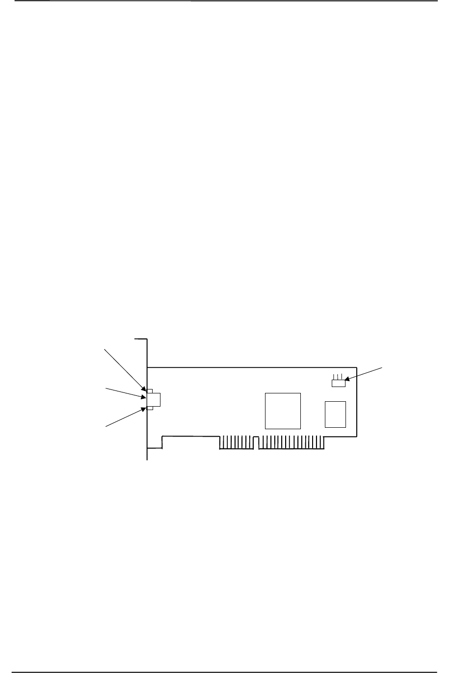
Technical Reference Guide
Compaq Personal Computers
Original - December 2000 I-1
Appendix I
COMPAQ/INTEL
NETWORK INTERFACE CONTROLLER ADAPTERS
I. Appendix I Compaq/Intel Network Interface Controller
Adapters
I.1 INTRODUCTION
This appendix describes Compaq/Intel Network Interface Controller adapters that may be included
in the standard configuration on some models and available as options for all models. This
appendix describes the following devices:
♦ Compaq/Intel PRO/100+ Management Adapter (SP# 116188-001)
♦ Compaq/Intel PRO/100 S Management Adapter (SP# 215774-001)
Each adapter card installs in a PCI slot to provide a system with network interface capability.
Unless otherwise indicated, the following information applies to both adapter cards.
NOTES: PRO/100+ Management Adapter, PCA# 108897
PRO/100 S Management Adapter, PCA# 213464
Figure I-1. Intel PRO/100+ or PRO/100 S Management Adapter Card Layout
This appendix covers the following subjects:
♦ Functional description (I.2) page I-2
♦ Power management (I.3) page I-4
♦ Adapter programming (I.4) page I-5
♦ Network connector (I.5) page I-6
♦ Adapter specifications (I.6) page I-6
Link/Activity
LED
RJ-45
Network
Connector
Speed
LED
825xx
NIC
WOL
Connector
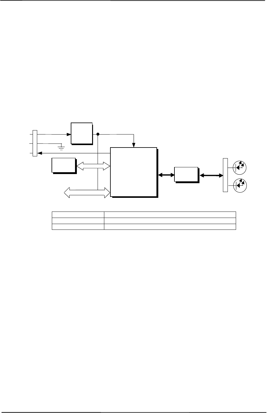
Appendix I Compaq/Intel Network Interface Controller Adapters
Compaq Personal Computers
Original - December 2000
I-2
I.2 FUNCTIONAL DESCRIPTION
The Intel PRO/100+ and the PRO/100 S Management Adapters are based on the Intel 82559 and
82550 Ethernet Controllers (respectively) supported by firmware in flash ROM (Figure I-2). Each
adapter can operate in half- or full-duplex modes and provides auto-negotiation of both mode and
speed. Half-duplex operation features an Intel-proprietary collision reduction mechanism while
full-duplex operation follows the IEEE 802.3x flow control specification. Transmit and receive
FIFOs of three kilobytes each reduce the chance of overrun while waiting for bus access. Each
card includes an on-board 5/3.3 VDC regulator circuit and WOL connector in support of Wake-
On-LAN functionality.
Controller Type Featured on
82559 Intel PRO/100+ Management Adapter
82550 Intel PRO/100 S Management Adapter
Figure I-2. Intel PRP/100+ Management Adapter, Block diagram
Key features of these adapters include:
♦ 3-KB transmit and 3-KB receive FIFOs
♦ PCI ver. 2.2 compliant (PME- support)
♦ Dual-mode support with auto-switching between 10BASE-T and 100BASE-TX
♦ Both APM and ACPI power management support
♦ D0-D3 power state wake event support
♦ Boot ROM with PXE and RPL support
The 82559 and 82550 controllers feature high and low priority queues and provides priority-packet
processing for networks that support that feature. The controller’s micro-machine processes
transmit and receive frames independently and concurrently. Receive runt (undersized) frames are
not passed on as faulty data but discarded by the controller, which also directly handles such errors
as collision detection or data under-run. An EEPROM is used to store identification, configuration,
and connection parameters.
The 82550 controller provides all the functionality of the 82559 plus IP security (IPSEC) support
through a hardware accelerator engine.
WOL
Conn.
Intel
825xx
Ethernet Controller
(see table below)
32-Bit
PCI
PCI
Connector
5/3.3
VDC
Reg.
BIOS
ROM TX/RX Speed
RJ-45
Conn.
TX/RX
PHY
Link/
Activit
y
WOL
GND
5 VDC Aux 3.3 VDC
1
2
3

Technical Reference Guide
Compaq Personal Computers
Original - December 2000 I-3
I.2.1 AOL FUNCTION
The adapter’s Alert-On-LAN (AOL) function provides a AOL-compliant system unit with the
ability to communicate system status to a management console, even while the system is powered
down. When installed in an AOL-compliant system, the adapter receives alert messages from the
system’s I/O Controller Hub (ICH) over the PCI bus. Each alert message decoded by the adapter
results in a pre-constructed status message being transmitted over the network to a management
console.
Alert-On-LAN functionality occurs independent of software, driver, or even processor
intervention. The adapter can report following conditions:
♦ System tampering – Removal of the chassis cover
♦ BIOS failure – System fails to boot successfully
♦ OS problem – System fails to load operating system after boot
♦ Missing/faulty processor – Processor fails to fetch first instruction
♦ Thermal condition – High temperature detected in system
♦ Heartbeat – Indication of system’s presence on the network (sent approximately every 30
seconds)
NOTE: The system unit must be plugged into a live AC outlet for the AOL function to be
operative. Controlling a system unit’s power through an AC outlet strip will, when
the strip is turned off, disable AOL functionality.
The AOL implementation requirements are as follows:
1. System unit featuring the 810, 810e, 820, or 850 (or later) chipset.
2. Intel PRO/100+ Management Adapter Driver 3.1 or later (available from Compaq).
3. Client-side utility agent software (available from Compaq).
4. Management console running one of the following:
a. HP OpenView Network Node Manager 6.x.
b. Intel LANDesk Client Manager.
c. Compaq Insight Manager.
I.2.2 WAKE UP FUNCTIONS
The adapter provides two types of wake-up signaling: the PME- signal and the WOL signal.
The adapter provides PME- signal support for systems compliant with PCI ver. 2.2. The detection
of any wake event results in the adapter’s assertion of the PME- signal, which can be used by the
system unit to initiate the power-up sequence. System software is responsible for the clearing the
PME- signal.
The adapter also includes a WOL interface for systems supporting that method of wake-up. The
adapter asserts the WOL signal for 50 milliseconds upon detection of a Magic Packet. The WOL
signal is routed to the system unit (through a three-conductor cable connection) for initializing a
power-up sequence.

Appendix I Compaq/Intel Network Interface Controller Adapters
Compaq Personal Computers
Original - December 2000
I-4
I.2.3 IPSEC FUNCTION
The 82550 controller used on the Intel PRO/100 S Management Adapter includes an encryption
engine that provides on-the-fly encryption and/or authentication of transmit data without additional
use of system memory and software. This function, referred to as IP security (IPSEC), uses a
configurable algorithm and established Data Encryption Standards (DES) to provide high
performance (full transmission rate) encryption. Received IPSEC data frames are re-submitted to
the controller for processing and then returned to the driver.
Key features of IPSEC support include:
♦ Encryption capability of 56-bit DES to 168-bit 3DES
♦ Out-of-order processing of non-security transmit frames during security mode
♦ SHA-1 and MD-5 authentication with optional HMAC cryptographic hashing

Technical Reference Guide
Compaq Personal Computers
Original - December 2000 I-5
I.3 POWER MANAGEMENT SUPPORT
These adapters support APM and ACPI power management environments as well as the Wired-
for-Management (WfM) and Wake-On-LAN (WOL) standards. The adapter is designed to be
powered up as long as the system unit is plugged into a live AC outlet to provide system “wake-
up” functionality. Power is provided by either the auxiliary 3.3 VDC power rail of the PCI bus
(when installed in systems compliant with PCI ver. 2.2) or by auxiliary 5 VDC through the WOL
connector.
NOTE: Controlling a system unit’s power through an AC outlet strip will, with the strip
turned off, disable wake-up functionality.
I.3.1 APM ENVIRONMENT
The Advanced Power Management (APM) functionality of system wake up is implemented
through the system’s APM-compliant BIOS and Magic Packet-compliant hardware. This
environment is not dependent on operating system (OS) intervention allowing a unit plugged into a
live AC outlet to be turned on remotely over the network (i.e., “remote wake-up”) even if the OS
has not been installed. In APM mode the controller will respond upon receiving a Magic Packet,
which is a packet where the node’s address is repeated 16 times. Upon Magic Packet reception, the
adapter asserts the PME- signal (on the PCI bus) resulting in the system unit’s power control logic
turning on the system and initiating the boot sequence. After the boot sequence the BIOS clears
the PME- signal so that subsequent wake up events will be detected.
I.3.2 ACPI ENVIRONMENT
The Advanced Configuration and Power Interface (ACPI) functionality of system wake up is
implemented through an ACPI-compliant OS (such as Windows NT 5.0) and is the default power
management mode. The following wake up events may be individually enabled/disabled through
the software driver supplied with the adapter:
♦ Magic Packet – Packet with node address repeated 16 times in data portion.
♦ Individual address match – Directed acket with matching user-defined byte mask.
♦ Multicast address match – Directed packet with matching user-defined sample frame.
♦ ARP (address resolution protocol) packet
♦ Flexible packet filtering – Packets that match defined CRC signature.
♦ NBT query (under Ipv4)
♦ IPX Diagnostic
♦ TCO packet
♦ VLAN Type
When an enabled event is received the controller asserts the PME- signal that is used to initiate the
wakeup sequence.

Appendix I Compaq/Intel Network Interface Controller Adapters
Compaq Personal Computers
Original - December 2000
I-6
I.4 ADAPTER PROGRAMMING
Programming the adapter consists of configuration, which occurs during POST, and control, which
occurs at runtime.
I.4.1 CONFIGURATION
The adapter’s 82559 or 82550 NIC controller is a PCI device and configured though PCI
configuration space registers using PCI protocol described in chapter 4 of this guide. The PCI
configuration registers are listed in the following table:
Table I-1. NIC Controller PCI Configuration Registers
Table I-1.
PCI Configuration Registers
PCI
Conf.
Addr. Register
Value
on
Reset
PCI
Conf.
Addr. Register
Value
on
Reset
00-01h Vender ID 8086h 10-13h Cntrl. Reg. Base Addr. (Mem) 0000h
02-03h Device ID 1229h 14-17h Cntrl. Reg. Base Addr. (I/O) 00h
04-05h PCI Command 0000h 18-1Bh Flash Mem. Base Addr. 00h
06-07h PCI Status 0280h 2C-2Dh Subsystem Vender ID
08h Revision ID xxh 2E-2Fh Subsystem ID
09-0Bh Class Code 01h 30-33h Expansion ROM Base Addr.
0Ch Cache Line Size 01h 34h Cap-Ptr
0Dh Latency Timer 04h 3C-3D Interrupt Line/Pin
0Eh Header Type 00h 3E-3Fh Min Gnt/Max Lat
0Fh BIST 00h DC-E3h Power Mgmt. Functions
NOTE: Assume unmarked gaps are reserved and/or not used.
I.4.2 CONTROL
The adapter’s 82559 or 82550 controller is controlled though registers that may be mapped in
system memory space or variable I/O space. The registers are listed in the following table:
Table I-2. NIC Control Registers
Table G-2.
Control Registers
Offset
Addr. / Register No. of
Bytes Offset
Addr. / Register No. of
Bytes
00h SCB Status 2 19h Flow Control Register 2
02h SCB Command 2 1Bh PMDR 1
04h SCB General Pointer 4 1Ch General Control 1
08h PORT 4 1Dh General Status 1
0Ch Flash Control Reg. 2 1E-2Fh Reserved 10
0Eh EEPROM Control Reg. 2 30h Function Event Register 4
10h Mgmt. Data I/F Cntrl. Reg. 4 34h Function Event Mask Register 4
14h Rx Direct Mem. Access Byte Cnt. 4 38h Function Present State Register 4
18h Early Receive Interrupt 1 20h Force Event Register 4
Not implemented in these systems (CardBus registers).

Technical Reference Guide
Compaq Personal Computers
Original - December 2000 I-7
I.5 NETWORK CONNECTOR
Figure I-3 shows the RJ-45 connector used for the NIC interface. This connector includes the two
status LEDs as part of the connector assembly.
Figure I-3. Ethernet TPE Connector (RJ-45, viewed from card edge)
I.6 ADAPTER SPECIFICATIONS
Table I-3. Adapter Operating Specifications
Table I-3.
Adapter Specifications
Parameter
Modes Supported 10BASE-T half duplex @ 10 MB/s
10Base-T full duplex @ 20 MB/s
100BASE-TX half duplex @ 100 MB/s
100Base-TX full duplex @ 200 MB/s
Encryption Standards (82550 only) DES/3DES, HMAC SHA-1, MD5
Standards Compliance IEEE VLAN (802.1A)
IEEE 802.2
IEEE 802.3 & 802.3u
IEEE Intel priority packet (801.1p)
OS Driver Support MS Windows 95,98, and 2000 beta
MS Windows NT 3.51 & 4.0
Novell Netware 3.11, 3.12, & 4.1x; 5 Server
Sunsoft Solaris
SCO UnixWare
Open Desktop
OpenServer
Boot ROM Support Intel PRO/100 Boot Agent (PXE 2.0, RPL)
F12 BIOS Support Yes
Bus Inteface PCI 2.2
Power Management Support APM, ACPI, PCI Power Management Spec.
Power Comsumption 0.750 mW (max)
12438765
Pin Description
1 Transmit+
2 Transmit-
3 Receive+
6 Receive-
Activity LED
Speed LED

Appendix I Compaq/Intel Network Interface Controller Adapters
Compaq Personal Computers
Original - December 2000
I-8
This page is intentionally blank.
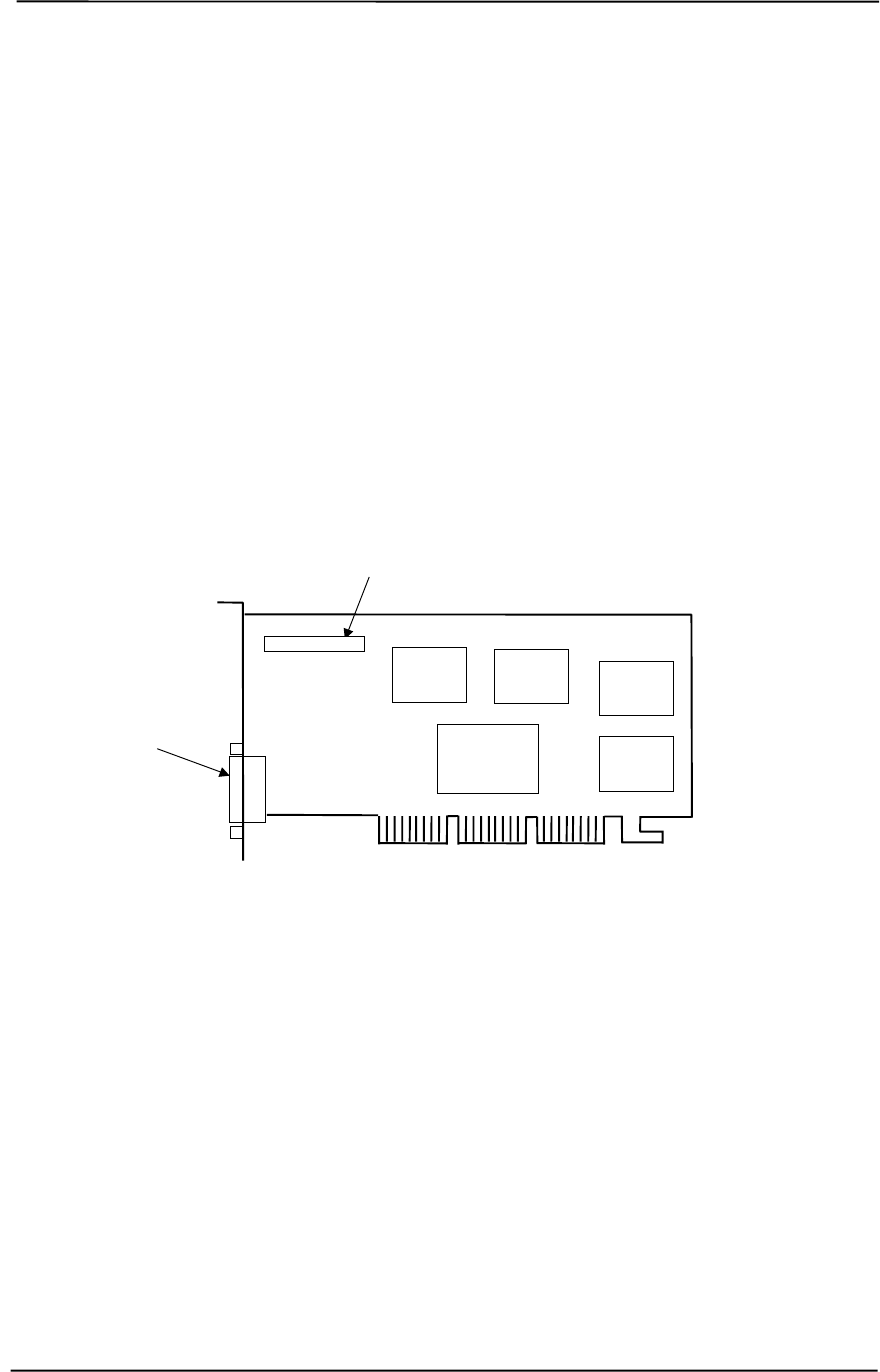
Technical Reference Guide
Compaq Personal Computers
Original - December 2000 J-1
Appendix J
COMPAQ/NVIDIA QUADRO2 MXR
AGP GRAPHICS CARD
J. Appendix J Compaq/NVIDIA Quadro2 MXR AGP Graphics
Card
J.1 INTRODUCTION
This appendix describes the Compaq/NVIDIA Quadro2 MXR AGP Graphics Card used in the
standard configuration on some models and also available as an option. This card (layout shown in
the following figure) installs in a system’s AGP slot. The Compaq/NVIDIA Quadro2 MXR
graphics card (SP# 221412-001) provides high 2D performance as well as entry-level 3D
capabilities.
Figure J-1. Compaq/NVIDIA Quadro2 MXR AGP Graphics Card (PCA# 221411-001) Layout
This appendix covers the following subjects:
♦ Functional description (D.2) page D-2
♦ Display modes (D.3) page D-3
♦ Software support information (D.4) page D-4
♦ Monitor power management (D.5) page D-4
♦ Connectors (D.6) page D-5
Feature Connector
NVIDIA
NV11GL
Controller SDRAM
SDRAM
SDRAM SDRAM
Analog
Monitor
Connector
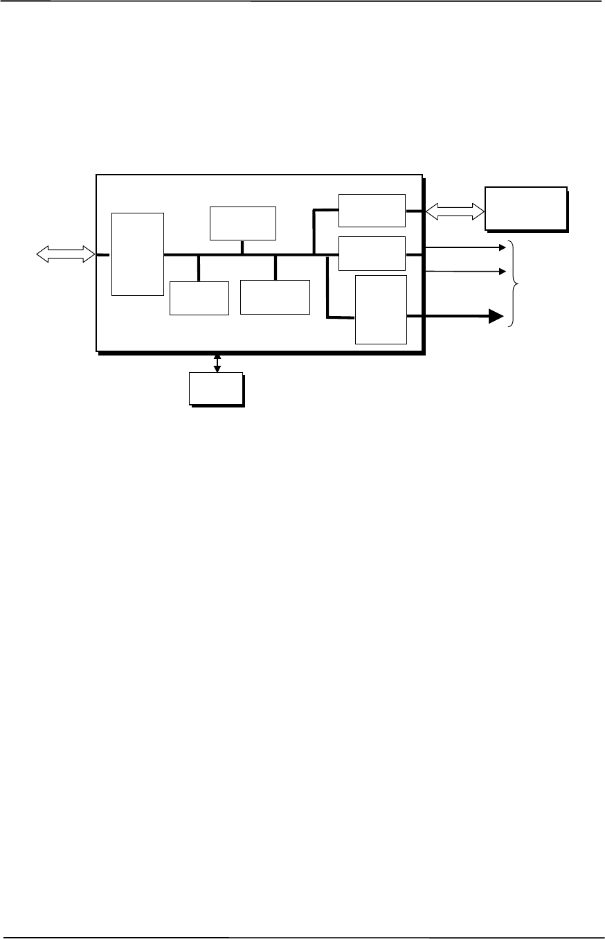
Appendix J Compaq/NVIDIA Quadro2 MXR AGP Graphics Card
Compaq Personal Computers
Original - December 2000
J-2
J.2 FUNCTIONAL DESCRIPTION
The NVIDIA Quadro2 MXR Graphics Card provides high performance 2D and 3D display
imaging. The card’s AGP design provides an economical approach to 3D processing by off-
loading 3D effects such as texturing, z-buffering and alpha blending to the system memory while
32 megabytes of on-board SDRAM stores the main display image.
Figure J-2. NVIDIA Quadro2 MXR Graphics Card Block diagram
The NVIDIA Quadro2 MXR Graphics Card includes the following features:
♦ 32-MB SDRAM frame buffer using 128-bit 183-MHz access
♦ AGP 4X transfers with sideband addressing
♦ 2D drawing engine
♦ 3D rendering engine
♦ 350-MHz RAMDAC
♦ 32-bit Z/stencil buffer eliminates hidden screen portions for faster loading
♦ 32-bit color for increased image quality
♦ 30-fps full-screen DVD playback
♦ Dual-monitor support with a PCI graphics card
BIOS
ROM
HSync
128-bit
166-MHz
Data Bus
Analog
Monitor
Connector
RGB
NVIDIA NV11GL Graphics Controller
3D Array
Engine
Video
Scalar
350-MHz
RAM
DAC
CRT
Controller
Memory
I/F
AGP
Bus
Card
Edge
Connector VSync
2D/VGA
Engine
32 MB
SDRAM
Frame Buffer
AGP 4X
I/F

Technical Reference Guide
Compaq Personal Computers
Original - December 2000 J-3
J.3 DISPLAY MODES
The 2D graphics display modes supported by the NVIDIA Quadro2 MXR Graphics are listed in
Table J-1.
Table J-1. NVIDIA Quadro2 MXR Graphics Display Modes
Table J-1.
NVIDIA Quadro2 MXR Graphics Display Modes
Resolution Bits per pixel Color Depth Max. Refresh
Frequency (Hz) [1] Memory Used
For Texture
640 x 480 8 256 240 N/A
640 x 480 16 65K 240 N/A
640 x 480 32 16.7M 240 28.4 MB
800 x 600 8 256 240 N/A
800 x 600 16 65K 240 N/A
800 x 600 32 16.7M 240 26.4 MB
1024 x 768 8 256 200 N/A
1024 x 768 16 65K 200 N/A
1024 x 768 32 16.7M 200 22.8 MB
1152 x 864 8 256 170 N/A
1152 x 864 16 65K 170 N/A
1152 x 864 32 16.7M 170 20.3 MB
1280 x 1024 8 256 150 N/A
1280 x 1024 16 65K 150 N/A
1280 x 1024 32 16.7M 150 16.6 MB
1600 x 1000 8 256 120 N/A
1600 x 1000 16 65K 120 22.6 MB
1600 x 1000 32 16.7M 120 13.3 MB
1600 x 1200 8 256 100 N/A
1600 x 1200 16 65K 100 20.8 MB
1600 x 1200 32 16.7M 100 9.5 MB
1600 x 1280 8 256 100 N/A
1600 x 1280 16 65K 100 20.0 MB
1600 x 1280 32 16.7M 100 8.0 MB
1920 x 1080 8 256 85 N/A
1920 x 1080 16 65K 85 19.9 MB
1920 x 1080 32 16.7M 85 7.7 MB
1920 x 1200 8 256 85 N/A
1920 x 1200 16 65K 85 18.5 MB
1920 x 1200 32 16.7M 85 5.0 MB
NOTE: [1] Values reflect hardware capability. May be restricted to lower frequency by operating system.

Appendix J Compaq/NVIDIA Quadro2 MXR AGP Graphics Card
Compaq Personal Computers
Original - December 2000
J-4
J.4 SOFTWARE SUPPORT INFORMATION
The NVIDIA Quadro2 MXR graphics card is fully compatible with software written for legacy
video modes (VGA, EGA, CGA) and needs no driver support for those modes.
Drivers are provided with or available for the card to provide extended mode support for the
current operating systems and programming environments such as:
♦ Windows 3.1, 95, 98, 2000, ME
♦ Windows NT 4.0, 3.51
♦ Whistler
♦ Linux
♦ OS/2
♦ Quick Draw
♦ MS Direct Draw and Direct X
♦ Direct 3D
♦ OpenGL
J.5 POWER MANAGEMENT AND CONSUMPTION
This controller provides monitor power control for monitors that conform to the VESA display
power management signaling (DPMS) protocol. This protocol defines different power
consumption conditions and uses the HSYNC and VSYNC signals to select a monitor’s power
condition. Table J-2 lists the monitor power conditions.
Table J-2. Monitor Power Management Conditions
Table J-2.
Monitor Power Management Conditions
HSYNC VSYNC Power Mode Description
Active Active On Monitor is completely powered up. If activated, the inactivity
counter counts down during system inactivity and if allowed to
timeout, generates an SMI to initiate the Suspend mode.
Active Inactive Suspend Monitor’s high voltage section is turned off and CRT heater
(filament) voltage is reduced from 6.6 to 4.4 VDC. The Off mode
inactivity timer counts down from the preset value and if allowed
to timeout, another SMI is generated and serviced, resulting in
the monitor being placed into the Off mode. Wake up from
Suspend mode is typically a few seconds.
Inactive Inactive Off Monitor’s high voltage section and heater circuitry is turned off.
Wake up from Off mode is a little longer than from Suspend.
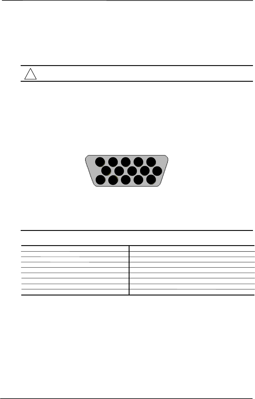
Technical Reference Guide
Compaq Personal Computers
Original - December 2000 J-5
J.6 CONNECTORS
There are two connectors associated with the graphics subsystem; the display/monitor connector
and the Feature connector.
NOTE: The graphic card’s edge connector mates with the AGP slot connector on the
system board. This interface is described in chapter 4 of this guide.
The DB-15 disply/monitor connector is provided for connection of a compatible RGB/analog
monitor. The Feature connector allows the attachment of an optional card such as a video tuner.
J.6.1 MONITOR CONNECTOR
Figure J-3. VGA Monitor Connector, (Female DB-15, as viewed from rear).
Table J-3. DB-15 Monitor Connector Pinout
Table F-3.
DB-15 Monitor Connector Pinout
Pin Signal Description Pin Signal Description
1 R Red Analog 9 PWR +5 VDC (fused) [1]
2 G Blue Analog 10 GND Ground
3 B Green Analog 11 NC Not Connected
4 NC Not Connected 12 SDA DDC2-B Data
5 GND Ground 13 HSync Horizontal Sync
6 R GND Red Analog Ground 14 VSync Vertical Sync
7 G GND Green Analog Ground 15 SCL DDC2-B Clock
8 B GND Blue Analog Ground -- -- --
NOTES: [1] Fuse automatically resets when excessive load is removed.
15 14 13 12 11
10 9 8 7 6
5 4 3 2 1

Appendix J Compaq/NVIDIA Quadro2 MXR AGP Graphics Card
Compaq Personal Computers
Original - December 2000
J-6
This page is intentionally blank.
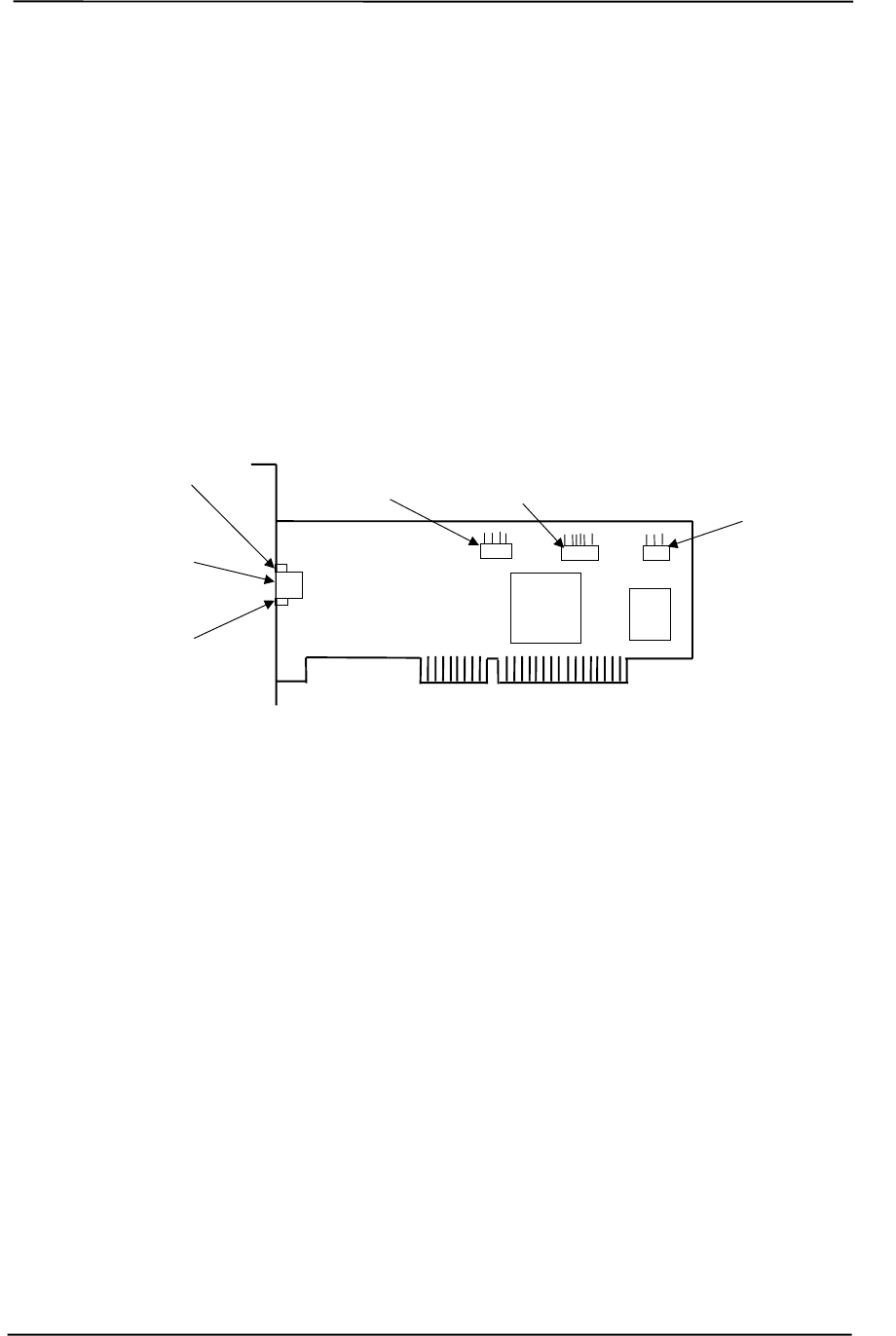
Technical Reference Guide
Compaq Personal Computers
Original - December 2000 K-1
Appendix K
COMPAQ PCI 10/100 ETHERNET ADAPTER
K. Appendix K Compaq PCI 10/100 Ethernet Adapter
K.1 INTRODUCTION
This appendix describes Compaq PCI 10/100 Ethernet Adapter (SP# 118042-001) that may be
included in the standard configuration on some models and available as options for all models.
The adapter card installs in a PCI slot to provide a system with network interface capability.
NOTE: Actual layout may vary.
Figure K-1. Compaq PCI 10/100 Ethernet Adapter Card Layout (PCA# 402355-001)
This appendix covers the following subjects:
♦ Functional description (K.2) page K-2
♦ Power management (K.3) page K-4
♦ Adapter programming (K.4) page K-5
♦ Network connector (K.5) page K-6
♦ Adapter specifications (K.6) page K-6
Link/Activity
LED
RJ-45
Network
Connector
Speed
LED
3C905C
NIC
WOL
Connector
AOL/SOS
Connector
SMBus
Connector
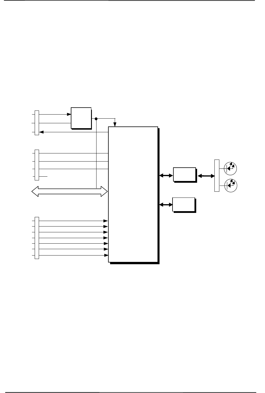
Appendix K Compaq PCI 10/100 Ethernet Adapter
Compaq Personal Computers
Original - December 2000
K-2
WOL
Conn.
TX/RX
WOL
GND
5 VDC Aux 3.3 VDC
1
2
3
4
SMB Data
SMB CS-
SMBus
Conn.
SMB Clock
NC
1 Event 1
AOL/SOS
Conn.
2
3
4
5
6
7
Event 2
Event 3
Event 4
Event 5
Event 6
MD Clock (SOS Present)
K.2 FUNCTIONAL DESCRIPTION
The Compaq PCI 10/100 NIC Adapter is based on the 3C905C Network Interface Controller
supported by firmware in flash ROM (Figure K-2). The adapter can operate in half- or full-duplex
modes and provide auto-negotiation of both mode and speed. Full-duplex operation follows the
IEEE 802.3x flow control specification. Transmit and receive FIFOs of three kilobytes each reduce
the chance of overrun while waiting for bus access. Each card includes an on-board 5/3.3 VDC
regulator circuit and WOL connector in support of Wake-On-LAN functionality.
Figure K-2. Compaq PCI 10/100 Ethernet Adapter, Block diagram
Key features of these adapters include:
♦ 2-KB transmit and 2-KB receive FIFOs
♦ 32-bit DMA bus mastering
♦ PCI ver. 2.2 compliant (PME- support)
♦ 10/100BASE-T half/full duplex (IEEE 802.3)
♦ Supports both 100BASE-TX and 100BASE-T4
♦ Nway 10/100 auto-negotiation support
♦ Both APM and ACPI power management support
♦ AOL/SOS interface for Remote Sense Alert support
♦ D0-D3 power state wake event support
♦ Boot ROM with PXE and RPL support
32-Bit
PCI Bus
PCI
Connector
5/3.3
VDC
Reg.
BIOS
ROM
Speed
RJ-45
Conn.
TX/RX
Mag.
Link/
Activit
y
1
2
3
3C905C
Ethernet Controller

Technical Reference Guide
Compaq Personal Computers
Original - December 2000 K-3
K.2.1 AOL FUNCTION
The adapter’s Alert-On-LAN (AOL) function provides a AOL-compliant system unit with the
ability to communicate system status to a management console, even while the system is powered
down. When installed in an AOL-compliant system, the adapter receives alert messages from the
system’s I/O Controller Hub (ICH) over the SMBus. Each alert message decoded by the adapter
results in a pre-constructed status message being transmitted over the network to a management
console. Alert-On-LAN functionality occurs independent of software, driver, or even processor
intervention. The adapter can report following conditions:
♦ System tampering – Removal of the chassis cover
♦ BIOS failure – System fails to boot successfully
♦ OS problem – System fails to load operating system after boot
♦ Missing/faulty processor – Processor fails to fetch first instruction
♦ Thermal condition – High temperature detected in system
♦ Heartbeat – Indication of system’s presence on the network (sent approximately every 30
seconds)
NOTE: The system unit must be plugged into a live AC outlet for the AOL function to be
operative. Controlling a system unit’s power through an AC outlet strip will, when
the strip is turned off, disable AOL functionality.
NOTE: Since AOL implements the SMBus, a cable connection from the SMBus
connector on the card to a corresponding SMBus connector on the system board may be
required. Compaq desktop system boards with AOL support inter-connect the SMBus
with the PCI bus and do not require a SMBus cable connection.
The AOL implementation requirements are as follows:
1. System unit featuring the 810, 810e, 820, or 850 (or later) chipset.
2. Intel PRO/100+ Management Adapter Driver 3.1 or later (available from Compaq).
3. Client-side utility agent software (available from Compaq).
4. Management console running one of the following:
a. HP OpenView Network Node Manager 6.x.
b. Intel LANDesk Client Manager.
c. Compaq Insight Manager.

Appendix K Compaq PCI 10/100 Ethernet Adapter
Compaq Personal Computers
Original - December 2000
K-4
K.2.2 RSA FUNCTION
This adapter provides support for systems using the Remote System Alert (RSA) method of
generating alerts over the network. The RSA method is similar to the AOL function described
previously but does not use the PCI’s SMBus for alert transactions. The RSA method uses an
AOL/SOS connector is provided on the card for connection to a compliant system board through a
7-conductor cable assembly. Up to six events may be detected by the adapter such as:
♦ BIOS fail
♦ OS fail
♦ Intrusion
♦ Fan alert
♦ Power alert
♦ Heartbeat
The RSA implementation requirements are as follows:
1. System unit featuring the 810, 810e, 820, or 850 (or later) chipset.
2. 7-conductor AOL/SOS cable assembly.
3. 3Com EtherDisk Driver 5.x or later (available from Compaq).
4. Client-side utility software (included with driver).
5. Server-side utility software (available from Compaq).
6. Management console running one of the following:
a. HP OpenView Network Node Manager 6.x.
b. Intel LANDesk Client Manager.
K.2.3 WAKE UP FUNCTIONS
The adapter provides two types of wake-up signaling: the PME- signal and the WOL signal.
The adapter provides PME- signal support for systems compliant with PCI ver. 2.2. The detection
of any wake event results in the adapter’s assertion of the PME- signal, which can be used by the
system unit to initiate the power-up sequence. System software is responsible for the clearing the
PME- signal.
The adapter also includes a WOL interface for systems supporting that method of wake-up. The
adapter asserts the WOL signal for 50 milliseconds upon detection of a Magic Packet. The WOL
signal is routed to the system unit (through a three-conductor cable connection) for initializing a
power-up sequence.

Technical Reference Guide
Compaq Personal Computers
Original - December 2000 K-5
K.3 POWER MANAGEMENT SUPPORT
These adapters support APM and ACPI power management environments as well as the Wired-
for-Management (WfM) and Wake-On-LAN (WOL) standards. The adapter is designed to be
powered up as long as the system unit is plugged into a live AC outlet to provide system “wake-
up” functionality. Power is provided by either the auxiliary 3.3 VDC power rail of the PCI bus
(when installed in systems compliant with PCI ver. 2.2) or by auxiliary 5 VDC through the WOL
connector.
NOTE: Controlling a system unit’s power through an AC outlet strip will, with the strip
turned off, disable wake-up functionality.
K.3.1 APM ENVIRONMENT
The Advanced Power Management (APM) functionality of system wake up is implemented
through the system’s APM-compliant BIOS and Magic Packet-compliant hardware. This
environment is not dependent on operating system (OS) intervention allowing a unit plugged into a
live AC outlet to be turned on remotely over the network (i.e., “remote wake-up”) even if the OS
has not been installed. In APM mode the controller will respond upon receiving a Magic Packet,
which is a packet where the node’s address is repeated 16 times. Upon Magic Packet reception, the
adapter asserts the PME- signal (on the PCI bus) resulting in the system unit’s power control logic
turning on the system and initiating the boot sequence. After the boot sequence the BIOS clears
the PME- signal so that subsequent wake up events will be detected.
K.3.2 ACPI ENVIRONMENT
The Advanced Configuration and Power Interface (ACPI) functionality of system wake up is
implemented through an ACPI-compliant OS (such as Windows NT 5.0) and is the default power
management mode. The following wake up events may be individually enabled/disabled through
the software driver supplied with the adapter:
♦ Magic Packet – Packet with node address repeated 16 times in data portion.
♦ Individual address match – Directed acket with matching user-defined byte mask.
♦ Multicast address match – Directed packet with matching user-defined sample frame.
♦ ARP (address resolution protocol) packet
♦ Flexible packet filtering – Packets that match defined CRC signature.
♦ NBT query (under IP 4.0)
♦ IPX Diagnostic
♦ TCO packet
♦ VLAN Type
When an enabled event is received the controller asserts the PME- signal that is used to initiate the
wakeup sequence.
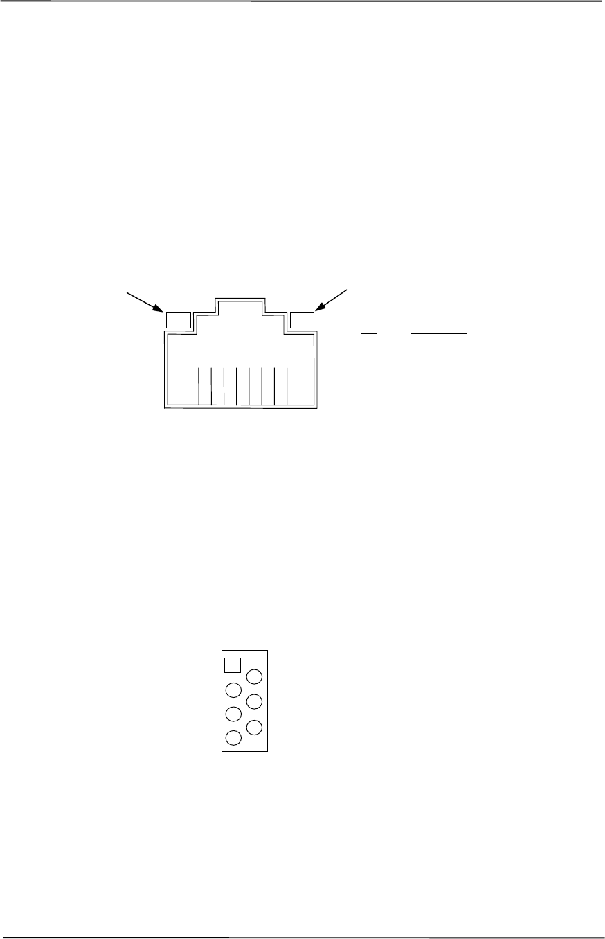
Appendix K Compaq PCI 10/100 Ethernet Adapter
Compaq Personal Computers
Original - December 2000
K-6
K.4 CONNECTORS
In addition to the PCI card edge connector, the NIC adapter includes four on-board connectors; the
RJ-45 network connector, an AOL/SOS connector, a WOL connector, and a SMBus connector.
K.4.1 NETWORK CONNECTOR
Figure K-3 shows the RJ-45 connector used for the NIC interface. This connector includes the two
status LEDs as part of the connector assembly.
Figure K-3. Ethernet TPE Connector (RJ-45, viewed from card edge)
K.4.2 AOL/SOS CONNECTOR
Figure K-4 shows the AOL/SOS connector. This connector is used for systems employing the
Remote System Alert (RSA) method of providing alerts to a network.
Figure K-4. AOL/SOS Connector (7-pin Header)
12438765
Pin Description
1 Transmit+
2 Transmit-
3 Receive+
6 Receive-
Activity LED
Speed LED
Pin Description
1 SOS1
2 SOS2
3 SOS3
4 SOS4
5 SOS5
6 SOS6
7 MDCLK (SOS present)
12
34
56
7

Technical Reference Guide
Compaq Personal Computers
Original - December 2000 K-7
K.4.3 SMBUS CONNECTOR
Figure K-5 shows the SMBus connector. This connector is used for systems employing AOL
functionality and requiring a cable connection for SMBus activity.
NOTE: Compaq desktop units do not require a cable connection for SMBus
activity.
Figure K-5. AOL/SOS Connector (4-pin Header)
K.4.4 WOL CONNECTOR
Figure K-6 shows the WOL connector. This connector is used for systems employing remote
wake-up.
Figure K-6. WOL Connector (3-pin Header)
Pin Description
1SMBus Data
2 SMBus CS-
3 SMBus Clock
4 Not connected
1
2
3
4
Pin Description
1 +5 VDC aux
2 Ground
3 Wake
1
2
3

Appendix K Compaq PCI 10/100 Ethernet Adapter
Compaq Personal Computers
Original - December 2000
K-8
K.5 ADAPTER SPECIFICATIONS
Table K-1. Adapter Specifications
Table K-1.
Adapter Specifications
Parameter
Modes Supported 10BASE-T half duplex @ 10 MB/s
10Base-T full duplex @ 20 MB/s
100BASE-TX half duplex @ 100 MB/s
100Base-TX full duplex @ 200 MB/s
Encryption Standards (82550 only) DES/3DES, HMAC SHA-1, MD5
Standards Compliance IEEE 802.1A, 802.1P, 802.1Q
IEEE 802.3, 802.3u, & 802.3x
Microsoft PC97, PC98, PC99
NetPC
DMI 1.0 & 2.0
WfM 1.1a & 2.0
OS Driver Support MS Windows 95 & 98
MS Windows NT 3.51 & 4.0
Boot ROM Support Intel PRO/100 Boot Agent (PXE 2.0, RPL)
F12 BIOS Support Yes
Bus Inteface PCI 2.2
Card size PCI half-length card
Power Management Support APM, ACPI, PCI Power Management Spec.
Power Comsumption 5.0 or 3.3 VDC @ 375 ma
Technical Reference Guide
Compaq Personal Computers
Original - December 2000 L-1
Appendix L
COMPAQ/ADAPTEC 29160N SCSI HOST ADAPTER
L. Appendix L Compaq/Adaptec SCSI Host Adapter
L.1 INTRODUCTION
The Compaq/Adaptec 29160N SCSI Host Adapter (Compaq SP# 158364-001) is a PCI peripheral
that provides high performance interfacing with compatible SCSI peripherals, typically SCSI hard
drives. The card installs in a PCI slot and supports full bus mastering capability.
This appendix covers the following subjects:
♦ Functional description (L.2) page L-2
♦ SCSI adapter programming (L.3) page L-3
♦ Specifications (L.4) page L-3
♦ SCSI connectors (L.5) page L-4
Figure L–1. Compaq/Adaptec 29160N SCSI Host Adapter Card Layout (PCA# 157342-001)
External
Ultra
SCSI Connector
Internal
Ultra SCSI Connector
Internal
Wide-Ultra SCSI Connector
AIC7892
Appendix K Compaq PCI 10/100 Ethernet Adapter
Compaq Personal Computers
Original - December 2000
L-2
L.2 FUNCTIONAL DESCRIPTION
A block diagram of the SCSI Adapter is shown in Figure L-2. The adapter’s architecture is based
on the AIC-7892 SCSI controller working off the 32-bit, 66-/33-MHz PCI bus. Providing full bus
mastering capability, the adapter supports data transfers up to 266 MB/s using the burst mode rate
on a 66-MHz 32-bit PCI bus. The AIC-7892 controller is an Ultra160 controller with an on-board
20-MIPS SCSI sequencer that can process SCSI commands without intervention from the host
microprocessor. The sequencer uses micro-code that is downloaded from the host during
initialization. Single-ended SCSI drivers are built into the controller and a 1-K data FIFO and an
internal 4-KB SRAM memory. An LED is provided to indicate SCSI bus activity.
The AIC7892 provides a memory interface that is used by the Serial EEPROM and the BIOS
ROM. The serial EEPROM stores non-volatile configuration data and the BIOS ROM (which is a
flash ROM) contains additional configuration data and SCSI functions. The programmable array
logic (PAL) controls the Serial EEPROM-to-AIC7892 interface.
Figure L–2. Compaq/Adaptec Ultra SCSI Adapter Card Block Diagram
The AIC7892 controller supports dual-mode low-voltage differential (LVD) SCSI I/O up to the
Ultra160 data rate of 160 Mbytes. Both single-ended (SE) and LVD devices can co-exist on the
SCSI bus, although operation will default to the SE mode. In SE mode, transfer rates are limited to
the speed of the slower device. High-voltage differential (HVD) devices are supported for rates up
to Ultra speeds.
The AIC7892 also supports cyclic redundancy check (CRC) codes, an improvement over parity
checking used earlier.
SCSI
Activity
PCI Bus AIC7892
SCSI
Controller
Serial
EEPROM
BIOS
ROM
40-MHz
Clock
Int. SCSI Connector (SE)
Ext. SCSI Connector (SE)
AIC3860
Transceiver
Chip
PCI
Slot
Int. SCSI Connector (SE/LVD)
Active Ultra160
SE/LVD Term.
Active Ultra160
SE Term.
PAL
Chip

Technical Reference Guide
Compaq Personal Computers
Original - December 2000 L-3
L.3 SCSI ADAPTER PROGRAMMING
L.3.1 SCSI ADAPTER CONFIGURATION
The Adaptec SCSI Host Adapter Card is a PCI device and configured using PCI protocol and PCI
Configuration Space registers (PCI addresses 00h-FFh) as discussed in Chapter 4 of this guide.
Configuration is accomplished by BIOS during POST and re-configurable with software. The
vender ID and device ID for the adapter are as follows:
Vender ID (PCI config. addr. 00h): 9005h
Device ID (PCI config, addr. 02h): 0080h
L.3.2 SCSI ADAPTER CONTROL
Control of the SCSI host adapter is affected through I/O mapped registers mapped as listed in
Table L-1.
Table L–1. SCSI Host Adapter Card Control Register Mapping
Table L-1.
Ultra SCSI Host Adapter Card
Control Register Mapping
I/O Addr. Function
n00h-n1Fh SCSI Register Array
n20h-n5Fh Scratch RAM
n60h-n7Fh Phase Engine (Sequencer)
n80h-n9Fh Host Registers
n00h-nFFh SCB Array
n = prefix address supplied by the BASEADR0 PCI Config. Reg.
L.4 SPECIFICATIONS
The operating specifications are listed in Table L-2.
Table L–2. Ultra SCSI Host Adapter Card Specifications
Table L-2.
Ultra SCSI Host Adapter Card Specifications
Operating Voltage +5 VDC
Maximum Current Draw 2 A
Operating Temperature 32°F (0°C) to 131°F (55°C)
Appendix K Compaq PCI 10/100 Ethernet Adapter
Compaq Personal Computers
Original - December 2000
L-4
L.5 SCSI CONNECTORS
This SCSI card provides two internal header-type connectors (one 50-pin, one 68-pin) and one
external D-type connector (50-pin).
L.5.1 EXTERNAL 50-PIN ULTRA SCSI CONNECTOR
The card provides one external 50-pin D-type Ultra SCSI connector. External cabling should meet
T-10 SPI-2 standards (50-conductor, round shielded).
Figure L–3. External Ultra SCSI Connector (50-pin)
Table L–3. External 50-Pin Ultra SCSI Connector Pinout
Table L-3.
External Ultra SCSI Connector Pinout
Pin Signal Function Pin Signal Function
1 GND Ground 26 DB0- Data Bit 0
2 GND Ground 27 DB1- Data Bit 1
3 GND Ground 28 DB2- Data Bit 2
4 GND Ground 29 DB3- Data Bit 3
5 GND Ground 30 DB4- Data Bit 4
6 GND Ground 31 DB5- Data Bit 5
7 GND Ground 32 DB6- Data Bit 6
8 GND Ground 33 DB7- Data Bit 7
9 GND Ground 34 DBP Data Bus Pulse
10 GND Ground 35 GND Ground
11 GND Ground 36 GND Ground
12 GND Ground 37 GND Ground
13 RSVD Reserved 38 TERMPWR Termination Power
14 GND Ground 39 GND Ground
15 GND Ground 40 GND Ground
16 GND Ground 41 ATN- Attention
17 GND Ground 42 GND Ground
18 GND Ground 43 BSY- Busy
19 GND Ground 44 ACK- Acknowledge
20 GND Ground 45 SBRST- Burst
21 GND Ground 46 MSG- Message Activity
22 GND Ground 47 SEL- Select
23 GND Ground 48 C-/D Control/Data Transfer Indicator
24 GND Ground 49 REQ- Request
25 GND Ground 50 I-/O Input/Output Indicator
Pin 1

Technical Reference Guide
Compaq Personal Computers
Original - December 2000 L-5
L.5.2 INTERNAL 50-PIN ULTRA SCSI CONNECTOR
The card provides one internal 50-pin header-type Ultra SCSI connector. Internal cabling to this
connector should consists of an unshielded connector with a 50-conductor flat cable as specified in
ANSI standard X3T9.2/375R.
Figure L–4. Internal 50-Pin Ultra SCSI Connector
Table L–4. Internal 50-Pin Ultra SCSI Connector Pinout
Table L-4.
Internal 50-Pin Ultra SCSI Connector Pinout
Pin Signal Function Pin Signal Function
1 GND Ground 2 DB0- Data Bit 0
3 GND Ground 4 DB1- Data Bit 1
5 GND Ground 6 DB2- Data Bit 2
7 GND Ground 8 DB3- Data Bit 3
9 GND Ground 10 DB4- Data Bit 4
11 GND Ground 12 DB5- Data Bit 5
13 GND Ground 14 DB6- Data Bit 6
15 GND Ground 16 DB7- Data Bit 7
17 GND Ground 18 DBP Data Bus Pulse
19 GND Ground 20 GND Ground
21 GND Ground 22 CS Cable Sense
23 Open Open 24 Open Open
25 Open Open 26 TERMPWR Termination Power
27 Open Open 28 Open Open
29 GND Ground 30 GND Ground
31 GND Ground 32 ATN- Attention
33 GND Ground 34 GND Ground
35 GND Ground 36 BSY- Busy
37 GND Ground 38 ACK- Acknowledge
39 GND Ground 40 SBRST- Reset
41 GND Ground 42 MSG- Message Activity
43 GND Ground 44 SEL- Select
45 GND Ground 46 C-/D Control/Data Transfer Indicator
47 GND Ground 48 REQ- Request
49 GND Ground 50 I-/O Input/Output Indicator
Pin 1
Pin 2
Pin 50
Pin 49

Appendix K Compaq PCI 10/100 Ethernet Adapter
Compaq Personal Computers
Original - December 2000
L-6
L.5.3 INTERNAL 68-PIN ULTRA160 SCSI CONNECTOR
The card provides one internal 68-pin Ultra160 SCSI connector. This connection is designed for a
68-conductor unshielded Twist ‘N Flat cable as specified in the T-10 SPI-2 standard.
Figure L–5. Ultra 160 SCSI Connector (68-pin header type)
Table L–5. Ultra160 SCSI Connector Pinout
Table L-5.
Ultra160 SCSI Connector Pinout
Pin Signal Function Pin Signal Function
1 GND Ground 35 DB12 Data Bit 12
2 GND Ground 36 DB13 Data Bit 13
3 GND Ground 37 DB14 Data Bit 14
4 GND Ground 38 DB15 Data Bit 15
5 GND Ground 39 DBP- Data Bus Parity
6 GND Ground 40 DB0- Data Bit 0
7 GND Ground 41 DB1- Data Bit 1
8 GND Ground 42 DB2- Data Bit 2
9 GND Ground 43 DB3- Data Bit 3
10 GND Ground 44 DB4- Data Bit 4
11 GND Ground 45 DB5- Data Bit 5
12 GND Ground 46 DB6- Data Bit 6
13 GND Ground 47 DB7- Data Bit 7
14 GND Ground 48 DBP- Data Bus Parity
15 GND Ground 49 GND Ground
16 GND Ground 50 GND Ground
17 TERMPWR Termination Power 51 TERMPWR Termination Power
18 TERMPWR Termination Power 52 TERMPWR Termination Power
19 GND Ground 53 Int_Out- Interrupt Out
20 GND Ground 54 SBRST- Burst
21 GND Ground 55 ATN- Attention
22 GND Ground 56 GND Ground
23 GND Ground 57 BSY- Busy
24 GND Ground 58 ACK- Acknowledge
25 GND Ground 59 RESET- Reset
26 GND Ground 60 MSG- Message Activity
27 GND Ground 61 SEL- Select
28 GND Ground 62 C-/D Control/Data Transfer Indicator
29 GND Ground 63 REQ- Request
30 GND Ground 64 I-/O Input/Output Indicator
31 GND Ground 65 DB8- Data Bit 8
32 GND Ground 66 DB9- Data Bit 9
33 GND Ground 67 DB10- Data Bit 10
34 GND Ground 68 DB11- Data Bit 11
Pin 1
Pin 35
Pin 34
Pin 68

INDEX
I.
3D effects, D-2, E-2, G-2, H-2, J-2
abbreviations, 1-3
AC97 link bus, 5-29
Accelerated Graphics Port (AGP), 4-10
ACPI, I-5, K-5
acronyms, 1-3
AGP, 4-10
Alert-On-LAN, 5-33
AOL, 5-33
AOL requirements, 5-34, 5-36
APIC, 4-16
APM, I-5, K-5
APM BIOS support, 7-19
arbitration, PCI bus master, 4-6
ASCII character set, B-1
audio, 5-26
audio controller (AC97), 5-28
audio subsystem, 2-14
backplane, 2-6
battery replacement, 4-20
BIOS, ROM, 7-1
blinking LED, 6-4
boot block ROM, 7-2
boot status, 4-33
cable lock, 4-32
Celeron processor, 2-10
chipsets, 2-11
Client Management, 7-12
clock generation, 4-20
CMOS, 4-20
CMOS, archive, 4-22
CMOS, clearing, 4-21
CMOS, restoring, 4-22
codec, audio, 5-30
Configuration Cycle, 4-4
configuration cycle (PCI), 4-4
configuration memory, 4-20
configuration space (PCI), 4-5
connector
RJ-11 (modem), F-4
Connector
AGP bus, 4-14
Audio, CD, 5-27
audio, headphones out, 5-26
audio, line in, 5-26
audio, line out, 5-26
Audio, Mic In, 5-26
Audio, Speaker, 5-27
diskette drive interface, 5-7
display (VGA monitor), D-5, E-5, G-5, H-5, J-
5
IDE interface, 5-3
keyboard/pointing device interface, 5-21
Network RJ-45, 5-36
parallel interface, 5-15
PCI bus, 4-9
serial interface (RS-232), 5-8
Ultra SCSI (50-pin D-type), L-4
Ultra SCSI (50-pin header type), L-5
Universal Serial Bus interface, 5-25
VGA pass-through (feature), E-6, G-6, H-6
Wide Ultra SCSI (68-pin header type), L-6
continuity module, 3-6
cooling, 4-34
core voltage, 6-6
CRIMM, 3-6
Data Encryption Standards (DES), I-4
DES, I-4
device ID (PCI), 4-4
DIMM detection, 7-5
DIMM support, 7-14
Direct Rambus, 3-5
diskette drive interface, 5-4
display modes, D-3, E-3, G-3, H-3, J-3
DMA, 4-19
DMI, 7-16
drive fault prediction, 7-15
DSP, F-2
dual-head support, H-2
East Access keys, C-10
Easy Access keyboards, C-7
effects, 3D, D-2, E-2, G-2, H-2, J-2
EIDE interface, 5-1
Enhanced Parallel Port (EPP), 5-12
events, wake up, 6-4
expansion card cage, 2-6
Extended Capabilities Port (ECP), 5-12
features, standard, 2-2
flash ROM, 7-2
flash status, 4-33
general purpose I/O, 4-36
GPIO, 4-36
I/O controller, 4-38
graphics card, D-1, E-1, F-1, G-1, H-1, J-1, K-1,
L-1
graphics subsystem, 2-13
graphics, 3D, D-2, E-2, G-2, H-2, J-2
Hard drive activity indicator, 4-39
Hub link bus, 4-7
I/O controller (LPC47B34x), 4-37
I/O map, 4-35
IDE interface, 5-1
IDSEL, 4-4
index addressing, 1-2
interface
audio, 2-14, 5-26
diskette drive, 5-4
IDE, 5-1
keyboard/pointing device, 5-16
parallel, 2-12, 5-11
serial, 2-12, 5-8
USB, 2-12, 5-22
interrupts
maskable (IRQn), 4-15
nonmaskable (NMI, SMI), 4-17
interrupts, PCI, 4-7
IPSEC, I-4
K56Flex, F-2
key (keyboard) functions, C-8
keyboard, C-1
keyboard (micro)processor, C-2
keyboard layouts, C-5
keyboard, USB, C-4
keyboards, Easy Access, C-7
keys, Easy Access, C-10
keys, Windows, C-9
LED indications, 6-3, 6-4
LED indications (status), 4-33, 4-39
LED, HD, 4-39
LED, network status, K-2
LED, Power, 4-39
LEDs, system board, 6-3
Low Pin-Count (LPC) Bus, 4-7
low voltages, 6-6
LPC bus, 4-7
LPC47B34x I/O controller, 4-37
mass storage, 2-12
memory detection, 7-5
memory map, 3-9
memory, system (RAM), 2-12
microphone, 5-26
monitor power control, D-4, E-4, G-4, H-4, J-4
mouse interface, 5-18
network interface controller card, I-1
network support, 5-33
NIC card, I-1
NLX card, K-1
notational conventions, 1-1, 1-2
operational status indications (LED), 4-33
option ROM, 4-7
options, 2-3
packet (Rambus), 3-7
parallel interface, 2-12, 5-11
password, clearing, 4-21
password, power-on, 4-31
PC600/700/800, 3-6
PCI bus, 4-2
PCI Configuration Space, 4-5
PCI interrupts, 4-7
PCI modem, F-2
PCI ver. 2.2, 5-33
Pentium 4 processor, 3-2
Pentium II, 2-11
Pentium II processor, 2-10
pinouts, header (connector), 6-8
Plug ’n Play, 2-2, 2-12, 7-15
Plug 'n Play BIOS function, 7-15
power button, 6-3
Power Button Override, 4-22
power consumption, graphics card, D-4
power distribution, 6-5
Power indicator, 4-39
power LED, 6-4
power management
ACPI, 4-32
PCI, 4-7
Rambus, 3-8
power management BIOS function, 7-17
power mangement, F-4
power supply, 6-1
power supply assembly, 6-2
power-on password, 4-31
processor upgrading, 3-4
processor, Celeron, 2-10
processor, Pentium 4, 3-2
processor, Pentium II, 2-10
RAM, 2-12
Rambus, 3-5
RDRAM, 3-5
reference sources, 1-1
remote flashing, 7-2
remote sense alert, 5-35
restoring CMOS, 4-22
RIMM, 3-5, 3-6
ROM BIOS, 7-1
ROM flashing, 7-2
ROM, option, 4-7
RS-232, 5-8
RTC, 4-20
scan codes (keyboard), C-11
SDRAM, E-2, G-2, H-2
security functions, 4-31
security, interface, 4-32
sensor, thermal, 4-34
serial interface, 2-12, 5-8
SGRAM, D-2, J-2
sideband addressing, 4-11
signal distribution, 6-7, 6-8
SMBIOS, 7-16
SMI, 4-18
Sound Blaster 128 audio, 5-26
specifications
electrical, 2-14
environmental, 2-14
physical, 2-15
power supply, 6-7, 6-8
Specifications
8x CD-ROM Drive, 2-16
Audio subsystem, 5-32
Diskette Drive, 2-15
SCSI Host Adapter, L-3
specifications, network adapter, I-7, K-8
specifications, system, 2-14
SSE2, 3-2
status, system (LED), 4-33, 4-39
system board, 2-7
system board LEDs, 6-3
system ID, 7-6, 7-14
system memory, 2-12
system resources, 4-15
system ROM, 7-1
system status indications, 4-33, 4-39
TAFI, 4-34
temperature status, 7-14
thermal sensing, 4-34
transmission modes (modem), F-3
troubleshooting, 6-3
typematic, C-8
UART, 5-8, F-2
UART transfer modes (modem), F-3
Universal Serial Bus (USB) interface, 5-22
upgrading, BIOS, 7-2
upgrading, processor, 3-4
USB interface, 5-22
USB keyboard, C-4
USB legacy support, 7-23
USB ports, 2-12
V.90, F-2
vender ID (PCI), 4-4
VESA connector, E-6, G-6, H-6
voltage, core, 6-6
wake up (power), 6-4
wake up events, 6-4
Wake-On-LAN, 6-4
Windows keys, C-9
WOL, 6-4, I-5, K-5, K-7
This page is intentionally blank.
